EP1229552B1 - Einmalig programmierbare nichtflüchtige halbleiterspeicheranordnung und verfahren zu deren herstellung - Google Patents
Einmalig programmierbare nichtflüchtige halbleiterspeicheranordnung und verfahren zu deren herstellung Download PDFInfo
- Publication number
- EP1229552B1 EP1229552B1 EP20010401707 EP01401707A EP1229552B1 EP 1229552 B1 EP1229552 B1 EP 1229552B1 EP 20010401707 EP20010401707 EP 20010401707 EP 01401707 A EP01401707 A EP 01401707A EP 1229552 B1 EP1229552 B1 EP 1229552B1
- Authority
- EP
- European Patent Office
- Prior art keywords
- semiconductor
- insulating film
- semiconductor layer
- memory device
- nonvolatile memory
- Prior art date
- Legal status (The legal status is an assumption and is not a legal conclusion. Google has not performed a legal analysis and makes no representation as to the accuracy of the status listed.)
- Expired - Lifetime
Links
Images


Classifications
-
- H—ELECTRICITY
- H10—SEMICONDUCTOR DEVICES; ELECTRIC SOLID-STATE DEVICES NOT OTHERWISE PROVIDED FOR
- H10B—ELECTRONIC MEMORY DEVICES
- H10B69/00—Erasable-and-programmable ROM [EPROM] devices not provided for in groups H10B41/00 - H10B63/00, e.g. ultraviolet erasable-and-programmable ROM [UVEPROM] devices
-
- G—PHYSICS
- G11—INFORMATION STORAGE
- G11C—STATIC STORES
- G11C17/00—Read-only memories programmable only once; Semi-permanent stores, e.g. manually-replaceable information cards
- G11C17/14—Read-only memories programmable only once; Semi-permanent stores, e.g. manually-replaceable information cards in which contents are determined by selectively establishing, breaking or modifying connecting links by permanently altering the state of coupling elements, e.g. PROM
- G11C17/16—Read-only memories programmable only once; Semi-permanent stores, e.g. manually-replaceable information cards in which contents are determined by selectively establishing, breaking or modifying connecting links by permanently altering the state of coupling elements, e.g. PROM using electrically-fusible links
-
- H—ELECTRICITY
- H10—SEMICONDUCTOR DEVICES; ELECTRIC SOLID-STATE DEVICES NOT OTHERWISE PROVIDED FOR
- H10B—ELECTRONIC MEMORY DEVICES
- H10B20/00—Read-only memory [ROM] devices
-
- H—ELECTRICITY
- H10—SEMICONDUCTOR DEVICES; ELECTRIC SOLID-STATE DEVICES NOT OTHERWISE PROVIDED FOR
- H10B—ELECTRONIC MEMORY DEVICES
- H10B99/00—Subject matter not provided for in other groups of this subclass
-
- H—ELECTRICITY
- H10—SEMICONDUCTOR DEVICES; ELECTRIC SOLID-STATE DEVICES NOT OTHERWISE PROVIDED FOR
- H10D—INORGANIC ELECTRIC SEMICONDUCTOR DEVICES
- H10D30/00—Field-effect transistors [FET]
- H10D30/60—Insulated-gate field-effect transistors [IGFET]
- H10D30/68—Floating-gate IGFETs
-
- G—PHYSICS
- G11—INFORMATION STORAGE
- G11C—STATIC STORES
- G11C2213/00—Indexing scheme relating to G11C13/00 for features not covered by this group
- G11C2213/30—Resistive cell, memory material aspects
- G11C2213/33—Material including silicon
-
- G—PHYSICS
- G11—INFORMATION STORAGE
- G11C—STATIC STORES
- G11C2213/00—Indexing scheme relating to G11C13/00 for features not covered by this group
- G11C2213/70—Resistive array aspects
- G11C2213/71—Three dimensional array
-
- G—PHYSICS
- G11—INFORMATION STORAGE
- G11C—STATIC STORES
- G11C2213/00—Indexing scheme relating to G11C13/00 for features not covered by this group
- G11C2213/70—Resistive array aspects
- G11C2213/77—Array wherein the memory element being directly connected to the bit lines and word lines without any access device being used
-
- G—PHYSICS
- G11—INFORMATION STORAGE
- G11C—STATIC STORES
- G11C2213/00—Indexing scheme relating to G11C13/00 for features not covered by this group
- G11C2213/70—Resistive array aspects
- G11C2213/79—Array wherein the access device being a transistor
-
- H—ELECTRICITY
- H10—SEMICONDUCTOR DEVICES; ELECTRIC SOLID-STATE DEVICES NOT OTHERWISE PROVIDED FOR
- H10W—GENERIC PACKAGES, INTERCONNECTIONS, CONNECTORS OR OTHER CONSTRUCTIONAL DETAILS OF DEVICES COVERED BY CLASS H10
- H10W90/00—Package configurations
- H10W90/20—Configurations of stacked chips
- H10W90/28—Configurations of stacked chips the stacked chips having different sizes, e.g. chip stacks having a pyramidal shape
Definitions
- the present invention relates to a semiconductor nonvolatile memory device and a method for production of the same, more particularly relates to an OTP (one time programmable) semiconductor nonvolatile memory device capable of being written with data only one time and a method for production of the same.
- OTP one time programmable
- nonvolatile semiconductor memory devices floating gate type, MNOS type, MONOS type, and other flash memories having various characteristics and capable of erasing data together have been developed. They have CMOS transistors as decoders and other peripheral transistors of memory cell arrays.
- Japanese Examined Patent Publication (Kokoku) No. 4-9388 discloses a memory cell having a structure shown in Fig. 1.
- a gate electrode 104 is formed on a channel forming region 102 of a p-type semiconductor substrate 101 via a gate insulating film 103, and a source region 105 and a drain region 106 containing n-type impurities are formed in the semiconductor substrate 101 on the two sides thereof, whereby a MOS field-effect transistor is formed.
- An insulating film 110 of silicon oxide is formed covering the MOS transistor, contact holes reaching the gate electrode 104, source region 105, and the drain region 106 are formed, and a gate interconnection 115, source interconnection 116, and a drain interconnection 117 made of for example aluminum are filled in the contact holes.
- a silicon oxide film 114 is formed at an interface between the source region 105 and the drain interconnection 116 and insulates the two.
- a memory cell having the above structure by applying a high voltage between the source region 105 and the source interconnection 116 according to the data to be written, the insulation in the silicon oxide film 114 is broken and the source region 105 and the source interconnection 116 are made conductive.
- data can be stored by conduction or nonconduction between the source region 105 and the source interconnection 116 in each memory cell.
- Japanese Examined Patent Publication (Kokoku) No. 58-28750 and Japanese Examined Patent Publication (Kokoku) No. 63-22073 disclose memory cells having structures shown in Fig. 2 and Fig. 3 are disclosed.
- a polysilicon layer 120 is formed connected to the source region 105, and the source interconnection 116 is formed at an upper layer thereof via the silicon oxide film 114.
- the polysilicon layer 120 is formed also in the drain region 106, and the drain interconnection 117 is formed at an upper layer thereof.
- U.S. Patent No. 6,034,882 discloses a semiconductor nonvolatile memory device having a memory cell array and having a peripheral circuit shown in an equivalent circuit diagram of Fig. 4A.
- memory cells M are provided at intersecting points of conductive layers (C1, C3, C5, C7) receiving layer selection signals LSS by a switching transistor SWT controlled by a row decoder RD and conductive layers (C2, C4, C6) acting as the bit lines BL.
- the above memory cell has a structure shown in for example Fig. 4B.
- a p + type polysilicon layer 202 is formed on a conductive layer 201 forming the conductive layers (C1, C3, C5, C7), and an n-type polysilicon layer 203 is formed at an upper layer thereof to thereby form a diode.
- a silicon oxide film 204 is formed at an upper layer of the polysilicon layer 203, an n + type polysilicon layer 205 is formed at an upper layer thereof, and a conductive layer 206 forming the conductive layers (C2, C4, C6) is laid at an upper layer thereof.
- the polysilicon layer 203 and the polysilicon layer 205 are insulated by the silicon oxide film 204.
- a memory cell having the above structure by applying a high voltage between the polysilicon layer 203 and the polysilicon layer 205 according to the data to be written, the insulation in the silicon oxide film 204 is broken and the polysilicon layer 203 and the polysilicon layer 205 are made conductive. Therefore, data can be stored according to existence/nonexistence of the diode element in each memory cell (portion where the polysilicon layer 202 and the polysilicon layer 203 are stacked).
- the semiconductor nonvolatile memory device shown in Figs. 4A and 4B is configured by memory cells each comprised of a fuse of an insulating film breakage type and a diode as an active element connected therein repeating in three dimensions. Therefore, it becomes necessary to form a silicon layer having a crystallinity required for comprising the active element in an upper layer of the interconnection made of aluminum, so there is a large influence of heat treatment upon the aluminum interconnections and accompanying major difficulties in actual production.
- An object of the present invention is to provide a semiconductor nonvolatile memory device capable of improving the reproducibility and reliability of the breakage of insulation of the silicon oxide film and capable of further reducing the manufacturing cost and a method for production of the same.
- a semiconductor nonvolatile memory device of the present invention has at least one memory cell and is programmable one time, wherein the memory cell comprises an impurity region of a first conductivity type formed in a semiconductor substrate, a first insulating film formed on the semiconductor substrate covering the impurity region, an opening formed in the first insulating film so as to reach the impurity region, and a program portion comprising a first semiconductor layer of the first conductivity type, a second insulating film, and a second semiconductor layer of a second conductivity type, the first semiconductor layer, the second insulating film and the second semiconductor layer being successively stacked in the opening, the first semiconductor layer being formed on the impurity region, the second insulating film being changed in a conductive state in response to a program data to thereby electrically connect between the first and second semiconductor layers.
- insulation breakage in the second insulating film in the program portion is caused by applying a predetermined voltage between the first semiconductor layer and the second semiconductor layer in response to the program data to be stored in the memory cell, and data is stored by the conduction or nonconduction between the first semiconductor layer and the second semiconductor layer in each memory cell.
- a gate electrode acting as a word line is formed on the semiconductor substrate via a gate insulating film, a channel forming region is provided on the semiconductor substrate below the gate electrode, a field-effect transistor using the impurity region as the drain region is formed, and the bit line is connected to the second semiconductor layer.
- the source region of the field-effect transistor is grounded.
- the word line and the bit line are connected to a row decoder and a column decoder including pass transistors for passing supplied signals therethrough, and more preferably, inverted signals of address signals are supplied to the row decoder and the column decoder from an external device together with forward signals.
- the plurality of memory cells are arranged in a matrix form.
- the memory cell has an impurity region of a first conductivity type formed on the semiconductor substrate, a first insulating film formed on the semiconductor substrate while covering the impurity region, an opening formed in the first insulating film so as to reach the impurity region, and a first semiconductor layer of a first conductivity type, a second insulating film, and a second semiconductor layer of a second conductivity type successively stacked in the opening from the impurity region side.
- the reproducibility and reliability are improved, and insulation breakage in the second insulating film can be caused.
- a memory cell can be comprised by a simple structure, by making for example the row decoder and the column decoder by only pass transistors, the device can be produced while reducing the number of masks to about six, so the manufacturing cost can be suppressed.
- a semiconductor nonvolatile memory device of the present invention has at least one memory cell and is programmable one time, wherein the memory cell comprises a first interconnection, a first insulating film formed on the first interconnection, an opening formed in the first insulating film so as to reach the first interconnection, a program portion comprising a first semiconductor layer of a first conductivity type, a second insulating film, and a second semiconductor layer of a second conductivity type, the first semiconductor layer, the second insulating film and the second semiconductor layer being successively stacked in the opening, the first semiconductor layer being formed on the first interconnection, the second insulating film being changed in a conductive state in response to a program data to thereby electrically connect between the first and second semiconductor layers, and a second interconnection formed connected to the second semiconductor layer.
- insulation breakage in the second insulating film in the program portion is caused by applying a predetermined voltage between the first semiconductor layer and the second semiconductor layer in response to the program data to be stored in the memory cell, and data is stored by the conduction or nonconduction between the first semiconductor layer and the second semiconductor layer in each memory cell.
- the first interconnection is a word line and the second interconnection is a bit line.
- the word line and the bit line are connected to a row decoder and a column decoder including pass transistors for passing supplied signals therethrough.
- inverted signals of address signals are supplied to the row decoder and the column decoder from an external device together with the forward signals.
- the plurality of memory cells are arranged in a matrix form.
- a plurality of stacks of the first interconnection, first insulating film, and second interconnection are stacked while being insulated from each other, and in each stack, the plurality of memory cells are arranged in a matrix form so as to be connected to the first interconnection and the second interconnection.
- the memory cell has the first interconnection, first insulating film formed on the first interconnection, opening formed in the first insulating film so as to reach the first interconnection, first semiconductor layer of a first conductivity type, second insulating film, and second semiconductor layer of a second conductivity type successively stacked in the opening from the first interconnection side, and the second interconnection formed connected to the second semiconductor layer.
- the reproducibility and reliability are improved, and insulation breakage in the second insulating film can be caused.
- the memory cell can be comprised by a simple structure, by making for example the row decoder and the column decoder by only pass transistors, the device can be produced while reducing the number of masks to about six, so the manufacturing cost can be suppressed.
- a semiconductor nonvolatile memory device of the present invention has at least one memory cell and is programmable one time, wherein the memory cell comprises an impurity region of a first conductivity type formed in a first semiconductor layer on an insulating substrate, a first insulating film formed on the first semiconductor layer while covering the impurity region, an opening formed in the first insulating film so as to reach the impurity region, and a program portion comprising a second insulating film and a second semiconductor layer of a second conductivity type, the second insulating film and the second semiconductor layer being successively stacked in the opening, the second insulating film being formed on the impurity region, the second insulating film being changed in a conductive state in response to a program data to thereby electrically connect between the impurity region and the second semiconductor layer.
- the insulation breakage in the second insulating film in the program portion is caused by applying a predetermined voltage between the impurity region and the second semiconductor layer in response to the program data to be stored in the memory cell, and data is stored by the conduction or nonconduction between the impurity region and the second semiconductor layer in each memory cell.
- a gate electrode forming the word line is formed on the first semiconductor layer via a gate insulating film, a channel forming region is provided in the first semiconductor layer below the gate electrode, a field-effect transistor is formed using the impurity region as the drain region, and a bit line is connected to the second semiconductor layer.
- the source region of the field-effect transistor is grounded.
- the word line and the bit line are connected to a row decoder and a column decoder including pass transistors for passing supplied signals therethrough, and more preferably, inverted signals of address signals are supplied to the row decoder and the column decoder from an external device together with forward signals.
- the plurality of memory cells are arranged in the matrix form.
- the semiconductor nonvolatile memory device of the present invention preferably a plurality of the first semiconductor layers are stacked while being insulated from each other, and the memory cells are arranged in a matrix form in each of the first semiconductor layers.
- the memory cell has an impurity region of a first conductivity type formed in the first semiconductor layer on the insulating substrate, a first insulating film formed on the first semiconductor layer while covering the impurity region, an opening formed in the first insulating film so as to reach the impurity region, and a second insulating film and second semiconductor layer of a second conductivity type successively stacked in the opening from the impurity region side.
- the reproducibility and reliability can be improved in causing insulation breakage in the second insulating film.
- the memory cell can be comprised by a simple structure, by making for example the row decoder and the column decoder by only pass transistors, the device can be produced while reducing the number of masks to about six, so the manufacturing cost can be suppressed.
- a method for production of a semiconductor nonvolatile memory device of the present invention is a method for production of a semiconductor nonvolatile memory device having at least one memory cell and programmable one time, wherein a process of forming the memory cell includes steps of forming an impurity region of a first conductivity type in a semiconductor substrate, forming a first insulating film on the semiconductor substrate while covering the impurity region, forming an opening in the first insulating film so as to reach the impurity region, forming a first semiconductor layer of a first conductivity type on the impurity region in the opening, forming a second insulating film on the first semiconductor layer in the opening, and forming a second semiconductor layer of a second conductivity type on the second insulating film in the opening.
- the step of forming the first semiconductor layer is a step of forming the same by selective epitaxial growth.
- a step of forming a gate electrode acting as a word line on the semiconductor substrate acting as a channel forming region via a gate insulating film is provided before the step of forming the impurity region of the first conductivity type on the semiconductor substrate, and in the step of forming the impurity region of the first conductivity type on the semiconductor substrate, in the semiconductor substrate on both side portions of the gate electrode a source region and a drain region acting as the impurity region are formed, and provision is further made of a step of forming a bit line at an upper layer of the second semiconductor layer.
- the row decoder and the column decoder connected to the word line and the bit line are formed by only pass transistors.
- the impurity region of the first conductivity type is formed on the semiconductor substrate, the first insulating film is formed on the semiconductor substrate while covering the impurity region, and the opening is formed in the first insulating film so as to reach the impurity region.
- the opening the first semiconductor layer of the first conductivity type is formed on the impurity region, the second insulating film is formed on the first semiconductor layer, and further the second semiconductor layer of the second conductivity type is formed on the second insulating film.
- a semiconductor nonvolatile memory device of the present invention it is possible to produce a semiconductor nonvolatile memory device having memory cells capable of improving reproducibility and reliability in causing insulation breakage in a second insulating film by applying a predetermined voltage between the first semiconductor layer and the second semiconductor layer, For example, by making for example the row decoder and the column decoder by only pass transistors, it is possible to produce the device while reducing the number of masks to about six and to suppress the manufacturing cost.
- a method for production of a semiconductor nonvolatile memory device of the present invention is a method for production of a semiconductor nonvolatile memory device having at least one memory cell and programmable one time, wherein a process of forming the memory cell includes steps of forming a first insulating film at an upper layer of a first interconnection, forming an opening in the first insulating film so as to reach the first interconnection, forming a first semiconductor layer of a first conductivity type on the first interconnection in the opening, forming a second insulating film on the first semiconductor layer in the opening, forming a second semiconductor layer of a second conductivity type on the second insulating film in the opening, and forming a second interconnection so as to be connected to the second semiconductor layer.
- the first interconnection is formed as a word line
- the second interconnection is formed as a bit line
- the row decoder and the column decoder connected to the word line and the bit line are formed by only pass transistors.
- the first insulating film is formed at an upper layer of the first interconnection, the opening is opened in the first insulating film so as to reach the first interconnection, the first semiconductor layer of the first conductivity type is formed on the first interconnection in the opening, the second insulating film is formed on the first semiconductor layer, and further the second semiconductor layer of the second conductivity type is formed on the second insulating film.
- the second interconnection is formed so as to be connected to the second semiconductor layer.
- a semiconductor nonvolatile memory device of the present invention it is possible to produce a semiconductor nonvolatile memory device having memory cells capable of improving reproducibility and reliability in causing insulation breakage in a second insulating film by applying a predetermined voltage between the first semiconductor layer and the second semiconductor layer. For example, by making the row decoder and the column decoder by only pass transistors, it is possible to produce the device while reducing the number of masks to about six and to suppress the manufacturing cost.
- a method for production of a semiconductor nonvolatile memory device of the present invention is a method for production of a semiconductor nonvolatile memory device having at least one memory cell and programmable one time, wherein a process of forming the memory cell includes steps of forming an impurity region of a first conductivity type in a first semiconductor layer on an insulating substrate, forming a first insulating film on the first semiconductor layer while covering the impurity region, forming an opening in the first insulating film so as to reach the impurity region, forming a second insulating film on the impurity region in the opening, and forming a second semiconductor layer of a second conductivity type on the second insulating film in the opening.
- a step of forming a gate electrode acting as a word line on the first semiconductor layer acting as a channel forming region via a gate insulating film is provided before the step of forming the impurity region of the first conductivity type in the first semiconductor layer, and in the step of forming the impurity region of the first conductivity type in the first semiconductor layer, in the first semiconductor layer on both side portions of the gate electrode a source region and a drain region acting as the impurity region are formed, and provision is further made of a step of forming a bit line at an upper layer of the second semiconductor layer.
- the row decoder and the column decoder connected to the word line and the bit line are formed by only pass transistors.
- the impurity region of the first conductivity type is formed in the first semiconductor layer on the insulating substrate, the first insulating film is formed on the first semiconductor layer while covering the impurity region, and the opening is formed in the first insulating film so as to reach the impurity region.
- the second insulating film is formed on the impurity region, and the second semiconductor layer of the second conductivity type is formed on the second insulating film.
- a semiconductor nonvolatile memory device of the present invention it is possible to produce a semiconductor nonvolatile memory device having memory cells capable of improving reproducibility and reliability in causing insulation breakage in a second insulating film by applying a predetermined voltage between the impurity region and the second semiconductor layer.
- a predetermined voltage between the impurity region and the second semiconductor layer By making for example the row decoder and the column decoder by only pass transistors, it is possible to produce the device while reducing the number of masks to about six and suppress the manufacturing cost.
- Figure 5 is a schematic view of the configuration of storage medium (memory card) with a built-in memory chip as a semiconductor nonvolatile memory device according to the present embodiment.
- the storage medium has a memory chip MC, a control chip CC, and an interface IF.
- the control chip CC receives power and receives data from an external higher apparatus EXT via an interface IF and writes and reads the data with respect to the memory chip MC.
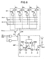
- Figure 6 is a circuit diagram of the configuration of the memory chip MC.
- a memory cell array of 4 rows and 4 columns is explained, but in actuality, the invention can be applied to a memory cell array of m number of rows and n number of columns.
- the memory chip MC has a row decoder RD, a column decoder CD, a memory cell array, and an output circuit.
- memory cells M (M 11 , M 12 ,..., M 34 , M 44 ) are arranged in a matrix form at positions where word lines WL (WL 1 , WL 2 , WL 3 , WL 4 ) connected to the row decoder RD and bit lines BL (BL 1 , BL 2 , BL 3 , BL 4 ) connected to the column decoder CD intersect.
- the memory cells M have access transistors AT (AT 11 , AT 12 ,..., AT 34 , AT 44 ) and insulating film breakage type fuses F (F 11 , F 12 ,..., F 34 , F 44 ).
- the source regions of the access transistors AT (AT 11 , AT 12 ,..., AT 34 , AT 44 ) are connected to the bit lines BL (BL 1 , BL 2 , BL 3 , BL 4 ), and the drain regions are grounded.
- Figure 7 is an equivalent circuit diagram of an example of the configuration of the row decoder RD.
- a voltage V dd is supplied to word lines WL (WL 1 , WL 2 , WL 3 , WL 4 ) selected by OR logic circuits with address data A i (A 0 , A 0 , A 1 , A 1 ...) input thereto or other circuits.
- the row decoder RD may be comprised of only a pass transistor controlled by the address data A i (A 0 , A 0 , A 1 , A 1 ...) and a not illustrated block selection signal ⁇ , and for example the voltage V dd may be supplied to the word line WL selected by the address data and the block selection signal.
- the address data A i (A 0 , A 0 , A 1 , A 1 ...), etc. are supplied from the control chip CC.
- Figure 8 is an equivalent circuit diagram of an example of the configuration of an output system including a column decoder CD and an amplifier.
- memory cell data D M is read from the bit line BL when for example a read signal R obtained from the chip select signal CS and the write enable signal WE becomes ON.
- the column decoder CD may be comprised of only pass transistors controlled by the address data A i (A 16 , A 16 , A 17 , A 17 ...) and the not illustrated block selection signal ⁇ , the input data D IN may be input to the bit line BL selected by the address data and the block selection signal as described above, or the memory cell data D M may be read from the selected bit line BL.
- the address data A i (A 16 , A 16 , A 17 , A 17 ...), block selection signal ⁇ , the input data D IN , etc. are supplied from the control chip CC.
- An amplifier AMP is comprised of for example three current mirror amplifiers (CMA1, CMA2, CMA3). Each current mirror amplifier is comprised of two transistors (Q 1 , Q 2 , Q 3 , Q 4 , Q 5 , Q 6 ).
- the transistors (Q 1 , Q 2 , Q 5 , Q 6 ) are comprised of n-channel MOS transistors (NMOS), while the transistors (Q 3 , Q 4 ) are comprised of p-channel MOS transistors.
- the circuits up to the transistors (Q 1 , Q 2 ) are arranged on the memory chip MC, the transistors (Q 3 , Q 4 , Q 5 , Q 6 ) and following circuits are arranged on the control chip CC, and the transistors (Q 2 , Q 3 ) are connected by a pad PAD.
- a current I a in accordance with the memory cell data D M output from the memory cell array is input to the first current mirror amplifier CMA1
- a current I b amplified in accordance with a ratio of channel widths of the transistors (Q 1 , Q 2 ) comprising the first current mirror amplifier CMA1 flows to the transistor Q 2 side.
- the current I b is amplified to a current I c by a similar operation also in the second current mirror amplifier CMA2, while the current I c is amplified to a current I d in the third current mirror amplifier CMA3.
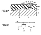
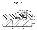
- Figure 9A is a sectional view of the memory cell, while Fig. 9B is a corresponding equivalent circuit diagram.
- a gate insulating film 21 of silicon oxide is formed on the channel forming region in the active region isolated by an element isolation insulating film 20 of a p-type silicon semiconductor substrate 10, and a gate electrode 30a made of polysilicon and acting as the word line WL is formed at an upper layer thereof.
- a source region 11 and a drain region 12 containing n-type impurities with a high concentration are formed in the semiconductor substrate 10 on the two side portions of the gate electrode 30a.
- the n-channel MOS transistor acting as the access transistor AT of the memory cell is comprised as described above.
- a channel length of the transistor is set at for example about 0.1 ⁇ m, and a junction depth of the source and drain region is set at for example about 0.05 ⁇ m.
- a first insulating film 22 of for example silicon oxide is formed over the entire surface covering the n-channel MOS transistor, and a contact hole CH is formed reaching the source region 11.
- a first semiconductor layer 31 made of crystalline silicon formed by epitaxial growth and containing the n-type impurity with a high concentration is formed while connected to the source region 11, a second insulating film 23 of silicon oxide is formed at an upper layer thereof, and a second semiconductor layer 32 made of polysilicon containing the p-type impurity with a high concentration is formed at an upper layer thereof.
- a total thickness of the first semiconductor layer 31, second insulating film 23, and second semiconductor layer 32 is made an extent that does not reach the depth of the contact hole CH.
- an upper layer interconnection 33 made of an aluminum or other metal interconnection and acting as the bit line BL is formed connected to the second semiconductor layer 32.
- drain region 12 is grounded by an interconnection or the like in the semiconductor substrate 10.
- the stack of the first semiconductor layer 31, second insulating film 23, and second semiconductor layer 32 becomes an insulating film breakage type fuse F, that is, a programmable portion.
- insulation breakage in the second insulating film 23 is caused and the first semiconductor layer 31 and the second semiconductor layer 32 are made conductive. Therefore, data can be stored by the conduction or nonconduction between the first semiconductor layer 31 and the second semiconductor layer 32 in each memory cell.
- the conduction between the first semiconductor layer 31 and the second semiconductor layer 32 is confirmed to confirm that the writing succeeds.
- Figure 10 is an energy band diagram for explaining the insulation breakage in the second insulating film 23.
- the influence of the insulation breakage reaches up to the lower portion of the source region at a shallow junction depth, and sometimes becomes the cause of junction leakage, but in the present structure, the influence of the insulation breakage can be prevented from reaching up to the lower portion of the source region by the existence of the first semiconductor layer 31.
- the energy E by the recombination RC of electrons and holes is efficiently transferred to the oxide film, so the reproducibility and the reliability can be improved and thus the insulation breakage in the second insulating film can be caused.
- the thickness of the second insulating film 23 would be a few nanometer thick, and the break down voltage would be around 10 to 15 volt.
- the bit line connected to the memory cell to be read is precharged to a predetermined value
- the word line connected to the memory cell to be similarly read out is made ON to make the access transistor of the related memory cell ON, and the conduction or nonconduction between the first semiconductor layer 31 and the second semiconductor layer 32 in each memory cell is checked according to if the precharge of the bit line fluctuates in potential to thereby obtain the read data.
- the semiconductor nonvolatile memory device (memory chip) according to the present embodiment has a simple configuration where, in the memory cell array, each memory cell has one n-channel MOS transistor (NMOS) and one insulating film breakage type fuse.
- NMOS n-channel MOS transistor
- the semiconductor nonvolatile memory device (memory chip) can be easily and cheaply produced by improving the reproducibility and reliability of the insulating film breakage of the silicon oxide film.
- the PMOS p-channel MOS transistor
- the configuration wherein the row decoder and the column decoder are comprised of only pass transistors (NMOS) or the like it becomes possible to form the memory chip per se by the NMOS process, and it is possible to produce the same while reducing the number of masks to for example about six. Therefore, the manufacturing cost of the memory chip can be greatly reduced.
- control chip per se is originally produced by the COMS process, so the cost will not largely increase.
- the manufacturing cost of the storage medium (memory card) with the built-in memory chip can be reduced.
- an element isolation insulating film 20 is formed on a p-type silicon semiconductor substrate 10 by LOCOS or the like. Further, a conductive impurity is ion-implanted into the active region isolated by the element isolation insulating film 20 for threshold adjustment or the like.
- the surface of the semiconductor substrate 10 is oxidized by for example thermal oxidation to thereby form the gate insulating film 21.
- polysilicon is stacked by CVD (chemical vapor deposition) to form a gate electrode use layer 30.
- CVD chemical vapor deposition
- a resist film R1 of a pattern of the gate electrode is formed by photolithography, etching such as RIE (reactive ion etching) is applied with this resist film R1 as a mask, and the gate electrode use layer 30 and the gate insulating film 21 are patterned to thereby form the gate electrode 30a.
- etching such as RIE (reactive ion etching)
- an n-type conductive impurity is ion-implanted to thereby form the source region 11 and the drain region 12 in the semiconductor substrate 10 on the two sides of the gate electrode 30a.
- NMOS n-channel MOS transistor
- silicon oxide is stacked over the entire surface covering the NMOS by for example CVD to form the first insulating film 22, a resist film R2 of the opening pattern of the contact hole is patterned by photolithography, and etching such as RIE is applied using this resist film R2 as a mask to form the contact hole CH reaching the source region 11.
- the first semiconductor layer 31 containing the n-type conductive impurity with a high concentration is selectively formed in the contact hole CH so as to be connected to the source region 11 by selective epitaxial growth by for example MOCVD (metal organic chemical vapor deposition) process.
- MOCVD metal organic chemical vapor deposition
- the surface layer of the first semiconductor layer 31 is oxidized by for example thermal oxidation, or silicon oxide is stacked by CVD, to thereby form the second insulating film 23.
- the silicon oxide is stacked over the entire surface in the case of CVD, but the illustration of the external portion of the contact hole CH is omitted.
- polysilicon is stacked over the entire surface by for example CVD, a resist film (not illustrated) protecting the contact hole portion is formed by photolithography, and RIE or other etching is applied to eliminate the polysilicon on the outside of the contact hole to thereby form the second semiconductor layer 32 containing the p-type conductive impurity with a high concentration at an upper layer of the second insulating film 23.
- the upper layer interconnection 33 made of the aluminum or other metal interconnection and acting as the bit line is patterned so as to be connected to the second semiconductor layer 32 formed as described above, whereby thus the semiconductor nonvolatile memory device shown in Figs. 9A and 9B is reached.
- the method for production of a semiconductor nonvolatile memory device of the present embodiment it is possible to easily produce the semiconductor nonvolatile memory device according to the present embodiment.
- the reproducibility and reliability are improved, and thus a semiconductor nonvolatile memory device having a memory cell capable of causing insulation breakage in the second insulating film can be produced.
- the device can be formed by the NMOS process, so production is possible while reducing the number of masks to about six, and the manufacturing cost can be suppressed.
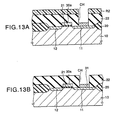
- the p-type silicon semiconductor substrate 10 is isolated by the p + type element isolation region 13 containing the p-type impurity with a high concentration.
- the rest of the configuration is substantially the same as that of the first embodiment.
- the gate insulating film 21 and the gate electrode 30a acting as the word line WL are formed on the channel forming region in the active region isolated by the element isolation region 13, the source region 11 and the drain region 12 are formed in the semiconductor substrate 10 on the two sides of the gate electrode 30a, and thus an n-channel MOS transistor acting as the access transistor AT of the memory cell is comprised.
- a first insulating film 22 of for example silicon oxide is formed over the entire surface while covering the n-channel MOS transistor, the contact hole CH reaching the source region 11 is opened, the first semiconductor layer 31, second insulating film 23, and second semiconductor layer 32 are stacked in the contact hole CH, and an upper layer interconnection 33 made of aluminum or other metal interconnection and acting as the bit line BL is formed while being connected to the second semiconductor layer 32.
- the semiconductor nonvolatile memory device (memory chip) according to the present embodiment has a simple configuration where, in the memory cell array, each memory cell has one n-channel MOS transistor (NMOS) and one insulating film breakage type fuse F, that is, a programmable portion.
- NMOS n-channel MOS transistor
- the semiconductor nonvolatile memory device (memory chip) can be easily and cheaply produced by improving the reproducibility and reliability of the insulating film breakage of the silicon oxide film.
- the semiconductor nonvolatile memory device (memory chip) of the present embodiment in the same way as the first embodiment, it becomes possible to form the memory chip per se by the NMOS process by employing a configuration wherein the row decoder and the column decoder are comprised of only pass transistors (NMOS), and it is possible to produce the same while reducing the number of masks to for example about six. Therefore the manufacturing cost of the memory chip can be greatly reduced.
- NMOS only pass transistors
- the semiconductor nonvolatile memory device (memory chip) according to the present invention embodiment is different in configuration in that, as shown in the equivalent circuit diagram of Fig. 16, in the memory cell array, the source regions of the access transistors AT (AT 11 , AT 12 ,..., AT 34 , AT 44 ) of the memory cells are connected to the bit lines BL (BL 1 , BL 2 , BL 3 , BL 4 ), while the current flowing to the substrate from the drain region is detected as the memory cell output data D M , and connected to the amplifier AMP.
- the rest of the configuration is substantially the same as that of the first embodiment.
- the amplifier AMP receiving the memory cell output data D M is configured comprised of the three current mirror amplifiers (CMA1, CMA2, CMA3) explained in the first embodiment.
- the semiconductor nonvolatile memory device (memory chip) according to the present embodiment has a simple configuration where, in the memory cell array, each memory cell has one n-channel MOS transistor (NMOS) and one insulating film breakage type fuse.
- NMOS n-channel MOS transistor
- the semiconductor nonvolatile memory device (memory chip) can be easily and cheaply produced by improving the reproducibility and reliability of the insulating film breakage of the silicon oxide film.
- the semiconductor nonvolatile memory device (memory chip) of the present embodiment in the same way as the first embodiment, it becomes possible to form the memory chip per se by the NMOS process by employing a configuration wherein the row decoder and the column decoder are comprised of only pass transistors (NMOS), and it is possible to produce the same while reducing the number of masks to for example about six. Therefore the manufacturing cost of the memory chip can be greatly reduced.
- NMOS only pass transistors
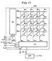
- memory cells M (M 11 , M 12 ,..., M 34 , M 44 ) comprised of insulating film breakage type fuses F (F 11 , F 12 ,..., F 34 , F 44 ) are arranged in a matrix form at positions where the word lines WL (WL 1 , WL 2 , WL 3 , WL 4 ) connected to the row decoder RD and the bit lines BL (BL 1 , BL 2 , BL 3 , BL 4 ) connected to the column decoder CD intersect.
- Figure 18 is an equivalent circuit diagram of an example of the configuration of the row decoder RD.
- the voltage V dd is applied to word lines WL (WL 1 , WL 2 , WL 3 , WL 4 ) selected by OR logic circuits with address data A i (A 0 , A 0 , A 1 , A 1 ...) and selection signal BS ij , etc. input thereto or other circuits.
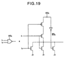
- Figure 19 is an equivalent circuit diagram of the configuration of the OR logic circuit receiving three inputting systems of the address data A i , selection signal BS ij , etc. in the row decoder RD and outputting one system.
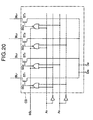
- Figure 20 is an equivalent circuit diagram of an example of the configuration of the column decoder CD.
- the memory cell data D M is read out from the bit line BL when the read signal R becomes ON.
- the OR logic circuit receiving the three inputting systems of the address data A i , the selection signal BS ij , etc. at the column decoder CD and outputting one system is identical to the circuit shown in Fig. 19.
- the amplifier AMP in Fig. 17 can be configured in the same way as that of the amplifier in the first embodiment, that is, can be configured of three current mirror amplifiers each comprised of two transistors. By this, current in accordance with the memory cell data D M can be amplified for example 1000-fold and extracted as the output data.
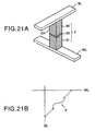
- Figure 21A is a schematic perspective view of a memory cell according to the present embodiment, while Fig. 21B is a corresponding equivalent circuit diagram.
- a not illustrated first insulating film is formed at an upper layer of the first interconnection acting as the word line WL, and a contact hole CH reaching the word line WL is formed.
- the silicon-based first semiconductor layer 31 containing the n-type impurity with a high concentration is formed while being connected to the word line WL, the second insulating film 23 of the silicon oxide is formed at an upper layer thereof, and a silicon-based second semiconductor layer 32 containing the p-type impurity with a high concentration is formed at an upper layer thereof.
- the second interconnection acting as the bit line BL extending in for example a direction orthogonal to the word line WL is formed while being connected to the second semiconductor layer 32.
- the stack of the first semiconductor layer 31, second insulating film 23, and second semiconductor layer 32 becomes the insulating film breakage type fuse F, that is, a programmable portion.
- the insulating film breakage type fuse F that is, a programmable portion.
- the conduction between the first semiconductor layer 31 and the second semiconductor layer 32 is confirmed to confirm if the writing succeeded.
- the conduction or nonconduction between the word line and the bit line connected to the memory cell to be read out is checked to thereby obtain the read data.
- Figure 22 is a circuit diagram of the configuration of a semiconductor nonvolatile memory device wherein a plurality of unit memory cell arrays according to the present embodiment are integrated.
- a plurality of ij-th memory cell arrays MA ij of the above configuration are integrated from (11) to (nm).
- the memory cell data D M is output from each memory cell array MA ij selected by the selection signal BS ij , amplified by the amplifier AMP, and extracted from the D OUT as the output data.
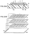
- Figure 23A is a sectional view of a configuration wherein the memory cell arrays according to the present embodiment are integrated in three dimensions to form a memory chip, while Fig. 23B is a schematic view of the stacked configuration thereof.
- the stack of the first interconnection, first insulating film, and second interconnection comprising the unit memory cell array is used as the unit layer, and a plurality of these unit layers (L 1 , L 2 , L 3 , L 4 ,...) are stacked.
- Each of the unit layers (L 1 , L 2 , L 3 , L 4 ,...) is provided with a row decoder and column decoder etc.
- Memory cells comprised of the insulating film breakage type fuses F having the above structure are arranged at intersecting points of the first interconnections and the second interconnections of the unit layers.
- the pads PD are opened in the end portions of the unit layers (L 1 , L 2 , L 3 , L 4 ,...), the memory chip comprising a stack of the unit layers is fixed onto a mount board MB by die bonding or the like, and an electrode EL such as land formed on the mount board MB and the pad Pad of each layer of the memory chip are connected by wire bonding or the like.
- the semiconductor nonvolatile memory device (memory chip) according to the present embodiment has a simple configuration where, in each memory cell array comprising a memory chip, each memory cell has one insulating film breakage type fuse.
- the semiconductor nonvolatile memory device (memory chip) can be easily and cheaply produced by improving the reproducibility and reliability of the insulation breakage of the silicon oxide film.
- substantially the memory chip according to the first embodiment can be similarly formed.
- the first interconnection is formed on the predetermined substrate or the like, the first insulating film is grown at an upper layer thereof, a contact hole reaching the first interconnection is formed, the first semiconductor layer, second insulating film, and second semiconductor layer are stacked in the contact hole, and the second interconnection is formed so as to be connected to the second semiconductor layer, whereby the memory cell array forming the unit layer can be formed.
- a memory chip comprised of unit memory cell arrays stacked therein can be formed.
- the memory chip formed as described above is used by opening the pad for every unit and mounting it on the mount board.
- the semiconductor nonvolatile memory device (memory chip) according to the present embodiment makes the access transistor a TFT (thin film transistor) as shown in the sectional view of Fig. 24.
- a gate insulating film 21 of silicon oxide is formed on a channel forming region in an active region isolated by an element isolation region 10c of a semiconductor layer (also referred to as the SOI layer) 10b having an SOI (semiconductor on insulator) structure formed on an insulating substrate 10a obtained by covering a glass substrate or the surface layer by an insulator such as silicon oxide.
- a gate electrode 30a made of polysilicon and acting as the word line WL is formed at an upper layer thereof.
- a source region 11 and a drain region 12 containing the n-type impurities with a high concentration are formed in the SOI layer 10b on the two sides of the gate electrode 30a.
- An n-channel MOS transistor having an TFT structure acting as the access transistor of the memory cell is comprised as described above.
- the SOI layer 10b is formed with a thickness of for example about 1 ⁇ m, and the insulating substrate 10a is formed with a thickness of about several to several hundred ⁇ m.
- the channel length of the transistor is determined to about 0.1 ⁇ m in the same way as the first embodiment, and a complete depletion type transistor can be obtained wherein the source and drain regions have depths reaching the bottom surface of the SOI layer 10b.
- a first insulating film 22 of for example silicon oxide is formed over the entire surface while covering the n-channel MOS transistor, a contact hole CH reaching the source region 11 is formed, a second insulating film 23 and an semiconductor layer 32 containing the p-type impurity with a high concentration are stacked in the contact hole CH, and an upper layer interconnection 33 made of aluminum or another metal interconnection and acting as the bit line BL is formed while connected to the semiconductor layer 32.
- the junction depth of the source region is shallow, so the first semiconductor layer 31 was required for preventing the influence of the insulation breakage from reaching the lower portion of the source region, but junction leakage is not caused in an TFT having the above structure. Therefore, a configuration of directly stacking the second insulating film 23 and the semiconductor layer 32 containing the p-type impurity with a high concentration on the source region can be employed.
- the energy E by the recombination RC of electrons and holes is efficiently transferred to the oxide film, therefore the reproducibility and reliability are improved and thus insulation breakage in the second insulating film is caused.
- the semiconductor nonvolatile memory device (memory chip) according to the present embodiment has a simple configuration where each of memory cells comprising the memory cell array has one n-channel MOS transistor (NMOS) and one insulating film breakage type fuse F, that is, a programmable portion.
- NMOS n-channel MOS transistor
- the semiconductor nonvolatile memory device (memory chip) can be easily and cheaply produced by improving the reproducibility and reliability of insulation breakage of the silicon oxide film.
- the semiconductor nonvolatile memory device (memory chip) of the present embodiment in combination with the control chip as shown in Fig. 5, the PMOS's (p-channel MOS transistor) required for the circuit configuration of the decoder, amplifier, etc. can be provided not on the memory chip, but on the control chip. Namely, by employing the configuration wherein the row decoder and the column decoder are comprised of only pass transistors (NMOS), etc., it becomes possible to form the memory chip per se by the NMOS process, and it is possible to produce the same while reducing the number of masks to for example about six. Therefore, the manufacturing cost of the memory chip can be greatly reduced.
- NMOS pass transistors
- control chip per se is originally produced by the CMOS process, so the cost will not largely increase.
- the manufacturing cost of the storage medium (memory card) with the built-in memory chip can be lowered.
- the SOI structure layers (L 1 , L 2 , L 3 , L 4 ,...) comprised of insulating layers and semiconductor layers formed at the upper layers thereof as unit layers, and stacking a plurality of unit layers in the same way as the stack shown in Figs. 23A and 23B according to the fourth embodiment, integration in three-dimensional directions can be achieved.
- the insulating layer in this case is made of for example a silicon oxide layer formed by CVD and has a thickness thereof determined to about 10 ⁇ m.
- a memory cell array wherein the memory cells each being comprised of the TFT of above structure and the insulation breakage type fuse are arranged in the SOI layer in a matrix form, and a row decoder and column decoder tc. made of for example pass transistors are formed.
- the pads PAD are opened in the end portions of the layers of the SOI structure layers (L 1 , L 2 , L 3 , L 4 ,).
- the memory chip of the stack of the SOI structure layers (L 1 , L 2 , L 3 , L 4 , ...) is fixed to the mount board MB by die bonding or the like, and the electrodes EL such as lands formed on the mount board MB and the pad PAD of each layer of memory chip are connected by wire bonding or the like.
- the manufacturing cost per unit storage capacity can be reduced to about 1/N, so the effect of reduction of cost can be further increased.
- a memory cell comprised of only the insulation breakage type fuse as in the fourth embodiment can be formed.
- the SOI structure layer having the memory cells comprised of insulation breakage type fuses can be stacked as described above too.
- the present invention is not limited to the above embodiments.
- the row decoder, column decoder, amplifier, etc. are not limited to the configuration comprised of only NMOS transistors, but can be formed by the CMOS process including inverters or the like too.
- LDD structures As the source and drain region of the access transistor, various structures such as LDD structures can be employed.
- the reproducibility and reliability are improved, thus insulation breakage in the second insulating film can be caused.
- the memory cell can be comprised by a simple structure, by making for example the row decoder and column decoder by only pass transistors, it is possible to produce the device while reducing the number of masks, and it is possible to suppress the manufacturing cost.
- a semiconductor nonvolatile memory device of the present invention it is possible to produce a semiconductor nonvolatile memory device having a memory cell capable of improving the reproducibility and reliability and causing insulation breakage in the second insulating film while reducing the number of masks, and the manufacturing cost can be suppressed.
Landscapes
- Semiconductor Memories (AREA)
- Non-Volatile Memory (AREA)
- Read Only Memory (AREA)
- Design And Manufacture Of Integrated Circuits (AREA)
Claims (12)
- Nichtflüchtige Halbleiterspeichervorrichtung mit wenigstens einer Speicherzelle, wobei die Speicherzelle aufweist:dadurch gekennzeichnet, dass der Programmabschnitt eine erste Halbleiterschicht (31) des ersten Leitungstyps, einen zweiten Isolierfilm (23) und eine zweite Halbleiterschicht (32) eines zweiten Leitungstyps aufweist, wobei die erste Halbleiterschicht, der zweite Isolierfilm und die zweite Halbleiterschicht nacheinander in der Öffnung gestapelt sind, die erste Halbleiterschicht auf dem Störstellenbereich gebildet ist, und der zweite Isolierfilm in einem Leitungszustand als Reaktion auf Programmdaten verändert ist, um dadurch eine elektrische Verbindung zwischen der ersten und der zweiten Halbleiterschicht herzustellen.einen Störstellenbereich (11) eines ersten Leitungstyps, der in einem Halbleitersubstrat (10) gebildet ist;einem ersten Isolierfilm (22), der auf dem Halbleitersubstrat (10) über dem Störstellenbereich (11) gebildet ist;einer Öffnung (CH), die in dem ersten Isolierfilm (22) so gebildet ist, dass sie bis zu dem Störstellenbereich (11) reicht; undeinem Programmabschnitt,
- Nichtflüchtige Halbleiterspeichervorrichtung nach Anspruch 1, bei welcher in der Speicherzelle eine als Wortleitung (WL) dienende Gate-Elektrode (30a) über einen Gate-Isolierfilm (21) auf dem Halbleitersubstrat (10) gebildet ist, ein Kanalbildungsbereich auf dem Halbleitersubstrat unter der Gate-Elektrode vorgesehen ist, und ein den Störstellenbereich als Drain-Bereich (12) verwendender Feldeffekttransistor gebildet ist; und eine Bitleitung (33) mit der zweiten Halbleiterschicht (32) verbunden ist.
- Nichtflüchtige Halbleiterspeichervorrichtung nach Anspruch 1 oder 2, bei welcher in dem zweiten Isolierfilm in dem Programmabschnitt durch Anlegen einer vorbestimmten Spannung zwischen der ersten Halbleiterschicht und der zweiten Halbleiterschicht als Reaktion auf die in der Speicherzelle zu speichernden Programmdaten ein Isolationsdurchbruch bewirkt ist; und in jeder Speicherzelle Daten durch die Leitung oder Nicht-Leitung zwischen der ersten Halbleiterschicht und der zweiten Halbleiterschicht gespeichert sind.
- Nichtflüchtige Halbleiterspeichervorrichtung nach Anspruch 2, bei welcher der Source-Bereich des Feldeffekttransistors geerdet ist.
- Nichtflüchtige Halbleiterspeichervorrichtung nach Anspruch 2, ferner mit einer Einrichtung zum Erfassen eines von dem Source-Bereich des Feldeffekttransistors zu der Halbleitersubstratseite fließenden Stroms.
- Nichtflüchtige Halbleiterspeichervorrichtung nach Anspruch 2, bei welcher die Wortleitung und die Bitleitung mit einem Zeilendecodierer und einem Spaltendecodierer mit Durchgangstransistoren zum Hindurchlassen zugeführter Signale verbunden sind.
- Nichtflüchtige Halbleiterspeichervorrichtung nach Anspruch 6, bei welcher invertierte Signale von Adresssignalen dem Zeilendecodierer und dem Spalten decodierer von einer externen Vorrichtung zusammen mit Vorwärtssignalen zugeführt werden.
- Nichtflüchtige Halbleiterspeichervorrichtung nach Anspruch 1, bei welcher die mehreren Speicherzellen in Matrixform angeordnet sind.
- Verfahren zur Herstellung einer nichtflüchtigen Halbleiterspeichervorrichtung
mit wenigstens einer Speicherzelle, wobei ein Prozess zum Bilden der Speicherzelle die Schritte enthält:dadurch gekennzeichnet, dass der Prozess des Bildens der Speicherzelle ferner die Schritte enthält;Bilden eines Störstellenbereichs eines ersten Leitungstyps in einem Halbleitersubstrat;Bilden eines ersten Isolierfilms auf dem Halbleitersubstrat über dem Störstellenbereich;Bilden einer Öffnung in dem ersten Isolierfilm so, dass sie bis zu dem Störstellenbereich reicht,
Bilden einer ersten Halbleiterschicht eines ersten Leitungstyps auf dem Störstellenbereich in der Öffnung;
Bilden eines zweiten Isolierfilms auf der ersten Halbleiterschicht in der Öffnung; und
Bilden einer zweiten Halbleiterschicht eines zweiten Leitungstyps auf dem zweiten Isolierfilm in der Öffnung. - Verfahren zur Herstellung einer nichtflüchtigen Halbleiterspeichervorrichtung nach Anspruch 9, bei welchem der Schritt des Bildens der ersten Halbleiterschicht ein Schritt des Bildens derselben durch ein selektives epitaktisches Wachsen ist.
- Verfahren zur Herstellung einer nichtflüchtigen Halbleiterspeichervorrichtung nach Anspruch 9, bei welchem
ein Schritt des Bildens einer als Wortleitung dienenden Gate-Elektrode über einem Gate-Isolierfilm auf dem als Kanalbildungsbereich dienenden Halbleitersubstrat vor dem Schritt des Bildens des Störstellenbereichs des ersten Leitungstyps auf dem Halbleitersubstrat vorgesehen ist;
in dem Schritt des Bildens des Störstellenbereichs des ersten Leitungstyps auf dem Halbleitersubstrat in dem Halbleitersubstrat auf beiden Seitenabschnitten der Gate-Elektrode ein Source-Bereich und ein Drain-Bereich, die als der Störstellenbereich dienen, gebildet werden; und
ferner ein Schritt des Bildens einer Bitleitung an einer oberen Schicht der zweiten Halbleiterschicht vorgesehen ist. - Verfahren zur Herstellung einer nichtflüchtigen Halbleiterspeichervorrichtung nach Anspruch 11, bei welchem der Zeilendecodierer und der Spaltendecodierer, die mit der Wortleitung und der Bitleitung verbunden sind, nur durch Durchgangstransistoren gebildet werden.
Applications Claiming Priority (2)
| Application Number | Priority Date | Filing Date | Title |
|---|---|---|---|
| JP2001027307A JP3846202B2 (ja) | 2001-02-02 | 2001-02-02 | 半導体不揮発性記憶装置 |
| JP2001027307 | 2001-02-02 |
Publications (2)
| Publication Number | Publication Date |
|---|---|
| EP1229552A1 EP1229552A1 (de) | 2002-08-07 |
| EP1229552B1 true EP1229552B1 (de) | 2005-04-06 |
Family
ID=18891994
Family Applications (1)
| Application Number | Title | Priority Date | Filing Date |
|---|---|---|---|
| EP20010401707 Expired - Lifetime EP1229552B1 (de) | 2001-02-02 | 2001-06-27 | Einmalig programmierbare nichtflüchtige halbleiterspeicheranordnung und verfahren zu deren herstellung |
Country Status (7)
| Country | Link |
|---|---|
| US (2) | US6583490B2 (de) |
| EP (1) | EP1229552B1 (de) |
| JP (1) | JP3846202B2 (de) |
| KR (1) | KR100791905B1 (de) |
| CN (1) | CN1157792C (de) |
| DE (1) | DE60109887T2 (de) |
| TW (1) | TW517233B (de) |
Families Citing this family (27)
| Publication number | Priority date | Publication date | Assignee | Title |
|---|---|---|---|---|
| US20030109125A1 (en) * | 2001-12-10 | 2003-06-12 | Chewnpu Jou | Fuse structure for a semiconductor device and manufacturing method thereof |
| US6727145B1 (en) * | 2002-12-26 | 2004-04-27 | Megawin Technology Co., Ltd. | Method for fabricating post-process one-time programmable read only memory cell |
| US6911360B2 (en) * | 2003-04-29 | 2005-06-28 | Freescale Semiconductor, Inc. | Fuse and method for forming |
| US7132350B2 (en) | 2003-07-21 | 2006-11-07 | Macronix International Co., Ltd. | Method for manufacturing a programmable eraseless memory |
| US7281274B2 (en) * | 2003-10-16 | 2007-10-09 | Lmp Media Llc | Electronic media distribution system |
| KR100546392B1 (ko) | 2003-11-01 | 2006-01-26 | 삼성전자주식회사 | Eprom 소자를 포함하는 반도체 소자와 그 제조 방법 |
| CN100573569C (zh) | 2004-09-10 | 2009-12-23 | 株式会社半导体能源研究所 | 半导体装置 |
| JP2006148088A (ja) * | 2004-10-22 | 2006-06-08 | Semiconductor Energy Lab Co Ltd | 半導体装置 |
| US7935958B2 (en) | 2004-10-22 | 2011-05-03 | Semiconductor Energy Laboratory Co., Ltd. | Semiconductor device |
| US7242072B2 (en) * | 2004-11-23 | 2007-07-10 | International Business Machines Corporation | Electrically programmable fuse for silicon-on-insulator (SOI) technology |
| JP4749162B2 (ja) * | 2005-01-31 | 2011-08-17 | 株式会社半導体エネルギー研究所 | 半導体装置 |
| US7768014B2 (en) | 2005-01-31 | 2010-08-03 | Semiconductor Energy Laboratory Co., Ltd. | Memory device and manufacturing method thereof |
| US8604547B2 (en) | 2005-02-10 | 2013-12-10 | Semiconductor Energy Laboratory Co., Ltd. | Memory element and semiconductor device |
| US7926726B2 (en) * | 2005-03-28 | 2011-04-19 | Semiconductor Energy Laboratory Co., Ltd. | Survey method and survey system |
| CN100391002C (zh) * | 2005-03-29 | 2008-05-28 | 旺宏电子股份有限公司 | 单次可程序化只读存储器及其制造方法 |
| JP5190182B2 (ja) * | 2005-05-31 | 2013-04-24 | 株式会社半導体エネルギー研究所 | 半導体装置 |
| WO2006129739A1 (en) | 2005-05-31 | 2006-12-07 | Semiconductor Energy Laboratory Co., Ltd. | Semiconductor device |
| KR100667461B1 (ko) * | 2005-09-26 | 2007-01-10 | 리디스 테크놀로지 인코포레이티드 | 각 셀의 소스 영역마다 콘택이 형성되어 있는 오티피 롬 셀구조, 및 상기 롬의 프로그래밍 및 읽기 방법 |
| CN100442524C (zh) * | 2005-09-28 | 2008-12-10 | 中芯国际集成电路制造(上海)有限公司 | 用于嵌入式eeprom中的一次可编程存储器器件的结构与方法 |
| JP5027470B2 (ja) * | 2005-09-29 | 2012-09-19 | 株式会社半導体エネルギー研究所 | 記憶装置 |
| TWI411095B (zh) * | 2005-09-29 | 2013-10-01 | 半導體能源研究所股份有限公司 | 記憶裝置 |
| KR100875165B1 (ko) * | 2007-07-04 | 2008-12-22 | 주식회사 동부하이텍 | 반도체 소자 및 제조 방법 |
| CN101527167B (zh) * | 2008-02-01 | 2012-08-15 | 索尼株式会社 | 显示装置 |
| JP4596070B2 (ja) * | 2008-02-01 | 2010-12-08 | ソニー株式会社 | メモリ素子及びメモリ素子の製造方法、並びに表示装置及び表示装置の製造方法 |
| KR100979098B1 (ko) | 2008-06-20 | 2010-08-31 | 주식회사 동부하이텍 | 반도체 소자 및 이를 위한 otp 셀 형성 방법 |
| JP6345107B2 (ja) * | 2014-12-25 | 2018-06-20 | ルネサスエレクトロニクス株式会社 | 半導体装置およびその製造方法 |
| CN108538880B (zh) * | 2017-03-02 | 2020-11-10 | 旺宏电子股份有限公司 | 半导体元件及具有此半导体元件的装置 |
Family Cites Families (36)
| Publication number | Priority date | Publication date | Assignee | Title |
|---|---|---|---|---|
| US2559020A (en) * | 1948-12-18 | 1951-07-03 | Lehmkuhl Joakim | Ski binding |
| US3386748A (en) * | 1966-04-01 | 1968-06-04 | Eie Nils | Ski fastening |
| US3504922A (en) * | 1968-04-09 | 1970-04-07 | Philip K Wiley | Tension adjustable releasable ski bindings |
| US3730543A (en) * | 1971-01-08 | 1973-05-01 | J Edmund | Safety ski binding |
| US3787868A (en) * | 1971-06-25 | 1974-01-22 | J Camp | Remotely actuated release apparatus for ski bindings |
| US4023824A (en) * | 1972-06-15 | 1977-05-17 | Von Besser Kurt | Ski binding apparatus |
| US3874685A (en) * | 1972-06-15 | 1975-04-01 | Besser Kurt Von | Ski binding apparatus and method of mounting |
| FR2214496B1 (de) * | 1973-01-19 | 1976-11-05 | Salomon Georges P J | |
| US4058326A (en) * | 1974-06-07 | 1977-11-15 | Antonio Faulin | Ski bindings |
| US4033604A (en) * | 1975-08-21 | 1977-07-05 | Cirino John F | Release assembly for ski binding |
| FI771004A7 (de) * | 1976-04-06 | 1977-10-07 | Witco As | |
| DE2707626C2 (de) * | 1977-02-23 | 1985-11-14 | Geze Gmbh, 7250 Leonberg | Langlaufbindung |
| JPS5688357A (en) | 1979-12-21 | 1981-07-17 | Fujitsu Ltd | Selectively writable semiconductor element |
| US4322090A (en) * | 1980-02-13 | 1982-03-30 | Loughney Charles E | Ski mountaineering binding |
| US4533156A (en) * | 1980-12-30 | 1985-08-06 | Tmc Corporation | Toe mechanism for a safety ski binding |
| JPS5828750A (ja) | 1981-08-12 | 1983-02-19 | Canon Inc | 光導電部材 |
| JPH073855B2 (ja) | 1985-07-26 | 1995-01-18 | 富士通株式会社 | 半導体装置の製造方法 |
| US4899205A (en) | 1986-05-09 | 1990-02-06 | Actel Corporation | Electrically-programmable low-impedance anti-fuse element |
| JPS632207A (ja) | 1986-06-20 | 1988-01-07 | 古河電気工業株式会社 | Ofケ−ブルの処理方法 |
| DE3808643C2 (de) * | 1987-11-27 | 1994-04-28 | Implementors Overseas Ltd | Selbsttätig auslösbare Skibindungseinheit |
| JPH01235374A (ja) | 1988-03-16 | 1989-09-20 | Fujitsu Ltd | 半導体記憶装置 |
| FR2638974B1 (fr) * | 1988-08-16 | 1990-09-21 | Salomon Sa | Fixation de ski de fond de type charniere |
| JPH0831563B2 (ja) | 1989-06-16 | 1996-03-27 | 松下電子工業株式会社 | プログラマブル素子の製造方法 |
| DE4007667C1 (de) * | 1990-03-10 | 1991-06-20 | Silvretta - Sherpas Sportartikel Gmbh & Co Kg, 8047 Karlsfeld, De | |
| US5066036A (en) * | 1990-03-19 | 1991-11-19 | Broughton Timothy C | Ski binding |
| JP2829664B2 (ja) | 1990-04-27 | 1998-11-25 | 株式会社スリーボンド | 含ケイ素α−シアノアクリレートの製造法 |
| US5383365A (en) * | 1992-09-17 | 1995-01-24 | The Babcock & Wilcox Company | Crack orientation determination and detection using horizontally polarized shear waves |
| JPH07263647A (ja) * | 1994-02-04 | 1995-10-13 | Canon Inc | 電子回路装置 |
| DE59602385D1 (de) * | 1995-02-02 | 1999-08-12 | Rottefella As | Kombination einer skibindung und eines daran angepassten schuhs |
| US5751012A (en) * | 1995-06-07 | 1998-05-12 | Micron Technology, Inc. | Polysilicon pillar diode for use in a non-volatile memory cell |
| US5789277A (en) * | 1996-07-22 | 1998-08-04 | Micron Technology, Inc. | Method of making chalogenide memory device |
| JP3215345B2 (ja) * | 1997-03-19 | 2001-10-02 | 富士通株式会社 | 半導体装置の製造方法 |
| JPH10341000A (ja) | 1997-04-11 | 1998-12-22 | Citizen Watch Co Ltd | 半導体不揮発性記憶装置およびその製造方法 |
| US6034882A (en) | 1998-11-16 | 2000-03-07 | Matrix Semiconductor, Inc. | Vertically stacked field programmable nonvolatile memory and method of fabrication |
| JP4068746B2 (ja) * | 1998-12-25 | 2008-03-26 | 株式会社ルネサステクノロジ | 半導体集積回路装置 |
| JP3743189B2 (ja) * | 1999-01-27 | 2006-02-08 | 富士通株式会社 | 不揮発性半導体記憶装置及びその製造方法 |
-
2001
- 2001-02-02 JP JP2001027307A patent/JP3846202B2/ja not_active Expired - Lifetime
- 2001-05-14 KR KR20010026184A patent/KR100791905B1/ko not_active Expired - Lifetime
- 2001-06-01 TW TW90113368A patent/TW517233B/zh not_active IP Right Cessation
- 2001-06-26 US US09/888,534 patent/US6583490B2/en not_active Expired - Lifetime
- 2001-06-27 EP EP20010401707 patent/EP1229552B1/de not_active Expired - Lifetime
- 2001-06-27 CN CNB011254823A patent/CN1157792C/zh not_active Expired - Lifetime
- 2001-06-27 DE DE2001609887 patent/DE60109887T2/de not_active Expired - Lifetime
-
2003
- 2003-02-14 US US10/366,564 patent/US6800527B2/en not_active Expired - Lifetime
Also Published As
| Publication number | Publication date |
|---|---|
| KR100791905B1 (ko) | 2008-01-07 |
| EP1229552A1 (de) | 2002-08-07 |
| CN1157792C (zh) | 2004-07-14 |
| TW517233B (en) | 2003-01-11 |
| JP3846202B2 (ja) | 2006-11-15 |
| DE60109887T2 (de) | 2006-02-23 |
| JP2002231899A (ja) | 2002-08-16 |
| US6583490B2 (en) | 2003-06-24 |
| US20030146467A1 (en) | 2003-08-07 |
| US20020105050A1 (en) | 2002-08-08 |
| US6800527B2 (en) | 2004-10-05 |
| CN1368763A (zh) | 2002-09-11 |
| DE60109887D1 (de) | 2005-05-12 |
| KR20020064627A (ko) | 2002-08-09 |
Similar Documents
| Publication | Publication Date | Title |
|---|---|---|
| EP1229552B1 (de) | Einmalig programmierbare nichtflüchtige halbleiterspeicheranordnung und verfahren zu deren herstellung | |
| US11211372B2 (en) | Semiconductor device | |
| US11515413B2 (en) | 3D semiconductor device and structure with memory | |
| KR100549475B1 (ko) | 반도체 집적 회로 장치 및 반도체 집적 회로 장치의 제조방법 | |
| KR100423896B1 (ko) | 축소가능한 2개의 트랜지스터 기억 소자 | |
| JP4565767B2 (ja) | 不揮発性半導体記憶装置 | |
| US8679917B2 (en) | Buried bit line anti-fuse one-time-programmable nonvolatile memory | |
| KR960012252B1 (ko) | 반도체 메모리장치 | |
| KR100712089B1 (ko) | 반도체메모리장치 및 그 제조방법 | |
| US10325651B2 (en) | 3D semiconductor device with stacked memory | |
| US6078074A (en) | Semiconductor device having multilayer metal interconnection | |
| CN1954432A (zh) | 用于快闪存储装置中保护字线的方法及装置 | |
| US6642574B2 (en) | Semiconductor memory device and manufacturing method thereof | |
| JP6623247B2 (ja) | フラッシュメモリおよびその製造方法 | |
| US20080029826A1 (en) | Semicondutor memory device and method of manufacturing the same | |
| JP3226589B2 (ja) | 不揮発性半導体記憶装置の製造方法 | |
| JP3940477B2 (ja) | 半導体装置 | |
| TWI913462B (zh) | 半導體記憶體裝置及系統與製造半導體記憶體裝置的方法 | |
| TW202503743A (zh) | 具鰭式場效電晶體之反熔絲型記憶體 |
Legal Events
| Date | Code | Title | Description |
|---|---|---|---|
| PUAI | Public reference made under article 153(3) epc to a published international application that has entered the european phase |
Free format text: ORIGINAL CODE: 0009012 |
|
| AK | Designated contracting states |
Kind code of ref document: A1 Designated state(s): AT BE CH CY DE DK ES FI FR GB GR IE IT LI LU MC NL PT SE TR |
|
| AX | Request for extension of the european patent |
Free format text: AL;LT;LV;MK;RO;SI |
|
| 17P | Request for examination filed |
Effective date: 20030130 |
|
| AKX | Designation fees paid |
Designated state(s): DE FR GB |
|
| 17Q | First examination report despatched |
Effective date: 20030505 |
|
| GRAP | Despatch of communication of intention to grant a patent |
Free format text: ORIGINAL CODE: EPIDOSNIGR1 |
|
| GRAS | Grant fee paid |
Free format text: ORIGINAL CODE: EPIDOSNIGR3 |
|
| GRAA | (expected) grant |
Free format text: ORIGINAL CODE: 0009210 |
|
| AK | Designated contracting states |
Kind code of ref document: B1 Designated state(s): DE FR GB |
|
| REG | Reference to a national code |
Ref country code: GB Ref legal event code: FG4D |
|
| REG | Reference to a national code |
Ref country code: IE Ref legal event code: FG4D |
|
| REF | Corresponds to: |
Ref document number: 60109887 Country of ref document: DE Date of ref document: 20050512 Kind code of ref document: P |
|
| PLBE | No opposition filed within time limit |
Free format text: ORIGINAL CODE: 0009261 |
|
| STAA | Information on the status of an ep patent application or granted ep patent |
Free format text: STATUS: NO OPPOSITION FILED WITHIN TIME LIMIT |
|
| ET | Fr: translation filed | ||
| 26N | No opposition filed |
Effective date: 20060110 |
|
| REG | Reference to a national code |
Ref country code: GB Ref legal event code: 746 Effective date: 20120702 |
|
| REG | Reference to a national code |
Ref country code: DE Ref legal event code: R084 Ref document number: 60109887 Country of ref document: DE Effective date: 20120614 |
|
| REG | Reference to a national code |
Ref country code: FR Ref legal event code: PLFP Year of fee payment: 16 |
|
| REG | Reference to a national code |
Ref country code: DE Ref legal event code: R082 Ref document number: 60109887 Country of ref document: DE Representative=s name: MITSCHERLICH, PATENT- UND RECHTSANWAELTE PARTM, DE Ref country code: DE Ref legal event code: R081 Ref document number: 60109887 Country of ref document: DE Owner name: SONY SEMICONDUCTOR SOLUTIONS CORP., ATSUGI-SHI, JP Free format text: FORMER OWNER: SONY CORPORATION, TOKIO/TOKYO, JP |
|
| REG | Reference to a national code |
Ref country code: GB Ref legal event code: 732E Free format text: REGISTERED BETWEEN 20170105 AND 20170111 |
|
| REG | Reference to a national code |
Ref country code: FR Ref legal event code: TP Owner name: SONY SEMICONDUCTOR SOLUTIONS CORPORATION, JP Effective date: 20170124 |
|
| REG | Reference to a national code |
Ref country code: FR Ref legal event code: PLFP Year of fee payment: 17 |
|
| REG | Reference to a national code |
Ref country code: FR Ref legal event code: PLFP Year of fee payment: 18 |
|
| PGFP | Annual fee paid to national office [announced via postgrant information from national office to epo] |
Ref country code: DE Payment date: 20200618 Year of fee payment: 20 Ref country code: FR Payment date: 20200619 Year of fee payment: 20 |
|
| PGFP | Annual fee paid to national office [announced via postgrant information from national office to epo] |
Ref country code: GB Payment date: 20200625 Year of fee payment: 20 |
|
| REG | Reference to a national code |
Ref country code: DE Ref legal event code: R071 Ref document number: 60109887 Country of ref document: DE |
|
| REG | Reference to a national code |
Ref country code: GB Ref legal event code: PE20 Expiry date: 20210626 |
|
| PG25 | Lapsed in a contracting state [announced via postgrant information from national office to epo] |
Ref country code: GB Free format text: LAPSE BECAUSE OF EXPIRATION OF PROTECTION Effective date: 20210626 |