EP1164641B1 - Light emitting module and method of driving the same, and optical sensor - Google Patents
Light emitting module and method of driving the same, and optical sensor Download PDFInfo
- Publication number
- EP1164641B1 EP1164641B1 EP01114266A EP01114266A EP1164641B1 EP 1164641 B1 EP1164641 B1 EP 1164641B1 EP 01114266 A EP01114266 A EP 01114266A EP 01114266 A EP01114266 A EP 01114266A EP 1164641 B1 EP1164641 B1 EP 1164641B1
- Authority
- EP
- European Patent Office
- Prior art keywords
- light emitting
- emitting module
- tft
- section
- sensor
- Prior art date
- Legal status (The legal status is an assumption and is not a legal conclusion. Google has not performed a legal analysis and makes no representation as to the accuracy of the status listed.)
- Expired - Lifetime
Links
Images


Classifications
-
- H—ELECTRICITY
- H10—SEMICONDUCTOR DEVICES; ELECTRIC SOLID-STATE DEVICES NOT OTHERWISE PROVIDED FOR
- H10D—INORGANIC ELECTRIC SEMICONDUCTOR DEVICES
- H10D86/00—Integrated devices formed in or on insulating or conducting substrates, e.g. formed in silicon-on-insulator [SOI] substrates or on stainless steel or glass substrates
- H10D86/01—Manufacture or treatment
- H10D86/021—Manufacture or treatment of multiple TFTs
- H10D86/0231—Manufacture or treatment of multiple TFTs using masks, e.g. half-tone masks
-
- G—PHYSICS
- G09—EDUCATION; CRYPTOGRAPHY; DISPLAY; ADVERTISING; SEALS
- G09G—ARRANGEMENTS OR CIRCUITS FOR CONTROL OF INDICATING DEVICES USING STATIC MEANS TO PRESENT VARIABLE INFORMATION
- G09G3/00—Control arrangements or circuits, of interest only in connection with visual indicators other than cathode-ray tubes
- G09G3/20—Control arrangements or circuits, of interest only in connection with visual indicators other than cathode-ray tubes for presentation of an assembly of a number of characters, e.g. a page, by composing the assembly by combination of individual elements arranged in a matrix no fixed position being assigned to or needed to be assigned to the individual characters or partial characters
- G09G3/22—Control arrangements or circuits, of interest only in connection with visual indicators other than cathode-ray tubes for presentation of an assembly of a number of characters, e.g. a page, by composing the assembly by combination of individual elements arranged in a matrix no fixed position being assigned to or needed to be assigned to the individual characters or partial characters using controlled light sources
- G09G3/30—Control arrangements or circuits, of interest only in connection with visual indicators other than cathode-ray tubes for presentation of an assembly of a number of characters, e.g. a page, by composing the assembly by combination of individual elements arranged in a matrix no fixed position being assigned to or needed to be assigned to the individual characters or partial characters using controlled light sources using electroluminescent panels
-
- G—PHYSICS
- G01—MEASURING; TESTING
- G01J—MEASUREMENT OF INTENSITY, VELOCITY, SPECTRAL CONTENT, POLARISATION, PHASE OR PULSE CHARACTERISTICS OF INFRARED, VISIBLE OR ULTRAVIOLET LIGHT; COLORIMETRY; RADIATION PYROMETRY
- G01J1/00—Photometry, e.g. photographic exposure meter
- G01J1/42—Photometry, e.g. photographic exposure meter using electric radiation detectors
- G01J1/4204—Photometry, e.g. photographic exposure meter using electric radiation detectors with determination of ambient light
-
- G—PHYSICS
- G01—MEASURING; TESTING
- G01J—MEASUREMENT OF INTENSITY, VELOCITY, SPECTRAL CONTENT, POLARISATION, PHASE OR PULSE CHARACTERISTICS OF INFRARED, VISIBLE OR ULTRAVIOLET LIGHT; COLORIMETRY; RADIATION PYROMETRY
- G01J1/00—Photometry, e.g. photographic exposure meter
- G01J1/42—Photometry, e.g. photographic exposure meter using electric radiation detectors
- G01J1/44—Electric circuits
-
- G—PHYSICS
- G09—EDUCATION; CRYPTOGRAPHY; DISPLAY; ADVERTISING; SEALS
- G09G—ARRANGEMENTS OR CIRCUITS FOR CONTROL OF INDICATING DEVICES USING STATIC MEANS TO PRESENT VARIABLE INFORMATION
- G09G3/00—Control arrangements or circuits, of interest only in connection with visual indicators other than cathode-ray tubes
- G09G3/20—Control arrangements or circuits, of interest only in connection with visual indicators other than cathode-ray tubes for presentation of an assembly of a number of characters, e.g. a page, by composing the assembly by combination of individual elements arranged in a matrix no fixed position being assigned to or needed to be assigned to the individual characters or partial characters
- G09G3/22—Control arrangements or circuits, of interest only in connection with visual indicators other than cathode-ray tubes for presentation of an assembly of a number of characters, e.g. a page, by composing the assembly by combination of individual elements arranged in a matrix no fixed position being assigned to or needed to be assigned to the individual characters or partial characters using controlled light sources
- G09G3/30—Control arrangements or circuits, of interest only in connection with visual indicators other than cathode-ray tubes for presentation of an assembly of a number of characters, e.g. a page, by composing the assembly by combination of individual elements arranged in a matrix no fixed position being assigned to or needed to be assigned to the individual characters or partial characters using controlled light sources using electroluminescent panels
- G09G3/32—Control arrangements or circuits, of interest only in connection with visual indicators other than cathode-ray tubes for presentation of an assembly of a number of characters, e.g. a page, by composing the assembly by combination of individual elements arranged in a matrix no fixed position being assigned to or needed to be assigned to the individual characters or partial characters using controlled light sources using electroluminescent panels semiconductive, e.g. using light-emitting diodes [LED]
- G09G3/3208—Control arrangements or circuits, of interest only in connection with visual indicators other than cathode-ray tubes for presentation of an assembly of a number of characters, e.g. a page, by composing the assembly by combination of individual elements arranged in a matrix no fixed position being assigned to or needed to be assigned to the individual characters or partial characters using controlled light sources using electroluminescent panels semiconductive, e.g. using light-emitting diodes [LED] organic, e.g. using organic light-emitting diodes [OLED]
- G09G3/3275—Details of drivers for data electrodes
-
- H—ELECTRICITY
- H01—ELECTRIC ELEMENTS
- H01L—SEMICONDUCTOR DEVICES NOT COVERED BY CLASS H10
- H01L25/00—Assemblies consisting of a plurality of semiconductor or other solid state devices
- H01L25/16—Assemblies consisting of a plurality of semiconductor or other solid state devices the devices being of types provided for in two or more different subclasses of H10B, H10D, H10F, H10H, H10K or H10N, e.g. forming hybrid circuits
- H01L25/167—Assemblies consisting of a plurality of semiconductor or other solid state devices the devices being of types provided for in two or more different subclasses of H10B, H10D, H10F, H10H, H10K or H10N, e.g. forming hybrid circuits comprising optoelectronic devices, e.g. LED, photodiodes
-
- H—ELECTRICITY
- H10—SEMICONDUCTOR DEVICES; ELECTRIC SOLID-STATE DEVICES NOT OTHERWISE PROVIDED FOR
- H10D—INORGANIC ELECTRIC SEMICONDUCTOR DEVICES
- H10D86/00—Integrated devices formed in or on insulating or conducting substrates, e.g. formed in silicon-on-insulator [SOI] substrates or on stainless steel or glass substrates
- H10D86/40—Integrated devices formed in or on insulating or conducting substrates, e.g. formed in silicon-on-insulator [SOI] substrates or on stainless steel or glass substrates characterised by multiple TFTs
- H10D86/441—Interconnections, e.g. scanning lines
-
- H—ELECTRICITY
- H10—SEMICONDUCTOR DEVICES; ELECTRIC SOLID-STATE DEVICES NOT OTHERWISE PROVIDED FOR
- H10D—INORGANIC ELECTRIC SEMICONDUCTOR DEVICES
- H10D86/00—Integrated devices formed in or on insulating or conducting substrates, e.g. formed in silicon-on-insulator [SOI] substrates or on stainless steel or glass substrates
- H10D86/40—Integrated devices formed in or on insulating or conducting substrates, e.g. formed in silicon-on-insulator [SOI] substrates or on stainless steel or glass substrates characterised by multiple TFTs
- H10D86/60—Integrated devices formed in or on insulating or conducting substrates, e.g. formed in silicon-on-insulator [SOI] substrates or on stainless steel or glass substrates characterised by multiple TFTs wherein the TFTs are in active matrices
-
- H—ELECTRICITY
- H10—SEMICONDUCTOR DEVICES; ELECTRIC SOLID-STATE DEVICES NOT OTHERWISE PROVIDED FOR
- H10K—ORGANIC ELECTRIC SOLID-STATE DEVICES
- H10K59/00—Integrated devices, or assemblies of multiple devices, comprising at least one organic light-emitting element covered by group H10K50/00
- H10K59/10—OLED displays
- H10K59/12—Active-matrix OLED [AMOLED] displays
- H10K59/13—Active-matrix OLED [AMOLED] displays comprising photosensors that control luminance
-
- H—ELECTRICITY
- H10—SEMICONDUCTOR DEVICES; ELECTRIC SOLID-STATE DEVICES NOT OTHERWISE PROVIDED FOR
- H10K—ORGANIC ELECTRIC SOLID-STATE DEVICES
- H10K59/00—Integrated devices, or assemblies of multiple devices, comprising at least one organic light-emitting element covered by group H10K50/00
- H10K59/80—Constructional details
- H10K59/8791—Arrangements for improving contrast, e.g. preventing reflection of ambient light
-
- G—PHYSICS
- G09—EDUCATION; CRYPTOGRAPHY; DISPLAY; ADVERTISING; SEALS
- G09G—ARRANGEMENTS OR CIRCUITS FOR CONTROL OF INDICATING DEVICES USING STATIC MEANS TO PRESENT VARIABLE INFORMATION
- G09G2300/00—Aspects of the constitution of display devices
- G09G2300/08—Active matrix structure, i.e. with use of active elements, inclusive of non-linear two terminal elements, in the pixels together with light emitting or modulating elements
- G09G2300/0809—Several active elements per pixel in active matrix panels
- G09G2300/0842—Several active elements per pixel in active matrix panels forming a memory circuit, e.g. a dynamic memory with one capacitor
- G09G2300/0852—Several active elements per pixel in active matrix panels forming a memory circuit, e.g. a dynamic memory with one capacitor being a dynamic memory with more than one capacitor
-
- G—PHYSICS
- G09—EDUCATION; CRYPTOGRAPHY; DISPLAY; ADVERTISING; SEALS
- G09G—ARRANGEMENTS OR CIRCUITS FOR CONTROL OF INDICATING DEVICES USING STATIC MEANS TO PRESENT VARIABLE INFORMATION
- G09G2310/00—Command of the display device
- G09G2310/02—Addressing, scanning or driving the display screen or processing steps related thereto
- G09G2310/0243—Details of the generation of driving signals
- G09G2310/0251—Precharge or discharge of pixel before applying new pixel voltage
-
- G—PHYSICS
- G09—EDUCATION; CRYPTOGRAPHY; DISPLAY; ADVERTISING; SEALS
- G09G—ARRANGEMENTS OR CIRCUITS FOR CONTROL OF INDICATING DEVICES USING STATIC MEANS TO PRESENT VARIABLE INFORMATION
- G09G2320/00—Control of display operating conditions
- G09G2320/02—Improving the quality of display appearance
- G09G2320/0233—Improving the luminance or brightness uniformity across the screen
-
- G—PHYSICS
- G09—EDUCATION; CRYPTOGRAPHY; DISPLAY; ADVERTISING; SEALS
- G09G—ARRANGEMENTS OR CIRCUITS FOR CONTROL OF INDICATING DEVICES USING STATIC MEANS TO PRESENT VARIABLE INFORMATION
- G09G2320/00—Control of display operating conditions
- G09G2320/02—Improving the quality of display appearance
- G09G2320/0285—Improving the quality of display appearance using tables for spatial correction of display data
-
- G—PHYSICS
- G09—EDUCATION; CRYPTOGRAPHY; DISPLAY; ADVERTISING; SEALS
- G09G—ARRANGEMENTS OR CIRCUITS FOR CONTROL OF INDICATING DEVICES USING STATIC MEANS TO PRESENT VARIABLE INFORMATION
- G09G2320/00—Control of display operating conditions
- G09G2320/02—Improving the quality of display appearance
- G09G2320/029—Improving the quality of display appearance by monitoring one or more pixels in the display panel, e.g. by monitoring a fixed reference pixel
-
- G—PHYSICS
- G09—EDUCATION; CRYPTOGRAPHY; DISPLAY; ADVERTISING; SEALS
- G09G—ARRANGEMENTS OR CIRCUITS FOR CONTROL OF INDICATING DEVICES USING STATIC MEANS TO PRESENT VARIABLE INFORMATION
- G09G2320/00—Control of display operating conditions
- G09G2320/04—Maintaining the quality of display appearance
- G09G2320/043—Preventing or counteracting the effects of ageing
-
- G—PHYSICS
- G09—EDUCATION; CRYPTOGRAPHY; DISPLAY; ADVERTISING; SEALS
- G09G—ARRANGEMENTS OR CIRCUITS FOR CONTROL OF INDICATING DEVICES USING STATIC MEANS TO PRESENT VARIABLE INFORMATION
- G09G2320/00—Control of display operating conditions
- G09G2320/06—Adjustment of display parameters
- G09G2320/0626—Adjustment of display parameters for control of overall brightness
-
- G—PHYSICS
- G09—EDUCATION; CRYPTOGRAPHY; DISPLAY; ADVERTISING; SEALS
- G09G—ARRANGEMENTS OR CIRCUITS FOR CONTROL OF INDICATING DEVICES USING STATIC MEANS TO PRESENT VARIABLE INFORMATION
- G09G2330/00—Aspects of power supply; Aspects of display protection and defect management
- G09G2330/02—Details of power systems and of start or stop of display operation
- G09G2330/021—Power management, e.g. power saving
-
- G—PHYSICS
- G09—EDUCATION; CRYPTOGRAPHY; DISPLAY; ADVERTISING; SEALS
- G09G—ARRANGEMENTS OR CIRCUITS FOR CONTROL OF INDICATING DEVICES USING STATIC MEANS TO PRESENT VARIABLE INFORMATION
- G09G2360/00—Aspects of the architecture of display systems
- G09G2360/14—Detecting light within display terminals, e.g. using a single or a plurality of photosensors
- G09G2360/144—Detecting light within display terminals, e.g. using a single or a plurality of photosensors the light being ambient light
-
- G—PHYSICS
- G09—EDUCATION; CRYPTOGRAPHY; DISPLAY; ADVERTISING; SEALS
- G09G—ARRANGEMENTS OR CIRCUITS FOR CONTROL OF INDICATING DEVICES USING STATIC MEANS TO PRESENT VARIABLE INFORMATION
- G09G2360/00—Aspects of the architecture of display systems
- G09G2360/18—Use of a frame buffer in a display terminal, inclusive of the display panel
-
- H—ELECTRICITY
- H01—ELECTRIC ELEMENTS
- H01L—SEMICONDUCTOR DEVICES NOT COVERED BY CLASS H10
- H01L2924/00—Indexing scheme for arrangements or methods for connecting or disconnecting semiconductor or solid-state bodies as covered by H01L24/00
- H01L2924/0001—Technical content checked by a classifier
- H01L2924/0002—Not covered by any one of groups H01L24/00, H01L24/00 and H01L2224/00
-
- H—ELECTRICITY
- H10—SEMICONDUCTOR DEVICES; ELECTRIC SOLID-STATE DEVICES NOT OTHERWISE PROVIDED FOR
- H10D—INORGANIC ELECTRIC SEMICONDUCTOR DEVICES
- H10D86/00—Integrated devices formed in or on insulating or conducting substrates, e.g. formed in silicon-on-insulator [SOI] substrates or on stainless steel or glass substrates
- H10D86/40—Integrated devices formed in or on insulating or conducting substrates, e.g. formed in silicon-on-insulator [SOI] substrates or on stainless steel or glass substrates characterised by multiple TFTs
Definitions
- the present invention relates to a module (hereinafter referred to as a light emitting module) including a device (hereinafter referred to as a light emitting device) comprising an element sandwiching a light emitting material (hereinafter referred to as a light emitting element) between electrodes.
- a light emitting module comprising a light emitting element (hereinafter referred to as an EL element) using a compound producing EL (Electro Luminescence) as the light emitting material.
- an organic EL display and an organic light emitting diode hereinafter referred to as an OLED is included in the light emitting device in accordance with the present invention.
- the light emitting material used in the present invention includes all materials emitting light (phosphorescence and/or fluorescence) through singlet excitation, triplet excitation or both of them.
- an EL element using an organic compound hereinafter referred to as an organic EL film
- EL Electro Luminescence
- a flat panel display using such an EL element as a light emitting element has been developed.
- a passive matrix type light emitting device and an active matrix type light emitting device have been known as a light emitting device employing an EL element.
- the passive matrix type light emitting device is a light emitting device employing an EL element with a structure in which an EL film is sandwiched between stripe-like anodes and cathodes provided to intersect at right angles.
- the active matrix type light emitting device is a light emitting device in which each pixel has a thin film transistor (hereinafter referred to as a TFT) and the TFT connected to one of the anode and the cathode of the EL element controls a current flowing through the EL element.
- TFT thin film transistor
- the passive type light emitting device has an advantage that it has a simple structure which reduces manufacturing costs, but it has a problem that as the pixel is of higher definition (the number of pixels increases), the luminous intensity of the EL element needs to be increased, that is, a larger current is required with results of an increase in power consumption and a reduction in life.
- the pixel is capable of holding data because it is controlled by the TFT and the luminance of the EL element can be made constant irrespective of the number of pixels: that is, the luminance of the EL element can be reduced to a minimum as long as a user can see to prevent an increase in power consumption and a decrease in life.
- the active matrix type light emitting device has smaller power consumption.
- the active matrix type light emitting device is driven by a current, it is required to decrease the power consumption.
- WO 99/12148 A discloses a circuit for controlling the brightness of a display screen implemented using a field emission display.
- an ambient light sensor supplies the brightness signal that changes in proportion to the light sensed.
- the FED screen brightness is increased in response to increases in the light sensor output and decreased in response to decreases in the light sensor output.
- WO 99/53472 A discloses a display control device for a light-emissive display comprising: input means for receiving display data defining a visual display pattern: processing means for processing the display data to generate control data for controlling the pixels of the display and having a first, normal mode of operation in which it controls the pixels to display the pattern as defined by the display data, and a second, power-saving mode of operation in which it controls a set of pixels of the display to operate with reduced power consumption whilst maintaining display of the pattern; and output means for connection to the pixels to transmit the control data to the pixels.
- WO 99/30308 A discloses a display apparatus comprising an adjusting device, which acquires image brightness data, and adjusts a weighting multiplier on the basis of brightness data.
- the weighting multiplier takes not only a positive integer, but also a decimal fraction numeral. In accordance with this, even if weighting multiplier changes, an abrupt change in brightness does not occur, and a person watching the screen is not left with a sense of incongruousness.
- JP2000 081608 discloses liquid crystal display apparatus includes a liquid crystal display panel having preset display characteristics, such as image brightness and contrast.
- a luminescent unit is optically connected with the display panel and provides light to the display panel in order to form an image on the display panel.
- the luminescent unit includes a light collector which collects ambient light and a light source, for generating light when the amount of ambient light is insufficient to generate a clear image.
- a control circuit is electrically connected to the display panel and automatically varies the preset display characteristics in accordance with the amount of ambient light collected by the light collector.
- One object of the present invention is to provide a light emitting device having small power consumption and excellent visibility. Further, another object of the present invention is to provide an electrical appliance having a display section employing such a light emitting device and having small power consumption and excellent visibility.
- a light emitting module comprising:
- the environmental illuminance is sensed by the sensor section formed in the light emitting device, and the correct luminance of the EL element and a correction signal which is necessary for obtaining the correct luminance of the EL element are calculated by a correction circuit based on the output signal of the sensor section. Then, the amount of current flowing through the EL element is corrected based on the correction signal to keep the ratio of the luminance of the EL element to the environmental illuminance (contrast ratio) at a constant value.
- the light emitting module in accordance with the present invention is excellent in visibility in a bright environment because of a sufficiently bright display and reduces power consumption in a dark environment because it is possible to decrease brightness to a minimum while ensuring good visibility. Therefore, an electric appliance employing the light emitting module in accordance with the present invention has excellent visibility in a display section and can reduce power consumption.
- FIG. 1A is a circuit block diagram of a light emitting module in accordance with the present invention.
- a light emitting device 100 includes a pixel section 101, a data signal (video signal) side driving circuit 102, gate signal side driving circuit 103, and a sensor section 104, and a correction circuit 105 is connected to the light emitting device 100.
- the correction circuit 105 has an arithmetic circuit for computing the luminance of the light emitting element of the pixel section 101 based on a signal transmitted by the sensor section 104.
- a monolithic IC, a hybrid IC, or a MCM (Multi Chip Module) may be used as the correction circuit 105.
- the monolithic IC When the monolithic IC is used, it may be directly packaged into the light emitting device 100 and may be packaged on a TAB (Tape Automated Bonding) tape and be connected to the light emitting device 100 as a TCP (Tape Carrier Package).
- TAB Transmission Automated Bonding
- TCP Transmission Carrier Package
- the hybrid IC or the MCM it is recommended to be connected to the light emitting device 100 with the use of the TAB tape.
- FIG. 1B shows one example of a circuit configuration of the sensor section 104.
- the sensor section 104 includes a photodiode 106, a reset TFT 107, a buffer TFT 108, and a constant current TFT 109.
- the reset TFT 107 is a TFT for applying a reverse bias voltage to the photodiode 106 to return (reset) to the initial state, and a timing of returning to the initial state is controlled by a signal transmitted to a reset signal line 110 which is a gate.
- the buffer TFT 108 is a TFT for amplifying a signal sensed by the photodiode 106 and the constant current TFT 109 is a TFT which functions as a constant current power source.
- the buffer TFT 108 and the constant current TFT 109 function as a source follower and an output signal is transmitted to an output line 111.
- constant voltages V1 to V3 are fixed voltages applied to the photodiode 106, the reset TFT 107, the buffer TFT 108, and the constant current TFT 109.
- a power source voltage or an earth voltage is employed as the fixed voltage.
- the circuit configuration shown in FIG. 1B is one example and any publicly known circuit configuration may be employed providing that the circuit configuration functions as an optical sensor.
- the TFT is used as an active device in this example, in the case where the pixel section is formed of a MOS transistor (a transistor with a MOS structure formed on a semiconductor substrate), naturally, the MOS transistor is used.
- FIG. 1C shows one example of a circuit configuration of the pixel section 101.
- the pixel section 101 includes an EL element 112, a switching TFT 113, a current control TFT 114, and a capacitor 115.
- the switching TFT 113 is a TFT for controlling the gate of the current control TFT 114 and transmits a signal transmitted to a data line (video line) 117 to the gate of the current control TFT 114 by using a gate line 116 as a gate.
- the current control TFT 114 is a TFT for controlling a current flowing through the EL element 112 and transmits a signal transmitted to a current supply line 118 to the EL element 112.
- the circuit configuration shown in FIG. 1C is one example and any publicly known circuit configuration may be employed if the circuit configuration can control the light emission of the EL element.
- the TFT is used as an active device in this example, there may be the case where the pixel section is formed of the MOS transistor.
- FIG. 2 is a case where the light emitting device 100 is driven by an analog signal (analog driving system)
- FIG. 3 a case not being part of the invention where the light emitting device 100 is driven by a digital signal (digital driving system) is shown.
- the correction circuit 105 includes an A/D conversion circuit (A/D converter) 201, an arithmetic circuit 202, a correction memory 203, and a D/A conversion circuit (D/A converter) 204.
- A/D converter A/D converter
- arithmetic circuit 202 and the correction memory 203 are formed of the MCM because the MCM can increase the transmission speed of data.
- the correction memory 203 is a memory for storing correction data for correcting the luminance of the EL element so as to make the ratio of luminance to environmental illuminance constant, that is, a memory for storing (memorizing) correct value data of luminance corresponding to the environmental illuminance so as to ensure a constant contrast ratio of the luminance to the environmental illuminance.
- a memory for storing (memorizing) correct value data of luminance corresponding to the environmental illuminance so as to ensure a constant contrast ratio of the luminance to the environmental illuminance.
- a signal which determines the amount of current to the EL element is a signal transmitted to the data line 117 in FIG. 1C .
- Data of environmental illuminance transmitted from the sensor section 104 is converted into a digital signal by the A/D conversion circuit 201 and is inputted to the arithmetic circuit 202.
- the arithmetic circuit 202 calculates a correct value of a data signal (video signal) for obtaining correct luminance with respect to the environmental illuminance based on the inputted sensor output signal and the data stored in the correction memory 203.
- the data signal (video signal) from a signal generator 205 is corrected to the correct value based on the sensor output signal and the data stored in the correction memory 203, and the corrected data signal is again converted into an analog signal by the D/A conversion circuit 204 and is inputted to the data signal side driving circuit 102.
- a signal which determines the amount of current to the EL element is a signal transmitted to the current supply line 118 in FIG. 1C .
- Data of environmental illuminance transmitted from the sensor section 104 (sensor output signal) is converted into a digital signal by the A/D conversion circuit 301 and is inputted to the arithmetic circuit 302.
- the arithmetic circuit 302 calculates a correct value of the amount of current which is necessary for obtaining correct luminance with respect to the environmental illuminance based on the inputted sensor output signal and the data stored in the correction memory 303, and a correction signal with its information is outputted.
- the correction signal calculated based on the sensor output signal and the data stored in the correction memory 303 is converted into an analog signal by the D/A conversion circuit 304 and is inputted to an EL driving power source 305.
- the EL driving power source 305 is a power source of a signal (hereinafter referred to as a power source data signal) transmitted to the current supply line of the pixel section 101, and a power source for finally determining a current flowing to the EL element.
- a voltage varying device 306 is connected to the EL driving power source 305 and a power source data signal is corrected based on the correction signal transmitted from the correction circuit 105 and the corrected power source data signal is inputted to the pixel section 101.
- the environmental illuminance is sensed by the sensor section 104 provided in the light emitting device and the correction circuit 105 calculates a data signal or a correction signal which is necessary for obtaining the correct luminance of the EL element based on the output signal (sensor output signal). Then, the amount of current flowing to the EL element is corrected based on this data signal or correction signal to produce luminance of a correct contrast ratio.
- the light emitting module described in the preferred embodiment in accordance with the present invention is excellent in visibility in a bright environment because of a sufficiently bright display and reduces power consumption in a dark environment because it is possible to reduce brightness to a minimum while ensuring good visibility. Accordingly, in an electric appliance using a light emitting module of the present invention, a display is excellent in visibility and power consumption is reduced.
- a cross-sectional structure (in a state before sealing) included in a light emitting module in accordance with the present invention will be described.
- a light emitting device in a state before sealing which has a sensor section, a pixel section, and a driving circuit for driving the pixel section on the same insulating body.
- the sensor section shows a reset TFT and a photodiode connected to the reset TFT
- the driving circuit shows a CMOS circuit which is a basic unit
- the pixel section shows one pixel.
- a reference numeral 400 is an insulting body (made of an insulating substrate, an insulating film, or a substrate with an insulating film on the surface) on which a sensor section, a driving circuit, and a pixel section are formed.
- the sensor section is provided with a reset TFT 451 and a photodiode 452.
- the driving circuit has an n-channel type TFT 453 and a p-channel type TFT 454 which constitute a CMOS circuit.
- the pixel section has a switching TFT 455, a current control TFT 456, and an EL element 457.
- the respective TFTs may be TFT with any publicly known structure.
- the respective TFTs are bottom gate type TFT (specifically, inverse stagger type TFT), but top gate type TFTs (typically, planar type TFT) may be used.
- circuit configuration of the sensor section in the present example has a structure shown in FIG. 1B and the circuit configuration of the pixel section has a structure shown in FIG. 1C .
- the circuit configuration of the pixel section has a structure shown in FIG. 1C .
- not only such a circuit configuration but also a circuit with three or more TFTs can produce the effects of the present invention.
- n-channel type TFT 453 a reference numeral 401 designates a gate electrode, 402 designates a gate insulating film, 403 designates a source region made of an n-type semiconductor region (hereinafter referred to as n-type region), 404 designates a drain region made of an n-type region, 405a and 405b designate an LDD (lightly doped drain) region, 406 designates a channel forming region, 407 designates a channel protecting film, 408 designates a first interlayer insulating film, 409 designates a source wiring, and 410 designates a drain wiring.
- n-type region n-type semiconductor region
- 404 designates a drain region made of an n-type region
- 405a and 405b designate an LDD (lightly doped drain) region
- 406 designates a channel forming region
- 407 designates a channel protecting film
- 408 designates a first interlayer insulating film
- 409 design
- a reference numeral 411 designates a gate electrode
- 402 designates a gate insulating film
- 412 designates a source region made of a p-type semiconductor region (hereinafter referred to as p-type region)
- 413 designates a drain region made of a p-type region
- 414 designates a channel forming region
- 415 designates a channel protecting film
- 408 designates a first interlayer insulating film
- 416 designates a source wiring
- 410 designates a drain wiring which is a wiring common to the n-channel type TFT 453.
- the reset TFT 451 has the same structure as the n-channel type TFT 453 (they are different from each other only in the structure of the source wiring or the drain wiring) and hence the detailed description thereof will be omitted.
- the reset TFT 451 has the same structure as the p-channel type TFT 454.
- an amorphous semiconductor film typically, an amorphous silicon film
- a drain region 417 made of an n-type region and a p-type region 418 to form a photodiode 452 with a PIN junction.
- a reference numeral 420 designates a wiring for applying voltage to the p-type region 418.
- the switching TFT 455 has the same structure as the n-channel type TFT 453 and hence the detailed description thereof will be omitted.
- the current control TFT 456 has the same structure as the p-channel type TFT 454 (they are different from each other in that the drain wiring is a pixel electrode 423) and hence the detailed description thereof will be omitted.
- the current control TFT 456 having the same structure as the n-channel type TFT 453.
- a second interlayer insulating film (leveling film) 421 covering the reset TFT 451, the photodiode 452, the n-channel type TFT 453, the p-channel type TFT 454, the switching TFT 455, and the current control TFT 456.
- the second interlayer insulating film 421 has a contact hole extending to the drain region 422 of the current control TFT 456 and a pixel electrode 423 is connected to the drain region 422.
- the pixel electrode 423 functions as an anode of the EL element and is formed of a conductive film with a large work function, typically, an oxide conductive film. It is recommended that the oxide conductive film be made of indium oxide, tin oxide, zinc oxide, or a compound thereof. Also, gallium oxide may be added to the oxide conductive film.
- a reference numeral 424 designates an insulating film covering the end portion of the pixel electrode 423 and is called a bank in the present specification. It is recommended that the bank 424 be formed of an insulating film containing silicon or a resin film. In the case of using the resin film, a dielectric breakdown can be prevented in the film formation if carbon particles or metal particles are added to the resin film so that the specific resistance of the resin film becomes from 1 ⁇ 10 6 ⁇ m to 1 x 10 12 ⁇ m (preferably, from 1 ⁇ 10 8 ⁇ m to 1 ⁇ 10 10 ⁇ m).
- a reference numeral 425 designates an EL layer.
- a laminated body of a combination of layers selected from a hole injection layer, a hole transport layer, a hole prevention layer, an electron transport layer, an electron injection layer and an electron prevention layer is defined as an EL layer with respect to a light emitting layer.
- the light emitting layer may be formed of any publicly known material and a publicly known dopant (typically, fluorescent dye) may added to the light emitting layer. Further, it is preferable that an organic material which emits light through triplet excitation is used as the dopant since high luminous efficiency can be produced.
- a reference numeral 426 designates a cathode of the EL element and is formed of a conductive film with a small work function. It is recommended that a conductive film containing an element which belongs to the first or second group of a periodic table be used as the conductive film with a small work function. In the present embodiment, a conductive film made of a compound of lithium and aluminum is used.
- a laminated body 457 of the pixel electrode (anode) 423, the EL layer 425, and the cathode 426 is an EL element.
- Light generated by the EL element 457 is emitted to the insulating body 400 (in the direction shown by an arrow in Fig. 4 ).
- the anode of the EL element is connected to the drain of the current control TFT.
- a protective film (passivation film) 427 completely covering the EL element 457 is formed after the cathode 426 is formed.
- a single layer of an insulating film of a carbon film, a silicon nitride film, or a silicon nitride oxide film or a laminated layer of a combination of the above insulating films is used as the protective film 427.
- the protective film 427 it is preferable that a film with good coverage is used as the protective film 427, and a carbon film, a DLC (diamond like carbon) film in particular, is effectively used.
- the DLC film can be formed in a temperature range of the room temperature to 100°C and hence can be easily formed also on the EL layer 425 with low heat resistance. Further, the DLC film has a high blocking effect to oxygen and it is possible to effectively prevent oxidation of the EL layer 425. Accordingly, the DLC film can prevent the EL layer 425 from being oxidized during the following sealing process.
- gate electrodes 502 to 506 are formed of chromium film on a glass substrate 501 and a gate insulating film 507 is formed thereon of a silicon nitride oxide film (insulating film expressed by SiO X N Y ).
- An amorphous silicon film is formed on the gate insulating film 507 and crystallized by laser annealing to form semiconductor films 508 to 513 of a crystalline silicon film by patterning.
- the process up to this point may be performed by using the publicly known materials and technology (see FIG. 5A ).
- the distance between the semiconductor film 508 and the semiconductor film 509 is not more than 1 ⁇ m, preferably, from 0.3 ⁇ m to 0.5 ⁇ m.
- insulating films 514 to 519 made of a silicon oxide film are formed on the semiconductor films 508 to 513 and phosphorus or arsenic is added thereto by the publicly known method.
- n-type regions 520 to 525 are formed.
- the n-type regions 520 to 525 contain phosphorus or arsenic with a concentration of 1 ⁇ 10 20 atoms/cm 3 to 1 ⁇ 10 21 atoms/cm 3 (see FIG. 5B ).
- the insulating films 514 to 519 are patterned by back-surface lithography with using the gate electrodes 502 to 506 as masks to form insulating films (channel protecting film) 526 to 530. Then, in this state, phosphorus or arsenic is again added thereto by the publicly known method. In this way, n-type regions 531 to 541 are formed.
- the n-type regions 531 to 541 contain phosphorus or arsenic with a concentration of 1 ⁇ 10 17 atoms/cm 3 to 1 ⁇ 10 19 atoms/cm 3 (see FIG. 5C ).
- resist films 542 to 544 are formed and boron is added thereto by the publicly known method.
- p-type regions 545 to 549 are formed.
- the p-type regions 545 to 549 contain boron with a concentration of 3 x 10 20 atoms/cm 3 to 5 ⁇ 10 21 atoms/cm 3 .
- the concentration of boron is three or more times that of phosphorus or arsenic and hence the p-type regions 545 to 549 are completely inverted from n type to p type. (see FIG. 5D ).
- a first interlayer insulating film 550 with a laminated structure of a silicon oxide film and a silicon nitride oxide film is formed.
- Contact holes are made in the first interlayer insulating film 550 and wirings 551 to 558 with a laminated structure of molybdenum and tungsten are formed.
- a conversion layer 559 made of a semiconductor film is formed.
- the conversion layer 559 is a layer for absorbing light and generating carriers in the photodiode and corresponds to the i- layer (photoelectric conversion layer) of a solar cell. (see FIG. 5E ).
- the conversion layer 559 a publicly known layer structure with a PIN junction can be used as the conversion layer 559.
- the conversion layer 559 may have a PIN junction or a NIP junction in viewing from the incident side of light.
- an amorphous semiconductor film, a crystalline semiconductor film, or a microcrystalline semiconductor film may be used as the material of the conversion layer 559.
- a second interlayer insulating film 421, a pixel electrode 423, a bank 424, an EL layer 425, a cathode 426, and a protective film 427 are formed to complete a light emitting device with a cross-sectional structure shown in FIG. 4 .
- a light emitting device with the cross-sectional structure of the present example it is possible to provide a light emitting module which is excellent in visibility in the bright environment and can ensure good visibility while reducing power consumption in the dark environment.
- the configurations shown in FIG. 1 and FIG. 2 or FIG. 1 and FIG. 3 may be combined.
- example 1 there will be described an example of a light emitting device (however, in the state before sealing) with a structure different from example 1. Description will be made in the different parts from example 1. The description of example 1 may be referred to on parts with the same reference symbols as the parts in FIG. 4 .
- a sensor section In FIG. 6 , a sensor section, a driving circuit, and a pixel section are formed on an insulating body 400.
- the sensor section includes a reset TFT 451 and a photodiode (photo-sensor) 601
- the driving circuit includes a CMOS circuit comprising an n-channel type TFT 453 and a p-channel type TFT 454, and the pixel section includes a switching TFT 455, a current control TFT 456, and an EL element 457.
- the present example is different from the example 1 in the structure of the photodiode 601.
- the photodiode is formed of a wiring 603 which is to be the source or drain of the reset TFT 451, a conversion layer 604, and a reflection side electrode (electrode at the reflecting side of light) 605.
- a buffer layer 606 made of an insulating film containing silicon is formed on a second interlayer insulating film 421. The buffer layer 606 makes the wiring 603 put into close contact with the second interlayer insulating film 421 and allows second interlayer insulating film 421 to be prevented from being etched when the conversion layer 604 is formed.
- the wiring 603 is transparent with respect to visible light because it is formed by the same process as the pixel electrode 423.
- a conductive film to be the reflection side electrode is preferably a conductive film with a high reflectivity, and it is recommended that a conductive film containing aluminum or silver as a main component be used.
- an oxide conductive film is formed as a buffer layer between the conversion layer 604 and the reflection side electrode 605, the conversion layer 604 can be prevented from reacting with the reflection side electrode 605.
- a light emitting device with the cross-sectional structure of the present embodiment it is possible to provide a light emitting module which is excellent in visibility in the bright environment and can ensure good visibility while reducing power consumption in the dark environment.
- the configurations shown in FIG. 1 and FIG. 2 or FIG. 1 and FIG. 3 may be combined.
- example 1 there will be described an example of a light emitting device (however, in the state before sealing) with a different structure from example 1.
- description will be made in the different parts from example 1.
- the description of example 1 may be referred to on parts with the same reference symbols as the parts in FIG. 4 .
- a sensor section, a driving circuit, and a pixel section are formed on an insulating body 400.
- the sensor section includes a reset TFT 701 and a photodiode (photo-sensor) 702
- the driving circuit includes a CMOS circuit comprising an n-channel type TFT 703 and a p-channel type TFT 704
- the pixel section includes a switching TFT 705, a current control TFT 706, and an EL element 457.
- the present example is characterized in that the source line or the drain line of each TFTs is formed so as to cover a channel region.
- the structure of the present example is formed in the shape shown in FIG. 7 in order to obstruct light which directly enters to the channel forming region of the TFT to prevent an increase in leakage current.
- an n-channel type TFT is used as a current control TFT 706.
- the current control TFT 706 has basically the same structure as the n-channel type TFT 453 shown in FIG. 4 (they are different from each other only in the shape of a source electrode), so the detailed description thereof will be omitted.
- the current control TFT 706 can have the same structure as the p-channel type TFT 454 shown in FIG. 4 .
- the present example is different from example 1 in the structure of a photodiode 702 and the photodiode 702 is formed of a wiring 711 to be the source or drain of the reset TFT 701, a conversion layer 712, and a transmission side electrode (electrode at the side where light transmits) 713, and a leader line 714 is connected to the transmission side electrode 713.
- the conversion layer 712 can be formed in the same configuration as the conversion layer 604 of example 2. Also, it is recommended that the transmission side electrode 713 be formed of an oxide conductive film.
- a pixel electrode 715 is formed in the same process as the leader line 714.
- the pixel electrode 715 is an electrode which functions as the cathode of an EL element 707 and is formed of a conductive film containing an element which belongs to the first group or the second group of the periodic table.
- a conductive film made of a compound of lithium and aluminum is used.
- an n-channel type TFT is used as the current control TFT.
- an insulating film (bank) 424, an EL layer 716, an anode 717 made of an oxide conductive film, and a protective film 718 are formed to complete a light emitting device (however, in the state before sealing) with the structure shown in FIG. 7 . It is recommended that the material and the structure of the EL layer 716, the anode 717, and the protective film 718 be referred to example 1.
- a light emitting device with the cross-sectional structure of the present example it is possible to provide a light emitting module which is excellent in visibility in the bright environment and can ensure good visibility while reducing power consumption in the dark environment.
- the configurations shown in FIG. 1 and FIG. 2 or FIG. 1 and FIG. 3 may be combined.
- example 1 there will be described an example of a light emitting device (however, in the state before sealing) with a different structure from example 1.
- description will be made in the different parts from example 1.
- the description of example 1 may be referred to on parts with the same reference symbols as the parts in FIG. 4 .
- a sensor section and a pixel section are formed on an insulating body 400.
- a driving circuit can be formed on the same insulating body as example 2 or example 3.
- the sensor section includes a reset TFT 1701 and a photodiode (photo-sensor) 1702 and the pixel section includes a switching TFT 1703, a current control TFT 1704, and an EL element 1705.
- a p-channel type TFT is used as the current control TFT 1704.
- the current control TFT 1704 basically has the same structure as the current control TFT 456 shown in FIG. 4 and, hence, the detailed description will be omitted.
- the current control TFT 1704 can also have the same structure as the n-channel type TFT 455 shown in FIG. 4 .
- the present example is different from example 1 in the structure of the photodiode 1702, and the photodiode 1702 is formed of a wiring 1711 made of an oxide conductive film to be the source or the drain of the reset TFT 1701, an n-type semiconductor layer 1712, a conversion layer (i-type semiconductor layer) 1713, a p-type semiconductor layer 1714, and a light receiving side electrode (electrode at the side where light is received) 1715.
- the wiring 1711 is formed in the same process as the pixel electrode (anode of the EL element 1705) 1716.
- the light receiving side electrode 1715 may be formed of an oxide conductive film.
- the pixel electrode 1716 formed in the same process as the wiring 1711 is electrically connected to the drain of the current control TFT 1704.
- an insulating film (bank) 424, an EL layer 425, a cathode 426, and a protective film 427 are formed to complete a light emitting device (however, in the state before sealing) with the structure shown in FIG. 17 . It is recommended that the material and the structure of the EL layer 425, the cathode 426, and the protective film 427 be referred to example 1.
- a light emitting device with the cross-sectional structure of the present example it is possible to provide a light emitting module which is excellent in visibility in the bright environment and can ensure good visibility while reducing power consumption in the dark environment.
- the configurations shown in FIG. 1 and FIG. 2 or FIG. 1 and FIG. 3 may be combined.
- a light emitting device in which a sensor section, a correction circuit, a driving circuit, and a pixel section are formed on the same insulating body, will be described.
- a reference numeral 800 designates a light emitting device of the present example
- 801 designates a pixel section
- 802 designates a data signal side driving circuit
- 803 designates a gate signal side driving circuit
- 804 designates a sensor section
- 805 designates a correction circuit.
- FIG. 1C it is recommended that the configuration of the pixel section 801 be referred to FIG. 1C and that the configuration of the sensor section 804 be referred to FIG. 1B .
- the present example is characterized in that the correction circuit 805 with the configuration shown in FIG. 2 or FIG. 3 is formed on the same insulating body as the sensor section, the driving circuit, the pixel section. That is, in the light emitting device 800 of the present example, a corrected data signal is outputted from a correction circuit 805 based on the environmental illuminance sensed by the sensor section 804 to adjust the luminance of the pixel section 801 to a correct intensity.
- the correction circuit 805 is formed only of transistors (TFT or MOS transistor).
- TFT transistors
- MOS transistor MOS transistor
- the configuration of the present example can be carried out with any of the configurations of example 1 to example 4. Since the light emitting module including the light emitting device of the present example has a built-in correction circuit, the weight can be reduced as compared with the structure shown in FIG. 1 and the number of pins which is necessary for connecting the correction circuit to the driving circuit can be reduced.
- a circuit which functions as an optical sensor can be used as a sensor section included in a light emitting module of the present invention.
- examples of the circuit configuration of an active type optical sensor will be shown in FIGS. 9A and 9B .
- the optical sensor shown in FIG. 9A includes a photodiode 901, a first reset TFT 902, a buffer TFT 903, a load capacitance 904, a second reset TFT 905. Also, a first reset signal line 906 is connected to the gate of the first reset TFT 902 and a second reset signal line 907 is connected to the gate of the second reset TFT 905. Further, a reference numeral 908 designates an output line.
- the optical sensor shown in FIG. 9B includes a photodiode 911, a reset TFT 912, a buffer TFT 913, a load resistance (or a load capacitance) 914. Also, a reset signal line 915 is connected to the gate of the reset TFT 912. Further, a reference numeral 916 designates an output line.
- constant voltages V1 and V2 are the fixed voltages applied to the photodiode, the reset TFT, and the buffer TFT.
- a power source voltage or an earth voltage is employed as the fixed voltage.
- One or a plurality of optical sensors with the circuit configuration shown in FIG. 9A or FIG. 9B may be provided in the sensor section of the light emitting module in accordance with the present invention. Further, the circuit configurations shown in FIGS. 9A and 9B are simply examples. While the TFTs are used as active elements here, a MOS transistor is used naturally in the case where the pixel section is formed of the MOS transistor. Still further, in the case where the TFT is used, a top gate type TFT or a bottom gate type TFT may be used.
- the configuration of the present example can be carried out with any of the configurations of example 1 to example 5.
- a circuit which functions as an optical sensor can be used as a sensor section included in a light emitting module of the present invention.
- an example of the circuit configuration of an passive type optical sensor will be shown in FIG. 10 .
- the optical sensor shown in FIG. 10 includes a photodiode 1001 and a reset TFT 1002. Also, a reset signal line 1003 is connected to the gate of the reset TFT 1002. Further, a reference numeral 1004 designates an output line.
- a constant voltage V1 is the fixed voltage applied to the photodiode.
- a power source voltage or an earth voltage is employed as the fixed voltage.
- One or a plurality of optical sensors with the circuit configuration shown in FIG. 10 may be provided in the sensor section of the light emitting module in accordance with the present invention. Further, the circuit configurations shown in FIGS. 10 is simply an example. While the TFTs are used as active elements here, a MOS transistor is used naturally in the case where the pixel section is formed of the MOS transistor. Still further, in the case where the TFT is used, a top gate type TFT or a bottom gate type TFT may be used.
- the configuration of the present example can be carried out with any of the configurations of example 1 to example 5.
- FIG. 1B the description of FIG. 1B may be referred to on the parts with the same reference symbols as in FIG. 1B .
- the configuration shown in FIG. 11A is characterized in that an erasing TFT 1101 is disposed between a switching TFT 113 and the gate of a current control TFT 114.
- the erasing TFT 1101 is a TFT for forcibly transforming the gate voltage applied to the current control TFT 114 to 0 volt.
- One of the source and drain of the erasing TFT 1101 is connected to the gate of a current control TFT 114 and the other is connected to the current supply line 118 and the gate thereof is connected to a wiring (erasing gate line) 1102 to be the gate of the erasing TFT 1101.
- FIG. 11B is a publicly known configuration in which a first TFT 1103, a second TFT 1104, a third TFT 1105, a fourth TFT 1106, a first capacitor 1107 and a second capacitor 1108 are provided. Still further, there is provided a data line 1109, a first gate line 1110, a second gate line 1111, a third gate line 1112, and a current supply line 1113 as shown in FIG. 11B in order to transmit signals to the respective TFTs.
- a plurality of pixels with the circuit configuration shown in FIG. 11A or 11B may be formed in the pixel section of the light emitting module in accordance with the present example. Further, the circuit configurations shown in FIG. 11A and 11B are simply examples. While the TFTs are used as active elements here, the pixel section may be formed of MOS transistors. Still further, a top gate type TFT or a bottom gate type TFT may be used.
- the configuration of the present example can be carried out with any of the configurations of example 1 to example 7.
- a light emitting module in accordance with present invention can make an operating frequency reduced to drive a data signal side driving circuit by a publicly known split driving method.
- the split driving method is a driving method for reducing the operating frequency by writing a data signal in a plurality of pixels at the same time in performing a driving method by a dot sequential type driving method.
- n data signals (video signals) are necessary for split-driving by n splits.
- a data signal is written in a block of n pixels in synchronization with the output timing of a shift register. In this way, the operating frequency of the data signal side driving circuit can be reduced to 1/n.
- the operating frequency of the data signal side driving circuit can be reduced to 1/n.
- the configuration of the present example can be carried out with any of the configurations of example 1 to example 7.
- FIGS. 12A and 12B a light emitting module in accordance with the present invention after a sealing process for protecting an EL element will be described with reference to FIGS. 12A and 12B .
- the sealing structure of the present embodiment can be applied to any structure shown in example 1 to example 4.
- the reference symbols in FIG. 4 are referred to if necessary.
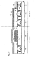
- FIG. 12A is a plan view to show a state in which the process has been advanced to the step of sealing the EL element and FIG. 12B is a cross-sectional view taken on line A - A' in FIG. 12A .
- a section 1200 indicated by a dotted line is a pixel section and a section 1201 is a source signal side driving circuit and a section 1202 is a gate signal side driving circuit and a section 1203 is a sensor section.
- a reference numeral 1204 designates a covering member and 1205 designates a first sealing member and 1206 designates a second sealing member.
- a reference numeral 1207 designates a TAB tape to be an external input terminal that receives a video signal or a clock signal from an external driving circuit and a correction circuit.
- the TAB tape may be provided with a printed wiring board (PWB) or be a TCP.
- the pixel section 1200 includes a plurality of pixels each of which includes a current control TFT 456 and a pixel electrode 423 electrically connected to the drain of the current control TFT 456.
- the source signal side driving circuit 1201 includes a CMOS circuit made of a combination of an n-channel type TFT 453 and a p-channel type TFT 454.
- the sensor section 1203 includes a photodiode 452 connected to a reset TFT 451.
- a polarizing plate typically, a circular polarizing plate
- the pixel electrode 423 functions as the anode of the EL element. Also, banks 424 are formed on both ends of the pixel electrode 423, and an EL layer 425 and the cathode 426 of the EL element are formed on the pixel electrode 423.
- the cathode 426 functions also as a wiring common to all the pixels and finally is electrically connected to a TAB tape 1207. Further, all the elements included in the pixel section 1200, the source signal side driving circuit 1201, and the sensor section 1203 are covered with a protective film 427.
- the covering member 1204 is placed to the insulating body 400 with the first sealing member 1205.
- a spacer may be provided so as to ensure a gap between the covering member 1204 and the EL element.
- a space 1208 is formed inside the first sealing member 1205.
- the first sealing member 1205 is made of a material which does not allow moisture or oxygen to pass through. Further, it is effective that a substance having effects of absorbing moisture or preventing oxidation is disposed in the space 1208.
- carbon films specifically, a diamond like carbon film
- 1209a, 1209b having a thickness of from 2 nm to 30 nm be formed as protective films on the obverse surface and the reverse surface of the covering member 1204.
- Such a carbon film prevents the entry of oxygen and water and mechanically protects the surface of the covering member 1204.
- a second sealing member 1206 is formed such that it covers the exposed surface of the first sealing member 1205.
- the second sealing member 1206 can be formed of the same material as the first sealing member 1205.
- the EL element By sealing the EL element by the structure described above, the EL element can be completely shielded from the outside to prevent a substance for degrading the EL layer by oxidation such as moisture and oxygen from entering from the outside. Accordingly, this can provide a light emitting device having high reliability.
- a light emitting module with a pixel section, a driving circuit, and a sensor section which are formed on the same insulating body, and further provided with a TAB tape is referred to as a light emitting module of a built-in driving circuit type in the present specification.
- the light emitting module of a built-in driving circuit type shown in FIGS. 12A and 12B is an example in which a pixel section and a driving circuit are integrally formed on the same insulating body, but the driving circuit may be provided as an external IC (integrated circuit). In this case, the structure will be shown in FIG. 13A .
- a TAB tape 14 is attached to a substrate (active matrix substrate) 10 (including a pixel section 11, wirings 12a, 12b and a sensor section 13) on which a pixel section including a TFT and an EL element is formed and a printed wiring board 15 is connected thereto through the TAB tape 14.
- a substrate active matrix substrate
- 10 including a pixel section 11, wirings 12a, 12b and a sensor section 13
- a printed wiring board 15 is connected thereto through the TAB tape 14.
- FIG. 13B the circuit block diagram of the printed wiring board 15 is shown in FIG. 13B .
- I/O ports also referred to as an input/output section
- a source signal side driving circuit 17 a gate signal side driving circuit 18 and an IC which functions as a correction circuit 20 are mounted in the printed wiring board 15.
- a module with a configuration in which a substrate with a pixel section and a sensor section which are formed on the same insulating body is provided with a TAB tape and a printed wiring board which functions as a driving circuit is provided via the TAB tape, is referred to as a light emitting module of an external driving circuit type in the present specification.
- a light emitting module of a built-in driving circuit type 30 (including a pixel section 31, a source signal side driving circuit 32, a gate signal side driving circuit 33, wirings 32a, 33a, a sensor section 34, and a TAB tape 35) is provided with a printed wiring board 36 via the TAB tape 35.
- a circuit block diagram of the printed wiring board 36 is shown in FIG. 14B .
- the memory section 39 functions as the correction memory shown in FIG. 2 or FIG. 3 and luminance is adjusted by the correction circuit included in the control section 38.
- the control section 38 can control various kinds of signals such as a signal transmitted to the driving circuit or a timing signal.
- a module with the configuration in which a light emitting module of a built-in driving circuit type with a pixel section, a driving circuit and a sensor section which are formed on the same insulating body is provided with a printed wiring board which functions as a controller, is referred to as a light emitting module of an external controller type.
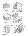
- a light emitting module formed by the use of the present invention is applied to various kinds of electric appliances and a pixel section is used as an image display section.
- the electric appliances in accordance with the present invention include a video camera, a digital camera, a goggle type display (head-mounted display), a navigation system, an audio unit, a note-type personal computer, a game device, a portable device (a mobile computer, a portable telephone, a portable game device or an electronic book), and an image reproducing device provided with a recording medium.
- FIGS. 15A to 16B The specific examples of these electric appliances will be shown in FIGS. 15A to 16B .
- FIG. 15A is an EL display and includes a box 2001, a support 2002, and a display section 2003.
- a light emitting module in accordance with the present invention can be used as the display section 2003. By applying the light emitting module in accordance with the present invention to the display section, it is possible to improve the visibility of the EL display and to reduce power consumption.
- FIG. 15B is a video camera and includes a main body 2101, a display section 2102, a voice input section 2103, an operating switch 2104, a battery 2105, and an image receiving section 2106.
- the light emitting module in accordance with the present invention can be used as the display section 2102.
- FIG. 15C is a digital camera and includes a main body 2201, a display section 2202, an eyepiece section 2203, and an operating switch 2204.
- the light emitting module in accordance with the present invention can be used as the display section 2202.
- FIG. 15D is an image reproducing device provided with a recording medium (specifically, a DVD reproducing device) and includes a main body 2301, a recording medium (a CD, an LD, or a DVD) 2302, an operating switch 2303, a display section (a) 2304 and a display section (b) 2305.
- the display section (a) 2304 mainly displays image information
- the display section (b) 2305 mainly displays textual information and a light emitting module in accordance with the present invention can be used as the display sections (a), (b).
- the image reproducing device provided with the recording medium includes a CD reproduction device, a game device and the like.
- FIG. 15E is a portable (mobile) computer and includes a main body 2401, a display section 2402, a image receiving section 2403, an operating switch 2404, and a memory slot 2405.
- the light emitting module in accordance with the present invention can be used as the display section 2402.
- This portable computer can record information on a recording medium in which flash memories and non-volatile memories are integrated and can reproduce the information.
- FIG. 15F is a personal computer and includes a main body 2501, a box 2502, a display section 2503, and a keyboard 2504.
- the light emitting module in accordance with the present invention can be used as the display section 2503.
- the light emitting section consumes electric power in the light emitting module, it is preferable that information be displayed such that the light emitting section is made as small as possible. Accordingly, in the case a light emitting module is used as a display section mainly displaying textual information such as a portable information terminal, in particular, a portable telephone, an audio unit, or the like, it is preferable that the light emitting module be driven in such a way that textual information is formed of the light emitting section against the background of non-light emitting section.
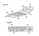
- FIG. 16A shows a portable telephone and has a key operating section (operation section) 2601 and an information displaying section (information display section) 2602 which is connected to the operation section 2601 with a connection section 2603. Also, the operation section 2601 is provided with a voice input section 2604 and an operating key 2605 and the information display section 2602 is provided with a voice output section 2606 and a display section 2607.
- the light emitting module in accordance with the present invention can be used as the display section 2607.
- displaying white letters against a black background can reduce power consumption of the portable telephone.
- the portable telephone shown in FIG. 16A it is also possible to use the portable telephone as a certification system terminal for certifying a user by reading his fingerprint or palm by building a sensor made of a CMOS circuit (CMOS sensor) in the light emitting module used as the display section 2604. Further, it is possible to read the brightness (illuminance) of the outside and to emit light such that information is displayed in a set contrast.
- CMOS sensor CMOS circuit
- the power consumption of the portable telephone by decreasing the luminance of the display section 2604 while the operating switch 2605 is being used and increasing the luminance after the use of the operating switch is finished. Still further, it is possible to reduce the power consumption of the portable telephone by increasing the luminance of the display section 2604 when a signal is received and decreasing the luminance during a telephone conversation. Still further, it is possible to reduce the power consumption of the portable telephone by providing it with a function of turning off the display by a time control unless reset while it is continuously used. Here, these functions may be manually controlled.
- FIG. 16B shows an audio unit mounted in a motor vehicle and includes a box 2701, a display section 2702, and operating switches 2703, 2704.
- the light emitting module in accordance with the present invention can be used as the display section 2702. While an audio unit (car audio unit) mounted in a motor vehicle is shown as an example of the audio unit in the present embodiment, the light emitting module in accordance with the present invention can be applied to an audio unit mounted in the house (audio component).
- the light emitting module is used as the display section 2704, it is possible to reduce power consumption by displaying white letters against a black background.
- the present invention has a wide range of application and can be applied to various kinds of electric appliances. As a result, it is possible to improve the visibility of the display section of the electric appliance and to reduce the power consumption by using a light emitting module which is excellent in visibility in the bright environment and the dark environment and further can reduce power consumption to a minimum in the dark environment. Further, the light emitting module may be applied to the electric appliances of the present embodiment.
- environmental illuminance is sensed by a sensor section provided in a light emitting device, and the correct luminance of an EL element and a correction signal necessary for obtaining the correct luminance are calculated by a correction circuit based on the output signal of the sensor section. Then, the amount of current flowing through the EL element is corrected based on the correction signal to keep the ratio of the luminance of the EL element to the environmental illuminance at a constant value.
- an electric appliance employing the light emitting module in accordance with the present invention can have excellent visibility in a display section and reduce power consumption.
Landscapes
- Engineering & Computer Science (AREA)
- General Physics & Mathematics (AREA)
- Physics & Mathematics (AREA)
- Microelectronics & Electronic Packaging (AREA)
- Computer Hardware Design (AREA)
- Spectroscopy & Molecular Physics (AREA)
- Theoretical Computer Science (AREA)
- Condensed Matter Physics & Semiconductors (AREA)
- Power Engineering (AREA)
- Life Sciences & Earth Sciences (AREA)
- Sustainable Development (AREA)
- Electroluminescent Light Sources (AREA)
- Control Of El Displays (AREA)
- Devices For Indicating Variable Information By Combining Individual Elements (AREA)
- Control Of Indicators Other Than Cathode Ray Tubes (AREA)
Applications Claiming Priority (2)
| Application Number | Priority Date | Filing Date | Title |
|---|---|---|---|
| JP2000176168 | 2000-06-12 | ||
| JP2000176168 | 2000-06-12 |
Publications (3)
| Publication Number | Publication Date |
|---|---|
| EP1164641A2 EP1164641A2 (en) | 2001-12-19 |
| EP1164641A3 EP1164641A3 (en) | 2007-03-28 |
| EP1164641B1 true EP1164641B1 (en) | 2010-02-24 |
Family
ID=18677922
Family Applications (1)
| Application Number | Title | Priority Date | Filing Date |
|---|---|---|---|
| EP01114266A Expired - Lifetime EP1164641B1 (en) | 2000-06-12 | 2001-06-12 | Light emitting module and method of driving the same, and optical sensor |
Country Status (7)
| Country | Link |
|---|---|
| US (2) | US7068246B2 (enExample) |
| EP (1) | EP1164641B1 (enExample) |
| JP (2) | JP2002072963A (enExample) |
| KR (2) | KR100846610B1 (enExample) |
| CN (2) | CN1251333C (enExample) |
| DE (1) | DE60141371D1 (enExample) |
| TW (1) | TW497274B (enExample) |
Families Citing this family (121)
| Publication number | Priority date | Publication date | Assignee | Title |
|---|---|---|---|---|
| TWI252592B (en) | 2000-01-17 | 2006-04-01 | Semiconductor Energy Lab | EL display device |
| US6995753B2 (en) * | 2000-06-06 | 2006-02-07 | Semiconductor Energy Laboratory Co., Ltd. | Display device and method of manufacturing the same |
| JP2002072963A (ja) * | 2000-06-12 | 2002-03-12 | Semiconductor Energy Lab Co Ltd | 発光モジュールおよびその駆動方法並びに光センサ |
| JP4703883B2 (ja) | 2001-04-09 | 2011-06-15 | 株式会社半導体エネルギー研究所 | 半導体装置の作製方法 |
| US7351605B2 (en) | 2001-04-09 | 2008-04-01 | Semiconductor Energy Laboratory Co., Ltd. | Method of manufacturing a semiconductor device |
| US20030191693A1 (en) | 2002-04-08 | 2003-10-09 | Itamar Aphek | System and method for conducting an advertising business |
| JP2003045874A (ja) | 2001-07-27 | 2003-02-14 | Semiconductor Energy Lab Co Ltd | 金属配線およびその作製方法、並びに金属配線基板およびその作製方法 |
| CN1643564A (zh) * | 2002-03-27 | 2005-07-20 | 三洋电机株式会社 | 显示装置、便携式终端及便携式终端中的亮度控制方法 |
| JP2003302938A (ja) * | 2002-04-10 | 2003-10-24 | Tohoku Pioneer Corp | 発光表示パネルの駆動装置 |
| TWI269248B (en) | 2002-05-13 | 2006-12-21 | Semiconductor Energy Lab | Display device |
| EP1376697A1 (en) | 2002-06-17 | 2004-01-02 | CSEM Centre Suisse d'Electronique et de Microtechnique SA | Integrated-optical microsystem based on organic semiconductors |
| JP4227770B2 (ja) * | 2002-07-10 | 2009-02-18 | シャープ株式会社 | 表示装置およびそれを備えた画像読み取り/表示システム |
| KR100480174B1 (ko) * | 2002-08-23 | 2005-04-06 | 엘지전자 주식회사 | 플라즈마 디스플레이 패널의 구동장치 및 그의 제조 방법 |
| JP2004145278A (ja) * | 2002-08-30 | 2004-05-20 | Seiko Epson Corp | 電子回路、電子回路の駆動方法、電気光学装置、電気光学装置の駆動方法及び電子機器 |
| AU2003301712A1 (en) * | 2002-10-31 | 2004-05-25 | Semiconductor Energy Laboratory Co., Ltd. | Display device and controlling method thereof |
| US7265383B2 (en) * | 2002-12-13 | 2007-09-04 | Semiconductor Energy Laboratory Co., Ltd. | Light emitting device |
| KR100565591B1 (ko) * | 2003-01-17 | 2006-03-30 | 엘지전자 주식회사 | 자체 발광 소자의 구동방법 |
| EP1610287B1 (en) | 2003-03-20 | 2012-02-22 | Ryotaro Ojima | Advertisement information providing system using transparent organic el display, advertisement information providing method using the system |
| JP2005070740A (ja) * | 2003-03-20 | 2005-03-17 | Ryotaro Oshima | 透明な有機elディスプレイを用いた広告情報提供システム及びこれを用いた広告情報提供方法及び記録媒体。 |
| WO2004090487A1 (ja) * | 2003-03-26 | 2004-10-21 | Semiconductor Energy Laboratory Co., Ltd. | 多方向からの光を検出する光センサ、携帯通信機器及び表示方法 |
| TW572302U (en) * | 2003-04-08 | 2004-01-11 | Richtek Technology Corp | Energy-saving type auto-contrast compensation device of OLED |
| US7026597B2 (en) * | 2003-04-09 | 2006-04-11 | Eastman Kodak Company | OLED display with integrated elongated photosensor |
| JP4152797B2 (ja) | 2003-04-14 | 2008-09-17 | 株式会社半導体エネルギー研究所 | アクティブマトリクス型表示装置 |
| JP2004354684A (ja) * | 2003-05-29 | 2004-12-16 | Tohoku Pioneer Corp | 自発光型表示装置 |
| US7557779B2 (en) * | 2003-06-13 | 2009-07-07 | Semiconductor Energy Laboratory Co., Ltd. | Display device |
| JP2005017438A (ja) * | 2003-06-24 | 2005-01-20 | Tohoku Pioneer Corp | 発光表示パネルの駆動装置および駆動方法 |
| JP2005017566A (ja) * | 2003-06-25 | 2005-01-20 | Sanyo Electric Co Ltd | 表示装置およびその制御方法 |
| JP2005043672A (ja) | 2003-07-22 | 2005-02-17 | Toshiba Matsushita Display Technology Co Ltd | アレイ基板およびその製造方法 |
| US6870323B1 (en) * | 2003-10-02 | 2005-03-22 | Eastman Kodak Company | Color display with white light emitting elements |
| EP1523043B1 (en) * | 2003-10-06 | 2011-12-28 | Semiconductor Energy Laboratory Co., Ltd. | Optical sensor and method for manufacturing the same |
| KR100957585B1 (ko) * | 2003-10-15 | 2010-05-13 | 삼성전자주식회사 | 광 감지부를 갖는 전자 디스플레이 장치 |
| US20070171157A1 (en) * | 2003-10-15 | 2007-07-26 | Samsung Electronics Co., Ltd | Display apparatus having photo sensor |
| US7038259B2 (en) * | 2003-10-22 | 2006-05-02 | Micron Technology, Inc. | Dual capacitor structure for imagers and method of formation |
| US20050104821A1 (en) * | 2003-11-14 | 2005-05-19 | Nokia Corporation | Display arrangement |
| CN100419534C (zh) * | 2003-12-08 | 2008-09-17 | 索尼株式会社 | 液晶显示设备和背光调节方法 |
| US7358530B2 (en) * | 2003-12-12 | 2008-04-15 | Palo Alto Research Center Incorporated | Thin-film transistor array with ring geometry |
| KR100833951B1 (ko) * | 2003-12-13 | 2008-05-30 | 삼성전자주식회사 | 디스플레이장치 및 그 제어방법 |
| KR100591548B1 (ko) * | 2003-12-30 | 2006-06-19 | 엘지.필립스 엘시디 주식회사 | 유기전계 발광소자 |
| US20050175043A1 (en) * | 2004-01-29 | 2005-08-11 | Seiko Epson Corporation | Optical head |
| GB0406107D0 (en) * | 2004-03-17 | 2004-04-21 | Koninkl Philips Electronics Nv | Electroluminescent display devices |
| JP2005308857A (ja) | 2004-04-19 | 2005-11-04 | Sony Corp | アクティブマトリクス型表示装置およびその駆動方法 |
| JP2006030318A (ja) * | 2004-07-12 | 2006-02-02 | Sanyo Electric Co Ltd | 表示装置 |
| KR100669720B1 (ko) * | 2004-08-06 | 2007-01-16 | 삼성에스디아이 주식회사 | 평판 디스플레이 장치 |
| JP4744828B2 (ja) * | 2004-08-26 | 2011-08-10 | 浜松ホトニクス株式会社 | 光検出装置 |
| JP4667079B2 (ja) * | 2005-03-07 | 2011-04-06 | シャープ株式会社 | 表示装置 |
| US20090122039A1 (en) * | 2005-04-28 | 2009-05-14 | Hiromi Katoh | Display apparatus and electronic device provided with the same |
| TWI304199B (en) * | 2005-08-02 | 2008-12-11 | Chi Mei El Corp | Flat panel display, display driving apparatus thereof and shift register thereof |
| US7986287B2 (en) * | 2005-08-26 | 2011-07-26 | Semiconductor Energy Laboratory Co., Ltd. | Display device and method of driving the same |
| KR100821070B1 (ko) * | 2006-11-07 | 2008-04-08 | 삼성에스디아이 주식회사 | 포토 다이오드 및 이를 이용한 유기 전계 발광표시장치 |
| US8477125B2 (en) * | 2005-12-21 | 2013-07-02 | Samsung Display Co., Ltd. | Photo sensor and organic light-emitting display using the same |
| EP1804229B1 (en) * | 2005-12-28 | 2016-08-17 | Semiconductor Energy Laboratory Co., Ltd. | Display device and method for inspecting the same |
| KR101367139B1 (ko) * | 2006-02-06 | 2014-02-26 | 삼성디스플레이 주식회사 | 표시 장치와 그 제조방법 |
| EP1816681A3 (en) * | 2006-02-06 | 2012-05-30 | Samsung Electronics Co., Ltd. | Display device and manufacturing method of the same |
| KR100746783B1 (ko) * | 2006-02-28 | 2007-08-06 | 엘지전자 주식회사 | 발광소자 패키지 및 그 제조방법 |
| CN2922026Y (zh) * | 2006-04-29 | 2007-07-11 | 亿光电子工业股份有限公司 | 发光二极管显示器 |
| EP1863105B1 (en) * | 2006-06-02 | 2020-02-19 | Semiconductor Energy Laboratory Co., Ltd. | Light-emitting element, light-emitting device, and electronic device |
| FR2903224A1 (fr) * | 2006-06-30 | 2008-01-04 | Thomson Licensing Sa | Dispositif d'affichage et utilisations de celui-ci. |
| KR100769432B1 (ko) * | 2006-07-04 | 2007-10-22 | 삼성에스디아이 주식회사 | 유기전계발광 소자 및 그의 제조 방법 |
| TW200804900A (en) * | 2006-07-07 | 2008-01-16 | Innolux Display Corp | Liquid crystal display device |
| KR100796657B1 (ko) * | 2006-08-10 | 2008-01-22 | 삼성에스디아이 주식회사 | 풀 컬러 유기 발광 표시장치 및 이의 구동 방법 |
| TWI442368B (zh) * | 2006-10-26 | 2014-06-21 | Semiconductor Energy Lab | 電子裝置,顯示裝置,和半導體裝置,以及其驅動方法 |
| KR101315375B1 (ko) * | 2006-11-08 | 2013-10-08 | 삼성디스플레이 주식회사 | 표시 장치 |
| JP2008122659A (ja) * | 2006-11-13 | 2008-05-29 | Seiko Epson Corp | 液晶表示装置及び液晶表示装置の製造方法並びに電子機器 |
| KR100848337B1 (ko) * | 2006-12-19 | 2008-07-25 | 삼성에스디아이 주식회사 | 평판 표시 장치 |
| JP2008158285A (ja) * | 2006-12-25 | 2008-07-10 | Canon Inc | 画像表示装置 |
| JP5259132B2 (ja) * | 2006-12-27 | 2013-08-07 | 三星ディスプレイ株式會社 | 周辺光感知回路及びこれを有する平板表示装置 |
| JP4959449B2 (ja) | 2006-12-27 | 2012-06-20 | 三星モバイルディスプレイ株式會社 | 周辺光感知回路及びこれを有する平板表示装置 |
| DE102007001742A1 (de) * | 2007-01-11 | 2008-07-17 | Osram Opto Semiconductors Gmbh | Optoelektronische Vorrichtung und Verfahren zur Herstellung einer optoelektronischen Vorrichtung |
| US8207589B2 (en) * | 2007-02-15 | 2012-06-26 | Semiconductor Energy Laboratory Co., Ltd. | Photoelectric conversion device and electronic device, and method for manufacturing photoelectric conversion device |
| KR100837779B1 (ko) * | 2007-02-21 | 2008-06-13 | 리디스 테크놀로지 인코포레이티드 | 디스플레이 표시장치 및 그의 구동방법 |
| TWI361019B (en) * | 2007-05-22 | 2012-03-21 | Chimei Innolux Corp | System for displaying images including active-matr |
| JP4925929B2 (ja) * | 2007-06-07 | 2012-05-09 | 株式会社 日立ディスプレイズ | 表示装置 |
| KR100840098B1 (ko) | 2007-07-04 | 2008-06-19 | 삼성에스디아이 주식회사 | 유기전계발광 소자 및 그의 제조 방법 |
| KR100840099B1 (ko) | 2007-07-04 | 2008-06-19 | 삼성에스디아이 주식회사 | 포토 다이어드를 구비한 유기전계발광 소자의 제조 방법 |
| US20090020838A1 (en) | 2007-07-17 | 2009-01-22 | Taiwan Semiconductor Manufacturing Company, Ltd. | Apparatus and method for reducing optical cross-talk in image sensors |
| DE102007034782A1 (de) * | 2007-07-25 | 2009-01-29 | Atmel Germany Gmbh | Halbleiterbauelement, Beleuchtungseinrichtung für Matrixbildschirme und Verfahren zum Herstellen eines Halbleiterbauelements |
| TWI353063B (en) * | 2007-07-27 | 2011-11-21 | Au Optronics Corp | Photo detector and method for fabricating the same |
| KR100882693B1 (ko) * | 2007-09-14 | 2009-02-06 | 삼성모바일디스플레이주식회사 | 발광표시장치 및 그의 제조방법 |
| US7960682B2 (en) | 2007-12-13 | 2011-06-14 | Apple Inc. | Display device control based on integrated ambient light detection and lighting source characteristics |
| JP2011509530A (ja) * | 2008-01-08 | 2011-03-24 | モクストロニクス,インコーポレイテッド | 高性能ヘテロ構造発光素子および方法 |
| US9570004B1 (en) * | 2008-03-16 | 2017-02-14 | Nongqiang Fan | Method of driving pixel element in active matrix display |
| EP2151811A3 (en) | 2008-08-08 | 2010-07-21 | Semiconductor Energy Laboratory Co, Ltd. | Display device and electronic device |
| JP5451036B2 (ja) * | 2008-11-21 | 2014-03-26 | 株式会社ジャパンディスプレイ | 表示装置及びその製造方法 |
| KR101002663B1 (ko) * | 2008-12-11 | 2010-12-21 | 삼성모바일디스플레이주식회사 | 유기 발광 표시 장치 |
| KR101002659B1 (ko) * | 2008-12-23 | 2010-12-20 | 삼성모바일디스플레이주식회사 | 유기 발광 표시 장치 |
| KR101015851B1 (ko) * | 2009-02-09 | 2011-02-23 | 삼성모바일디스플레이주식회사 | 유기 발광 표시 장치 |
| KR101022651B1 (ko) * | 2009-02-11 | 2011-03-22 | 삼성모바일디스플레이주식회사 | 광센서, 광센서를 포함하는 광센서 장치, 및 이를 포함하는디스플레이 장치 |
| JP4516625B1 (ja) * | 2009-08-11 | 2010-08-04 | 正幸 安部 | 電子装置 |
| KR101074815B1 (ko) * | 2010-03-16 | 2011-10-19 | 삼성모바일디스플레이주식회사 | 평판 디스플레이 장치 |
| KR20140054465A (ko) | 2010-09-15 | 2014-05-08 | 가부시키가이샤 한도오따이 에네루기 켄큐쇼 | 반도체 장치 및 표시 장치 |
| JP5982147B2 (ja) | 2011-04-01 | 2016-08-31 | 株式会社半導体エネルギー研究所 | 発光装置 |
| US8922464B2 (en) | 2011-05-11 | 2014-12-30 | Semiconductor Energy Laboratory Co., Ltd. | Active matrix display device and driving method thereof |
| US8710505B2 (en) | 2011-08-05 | 2014-04-29 | Semiconductor Energy Laboratory Co., Ltd. | Semiconductor device |
| JP6050054B2 (ja) | 2011-09-09 | 2016-12-21 | 株式会社半導体エネルギー研究所 | 半導体装置 |
| WO2013080261A1 (ja) | 2011-11-30 | 2013-06-06 | パナソニック株式会社 | 表示パネル及び表示パネルの製造方法 |
| JPWO2013080261A1 (ja) * | 2011-11-30 | 2015-04-27 | パナソニック株式会社 | 表示パネル及び表示パネルの製造方法 |
| US10043794B2 (en) | 2012-03-22 | 2018-08-07 | Semiconductor Energy Laboratory Co., Ltd. | Semiconductor device and electronic device |
| DE102013201212A1 (de) * | 2013-01-25 | 2014-07-31 | Osram Opto Semiconductors Gmbh | Verfahren zum Betrieb eines organischen optoelektronischen Bauelements |
| KR102147087B1 (ko) * | 2013-12-13 | 2020-08-24 | 엘지디스플레이 주식회사 | 투명 유기 발광 표시 장치 및 그 제조 방법 |
| TWI550836B (zh) * | 2014-05-06 | 2016-09-21 | 友達光電股份有限公司 | 光偵測器及其製造方法 |
| CN105788511B (zh) * | 2014-12-22 | 2021-05-25 | 昆山国显光电有限公司 | 像素驱动电路及显示装置 |
| CN104681655A (zh) * | 2015-01-12 | 2015-06-03 | 京东方科技集团股份有限公司 | 一种探测基板及其制备方法、探测器 |
| JP2017009725A (ja) * | 2015-06-19 | 2017-01-12 | ソニー株式会社 | 表示装置 |
| CN105206634B (zh) * | 2015-08-25 | 2018-10-16 | 南京剑桥新港科技发展有限公司 | 一种多样化有源像素生物传感探测系统 |
| KR102380922B1 (ko) * | 2015-09-11 | 2022-04-04 | 엘지디스플레이 주식회사 | 유기발광 표시장치 |
| WO2017098758A1 (ja) * | 2015-12-08 | 2017-06-15 | コニカミノルタ株式会社 | 光学式指紋認証装置 |
| KR102536146B1 (ko) * | 2016-04-07 | 2023-05-24 | 삼성전자주식회사 | 디스플레이 장치, 이를 포함하는 전자 장치 및 이의 동작 방법 |
| CN109244089B (zh) * | 2017-07-10 | 2021-08-17 | 京东方科技集团股份有限公司 | 一种感测基板及其制作方法、显示装置 |
| CN109390286B (zh) * | 2017-08-09 | 2022-04-15 | 昆山国显光电有限公司 | 阵列基板及其制造方法、显示面板及其制造方法 |
| KR102017866B1 (ko) * | 2018-01-24 | 2019-09-03 | 연세대학교 산학협력단 | 이미지 센서 내장형 디스플레이 |
| CN108767016B (zh) * | 2018-05-21 | 2021-09-21 | 京东方科技集团股份有限公司 | 一种薄膜晶体管及其制作方法、阵列基板、显示装置 |
| CN109117733B (zh) * | 2018-07-17 | 2020-06-30 | 武汉华星光电半导体显示技术有限公司 | 一种指纹识别oled显示面板及显示装置 |
| CN110071164B (zh) * | 2019-05-07 | 2021-05-04 | 京东方科技集团股份有限公司 | 一种显示基板及其亮度调节方法、显示装置 |
| DE112020002314T5 (de) * | 2019-05-10 | 2022-03-10 | Semiconductor Energy Laboratory Co., Ltd. | Verbundgerät und Betriebsverfahren für elektronisches Gerät |
| WO2021009587A1 (ja) * | 2019-07-12 | 2021-01-21 | 株式会社半導体エネルギー研究所 | 機能パネル、表示装置、入出力装置、情報処理装置 |
| WO2021069999A1 (ja) | 2019-10-11 | 2021-04-15 | 株式会社半導体エネルギー研究所 | 機能パネル、表示装置、入出力装置、情報処理装置 |
| KR102737571B1 (ko) * | 2020-01-22 | 2024-12-03 | 삼성전자주식회사 | 디스플레이를 포함하는 전자 장치 및 전자 장치의 동작 방법 |
| CN111312768A (zh) * | 2020-02-24 | 2020-06-19 | 京东方科技集团股份有限公司 | 显示基板及其制备方法、显示面板 |
| US10957248B1 (en) * | 2020-04-12 | 2021-03-23 | Wuhan China Star Optoelectronics Semiconductor Display Technology Co., Ltd. | Display panel and mobile terminal |
| CN112562577A (zh) * | 2020-11-19 | 2021-03-26 | 江苏玄博智能标识科技有限公司 | 一种标识牌智能控制系统及其控制方法 |
| CN112736117B (zh) * | 2020-12-23 | 2024-04-26 | 深圳市华星光电半导体显示技术有限公司 | 显示面板 |
Family Cites Families (84)
| Publication number | Priority date | Publication date | Assignee | Title |
|---|---|---|---|---|
| US4356429A (en) * | 1980-07-17 | 1982-10-26 | Eastman Kodak Company | Organic electroluminescent cell |
| US4539507A (en) * | 1983-03-25 | 1985-09-03 | Eastman Kodak Company | Organic electroluminescent devices having improved power conversion efficiencies |
| JPS61252589A (ja) * | 1985-05-02 | 1986-11-10 | 日産自動車株式会社 | El表示装置 |
| JPS62125329A (ja) * | 1985-11-27 | 1987-06-06 | Hosiden Electronics Co Ltd | 透過形表示装置 |
| US4885211A (en) * | 1987-02-11 | 1989-12-05 | Eastman Kodak Company | Electroluminescent device with improved cathode |
| US4720432A (en) * | 1987-02-11 | 1988-01-19 | Eastman Kodak Company | Electroluminescent device with organic luminescent medium |
| US4769292A (en) * | 1987-03-02 | 1988-09-06 | Eastman Kodak Company | Electroluminescent device with modified thin film luminescent zone |
| US4950950A (en) * | 1989-05-18 | 1990-08-21 | Eastman Kodak Company | Electroluminescent device with silazane-containing luminescent zone |
| JPH03245181A (ja) * | 1990-02-23 | 1991-10-31 | Sanyo Electric Co Ltd | 発光輝度の自動調整回路 |
| US5059861A (en) * | 1990-07-26 | 1991-10-22 | Eastman Kodak Company | Organic electroluminescent device with stabilizing cathode capping layer |
| US5047687A (en) * | 1990-07-26 | 1991-09-10 | Eastman Kodak Company | Organic electroluminescent device with stabilized cathode |
| US5059862A (en) * | 1990-07-26 | 1991-10-22 | Eastman Kodak Company | Electroluminescent device with improved cathode |
| US5073446A (en) * | 1990-07-26 | 1991-12-17 | Eastman Kodak Company | Organic electroluminescent device with stabilizing fused metal particle cathode |
| US5061617A (en) * | 1990-12-07 | 1991-10-29 | Eastman Kodak Company | Process for the preparation of high chloride tabular grain emulsions |
| JPH04326849A (ja) | 1991-04-26 | 1992-11-16 | Matsushita Electric Ind Co Ltd | イメージセンサ |
| US5151629A (en) * | 1991-08-01 | 1992-09-29 | Eastman Kodak Company | Blue emitting internal junction organic electroluminescent device (I) |
| JPH0588655A (ja) | 1991-09-27 | 1993-04-09 | Toshiba Corp | 画面輝度制御装置 |
| US5294870A (en) * | 1991-12-30 | 1994-03-15 | Eastman Kodak Company | Organic electroluminescent multicolor image display device |
| US5294869A (en) * | 1991-12-30 | 1994-03-15 | Eastman Kodak Company | Organic electroluminescent multicolor image display device |
| JPH05241512A (ja) | 1992-02-28 | 1993-09-21 | Matsushita Electric Works Ltd | 表示装置 |
| US5432015A (en) | 1992-05-08 | 1995-07-11 | Westaim Technologies, Inc. | Electroluminescent laminate with thick film dielectric |
| US5302966A (en) * | 1992-06-02 | 1994-04-12 | David Sarnoff Research Center, Inc. | Active matrix electroluminescent display and method of operation |
| JP3526058B2 (ja) * | 1992-08-19 | 2004-05-10 | セイコーインスツルメンツ株式会社 | 光弁用半導体装置 |
| JP2924506B2 (ja) | 1992-10-27 | 1999-07-26 | 日本電気株式会社 | アクティブマトリックス型液晶表示装置の画素構造 |
| US5285060A (en) * | 1992-12-15 | 1994-02-08 | Donnelly Corporation | Display for automatic rearview mirror |
| JP2752309B2 (ja) * | 1993-01-19 | 1998-05-18 | 松下電器産業株式会社 | 表示装置 |
| JPH06259030A (ja) * | 1993-03-03 | 1994-09-16 | Yazaki Corp | 発光輝度自動調整装置 |
| US5617112A (en) * | 1993-12-28 | 1997-04-01 | Nec Corporation | Display control device for controlling brightness of a display installed in a vehicular cabin |
| JP3366717B2 (ja) * | 1994-01-17 | 2003-01-14 | 小糸工業株式会社 | 情報表示装置 |
| US5510851A (en) * | 1994-03-29 | 1996-04-23 | Radius Inc. | Method and apparatus for dynamic purity correction |
| JPH07325549A (ja) * | 1994-05-31 | 1995-12-12 | Matsushita Electric Ind Co Ltd | 文字表示装置 |
| JP3254335B2 (ja) | 1994-09-08 | 2002-02-04 | 出光興産株式会社 | 有機el素子の封止方法および有機el素子 |
| WO1996008122A1 (fr) * | 1994-09-08 | 1996-03-14 | Idemitsu Kosan Co., Ltd. | Procede d'enrobage d'un element electroluminescent organique et d'un autre element electroluminescent organique |
| EP0717445B1 (en) | 1994-12-14 | 2009-06-24 | Eastman Kodak Company | An electroluminescent device having an organic electroluminescent layer |
| US5644327A (en) | 1995-06-07 | 1997-07-01 | David Sarnoff Research Center, Inc. | Tessellated electroluminescent display having a multilayer ceramic substrate |
| US5760760A (en) * | 1995-07-17 | 1998-06-02 | Dell Usa, L.P. | Intelligent LCD brightness control system |
| US5702323A (en) * | 1995-07-26 | 1997-12-30 | Poulton; Craig K. | Electronic exercise enhancer |
| JPH0981070A (ja) * | 1995-09-18 | 1997-03-28 | Kokusai Electric Co Ltd | Led表示装置 |
| JPH09146073A (ja) | 1995-11-21 | 1997-06-06 | Nec Corp | 液晶表示装置のバックライト調光回路 |
| US5956015A (en) * | 1995-12-18 | 1999-09-21 | Ricoh Company, Ltd. | Method and system for correcting color display based upon ambient light |
| US5831693A (en) * | 1996-02-22 | 1998-11-03 | Honeywell | Integrated light sensor for an active matrix liquid crystal display panel |
| JPH09304730A (ja) | 1996-05-15 | 1997-11-28 | Sony Corp | 光学視覚装置 |
| JP3435288B2 (ja) * | 1996-06-20 | 2003-08-11 | ペンタックス株式会社 | カメラシステム |
| US6271813B1 (en) | 1996-08-30 | 2001-08-07 | Lear Automotive Dearborn, Inc. | Voltage control for adjusting the brightness of a screen display |
| KR100226548B1 (ko) * | 1996-12-24 | 1999-10-15 | 김영환 | 웨이퍼 습식 처리 장치 |
| US5990629A (en) * | 1997-01-28 | 1999-11-23 | Casio Computer Co., Ltd. | Electroluminescent display device and a driving method thereof |
| US6005350A (en) * | 1997-02-24 | 1999-12-21 | Matsushita Electric Industrial Co., Ltd. | Electroluminescent driving apparatus with photodetector |
| JP3887826B2 (ja) * | 1997-03-12 | 2007-02-28 | セイコーエプソン株式会社 | 表示装置及び電子機器 |
| JPH10282924A (ja) * | 1997-04-02 | 1998-10-23 | Rohm Co Ltd | 発光表示装置 |
| EP0915367B1 (en) * | 1997-04-22 | 2007-06-06 | Matsushita Electric Industrial Co., Ltd. | Liquid crystal display with image reading function, image reading method and manufacturing method |
| JPH10319910A (ja) * | 1997-05-15 | 1998-12-04 | Tdk Corp | 有機elディスプレイの駆動装置 |
| TW382687B (en) | 1997-05-24 | 2000-02-21 | Ind Tech Res Inst | Field emission display with automatic brightness adjustment to background |
| US6069598A (en) | 1997-08-29 | 2000-05-30 | Candescent Technologies Corporation | Circuit and method for controlling the brightness of an FED device in response to a light sensor |
| JP4013293B2 (ja) * | 1997-09-01 | 2007-11-28 | セイコーエプソン株式会社 | 表示装置兼用型イメージセンサ装置及びアクティブマトリクス型表示装置 |
| JPH1185059A (ja) * | 1997-09-05 | 1999-03-30 | Casio Comput Co Ltd | 表示素子、表示素子の製造方法及び表示素子の駆動方法 |
| JP4076248B2 (ja) * | 1997-09-09 | 2008-04-16 | オリンパス株式会社 | 色再現装置 |
| JP4183786B2 (ja) * | 1997-10-17 | 2008-11-19 | 株式会社半導体エネルギー研究所 | 半導体装置の作製方法 |
| US6337675B1 (en) * | 1997-10-30 | 2002-01-08 | Ut Automotive Dearborn, Inc | Display system with automatic and manual brightness control |
| US6297791B1 (en) * | 1997-11-21 | 2001-10-02 | Seiko Epson Corporation | Adjustment method of display device |
| JP2994631B2 (ja) | 1997-12-10 | 1999-12-27 | 松下電器産業株式会社 | Pdp表示の駆動パルス制御装置 |
| KR19990049744A (ko) * | 1997-12-15 | 1999-07-05 | 김영환 | Lcd 화면 밝기 자동조정장치 및 방법 |
| JP3960630B2 (ja) | 1998-02-06 | 2007-08-15 | コーニンクレッカ フィリップス エレクトロニクス エヌ ヴィ | 有機電界発光装置 |
| JPH11271714A (ja) * | 1998-03-24 | 1999-10-08 | Toshiba Corp | アレイ基板、液晶表示装置及びその駆動方法 |
| JP2002511608A (ja) * | 1998-04-15 | 2002-04-16 | ケンブリッジ ディスプレイ テクノロジー リミテッド | 電力消費の少ないモードを有するディスプレイ制御デバイス |
| JP3985981B2 (ja) * | 1998-04-16 | 2007-10-03 | 株式会社半導体エネルギー研究所 | 表示装置および表示装置補正システム |
| JPH11326954A (ja) * | 1998-05-15 | 1999-11-26 | Semiconductor Energy Lab Co Ltd | 半導体装置 |
| JP2000012215A (ja) | 1998-06-25 | 2000-01-14 | Shichizun Denshi:Kk | El駆動回路システム |
| JP2000081608A (ja) * | 1998-06-29 | 2000-03-21 | Sanyo Electric Co Ltd | 集光機構付液晶表示装置 |
| US6417825B1 (en) * | 1998-09-29 | 2002-07-09 | Sarnoff Corporation | Analog active matrix emissive display |
| JP3716651B2 (ja) * | 1998-10-20 | 2005-11-16 | カシオ計算機株式会社 | 表示装置 |
| JP2000147458A (ja) * | 1998-11-12 | 2000-05-26 | Matsushita Electric Ind Co Ltd | 液晶表示装置 |
| KR100317281B1 (ko) * | 1998-11-20 | 2002-01-15 | 구자홍 | 자체발광소자의구동방법 |
| JP4566311B2 (ja) | 1998-12-18 | 2010-10-20 | 株式会社半導体エネルギー研究所 | ゴーグル型表示装置 |
| JP3792950B2 (ja) | 1999-07-15 | 2006-07-05 | セイコーインスツル株式会社 | 有機el表示装置、及び、有機el素子の駆動方法 |
| JP2001092412A (ja) * | 1999-09-17 | 2001-04-06 | Pioneer Electronic Corp | アクティブマトリクス型表示装置 |
| US6392617B1 (en) * | 1999-10-27 | 2002-05-21 | Agilent Technologies, Inc. | Active matrix light emitting diode display |
| TW480727B (en) * | 2000-01-11 | 2002-03-21 | Semiconductor Energy Laboratro | Semiconductor display device |
| WO2001069583A1 (en) * | 2000-03-14 | 2001-09-20 | Koninklijke Philips Electronics N.V. | Electroluminescent display device with luminance correction in dependence on age and ambient light |
| US6995753B2 (en) * | 2000-06-06 | 2006-02-07 | Semiconductor Energy Laboratory Co., Ltd. | Display device and method of manufacturing the same |
| JP2002072963A (ja) * | 2000-06-12 | 2002-03-12 | Semiconductor Energy Lab Co Ltd | 発光モジュールおよびその駆動方法並びに光センサ |
| US6528951B2 (en) * | 2000-06-13 | 2003-03-04 | Semiconductor Energy Laboratory Co., Ltd. | Display device |
| US7030551B2 (en) * | 2000-08-10 | 2006-04-18 | Semiconductor Energy Laboratory Co., Ltd. | Area sensor and display apparatus provided with an area sensor |
| US7053874B2 (en) * | 2000-09-08 | 2006-05-30 | Semiconductor Energy Laboratory Co., Ltd. | Light emitting device and driving method thereof |
| US6774578B2 (en) * | 2000-09-19 | 2004-08-10 | Semiconductor Energy Laboratory Co., Ltd. | Self light emitting device and method of driving thereof |
-
2001
- 2001-06-05 JP JP2001169116A patent/JP2002072963A/ja not_active Withdrawn
- 2001-06-06 TW TW090113694A patent/TW497274B/zh not_active IP Right Cessation
- 2001-06-11 CN CNB011214759A patent/CN1251333C/zh not_active Expired - Fee Related
- 2001-06-11 US US09/878,862 patent/US7068246B2/en not_active Expired - Lifetime
- 2001-06-11 CN CN2006100046890A patent/CN1835056B/zh not_active Expired - Fee Related
- 2001-06-12 DE DE60141371T patent/DE60141371D1/de not_active Expired - Lifetime
- 2001-06-12 EP EP01114266A patent/EP1164641B1/en not_active Expired - Lifetime
- 2001-06-12 KR KR1020010032850A patent/KR100846610B1/ko not_active Expired - Fee Related
-
2005
- 2005-12-27 US US11/319,038 patent/US7515125B2/en not_active Expired - Fee Related
-
2006
- 2006-06-12 KR KR1020060052594A patent/KR100810456B1/ko not_active Expired - Fee Related
-
2011
- 2011-10-14 JP JP2011226752A patent/JP5331862B2/ja not_active Expired - Fee Related
Also Published As
| Publication number | Publication date |
|---|---|
| CN1329369A (zh) | 2002-01-02 |
| JP5331862B2 (ja) | 2013-10-30 |
| JP2012058739A (ja) | 2012-03-22 |
| CN1835056B (zh) | 2010-05-26 |
| US7068246B2 (en) | 2006-06-27 |
| US7515125B2 (en) | 2009-04-07 |
| CN1251333C (zh) | 2006-04-12 |
| EP1164641A3 (en) | 2007-03-28 |
| CN1835056A (zh) | 2006-09-20 |
| KR100810456B1 (ko) | 2008-03-07 |
| US20020027229A1 (en) | 2002-03-07 |
| TW497274B (en) | 2002-08-01 |
| KR20060088082A (ko) | 2006-08-03 |
| KR20010112630A (ko) | 2001-12-20 |
| US20060132401A1 (en) | 2006-06-22 |
| KR100846610B1 (ko) | 2008-07-16 |
| EP1164641A2 (en) | 2001-12-19 |
| DE60141371D1 (de) | 2010-04-08 |
| JP2002072963A (ja) | 2002-03-12 |
Similar Documents
| Publication | Publication Date | Title |
|---|---|---|
| EP1164641B1 (en) | Light emitting module and method of driving the same, and optical sensor | |
| US20210295773A1 (en) | Light-emitting device | |
| KR100686479B1 (ko) | El 디스플레이 장치 | |
| US7321672B2 (en) | Image reading apparatus and image reading system equipped with the image reading apparatus | |
| KR100754970B1 (ko) | 표시 시스템 및 액티브 매트릭스형 표시장치 | |
| JP2003295793A (ja) | 発光装置及び電子機器 | |
| JP2006091462A (ja) | 表示装置 | |
| JP2009229908A (ja) | 表示装置 | |
| CN114783345B (zh) | 像素驱动电路、显示模组及显示装置、智能手表 | |
| JP4849821B2 (ja) | 表示装置、電子機器 | |
| JP5312435B2 (ja) | 表示装置 | |
| JP4490403B2 (ja) | 発光装置 |
Legal Events
| Date | Code | Title | Description |
|---|---|---|---|
| PUAI | Public reference made under article 153(3) epc to a published international application that has entered the european phase |
Free format text: ORIGINAL CODE: 0009012 |
|
| AK | Designated contracting states |
Kind code of ref document: A2 Designated state(s): AT BE CH CY DE DK ES FI FR GB GR IE IT LI LU MC NL PT SE TR |
|
| AX | Request for extension of the european patent |
Free format text: AL;LT;LV;MK;RO;SI |
|
| PUAL | Search report despatched |
Free format text: ORIGINAL CODE: 0009013 |
|
| AK | Designated contracting states |
Kind code of ref document: A3 Designated state(s): AT BE CH CY DE DK ES FI FR GB GR IE IT LI LU MC NL PT SE TR |
|
| AX | Request for extension of the european patent |
Extension state: AL LT LV MK RO SI |
|
| 17P | Request for examination filed |
Effective date: 20070925 |
|
| AKX | Designation fees paid |
Designated state(s): DE FI FR GB NL |
|
| 17Q | First examination report despatched |
Effective date: 20080207 |
|
| GRAP | Despatch of communication of intention to grant a patent |
Free format text: ORIGINAL CODE: EPIDOSNIGR1 |
|
| RIC1 | Information provided on ipc code assigned before grant |
Ipc: H01L 27/00 20060101ALI20090527BHEP Ipc: H01L 33/00 20060101ALI20090527BHEP Ipc: G01J 1/44 20060101ALN20090527BHEP Ipc: H01L 27/15 20060101AFI20090527BHEP Ipc: G09G 3/32 20060101ALN20090527BHEP |
|
| GRAS | Grant fee paid |
Free format text: ORIGINAL CODE: EPIDOSNIGR3 |
|
| GRAA | (expected) grant |
Free format text: ORIGINAL CODE: 0009210 |
|
| AK | Designated contracting states |
Kind code of ref document: B1 Designated state(s): DE FI FR GB NL |
|
| REG | Reference to a national code |
Ref country code: GB Ref legal event code: FG4D |
|
| REG | Reference to a national code |
Ref country code: NL Ref legal event code: T3 |
|
| REF | Corresponds to: |
Ref document number: 60141371 Country of ref document: DE Date of ref document: 20100408 Kind code of ref document: P |
|
| PLBE | No opposition filed within time limit |
Free format text: ORIGINAL CODE: 0009261 |
|
| STAA | Information on the status of an ep patent application or granted ep patent |
Free format text: STATUS: NO OPPOSITION FILED WITHIN TIME LIMIT |
|
| 26N | No opposition filed |
Effective date: 20101125 |
|
| PGFP | Annual fee paid to national office [announced via postgrant information from national office to epo] |
Ref country code: NL Payment date: 20120614 Year of fee payment: 12 |
|
| PGFP | Annual fee paid to national office [announced via postgrant information from national office to epo] |
Ref country code: GB Payment date: 20120606 Year of fee payment: 12 Ref country code: FR Payment date: 20120619 Year of fee payment: 12 Ref country code: FI Payment date: 20120612 Year of fee payment: 12 |
|
| REG | Reference to a national code |
Ref country code: NL Ref legal event code: V1 Effective date: 20140101 |
|
| GBPC | Gb: european patent ceased through non-payment of renewal fee |
Effective date: 20130612 |
|
| PG25 | Lapsed in a contracting state [announced via postgrant information from national office to epo] |
Ref country code: FI Free format text: LAPSE BECAUSE OF NON-PAYMENT OF DUE FEES Effective date: 20130612 |
|
| REG | Reference to a national code |
Ref country code: FR Ref legal event code: ST Effective date: 20140228 |
|
| PG25 | Lapsed in a contracting state [announced via postgrant information from national office to epo] |
Ref country code: GB Free format text: LAPSE BECAUSE OF NON-PAYMENT OF DUE FEES Effective date: 20130612 Ref country code: NL Free format text: LAPSE BECAUSE OF NON-PAYMENT OF DUE FEES Effective date: 20140101 |
|
| PG25 | Lapsed in a contracting state [announced via postgrant information from national office to epo] |
Ref country code: FR Free format text: LAPSE BECAUSE OF NON-PAYMENT OF DUE FEES Effective date: 20130701 |
|
| PGFP | Annual fee paid to national office [announced via postgrant information from national office to epo] |
Ref country code: DE Payment date: 20170606 Year of fee payment: 17 |
|
| REG | Reference to a national code |
Ref country code: DE Ref legal event code: R119 Ref document number: 60141371 Country of ref document: DE |
|
| PG25 | Lapsed in a contracting state [announced via postgrant information from national office to epo] |
Ref country code: DE Free format text: LAPSE BECAUSE OF NON-PAYMENT OF DUE FEES Effective date: 20190101 |