EP1022714A2 - Verfahren zur Ansteuerung einer Plasmaanzeigetafel - Google Patents
Verfahren zur Ansteuerung einer Plasmaanzeigetafel Download PDFInfo
- Publication number
- EP1022714A2 EP1022714A2 EP00100160A EP00100160A EP1022714A2 EP 1022714 A2 EP1022714 A2 EP 1022714A2 EP 00100160 A EP00100160 A EP 00100160A EP 00100160 A EP00100160 A EP 00100160A EP 1022714 A2 EP1022714 A2 EP 1022714A2
- Authority
- EP
- European Patent Office
- Prior art keywords
- light
- emission
- pixel data
- driving
- drive
- Prior art date
- Legal status (The legal status is an assumption and is not a legal conclusion. Google has not performed a legal analysis and makes no representation as to the accuracy of the status listed.)
- Withdrawn
Links
Images


Classifications
-
- G—PHYSICS
- G09—EDUCATION; CRYPTOGRAPHY; DISPLAY; ADVERTISING; SEALS
- G09G—ARRANGEMENTS OR CIRCUITS FOR CONTROL OF INDICATING DEVICES USING STATIC MEANS TO PRESENT VARIABLE INFORMATION
- G09G3/00—Control arrangements or circuits, of interest only in connection with visual indicators other than cathode-ray tubes
- G09G3/20—Control arrangements or circuits, of interest only in connection with visual indicators other than cathode-ray tubes for presentation of an assembly of a number of characters, e.g. a page, by composing the assembly by combination of individual elements arranged in a matrix no fixed position being assigned to or needed to be assigned to the individual characters or partial characters
- G09G3/22—Control arrangements or circuits, of interest only in connection with visual indicators other than cathode-ray tubes for presentation of an assembly of a number of characters, e.g. a page, by composing the assembly by combination of individual elements arranged in a matrix no fixed position being assigned to or needed to be assigned to the individual characters or partial characters using controlled light sources
- G09G3/28—Control arrangements or circuits, of interest only in connection with visual indicators other than cathode-ray tubes for presentation of an assembly of a number of characters, e.g. a page, by composing the assembly by combination of individual elements arranged in a matrix no fixed position being assigned to or needed to be assigned to the individual characters or partial characters using controlled light sources using luminous gas-discharge panels, e.g. plasma panels
- G09G3/288—Control arrangements or circuits, of interest only in connection with visual indicators other than cathode-ray tubes for presentation of an assembly of a number of characters, e.g. a page, by composing the assembly by combination of individual elements arranged in a matrix no fixed position being assigned to or needed to be assigned to the individual characters or partial characters using controlled light sources using luminous gas-discharge panels, e.g. plasma panels using AC panels
- G09G3/291—Control arrangements or circuits, of interest only in connection with visual indicators other than cathode-ray tubes for presentation of an assembly of a number of characters, e.g. a page, by composing the assembly by combination of individual elements arranged in a matrix no fixed position being assigned to or needed to be assigned to the individual characters or partial characters using controlled light sources using luminous gas-discharge panels, e.g. plasma panels using AC panels controlling the gas discharge to control a cell condition, e.g. by means of specific pulse shapes
- G09G3/293—Control arrangements or circuits, of interest only in connection with visual indicators other than cathode-ray tubes for presentation of an assembly of a number of characters, e.g. a page, by composing the assembly by combination of individual elements arranged in a matrix no fixed position being assigned to or needed to be assigned to the individual characters or partial characters using controlled light sources using luminous gas-discharge panels, e.g. plasma panels using AC panels controlling the gas discharge to control a cell condition, e.g. by means of specific pulse shapes for address discharge
- G09G3/2935—Addressed by erasing selected cells that are in an ON state
-
- G—PHYSICS
- G09—EDUCATION; CRYPTOGRAPHY; DISPLAY; ADVERTISING; SEALS
- G09G—ARRANGEMENTS OR CIRCUITS FOR CONTROL OF INDICATING DEVICES USING STATIC MEANS TO PRESENT VARIABLE INFORMATION
- G09G3/00—Control arrangements or circuits, of interest only in connection with visual indicators other than cathode-ray tubes
- G09G3/20—Control arrangements or circuits, of interest only in connection with visual indicators other than cathode-ray tubes for presentation of an assembly of a number of characters, e.g. a page, by composing the assembly by combination of individual elements arranged in a matrix no fixed position being assigned to or needed to be assigned to the individual characters or partial characters
- G09G3/2007—Display of intermediate tones
- G09G3/2018—Display of intermediate tones by time modulation using two or more time intervals
- G09G3/2022—Display of intermediate tones by time modulation using two or more time intervals using sub-frames
-
- G—PHYSICS
- G09—EDUCATION; CRYPTOGRAPHY; DISPLAY; ADVERTISING; SEALS
- G09G—ARRANGEMENTS OR CIRCUITS FOR CONTROL OF INDICATING DEVICES USING STATIC MEANS TO PRESENT VARIABLE INFORMATION
- G09G3/00—Control arrangements or circuits, of interest only in connection with visual indicators other than cathode-ray tubes
- G09G3/20—Control arrangements or circuits, of interest only in connection with visual indicators other than cathode-ray tubes for presentation of an assembly of a number of characters, e.g. a page, by composing the assembly by combination of individual elements arranged in a matrix no fixed position being assigned to or needed to be assigned to the individual characters or partial characters
- G09G3/2007—Display of intermediate tones
- G09G3/2044—Display of intermediate tones using dithering
- G09G3/2051—Display of intermediate tones using dithering with use of a spatial dither pattern
- G09G3/2055—Display of intermediate tones using dithering with use of a spatial dither pattern the pattern being varied in time
-
- G—PHYSICS
- G09—EDUCATION; CRYPTOGRAPHY; DISPLAY; ADVERTISING; SEALS
- G09G—ARRANGEMENTS OR CIRCUITS FOR CONTROL OF INDICATING DEVICES USING STATIC MEANS TO PRESENT VARIABLE INFORMATION
- G09G3/00—Control arrangements or circuits, of interest only in connection with visual indicators other than cathode-ray tubes
- G09G3/20—Control arrangements or circuits, of interest only in connection with visual indicators other than cathode-ray tubes for presentation of an assembly of a number of characters, e.g. a page, by composing the assembly by combination of individual elements arranged in a matrix no fixed position being assigned to or needed to be assigned to the individual characters or partial characters
- G09G3/2007—Display of intermediate tones
- G09G3/2059—Display of intermediate tones using error diffusion
-
- G—PHYSICS
- G09—EDUCATION; CRYPTOGRAPHY; DISPLAY; ADVERTISING; SEALS
- G09G—ARRANGEMENTS OR CIRCUITS FOR CONTROL OF INDICATING DEVICES USING STATIC MEANS TO PRESENT VARIABLE INFORMATION
- G09G3/00—Control arrangements or circuits, of interest only in connection with visual indicators other than cathode-ray tubes
- G09G3/20—Control arrangements or circuits, of interest only in connection with visual indicators other than cathode-ray tubes for presentation of an assembly of a number of characters, e.g. a page, by composing the assembly by combination of individual elements arranged in a matrix no fixed position being assigned to or needed to be assigned to the individual characters or partial characters
- G09G3/2007—Display of intermediate tones
- G09G3/2077—Display of intermediate tones by a combination of two or more gradation control methods
-
- G—PHYSICS
- G09—EDUCATION; CRYPTOGRAPHY; DISPLAY; ADVERTISING; SEALS
- G09G—ARRANGEMENTS OR CIRCUITS FOR CONTROL OF INDICATING DEVICES USING STATIC MEANS TO PRESENT VARIABLE INFORMATION
- G09G3/00—Control arrangements or circuits, of interest only in connection with visual indicators other than cathode-ray tubes
- G09G3/20—Control arrangements or circuits, of interest only in connection with visual indicators other than cathode-ray tubes for presentation of an assembly of a number of characters, e.g. a page, by composing the assembly by combination of individual elements arranged in a matrix no fixed position being assigned to or needed to be assigned to the individual characters or partial characters
- G09G3/22—Control arrangements or circuits, of interest only in connection with visual indicators other than cathode-ray tubes for presentation of an assembly of a number of characters, e.g. a page, by composing the assembly by combination of individual elements arranged in a matrix no fixed position being assigned to or needed to be assigned to the individual characters or partial characters using controlled light sources
- G09G3/28—Control arrangements or circuits, of interest only in connection with visual indicators other than cathode-ray tubes for presentation of an assembly of a number of characters, e.g. a page, by composing the assembly by combination of individual elements arranged in a matrix no fixed position being assigned to or needed to be assigned to the individual characters or partial characters using controlled light sources using luminous gas-discharge panels, e.g. plasma panels
- G09G3/288—Control arrangements or circuits, of interest only in connection with visual indicators other than cathode-ray tubes for presentation of an assembly of a number of characters, e.g. a page, by composing the assembly by combination of individual elements arranged in a matrix no fixed position being assigned to or needed to be assigned to the individual characters or partial characters using controlled light sources using luminous gas-discharge panels, e.g. plasma panels using AC panels
- G09G3/291—Control arrangements or circuits, of interest only in connection with visual indicators other than cathode-ray tubes for presentation of an assembly of a number of characters, e.g. a page, by composing the assembly by combination of individual elements arranged in a matrix no fixed position being assigned to or needed to be assigned to the individual characters or partial characters using controlled light sources using luminous gas-discharge panels, e.g. plasma panels using AC panels controlling the gas discharge to control a cell condition, e.g. by means of specific pulse shapes
- G09G3/292—Control arrangements or circuits, of interest only in connection with visual indicators other than cathode-ray tubes for presentation of an assembly of a number of characters, e.g. a page, by composing the assembly by combination of individual elements arranged in a matrix no fixed position being assigned to or needed to be assigned to the individual characters or partial characters using controlled light sources using luminous gas-discharge panels, e.g. plasma panels using AC panels controlling the gas discharge to control a cell condition, e.g. by means of specific pulse shapes for reset discharge, priming discharge or erase discharge occurring in a phase other than addressing
- G09G3/2927—Details of initialising
-
- G—PHYSICS
- G09—EDUCATION; CRYPTOGRAPHY; DISPLAY; ADVERTISING; SEALS
- G09G—ARRANGEMENTS OR CIRCUITS FOR CONTROL OF INDICATING DEVICES USING STATIC MEANS TO PRESENT VARIABLE INFORMATION
- G09G3/00—Control arrangements or circuits, of interest only in connection with visual indicators other than cathode-ray tubes
- G09G3/20—Control arrangements or circuits, of interest only in connection with visual indicators other than cathode-ray tubes for presentation of an assembly of a number of characters, e.g. a page, by composing the assembly by combination of individual elements arranged in a matrix no fixed position being assigned to or needed to be assigned to the individual characters or partial characters
- G09G3/22—Control arrangements or circuits, of interest only in connection with visual indicators other than cathode-ray tubes for presentation of an assembly of a number of characters, e.g. a page, by composing the assembly by combination of individual elements arranged in a matrix no fixed position being assigned to or needed to be assigned to the individual characters or partial characters using controlled light sources
- G09G3/28—Control arrangements or circuits, of interest only in connection with visual indicators other than cathode-ray tubes for presentation of an assembly of a number of characters, e.g. a page, by composing the assembly by combination of individual elements arranged in a matrix no fixed position being assigned to or needed to be assigned to the individual characters or partial characters using controlled light sources using luminous gas-discharge panels, e.g. plasma panels
- G09G3/288—Control arrangements or circuits, of interest only in connection with visual indicators other than cathode-ray tubes for presentation of an assembly of a number of characters, e.g. a page, by composing the assembly by combination of individual elements arranged in a matrix no fixed position being assigned to or needed to be assigned to the individual characters or partial characters using controlled light sources using luminous gas-discharge panels, e.g. plasma panels using AC panels
- G09G3/291—Control arrangements or circuits, of interest only in connection with visual indicators other than cathode-ray tubes for presentation of an assembly of a number of characters, e.g. a page, by composing the assembly by combination of individual elements arranged in a matrix no fixed position being assigned to or needed to be assigned to the individual characters or partial characters using controlled light sources using luminous gas-discharge panels, e.g. plasma panels using AC panels controlling the gas discharge to control a cell condition, e.g. by means of specific pulse shapes
- G09G3/293—Control arrangements or circuits, of interest only in connection with visual indicators other than cathode-ray tubes for presentation of an assembly of a number of characters, e.g. a page, by composing the assembly by combination of individual elements arranged in a matrix no fixed position being assigned to or needed to be assigned to the individual characters or partial characters using controlled light sources using luminous gas-discharge panels, e.g. plasma panels using AC panels controlling the gas discharge to control a cell condition, e.g. by means of specific pulse shapes for address discharge
- G09G3/2932—Addressed by writing selected cells that are in an OFF state
-
- G—PHYSICS
- G09—EDUCATION; CRYPTOGRAPHY; DISPLAY; ADVERTISING; SEALS
- G09G—ARRANGEMENTS OR CIRCUITS FOR CONTROL OF INDICATING DEVICES USING STATIC MEANS TO PRESENT VARIABLE INFORMATION
- G09G3/00—Control arrangements or circuits, of interest only in connection with visual indicators other than cathode-ray tubes
- G09G3/20—Control arrangements or circuits, of interest only in connection with visual indicators other than cathode-ray tubes for presentation of an assembly of a number of characters, e.g. a page, by composing the assembly by combination of individual elements arranged in a matrix no fixed position being assigned to or needed to be assigned to the individual characters or partial characters
- G09G3/22—Control arrangements or circuits, of interest only in connection with visual indicators other than cathode-ray tubes for presentation of an assembly of a number of characters, e.g. a page, by composing the assembly by combination of individual elements arranged in a matrix no fixed position being assigned to or needed to be assigned to the individual characters or partial characters using controlled light sources
- G09G3/28—Control arrangements or circuits, of interest only in connection with visual indicators other than cathode-ray tubes for presentation of an assembly of a number of characters, e.g. a page, by composing the assembly by combination of individual elements arranged in a matrix no fixed position being assigned to or needed to be assigned to the individual characters or partial characters using controlled light sources using luminous gas-discharge panels, e.g. plasma panels
- G09G3/288—Control arrangements or circuits, of interest only in connection with visual indicators other than cathode-ray tubes for presentation of an assembly of a number of characters, e.g. a page, by composing the assembly by combination of individual elements arranged in a matrix no fixed position being assigned to or needed to be assigned to the individual characters or partial characters using controlled light sources using luminous gas-discharge panels, e.g. plasma panels using AC panels
- G09G3/291—Control arrangements or circuits, of interest only in connection with visual indicators other than cathode-ray tubes for presentation of an assembly of a number of characters, e.g. a page, by composing the assembly by combination of individual elements arranged in a matrix no fixed position being assigned to or needed to be assigned to the individual characters or partial characters using controlled light sources using luminous gas-discharge panels, e.g. plasma panels using AC panels controlling the gas discharge to control a cell condition, e.g. by means of specific pulse shapes
- G09G3/293—Control arrangements or circuits, of interest only in connection with visual indicators other than cathode-ray tubes for presentation of an assembly of a number of characters, e.g. a page, by composing the assembly by combination of individual elements arranged in a matrix no fixed position being assigned to or needed to be assigned to the individual characters or partial characters using controlled light sources using luminous gas-discharge panels, e.g. plasma panels using AC panels controlling the gas discharge to control a cell condition, e.g. by means of specific pulse shapes for address discharge
- G09G3/2937—Control arrangements or circuits, of interest only in connection with visual indicators other than cathode-ray tubes for presentation of an assembly of a number of characters, e.g. a page, by composing the assembly by combination of individual elements arranged in a matrix no fixed position being assigned to or needed to be assigned to the individual characters or partial characters using controlled light sources using luminous gas-discharge panels, e.g. plasma panels using AC panels controlling the gas discharge to control a cell condition, e.g. by means of specific pulse shapes for address discharge being addressed only once per frame
-
- G—PHYSICS
- G09—EDUCATION; CRYPTOGRAPHY; DISPLAY; ADVERTISING; SEALS
- G09G—ARRANGEMENTS OR CIRCUITS FOR CONTROL OF INDICATING DEVICES USING STATIC MEANS TO PRESENT VARIABLE INFORMATION
- G09G3/00—Control arrangements or circuits, of interest only in connection with visual indicators other than cathode-ray tubes
- G09G3/20—Control arrangements or circuits, of interest only in connection with visual indicators other than cathode-ray tubes for presentation of an assembly of a number of characters, e.g. a page, by composing the assembly by combination of individual elements arranged in a matrix no fixed position being assigned to or needed to be assigned to the individual characters or partial characters
- G09G3/22—Control arrangements or circuits, of interest only in connection with visual indicators other than cathode-ray tubes for presentation of an assembly of a number of characters, e.g. a page, by composing the assembly by combination of individual elements arranged in a matrix no fixed position being assigned to or needed to be assigned to the individual characters or partial characters using controlled light sources
- G09G3/28—Control arrangements or circuits, of interest only in connection with visual indicators other than cathode-ray tubes for presentation of an assembly of a number of characters, e.g. a page, by composing the assembly by combination of individual elements arranged in a matrix no fixed position being assigned to or needed to be assigned to the individual characters or partial characters using controlled light sources using luminous gas-discharge panels, e.g. plasma panels
- G09G3/288—Control arrangements or circuits, of interest only in connection with visual indicators other than cathode-ray tubes for presentation of an assembly of a number of characters, e.g. a page, by composing the assembly by combination of individual elements arranged in a matrix no fixed position being assigned to or needed to be assigned to the individual characters or partial characters using controlled light sources using luminous gas-discharge panels, e.g. plasma panels using AC panels
- G09G3/291—Control arrangements or circuits, of interest only in connection with visual indicators other than cathode-ray tubes for presentation of an assembly of a number of characters, e.g. a page, by composing the assembly by combination of individual elements arranged in a matrix no fixed position being assigned to or needed to be assigned to the individual characters or partial characters using controlled light sources using luminous gas-discharge panels, e.g. plasma panels using AC panels controlling the gas discharge to control a cell condition, e.g. by means of specific pulse shapes
- G09G3/294—Control arrangements or circuits, of interest only in connection with visual indicators other than cathode-ray tubes for presentation of an assembly of a number of characters, e.g. a page, by composing the assembly by combination of individual elements arranged in a matrix no fixed position being assigned to or needed to be assigned to the individual characters or partial characters using controlled light sources using luminous gas-discharge panels, e.g. plasma panels using AC panels controlling the gas discharge to control a cell condition, e.g. by means of specific pulse shapes for lighting or sustain discharge
- G09G3/2944—Control arrangements or circuits, of interest only in connection with visual indicators other than cathode-ray tubes for presentation of an assembly of a number of characters, e.g. a page, by composing the assembly by combination of individual elements arranged in a matrix no fixed position being assigned to or needed to be assigned to the individual characters or partial characters using controlled light sources using luminous gas-discharge panels, e.g. plasma panels using AC panels controlling the gas discharge to control a cell condition, e.g. by means of specific pulse shapes for lighting or sustain discharge by varying the frequency of sustain pulses or the number of sustain pulses proportionally in each subfield of the whole frame
-
- G—PHYSICS
- G09—EDUCATION; CRYPTOGRAPHY; DISPLAY; ADVERTISING; SEALS
- G09G—ARRANGEMENTS OR CIRCUITS FOR CONTROL OF INDICATING DEVICES USING STATIC MEANS TO PRESENT VARIABLE INFORMATION
- G09G2310/00—Command of the display device
- G09G2310/02—Addressing, scanning or driving the display screen or processing steps related thereto
- G09G2310/0224—Details of interlacing
-
- G—PHYSICS
- G09—EDUCATION; CRYPTOGRAPHY; DISPLAY; ADVERTISING; SEALS
- G09G—ARRANGEMENTS OR CIRCUITS FOR CONTROL OF INDICATING DEVICES USING STATIC MEANS TO PRESENT VARIABLE INFORMATION
- G09G2320/00—Control of display operating conditions
- G09G2320/02—Improving the quality of display appearance
- G09G2320/0247—Flicker reduction other than flicker reduction circuits used for single beam cathode-ray tubes
-
- G—PHYSICS
- G09—EDUCATION; CRYPTOGRAPHY; DISPLAY; ADVERTISING; SEALS
- G09G—ARRANGEMENTS OR CIRCUITS FOR CONTROL OF INDICATING DEVICES USING STATIC MEANS TO PRESENT VARIABLE INFORMATION
- G09G2320/00—Control of display operating conditions
- G09G2320/02—Improving the quality of display appearance
- G09G2320/0271—Adjustment of the gradation levels within the range of the gradation scale, e.g. by redistribution or clipping
- G09G2320/0276—Adjustment of the gradation levels within the range of the gradation scale, e.g. by redistribution or clipping for the purpose of adaptation to the characteristics of a display device, i.e. gamma correction
-
- G—PHYSICS
- G09—EDUCATION; CRYPTOGRAPHY; DISPLAY; ADVERTISING; SEALS
- G09G—ARRANGEMENTS OR CIRCUITS FOR CONTROL OF INDICATING DEVICES USING STATIC MEANS TO PRESENT VARIABLE INFORMATION
- G09G2320/00—Control of display operating conditions
- G09G2320/06—Adjustment of display parameters
- G09G2320/0626—Adjustment of display parameters for control of overall brightness
-
- G—PHYSICS
- G09—EDUCATION; CRYPTOGRAPHY; DISPLAY; ADVERTISING; SEALS
- G09G—ARRANGEMENTS OR CIRCUITS FOR CONTROL OF INDICATING DEVICES USING STATIC MEANS TO PRESENT VARIABLE INFORMATION
- G09G2360/00—Aspects of the architecture of display systems
- G09G2360/02—Graphics controller able to handle multiple formats, e.g. input or output formats
-
- G—PHYSICS
- G09—EDUCATION; CRYPTOGRAPHY; DISPLAY; ADVERTISING; SEALS
- G09G—ARRANGEMENTS OR CIRCUITS FOR CONTROL OF INDICATING DEVICES USING STATIC MEANS TO PRESENT VARIABLE INFORMATION
- G09G2360/00—Aspects of the architecture of display systems
- G09G2360/16—Calculation or use of calculated indices related to luminance levels in display data
-
- G—PHYSICS
- G09—EDUCATION; CRYPTOGRAPHY; DISPLAY; ADVERTISING; SEALS
- G09G—ARRANGEMENTS OR CIRCUITS FOR CONTROL OF INDICATING DEVICES USING STATIC MEANS TO PRESENT VARIABLE INFORMATION
- G09G3/00—Control arrangements or circuits, of interest only in connection with visual indicators other than cathode-ray tubes
- G09G3/20—Control arrangements or circuits, of interest only in connection with visual indicators other than cathode-ray tubes for presentation of an assembly of a number of characters, e.g. a page, by composing the assembly by combination of individual elements arranged in a matrix no fixed position being assigned to or needed to be assigned to the individual characters or partial characters
- G09G3/2007—Display of intermediate tones
- G09G3/2018—Display of intermediate tones by time modulation using two or more time intervals
- G09G3/2022—Display of intermediate tones by time modulation using two or more time intervals using sub-frames
- G09G3/204—Display of intermediate tones by time modulation using two or more time intervals using sub-frames the sub-frames being organized in consecutive sub-frame groups
Definitions
- the present invention relates to a method for driving a plasma display panel (hereinafter designated "PDP") which employs a matrix display scheme.
- PDP plasma display panel
- AC (alternating current discharge) type PDP As a type of PDP employing such a matrix display scheme, known is an AC (alternating current discharge) type PDP.
- the AC type PDP comprises a plurality of column electrodes (address electrodes) and a plurality of row electrodes that are orthogonal to the column electrodes, and a pair of row electrodes form a scan line.
- Each of these row and column electrodes is coated with a dielectric layer exposed to a discharge space, and the intersection of a row electrode and a column electrode defines a discharge cell corresponding to one pixel.
- PDP operates by discharge phenomenon and thus the aforementioned discharge cell has only two states, that is, a "light-emitting" state and a "non-light-emitting” state. Accordingly, in order to implement a brightness display of a halftone with such PDP, a sub-field method is employed. According to the sub-field method, the display period of one field is divided into N sub-fields. Then, each of the sub-fields is assigned with a light emitting period (the number of light emissions) having a length of time corresponding to the weight assigned to each bit digit of pixel data (N bits) for light-emission.
- the number of sub-fields may be increased to increase the number of levels of halftone.
- a pixel data writing step is required for selecting light-emitting cells within one sub-field.
- an increase in the number of sub-fields would lead to an increase in the number of repetitions of the pixel data writing step that should be performed in one field.
- error diffusion processing is a method that adds an error between the pixel data corresponding to a pixel (a discharge cell) and a predetermined threshold value to the pixel data corresponding to a peripheral pixel in order to increase the number of levels of halftone in an apparent manner.
- An object of the present invention is to provide a method for driving a plasma display panel that can provide an improved display quality and an improved gray scale expression.
- the method for driving a plasma display panel is a method wherein discharge cells are formed corresponding to pixels at respective intersections between a plurality of row electrodes disposed in an array for respective scan lines and a plurality of column electrodes disposed in an array crossing said row electrodes.
- the method comprises the steps of executing, in each of N (N being a natural number) sub-fields constituting a display period of one field, a pixel data writing step for setting said discharge cells to either one of non-light-emitting cells or light-emitting cells in response to pixel data, and a light-emission sustaining step for allowing only said light-emitting cells to emit light only during a light-emission period corresponding to each of weights assigned to said sub-fields respectively, wherein the light-emission period in the light-emission sustaining step of each of the sub-fields is changed field by field or frame by frame.
- the method for driving a plasma display panel is a method wherein discharge cells are formed corresponding to pixels at respective intersections between a plurality of row electrodes disposed in an array for respective scan lines and a plurality of column electrodes disposed in an array crossing said row electrodes.
- the method has a light-emission drive sequence of executing a pixel data writing step for setting, in each of N (N bing a natural number) divided display periods constituting a unit display period, the respective discharge cells to either one of non-light-emitting cells or light-emitting cells in response to N-bit display drive pixel data obtained by applying the multi-level gray-scale processing to input video signal in the respective divided display periods, and executing a light-emission sustaining step for allowing only said light-emitting cells to emit light only by the number of times corresponding to weights assigned to said respective divided display periods.
- the light-emission drive sequence comprises a first drive pattern carried out by alternating, at intervals of the unit display period, first and second light-emission drive sequences which have the ratios of the number of times of light-emissions different from each other in the light-emission sustaining step of each of the N divided display periods, and a second drive pattern carried out by alternating, at intervals of the unit display period, third and fourth light-emission drive sequences which have said ratios of the number of times of light-emissions different from each other in the light-emission sustaining step of each of the N divided display periods.
- the first drive pattern and the second drive pattern are selectively executed in accordance with the type of said input video signal.
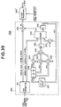
- Fig. 2 is a view showing the general configuration of a plasma display device for driving a plasma display panel (hereinafter designated “PDP") to allow it to emit light in accordance with the drive method of the first embodiment of the present invention.
- PDP plasma display panel
- an A/D converter 1 samples an analog input video signal in response to a clock signal supplied by the drive control circuit 2 to convert the video signal into, for example, 8-bit pixel data (input pixel data) D for each pixel. Then the data is supplied to the data converter 30.
- the drive control circuit 2 generates clock signals for the aforementioned A/D converter 1 and write/read signals for the memory 4 in synchronization with the horizontal and vertical synchronizing signals included in the aforementioned input video signal. Furthermore, the drive control circuit 2 generates various timing signals for controllably driving each of an address driver 6, a first sustain driver 7, and a second sustain driver 8 in synchronization with the horizontal and vertical synchronizing signals.
- the data converter 30 converts the 8-bit pixel data D into 8-bit converted pixel data (display pixel data) HD which is in turn supplied to the memory 4. Incidentally, the conversion operation of the data converter 30 is to be described later.
- the memory 4 performs writing sequentially the converted pixel data HD mentioned above in accordance with write signals supplied by the drive control circuit 2. After data for one screen (n rows and m columns) has been written through the write operation, the memory 4 divides the converted pixel data HD 11-nm for one screen into each bit digit for reading, which is in turn supplied sequentially to the addressing driver 6 for each one line.
- the addressing driver 6 generates, in accordance with a timing signal supplied by the drive control circuit 2, m pulses of pixel data having voltages corresponding to respective logic levels of the converted pixel data bits for a line which are read from the memory 4. These pulses are applied to column electrodes D 1 to D m of PDP 10, respectively.
- the PDP 10 comprises the aforementioned column electrodes D 1 to D m as address electrodes, and row electrodes X 1 to X n and row electrodes Y 1 to Y n , which are disposed orthogonal to the column electrodes.
- the PDP 10 allows a pair of a row electrode X and a row electrode Y to form a row electrode corresponding to one line. That is, in the PDP 10, the row electrode pair of the first line consists of row electrodes X 1 and Y 1 and the row electrode pair of the nth line consists of row electrodes X n and Y n .
- the aforementioned pairs of row electrodes and column electrodes are coated with a dielectric layer exposed to a discharge space, and each row electrode pair and column electrode are configured so as to form a discharge cell corresponding to one pixel at their intersection.
- the first and second sustain drivers 7 and 8 generate the various drive pulses, respectively, which are to be explained below. These pulses are in turn applied to the row electrodes X 1 to X n and Y 1 to Y n of the PDP 10.
- Fig. 3 is a view showing the application timing of various drive pulses which are applied to the column electrodes D 1 to D m , and the row electrodes X 1 to X n and Y 1 to Y n by the aforementioned address driver 6, and the first and second sustain drivers 7 and 8, respectively.
- a display period of one field is divided into 8 sub-fields SF1 to SF8 to drive the PDP 10.
- the pixel data writing step Wc is performed to write pixel data to each discharge cell of the cells.
- the light-emission sustaining step Ic is also performed in each of the sub-fields to sustain light-emission of only light-emitting cells mentioned above for a period (the number of times) corresponding to the weight assigned to each sub-field.
- the simultaneous reset process Rc for initializing all discharge cells of the PDP 10 is performed and the erase process E is executed only in the last sub-field SF8.
- the first and second sustain drivers 7 and 8 apply simultaneously the reset pulses RP X and RP Y shown in Fig. 3 to the row electrodes X 1 to X n and Y 1 to Y n of the PDP 10, respectively.
- the application of these reset pulses RP X and RP Y will cause all discharge cells of the PDP 10 to be reset and discharge, forming a predetermined uniform wall charge in each of the discharge cells. This will set all discharge cells of the PDP 10 to the aforementioned light-emitting cells.
- the address driver 6 applies sequentially pixel data pulse groups DP1 1-n , DP2 1-n , DP3 1-n , DP1 1-n ...DP8 1-n for respective lines to the column electrodes D 1 to D m as shown in Fig. 3. That is, in the sub-field SF1, the address driver 6 applies sequentially a pixel data pulse group DP1 1-n to the column electrodes D 1 to D m for each one of the lines to the column electrodes D 1 to D m as shown in Fig. 3.
- Said pixel data pulse group DP1 1-n corresponds to each of the first to the nth line and is generated in accordance with the first bit of each of the aforementioned converted pixel data HD 11-nm .
- the address driver 6 applies sequentially a pixel data pulse group DP2 1-n to the column electrodes D 1 to D m for each one of the lines to the column electrodes D 1 to D m as shown in Fig. 3, said pixel data pulse group DP2 1-n being generated in accordance with the second bit of each of the aforementioned converted pixel data HD 11-nm .
- the address driver 6 generates high-tension pixel data pulses to apply them to the column electrodes D only when the bit logic of the converted pixel data is, for example, a logic level of "1".
- the second sustain driver 8 generates the scan pulses SP shown in Fig. 3 to apply them in sequence to the row electrodes Y 1 to Y n at the same time as the application timing of each of the pixel data pulse groups.
- discharge selective erase discharge
- the wall charges remaining within the discharge cells are selectively erased.
- the selective erasing discharge causes the discharge cells that have been initialized into the light-emitting status at the aforementioned simultaneous reset process Rc to change to the non-light-emitting state.
- no discharge is generated in the discharge cells that are formed in the "columns" to which the aforementioned high-tension pixel data pulse has not been applied but to the state of being initialized at the aforementioned simultaneous reset process Rc, that is, the light-emitting state is sustained.
- the pixel data writing step Wc is performed so that the light-emitting cells where the light-emitting state is sustained at the light-emitting sustain process to be described later and the non-light-emitting cells where an off state remains are set alternatively in accordance with pixel data. That is, pixel data is written to each of the discharge cells.
- the first and second sustain drivers 7 and 8 apply the sustain pulses IP X and IP Y to the row electrodes X 1 to X n and Y 1 to Y n as shown in Fig. 3.
- the discharge cells where wall charges remain by the aforementioned pixel data writing step Wc that is, the light-emitting cells repeat discharge and light-emission to sustain their light-emitting state over the period of application of the sustain pulses IP X and IP Y thereto.
- the light-emission sustaining period (the number of times) is set corresponding to the weight assigned to each sub-field.
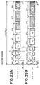
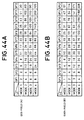
- Figs. 4A and 4B are views showing light-emission drive formats in which a light-emission sustaining period (the number of times) for each of the sub-fields is described.
- the drive mode (A) of Fig. 4A is employed, for example, in light-emission drive of even fields (or even frames), while the drive mode (B) of Fig. 4B is employed in light-emission drive of odd fields (or odd frames). light-emission drive of odd fields (or odd frames).
- the light-emitting period in the light-emission sustaining step Ic of each of the sub-fields SF1 to SF8 is set as follows as shown in the drive mode (A):
- the light-emitting period in the light-emission sustaining step Ic of each of the sub-fields SF1 to SF8 is set as follows as shown in the drive mode (B):
- each light-emission sustaining step Ic only those discharge cells that have been set to light-emitting cells in the pixel data writing step Wc performed immediately before the process Ic emit light over the light-emitting period shown in the drive mode (A) during the display period of an even field and in the drive mode (B) during the display period of an odd field.
- the address driver 6 generates an erase pulse AP to apply it to respective column electrodes D 1-m .
- the second sustain driver 8 generates the erase pulse EP simultaneously at the application timing of the erase pulse AP to apply it to respective row electrodes Y 1 to Y n .
- This simultaneous application of the erase pulses AP and EP causes erase discharge to be generated in all discharge cells of the PDP 10, allowing wall charges remaining within all discharge cells to disappear.
- executing the erase process E causes all discharge cells of the PDP 10 to be turned to non-light-emitting cells.
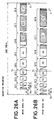
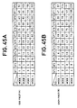
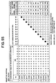
- Fig. 5 is a view showing all patterns of the light-emission drives to be performed in accordance with the light-emission drive formats shown in Figs. 4A and 4B.
- the selective erase discharge is performed (shown by black circles) for respective discharge cells only at the pixel data writing step Wc in one sub-field of the sub-fields SF1 to SF8. That is, the wall charges formed within all discharge cells of the PDP 10 by the execution of the simultaneous reset process Rc remain until the aforementioned selective erase discharge is performed.
- the charges promote discharge light-emission (shown by white circles) at the light-emission sustaining step Ic present over that period in respective sub-fields SF. That is, each of the discharge cells acts as light-emitting cells in the sub-fields shown by the black circles in Fig. 5 until the aforementioned selective erase discharge is performed.
- the discharge cell continues light-emission at the ratio of the light-emission periods shown in Figs. 4A and 4B at the light-emission sustaining step Ic in respective sub-fields present until then.
- the number of times at which respective discharge cells change from a light-emitting cell to a non-light-emitting cell is made equal to one or less in one field period without exception. That is, in one field period, such a light-emission drive pattern is prohibited that allows a discharge cell that has been set to a non-light-emitting cell to be restored to a light-emitting cell.
- the aforementioned simultaneous reset operation that accompanies intense light-emission irrespective of whether no involvement in displaying picture images may be performed once in one field period as shown in Fig. 3, and Figs. 4A and 4B, thereby allowing for preventing degradation in contrast.
- the selective erase discharge is performed only once at most within one field period as shown by the black circles of Fig. 5, thereby allowing for reducing power consumption thereof.
- no such light-emitting pattern exists that allows a period of the light-emitting state (shown by white circles) of a discharge cell and a period of a non-light-emitting state to be inverted to each other in one field period, so that a quasi-contour can be prevented.
- the light-emission drive pattern shown in Fig. 5 allows the light-emission drive to be performed to express a brightness of 9 levels of halftone at the following light-emission brightness ratio as shown by the light-emission brightness (L A ) during a display period of an even field. That is, ⁇ 0: 3: 14: 34: 64: 104: 155: 218: 255 ⁇ .
- the light-emission drive is performed to express brightness of 9 levels of halftone at the following light-emission brightness ratio as shown by the light-emission brightness (L B ). That is, ⁇ 0: 1: 7: 23: 47: 82: 128: 185: 255 ⁇ .
- Fig. 6 is a view showing the internal configuration of the data converter 30 shown in Fig. 2.
- the data converter 30 comprises an ABL circuit 31, a first data converter 32, a multi-level gray scale processing circuit 33, and a second data converter 34.
- the ABL (automatic brightness control) circuit 31 tunes the brightness level of the pixel data D of respective pixels supplied sequentially by the A/D converter 1 so that the average brightness of the pixels displayed on the screen of the PDP 10 falls within the predetermined range of brightness. Then, the ABL circuit 31 supplies the brightness tuning pixel data D BL obtained at this time to the first data converter 32.
- the tuning of brightness levels is carried out by setting the ratio of the number of times of light-emissions of sub-fields non-linearly before the inverse Gamma compensation is performed.
- the ABL circuit 31 tunes automatically the brightness level of the aforementioned pixel data D in response to the average brightness of the inverse-Gamma-converted pixel data obtained by applying the inverse Gamma compensation to the pixel data D (input pixel data). This allows for preventing degradation of the display quality caused by the brightness adjustment.
- Fig. 7 is a view showing the internal configuration of the ABL circuit 31.
- the level tuning circuit 310 outputs the brightness-tuning pixel data D BL obtained by tuning the level of the pixel data D in response to the average brightness determined by the average brightness detection circuit 311 which is to be described later.
- the average brightness detection circuit 311 determines the average brightness based on the inverse-Gamma-converted pixel data Dr and then supplies the average brightness to the aforementioned level tuning circuit 310.
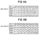
- the average brightness detection circuit 311 selects a brightness mode which causes the PDP 10 to emit light at an average brightness corresponding to the aforementioned average brightness, for example, from brightness modes 1 to 4 shown in Fig. 9A and 9B. Then, the average brightness detection circuit 311 supplies the brightness mode signal LC that shows the brightness mode selected to the drive control circuit 2. Incidentally, the average brightness detection circuit 311 selects use of the drive mode (A) of Fig. 9A for displaying even fields, while using the drive mode (B) of Fig. 9B for displaying odd fields.
- the drive control circuit 2 sets the period (i.e., the number of times of application of sustain pulses IP) during which light emission should be sustained in the light-emission sustaining step Ic of respective sub-fields SF1 to SF8 shown in Figs. 4A and 4B in accordance with the brightness mode signal LC shown in Figs. 9A and 9B.
- the period of light-emission at each sub-field shown in Figs. 4A and 9B shows the light-emission period when the brightness mode 1 is set.
- light-emission drive is performed at each sub-field for the following period of light emission.
- the first data converter 32 of Fig. 6 converts the brightness-tuning pixel data D BL of a 256-level gray scale and 8 bits, which is supplied by the aforementioned ABL circuit 31, into the converted pixel data HD P of 8 bits (0 to 128). Then, the data converted pixel data HD P is supplied to the multi-level gray scale processing circuit 33.
- Fig. 10 is a view showing the internal configuration of the first data converter 32.
- a data converter 321 converts the aforementioned brightness-tuning pixel data D BL into the converted pixel data A of 8 bits (0 to 128), in accordance with the conversion characteristics shown in Fig. 11, which is in turn supplied to a selector 322.
- a data converter 323 converts the aforementioned brightness-tuning pixel data D BL into the converted pixel data B of 8 bits (0 to 128), in accordance with the conversion characteristics shown in Fig. 12, which is in turn supplied to the selector 322. More specifically, the data converters 321 and 323 convert the brightness-tuning pixel data D BL into the converted pixel data A and B in accordance with the conversion tables shown in Fig. 13 and Fig.
- the selector 322 alternatively selects one of the converted pixel data A and B which corresponds to the logic level of a conversion characteristics selective signal and outputs one of the converted pixel data A or B as the converted pixel data HD P .
- the conversion characteristics selective signal is a signal that is supplied by the drive control circuit 2 shown in Fig. 2 and shifts, in response to the vertical synchronization timing of the input pixel data D, from logic level "1" to "0" or "0" to "1” .
- the conversion characteristics of Fig. 11 are paired with the drive mode (B) of Fig. 4B and the conversion characteristics of Fig.
- the selector 322 selects the converted pixel data B in a field (an even field) in which the drive mode (A) of Fig. 4A is set.
- the converted pixel data A is selected in a field (an odd field) to which the drive mode (B) of Fig. 4B is set.
- the data A and B is outputted as converted pixel data HD P .
- the aforementioned Conversion characteristics are set in accordance with the number of bits of input pixel data, the number of compressed bits resulting from multi-level gray scale processing, and the number of gray scale levels for display.
- the first data converter 32 is provided at the front stage of the multi-level gray-scale processing circuit 33 to be described later.
- This allows for performing conversion into the number of gray-scale levels for display and the number of compressed bits resulting from multi-level gray scale processing.
- This allows the brightness-tuning pixel data D BL to be divided at a bit boundary into an upper bit group (corresponding to multi-level gray scale pixel data) and a lower bit group (data to be discarded, error data).
- the multi-level gray scale processing is to be performed. This allows for preventing the occurrence of flat portions, caused by the occurrence of brightness saturation resulting from the multi-level gray scale processing and the absence of display levels of gray scale at a bit boundary, in the display characteristics (that is, the occurrence of disorder in gray scale levels).
- the configuration shown in Fig. 10 allows the first data converter 32 to switch the conversion characteristics (Fig. 11 and Fig. 12) of the brightness-tuning pixel data D BL of 8 bits (0 to 255) supplied by the aforementioned ABL circuit 31 at each one field (frame). At the same time, the first data converter 32 converts the brightness-tuning pixel data D BL into the converted pixel data HD P of 8 bits (0 to 128) which is in turn supplied to the multi-level gray-scale processing circuit 33.
- Fig. 15 is a view showing the internal configuration of the multi-level gray scale processing circuit 33.
- the multi-level gray scale processing circuit 33 comprises an error diffusion processing circuit 330 and dither processing circuit 350.
- the data separation circuit 331 of the error diffusion processing circuit 330 separates the lower 2 bits of the 8-bit converted pixel data HD P supplied by the aforementioned first data converter 32 into error data and the upper 6 bits into display data.
- the adder 332 supplies, to the delay circuit 336, an additional value obtained by adding the lower 2 bits as error data of the converted pixel data HD P , the delay output from the delay circuit 334, and a multiplication output of the scale multiplier 335.
- the delay circuit 336 causes an additional value supplied by the adder 332 to be delayed by the delay time D of the same length of time as the clock period of the pixel data. Then, the delay circuit 336 supplies the additional value to the aforementioned scale multiplier 335 and the delay circuit 337 as the delay additional signal AD 1 , respectively.
- the scale multiplier 335 multiplies the aforementioned delay additional signal AD 1 by the predetermined coefficient K 1 (for example, "7/16") and then supplies the result to the aforementioned adder 332.
- the delay circuit 337 causes further the aforementioned delay additional signal AD 1 to be delayed by the time (equal to one horizontal scan period - the aforementioned delay time D ⁇ 4) and then supplies the result to a delay circuit 338 as the delay additional signal AD 2 .
- the delay circuit 338 causes further the delay additional signal AD 2 to be delayed by the aforementioned delay time D and then supplies the resultant to a scale multiplier 339 as the delay additional signal AD 3 .
- the delay circuit 338 causes further the delay additional signal AD 2 to be delayed by the aforementioned delay time D ⁇ 2 and then supplies the result to a scale multiplier 340 as the delay additional signal AD 4 .
- the delay circuit 338 causes further the delay additional signal AD 2 to be delayed by the aforementioned delay time D ⁇ 3 and then supplies the result to a scale multiplier 341 as the delay additional signal AD 5 .
- the scale multiplier 339 multiplies the aforementioned delay additional signal AD 3 by the predetermined coefficient K 2 (for example, "3/16") and then supplies the result to an adder 342.
- the scale multiplier 340 multiplies the aforementioned delay additional signal AD 4 by the predetermined coefficient K 3 (for example. "5/16") and then supplies the result to the adder 342.
- the scale multiplier 341 multiplies the aforementioned delay additional signal AD 5 by the predetermined coefficient K 4 (for example, "1/16") and then supplies the result to the adder 342.
- the adder 342 supplies, to the aforementioned delay circuit 334, the additional signal that has been obtained by adding the results of multiplication supplied by the aforementioned respective scale multipliers 339, 340, and 341.
- the delay circuit 334 causes such additional signals to be delayed by the aforementioned delay time D and then supplies the resultant signal to the aforementioned adder 332.
- the adder 332 adds the aforementioned error data (lower two bits of the converted pixel data HD P ), the delay output from the delay circuit 334, and the output of multiplication of the scale multiplier 335. In this case, the adder 332 generates the carry-out signal C o which is equal to logic "0" in absence of carry and logic "1" in the presence of a carry and supplies the signal to an adder 333.
- the adder 333 adds the aforementioned display data (upper 6 bits of the converted pixel data HD P ) to the aforementioned carry-out signal C o and outputs the result as 6-bit error diffusion processing pixel data ED.
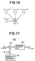
- the error diffusion processing pixel data ED corresponding to pixel G (j, k) of the PDP 10 shown in Fig. 16 is determined.
- the respective error data corresponding to pixel G (j, k-1) on the left of the pixel G (j, k), pixel G (j-1, k-1) on the upper left, pixel G (j-1, k) on the immediate above, and pixel G (j-1, k+1) on the upper right that is:
- the error diffusion processing circuit 330 interprets the upper 6 bits of the converted pixel data HD P as display data, and the remaining lower 2 bits as error data.
- the circuit also allows for adding the error data of the surrounding pixels ⁇ G (j, k-1), G (j-1, k+1), G (j-1, k), G (j-1, k-1) ⁇ by assigning weights thereto and the result is to be reflected to the aforementioned display data.
- This operation allows the brightness of the lower 2 bits at the original pixel ⁇ G (j, k) ⁇ to be expressed by the aforementioned surrounding pixels in an apparent manner. Therefore, this allows the display data of the number of bits less than 8 bits, that is, equal to 6 bits to express the levels of gray scale of brightness equivalent to those expressed by the aforementioned 8-bit pixel data.
- the coefficients K 1 to K 4 for error diffusion that should be assigned to the respective four pixels may be changed at each field.
- the dither processing circuit 350 applies the dither processing to the error diffusion processing pixel data ED supplied by the error diffusion processing circuit 330. This allows for generating the multi-level gray scale processing pixel data Ds whose number of bits is reduced further to 4 bits. Meanwhile, the dither processing circuit 350 maintains the level of gray scale of the same brightness as the 6-bit error diffusion processing pixel data ED. Incidentally, the dither processing allows a plurality of adjacent pixels to express one intermediate display level. Take as an example the case of display of a halftone corresponding to 8 bits by using the display data of the upper 6 bits out of an 8-bit pixel data. Four pixels to adjacent to each other at the left and right, and above and below are taken as one set.
- dither coefficients a to d having values different from each other are assigned to respective pixel data corresponding to each of the pixels in the set for addition.
- the dither processing is to produce four different combinations of intermediate display levels with four pixels. Therefore, even with the number of bits of the pixel data equal to 6 bits, the brightness levels of the gray scale available for display are 4 times, that is, a halftone display corresponding to 8 bits becomes available.
- a dither processing circuit 350 changes the dither coefficients a to d that should be assigned to the respective four pixels at each field.
- Fig. 17 is a view showing the internal configuration of the dither processing circuit 350.
- a dither coefficient generation circuit 352 generates four dither coefficients a, b, c, and d for each of the four pixels adjacent to each other and supplies these coefficients in sequence to the adder 351.
- dither coefficient generation circuit 352 changes, for each field as shown in Fig. 18, the aforementioned dither coefficients a, b, c, and d that should be assigned to the respective four pixels.
- dither coefficients a to d are assigned to the pixels at each field and generated repeatedly in a cyclic manner as shown below and supplied to the adder 351.
- the dither coefficient generation circuit 352 repeatedly executes the operation of the first to fourth fields mentioned above. That is, upon completion of generating the dither coefficients at the fourth field, the above-mentioned operation is repeated all over again from the aforementioned first field.
- the adder 351 adds the dither coefficients a to d which are assigned to respective fields as mentioned above to the error diffusion processing pixel data ED, respectively.
- the error diffusion processing pixel data ED corresponds to the aforementioned pixel G (j, k), pixel G (j, k+1), pixel G (j+1, k), and pixel G (j+1, k+1), respectively, which are supplied by the aforementioned error diffusion processing circuit 330.
- the adder 351 then supplies the dither additional pixel data thus obtained to the upper bit extracting circuit 353.
- each of the following data is supplied sequentially as the dither additional pixel data to the upper bit extracting circuit 353. That is,
- the upper bit extracting circuit 353 extracts the bits up to the upper four bits of the dither additional pixel data for output as multi-level gray scale pixel data D s .
- the dither processing circuit 350 shown in Fig. 17 changes the aforementioned dither coefficients a to d that should be associated with and assigned to each of the four pixels. This allows for determining the multi-level gray-scale pixel data D s of 4 bits (0 to 7) having a visually multi-level gray scale while reducing visual noise caused by dither patterns, which is then supplied to the second data converter 34.
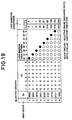
- the second data converter 34 converts the multi-level gray-scale pixel data D s into the converted pixel data (display pixel data) HD of bits 1 to 8 corresponding to respective sub-fields SF1 to SF8 in accordance with the conversion table shown in Fig. 19.
- the bits with logic level "1" among the bits 1 to 8 of the converted pixel data HD indicate the selective erase discharge to be carried out in the pixel data writing step Wc at the sub-fields SF corresponding to the bits (indicated by black circles).
- the aforementioned converted pixel data HD is supplied to the address driver 6 via the memory 4 as shown in Fig. 2.
- the format of the converted pixel data HD is to take one of the 9 patterns shown in Fig. 19.
- the address driver 6 assigns each of bits 1 to 8 in the aforementioned converted pixel data HD to the respective sub-fields SF1 to SF8. Then, only when the bit logic is logic level "1", the address driver 6 generates a high-tension pixel data pulse at the pixel data writing step Wc in the associated sub-field and supplies the pulse to the column electrodes D of the PDP 10. This allows for generating the aforementioned selective erase discharge.
- each discharge cell emits light at light-emission period ratio shown in Figs. 4A and 4B in each sustaining light-emission process Ic of each of the successive sub-fields which are present during the period.
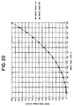
- Fig. 20 shows the relationship between the aforementioned two types of light-emission brightness (display brightness level) of 9 levels of halftone and the input pixel data D.
- symbols "- ⁇ -" and “- ⁇ -” show the relationship between the input pixel data D and display brightness level in the drive mode (A) and the drive mode (B), respectively.
- the drive pattern that is, the number of times of light-emission (the number of sustaining pulses) may be changes for each field (frame) in the light-emission sustaining step Ic of each sub-field.
- the figure shows that this allows the levels of halftone expressed by one drive mode to be interposed in between the levels of halftone expressed by the other drive mode.
- the effect of an integral with respect to time will provide the number of visual display levels of halftone greater than 9 levels of halftone and an improved gray-scale expression as such.
- a value between adjacent levels of halftone for example, a value between light-emission brightness "3" and "14" in the drive mode (A) is expressed by the multi-level gray-scale processing such as the aforementioned error diffusion processing and dither processing. (The value is a level corresponding to the lower 4 bits of the input pixel data D.)
- the multi-level gray-scale processing such as the error diffusion processing and dither processing
- a fewer number of original display levels of halftone causes patterns of the multi-level gray-scale processing to become conspicuous, providing a deteriorated S/N ratio.
- the light-emission drive pattern for each field (frame) can be changed to increase the number of visual display levels of halftone. Consequently, this will not allow patterns caused by the multi-level gray-scale processing to become conspicuous and thus provide an improved S/N ratio.
- Fig. 20 shows that the input pixel data D is inverse-gamma corrected by setting the ratio of the number of times of light-emission in the light-emission sustaining step Ic of each sub-field to the inverse gamma ratio.
- the drive modes (A) and (B) have 9 levels of halftone.
- the aforementioned combination of changing the light-emission drive pattern at each field (frame) and the multi-level gray-scale processing provides visual levels of halftone equivalent to 256 levels of halftone.
- a discharge cell is to be changed from the light-emitting state to a non-light-emitting state once or less in one field period. Accordingly, the aforementioned simultaneous reset operation that accompanies intense light-emission irrespective of whether no involvement in displaying picture images may be performed once in one field period is as shown in Figs. 4A and 4B. This allows for preventing degradation in contrast and reducing power consumption.
- the aforementioned embodiment described the case where the so-called selective erase addressing method was employed as a pixel data write method.
- the method allows for forming wall charges on each discharge cell in advance at the head of a field to set all discharge cells to light-emitting cells. Then, the wall charges are selectively erased in response to pixel data for writing the pixel data.
- the present invention is also applicable to the case where the so-called selective write addressing method is employed as the pixel data write method which allows for forming wall charges selectively in response to pixel data.
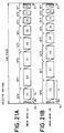
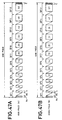
- Figs. 21A and 21B are views showing the light-emission drive format for the case where this selective write addressing method is employed.
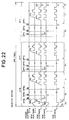
- Fig. 22 shows the application timing of various types of drive pulses to be applied to the column electrodes D 1 to D m , and the row electrodes X 1 to X n , Y 1 to Y n of the PDP 10 in accordance with the light-emission drive formats shown in Fig. 21A and 21B.
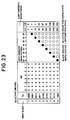
- Fig. 23 shows the conversion table for use in the second data converter 34 for the case where the selective write addressing method is employed, and all patterns of the light-emission drive to be carried out in one field period.
- the aforementioned selective write addressing method when employed initially allows the first and second sustain drivers 7 and 8 to apply the reset pulses RP x and RP y simultaneously to row electrodes X and Y, respectively, at the simultaneous reset process Rc of the head sub-field SF8.
- This causes all discharge cells of the PDP 10 to carry out reset discharge and thus forces wall charges to be built up within each of the discharge cells (R 1 ).
- the first sustain driver 7 applies simultaneously the erase pulse EP to the row electrodes X 1 to X n of the PDP 10, thereby erasing the aforementioned wall charges formed in all discharge cells (R 2 ). That is, the simultaneous reset process Rc shown in Fig. 22 is carried out to reset all discharge cells of the PDP 10 to the state of non-light-emitting cells.
- the pixel data writing step Wc allows only those discharge cells located at the intersections of the "rows" to which the scan pulse SP is applied and the "columns” to which a high-tension pixel data pulse is applied to produce discharge (selective write discharge). This results in selectively building up wall charges in the discharge cells.
- the selective write discharge causes the discharge cells that have been reset to the state of non-light-emitting cells at the aforementioned simultaneous reset process Rc to change into the state of light-emitting cells.
- the pixel data writing step Wc is carried out for selectively setting to either the light-emitting cell of which the light-emitting state is sustained during the light-emission sustaining step to be described later or the non-light-emitting cell remaining in an "off" state.
- the so-called writing of pixel data to each discharge cell is performed.
- the light-emission drive by the selective write addressing method will cause the selective write discharge to be carried out only at those sub-fields SF corresponding to the bits of logic level "1" of the converted pixel data HD as shown in Fig. 23 (indicated by black circles).
- the non-light-emitting state is sustained at the sub-fields present during a period until the selective write discharge is carried out from the head sub-field SF8.
- the light-emitting state is sustained at the sub-fields SF (indicated by white circles) except for the sub-fields SF (indicated by black circles) for which the selective write discharge has been carried out and the sub-fields present thereafter.
- the drive methods shown in Fig. 3 through Fig. 23 allow for resetting all discharge cells to either one of a light-emitting cell or non-light-emitting cell only at the head sub-field of one field period.
- pixel data is written to set each discharge cell to a light-emitting or non-light-emitting cell in response to the pixel data.
- the drive method allows the sub-fields of a field to enter the light-emitting state from the head sub-field in sequence with increasing brightness to be displayed.
- the selective write addressing method allows the sub-fields of a field to enter the light-emitting state from the last sub-field in sequence with increasing brightness to be displayed.
- the present invention allows for performing, in alternate fields (frames), two types of light-emission drives having different periods of light-emission (the number of times) at each sub-field, for example, the drive modes (A) and (B) shown in Figs. 4A and 4B.
- this allows for increasing the number of visual brightness levels of halftone.
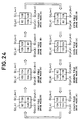
- Fig. 24 is a view showing a specific operation of the aforementioned drive methods shown in Fig. 3 through Fig. 23.
- the inverse Gamma compensation provides the display brightness of approximately "116".
- the drive mode (B) of Fig. 4B and the conversion characteristics of Fig. 11 are selected in the first field (an odd field), and the multi-level gray-scale processing provides the following display brightness. That is, for example,
- display brightness "116" is expressed by the average brightness of four pixels adjacent up and down and the left and right.
- the drive mode (A) of Fig. 4A and the conversion characteristics of Fig. 12 are selected in the second field (an even field), and multi-level gray-scale processing provides the following display brightness. That is, for example,
- display brightness "116" is expressed by the average brightness of four pixels adjacent up and down and the left and right.
- the two types of light-emission drives having light-emission periods different from each other are performed alternately at each field (frame) as mentioned above. This may cause the center of gravity of the light-emission in one field period to be displaced, resulting in and the occurrence of flicker.
- the center of gravity of light-emission is determined based on the length of the pixel data writing step of a sub-field in the light-emitting state during one field period, the length of the light-emission sustaining step, and the weight assigned to the light-emission period.
- Figs. 25A and 25B show diagrammatically the displacement of the center of gravity of light-emission at even and odd fields.
- both even fields of the drive mode (A) and odd fields of the drive mode (B) have approximately the same average display brightness, however, the displacement of the center of gravity of light-emission causes flicker to be produced.
- Figs. 26A, 26B and Figs. 27A, 27B show an example of the light-emission drive format provided to prevent the flickering, respectively.
- the light-emission drive formats shown in Figs. 26A and 26B allow the start-up timing of the light-emission drive shown in the drive mode (A) to be delayed by a predetermined period ⁇ T relative to the start-up timing of the light-emission drive shown in the drive mode (B). This provides less displacement between both centers of gravity of light-emission T 1 and T 2 and thus reduces flicker.
- the flicker is more conspicuous at a higher display brightness.
- the aforementioned predetermined period ⁇ T is set to such a constant value that allows the center of gravity of light-emission T 1 in the drive mode (A) to correspond with the center of gravity of light-emission T 2 in the drive mode (B), at the maximum display brightness level "255".
- the displacement between the center of gravity of light-emission T 1 in the drive mode (A) and the center of gravity of light-emission T 2 in the drive mode (B) varies with the display brightness level. That is, the displacement takes the maximum value at the maximum display brightness level, while the displacement becomes less with a decreasing display brightness level.
- the variation in the displacement caused by this display brightness level is small and small level of display brightness allows flickering to be less conspicuous.
- the aforementioned predetermined period ⁇ T may be varied so that the centers of gravity of light-emission always coincides with each other.
- the light-emission drive formats shown in Figs. 27A and 27B allow the execution period Ta of the pixel data writing step Wc of each of the sub-fields SF1 to SF4 in the drive mode (A) to be longer than the execution period Tb of the pixel data writing step Wc in the drive mode (B).
- This allows for providing less displacement between the centers of gravity of light-emission T 1 and T 2 to reduce flicker.
- the pulse width of the scan pulse SP to be applied to the row electrodes of the PDP 10 is widened in the pixel data writing step Wc of each of the sub-fields SF1 to SF4 in the drive mode (A). This allows for making the execution period Ta longer than the execution period Tb.
- the two types of light-emission drives of which light-emission periods are different for each other at each sub-field are to be switched at alternate fields (frames).
- the switching may be carried out at alternate lines of the PDP 10.
- Figs. 28A and 28B show an example of the light-emission drive formats developed in view of the aforementioned point.
- the selective erase discharge is carried out at all lines of the PDP 10 in the pixel data writing step W AC .
- the selective erase discharge is carried out only at even lines of the PDP 10 in the pixel data writing step W 1C
- the selective erase discharge is carried out only at the odd lines in the pixel data writing step W 2C .
- the light-emission drive is carried out in each sub-field at the following light-emission period ratio according to the drive mode (A) of Fig. 28A. That is,
- the light-emission drive is carried out in each sub-field at the following light-emission period ratio according to the drive mode (B) of Fig. 28B. That is,
- the two types of light-emission drives having light-emission periods different from each other at each sub-field may be carried out at alternative fields (frames) and at alternative lines of the PDP 10.
- the selective erase discharge is carried out only at the discharge cells of the even lines of the PDP 10 during the display period of odd frames. Additionally, the selective erase discharge is carried out only at the discharge cells of the odd lines during the display period of even frames.
- the selective erase discharge is carried out only at the discharge cells of the odd lines of the PDP 10 during the display period of odd frames. Additionally, the selective erase discharge is carried out only at the discharge cells of the even lines during the display period of even frames.
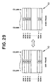
- Fig. 29 shows the format of light-emission drive that is carried out by the aforementioned drive.
- light-emission drive is carried out at the discharge cells of the even lines of the PDP 10 in accordance with the drive mode (A) of Fig. 25A.
- light-emission drive is carried out at the discharge cells of the odd lines in accordance with the drive mode (B) of Fig. 25B.
- light-emission drive is carried out at the discharge cells of the even lines of the PDP 10 in accordance with the drive mode (B) of Fig. 25B.
- light-emission drive is carried out at the discharge cells of the odd lines in accordance with the drive mode (A) of Fig. 25A.
- This drive allows for preventing flicker caused by carrying out the two types of light-emission drive at alternate fields (frames) such as the drive modes (A) and (B), of which light-emission periods are different from each other.
- the drive mode to be changed at each field (frame) or each line is not limited to the aforementioned two types.
- three or more types of drive modes having light-emission periods different from each other at respective sub-fields may be prepared and switched in sequence at each field (frame) or at each line for carrying out a light-emission drive.
- the selective erase (write) discharge is to be generated by the simultaneous application of the scan pulse SP and the high-tension pixel data pulse in one of the pixel data writing stepes Wc of the sub-fields SF1 to SF8.
- a lower amount of charged particles remaining in discharge cells may cause the selective erase (write) discharge to be generated in a normal manner regardless of the simultaneous application of the scan pulse SP and the high-tension pixel data pulse. This may cause the wall charges in the discharge cells not to be erased (built up) in a normal manner.
- the converted pixel data HD has the following value at the time of employing the selective erase addressing method as the pixel data write method, that is, [01000000].
- the selective erase discharge is carried out only at the sub-field SF2, during which the discharge cells are changed to non-light-emitting cells.
- the selective erase fails at the sub-field SF2 to cause the wall charge to remain in the discharge cell
- the sustaining light-emission is carried out not only at the sub-field SF1 but also at the subsequent sub-fields SF2 to SF8. Consequently, this leads to the maximum brightness display.
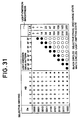
- Fig. 30 shows a light-emission drive format used when the selective erase addressing method is employed
- Fig. 31 shows a light-emission drive format used when the selective write addressing method is employed, respectively.
- the "*" shown in Fig. 30 and Fig. 31 indicates that any one of logic level “1” or “0” may be selected, and the triangular mark indicates that the selective erase (write) discharge is carried out only when the "*" is logic level "1".
- the selective erase (write) discharge is repeated at least in one of the subsequent sub-fields. This ensures pixel data writing and prevents accidental light-emission.
- the method for driving a plasma display panel can provide improved expression of levels of halftone as well as improved display quality. Furthermore, the method can provide improved contrast as well as prevent quasi-contour and reduce power consumption.
- Fig. 32 is a view showing the general configuration of a plasma display device for driving a plasma display panel (hereinafter designated "PDP") to allow it to emit light in accordance with the drive method of a second aspect of the present invention.
- PDP plasma display panel
- the plasma display device comprises a drive portion having an operating unit 5, a drive control circuit 2, an input selector 3, an A/D converter 1, a data converter 300, a memory 4, an addressing driver 6, a first sustain driver 7, and a second sustain driver 8.
- the device also comprises a PDP 10 as a plasma display panel.
- the plasma display device supports video signals from personal computers, that is, the PC video signal, as well as television signals of the NTSC scheme, and is provided with separate input terminals (not shown) specifically designed for inputting respective video signals of these different schemes.
- the operating unit 5 generates the input-designated video signal Sv corresponding to the video signal designated by the user for input, and then supplies the signal Sv to the drive control circuit 2, the input selector 3, and the data converter 300, respectively.
- the operating unit 5 generates, for example, the input-designated video signal Sv of logic level "0" when the user has designated the aforementioned PC video signal as the video signal to be displayed.
- the unit 5 generates the input-designated video signal Sv of logic level "1" when the user has designated the color television signal (hereinafter called the "TV signal").
- the input selector 3 selects either the PC video signal supplied via the aforementioned input terminals or the TV signal, whichever one corresponds to the aforementioned input-designated video signal Sv and is in turn supplied to the A/D converter 1 as an input video signal.
- the PC video signal and the TV signal are Gamma-corrected in advance.
- the A/D converter 1 samples the input video signal supplied from the aforementioned input selector 3 in response to the clock signal supplied from the drive control circuit 2 and then converts the input video signal, for example, into the pixel data D of 8 bits. That is, the A/D converter 1 converts the analog input video signal supplied from the input selector 3 into the 8-bit pixel data that is allowed for expressing brightness with 256 levels of halftone.
- the data converter 300 converts, corresponding to the 8-bit pixel data D, the data obtained through the brightness tuning and multi-level gray-scale processing, respectively, into the display drive pixel data GD for actually driving respective pixels of the PDP 10. Then, the data converter 300 supplies the display drive pixel data GD to the memory 4.
- Fig. 33 is a view showing the internal configuration of the data converter 300.
- the data converter 300 comprises an ABL (automatic brightness control) circuit 301, a first data converter 302, a multi-level gray-scale processing circuit 303, and a second data converter 304.
- ABL automatic brightness control
- the ABL circuit 301 tunes the brightness level of the pixel data D of each pixel supplied in sequence from the A/D converter 1 so that the average brightness of a picture image displayed on the screen of the PDP 10 falls within an adequate brightness range. Then, the ABL circuit 301 supplies the brightness-tuning pixel data D BL thus obtained to the first data converter 302.
- Fig. 34 is a view showing the internal configuration of the ABL circuit 301.
- the ABL circuit 301 has the same configuration as that of the ABL circuit 31 shown in Fig. 7.
- the level tuning circuit 310 outputs the brightness-tuning pixel data D BL obtained by tuning the level of the pixel data D based on the average brightness determined at an average brightness detection circuit 311 to be described later.
- the average brightness detection circuit 311 determines the inverse-Gamma-converted pixel data Dr first. At this stage, the average brightness detection circuit 311 determines which brightness mode the average brightness corresponds to among the brightness modes 1 to 4. The modes are the four levels into which the range between the maximum and the minimum brightness has been divided.
- the average brightness detection circuit 311 supplies the average brightness determined as mentioned above to the aforementioned level tuning circuit 310, while supplying the brightness mode signal LC that indicates the corresponding brightness mode to the drive control circuit 2. That is, the level tuning circuit 310 supplies the pixel data D to which level has been tuned according to the average brightness, as the aforementioned brightness-tuned pixel data D BL , to the aforementioned data converter 312 and the subsequent first data converter 32.
- Fig. 36 is a view showing the internal configuration of the first data converter 302.
- the data converter 321' converts the aforementioned brightness-tuned pixel data D BL into 8-bit converted pixel data A 1 having "0" to "192” in accordance with the conversion characteristics shown in Fig. 37A, which is in turn supplied to the selector 322.
- the data converter 323' converts the aforementioned brightness-tuned pixel data D BL into 8-bit converted pixel data B 1 having "0" to "192” in accordance with the conversion characteristics shown in Fig. 37B, which is in turn supplied to the selector 322.
- the selector 322 selects in an alternative manner either one of the converted pixel data A 1 or B 1 , whichever one that corresponds to the logic level of the conversion characteristics selective signal and is in turn supplied to a selector 324.
- the aforementioned conversion characteristics selective signal is a signal which is supplied from the aforementioned drive control circuit 2 and changes from logic level “1" to "0” or from “0” to “1” in response to the vertical synchronization timing of the input video signal.
- a data converter 325 converts the aforementioned brightness-tuned pixel data D BL into 9-bit converted pixel data A 2 having "0" to "384" in accordance with the conversion characteristics shown in Fig. 38A, which is in turn supplied to a selector 326.
- a data converter 327 converts the aforementioned brightness-tuned pixel data D BL into 9-bit converted pixel data B 2 having "0" to "384" in accordance with the conversion characteristics shown in Fig. 38B, which is in turn supplied to the selector 326.
- the selector 326 selects in an alternative manner either one of the converted pixel data A 2 or B 2 , whichever one that corresponds to the logic level of the conversion characteristics selective signal and is in turn supplied to a selector 324.
- the selector 324 selects in an alternative manner either one of the converted pixel data A 1 (or B 1 ) supplied from the selector 322 or the converted pixel data A 2 (or B 2 ) supplied from the selector 326, whichever one that corresponds to the logic level of the input-designated video signal Sv. Then, the selector 324 supplies the data to the subsequent multi-level gray-scale processing circuit 33 as the first converted pixel data D H .
- the first data converter 302 converts the brightness-tuned pixel data D BL of 8 bits of "0" to "255” into the first converted pixel data D H of 8 bits of "0" to "192". The conversion is carried out based on the conversion characteristics shown in Figs. 37A and 37B, and then the first converted pixel data DH is supplied to the multi-level gray-scale processing circuit 303.
- the brightness-tuned pixel data D BL of 8 bits of "0" to "255” is converted into the first converted pixel data D H of 9 bits of "0" to "384".
- Fig. 37A and Fig. 38A show the conversion characteristics used for displaying odd fields (odd frames), while Fig. 37B and Fig. 38B show the conversion characteristics used for displaying even fields (even frames). That is, when the TV signal is designated as an input, the first data converter 302 switches the conversion characteristics used for the conversion thereof at each field (frame) as shown in Figs. 37A and 37B. On the other hand, when the PC video signal is designated as an input, the conversion characteristics used for the conversion thereof are switched at each field as shown in Figs. 38A and 38B.
- the first data converter 302 is provided at the preceding stage of the multi-level gray-scale processing circuit 303 to be described later. Then, data conversion is carried out to the number of display levels of halftone and the number of compressed bits resulting from the operation of the multi-level gray scale. This prevents the occurrence of flat portions, caused by the occurrence of brightness saturation resulting from the multi-level gray scale processing and absence of display levels of gray scale at a bit boundary, in the display characteristics (that is, the occurrence of disorder in gray scale levels).
- Fig. 39 shows the internal configuration of the multi-level gray-scale processing circuit 303.
- the multi-level gray-scale processing circuit 303 comprises the error-diffusion processing circuit 330 and the dither processing circuit 350. Since the configuration of the error-diffusion-processing circuit 330 is the same as that shown in Fig. 15, explanation is not repeated. P45
- the dither processing circuit 350 applies dither processing to the error-diffusion processing pixel data ED supplied by the error-diffusion processing circuit 330.
- This allows for generating the multi-level gray-scale pixel data D s having the number of bits further reduced to four, while maintaining brightness levels of halftone equivalent to the error-diffusion processing pixel data ED of 6 bits.
- dither processing expresses one intermediate display level by means of a plurality of adjacent pixels. Take as an example the case where pixel data of an upper 6 bits among 8-bit pixel data is used to express a gray scale display equivalent to an 8-bit expression. In this case, four pixels adjacent on the left and right, above and below, are taken as one set.
- dither coefficients a to d which have coefficient values different from each other, are assigned to the pixel data corresponding to the set of respective pixels and added, respectively.
- the dither processing generates four different combinations of intermediate display levels with four pixels. Therefore, even when the pixel data has 6 bits, it is allowed for expressing the intermediate display with four times the level of halftone, that is, 8-bit-equivalent intermediate display.
- the dither processing circuit 350 changes, at each field, with the aforementioned dither coefficients a to d that should be assigned to the respective four pixels.
- Fig. 40 shows the internal configuration of the dither processing circuit 350.
- the dither coefficient generating circuit 352' generates four dither coefficients a, b, c, and d, for four respective pixels that are adjacent to each other, which are in turn supplied to the adder 351 in sequence.
- the dither coefficient generating circuit 352' generates dither coefficients with different values in response to the designated input video signal indicated by the aforementioned input-designated video signal Sv.
- the video signal designated for input is the PC video signal
- the following dither coefficients a to d comprising three bits, respectively, are generated as shown in Fig. 41. That is,
- dither coefficients a to d are generated corresponding to four pixels, respectively.
- the four pixels are pixel G (j, k) and pixel G (j, k+1) corresponding to row j, and pixel G (j+1, k) and pixel G (j+1, k+1) corresponding to row (j+1).
- the dither coefficient generating circuit 352 changes, for each field as shown in Fig. 18, the aforementioned dither coefficients a to d that should be assigned to the respective four pixels.
- the dither coefficient generating circuit 352' generates the dither coefficients a to d repeatedly in a cyclic manner and supplies the coefficients to the adder 351.
- the dither coefficient generating circuit 352' executes repeatedly the operation of the first to fourth fields mentioned above. That is, upon completion of generating the dither coefficients at the fourth field, the above-mentioned operation is repeated all over again from the aforementioned first field.
- the adder 351 adds the dither coefficients a to d which are assigned to respective fields as mentioned above to the error diffusion processing pixel data ED, respectively.
- the error diffusion processing pixel data ED correspond to the aforementioned pixel G (j, k), pixel G (j, k+1), pixel G (j+1, k), and pixel G (j+1, k+1), respectively, which are supplied by the aforementioned error diffusion processing circuit 330.
- the adder 351 then supplies the dither additional pixel data thus obtained to the upper bit extracting circuit 353.
- each of the following data is supplied sequentially as the dither additional pixel data to the upper bit extracting circuit 353. That is,
- the upper bit extracting circuit 353 extracts the bits up to the upper four bits of the dither additional pixel data for output as multi-level gray scale pixel data D s .
- the dither processing circuit 350' shown in Fig. 39 changes the aforementioned dither coefficients a to d that should be associated with and assigned to each of the four pixels. This allows for determining the multi-level gray-scale pixel data D s of 4 bits having a visually multi-level gray scale while reducing visual noise caused by dither patterns, which is then supplied to the second data converter 34.
- the second data converter 34 converts the multi-level gray-scale pixel data D s into the display drive pixel data GD of bits 1 to 12 in accordance with the conversion table shown in Fig. 14.
- the respective bits 1 to 12 correspond to each of the sub-fields SF1 to SF12 to be described later.
- the data converter 30 comprises the ABL circuit 31, the first data converter 32, the multi-level gray-scale processing circuit 33, and the second data converter 34.
- the pixel data D that is capable of expressing 256 levels of halftone with 8 bits is converted into the display drive pixel data GD of 12 bits comprising 13 patterns in total as shown in Fig. 42.
- the memory 4 of Fig. 32 writes and stores sequentially the aforementioned display drive pixel data GD in accordance with the write signal supplied by the drive control circuit 2.
- the write action allows for writing the display drive pixel data GD 11-nm for one screen (with n rows and m columns).
- the memory 4 reads the display drive pixel data GD11-nm for each row by associating the same bit digit with each other, which is then supplied to the addressing driver 6. That is, the memory 4 regards the display drive pixel data GD 11-nm of one screen comprising 12 bits, respectively, as the 12-way-split display drive pixel data DB1 11-nm to DB12 11-nm shown as follows. That is,
- the memory 4 reads the data DB1 11-nm , DB2 11-nm , ...DB12 11-nm in sequence line by line in accordance with the read signal supplied by the drive control circuit 2 and then supplies the data to the addressing driver 6.
- the drive control circuit 2 generates clock signals for the aforementioned A/D converter 1 and write/read signals for the memory 4 in synchronization with the horizontal and vertical synchronizing signals included in the aforementioned input video signal. Furthermore, the drive control circuit 2 generates various timing signals for controllably driving each of an addressing driver 6, a first sustain driver 7, and a second sustain driver 8 in synchronization with the horizontal and vertical synchronizing signals.
- the addressing driver 6 generates, in accordance with a timing signal supplied by the drive control circuit 2, m pulses of pixel data having voltages corresponding to respective logic levels of the display drive pixel data bits DB for a line which are read from the memory 4. These pulses are applied to column electrodes D 1 to D m of PDP 10, respectively.
- the PDP 10 comprises the aforementioned column electrodes D1 to Dm as address electrodes, and row electrodes X 1 to X n and row electrodes Y 1 to Y n , which are disposed orthogonal to the column electrodes.
- the PDP 10 allows a pair of a row electrode X and a row electrode Y to form a row electrode corresponding to one line. That is, in the PDP 10, the row electrode pair of the first line consists of row electrodes X 1 and Y 1 and the row electrode pair of the nth line consists of row electrodes X n and Y n .
- the aforementioned pairs of row electrodes and column electrodes are coated with a dielectric layer exposed to a discharge space, and each row electrode pair and column electrode are configured so as to form a discharge cell corresponding to a pixel at their intersection.
- the first and second sustain drivers 7 and 8 generate the various drive pulses, respectively, which are to be explained below. These pulses are in turn applied to the row electrodes X 1 to X n and Y 1 to Y n of the PDP 10.
- Fig. 43 is a view showing the application timing of various drive pulses which are applied to the column electrodes D 1 to D m , and the row electrodes X 1 to X n and Y 1 to Y n by the aforementioned addressing driver 6, and the first and second sustain drivers 7 and 8, respectively.
- a display period of one field is divided into 12 sub-fields SF1 to SF12 to drive the PDP 10.
- the pixel data writing step Wc is performed to write pixel data to each discharge cell of the PDP 10 for setting "light-emitting cells" and "non-light-emitting cells".
- the light-emission sustaining step Ic is also performed in each of the sub-fields to sustain light-emission of the only "light-emitting cells" mentioned above for a period (the number of times) corresponding to the weight assigned to each sub-field.
- the simultaneous reset process Rc for initializing all discharge cells of the PDP 10 performed and the erase process E is executed only in the last sub-field SF12.
- the first and second sustain drivers 7 and 8 apply simultaneously the reset pulses RP X and RP Y shown in Fig. 43 to the row electrodes X 1 to X n and Y 1 to Y n of the PDP 10, respectively.
- the application of these reset pulses RP X and RP Y will cause all discharge cells of the PDP 10 to be reset and discharged, forming a predetermined uniform wall charge in each of the discharge cells. This will set all discharge cells of the PDP 10 to the aforementioned "light-emitting cells" for the time being.
- the addressing driver 6 generates a pixel data pulse having a voltage corresponding to the logic level of the display drive pixel data bit DB supplied by the aforementioned memory 4.
- the addressing driver 6 applies sequentially the data pulse to the column electrode D 1-m line by line. That is, first, in the pixel data writing step Wc of the sub-field SF1, DB1 11-1m which corresponds to the first line of the sub-field is extracted from the aforementioned display drive pixel data bit DB1 11-nm . Then, the pixel data pulse group DP1 1 comprising m pixel data pulses corresponding to the logic levels of the respective DB1 11-1m is generated and applied to the column electrode D 1-m .
- DB1 21-2m that corresponds to the second line of the sub-field is extracted from the display drive pixel data bit DB1 11-nm .
- the pixel data pulse group DP1 2 comprising m pixel data pulses corresponding to the logic levels of the respective DB1 21-2m is generated and applied to the column electrode D 1-m .
- the pixel data pulse groups DP1 3 to DP1 n for one line are applied to the column electrodes D 1-m in sequence.
- DB2 11-1m which corresponds to the first line of the sub-field is first extracted from the aforementioned display drive pixel data bit DB2 11-nm .
- the pixel data pulse group DP2 1 comprising m pixel data pulses corresponding to the logic levels of the respective DB2 11-1m is generated and applied to the column electrode D 1-m .
- DB2 21-2m that corresponds to the second line of the sub-field is extracted from the display drive pixel data bit DB2 11-nm .
- the pixel data pulse group DP2 2 comprising m pixel data pulses corresponding to the logic levels of the respective DB2 21-2m is generated and applied to the column electrode D 1-m .
- the pixel data pulse groups DP2 3 to DP2 n for one line are applied to the column electrodes D 1-m in sequence.
- the addressing driver 6 assigns the pixel data pulse groups DP3 1-n to DP12 1-n generated based on the respective display drive pixel data bits DB3 11-nm to DB12 11-nm to the sub-fields SF3 to SF12, respectively. Then, the addressing driver 6 applies the pixel data pulse groups DP3 1-n to DP12 1-n to the column electrodes D 1-m .
- the addressing driver 6 generates a high-tension pixel data pulse when the display drive pixel data bit DB has a logic level of "1", while generating a low-voltage (0 volt) pixel data pulse when the logic level is "0".
- the second sustain driver 8 generates the scan pulses SP of negative polarity shown in Fig. 43 at the same time as the application timing of each of the pixel data pulse groups DP as aforementioned. Then, the second sustain driver 8 applies the scan pulses SP in sequence to the row electrodes Y 1 to Y n . At this time, discharge (selective erase discharge) is caused only at the discharge cells located at the intersections of the "lines" to which the scan pulse SP is applied and the "columns" to which a high-tension pixel data pulse is applied. The wall charges remaining within the discharge cells are selectively erased.
- the respective 1 st to 12 th bits of the display drive pixel data GD determines whether the selective erase discharge should be generated in the pixel data writing step Wc of respective sub-fields SF1 to SF12.
- the selective erasing discharge causes the discharge cells that have been reset to the "light-emitting cell” at the aforementioned simultaneous reset process Rc to change to the "non-light-emitting cell".
- no discharge is generated in the discharge cells that are formed in the "columns" to which a low-voltage pixel data pulse is applied, and thus the preset state is sustained.
- discharge cells of "non-light-emitting cells” remain as “non-light-emitting cells”
- discharge cells of "light-emitting cells” remain as “light-emitting cells”.
- the immediately subsequent light-emission sustaining step Ic allows for setting "light-emitting cells” in which sustaining discharge is generated and “non-light-emitting cells” in which sustaining discharge is not generated owing to the pixel data writing step Wc for each sub-field.
- the first and second sustain drivers 7 and 8 apply the sustaining pulses IP X and IP Y of positive polarity alternately as shown in Fig. 43 to the row electrodes X 1 to X n and Y 1 to Y n , respectively.
- the number of times of application of the sustain pulses IP applied in the light-emission sustaining step Ic is set in accordance with the weight assigned to each sub-field. In addition, the number of times differs according to the type of brightness mode signal LC supplied from the data converter 30 shown in Fig. 32, and the video signal selected as the input video signal at the aforementioned input selector 3.
- Fig. 16 shows the number of times of application of the sustain pulses IP to be applied at the light-emission sustaining step Ic of respective sub-fields SF1 to SF12 when the TV signal is selected as an input video signal.
- Figs. 44A and 44B show the number of times of application of the sustain pulses IP to be applied when odd fields (odd frames) are displayed and when even fields (even frames) are displayed, respectively, for each mode according to the brightness mode signal LC.
- Fig. 45A shows the number of times of application of the sustain pulses IP to be applied at the light-emission sustaining step Ic of respective sub-fields SF1 to SF12 when the PC video signal is selected as an input video signal.
- Figs. 45A and 45B show the number of times of application of the sustain pulses IP to be applied when odd fields (odd frames) are displayed and when even fields (even frames) are displayed, respectively, for each mode according to the brightness mode signal LC.
- the drive control circuit 2 supplies various timing signals to the addressing driver 6, the first sustain driver 7, and the second sustain driver 8 in order to carry out actions according to the light-emission drive sequences shown in Figs. 46A and 46B.
- Figs. 46A and 46B show the light-emission drive sequences to be carried out for displaying odd fields (odd frames) and for displaying even fields (even frames), respectively.
- the ratio of the number of times of application of the sustain pulses IP at the light-emission sustaining step Ic of respective sub-fields SF1 to SF12 is as follows.
- the drive control circuit 2 supplies various timing signals to the addressing driver 6, the first sustain driver 7, and the second sustain driver 8 in order to carry out actions according to the light-emission drive sequences as shown in Figs. 47A and 47B.
- Figs. 47A and 47B show the light-emission drive sequences to be carried out for displaying odd fields (odd frames) and for displaying even fields (even frames), respectively.
- the ratio of the number of times of application of the sustain pulses IP at the light-emission sustaining step Ic of respective sub-fields SF1 to SF12 is as follows.
- the number of sub-fields responsible for low-brightness light-emission among the aforementioned respective sub-fields SF1 to SF12 is made larger than that of the sub-fields responsible for high-brightness light-emission.
- the sub-fields responsible for relatively low brightness light-emission for which the sustain pulse IP is applied 25 times or less are 8 sub-fields, from SF1 to SF8, and are greater in number than the sub-fields SF9 to SF12 that are responsible for high-brightness light-emission.
- the address driver 6 In the erase process E, the address driver 6 generates an erase pulse AP having positive polarity as shown in Fig. 43 to apply it to column electrodes D 1-m . Furthermore, the second sustain driver 8 generates the erase pulse EP having positive polarity simultaneously at the application timing of the erase pulse AP to apply it to respective row electrodes Y 1 to Y n .
- This simultaneous application of the erase pulses AP and EP causes erase discharge to be generated in all discharge cells of the PDP 10, allowing wall charges remaining within all discharge cells to disappear. That is, executing the erase discharge causes all discharge cells of the PDP 10 to be changed to "non-light-emitting cells"
- each discharge cell at each sub-field is set to a "light-emitting cells" or "non-light-emitting cell". That is, each bit 1 to 12 of the display drive pixel data GD corresponds to sub-fields SF1 to SF12, respectively.
- the selective erase discharge is generated in the pixel data writing step Wc of the sub-field corresponding to the digit of the bit and thus the discharge cell is set to the "non-light-emitting cell".
- the bit has logic level "0”
- the aforementioned selective erase discharge is not generated and thus the present state is sustained.
- the discharge cell of a "non-light-emitting cell” remains as a "non-light-emitting cell", while the discharge cell of a "light-emitting cell” remains as a "light-emitting cell”.
- the simultaneous reset process Rc only at the head sub-field SF1 can have a chance of changing a discharge cell from the "non-light-emitting cell” to the "light-emitting cell” in the sub-field SF1 to SF12.
- each discharge cell remains as a "light-emitting cell” for a period until the selective erase discharge is generated at the sub-fields shown by the black circles of Fig. 42.
- the discharge cell carries out sustaining discharge by the aforementioned number of times at the light-emission sustaining step Ic of each sub-field, present during the period, indicated by the white circles.
- this allows gray scale drive having the following brightness expression of 13 levels of halftone when odd fields (odd frames) are displayed with the TV signal as the input video signal in brightness mode 1. That is, ⁇ 0: 2: 4: 10: 18: 29: 46: 68: 96: 131: 174: 225: 255 ⁇
- the gray scale drive with the following brightness expression of 13 levels of halftone is carried out when even fields (even frames) are displayed. That is, ⁇ 0: 1: 3: 7: 13: 23: 37: 56: 81: 112: 151: 198: 255 ⁇
- Fig. 48 shows the correspondence between the input video signal and the display brightness of a picture image to be actually displayed on the PDP 10 in response to the input video signal and the respective input video signals when the input video signal is the TV signal.
- ⁇ is the gray-scale brightness point obtained by the gray-scale drive according to the light-emission drive sequence as shown in Fig. 46A
- ⁇ is the gray-scale brightness point obtained by the gray-scale drive according to the light-emission drive sequence as shown in Fig. 46B.
- the light-emission drive sequences as shown in Figs. 46A and 46B are carried out by switching at alternate fields (frames). According to the drive, to a position in between two gray-scale brightness points obtained by one of the light-emission drive sequences, the gray-scale brightness point obtained by the other light-emission drive sequence is to be added.
- the brightness between gray-scale brightness points adjacent to each other that is, between a " ⁇ " and a " ⁇ ” is obtained by the aforementioned error diffusion processing and multi-level gray-scale processing such as dither processing.
- Fig. 49 shows the positional relationship, in region E1 of Fig. 48, between the gray-scale brightness point (" ⁇ ") obtained by the light-emission drive sequence shown in Fig. 46A, the gray-scale brightness point (" ⁇ ") obtained by the light-emission drive sequence as shown in Fig. 46B, the gray-scale brightness point (" ⁇ ") obtained by error diffusion processing, and the gray-scale brightness point (" ⁇ ") obtained by dither processing.
- part of respective gray-scale brightness points (" ⁇ ") obtained apparently by the aforementioned dither processing have the same brightness level as the gray-scale brightness points (" ⁇ ") obtained by performing the light-emission drive sequences shown in Figs. 46A and 46B.
- the gray scale drive with the following brightness expression of 13 levels of halftone is carried out when even fields (even frames) are displayed. That is, ⁇ 0: 1: 3: 7:13: 23: 37: 56: 81: 112: 151: 198: 255 ⁇
- Fig. 50 shows the correspondence between the input video signal and the display brightness of a picture image to be actually displayed on the PDP 10 in response to the input video signal when the input video signal is the PC video signal.
- ⁇ is the gray-scale brightness point obtained by the gray-scale drive according to the light-emission drive sequence shown in Fig. 47A
- ⁇ is the gray-scale brightness point obtained by the gray-scale drive according to the light-emission drive sequence shown in Fig. 47B.
- the light-emission drive sequences of which gray-scale brightness points are slightly displaced to each other, shown in Fig. 47A and 47B are switched alternately at each field (frame).
- the gray-scale brightness point obtained by the other light-emission drive sequence is to be added.
- Fig. 51 shows the positional relationship, in region E2 of Fig. 50, between the gray-scale brightness point (" ⁇ ") obtained by the light-emission drive sequence shown in Fig. 47A, the gray-scale brightness point (" ⁇ ") obtained by the light-emission drive sequence shown in Fig. 47B, the gray-scale brightness point (" ⁇ ") obtained by the error diffusion processing, and the gray-scale brightness point (" ⁇ ") obtained by the dither processing.
- the respective gray-scale brightness points obtained apparently by the aforementioned error diffusion processing and dither processing are different in brightness level from the respective gray-scale brightness points obtained by the light-emission drive sequences shown in Figs. 47A and 47B.
- the number of visual display levels of halftone increases approximately two times compared with the case where the light-emission drive sequence (which is used when the TV signal is designated as the input video signal) shown in Figs. 46A and 47B.
- the aforementioned embodiment described a case where a method which allows wall charges to be built up in respective discharge cells in advance to set all discharge cells to the light-emitting cell and then pixel data is written by erasing the wall charges selectively in response to pixel data, that is, the so-called selective erase addressing method was employed as the pixel data write method.
- the present invention is also similarly applicable even to the case where a method which allows wall charges to be built up selectively in response to pixel data, that is, the so-called selective write addressing method is employed as the pixel data write method.
- Fig. 52 shows an example of the application timing of respective various drive pulses that are applied to the column electrodes D 1 to D m and the row electrodes X 1 to X n and Y 1 to Y n by the aforementioned addressing driver 6, and the first and second sustain drivers 7 and 8.
- Figs. 53A and 53B show the light-emission drive sequences to be carried out when the TV signal is designated as an input video signal when the selective write addressing method is employed.
- Figs. 54A and 54B shows the light-emission drive sequence to be carried out when the PC video signal is designated.
- Fig. 53A and Fig. 54A show the light-emission drive sequences to be carried out when odd fields (odd frames) are displayed
- Fig. 53B and Fig. 54B show the light-emission drive sequences to be carried out when even fields (even frames) are displayed.
- Fig. 55 shows the conversion table used in the second data converter 34 shown in Fig. 36 and all light-emission patterns to be carried out in one field period when the selective write addressing method is employed.
- the first and second sustain drivers 7 and 8 first apply, simultaneously, the reset pulses RP X and RP Y to the row electrodes X and Y of the PDP 10, respectively, in the simultaneous reset process Rc of the head sub-fields SF12.
- This allows reset discharge in all discharge cells of the PDP 10 and causes compulsory build-up of wall charges in respective discharge cells (R 1 ).
- the first sustain driver 7 applies the erase pulse EP to the row electrodes X 1 to X n of the PDP 10, simultaneously, thereby erasing the aforementioned wall charges built up in all discharge cells (R 2 ). That is, executing the simultaneous reset process Rc shown in Fig. 52 causes all discharge cells of the PDP 10 to be reset to "non-light-emitting cells" for the time being.
- the addressing driver 6 generates a pixel data pulse having a voltage corresponding to the logic level of the display drive pixel data bit DB supplied by the aforementioned memory 5.
- the addressing driver 6 applies sequentially the data pulse to the column electrode D 1-m line by line. That is, first, in the pixel data writing step Wc of the sub-field SF12, DB12 11-1m which corresponds to the first line of the sub-field is extracted from the aforementioned display drive pixel data bit DB12 11-nm . Then, the pixel data pulse group DP12 1 comprising m pixel data pulses corresponding to the logic levels of the respective DB12 11-1m is generated and applied to the column electrode D 1-m .
- DB12 21-2m that corresponds to the second line of the sub-field is extracted from the display drive pixel data bit DB12 11-nm .
- the pixel data pulse group DP12 2 comprising m pixel data pulses corresponding to the logic levels of the respective DB12 21-2m is generated and applied to the column electrode D 1-m .
- the pixel data pulse groups DP12 3 to DP12 n for one line are applied to the column electrodes D 1-m in sequence.
- DB11 11-1m which corresponds to the first line of the sub-field is first extracted from the aforementioned display drive pixel data bit DB11 11-nm .
- the pixel data pulse group DP11 1 comprising m pixel data pulses corresponding to the logic levels of the respective DB11 11-1m is generated and applied to the column electrode D 1-m .
- DB11 21-2m that corresponds to the second line of the sub-field is extracted from the display drive pixel data bit DB11 11-nm .
- the pixel data pulse group DP11 2 comprising m pixel data pulses corresponding to the logic levels of the respective DB11 21-2m is generated and applied to the column electrode D 1-m .
- the pixel data pulse groups DP11 3 to DP11 n for one line are applied to the column electrodes D 1-m in sequence.
- the addressing driver 6 assigns the pixel data pulse groups DP10 1-n to DP1 1-n generated based on the respective display drive pixel data bits DB10 11-nm to DB1 11-nm to the sub-fields SF10 to SF1, respectively. Then, the addressing driver 6 applies the pixel data pulse groups DP3 1-n to DP12 1-n to the column electrodes D 1-m .
- the addressing driver 6 generates a high-tension pixel data pulse when the display drive pixel data bit DB has a logic level of "1", while generating a low-voltage (0 volt) pixel data pulse when the logic level is "0".
- the second sustain driver 8 generates the scan pulses SP of negative polarity shown in Fig. 52 at the same time as the application timing of each of the pixel data pulse groups DP. Then, the second sustain driver 8 applies the scan pulses SP in sequence to the row electrodes Y 1 to Y n . At this time, discharge (selective write discharge) is caused only at the discharge cells located at the intersections of the "lines" to which the scan pulse SP is applied and the "columns" to which a high-tension pixel data pulse is applied. Wall charges are selectively built up in the discharge cells.
- the selective write discharge causes the discharge cells that have been reset to the "non-light-emitting cell" at the aforementioned simultaneous reset process Rc to change to the "light-emitting cell".
- no discharge is produced in the discharge cells that are formed in the "columns" to which a low-voltage pixel data pulse is applied, and thus the preset state is sustained. That is, discharge cells of "non-light-emitting cells” remain as “non-light-emitting cells", while discharge cells of "light-emitting cells” remain as “light-emitting cells”.
- the immediately subsequent light-emission sustaining step Ic allows for setting "light-emitting cells” in which sustaining discharge is generated and "non-light-emitting cells” in which sustaining discharge is not generated.
- the first and second sustain drivers 7 and 8 apply the sustain pulses IP X and IP Y of positive polarity alternately as shown in Fig. 52 to the row electrodes X 1 to X n and Y 1 to Y n , respectively.
- the number of times of the sustain pulses IP that should be applied then in the light-emission sustaining step Ic of each sub-field varies depending on the type of video signal selected as an input video signal as shown in Figs. 53A and 53B or Figs. 54A and 54B.
- the erase process E is carried out only at the last sub-field SF1.
- the addressing driver 6 In the erase process E, the addressing driver 6 generates the erase pulse EP with negative polarity shown in Fig. 52 and applies the pulse EP simultaneously to respective row electrodes Y 1 to Y n .
- the simultaneous application of the erase pulse EP causes the erasing discharge to be generated in all discharge cells of the PDP 10 and thus the wall charges remaining within all discharge cells to disappear. That is, the erasing discharge causes all discharge cells of the PDP 10 to change to "non-light-emitting cells".
- each bit 1 to 12 of the display drive pixel data GD corresponds to sub-fields SF1 to SF12, respectively.
- the aforementioned selective write discharge is generated in the pixel data writing step Wc of the sub-field corresponding to the digit of the bit and thus the discharge cell is set to the "light-emitting cell”.
- each discharge cell remains as a "non-light-emitting cell” for a period until the selective write discharge is generated at the sub-fields shown by the black circles of Fig. 27.
- the discharge cell repeats sustaining discharge by the number of times described in Figs. 53A and 53B or Figs. 54A and 54B at the light-emission sustaining stepes Ic of the respective sub-fields after the black circles to sustain the discharge light-emission states.
- this allows gray scale drive having the following brightness expression of 13 levels of halftone when odd fields (odd frames) are displayed with the TV signal as the input video signal in brightness mode 1. That is, ⁇ 0: 2: 4: 10: 18: 29: 46: 68: 96: 131: 174: 225: 255 ⁇
- the gray scale drive with the following brightness expression of 13 levels of halftone is carried out when even fields (even frames) are displayed. That is, ⁇ 0: 1: 3: 7:13: 23: 37: 56: 81: 112: 151: 198: 255 ⁇
- gray scale drive having the following brightness expression of 13 levels of halftone is carried out when odd fields (odd frames) are displayed with the PC video signal as the input video signal. That is, ⁇ 0: 1: 3: 7:14: 25: 39: 59: 84: 117: 157: 205: 255 ⁇
- the gray scale drive with the following brightness expression of 13 levels of halftone is carried out when even fields (even frames) are displayed. That is, ⁇ 0: 1: 3: 7:13: 23: 37: 56: 81: 112: 151: 198: 255 ⁇
- the brightness expression by means of the gray-scale drive is the same as that in the case where the selective erase addressing method is employed as the pixel data write method.
- the number of apparent levels of halftone can be increased appropriately according to the type of the video signal designated as an input in the same way as the case where the aforementioned selective erase addressing method is employed.
- Fig. 56 shows the conversion table used in the second data converter 34 when the selective erase addressing method is employed, and the light-emission drive pattern to be carried out in one field period.
- Fig. 57 shows the aforementioned conversion table and the light-emission drive pattern when the selective write addressing method is employed.
- the "*" shown in Fig. 56 and Fig. 57 indicates that any one of either logic level "1" or "0" may be selected, and the triangular mark indicates that the selective erase (write) discharge is carried out only when the "*" is logic level "1".
- the "selective erase (write) discharge" is carried out successively at least twice. In other words, since the initial selective erase (write) discharge may fail to write pixel data, the selective erase (write) discharge is repeated at least in one of the subsequent sub-fields. This ensures pixel data writing and prevents accidental light-emission.
- the drive method allows for carrying out selectively either a first drive pattern or a second pattern, depending on the type of input video signal.
- the first drive pattern is allowed to be carried out by switching alternately between first and second light-emission drive sequences field by field (frame by frame), which have different ratios of the number of times of light-emission performed at each light-emission sustaining step during one field (one frame) period.
- the second drive pattern is allowed to be carried out by switching alternately between third and fourth light-emission drive sequences field by field (frame by frame), which have different ratios of the number of times of light-emission performed at each light-emission sustaining step.
- the gray-scale brightness point obtained by the aforementioned first light-emission sequence is designed to have the same brightness level as that obtained apparently by the multi-level gray-scale processing such as error diffusion and dither processing by performing the aforementioned second light-emission drive sequence.
- the gray-scale brightness point obtained by the aforementioned third light-emission sequence is designed to have a different brightness level from that obtained apparently by the multi-level gray-scale processing such as error diffusion and dither processing by performing the aforementioned fourth light-emission drive sequence.
- the number of apparent levels of halftone can be increased by means of the multi-level gray-scale processing such as error diffusion and dither processing. Meanwhile, flicker and noise due to dither are prevented from being produced.
- the number of apparent levels of halftone can be increased up to approximately two times by means of the multi-level gray-scale processing such as the aforementioned error diffusion and dither processing.
Applications Claiming Priority (6)
| Application Number | Priority Date | Filing Date | Title |
|---|---|---|---|
| JP993299 | 1999-01-18 | ||
| JP993299 | 1999-01-18 | ||
| JP06667999A JP3608713B2 (ja) | 1999-01-18 | 1999-03-12 | プラズマディスプレイパネルの駆動方法 |
| JP6667999 | 1999-03-12 | ||
| JP23471699A JP3678401B2 (ja) | 1999-08-20 | 1999-08-20 | プラズマディスプレイパネルの駆動方法 |
| JP23471699 | 1999-08-20 |
Publications (2)
| Publication Number | Publication Date |
|---|---|
| EP1022714A2 true EP1022714A2 (de) | 2000-07-26 |
| EP1022714A3 EP1022714A3 (de) | 2001-05-09 |
Family
ID=27278707
Family Applications (1)
| Application Number | Title | Priority Date | Filing Date |
|---|---|---|---|
| EP00100160A Withdrawn EP1022714A3 (de) | 1999-01-18 | 2000-01-11 | Verfahren zur Ansteuerung einer Plasmaanzeigetafel |
Country Status (3)
| Country | Link |
|---|---|
| US (4) | US6646625B1 (de) |
| EP (1) | EP1022714A3 (de) |
| CN (1) | CN1203460C (de) |
Cited By (12)
| Publication number | Priority date | Publication date | Assignee | Title |
|---|---|---|---|---|
| WO2002005253A1 (fr) * | 2000-07-07 | 2002-01-17 | Matsushita Electric Industrial Co., Ltd. | Procede et dispositif d'affichage |
| EP1262941A1 (de) * | 2001-05-28 | 2002-12-04 | Chunghwa Picture Tubes, Ltd. | Verfahren zur Durchführung von Fehlerdiffusion für eine Plasmaanzeigetafel |
| EP1469444A2 (de) * | 2003-04-17 | 2004-10-20 | LG Electronics Inc. | Verfahren und Einrichtung zur Steuerung einer Plasma-Anzeigetafel mit wechselnder Unterrahmenmodulationsart und konstanter Lage der Lichtemissionsmittelpunkte in verschiedenen Rahmen |
| EP1536400A2 (de) * | 2003-11-26 | 2005-06-01 | LG Electronics Inc. | Verfahren zur Verarbeitung eines Grautons in einer Plamaanzeigetafel und dieses benutzendes Gerät |
| EP1548696A1 (de) * | 2003-12-16 | 2005-06-29 | LG Electronics Inc. | Verfahren und Vorrichtung zur Ansteuerung einer Plasmaanzeige |
| EP1612758A2 (de) * | 2004-07-01 | 2006-01-04 | Pioneer Corporation | Verfahren und Vorrichtung zur Steuerung eines Bildanzeigegerät |
| US6987521B2 (en) | 2001-11-08 | 2006-01-17 | Canon Kabushiki Kaisha | Control apparatus and method for image display |
| EP1801768A1 (de) | 2005-12-22 | 2007-06-27 | Imaging Systems Technology, Inc. | SAS-Adressierung einer AC-Plasmaanzeige mit Oberflächenentladung |
| US7352375B2 (en) | 2002-05-16 | 2008-04-01 | Semiconductor Energy Laboratory Co., Ltd. | Driving method of light emitting device |
| US8248328B1 (en) | 2007-05-10 | 2012-08-21 | Imaging Systems Technology | Plasma-shell PDP with artifact reduction |
| US8305301B1 (en) | 2003-02-04 | 2012-11-06 | Imaging Systems Technology | Gamma correction |
| CN111540324A (zh) * | 2020-05-20 | 2020-08-14 | Tcl华星光电技术有限公司 | 一种显示设备及其像素补偿方法和装置 |
Families Citing this family (71)
| Publication number | Priority date | Publication date | Assignee | Title |
|---|---|---|---|---|
| US7456808B1 (en) * | 1999-04-26 | 2008-11-25 | Imaging Systems Technology | Images on a display |
| JP3630584B2 (ja) * | 1999-04-28 | 2005-03-16 | パイオニア株式会社 | ディスプレイパネルの駆動方法 |
| JP3494127B2 (ja) * | 2000-05-30 | 2004-02-03 | 日本電気株式会社 | 映像表示装置 |
| JP2002006800A (ja) * | 2000-06-21 | 2002-01-11 | Pioneer Electronic Corp | プラズマディスプレイパネルの駆動方法 |
| WO2002067236A2 (en) * | 2001-02-23 | 2002-08-29 | Koninklijke Philips Electronics N.V. | Method of and unit for displaying an image in sub-fields |
| US7081873B2 (en) * | 2001-04-18 | 2006-07-25 | Fujitsu Limited | Driving method of liquid crystal display device and liquid crystal display device |
| US8564514B2 (en) * | 2001-04-18 | 2013-10-22 | Fujitsu Limited | Driving method of liquid crystal display device and liquid crystal display device |
| TW582000B (en) * | 2001-04-20 | 2004-04-01 | Semiconductor Energy Lab | Display device and method of driving a display device |
| JP4703892B2 (ja) * | 2001-06-15 | 2011-06-15 | パナソニック株式会社 | ディスプレイパネルの駆動方法 |
| KR100403698B1 (ko) * | 2001-07-13 | 2003-10-30 | 삼성에스디아이 주식회사 | 다계조 화상 표시 방법 및 그 장치 |
| KR100433212B1 (ko) * | 2001-08-21 | 2004-05-28 | 엘지전자 주식회사 | 어드레스 소비전력 저감을 위한 플라즈마 디스플레이패널의 구동방법 및 장치 |
| US7098876B2 (en) * | 2001-09-06 | 2006-08-29 | Samsung Sdi Co., Ltd. | Image display method and system for plasma display panel |
| JP3747317B2 (ja) * | 2001-09-07 | 2006-02-22 | パイオニア株式会社 | 動画偽輪郭発生箇所の特定方法、画像信号の処理方法及び画像信号の処理装置 |
| JP4011320B2 (ja) * | 2001-10-01 | 2007-11-21 | 株式会社半導体エネルギー研究所 | 表示装置及びそれを用いた電子機器 |
| CN1596428A (zh) * | 2001-10-03 | 2005-03-16 | 松下电器产业株式会社 | 等离子体显示板驱动方法和装置 |
| EP1326433B1 (de) * | 2001-12-29 | 2012-04-11 | Samsung Electronics Co., Ltd. | Gerät und Verfahren zur Bildhelligkeitssteuerung |
| JP4146126B2 (ja) * | 2002-01-15 | 2008-09-03 | パイオニア株式会社 | プラズマディスプレイパネルの駆動方法 |
| JP2003228319A (ja) * | 2002-02-01 | 2003-08-15 | Pioneer Electronic Corp | ディスプレイパネルの駆動方法 |
| KR20030067930A (ko) * | 2002-02-09 | 2003-08-19 | 엘지전자 주식회사 | 플라즈마 디스플레이 패널의 화이트 밸런스 보상방법 및장치 |
| JP2003271099A (ja) * | 2002-03-13 | 2003-09-25 | Semiconductor Energy Lab Co Ltd | 表示装置および表示装置の駆動方法 |
| JP5049445B2 (ja) * | 2002-03-15 | 2012-10-17 | 株式会社日立製作所 | 表示装置およびその駆動方法 |
| KR100480152B1 (ko) * | 2002-05-17 | 2005-04-06 | 엘지전자 주식회사 | 플라즈마 디스플레이 패널의 구동방법 |
| TW582006B (en) * | 2002-06-14 | 2004-04-01 | Chunghwa Picture Tubes Ltd | Brightness correction apparatus and method for plasma display |
| TWI270036B (en) * | 2002-07-04 | 2007-01-01 | Chunghwa Picture Tubes Ltd | Method and apparatus for improving gray-scale linearity of plasma display |
| KR100467431B1 (ko) * | 2002-07-23 | 2005-01-24 | 삼성에스디아이 주식회사 | 플라즈마 디스플레이 패널 및 그 구동 방법 |
| EP1391865A1 (de) * | 2002-08-23 | 2004-02-25 | Deutsche Thomson-Brandt Gmbh | Plasma-Anzeigetafel - Reduktion des Zittersignals bei Anzeige von weniger Videopegeln als erforderlich |
| JP2004128776A (ja) * | 2002-10-01 | 2004-04-22 | Seiko Instruments Inc | 画像圧縮方法及びこれを使用した電送装置 |
| JP2004138831A (ja) * | 2002-10-17 | 2004-05-13 | Kodak Kk | 有機el表示装置 |
| TWI359394B (en) * | 2002-11-14 | 2012-03-01 | Semiconductor Energy Lab | Display device and driving method of the same |
| US7525513B2 (en) * | 2002-12-26 | 2009-04-28 | Lg Electronics Inc. | Method and apparatus for driving plasma display panel having operation mode selection based on motion detected |
| KR100477972B1 (ko) * | 2003-01-15 | 2005-03-23 | 삼성에스디아이 주식회사 | 플라즈마 디스플레이 패널 및 그 계조 구현 방법 |
| US8289233B1 (en) | 2003-02-04 | 2012-10-16 | Imaging Systems Technology | Error diffusion |
| JP4410997B2 (ja) * | 2003-02-20 | 2010-02-10 | パナソニック株式会社 | 表示パネルの駆動装置 |
| KR100503603B1 (ko) * | 2003-03-11 | 2005-07-26 | 엘지전자 주식회사 | 플라즈마 디스플레이 패널의 구동방법 |
| JP2004301976A (ja) * | 2003-03-31 | 2004-10-28 | Nec Lcd Technologies Ltd | 映像信号処理装置 |
| JP2005024690A (ja) * | 2003-06-30 | 2005-01-27 | Fujitsu Hitachi Plasma Display Ltd | ディスプレイ装置およびディスプレイの駆動方法 |
| KR100502929B1 (ko) * | 2003-08-05 | 2005-07-21 | 삼성에스디아이 주식회사 | 플라즈마 디스플레이 패널의 화상 표시 방법 및 그 장치 |
| KR100603297B1 (ko) * | 2003-10-17 | 2006-07-20 | 삼성에스디아이 주식회사 | 패널 구동 방법, 패널 구동 장치 및 디스플레이 패널 |
| KR100499102B1 (ko) * | 2003-12-15 | 2005-07-01 | 엘지전자 주식회사 | 플라즈마 디스플레이 패널의 구동장치 및 구동방법 |
| KR100515309B1 (ko) * | 2004-05-25 | 2005-09-15 | 삼성에스디아이 주식회사 | 플라즈마 표시 패널의 계조 표현 방법 및 플라즈마 표시장치 |
| KR100536531B1 (ko) * | 2004-05-31 | 2005-12-14 | 삼성에스디아이 주식회사 | 플라즈마 표시 패널의 구동 방법 |
| KR20050120204A (ko) * | 2004-06-18 | 2005-12-22 | 삼성에스디아이 주식회사 | 플라즈마 표시 패널의 구동 방법 |
| JP2006030356A (ja) * | 2004-07-13 | 2006-02-02 | Pioneer Electronic Corp | 表示パネルの駆動方法および駆動装置 |
| JP2006065093A (ja) * | 2004-08-27 | 2006-03-09 | Tohoku Pioneer Corp | 自発光表示パネルの駆動装置、駆動方法及びその駆動装置を備えた電子機器 |
| KR100634688B1 (ko) * | 2005-01-13 | 2006-10-16 | 엘지전자 주식회사 | 노이즈 패턴을 이용한 에러 확산 장치 및 방법 |
| KR100692040B1 (ko) * | 2005-02-17 | 2007-03-09 | 엘지전자 주식회사 | 플라즈마 표시 패널의 구동 장치 및 방법 |
| WO2006098328A1 (ja) * | 2005-03-15 | 2006-09-21 | Sharp Kabushiki Kaisha | 表示装置の駆動装置、表示装置 |
| JP4444334B2 (ja) * | 2005-03-15 | 2010-03-31 | シャープ株式会社 | 液晶表示装置の駆動方法、液晶表示装置の駆動装置、そのプログラムおよび記録媒体、並びに、液晶表示装置 |
| WO2006098194A1 (ja) * | 2005-03-15 | 2006-09-21 | Sharp Kabushiki Kaisha | 表示装置の駆動方法、表示装置の駆動装置、そのプログラムおよび記録媒体、並びに、それを備える表示装置 |
| WO2006100906A1 (ja) * | 2005-03-18 | 2006-09-28 | Sharp Kabushiki Kaisha | 画像表示装置、画像表示モニター、およびテレビジョン受像機 |
| US20090122207A1 (en) * | 2005-03-18 | 2009-05-14 | Akihiko Inoue | Image Display Apparatus, Image Display Monitor, and Television Receiver |
| EP1715470A3 (de) * | 2005-04-21 | 2008-11-19 | LG Electronics, Inc. | Plasmaanzeigevorrichtung und Verfahren zu ihrer Ansteuerung |
| EP1720149A3 (de) * | 2005-05-02 | 2007-06-27 | Semiconductor Energy Laboratory Co., Ltd. | Anzeigevorrichtung |
| CN102394049B (zh) * | 2005-05-02 | 2015-04-15 | 株式会社半导体能源研究所 | 显示装置的驱动方法 |
| EP1724751B1 (de) * | 2005-05-20 | 2013-04-10 | Semiconductor Energy Laboratory Co., Ltd. | Flüssigkristallanzeige und elektronische Vorrichtung |
| US8059109B2 (en) * | 2005-05-20 | 2011-11-15 | Semiconductor Energy Laboratory Co., Ltd. | Display device and electronic apparatus |
| US7636078B2 (en) * | 2005-05-20 | 2009-12-22 | Semiconductor Energy Laboratory Co., Ltd. | Display device and electronic device |
| US20070001954A1 (en) | 2005-07-04 | 2007-01-04 | Semiconductor Energy Laboratory Co., Ltd. | Display device and driving method of display device |
| CN101313351B (zh) * | 2005-11-25 | 2011-07-06 | 夏普株式会社 | 图像显示方法、图像显示装置、图像显示监视器和电视接收机 |
| EP1804228A2 (de) * | 2005-12-30 | 2007-07-04 | LG Electronics Inc. | Plasmaanzeigevorrichtung |
| JP4030573B2 (ja) * | 2006-02-08 | 2008-01-09 | シャープ株式会社 | 液晶表示装置 |
| KR100778416B1 (ko) * | 2006-11-20 | 2007-11-22 | 삼성에스디아이 주식회사 | 플라즈마 표시 장치 및 그 구동 방법 |
| GB2446456A (en) * | 2007-02-08 | 2008-08-13 | Forth Dimension Displays Ltd | Image display via sequential binary bit plane images |
| TW201112222A (en) * | 2009-09-25 | 2011-04-01 | Holtek Semiconductor Inc | A method for extending duration of a display apparatus having brightness compensation and an apparatus realizing the same |
| JP5316377B2 (ja) * | 2009-11-13 | 2013-10-16 | セイコーエプソン株式会社 | 電気光学装置の駆動方法、電気光学装置、並びに、電子機器 |
| KR101982285B1 (ko) * | 2012-09-21 | 2019-05-27 | 삼성디스플레이 주식회사 | 표시 장치 및 그의 구동 방법 |
| KR20150108994A (ko) * | 2014-03-18 | 2015-10-01 | 삼성디스플레이 주식회사 | 표시 장치 및 그 구동 방법 |
| JP2015203811A (ja) * | 2014-04-15 | 2015-11-16 | 株式会社ジャパンディスプレイ | 表示装置および表示制御方法 |
| KR102349175B1 (ko) * | 2015-06-11 | 2022-01-11 | 삼성디스플레이 주식회사 | 영상 데이터의 프레임 구조 및 이를 이용한 유기 발광 표시 장치의 디지털 구동 방법 |
| US10902793B2 (en) * | 2018-09-12 | 2021-01-26 | Lg Display Co., Ltd. | Gate driver circuit outputting a plurality of emission signals having different delay times or pulse widths or combinations thereof |
| CN116363986A (zh) * | 2021-12-28 | 2023-06-30 | 群创光电股份有限公司 | 显示数据调整方法 |
Citations (1)
| Publication number | Priority date | Publication date | Assignee | Title |
|---|---|---|---|---|
| EP0952569A2 (de) * | 1998-04-22 | 1999-10-27 | Pioneer Electronic Corporation | Verfahren zur Ansteuerung einer Plasma-Anzeigetafel |
Family Cites Families (19)
| Publication number | Priority date | Publication date | Assignee | Title |
|---|---|---|---|---|
| US5157811A (en) * | 1990-05-09 | 1992-10-27 | Package Machinery Company Bodolay/Pratt Division | Reclosable strip fastener with self opener |
| JP3276406B2 (ja) * | 1992-07-24 | 2002-04-22 | 富士通株式会社 | プラズマディスプレイの駆動方法 |
| JP3430593B2 (ja) * | 1993-11-15 | 2003-07-28 | 株式会社富士通ゼネラル | ディスプレイ装置の駆動方法 |
| JP2856241B2 (ja) * | 1993-11-17 | 1999-02-10 | 富士通株式会社 | プラズマディスプレイ装置の階調制御方法 |
| JPH07264515A (ja) * | 1994-03-18 | 1995-10-13 | Fujitsu General Ltd | 階調表示方法 |
| US5874933A (en) * | 1994-08-25 | 1999-02-23 | Kabushiki Kaisha Toshiba | Multi-gradation liquid crystal display apparatus with dual display definition modes |
| JP3891499B2 (ja) * | 1995-04-14 | 2007-03-14 | パイオニア株式会社 | プラズマディスプレイパネルにおける輝度調整装置 |
| CA2185592A1 (en) * | 1995-09-20 | 1997-03-21 | Masaji Ishigaki | Tone display method of tv image signal and apparatus therefor |
| JP3322809B2 (ja) * | 1995-10-24 | 2002-09-09 | 富士通株式会社 | ディスプレイ駆動方法及び装置 |
| JP3618024B2 (ja) * | 1996-09-20 | 2005-02-09 | パイオニア株式会社 | 自発光表示器の駆動装置 |
| JPH1098662A (ja) * | 1996-09-20 | 1998-04-14 | Pioneer Electron Corp | 自発光表示器の駆動装置 |
| JP3417246B2 (ja) * | 1996-09-25 | 2003-06-16 | 日本電気株式会社 | 階調表示方法 |
| KR100234034B1 (ko) * | 1996-10-01 | 1999-12-15 | 구자홍 | Ac 플라즈마 디스플레이 판넬 구동방법 |
| JPH10301533A (ja) * | 1997-04-25 | 1998-11-13 | Mitsubishi Electric Corp | ディスプレイ装置 |
| JP3529241B2 (ja) * | 1997-04-26 | 2004-05-24 | パイオニア株式会社 | ディスプレイパネルの中間調表示方法 |
| US6369782B2 (en) * | 1997-04-26 | 2002-04-09 | Pioneer Electric Corporation | Method for driving a plasma display panel |
| JP3750889B2 (ja) * | 1997-07-02 | 2006-03-01 | パイオニア株式会社 | ディスプレイパネルの中間調表示方法 |
| DE69839542D1 (de) * | 1997-08-07 | 2008-07-10 | Hitachi Ltd | Farbbildanzeigeeinrichtung und -verfahren |
| JP3606429B2 (ja) * | 1999-02-19 | 2005-01-05 | パイオニア株式会社 | プラズマディスプレイパネルの駆動方法 |
-
2000
- 2000-01-11 EP EP00100160A patent/EP1022714A3/de not_active Withdrawn
- 2000-01-14 US US09/482,925 patent/US6646625B1/en not_active Expired - Fee Related
- 2000-01-18 CN CNB001005030A patent/CN1203460C/zh not_active Expired - Fee Related
-
2003
- 2003-07-24 US US10/625,572 patent/US7042424B2/en not_active Expired - Fee Related
- 2003-07-24 US US10/625,750 patent/US20050078060A1/en not_active Abandoned
- 2003-07-24 US US10/625,547 patent/US6967636B2/en not_active Expired - Fee Related
Patent Citations (1)
| Publication number | Priority date | Publication date | Assignee | Title |
|---|---|---|---|---|
| EP0952569A2 (de) * | 1998-04-22 | 1999-10-27 | Pioneer Electronic Corporation | Verfahren zur Ansteuerung einer Plasma-Anzeigetafel |
Cited By (19)
| Publication number | Priority date | Publication date | Assignee | Title |
|---|---|---|---|---|
| US7236147B2 (en) | 2000-07-07 | 2007-06-26 | Matsushita Electric Industrial Co., Ltd. | Display device, and display method |
| WO2002005253A1 (fr) * | 2000-07-07 | 2002-01-17 | Matsushita Electric Industrial Co., Ltd. | Procede et dispositif d'affichage |
| EP1262941A1 (de) * | 2001-05-28 | 2002-12-04 | Chunghwa Picture Tubes, Ltd. | Verfahren zur Durchführung von Fehlerdiffusion für eine Plasmaanzeigetafel |
| US8179406B2 (en) | 2001-11-08 | 2012-05-15 | Canon Kabushiki Kaisha | Control apparatus and method for image display |
| US7561171B2 (en) | 2001-11-08 | 2009-07-14 | Canon Kabushiki Kaisha | Control apparatus and method for image display |
| US6987521B2 (en) | 2001-11-08 | 2006-01-17 | Canon Kabushiki Kaisha | Control apparatus and method for image display |
| US7352375B2 (en) | 2002-05-16 | 2008-04-01 | Semiconductor Energy Laboratory Co., Ltd. | Driving method of light emitting device |
| US8305301B1 (en) | 2003-02-04 | 2012-11-06 | Imaging Systems Technology | Gamma correction |
| EP1469444A3 (de) * | 2003-04-17 | 2009-03-04 | LG Electronics Inc. | Verfahren und Einrichtung zur Steuerung einer Plasma-Anzeigetafel mit wechselnder Unterrahmenmodulationsart und konstanter Lage der Lichtemissionsmittelpunkte in verschiedenen Rahmen |
| EP1469444A2 (de) * | 2003-04-17 | 2004-10-20 | LG Electronics Inc. | Verfahren und Einrichtung zur Steuerung einer Plasma-Anzeigetafel mit wechselnder Unterrahmenmodulationsart und konstanter Lage der Lichtemissionsmittelpunkte in verschiedenen Rahmen |
| US7420571B2 (en) | 2003-11-26 | 2008-09-02 | Lg Electronics Inc. | Method for processing a gray level in a plasma display panel and apparatus using the same |
| EP1536400A3 (de) * | 2003-11-26 | 2005-07-06 | LG Electronics Inc. | Verfahren zur Verarbeitung eines Grautons in einer Plamaanzeigetafel und dieses benutzendes Gerät |
| EP1536400A2 (de) * | 2003-11-26 | 2005-06-01 | LG Electronics Inc. | Verfahren zur Verarbeitung eines Grautons in einer Plamaanzeigetafel und dieses benutzendes Gerät |
| EP1548696A1 (de) * | 2003-12-16 | 2005-06-29 | LG Electronics Inc. | Verfahren und Vorrichtung zur Ansteuerung einer Plasmaanzeige |
| EP1612758A2 (de) * | 2004-07-01 | 2006-01-04 | Pioneer Corporation | Verfahren und Vorrichtung zur Steuerung eines Bildanzeigegerät |
| EP1612758A3 (de) * | 2004-07-01 | 2009-08-12 | Pioneer Corporation | Verfahren und Vorrichtung zur Steuerung eines Bildanzeigegerät |
| EP1801768A1 (de) | 2005-12-22 | 2007-06-27 | Imaging Systems Technology, Inc. | SAS-Adressierung einer AC-Plasmaanzeige mit Oberflächenentladung |
| US8248328B1 (en) | 2007-05-10 | 2012-08-21 | Imaging Systems Technology | Plasma-shell PDP with artifact reduction |
| CN111540324A (zh) * | 2020-05-20 | 2020-08-14 | Tcl华星光电技术有限公司 | 一种显示设备及其像素补偿方法和装置 |
Also Published As
| Publication number | Publication date |
|---|---|
| US20050088370A1 (en) | 2005-04-28 |
| US6646625B1 (en) | 2003-11-11 |
| CN1263332A (zh) | 2000-08-16 |
| US7042424B2 (en) | 2006-05-09 |
| US20040066355A1 (en) | 2004-04-08 |
| US20050078060A1 (en) | 2005-04-14 |
| CN1203460C (zh) | 2005-05-25 |
| EP1022714A3 (de) | 2001-05-09 |
| US6967636B2 (en) | 2005-11-22 |
Similar Documents
| Publication | Publication Date | Title |
|---|---|---|
| US6646625B1 (en) | Method for driving a plasma display panel | |
| US6414658B1 (en) | Method for driving a plasma display panel | |
| JP2000276106A (ja) | プラズマディスプレイパネルの駆動方法 | |
| JP2000242229A (ja) | プラズマディスプレイパネルの駆動方法 | |
| JP2001337646A (ja) | プラズマディスプレイパネルの駆動方法 | |
| JP2002023693A (ja) | プラズマディスプレイパネルの駆動方法 | |
| JP3961171B2 (ja) | ディスプレイ装置の多階調処理回路 | |
| JP3618571B2 (ja) | プラズマディスプレイパネルの駆動方法 | |
| JP3678401B2 (ja) | プラズマディスプレイパネルの駆動方法 | |
| JP2000259121A (ja) | ディスプレイパネルの駆動方法 | |
| JP2005321442A (ja) | ディスプレイ装置のディザ処理回路 | |
| JP2000267627A (ja) | プラズマディスプレイパネルの駆動方法 | |
| JP3578323B2 (ja) | プラズマディスプレイパネルの駆動方法 | |
| JP2001350447A (ja) | プラズマディスプレイパネルの駆動方法 | |
| JP4071382B2 (ja) | プラズマディスプレイパネルの駆動方法 | |
| JP4434639B2 (ja) | 表示パネルの駆動方法 | |
| JP3734244B2 (ja) | ディスプレイパネルの駆動方法 | |
| JP3608713B2 (ja) | プラズマディスプレイパネルの駆動方法 | |
| JP2002372947A (ja) | ディスプレイパネルの駆動方法 | |
| JP2000276101A (ja) | プラズマディスプレイパネルの駆動方法 | |
| US7109950B2 (en) | Display apparatus | |
| JP3672292B2 (ja) | プラズマディスプレイパネルの駆動方法 | |
| KR20070101823A (ko) | 플라즈마 디스플레이 패널의 구동 방법 | |
| JP3868457B2 (ja) | ディスプレイパネルの駆動方法 | |
| JP3905104B2 (ja) | プラズマディスプレイパネルの駆動方法 |
Legal Events
| Date | Code | Title | Description |
|---|---|---|---|
| PUAI | Public reference made under article 153(3) epc to a published international application that has entered the european phase |
Free format text: ORIGINAL CODE: 0009012 |
|
| AK | Designated contracting states |
Kind code of ref document: A2 Designated state(s): DE FR GB |
|
| AX | Request for extension of the european patent |
Free format text: AL;LT;LV;MK;RO;SI |
|
| PUAL | Search report despatched |
Free format text: ORIGINAL CODE: 0009013 |
|
| AK | Designated contracting states |
Kind code of ref document: A3 Designated state(s): DE FR GB |
|
| AX | Request for extension of the european patent |
Free format text: AL;LT;LV;MK;RO;SI |
|
| 17P | Request for examination filed |
Effective date: 20010704 |
|
| AKX | Designation fees paid |
Free format text: DE FR GB |
|
| 17Q | First examination report despatched |
Effective date: 20071109 |
|
| RAP1 | Party data changed (applicant data changed or rights of an application transferred) |
Owner name: PANASONIC CORPORATION |
|
| STAA | Information on the status of an ep patent application or granted ep patent |
Free format text: STATUS: THE APPLICATION IS DEEMED TO BE WITHDRAWN |
|
| 18D | Application deemed to be withdrawn |
Effective date: 20130117 |