EP0978831A2 - Support d'enregistrement d'informations optiques et procédé pour sa fabrication, procédé d'enregistrement et de reproduction d'informations sur celui-ci, et appareil d'enregistrement et de reproduction - Google Patents
Support d'enregistrement d'informations optiques et procédé pour sa fabrication, procédé d'enregistrement et de reproduction d'informations sur celui-ci, et appareil d'enregistrement et de reproduction Download PDFInfo
- Publication number
- EP0978831A2 EP0978831A2 EP19990306206 EP99306206A EP0978831A2 EP 0978831 A2 EP0978831 A2 EP 0978831A2 EP 19990306206 EP19990306206 EP 19990306206 EP 99306206 A EP99306206 A EP 99306206A EP 0978831 A2 EP0978831 A2 EP 0978831A2
- Authority
- EP
- European Patent Office
- Prior art keywords
- layer
- recording
- recording medium
- optical information
- transparent substrate
- Prior art date
- Legal status (The legal status is an assumption and is not a legal conclusion. Google has not performed a legal analysis and makes no representation as to the accuracy of the status listed.)
- Granted
Links
- 230000003287 optical effect Effects 0.000 title claims abstract description 171
- 238000000034 method Methods 0.000 title claims description 27
- 238000004519 manufacturing process Methods 0.000 title claims description 24
- 239000010410 layer Substances 0.000 claims abstract description 541
- 239000000758 substrate Substances 0.000 claims abstract description 118
- 239000011241 protective layer Substances 0.000 claims abstract description 114
- 230000031700 light absorption Effects 0.000 claims description 73
- VYPSYNLAJGMNEJ-UHFFFAOYSA-N Silicium dioxide Chemical compound O=[Si]=O VYPSYNLAJGMNEJ-UHFFFAOYSA-N 0.000 claims description 22
- 229910052732 germanium Inorganic materials 0.000 claims description 22
- 229910052710 silicon Inorganic materials 0.000 claims description 17
- 230000008859 change Effects 0.000 claims description 16
- 229910052804 chromium Inorganic materials 0.000 claims description 16
- 229910052714 tellurium Inorganic materials 0.000 claims description 16
- 229910052719 titanium Inorganic materials 0.000 claims description 16
- 229910052787 antimony Inorganic materials 0.000 claims description 15
- 229910052681 coesite Inorganic materials 0.000 claims description 15
- 229910052906 cristobalite Inorganic materials 0.000 claims description 15
- 230000001681 protective effect Effects 0.000 claims description 15
- 239000000377 silicon dioxide Substances 0.000 claims description 15
- 229910052682 stishovite Inorganic materials 0.000 claims description 15
- 229910052905 tridymite Inorganic materials 0.000 claims description 15
- 238000001816 cooling Methods 0.000 claims description 14
- 229910052750 molybdenum Inorganic materials 0.000 claims description 14
- 229910052721 tungsten Inorganic materials 0.000 claims description 14
- 230000008033 biological extinction Effects 0.000 claims description 13
- 229910052758 niobium Inorganic materials 0.000 claims description 12
- 229910052715 tantalum Inorganic materials 0.000 claims description 12
- 229910052718 tin Inorganic materials 0.000 claims description 12
- 229910052726 zirconium Inorganic materials 0.000 claims description 12
- 150000001875 compounds Chemical class 0.000 claims description 11
- 229910052733 gallium Inorganic materials 0.000 claims description 11
- 229910052735 hafnium Inorganic materials 0.000 claims description 11
- 229910052738 indium Inorganic materials 0.000 claims description 11
- 125000004433 nitrogen atom Chemical group N* 0.000 claims description 11
- 229910052720 vanadium Inorganic materials 0.000 claims description 11
- IJGRMHOSHXDMSA-UHFFFAOYSA-N Atomic nitrogen Chemical compound N#N IJGRMHOSHXDMSA-UHFFFAOYSA-N 0.000 claims description 10
- 229910052782 aluminium Inorganic materials 0.000 claims description 10
- 229910052745 lead Inorganic materials 0.000 claims description 10
- 229910052797 bismuth Inorganic materials 0.000 claims description 9
- 229910052799 carbon Inorganic materials 0.000 claims description 9
- 150000004767 nitrides Chemical class 0.000 claims description 9
- 229910052748 manganese Inorganic materials 0.000 claims description 8
- KRHYYFGTRYWZRS-UHFFFAOYSA-M Fluoride anion Chemical compound [F-] KRHYYFGTRYWZRS-UHFFFAOYSA-M 0.000 claims description 7
- UCKMPCXJQFINFW-UHFFFAOYSA-N Sulphide Chemical compound [S-2] UCKMPCXJQFINFW-UHFFFAOYSA-N 0.000 claims description 7
- 229910052802 copper Inorganic materials 0.000 claims description 7
- 229910052709 silver Inorganic materials 0.000 claims description 7
- XSOKHXFFCGXDJZ-UHFFFAOYSA-N telluride(2-) Chemical compound [Te-2] XSOKHXFFCGXDJZ-UHFFFAOYSA-N 0.000 claims description 7
- 229910001873 dinitrogen Inorganic materials 0.000 claims description 6
- 230000001678 irradiating effect Effects 0.000 claims description 6
- 229910052737 gold Inorganic materials 0.000 claims description 5
- 239000011261 inert gas Substances 0.000 claims description 5
- 150000003346 selenoethers Chemical class 0.000 claims 2
- 239000000463 material Substances 0.000 description 51
- 239000010408 film Substances 0.000 description 44
- 229920005989 resin Polymers 0.000 description 10
- 239000011347 resin Substances 0.000 description 10
- 239000007789 gas Substances 0.000 description 9
- 238000005259 measurement Methods 0.000 description 7
- 239000000843 powder Substances 0.000 description 7
- 238000009792 diffusion process Methods 0.000 description 6
- 239000000203 mixture Substances 0.000 description 6
- 238000004544 sputter deposition Methods 0.000 description 6
- 229910002665 PbTe Inorganic materials 0.000 description 5
- 239000000956 alloy Substances 0.000 description 5
- 125000004429 atom Chemical group 0.000 description 5
- 150000004771 selenides Chemical class 0.000 description 5
- OCGWQDWYSQAFTO-UHFFFAOYSA-N tellanylidenelead Chemical compound [Pb]=[Te] OCGWQDWYSQAFTO-UHFFFAOYSA-N 0.000 description 5
- 229920006385 Geon Polymers 0.000 description 4
- 238000004364 calculation method Methods 0.000 description 4
- 238000011156 evaluation Methods 0.000 description 4
- 239000007769 metal material Substances 0.000 description 4
- 239000010409 thin film Substances 0.000 description 4
- 229910052725 zinc Inorganic materials 0.000 description 4
- 229910005745 Ge—Cr Inorganic materials 0.000 description 3
- 229910006774 Si—W Inorganic materials 0.000 description 3
- 229910008814 WSi2 Inorganic materials 0.000 description 3
- 239000000853 adhesive Substances 0.000 description 3
- 230000001070 adhesive effect Effects 0.000 description 3
- 229910045601 alloy Inorganic materials 0.000 description 3
- 238000013459 approach Methods 0.000 description 3
- 230000015572 biosynthetic process Effects 0.000 description 3
- 230000006866 deterioration Effects 0.000 description 3
- 230000000694 effects Effects 0.000 description 3
- 229920005668 polycarbonate resin Polymers 0.000 description 3
- 239000004431 polycarbonate resin Substances 0.000 description 3
- 230000009467 reduction Effects 0.000 description 3
- 238000001228 spectrum Methods 0.000 description 3
- 229910002909 Bi-Te Inorganic materials 0.000 description 2
- 229910008458 Si—Cr Inorganic materials 0.000 description 2
- 229910006295 Si—Mo Inorganic materials 0.000 description 2
- ATJFFYVFTNAWJD-UHFFFAOYSA-N Tin Chemical compound [Sn] ATJFFYVFTNAWJD-UHFFFAOYSA-N 0.000 description 2
- QVGXLLKOCUKJST-UHFFFAOYSA-N atomic oxygen Chemical compound [O] QVGXLLKOCUKJST-UHFFFAOYSA-N 0.000 description 2
- 229910052796 boron Inorganic materials 0.000 description 2
- 238000005229 chemical vapour deposition Methods 0.000 description 2
- 239000003989 dielectric material Substances 0.000 description 2
- 238000010438 heat treatment Methods 0.000 description 2
- 229910052742 iron Inorganic materials 0.000 description 2
- 238000002844 melting Methods 0.000 description 2
- 230000008018 melting Effects 0.000 description 2
- 238000001451 molecular beam epitaxy Methods 0.000 description 2
- 229910052757 nitrogen Inorganic materials 0.000 description 2
- 229910052760 oxygen Inorganic materials 0.000 description 2
- 239000001301 oxygen Substances 0.000 description 2
- 238000005546 reactive sputtering Methods 0.000 description 2
- 229910052702 rhenium Inorganic materials 0.000 description 2
- 229910052707 ruthenium Inorganic materials 0.000 description 2
- 229910052711 selenium Inorganic materials 0.000 description 2
- 239000004065 semiconductor Substances 0.000 description 2
- 238000005477 sputtering target Methods 0.000 description 2
- 229910001316 Ag alloy Inorganic materials 0.000 description 1
- 229910052684 Cerium Inorganic materials 0.000 description 1
- 229910018110 Se—Te Inorganic materials 0.000 description 1
- 239000004840 adhesive resin Substances 0.000 description 1
- 229920006223 adhesive resin Polymers 0.000 description 1
- 239000002390 adhesive tape Substances 0.000 description 1
- 238000004458 analytical method Methods 0.000 description 1
- 229910052793 cadmium Inorganic materials 0.000 description 1
- 229910052798 chalcogen Inorganic materials 0.000 description 1
- 150000004770 chalcogenides Chemical class 0.000 description 1
- 150000001787 chalcogens Chemical class 0.000 description 1
- 239000011248 coating agent Substances 0.000 description 1
- 238000000576 coating method Methods 0.000 description 1
- 238000007796 conventional method Methods 0.000 description 1
- 238000002425 crystallisation Methods 0.000 description 1
- 230000008025 crystallization Effects 0.000 description 1
- 238000013016 damping Methods 0.000 description 1
- 238000001514 detection method Methods 0.000 description 1
- 230000001627 detrimental effect Effects 0.000 description 1
- 238000011161 development Methods 0.000 description 1
- 238000009826 distribution Methods 0.000 description 1
- 230000007613 environmental effect Effects 0.000 description 1
- 239000011521 glass Substances 0.000 description 1
- 230000020169 heat generation Effects 0.000 description 1
- 239000012943 hotmelt Substances 0.000 description 1
- 230000010365 information processing Effects 0.000 description 1
- 238000007733 ion plating Methods 0.000 description 1
- 238000010030 laminating Methods 0.000 description 1
- 229910052746 lanthanum Inorganic materials 0.000 description 1
- 239000011159 matrix material Substances 0.000 description 1
- 239000002184 metal Substances 0.000 description 1
- 229910052751 metal Inorganic materials 0.000 description 1
- 150000002739 metals Chemical class 0.000 description 1
- 238000002156 mixing Methods 0.000 description 1
- 125000004430 oxygen atom Chemical group O* 0.000 description 1
- 229910052763 palladium Inorganic materials 0.000 description 1
- 229920003229 poly(methyl methacrylate) Polymers 0.000 description 1
- 238000006116 polymerization reaction Methods 0.000 description 1
- 239000004926 polymethyl methacrylate Substances 0.000 description 1
- 229920005672 polyolefin resin Polymers 0.000 description 1
- 230000003405 preventing effect Effects 0.000 description 1
- 230000008569 process Effects 0.000 description 1
- 238000012545 processing Methods 0.000 description 1
- 230000003252 repetitive effect Effects 0.000 description 1
- 238000011160 research Methods 0.000 description 1
- 229910052706 scandium Inorganic materials 0.000 description 1
- 238000000682 scanning probe acoustic microscopy Methods 0.000 description 1
- 230000035945 sensitivity Effects 0.000 description 1
- 238000004528 spin coating Methods 0.000 description 1
- 239000000126 substance Substances 0.000 description 1
- 230000003685 thermal hair damage Effects 0.000 description 1
- 238000007736 thin film deposition technique Methods 0.000 description 1
- 238000001771 vacuum deposition Methods 0.000 description 1
- 229910052727 yttrium Inorganic materials 0.000 description 1
Images


Classifications
-
- G—PHYSICS
- G11—INFORMATION STORAGE
- G11B—INFORMATION STORAGE BASED ON RELATIVE MOVEMENT BETWEEN RECORD CARRIER AND TRANSDUCER
- G11B7/00—Recording or reproducing by optical means, e.g. recording using a thermal beam of optical radiation by modifying optical properties or the physical structure, reproducing using an optical beam at lower power by sensing optical properties; Record carriers therefor
- G11B7/12—Heads, e.g. forming of the optical beam spot or modulation of the optical beam
- G11B7/125—Optical beam sources therefor, e.g. laser control circuitry specially adapted for optical storage devices; Modulators, e.g. means for controlling the size or intensity of optical spots or optical traces
- G11B7/126—Circuits, methods or arrangements for laser control or stabilisation
-
- G—PHYSICS
- G11—INFORMATION STORAGE
- G11B—INFORMATION STORAGE BASED ON RELATIVE MOVEMENT BETWEEN RECORD CARRIER AND TRANSDUCER
- G11B7/00—Recording or reproducing by optical means, e.g. recording using a thermal beam of optical radiation by modifying optical properties or the physical structure, reproducing using an optical beam at lower power by sensing optical properties; Record carriers therefor
- G11B7/004—Recording, reproducing or erasing methods; Read, write or erase circuits therefor
- G11B7/0045—Recording
- G11B7/00454—Recording involving phase-change effects
-
- G—PHYSICS
- G11—INFORMATION STORAGE
- G11B—INFORMATION STORAGE BASED ON RELATIVE MOVEMENT BETWEEN RECORD CARRIER AND TRANSDUCER
- G11B7/00—Recording or reproducing by optical means, e.g. recording using a thermal beam of optical radiation by modifying optical properties or the physical structure, reproducing using an optical beam at lower power by sensing optical properties; Record carriers therefor
- G11B7/004—Recording, reproducing or erasing methods; Read, write or erase circuits therefor
- G11B7/006—Overwriting
-
- G—PHYSICS
- G11—INFORMATION STORAGE
- G11B—INFORMATION STORAGE BASED ON RELATIVE MOVEMENT BETWEEN RECORD CARRIER AND TRANSDUCER
- G11B7/00—Recording or reproducing by optical means, e.g. recording using a thermal beam of optical radiation by modifying optical properties or the physical structure, reproducing using an optical beam at lower power by sensing optical properties; Record carriers therefor
- G11B7/007—Arrangement of the information on the record carrier, e.g. form of tracks, actual track shape, e.g. wobbled, or cross-section, e.g. v-shaped; Sequential information structures, e.g. sectoring or header formats within a track
- G11B7/00718—Groove and land recording, i.e. user data recorded both in the grooves and on the lands
-
- G—PHYSICS
- G11—INFORMATION STORAGE
- G11B—INFORMATION STORAGE BASED ON RELATIVE MOVEMENT BETWEEN RECORD CARRIER AND TRANSDUCER
- G11B7/00—Recording or reproducing by optical means, e.g. recording using a thermal beam of optical radiation by modifying optical properties or the physical structure, reproducing using an optical beam at lower power by sensing optical properties; Record carriers therefor
- G11B7/24—Record carriers characterised by shape, structure or physical properties, or by the selection of the material
- G11B7/241—Record carriers characterised by shape, structure or physical properties, or by the selection of the material characterised by the selection of the material
- G11B7/252—Record carriers characterised by shape, structure or physical properties, or by the selection of the material characterised by the selection of the material of layers other than recording layers
- G11B7/257—Record carriers characterised by shape, structure or physical properties, or by the selection of the material characterised by the selection of the material of layers other than recording layers of layers having properties involved in recording or reproduction, e.g. optical interference layers or sensitising layers or dielectric layers, which are protecting the recording layers
- G11B7/2578—Record carriers characterised by shape, structure or physical properties, or by the selection of the material characterised by the selection of the material of layers other than recording layers of layers having properties involved in recording or reproduction, e.g. optical interference layers or sensitising layers or dielectric layers, which are protecting the recording layers consisting essentially of inorganic materials
-
- G—PHYSICS
- G11—INFORMATION STORAGE
- G11B—INFORMATION STORAGE BASED ON RELATIVE MOVEMENT BETWEEN RECORD CARRIER AND TRANSDUCER
- G11B7/00—Recording or reproducing by optical means, e.g. recording using a thermal beam of optical radiation by modifying optical properties or the physical structure, reproducing using an optical beam at lower power by sensing optical properties; Record carriers therefor
- G11B7/24—Record carriers characterised by shape, structure or physical properties, or by the selection of the material
- G11B7/26—Apparatus or processes specially adapted for the manufacture of record carriers
-
- G—PHYSICS
- G11—INFORMATION STORAGE
- G11B—INFORMATION STORAGE BASED ON RELATIVE MOVEMENT BETWEEN RECORD CARRIER AND TRANSDUCER
- G11B7/00—Recording or reproducing by optical means, e.g. recording using a thermal beam of optical radiation by modifying optical properties or the physical structure, reproducing using an optical beam at lower power by sensing optical properties; Record carriers therefor
- G11B7/24—Record carriers characterised by shape, structure or physical properties, or by the selection of the material
- G11B7/241—Record carriers characterised by shape, structure or physical properties, or by the selection of the material characterised by the selection of the material
- G11B7/242—Record carriers characterised by shape, structure or physical properties, or by the selection of the material characterised by the selection of the material of recording layers
- G11B7/243—Record carriers characterised by shape, structure or physical properties, or by the selection of the material characterised by the selection of the material of recording layers comprising inorganic materials only, e.g. ablative layers
- G11B2007/24302—Metals or metalloids
- G11B2007/24312—Metals or metalloids group 14 elements (e.g. Si, Ge, Sn)
-
- G—PHYSICS
- G11—INFORMATION STORAGE
- G11B—INFORMATION STORAGE BASED ON RELATIVE MOVEMENT BETWEEN RECORD CARRIER AND TRANSDUCER
- G11B7/00—Recording or reproducing by optical means, e.g. recording using a thermal beam of optical radiation by modifying optical properties or the physical structure, reproducing using an optical beam at lower power by sensing optical properties; Record carriers therefor
- G11B7/24—Record carriers characterised by shape, structure or physical properties, or by the selection of the material
- G11B7/241—Record carriers characterised by shape, structure or physical properties, or by the selection of the material characterised by the selection of the material
- G11B7/242—Record carriers characterised by shape, structure or physical properties, or by the selection of the material characterised by the selection of the material of recording layers
- G11B7/243—Record carriers characterised by shape, structure or physical properties, or by the selection of the material characterised by the selection of the material of recording layers comprising inorganic materials only, e.g. ablative layers
- G11B2007/24302—Metals or metalloids
- G11B2007/24314—Metals or metalloids group 15 elements (e.g. Sb, Bi)
-
- G—PHYSICS
- G11—INFORMATION STORAGE
- G11B—INFORMATION STORAGE BASED ON RELATIVE MOVEMENT BETWEEN RECORD CARRIER AND TRANSDUCER
- G11B7/00—Recording or reproducing by optical means, e.g. recording using a thermal beam of optical radiation by modifying optical properties or the physical structure, reproducing using an optical beam at lower power by sensing optical properties; Record carriers therefor
- G11B7/24—Record carriers characterised by shape, structure or physical properties, or by the selection of the material
- G11B7/241—Record carriers characterised by shape, structure or physical properties, or by the selection of the material characterised by the selection of the material
- G11B7/242—Record carriers characterised by shape, structure or physical properties, or by the selection of the material characterised by the selection of the material of recording layers
- G11B7/243—Record carriers characterised by shape, structure or physical properties, or by the selection of the material characterised by the selection of the material of recording layers comprising inorganic materials only, e.g. ablative layers
- G11B2007/24302—Metals or metalloids
- G11B2007/24316—Metals or metalloids group 16 elements (i.e. chalcogenides, Se, Te)
-
- G—PHYSICS
- G11—INFORMATION STORAGE
- G11B—INFORMATION STORAGE BASED ON RELATIVE MOVEMENT BETWEEN RECORD CARRIER AND TRANSDUCER
- G11B7/00—Recording or reproducing by optical means, e.g. recording using a thermal beam of optical radiation by modifying optical properties or the physical structure, reproducing using an optical beam at lower power by sensing optical properties; Record carriers therefor
- G11B7/24—Record carriers characterised by shape, structure or physical properties, or by the selection of the material
- G11B7/241—Record carriers characterised by shape, structure or physical properties, or by the selection of the material characterised by the selection of the material
- G11B7/242—Record carriers characterised by shape, structure or physical properties, or by the selection of the material characterised by the selection of the material of recording layers
- G11B7/243—Record carriers characterised by shape, structure or physical properties, or by the selection of the material characterised by the selection of the material of recording layers comprising inorganic materials only, e.g. ablative layers
- G11B2007/24318—Non-metallic elements
- G11B2007/24322—Nitrogen
-
- G—PHYSICS
- G11—INFORMATION STORAGE
- G11B—INFORMATION STORAGE BASED ON RELATIVE MOVEMENT BETWEEN RECORD CARRIER AND TRANSDUCER
- G11B7/00—Recording or reproducing by optical means, e.g. recording using a thermal beam of optical radiation by modifying optical properties or the physical structure, reproducing using an optical beam at lower power by sensing optical properties; Record carriers therefor
- G11B7/24—Record carriers characterised by shape, structure or physical properties, or by the selection of the material
- G11B7/241—Record carriers characterised by shape, structure or physical properties, or by the selection of the material characterised by the selection of the material
- G11B7/252—Record carriers characterised by shape, structure or physical properties, or by the selection of the material characterised by the selection of the material of layers other than recording layers
- G11B7/257—Record carriers characterised by shape, structure or physical properties, or by the selection of the material characterised by the selection of the material of layers other than recording layers of layers having properties involved in recording or reproduction, e.g. optical interference layers or sensitising layers or dielectric layers, which are protecting the recording layers
- G11B2007/25705—Record carriers characterised by shape, structure or physical properties, or by the selection of the material characterised by the selection of the material of layers other than recording layers of layers having properties involved in recording or reproduction, e.g. optical interference layers or sensitising layers or dielectric layers, which are protecting the recording layers consisting essentially of inorganic materials
- G11B2007/25706—Record carriers characterised by shape, structure or physical properties, or by the selection of the material characterised by the selection of the material of layers other than recording layers of layers having properties involved in recording or reproduction, e.g. optical interference layers or sensitising layers or dielectric layers, which are protecting the recording layers consisting essentially of inorganic materials containing transition metal elements (Zn, Fe, Co, Ni, Pt)
-
- G—PHYSICS
- G11—INFORMATION STORAGE
- G11B—INFORMATION STORAGE BASED ON RELATIVE MOVEMENT BETWEEN RECORD CARRIER AND TRANSDUCER
- G11B7/00—Recording or reproducing by optical means, e.g. recording using a thermal beam of optical radiation by modifying optical properties or the physical structure, reproducing using an optical beam at lower power by sensing optical properties; Record carriers therefor
- G11B7/24—Record carriers characterised by shape, structure or physical properties, or by the selection of the material
- G11B7/241—Record carriers characterised by shape, structure or physical properties, or by the selection of the material characterised by the selection of the material
- G11B7/252—Record carriers characterised by shape, structure or physical properties, or by the selection of the material characterised by the selection of the material of layers other than recording layers
- G11B7/257—Record carriers characterised by shape, structure or physical properties, or by the selection of the material characterised by the selection of the material of layers other than recording layers of layers having properties involved in recording or reproduction, e.g. optical interference layers or sensitising layers or dielectric layers, which are protecting the recording layers
- G11B2007/25705—Record carriers characterised by shape, structure or physical properties, or by the selection of the material characterised by the selection of the material of layers other than recording layers of layers having properties involved in recording or reproduction, e.g. optical interference layers or sensitising layers or dielectric layers, which are protecting the recording layers consisting essentially of inorganic materials
- G11B2007/25708—Record carriers characterised by shape, structure or physical properties, or by the selection of the material characterised by the selection of the material of layers other than recording layers of layers having properties involved in recording or reproduction, e.g. optical interference layers or sensitising layers or dielectric layers, which are protecting the recording layers consisting essentially of inorganic materials containing group 13 elements (B, Al, Ga)
-
- G—PHYSICS
- G11—INFORMATION STORAGE
- G11B—INFORMATION STORAGE BASED ON RELATIVE MOVEMENT BETWEEN RECORD CARRIER AND TRANSDUCER
- G11B7/00—Recording or reproducing by optical means, e.g. recording using a thermal beam of optical radiation by modifying optical properties or the physical structure, reproducing using an optical beam at lower power by sensing optical properties; Record carriers therefor
- G11B7/24—Record carriers characterised by shape, structure or physical properties, or by the selection of the material
- G11B7/241—Record carriers characterised by shape, structure or physical properties, or by the selection of the material characterised by the selection of the material
- G11B7/252—Record carriers characterised by shape, structure or physical properties, or by the selection of the material characterised by the selection of the material of layers other than recording layers
- G11B7/257—Record carriers characterised by shape, structure or physical properties, or by the selection of the material characterised by the selection of the material of layers other than recording layers of layers having properties involved in recording or reproduction, e.g. optical interference layers or sensitising layers or dielectric layers, which are protecting the recording layers
- G11B2007/25705—Record carriers characterised by shape, structure or physical properties, or by the selection of the material characterised by the selection of the material of layers other than recording layers of layers having properties involved in recording or reproduction, e.g. optical interference layers or sensitising layers or dielectric layers, which are protecting the recording layers consisting essentially of inorganic materials
- G11B2007/2571—Record carriers characterised by shape, structure or physical properties, or by the selection of the material characterised by the selection of the material of layers other than recording layers of layers having properties involved in recording or reproduction, e.g. optical interference layers or sensitising layers or dielectric layers, which are protecting the recording layers consisting essentially of inorganic materials containing group 14 elements except carbon (Si, Ge, Sn, Pb)
-
- G—PHYSICS
- G11—INFORMATION STORAGE
- G11B—INFORMATION STORAGE BASED ON RELATIVE MOVEMENT BETWEEN RECORD CARRIER AND TRANSDUCER
- G11B7/00—Recording or reproducing by optical means, e.g. recording using a thermal beam of optical radiation by modifying optical properties or the physical structure, reproducing using an optical beam at lower power by sensing optical properties; Record carriers therefor
- G11B7/24—Record carriers characterised by shape, structure or physical properties, or by the selection of the material
- G11B7/241—Record carriers characterised by shape, structure or physical properties, or by the selection of the material characterised by the selection of the material
- G11B7/252—Record carriers characterised by shape, structure or physical properties, or by the selection of the material characterised by the selection of the material of layers other than recording layers
- G11B7/257—Record carriers characterised by shape, structure or physical properties, or by the selection of the material characterised by the selection of the material of layers other than recording layers of layers having properties involved in recording or reproduction, e.g. optical interference layers or sensitising layers or dielectric layers, which are protecting the recording layers
- G11B2007/25705—Record carriers characterised by shape, structure or physical properties, or by the selection of the material characterised by the selection of the material of layers other than recording layers of layers having properties involved in recording or reproduction, e.g. optical interference layers or sensitising layers or dielectric layers, which are protecting the recording layers consisting essentially of inorganic materials
- G11B2007/25713—Record carriers characterised by shape, structure or physical properties, or by the selection of the material characterised by the selection of the material of layers other than recording layers of layers having properties involved in recording or reproduction, e.g. optical interference layers or sensitising layers or dielectric layers, which are protecting the recording layers consisting essentially of inorganic materials containing nitrogen
-
- G—PHYSICS
- G11—INFORMATION STORAGE
- G11B—INFORMATION STORAGE BASED ON RELATIVE MOVEMENT BETWEEN RECORD CARRIER AND TRANSDUCER
- G11B7/00—Recording or reproducing by optical means, e.g. recording using a thermal beam of optical radiation by modifying optical properties or the physical structure, reproducing using an optical beam at lower power by sensing optical properties; Record carriers therefor
- G11B7/24—Record carriers characterised by shape, structure or physical properties, or by the selection of the material
- G11B7/241—Record carriers characterised by shape, structure or physical properties, or by the selection of the material characterised by the selection of the material
- G11B7/252—Record carriers characterised by shape, structure or physical properties, or by the selection of the material characterised by the selection of the material of layers other than recording layers
- G11B7/257—Record carriers characterised by shape, structure or physical properties, or by the selection of the material characterised by the selection of the material of layers other than recording layers of layers having properties involved in recording or reproduction, e.g. optical interference layers or sensitising layers or dielectric layers, which are protecting the recording layers
- G11B2007/25705—Record carriers characterised by shape, structure or physical properties, or by the selection of the material characterised by the selection of the material of layers other than recording layers of layers having properties involved in recording or reproduction, e.g. optical interference layers or sensitising layers or dielectric layers, which are protecting the recording layers consisting essentially of inorganic materials
- G11B2007/25715—Record carriers characterised by shape, structure or physical properties, or by the selection of the material characterised by the selection of the material of layers other than recording layers of layers having properties involved in recording or reproduction, e.g. optical interference layers or sensitising layers or dielectric layers, which are protecting the recording layers consisting essentially of inorganic materials containing oxygen
-
- G—PHYSICS
- G11—INFORMATION STORAGE
- G11B—INFORMATION STORAGE BASED ON RELATIVE MOVEMENT BETWEEN RECORD CARRIER AND TRANSDUCER
- G11B7/00—Recording or reproducing by optical means, e.g. recording using a thermal beam of optical radiation by modifying optical properties or the physical structure, reproducing using an optical beam at lower power by sensing optical properties; Record carriers therefor
- G11B7/24—Record carriers characterised by shape, structure or physical properties, or by the selection of the material
- G11B7/241—Record carriers characterised by shape, structure or physical properties, or by the selection of the material characterised by the selection of the material
- G11B7/252—Record carriers characterised by shape, structure or physical properties, or by the selection of the material characterised by the selection of the material of layers other than recording layers
- G11B7/257—Record carriers characterised by shape, structure or physical properties, or by the selection of the material characterised by the selection of the material of layers other than recording layers of layers having properties involved in recording or reproduction, e.g. optical interference layers or sensitising layers or dielectric layers, which are protecting the recording layers
- G11B2007/25705—Record carriers characterised by shape, structure or physical properties, or by the selection of the material characterised by the selection of the material of layers other than recording layers of layers having properties involved in recording or reproduction, e.g. optical interference layers or sensitising layers or dielectric layers, which are protecting the recording layers consisting essentially of inorganic materials
- G11B2007/25716—Record carriers characterised by shape, structure or physical properties, or by the selection of the material characterised by the selection of the material of layers other than recording layers of layers having properties involved in recording or reproduction, e.g. optical interference layers or sensitising layers or dielectric layers, which are protecting the recording layers consisting essentially of inorganic materials containing sulfur
-
- G—PHYSICS
- G11—INFORMATION STORAGE
- G11B—INFORMATION STORAGE BASED ON RELATIVE MOVEMENT BETWEEN RECORD CARRIER AND TRANSDUCER
- G11B7/00—Recording or reproducing by optical means, e.g. recording using a thermal beam of optical radiation by modifying optical properties or the physical structure, reproducing using an optical beam at lower power by sensing optical properties; Record carriers therefor
- G11B7/24—Record carriers characterised by shape, structure or physical properties, or by the selection of the material
- G11B7/241—Record carriers characterised by shape, structure or physical properties, or by the selection of the material characterised by the selection of the material
- G11B7/252—Record carriers characterised by shape, structure or physical properties, or by the selection of the material characterised by the selection of the material of layers other than recording layers
- G11B7/257—Record carriers characterised by shape, structure or physical properties, or by the selection of the material characterised by the selection of the material of layers other than recording layers of layers having properties involved in recording or reproduction, e.g. optical interference layers or sensitising layers or dielectric layers, which are protecting the recording layers
- G11B2007/25705—Record carriers characterised by shape, structure or physical properties, or by the selection of the material characterised by the selection of the material of layers other than recording layers of layers having properties involved in recording or reproduction, e.g. optical interference layers or sensitising layers or dielectric layers, which are protecting the recording layers consisting essentially of inorganic materials
- G11B2007/25718—Record carriers characterised by shape, structure or physical properties, or by the selection of the material characterised by the selection of the material of layers other than recording layers of layers having properties involved in recording or reproduction, e.g. optical interference layers or sensitising layers or dielectric layers, which are protecting the recording layers consisting essentially of inorganic materials containing halides (F, Cl, Br, l)
-
- G—PHYSICS
- G11—INFORMATION STORAGE
- G11B—INFORMATION STORAGE BASED ON RELATIVE MOVEMENT BETWEEN RECORD CARRIER AND TRANSDUCER
- G11B7/00—Recording or reproducing by optical means, e.g. recording using a thermal beam of optical radiation by modifying optical properties or the physical structure, reproducing using an optical beam at lower power by sensing optical properties; Record carriers therefor
- G11B7/004—Recording, reproducing or erasing methods; Read, write or erase circuits therefor
- G11B7/005—Reproducing
-
- G—PHYSICS
- G11—INFORMATION STORAGE
- G11B—INFORMATION STORAGE BASED ON RELATIVE MOVEMENT BETWEEN RECORD CARRIER AND TRANSDUCER
- G11B7/00—Recording or reproducing by optical means, e.g. recording using a thermal beam of optical radiation by modifying optical properties or the physical structure, reproducing using an optical beam at lower power by sensing optical properties; Record carriers therefor
- G11B7/24—Record carriers characterised by shape, structure or physical properties, or by the selection of the material
- G11B7/241—Record carriers characterised by shape, structure or physical properties, or by the selection of the material characterised by the selection of the material
- G11B7/252—Record carriers characterised by shape, structure or physical properties, or by the selection of the material characterised by the selection of the material of layers other than recording layers
- G11B7/253—Record carriers characterised by shape, structure or physical properties, or by the selection of the material characterised by the selection of the material of layers other than recording layers of substrates
- G11B7/2531—Record carriers characterised by shape, structure or physical properties, or by the selection of the material characterised by the selection of the material of layers other than recording layers of substrates comprising glass
-
- G—PHYSICS
- G11—INFORMATION STORAGE
- G11B—INFORMATION STORAGE BASED ON RELATIVE MOVEMENT BETWEEN RECORD CARRIER AND TRANSDUCER
- G11B7/00—Recording or reproducing by optical means, e.g. recording using a thermal beam of optical radiation by modifying optical properties or the physical structure, reproducing using an optical beam at lower power by sensing optical properties; Record carriers therefor
- G11B7/24—Record carriers characterised by shape, structure or physical properties, or by the selection of the material
- G11B7/241—Record carriers characterised by shape, structure or physical properties, or by the selection of the material characterised by the selection of the material
- G11B7/252—Record carriers characterised by shape, structure or physical properties, or by the selection of the material characterised by the selection of the material of layers other than recording layers
- G11B7/253—Record carriers characterised by shape, structure or physical properties, or by the selection of the material characterised by the selection of the material of layers other than recording layers of substrates
- G11B7/2533—Record carriers characterised by shape, structure or physical properties, or by the selection of the material characterised by the selection of the material of layers other than recording layers of substrates comprising resins
- G11B7/2534—Record carriers characterised by shape, structure or physical properties, or by the selection of the material characterised by the selection of the material of layers other than recording layers of substrates comprising resins polycarbonates [PC]
-
- G—PHYSICS
- G11—INFORMATION STORAGE
- G11B—INFORMATION STORAGE BASED ON RELATIVE MOVEMENT BETWEEN RECORD CARRIER AND TRANSDUCER
- G11B7/00—Recording or reproducing by optical means, e.g. recording using a thermal beam of optical radiation by modifying optical properties or the physical structure, reproducing using an optical beam at lower power by sensing optical properties; Record carriers therefor
- G11B7/24—Record carriers characterised by shape, structure or physical properties, or by the selection of the material
- G11B7/241—Record carriers characterised by shape, structure or physical properties, or by the selection of the material characterised by the selection of the material
- G11B7/252—Record carriers characterised by shape, structure or physical properties, or by the selection of the material characterised by the selection of the material of layers other than recording layers
- G11B7/256—Record carriers characterised by shape, structure or physical properties, or by the selection of the material characterised by the selection of the material of layers other than recording layers of layers improving adhesion between layers
-
- G—PHYSICS
- G11—INFORMATION STORAGE
- G11B—INFORMATION STORAGE BASED ON RELATIVE MOVEMENT BETWEEN RECORD CARRIER AND TRANSDUCER
- G11B7/00—Recording or reproducing by optical means, e.g. recording using a thermal beam of optical radiation by modifying optical properties or the physical structure, reproducing using an optical beam at lower power by sensing optical properties; Record carriers therefor
- G11B7/24—Record carriers characterised by shape, structure or physical properties, or by the selection of the material
- G11B7/241—Record carriers characterised by shape, structure or physical properties, or by the selection of the material characterised by the selection of the material
- G11B7/252—Record carriers characterised by shape, structure or physical properties, or by the selection of the material characterised by the selection of the material of layers other than recording layers
- G11B7/258—Record carriers characterised by shape, structure or physical properties, or by the selection of the material characterised by the selection of the material of layers other than recording layers of reflective layers
- G11B7/2585—Record carriers characterised by shape, structure or physical properties, or by the selection of the material characterised by the selection of the material of layers other than recording layers of reflective layers based on aluminium
-
- G—PHYSICS
- G11—INFORMATION STORAGE
- G11B—INFORMATION STORAGE BASED ON RELATIVE MOVEMENT BETWEEN RECORD CARRIER AND TRANSDUCER
- G11B7/00—Recording or reproducing by optical means, e.g. recording using a thermal beam of optical radiation by modifying optical properties or the physical structure, reproducing using an optical beam at lower power by sensing optical properties; Record carriers therefor
- G11B7/24—Record carriers characterised by shape, structure or physical properties, or by the selection of the material
- G11B7/241—Record carriers characterised by shape, structure or physical properties, or by the selection of the material characterised by the selection of the material
- G11B7/252—Record carriers characterised by shape, structure or physical properties, or by the selection of the material characterised by the selection of the material of layers other than recording layers
- G11B7/258—Record carriers characterised by shape, structure or physical properties, or by the selection of the material characterised by the selection of the material of layers other than recording layers of reflective layers
- G11B7/259—Record carriers characterised by shape, structure or physical properties, or by the selection of the material characterised by the selection of the material of layers other than recording layers of reflective layers based on silver
-
- G—PHYSICS
- G11—INFORMATION STORAGE
- G11B—INFORMATION STORAGE BASED ON RELATIVE MOVEMENT BETWEEN RECORD CARRIER AND TRANSDUCER
- G11B7/00—Recording or reproducing by optical means, e.g. recording using a thermal beam of optical radiation by modifying optical properties or the physical structure, reproducing using an optical beam at lower power by sensing optical properties; Record carriers therefor
- G11B7/24—Record carriers characterised by shape, structure or physical properties, or by the selection of the material
- G11B7/241—Record carriers characterised by shape, structure or physical properties, or by the selection of the material characterised by the selection of the material
- G11B7/252—Record carriers characterised by shape, structure or physical properties, or by the selection of the material characterised by the selection of the material of layers other than recording layers
- G11B7/258—Record carriers characterised by shape, structure or physical properties, or by the selection of the material characterised by the selection of the material of layers other than recording layers of reflective layers
- G11B7/2595—Record carriers characterised by shape, structure or physical properties, or by the selection of the material characterised by the selection of the material of layers other than recording layers of reflective layers based on gold
-
- Y—GENERAL TAGGING OF NEW TECHNOLOGICAL DEVELOPMENTS; GENERAL TAGGING OF CROSS-SECTIONAL TECHNOLOGIES SPANNING OVER SEVERAL SECTIONS OF THE IPC; TECHNICAL SUBJECTS COVERED BY FORMER USPC CROSS-REFERENCE ART COLLECTIONS [XRACs] AND DIGESTS
- Y10—TECHNICAL SUBJECTS COVERED BY FORMER USPC
- Y10S—TECHNICAL SUBJECTS COVERED BY FORMER USPC CROSS-REFERENCE ART COLLECTIONS [XRACs] AND DIGESTS
- Y10S428/00—Stock material or miscellaneous articles
- Y10S428/913—Material designed to be responsive to temperature, light, moisture
-
- Y—GENERAL TAGGING OF NEW TECHNOLOGICAL DEVELOPMENTS; GENERAL TAGGING OF CROSS-SECTIONAL TECHNOLOGIES SPANNING OVER SEVERAL SECTIONS OF THE IPC; TECHNICAL SUBJECTS COVERED BY FORMER USPC CROSS-REFERENCE ART COLLECTIONS [XRACs] AND DIGESTS
- Y10—TECHNICAL SUBJECTS COVERED BY FORMER USPC
- Y10S—TECHNICAL SUBJECTS COVERED BY FORMER USPC CROSS-REFERENCE ART COLLECTIONS [XRACs] AND DIGESTS
- Y10S430/00—Radiation imagery chemistry: process, composition, or product thereof
- Y10S430/146—Laser beam
-
- Y—GENERAL TAGGING OF NEW TECHNOLOGICAL DEVELOPMENTS; GENERAL TAGGING OF CROSS-SECTIONAL TECHNOLOGIES SPANNING OVER SEVERAL SECTIONS OF THE IPC; TECHNICAL SUBJECTS COVERED BY FORMER USPC CROSS-REFERENCE ART COLLECTIONS [XRACs] AND DIGESTS
- Y10—TECHNICAL SUBJECTS COVERED BY FORMER USPC
- Y10T—TECHNICAL SUBJECTS COVERED BY FORMER US CLASSIFICATION
- Y10T428/00—Stock material or miscellaneous articles
- Y10T428/21—Circular sheet or circular blank
-
- Y—GENERAL TAGGING OF NEW TECHNOLOGICAL DEVELOPMENTS; GENERAL TAGGING OF CROSS-SECTIONAL TECHNOLOGIES SPANNING OVER SEVERAL SECTIONS OF THE IPC; TECHNICAL SUBJECTS COVERED BY FORMER USPC CROSS-REFERENCE ART COLLECTIONS [XRACs] AND DIGESTS
- Y10—TECHNICAL SUBJECTS COVERED BY FORMER USPC
- Y10T—TECHNICAL SUBJECTS COVERED BY FORMER US CLASSIFICATION
- Y10T428/00—Stock material or miscellaneous articles
- Y10T428/31504—Composite [nonstructural laminate]
- Y10T428/31678—Of metal
Definitions
- the present invention relates to an optical information recording medium that allows recording and reproduction of information signals with high signal quality by irradiating a thin film formed on a substrate with high energy light beams such as laser beams, a method for producing the same, a method for recording and reproducing information thereon and an optical recording/reproducing apparatus.
- phase change between an amorphous phase and a crystalline phase which have different optical constants (refractive index n, extinction coefficient k), can be effected in the irradiated portion.
- a medium for high speed and high density information recording that detects a difference in the amount of reflected light or the amount of transmitted light with respect to light at a specific wavelength as a signal, and a method for utilizing the medium have been under development.
- modulating laser output between two levels for recording and erasing in accordance with an information signal and irradiating information tracks with the laser output allow new signals to be recorded while erasing existing signals (e.g., Japanese Laid-Open Patent Publication (Tokkai-Sho) No. (JP-A-) 56-145530).
- This method is advantageous in that a magnetic circuit, which is required for magneto-optic recording, is not required so that a recording-reproducing head can be simplified, and that a rewriting period can be shortened because erasing and recording are performed simultaneously.
- a small recording mark is formed by using a light source with a short wavelength for recording or an object lens with high NA (numerical aperture), or the like, so that the linear density in the circumferential direction and the track density in the radial direction of a disk-shaped substrate can improve.
- NA numerical aperture
- a recording medium whose capacity is doubled by laminating a plurality of recordable information layers via separating layers (e.g., JP-A- 9-212917) and layer-identifying means or layer-switching means that selects one of these information layers for recording and reproduction (e.g., JP-A- 7-82248) have been proposed.
- separating layers e.g., JP-A- 9-212917
- layer-identifying means or layer-switching means that selects one of these information layers for recording and reproduction
- cross erase When high density for recording is pursued excessively, problems such as overwrite distortion or deterioration due to repetition may be caused.
- a recording mark that has been recorded in an adjacent track may be erased partially. This phenomenon (hereinafter, referred to as "cross erase") is more significant as the gap between tracks is made smaller in order to improve the recording density in the radial direction.
- the gap between recording marks in the radial direction is about half of that in the case where information is recorded either in grooves or lands, so that the cross erase becomes significant.
- the cross erase is caused by the fact that a laser light spot focused for recording affects a track adjacent to a targeted track for recording information. More specifically, direct heating of the adjacent track by the laser light or indirect heating of the adjacent track by heat conduction from the targeted track is believed to cause the cross erase.
- a reflectance difference ⁇ R Rcry - Ramo between the reflectance Rcry in the crystalline portion and the reflectance Ramo in the amorphous portion is large when they are irradiated with laser beams with a wavelength ⁇ in order to obtain a high C/N ratio.
- this phenomenon causes not only the physical dislocation of the mark edge position from the intended position, but also the non-uniformity of the mark width results in significant dislocation of the edge position as an electric signal, thus leading to an increase of jitter. This is detrimental to recording in high density and at a high linear velocity rate.
- an object of the present invention to provide an optical information medium suitable for recording and reproducing information in high density and with reduced cross erase. Furthermore, it is another object of the present invention to provide an optical information recording medium that allows information to be recorded and reproduced with a high erasure ratio and a small level of jitter in overwriting in high density and at a high linear velocity. Furthermore, it is another object of the present invention to provide a method for producing these optical information media and a method for recording and reproducing information thereon, and an optical information recording/reproducing apparatus utilizing the optical information recording media.
- a first optical information recording medium of the present invention includes a transparent substrate and a multi-layered film formed on the transparent substrate.
- the multi-layered film includes a lower protective layer, a recording layer that changes reversibly between different states detectable optically by irradiation of light beams, an upper protective layer, an intermediate layer and a reflective layer in this order from the side near the transparent substrate.
- the heat conductivity of the layer closest to the recording layer is the smallest of the three layers, and the heat conductivities of the others of the three layers increase with increasing distance from the recording layer. More specifically, the order of the level of the heat conductivity corresponds to the order of the distance from the recording layer. For example, the third closest layer has the third lowest heat conductivity, etc.
- the thickness of the recording layer is from 4nm to 16nm.
- This embodiment of the optical information recording medium accelerates the heat conduction from the recording layer in the thickness direction of the multi-layered film, and the cross erase can be reduced.
- a preferable thickness of the recording layer is from 6nm to 14nm.
- a second optical information recording medium of the present invention includes a transparent substrate and a multi-layered film formed on the transparent substrate.
- the multi-layered film includes a lower protective layer, a recording layer that changes reversibly between different states detectable optically by irradiation of light beams, an upper protective layer, a light absorption layer and a reflective layer in this order from the side near the transparent substrate.
- the difference ⁇ n n 1 - n 2 between the refractive index n 1 of the light absorption layer and the refractive index n 2 of the reflective layer at a wavelength ⁇ of the light beams is from 2 to 6.
- the thickness of the reflective layer is not smaller than the thickness of the light absorption layer.
- This optical information recording medium can provide large Acry/Amo together with large ⁇ R, and a sufficient cooling effect. As a result, an optical information recording medium that allows information to be recorded and reproduced with a high erasure ratio and a small level of jitter in overwriting in high density and at a high linear velocity can be provided.
- the light absorption layer has a thickness d 1 in a range of 0,1 ⁇ /(n 1 . k 1 ) ⁇ d 1 ⁇ 1.0 ⁇ /(n 1 . k 1 ) , where k 1 is an extinction coefficient of the light absorption layer.
- This preferable embodiment provides satisfactory values for all of the C/N ratio, the erasure ratio, and the jitter.
- a third optical information recording medium of the present invention includes a transparent substrate and a multi-layered film formed on the transparent substrate.
- the multi-layered film includes a lower protective layer, a recording layer that changes reversibly between different states detectable optically by irradiation of light beams, an upper protective layer, a light absorption layer and a reflective layer in this order from the side near the transparent substrate.
- the light absorption layer has a thickness d 1 in a range of 0.1 ⁇ /(n 1 ⁇ k 1 ) ⁇ d 1 ⁇ 1.0 ⁇ /(n 1 ⁇ k 1 ), where ⁇ is a wavelength of the light beams, and n 1 and k 1 are a refractive index and an extinction coefficient, respectively, of the light absorption layer at the wavelength ⁇ .
- the optical information recording medium of the present invention may include a plurality of recording layers, or may include two or more information layers, each of which is composed of a multi-layered film including a recording layer. In this case, it is preferable to laminate the two or more information layers via a separating layer.
- Such an optical information recording medium includes, for example, a transparent substrate and a multi-layered film formed on the transparent substrate, and the multi-layered film includes a first information layer, a separating layer and a second information layer in this order from the side near the transparent substrate.
- the structure of the multi-layered film to the second information layer, although not limited thereto. It is important that the second information layer positioned farther from the side of the transparent substrate, to which laser light is incident, is highly sensitive.
- the intermediate layer or the light absorption layer absorbs laser light as well as the recording layer, so that the temperature of the recording layer can be raised easily. Therefore, good sensitivity can be obtained.
- the recording layer heated by laser light can be cooled easily due to the reflective layer that has a high heat conductivity. Therefore, the heat diffusion in the recording layer does not increase, and the deterioration in the cross erase characteristics can be suppressed.
- a first method for producing an optical information recording medium of the present invention includes the steps of forming a multi-layered film on a transparent substrate, the multi-layered film including a lower protective layer, a recording layer that changes reversibly between different states detectable optically by irradiation of light beams, an upper protective layer, an intermediate layer and a reflective layer in this order from the side near the transparent substrate.
- the upper protective layer, the intermediate layer and the reflective layer the heat conductivity of the layer closest to the recording layer is the smallest of the three layers, and the heat conductivities of the others of the three layers increase with increasing distance from the recording layer.
- the thickness of the recording layer is from 4nm to 16nm.
- a second method for producing an optical information recording medium of the present invention includes the steps of forming a multi-layered film on a transparent substrate, the multi-layered film including a lower protective layer, a recording layer that changes reversibly between different states detectable optically by irradiation of light beams, an upper protective layer, a light absorption layer and a reflective layer in this order from the side near the transparent substrate.
- the difference ⁇ n n 1 - n 2 between the refractive index n 1 of the light absorption layer and the refractive index n 2 of the reflective layer at a wavelength ⁇ of the light beams is from 2 to 6.
- the thickness of the reflective layer is not smaller than the thickness of the light absorption layer.
- a third method for producing an optical information recording medium of the present invention includes the steps of forming a multi-layered film on a transparent substrate, the multi-layered film including a lower protective layer, a recording layer that changes reversibly between different states detectable optically by irradiation of light beams, an upper protective layer, a light absorption layer and a reflective layer in this order from the side near the transparent substrate.
- the light absorption layer is formed so that 0.1 ⁇ /(n 1 . k 1 ) ⁇ d 1 ⁇ 1.0 ⁇ /(n 1 .
- d 1 is a thickness of the light absorption layer
- ⁇ is a wavelength of the light beams
- n 1 and k 1 are a refractive index and an extinction coefficient, respectively, of the light absorption layer at the wavelength ⁇ .
- the above-described production methods can be applied to an optical information recording medium including two or more information layers.
- the method includes the steps of forming a first information layer on a transparent substrate; forming a second information layer on a protective substrate; and attaching the transparent substrate and the protective substrate via a separating layer, thereby forming the first information layer, the separating layer and the second information layer on the transparent substrate in this order.
- the protective substrate can function as a layer for protecting the information layer.
- the above-described production methods can be applied to a method for producing the second information layer.
- a method for recording and reproducing an optical information recording medium of the present invention is used with an optical information recording medium of the present invention.
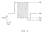
- the method is characterized in that when the intensity of the light beams is represented by power level P 1 that can melt an irradiated portion instantly, power levels P 2 and P 3 (where P 1 > P 2 ⁇ P 3 ⁇ 0) that cannot melt an irradiated portion instantly, and power level P 0 (where P 1 > P 0 > 0) that does not change an optical state of a recording mark and provides reflected beams sufficient to reproduce the recording mark by irradiation, at least one recording mark to be recorded in the recording layer is formed with a recording pulse train consisting of a group of pulses generated by modulating the light beams between the power levels P 1 and P 3 .
- the recording mark is not to be recorded, the light beams are maintained at the power level P 2 , and information recorded in the recording layer is reproduced by irradiating the light beams at the power level P 0 .
- the above-described production methods can be applied to an optical information recording medium including two or more information layers.
- the light beams are incident from the side of the transparent substrate, and the state of the recording layers included in the first information layer and the second information layer can be changed.
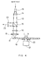
- An apparatus for recording and reproducing an optical information recording medium of the present invention includes an optical information recording medium of the present invention, a light beam generator for generating light beams with which the optical information recording medium is irradiated, and a light beam intensity modulator for modulating the intensity of the light beams.
- the intensity of the light beam is represented by power level P 1 that can melt an irradiated portion instantly, power levels P 2 and P 3 (where P 1 > P 2 ⁇ P 3 ⁇ 0) that cannot melt an irradiated portion instantly, and power level P 0 (where P 1 > P 0 > 0) that does not change an optical state of a recording mark and provides reflected beams sufficient to reproduce the recording mark by irradiation, in the case where information is recorded by forming a recording mark in the recording layer, the light beam intensity modulator modulates the light beams between the power levels P 1 and P 3 , so as to generate a recording pulse train consisting of a group of pulses, thereby forming at least one recording mark.
- the light beam intensity modulator maintains the intensity of the light beams at the power level P 2 .
- the light beam intensity modulator maintains the intensity of the light beams at the power level P 0 .
- the above-described apparatuses can be applied to an optical information recording medium including two or more information layers.
- the light beam generator can be provided on the side of the transparent substrate so that laser light is incident from the side of the transparent substrate.
- the present invention can provide an optical information recording medium suitable for recording and reproducing information in high density and with a small level of cross erase. Furthermore, the present invention can provide an optical information recording medium that allows recording and reproducing of information with a high erasure ratio and small jitter in overwriting in high density and at high linear velocity. In addition, the present invention can provide a method for producing these optical information recording media, a method for recording and reproducing information on an optical information recording medium suitable for the media of the present invention, and an apparatus for recording and reproducing information on an optical information recording medium.
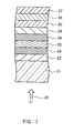
- Fig. 1 is a partial cross-sectional view of an embodiment of an optical information recording medium of the present invention.
- Fig. 2 is a partial perspective view of an embodiment of an optical information recording medium of the present invention.
- Fig. 3 is a partial cross-sectional view of another embodiment of an optical information recording medium of the present invention.
- Fig. 4 is a drawing showing the structure of an embodiment of an optical information recording/reproducing apparatus of the present invention.
- Fig. 5 is a waveform chart applied to a method for recording and reproducing information on the optical information recording medium of the present invention.
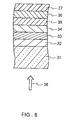
- Fig. 6 is a partial cross-sectional view of still another embodiment of an optical information recording medium of the present invention.
- Fig. 7 is a partial cross-sectional view of yet another embodiment of an optical information recording medium of the present invention.
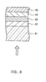
- Fig. 8 is a partial cross-sectional view of another embodiment of an optical information recording medium of the present invention.
- a first optical information recording medium of the present invention will be mainly described.
- the cross erase is influenced significantly by the relationship between the thickness of a recording layer and the heat conductivity of layers closer to the air side (the side opposite to the substrate) than the recording layer is, and achieved the medium of this embodiment.
- the thickness of an upper protective layer preferably is 10nm or more.
- the thickness of the upper protective layer preferably is 200nm or less.
- the optical information recording medium preferably further includes an interface layer formed in contact with the recording layer.
- the interface layer is formed at least either between the upper protective layer and the recording layer or between a lower protective layer and the recording layer. It is preferable that the interface layer comprises Ge to prevent mutual diffusion of atoms between the upper protective layer and/or the lower protective layer and the recording layer.
- the interface layer preferably comprises at least one selected from the group consisting of Ge, Si, Cr, Ti and Al.
- the recording layer comprises Ge, Sb and Te, because these materials are suitable for erasing and recording performed simultaneously in the recording layer. More preferably, the recording layer comprises Ge, Sb and Te as main components and further contains 6.0 at% or less of N to improve the repetition characteristics.
- the upper protective layer and/or the lower protective layer contain 60 to 100 mol% of ZnS and 40 to 0 mol% of SiO 2 .
- Such a protective layer has excellent heat resistance, an appropriate heat conductivity and a refractive index appropriate to adjust the optical characteristics of the medium.
- the reflective layer comprises at least one selected from the group consisting ofAu, Ag, Cu and Al. Alloys comprising these metals can be used.
- the intermediate layer comprises at least one element selected from the group consisting of Ti, Zr, Hf, V, Nb, Ta, Cr, Mo, W, Mn, Os, Al, Ga, In, C, Si, Ge, Sn, Pb, Sb and Bi. More specifically, it is preferable that the intermediate layer comprises at least one compound selected from the group consisting of oxide, nitride, carbide, sulfide, fluoride, selenide and telluride comprising at least one selected from the above-mentioned elements, or a compound consisting of at least two elements selected from the above described elements such as Ge-Cr and Si-W.
- the intermediate layer is formed of a material having a heat conductivity between the heat conductivity of the upper protective layer and the heat conductivity of the reflective layer.
- the reflectance difference (Rcry-Ramo) is 5% or more (5 points or more in representation by %), and the absorptance ratio (Acry/Aamo) is 1.0 or more, where Rcry and Acry are a reflectance that is a ratio of light beams reflected by the recording medium and an absorptance that is a ratio of light beams absorbed by the recording layer, respectively, when the recording layer is crystalline, and Ramo and Aamo are those when the recording layer is amorphous.
- This preferable example solves the problem of non-uniformity of the mark edge positions at the time of overwriting.
- the recording layer is formed at a rate of 200nm/min or less in order to ensure the precision in the thickness of the recording layer.
- the recording layer in an atmosphere containing inert gas and nitrogen gas, where the content of the nitrogen gas is adjusted so that the recording layer contains 6.0at% or less of nitrogen atoms.
- At least a part of a recording pulse train is generated so that the pulse widths and the pulse intervals are substantially identical to other widths and intervals.
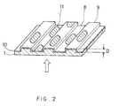
- Figs. 1 and 2 are a partial cross-sectional view and a partial perspective view of an optical disk of this embodiment.
- this optical disk includes a transparent disk substrate 1, a lower protective layer 2, a recording layer 3, an upper protective layer 4, an intermediate layer 5 and a reflective layer 6. These layers are laminated sequentially on the transparent disk substrate 1.
- an overcoat layer 7 is provided thereon.
- grooves 8 having a depth D are formed on the substrate 1, concave portions and convex portions, which extend in parallel to each other, are formed on the surface of a multi-layered film 10 including the above-described layers as the grooves 8 and lands 9.
- the recording layer 3 is irradiated with laser light as light beams from the side of the substrate 1, so as to form a recording mark 11. As shown in Fig. 2, it is preferable to form the recording marks both on the groove 8 and the land 9 to achieve high density recording (land and groove recording).
- the substrate 1 can be formed of a material such as a polycarbonate resin, a polymethylmethacrylate resin, a polyolefin resin, an Arton resin, glass or the like.
- the thickness of the substrate 1 is not limited to a particular thickness, but a thickness of 0.1 to 2.0mm is preferable.
- the lower protective layer 2 and the upper protective layer 4 are formed to prevent increase of noise due to thermal damage to the substrate 1 or the recording layer 3 during irradiation of laser light, and to adjust the reflectance and the absorptance with respect to the laser light and the phase of reflected light.
- the protective layers 2 and 4 can be formed of a dielectric material such as an oxide of Sc, Y, Ce, La, Ti, Zr, Hf, V, Nb, Ta, Zn, Al, Si, Te or the like, a nitride of Ti, Zr, Hf, V, Nb, Ta, Cr, Mo, W, Zn, B, Al, Ga, In, Si, Ge, Sn, Pb or the like, a carbide of Ti, Zr, Hf, V, Nb, Ta, Cr, Mo, W, Zn, B, Al, Ga, In, Si or the like, a sulfide of Zn, Cd, Ga, In, Si, Ge, Sn, Pb, Sb, Bi or the like, a selenide or a telluride, a fluoride of Mg, Ca or the like, a single-element substance such as C, Si, Ge or the like, or a mixture of these.
- a dielectric material such as an oxide of Sc, Y
- the thickness of the upper protective layer 4 preferably is 10nm to 200nm.
- the thickness of the upper protective layer 4 is too small, heat hardly escapes from the recording layer 3 to the intermediate layer 5 due to the heat that the intermediate layer 5 itself has, as described above.
- the heat conductivity in the direction of the thickness of the layers drops, the heat diffusion in the plane of the recording layer 3 becomes large, thus leading to a possibility that the cross erase may increase.
- the upper protective layer 4 is 10nm or more, the cross erase can be in an acceptable range, even if, for example, the track pitch (which is the average of the width of a pair of adjacent land and groove (1/2 of a groove pitch), or is equal to a groove pitch when recording is performed only in grooves) is 0.6 ⁇ m.
- the thickness thereof preferably is 200nm or less, although this may depend on the wavelength ⁇ and the refractive index n.
- the thickness of the upper layer 4 preferably is from 10nm to 200nm, and more preferably 20nm to 200nm.
- the thickness of the lower protective layer 2 is not limited to a particular value, but preferably is 10nm to 200nm.
- the thickness of the lower protective layer is less than 10nm, the substrate may be deformed by heat.
- the reason why a thickness of the lower protective layer of 200nm or less is preferable is the same as the reason why a thickness of the upper protective layer of 200nm or less is preferable.
- the recording layer 3 can be formed of an alloy comprising chalcogenide, a material based on Te or Se, such as Ge-Sb-Te, Ge-Te, Pd-Ge-Sb-Te, In-Sb-Te, Sb-Te, Ag-In-Sb-Te, Ge-Sb-Bi-Te, Ge-Sb-Se-Te, Ge-Sn-Te, Ge-Sn-Te-Au, Ge-Sb-Te-Cr, In-Se, In-Se-Co or the like, as a main component.
- a material where oxygen, nitrogen or the like is added to these alloys can be used.
- the thickness of the recording layer 3 preferably is 4nm to 16nm.
- a thickness of 20nm or more was advantageous to achieve a large optical contrast.
- such a thick recording layer leads to large heat conduction in the in-plane direction of the recording layer. Therefore, as the track pitch becomes smaller (e.g., 0.6 ⁇ m or less), the cross erase becomes more significant.
- a thin recording layer is advantageous in order to reduce the cross erase. Making a thin recording layer allows the heat conduction in the in-plane direction of the layer to be reduced.
- the thickness of the recording layer when the thickness of the recording layer is 16nm or less, the cross erase can be within an acceptable range even if the track pitch is 0.6 ⁇ m.
- the thickness of the recording layer when the thickness of the recording layer is less than 4nm, not only can the optical contrast not be obtained, but also the influence of thickness variation due to repetitive recording becomes large, so that tracking becomes unstable, leading to large cross erase. Therefore, the thickness of the recording layer preferably is 4nm to 16nm, more preferably 6nm to 14nm.
- the intermediate layer 5 preferably is formed of a material comprising at least one element selected from the group consisting of Ti, Zr, Hf, V, Nb, Ta, Cr, Mo, W, Mn, Re, Fe, Ru, Os, Al, Ga, In, C, Si, Ge, Sn, Pb, Sb, and Bi, or a material comprising at least one compound selected from the group consisting of oxide, nitride, carbide, sulfide, fluoride, selenide and telluride of at least one selected from the above-mentioned elements.
- the thickness of the intermediate layer 5 is not limited to a particular value, but a thickness of 5nm to 100nm is preferable.
- the reflective layer 6 is formed to adjust the reflectance and the absorptance with respect to laser light, and the phase of reflected light, reduce the thermal load in the recording thin film, or the like.
- the reflective layer can be formed of a metal material having a relatively high heat conductivity such as Al, Au, Ag, Cu or the like, or an alloy material based on these metal materials.
- the thickness of the reflective layer 6 is not limited to a particular value, but a thickness of 10nm to 200nm is preferable.
- a suitable material used for each layer can be selected individually from the examples listed above.
- the intermediate layer 5 and the upper protective layer 4 materials thereof are selected so that the heat conductivity of the reflective layer 6 is larger than that of the intermediate layer 5, and the heat conductivity of the intermediate layer 5 is larger than that of the upper protective layer 4.
- the heat conductivity is set in such a manner, the heat conduction is accelerated from the recording layer 3 in the thickness direction of the multi-layered film. Therefore, the heat conduction in the in-plane direction of the recording layer 3 can be suppressed relatively, so that the influence on adjacent tracks can be small.
- an interface layer 12 can be provided in the optical information recording medium.
- the interface layer 12 can be provided on both sides of the recording layer 3, as shown in Fig. 3. Alternatively, the interface layer 12 can be provided on either one of the sides.
- the interface layer 12 can suppress atomic diffusion between the protective layers 2 and 4 and the recording layer 3, so that the repetition characteristics of the recording medium can improve.
- the interface layer 12 can be formed of a material having a diffusion preventing effect with respect to the materials for the protective layers 2 and 4.
- a material comprising Ge is preferable, and a material comprising a nitride of Ge as a main component is most preferable.
- the thickness of the interface layer 12 is not limited to a particular value, but a thickness of 1nm to 50nm is preferable.
- the layers 2 to 6, and 12 can be formed by a vapor thin film deposition method such as a vacuum evaporation method, sputtering, ion plating, a CVD (chemical vapor deposition) method, an MBE (molecular beam epitaxy) method or the like.
- a vapor thin film deposition method such as a vacuum evaporation method, sputtering, ion plating, a CVD (chemical vapor deposition) method, an MBE (molecular beam epitaxy) method or the like.
- sputtering is most preferable when the advantages and the disadvantages in the film formation rate, the production cost and the quality of the obtained film are balanced.
- Each layer generally is formed while allowing inert gas to flow in a chamber under high vacuum.
- the layer can be formed while mixing oxygen, nitrogen or the like with the inert gas.
- oxygen atoms or nitrogen atoms are contained in the film so that the characteristics of the film can be adjusted.
- the optical information recording medium it is industrially advantageous to form the layers 2 to 6 and 12 in separate chambers in parallel and sequentially by a single wafer processing film-forming apparatus.
- this film-forming method even if the recording layer is formed at a relatively low rate, that does not affect the efficiency of the whole formation of the films.
- the thickness of the recording layer 3 is 4nm to 16nm and it is, for example, about one order of magnitude smaller than a normal thickness (100nm or more) of the lower protective layer 2. Since it is important to control the thickness of the recording layer 3 precisely in order to reduce the cross erase, as described above, it is preferable to take at least about 5 seconds to form the recording layer.
- a film-forming rate for the recording layer of 200nm/min. or less is preferable.
- An overcoat layer 7 may be provided on the thus formed layers, as shown in Fig. 1.
- the layer 7 preferably is formed by coating an ultraviolet curable resin.
- the optical information recording medium is not limited to the single plate one-sided disk as shown in Fig. 1, and can be a two-sided disk formed by attaching substrates on which multi-layered films including the recording layers are formed as described above so that the surfaces of the films are facing each other with an ultraviolet curable resin and/or a hotmelt type adhesive.
- the present invention can be a one-sided disk by attaching a dummy substrate onto the surface on which the multi-layered film is formed via the adhesive as described above.
- Fig. 4 is a schematic view of an example of an apparatus for recording and reproducing information on the optical information recording medium of the present invention.
- Laser light 10 emitted from a semiconductor laser 13 in accordance with an input signal is collimated by collimate lens 14 into parallel beams, and then passes through a beam splitter 15, a quarter-wave plate 16, and an object lens 17 sequentially, and then an optical disk 18 is irradiated with the light beams.
- the laser light 10 is focused by moving a voice coil 19 upward or downward.
- the optical disk 18 is secured onto a turn table 20.
- Information signals are recorded and reproduced by irradiating the optical disk 18 that is rotated at a predetermined rate by a motor 21 with the laser light.
- Fig. 5 is an example of a pulse waveform of the laser light for recording of information signals.
- the intensity of the laser light is modulated among P 1 , P 2 , P 3 and P 4 .
- P 1 is a power level that allows the irradiated portion to be melted instantly, and preferably, a power level that allows the irradiated portion to be melted instantly even if the portion is irradiated while modulating the intensity at power levels equal to or less than this power level, as shown in Fig. 5.
- P 2 and P 3 are power levels that do not allow the irradiated portion to be melted instantly, and preferably that do not allow the irradiated portion to be melted instantly even if the portion is irradiated without modulating the intensity.
- P 4 is a power level for cooling the recording layer immediately after the last recording pulse train.
- Fig. 5 shows an example where the power levels are set so that P 1 > P 2 ⁇ P 1 ⁇ P 4 ⁇ 0.
- the intensity of the laser beam can be modulated in the manner described above by modulating the driving current of a semiconductor laser.
- an electro-optical modulator, an acousto-optical modulator or the like can be used.
- a pulse train for a short mark length can be formed with a single rectangular pulse of power level P 1 .
- P 2 is a power level at which a recording mark cannot be formed even if light beam is maintained at this intensity for irradiation, as shown in Fig. 5.
- a power level that cannot form a recording mark but can erase a recording mark can be set as the power level P 2 . In this case, a recording mark in a portion irradiated with light beams at the power level P 2 is erased.
- a power level that can change the recording layer reversibly from the crystalline state to the amorphous state can be set as P 1
- a power level that can change the recording layer reversibly from the amorphous state to the crystalline state can be set as P 2 .
- a cooling section at power level P 4 is provided immediately after the recording pulse train as shown in Fig. 5.
- the power level for cooling is provided, heat can be removed in a mark rear end portion, which especially tends to have excessive heat, thus suppressing the cross erase.
- modulation can be performed with a signal frequency so that modulation means can be simplified.
- mark edge positions may be non-uniform for each pattern of the length of a recording mark, the length of a space before and after the recording mark, and the length of an adjacent mark, thus causing an increase of jitter.
- Information signals recorded in this manner are reproduced by irradiating the optical disk with laser light (non-modulated light) of power level P 0 at which the recording layer 3 is not phase changed, and allowing reflected light thereof to be incident to a detector 22 and detecting a change in the amount of the reflected light as a reproduction signal 23.
- the power level of the laser light can be changed, as described above, by controlling the driving current of the laser diode.
- an electro-optical modulator, an acousto-optical modulator or the like can be used as the light beam intensity modulating means.
- the optical information recording medium it is preferable to provide an interface layer at least at one interface between a lower protective layer and a recording layer and between a recording layer and an upper protective layer.
- This preferable example improves the erasing characteristics.
- the interface layer comprises at least one selected from the group consisting of Ge, Si, Cr, Ti and Al.
- the thickness of the recording layer preferably is 4nm to 16nm.
- the optical contrast or the signal amplitude becomes small.
- it is too thick the heat diffusion in the direction of the in-plane of the recording layer becomes large, thus resulting in large thermal interference between marks.
- the thickness of the upper protective layer preferably is 10nm to 200nm.
- the upper protective layer is excessively thin, heat generation due to light absorption of a light absorption layer affects the recording layer, thus resulting in large thermal interference between marks.
- a cooling effect by a reflective layer becomes small, thus resulting in imbalance between the front end and the rear end of a mark.
- the thickness of the lower protective layer 2 is not limited to a particular value, but preferably is 10nm to 200nm.
- the recording layer preferably comprises Ge, Sb and Te, and more preferably comprises Ge, Sb and Te as main components and further comprises 6.0at% of N.
- the upper protective layer and/or the lower protective layer preferably comprises 60 to 100 mol% of ZnS and 40 to 0 mol% of SiO 2 .
- the reflective layer preferably comprises at least one selected from the group consisting ofAu, Ag and Cu.
- the light absorption layer comprises at least one element selected from the group consisting of Ti, Zr, Hf, V, Nb, Ta, Cr, Mo, W, Mn, Os, Al, Ga, In, C, Si, Ge, Sn, Pb, Sb and Bi. More specifically, it is preferable that the light absorption layer comprises at least one compound selected from the group consisting of oxide, nitride, carbide, sulfide, fluoride, selenide and telluride comprising at least one selected from the above-mentioned elements, or a compound consisting of at least two elements selected from the above described elements.
- the reflectance difference (Rcry-Ramo) is 5% or more (5 points or more in representation by %), and the absorptance ratio (Acry/Aamo) is 1.0 or more, where Rcry and Acry are a reflectance that is a ratio of light beams reflected by the recording medium and an absorptance that is a ratio of light beams absorbed by the recording layer, respectively, when the recording layer is crystalline, and Ramo and Aamo are those when the recording layer is amorphous.
- This preferable example solves the problem of non-uniformity of the mark edge positions at the time of overwriting.
- the recording layer is formed at a rate of 200nm/min or less in order to ensure the precision in the thickness of the recording layer.
- the recording layer in an atmosphere containing inert gas and nitrogen gas, where the content of the nitrogen gas is adjusted so that the recording layer contains 6.0at% or less of nitrogen atoms.
- At least a part of a recording pulse train is generated so that the pulse widths and the pulse intervals are substantially identical to other widths and other intervals.
- Fig. 6 is a partial cross-sectional view of an optical information recording medium of this embodiment.
- Fig. 7 is a partial cross-sectional view of another example of an optical information recording medium of this embodiment.
- a lower protective layer 32, a recording layer 33, an upper protective layer 34, a light absorption layer 35 and a reflective layer 36 are laminated sequentially on a substrate 31. Further, an overcoat layer 37 is provided on the reflective layer 36. This disk is irradiated with laser beam 38 from the side of the substrate 31 for recording and reproduction of the disk.
- the substrate 31, the lower protective layer 32, the recording layer 33 and the upper protective layer 34 can be formed of the materials described with reference to the first embodiment.
- the light absorption layer 35 is formed in order to adjust the reflectance and the absorptance with respect to the laser light 38 and the phase of reflected light, or the like. It is preferable that the light absorption layer comprises at least one selected from the group consisting of Ti, Zr, Hf, V, Nb, Ta, Cr, Mo, W, Mn, Re, Fe, Ru, Os, Al, Ga, In, C, Si, Ge, Sn, Pb, Sb and Bi, or a material comprising at least one compound selected from the group consisting of oxide, nitride, carbide, sulfide, fluoride, selenide and telluride comprising at least one selected from the above-mentioned elements.
- the reflective layer 36 is formed to adjust the reflectance and the absorptance with respect to the laser beam 38 and the phase of reflected light, reduce the thermal load in the recording thin film, or the like.
- the reflective layer preferably is formed of a metal material having a relatively high heat conductivity such as Al, Au, Ag, Cu or the like, especially Au, Ag, Cu, which have a refractive index of less than 0.5 at a wavelength in the 600nm range, or an alloy material based on these metal materials.
- an Ag alloy is excellent in the heat conductivity and the optical constant, and is less expensive than Au having equal characteristics.
- a material containing 10at% or less of Pd, Cu, Ti or the like in addition to Ag hardly is corroded, and is preferable in view of environmental resistance and reliability.
- the materials used for the lower protective layer 32 and the upper protective layer 34 there are some dielectric materials that function as the interface layer 39.
- the interface layer 39 can be formed of one of those materials, but especially a material comprising a nitride of Ge as a main component is most preferable. Furthermore, such an interface layer 39 can improve the erasing characteristics.
- the protective layer 32, the recording layer 33, the upper protective layer 34, the light absorption layer 35, the reflective layer 36 and the interface layer 39 can be formed in the same manner as in the first embodiment.
- the optical information recording medium can be a single plane one-sided disk by being overcoated with a ultraviolet curable resin. Furthermore, the optical information recording medium of this embodiment can be used as a two-sided disk, as described in the first embodiment. In addition, the optical information recording medium of this embodiment can be used as a one-sided disk by attaching a dummy substrate to the surface of the film so that they are opposed to each other.
- the optical information recording medium of this embodiment is characterized by a combination of the materials and the thicknesses of the light absorption layer 35 (having a refractive index n 1 , an extinction coefficient k 1 , and an thickness d 1 ) and the reflective layer 36 (having a refractive index n 2 , an extinction coefficient k 2 , and an thickness d 2 ).
- the function and the effect of each layer will be described.
- both Acry/Aamo and ⁇ R can be large.
- the above-described ranges can be supported by the following optical calculation:
- the refractive index, the extinction coefficient and the thickness of each layer of the multi-layered film are determined.
- an equation for light energy at each interface is formulated based on the law of the conservation of energy, and the simultaneous equations for all the interfaces are solved, so that the reflectance and the transmissivity of the entire multi-layered film and the absorptance of each layer can be calculated.
- This approach is well-known, for example, as a matrix method (e.g., "Wave Optics" by Hiroshi Kubota et al., Iwanami Shoten, 1971).
- Acry/Aamo and ⁇ R were calculated with respect to a multi-layered structure medium including the substrate 31 / the lower protective layer 32 (an arbitrary thickness) / the recording layer 33 (10nm) / the upper protective layer 34 (arbitrary thickness) / the light absorption layer 35 (thickness d 1 ) / the reflective layer 36 (80nm) from the side to which laser beam (a wavelength of 660nm) is incident.
- ⁇ n n 1 -n 2 preferably is at least two, and more preferably at least three.
- a preferable range of the thickness d 1 of the light absorption layer 35 is 0,1 ⁇ /(n 1 . k 1 ) ⁇ d 1 ⁇ 1.0 ⁇ /(n 1 . k 1 ), where ⁇ is a wavelength of incident light, and more preferably 0.2 ⁇ /(n 1 . k 1 ) ⁇ d 1 ⁇ 0.8 ⁇ /(n 1 . k 1 ).
- the reflective layer 36 In order to obtain a cooling ability, a material having a large heat conductivity is used for the reflective layer 36, so that the mark widths are uniform to reduce jitter.
- the heat conductivity of the reflective layer preferably is, for example, 50W/m ⁇ K or more under temperature conditions in the vicinity of 300K, more preferably 100W/m•K or more, and most preferably 150W/m•K or more.
- the thickness d 2 of the reflective layer 36 preferably is equal to or more than the thickness d 1 of the light absorption layer 35, more preferably 1.5 times the thickness d 1 or more, and most preferably twice the thickness d 1 or more.
- the method for producing the optical information recording medium, the method for recording and reproducing information thereon, and the apparatus for recording and reproducing information thereon in this embodiment are the same as those in the first embodiment.
- the thickness of the recording layer was 10nm, but the present invention is not limited thereto.
- an optical information recording medium comprising at least two multi-layered films including a recording layer
- two layers of multi-layered films are formed via a separating layer.
- a first information layer 42, a separating layer 43, a second information layer 44, and a protective layer 45 are formed on a transparent substrate 41 in this order.
- Each of the first information layer 42 and the second information layer 44 includes a recording layer.
- the recording layers are irradiated with laser light from the side of the transparent substrate so that information is recorded and reproduced.
- the multi-layered film as described in the above embodiments can be applied.
- the first information layer 42 it is preferable to use a multi-layered film including a recording layer, a lower protective layer and an upper protective layer provided on both sides of the recording layer.
- Each layer and a transparent substrate included in these multi-layered films can be formed of the materials as described in the above embodiments.
- the first information layer may be a read-only layer for reproducing information that already has been stored as concave-convex patterns on the surface of a transparent substrate.
- the first information layer 42 transmits at least 30% of laser light irradiated because information is recorded and reproduced in the second information layer 44.
- the separating layer 43 it is preferable to use a material that is transparent at a wavelength ⁇ of laser light and has excellent heat resistance and adhesion. More specifically, an adhesive resin (e.g., ultraviolet curable resin), a double-sided adhesive tape, and other various dielectric films can be used.
- the thickness of the separating layer 43 preferably is not less than 2 ⁇ m so that at the time of recording or reproducing information on either one of the first information layer 42 or the second information layer 44, information in the other information layer does not leak thereto.
- the thickness of the separating layer 43 preferably is not more than 100 ⁇ m so that the total thickness of the separating layer and the substrate is in a substrate thickness tolerance zone in order to focus the laser light on both of the first information layer 42 and the second information layer 44.
- the protective layer 45 can be utilized as a substrate (protective substrate) on which the second information layer 44 is formed.
- the transparent substrate 41 on which the first information layer 42 is formed and the protective substrate on which the second information layer 44 is formed are attached via the separating layer 43 to produce an optical disk.
- the same material as that of the transparent substrate 41 can be used as the material of the protective substrate, it is not necessary to be transparent, and other materials can be used.
- the shape of the surface of the substrate it is not necessary to use the same shape as that of the surface of the transparent substrate.
- the shape of the guide grooves consisting of grooves and lands can be different, or the spiral direction of the guide grooves can be opposite.
- the surface of the protective substrate may be smooth.
- the protective layer 45 may be formed on the second information layer 44 formed on a transparent substrate.
- Such a protective layer can be formed by attaching a resin sheet, for example by spin coating or with an adhesive.
- the first information layer and the second information layer are formed on the surfaces of the transparent substrate and the protective substrate on each of which guide grooves are formed by sputtering or the like, as described above. Then, an ultraviolet curable resin is applied onto the surface of the first information layer and the second information layer so as to form the separating layer. Furthermore, the transparent and the protective substrate are pressed so that the first information layer and the second information layer are opposed to each other via the separating layer, and irradiated with ultraviolet rays so as to cure the separating layer.
- a polycarbonate resin having a thickness of 0.6mm was used as a substrate. Lands and grooves, each of which has a width of 0.6 ⁇ m, were formed on the substrate. The depth of the groove was about 70nm.
- These layers were formed by sputtering and laminated one after another.
- the sputtering targets for all the layers had a diameter of 10cm and a thickness of 6mm.
- All the layers except the recording layer were formed in an Ar gas, and the recording layer was formed in a mixed gas of Ar and N 2 (a total pressure of 2mTorr and a partial pressure of N 2 gas of about 5%).
- optical disks Nos. 1 to 21 were produced. These optical disks were produced by intentionally changing the thicknesses of the recording layer and the upper protective layer and the materials of the intermediate layer and the reflective layer in order to investigate the dependence of cross erase on the material and the thickness structure.
- Table 2 shows the thicknesses of the recording layer and the upper protective layer and the materials of the intermediate layer and the reflective layer of each optical disk.
- Mark edge recording was performed at a linear velocity of 6.0m/s (the radius position is at about 32mm and the rotation number is about 1800rpm) on these optical disks using an optical system with a wavelength of 660 nm and an NA of 0.6, and cross erase was measured.
- a 3T signal with 9.7MHz was recorded on a groove, and this track was reproduced so as to measure an amplitude A 0 of the 3T signal with a spectrum analyzer.
- an 11T signal with 2.6MHz was recorded on lands adjacent to the groove on both sides, and the groove was reproduced again so as to measure an amplitude A 1 of the 3T signal with the spectrum analyzer.
- the thus measured drop amount ⁇ A A 1 -A 0 of the amplitude of the 3T signal was used as the index for cross erase evaluation.
- the same operations were performed except that the land and the groove are used in the other way around, and the drop amount ⁇ A' of the amplitude of the 3T signal was measured.
- Table 2 shows the evaluation grade based on the value of ⁇ A of each disk.
- the results of the measurement above showed that for all the samples, the drop amount of the amplitude of the 3T signal was larger when the groove was used as the track to be measured ( ⁇ A > ⁇ A'). Therefore, the evaluation was based on only the results ( ⁇ A) of that case.
- the sample having a value of ⁇ A of less than 1dB is shown by "A”
- the sample having a value of ⁇ A of 1dB or more and less than 2dB is shown by "B”
- the sample having a value of ⁇ A of 2dB or more and less than 5dB is shown by "C”
- the sample having a value of ⁇ A of 5dB or more is shown by "D”.
- a single rectangular pulse with a pulse width of 51.3ns (powder level P 1 ) was used for the 3T signal.
- a pulse train consisting of 9 pulses (powder level P 1 ) was used.
- the pulse width of the leading pulse in the pulse train was 51.3ns
- the pulse width of all the pulses other than the leading pulse was 17.1ns
- the width between the pulses was 17.1ns (powder level P 3 ).
- a cooling section of 34.2ns (powder level P 4 ) was provided immediately after the last pulse. For a portion where no mark is to be recorded, continuous light (non-modulated light) at power level P 2 was used.
- the recording power level P 1 was 1.5 times the lower limit of powers that allow the C/N ratio of the recorded 3T signal to exceed 45dB.
- the power level P 2 was the median in the range of powers that allow the erasure ratio, which is a damping ratio in the amplitude of the 3T signal when the 11T signal is overwritten on the recorded 3T signal, to exceed 25dB.
- the power levels P 3 and P 4 were 1mW, which was equal to the reproducing power level. No.
- recording layer upper protective layer intermediate layer material reflective layer material ⁇ A 1 4nm 15nm Cr Al C 2 8nm 15nm Cr Al A 3 12nm 15nm Cr Al B 4 16nm 15nm Cr Al C 5 20nm 15nm Cr Al D 6 12nm 3nm Cr Al D 7 12nm 6nm Cr Al D 8 12nm 9nm Cr Al C 9 12nm 12nm Cr Al B 10 12nm 18nm Cr Al B 11 12nm 21nm Cr Al A 12 12nm 15nm PbTe Al A 13 12nm 15nm WSi 2 Al A 14 12nm 15nm Ti Al B 15 12nm 15nm Cr WSi 2 D 16 12nm 15nm Cr Ti D 17 12nm 15nm Al Cr D 18 12nm 15nm Al ZnS-SiO 2 D 19 12nm 15nm Cr ZnS-SiO 2 D 20 12nm 15nm absent Al D 21 12nm 15nm Cr absent D
- the heat conductivity of each material used for the intermediate layer and the reflective layer depends on the temperature, approximate value ranges can be specified as follows: in the order of the largest heat conductivity, the heat conductivity of Al is about 150 to 250W/m•k at 30 to 600°C; 50 to 100W/m•k for Cr; 20 to 50W/m•k for Ti; 5 to 20W/m•k for WSi 2 ; 1.0 to 3.0W/m•k for PbTe; and 0.1 to 0.5W/m•k for ZnS-SiO 2 .
- the thickness of the recording layer is required to be from 4nm to 16nm, preferably from 6nm to 14nm, in view of the reduction of the cross erase.
- the thickness of the upper protective layer preferably is 10nm or more, and more preferably 20nm or more, in view of the reduction of the cross erase.
- optical disks No. 3 and Nos. 12 to 21, where the materials of the intermediate layer and the reflective layer are different are compared. Among them, apart from No.3, the cross erase in Nos. 12 to 14 is small.
- Al which has the largest heat conductivity among the materials used in this example was used for the reflective layer, and the materials for the intermediate layers have a heat conductivity between that of the upper protective layers and that of the reflective layers.
- the cross erase can be suppressed by selecting materials for the layers so that the layers have heat conductivities that vary from low to high gradually from layer to layer in the order of the closeness to the recording layer. This is because in the process of transmitting heat from the recording layer to the reflective layer via the upper protective layer and the intermediate layer, the transmitting rate is accelerated so that the heat conductivity in the plane of the recording layer is reduced, thereby suppressing the influence on the adjacent tracks.
- the GeON film was formed with a Ge target in a gas containing Ar, N 2 and O 2 by reactive sputtering.
- 3T signals and 11T signals were recorded alternately 10,000 or 100,000 times, and a change of the amplitude of the 3T signal from the amplitude of a 3T signal after 10 recordings was measured.
- compositions of the recording layers of the optical disks were analyzed by an Auger electron spectroscopy. The results were that the ratio of N atoms was about 2.2 at%. Furthermore, a plurality of optical disks with the same structure as that of No.3 were formed by changing the partial pressure of the N 2 gas during the formation of the recording layer. As a result of analysis, the ratios of N atoms in the recording layers were about 0.0, 0.2, 0.8, 4.0 and 7.6 at%.
- 3T signals and 11T signals were recorded alternately 10,000 or 100,000 times, and a change of the amplitude of the 3T signal from the amplitude of the 3T signal after 10 recordings was measured.
- the results were as follows. After 10,000 recordings, the amplitude drop in all of the optical disks was 0.5dB or less, which is in an error range. However, after 100,000 recordings, the amplitude of only the disk having a ratio of N atoms in the recording layer of 0.0 at% dropped by about 2dB, whereas the amplitude of the optical disk having a ratio of N atoms of about 0.2 at% dropped by 1dB, and the amplitude of other disks dropped by 0.5dB or less, which is within an error range. Furthermore, a 3T signal was recorded on these disks, and the amplitude of the 3T signal was measured.
- the disks were stored under an environment at 90°C and a relative humidity of 80% for 100 hours, and then the amplitude of the 3T signal was measured so as to obtain a change in the amplitude.
- the results were that the amplitude of the disk having a ratio of N atoms in the recording layer of 7.6 at% dropped by 5dB or more, the amplitude of the disk having a ratio of 4.0 at% dropped by about 2dB, and the amplitude of the other disks did not substantially drop.
- a preferable ratio of N atoms in the recording layer is 0.0 to 6.0 at% and more preferably 0.5 to 4.0 at%.
- the depth of the groove was about 70nm.
- Reflective layers with various thicknesses were formed with various materials, for example, an Au target thereon. These layers were formed by sputtering and laminated one after another. The sputtering targets for all the layers had a diameter of 10cm and a thickness of 6mm. All the layers except the recording layer were formed by sputtering in an Ar gas, and the recording layer was formed in a mixed gas ofAr and N 2 (a total pressure of lmTorr and a partial pressure of N 2 gas of about 5%).
- optical disks Nos. 31 to 47 were produced. These optical disks were produced by intentionally changing the materials and the thicknesses of the light absorption layer and the reflective layer in order to investigate the dependence of the recording and reproducing characteristics on the material and the thickness structure. Table 3 shows the materials and the thicknesses of the light absorption layer and the reflective layer of each optical disk.
- Mark edge recording was performed at a linear velocity of 6.0m/s (the radius position is at about 32mm and the rotation number is about 1800rpm) on these optical disks using an optical system with a wavelength of 660 nm and an NA of 0.6, and the following measurement was performed.
- a 3T signal with 9.7MHz and a 11T signal with 2.6MHz were recorded on a groove and a land alternately 11 times, and this track where the 3T signal is recorded was reproduced so that the C/N ratio and the erasure ratio were measured with a spectrum analyzer.
- the erasure ratio is defined as a difference (A 3 -A 11 ) between the amplitude A 3 of the 3T signal and the amplitude A 11 of a 11T residual signal.
- jitter refers to a dislocation on the time axis between a recorded original signal and a reproduction signal, and is expressed as ( ⁇ sum/T) obtained by dividing a sum ( ⁇ sum) of standard deviations of jitters of signals of 3T to 11T by a window width (T) for signal detection.
- T window width
- nT (n is an integer, 3 ⁇ n ⁇ 1) signal
- a pulse train consisting of (n-2) pulses (powder level P 1 ) was used.
- the pulse width of the leading pulse in the pulse train was 51.3ns
- the pulse width of all the pulses other than the leading pulse was 17.1ns
- the width between the pulses was 17.1ns (powder level P3).
- a cooling section of 34.2ns (powder level P 4 ) was provided immediately after the last pulse. For a portion where no mark is to be recorded, continuous light (non-modulated light) at power level P 2 was used.
- the recording power level P 1 was 1.5 times the lower limit of powers that allow the C/N ratio to exceed 45dB when the 3T signal is recorded.
- the power level P 2 was a power that provides the largest erasure ratio.
- the power levels P 3 and P 4 were 1mW, which was equal to the reproducing power level.
- Table 3 shows the results of the measurement under the conditions described above.
- the sample that is sufficient for a practical recording medium is shown by “B”
- the sample that is particularly excellent is shown by “A”
- the sample that is insufficient but possibly usable depending on the specification of the density, linear velocity and the recording and reproducing system is shown by “C”
- the sample that cannot be used is shown by “D”. More specifically, as for the C/N ratio, "A” corresponds to 53dB ore more, “B” corresponds to 50dB or more and less than 53dB, “C” corresponds to 47dB or more and less than 50dB, and “D” corresponds to less than 47dB.
- A corresponds to 24dB or more
- B corresponds to 20dB or more and less than 24dB
- C corresponds to 16dB or more and less than 20dB
- D corresponds to less than 16dB.
- A corresponds to less than 8%
- B corresponds to 8% or more and less than 10%
- C corresponds to 10% or more and less than 13%
- D corresponds to 13% or more.
- the jitter becomes better because the cooling ability is raised.
- the thickness of the reflective layer is in the vicinity of the thickness equal to or more than the thickness of the light absorption layer, the jitter is 10% or less.
- an appropriate thickness of the light absorption layer is in a range from 0.1 ⁇ /(n 1 . k 1 )to 1.0 ⁇ /(n 1 . k 1 ).
- the materials of the light absorption layer and the reflective layer were changed.
- ⁇ n is 2.5 or more, more preferably 3 or more.
- the GeON film was formed with a Ge target in a gas containing Ar, N 2 and O 2 by reactive sputtering.
- the same measurement as that for the disk No. 34 was performed with respect to these disks. The results were as follows. All of the disks had C/N ratios similar to that of the disk No. 34.
- the disk including the interface layer 39 (GeON film) only on the surface of the recording layer 33 on the side of the substrate 31
- the disk including the interface layers 39 on the surfaces of the recording layer 33 both on the side of the substrate 31 and the side opposite thereto the erasure ratios thereof improved from that of the disk No. 34 by about 2dB, about 4dB, and about 5dB, respectively, and the jitter values were 8% or less, which is satisfactory.
Landscapes
- Physics & Mathematics (AREA)
- Optics & Photonics (AREA)
- Chemical & Material Sciences (AREA)
- Inorganic Chemistry (AREA)
- Engineering & Computer Science (AREA)
- Manufacturing & Machinery (AREA)
- Optical Record Carriers And Manufacture Thereof (AREA)
- Optical Recording Or Reproduction (AREA)
- Thermal Transfer Or Thermal Recording In General (AREA)
Applications Claiming Priority (4)
| Application Number | Priority Date | Filing Date | Title |
|---|---|---|---|
| JP22192498 | 1998-08-05 | ||
| JP22192498 | 1998-08-05 | ||
| JP32989098 | 1998-11-19 | ||
| JP32989098 | 1998-11-19 |
Publications (3)
| Publication Number | Publication Date |
|---|---|
| EP0978831A2 true EP0978831A2 (fr) | 2000-02-09 |
| EP0978831A3 EP0978831A3 (fr) | 2002-02-06 |
| EP0978831B1 EP0978831B1 (fr) | 2007-10-10 |
Family
ID=26524582
Family Applications (1)
| Application Number | Title | Priority Date | Filing Date |
|---|---|---|---|
| EP19990306206 Expired - Lifetime EP0978831B1 (fr) | 1998-08-05 | 1999-08-05 | Support d'enregistrement d'informations optiques et procédé pour sa fabrication, procédé d'enregistrement et de reproduction d'informations sur celui-ci, et appareil d'enregistrement et de reproduction |
Country Status (4)
| Country | Link |
|---|---|
| US (1) | US6268034B1 (fr) |
| EP (1) | EP0978831B1 (fr) |
| CN (1) | CN1143289C (fr) |
| TW (1) | TW448443B (fr) |
Cited By (10)
| Publication number | Priority date | Publication date | Assignee | Title |
|---|---|---|---|---|
| EP1351229A2 (fr) * | 2002-03-19 | 2003-10-08 | Matsushita Electric Industrial Co., Ltd. | Milieu d' enregistrement d' information et procédé pour sa fabrication |
| EP1367577A1 (fr) * | 2002-05-31 | 2003-12-03 | TDK Corporation | Support d'enregistrement optique et méthode d'enregistrement en utilisant le même |
| EP1376562A2 (fr) * | 2002-06-28 | 2004-01-02 | Pioneer Corporation | Support de reproduction / d'enregistrement d'informations |
| EP1431969A1 (fr) * | 2001-09-26 | 2004-06-23 | TDK Corporation | Support d'enregistrement optique et systeme d'enregistrement associe |
| US6996055B2 (en) | 2002-04-30 | 2006-02-07 | Tdk Corporation | Optical recording medium and method for optically recording data in the same |
| WO2006021960A1 (fr) * | 2004-08-26 | 2006-03-02 | Doron Schlesinger | Dispositif mince de stockage de données et processus pour sa fabrication |
| US7141289B2 (en) | 2003-08-25 | 2006-11-28 | Tdk Corporation | Optical information recording medium |
| US7157128B2 (en) | 2003-07-23 | 2007-01-02 | Tdk Corporation | Optical information recording medium |
| US7321481B2 (en) | 2002-07-04 | 2008-01-22 | Tdk Corporation | Optical recording medium |
| US7781146B2 (en) | 2002-11-22 | 2010-08-24 | Tdk Corporation | Optical recording medium |
Families Citing this family (23)
| Publication number | Priority date | Publication date | Assignee | Title |
|---|---|---|---|---|
| US6821707B2 (en) * | 1996-03-11 | 2004-11-23 | Matsushita Electric Industrial Co., Ltd. | Optical information recording medium, producing method thereof and method of recording/erasing/reproducing information |
| EP1662493B1 (fr) * | 1999-05-19 | 2010-07-14 | Mitsubishi Kagaku Media Co., Ltd. | Enregistrement à vitesse angulaire constante |
| WO2001086648A1 (fr) * | 2000-04-25 | 2001-11-15 | Matsushita Electric Industrial Co., Ltd. | Procede de fabrication de substrat de disque, procede et dispositif de fabrication de disque optique |
| TW575873B (en) * | 2000-07-13 | 2004-02-11 | Matsushita Electric Ind Co Ltd | Information recording medium, method for producing the same, and recording/reproducing method using the same |
| JP2003034081A (ja) * | 2000-09-14 | 2003-02-04 | Ricoh Co Ltd | 相変化型光情報記録媒体 |
| US20040013069A1 (en) * | 2000-09-29 | 2004-01-22 | Mayumi Uno | Optical information recording medium and recording and method of reproducing the record |
| CN1194348C (zh) * | 2000-11-30 | 2005-03-23 | 日本胜利株式会社 | 光记录媒体 |
| JP3777111B2 (ja) * | 2001-07-12 | 2006-05-24 | 日立マクセル株式会社 | 情報記録媒体および製造方法 |
| US7241549B2 (en) * | 2001-09-18 | 2007-07-10 | Ricoh Company, Ltd. | Information recording medium |
| WO2004025640A1 (fr) * | 2002-09-13 | 2004-03-25 | Matsushita Electric Industrial Co., Ltd. | Support de stockage d'information et son procede de fabrication |
| CN1333399C (zh) * | 2002-10-02 | 2007-08-22 | 三菱化学媒体股份有限公司 | 光记录介质 |
| TWI289836B (en) * | 2003-01-23 | 2007-11-11 | Toshiba Corp | Information recording medium, information recording/reproducing method, and information recording/reproducing device |
| US7074471B2 (en) * | 2003-03-27 | 2006-07-11 | Matsushita Electric Industrial Co., Ltd. | Optical information recording medium, method for producing the medium, and method and apparatus for recording information using the medium |
| JP2005190642A (ja) * | 2003-12-03 | 2005-07-14 | Ricoh Co Ltd | 光記録媒体 |
| KR100597992B1 (ko) * | 2004-03-22 | 2006-07-10 | 한국과학기술연구원 | 초해상층을 갖는 광 정보저장 매체 |
| JP4382646B2 (ja) * | 2004-05-17 | 2009-12-16 | 株式会社リコー | 光記録媒体とその製造方法 |
| JPWO2006025162A1 (ja) * | 2004-08-30 | 2008-05-08 | 松下電器産業株式会社 | 光学的情報記録媒体およびその製造方法 |
| JP4357454B2 (ja) * | 2005-06-08 | 2009-11-04 | 株式会社東芝 | 光記録媒体および光ディスク |
| DE602007010092D1 (de) * | 2006-01-13 | 2010-12-09 | Mitsubishi Kagaku Media Co Ltd | Optisches aufzeichnungsmedium |
| JP2007250135A (ja) * | 2006-03-17 | 2007-09-27 | Toshiba Corp | 光ディスク及び光ディスク装置 |
| JP2007323774A (ja) * | 2006-06-02 | 2007-12-13 | Toshiba Corp | 光記録媒体、情報記録方法、情報再生方法 |
| JP5398741B2 (ja) * | 2008-12-16 | 2014-01-29 | パナソニック株式会社 | 光学的情報記録媒体及びその記録再生方式 |
| JP5528416B2 (ja) * | 2011-09-12 | 2014-06-25 | 富士フイルム株式会社 | 光情報記録媒体およびその製造方法ならびに光情報記録媒体の記録方法 |
Citations (11)
| Publication number | Priority date | Publication date | Assignee | Title |
|---|---|---|---|---|
| US4984231A (en) * | 1987-01-23 | 1991-01-08 | Hitachi, Ltd. | Optical information phase change recording medium having double protective layer |
| EP0499273A2 (fr) * | 1991-02-15 | 1992-08-19 | Energy Conversion Devices, Inc. | Dispositif et matériau d'emmagasinage d'état congruent optique modifiable |
| JPH04286733A (ja) * | 1991-03-18 | 1992-10-12 | Hitachi Ltd | 情報記録媒体 |
| JPH05101442A (ja) * | 1991-03-25 | 1993-04-23 | Fuji Xerox Co Ltd | 光記録媒体 |
| JPH06171234A (ja) * | 1991-03-12 | 1994-06-21 | Hisankabutsu Glass Kenkyu Kaihatsu Kk | 光情報記録媒体 |
| EP0706177A1 (fr) * | 1994-03-25 | 1996-04-10 | Toray Industries, Inc. | Support d'enregistrement optique |
| US5656370A (en) * | 1992-10-29 | 1997-08-12 | Matsushita Electric Industrial Co., Ltd. | Optical recording medium |
| WO1997030444A1 (fr) * | 1996-02-16 | 1997-08-21 | Philips Electronics N.V. | Procede et dispositif d'enregistrement d'un support d'informations optique |
| EP0802531A2 (fr) * | 1996-04-17 | 1997-10-22 | Hitachi, Ltd. | Appareil et méthode d'enregistrement d'information |
| EP0810590A2 (fr) * | 1996-05-28 | 1997-12-03 | International Business Machines Corporation | Système de stockage optique des données avec plusieurs couches d'enregistrement du type changement de phase réinscriptible |
| EP0825595A1 (fr) * | 1996-03-11 | 1998-02-25 | Matsushita Electric Industrial Co., Ltd. | Support optique d'enregistrement de donnees, procede de fabrication, et procede de reproduction/effacement d'un enregistrement |
Family Cites Families (94)
| Publication number | Priority date | Publication date | Assignee | Title |
|---|---|---|---|---|
| JPS56145530A (en) | 1980-04-15 | 1981-11-12 | Matsushita Electric Ind Co Ltd | Optical information recording and erasing method |
| US4461807A (en) | 1980-07-25 | 1984-07-24 | Asahi Kasei Kogyo Kabushiki Kaisha | Recording material |
| JPS5750330A (en) | 1980-09-11 | 1982-03-24 | Matsushita Electric Ind Co Ltd | Optical recording and reproducing device |
| JPS6042095A (ja) | 1983-08-19 | 1985-03-06 | Hitachi Ltd | 情報の記録用部材およびその製造方法 |
| US4661420A (en) | 1984-02-06 | 1987-04-28 | Nihon Shinku Gijutsu Kabushiki Kaisha | Optical magnetic recording member |
| US4680742A (en) | 1984-07-07 | 1987-07-14 | Kyocera Corporation | Magneto-optical recording element |
| JPS6189889A (ja) | 1984-10-11 | 1986-05-08 | Nippon Columbia Co Ltd | 光情報記録媒体 |
| DE3671122D1 (de) | 1985-02-22 | 1990-06-13 | Asahi Chemical Ind | Informationsaufzeichnungsmedium. |
| US4744055A (en) | 1985-07-08 | 1988-05-10 | Energy Conversion Devices, Inc. | Erasure means and data storage system incorporating improved erasure means |
| JP2585520B2 (ja) | 1985-12-27 | 1997-02-26 | 株式会社日立製作所 | 相変化記録媒体 |
| JPS62196181A (ja) | 1986-01-27 | 1987-08-29 | Nippon Columbia Co Ltd | 光情報記録媒体 |
| JPS6350931A (ja) | 1986-08-19 | 1988-03-03 | Seiko Epson Corp | 光記録媒体 |
| JPS6363153A (ja) | 1986-09-03 | 1988-03-19 | Nec Corp | 光記録媒体の製造方法 |
| JPS63103453A (ja) | 1986-10-20 | 1988-05-09 | Matsushita Electric Ind Co Ltd | 光学式情報記録部材 |
| JPS63151486A (ja) | 1986-12-16 | 1988-06-24 | Nec Corp | 光記録媒体とその製造方法 |
| JPS63171453A (ja) | 1987-01-08 | 1988-07-15 | Mitsubishi Kasei Corp | 光磁気記録媒体 |
| EP0294932B1 (fr) | 1987-06-11 | 1993-10-27 | Asahi Kasei Kogyo Kabushiki Kaisha | Méthode d'enregistrement et d'effacement d'information |
| DE3725134A1 (de) | 1987-07-29 | 1989-02-09 | Basf Ag | Flaechenfoermiges, mehrschichtiges, laseroptisches aufzeichnungsmaterial |
| GB8803000D0 (en) | 1988-02-10 | 1988-03-09 | Ekins Roger Philip | Determination of ambient concentrations of several analytes |
| JP2746896B2 (ja) | 1988-02-17 | 1998-05-06 | 旭化成工業株式会社 | 光学記録媒体 |
| JPH01276453A (ja) | 1988-04-27 | 1989-11-07 | Ricoh Co Ltd | 光磁気記録媒体 |
| JP2512087B2 (ja) | 1988-06-24 | 1996-07-03 | 株式会社日立製作所 | 光記録媒体および光記録方法 |
| JPH0237548A (ja) | 1988-07-27 | 1990-02-07 | Mitsubishi Electric Corp | 光磁気ディスク |
| US5283133A (en) | 1988-07-27 | 1994-02-01 | Mitsubishi Denki Kabushiki Kaisha | Magneto-optical disk |
| US5294523A (en) | 1988-08-01 | 1994-03-15 | Matsushita Electric Industrial Co., Ltd. | Optical information recording medium |
| JP2551118B2 (ja) | 1988-09-14 | 1996-11-06 | 富士通株式会社 | 光磁気ディスク媒体およびその製造方法 |
| JP2593206B2 (ja) | 1988-10-14 | 1997-03-26 | 帝人株式会社 | 光記録媒体 |
| JP2797359B2 (ja) | 1989-01-09 | 1998-09-17 | 東レ株式会社 | 光記録媒体 |
| JPH02265052A (ja) | 1989-04-06 | 1990-10-29 | Mitsui Petrochem Ind Ltd | 光記録媒体の製造方法 |
| JPH02265051A (ja) | 1989-04-06 | 1990-10-29 | Mitsui Petrochem Ind Ltd | 光記録媒体 |
| JPH0762916B2 (ja) | 1989-07-06 | 1995-07-05 | 日本電気株式会社 | 読み出し専用光ディスク |
| JPH03104038A (ja) | 1989-09-18 | 1991-05-01 | Asahi Chem Ind Co Ltd | 光ディスク用保護層の形成方法 |
| JPH03113844A (ja) | 1989-09-27 | 1991-05-15 | Asahi Chem Ind Co Ltd | 光記録媒体 |
| WO1991005342A1 (fr) | 1989-09-28 | 1991-04-18 | Matsushita Electric Industrial Co., Ltd. | Support d'enregistrement de donnees optiques et procede de production d'un tel support |
| JPH03248338A (ja) | 1990-02-23 | 1991-11-06 | Sekisui Chem Co Ltd | 光情報記録媒体 |
| US5289453A (en) | 1990-03-14 | 1994-02-22 | Matsushita Electric Industrial Co., Ltd. | Optical information recording method |
| JPH0562193A (ja) | 1991-08-30 | 1993-03-12 | Matsushita Electric Ind Co Ltd | 光学情報の記録方法 |
| JP3136153B2 (ja) | 1990-06-19 | 2001-02-19 | 松下電器産業株式会社 | 光記録媒体及びその製造方法 |
| US5194363A (en) | 1990-04-27 | 1993-03-16 | Matsushita Electric Industrial Co., Ltd. | Optical recording medium and production process for the medium |
| JPH0469833A (ja) | 1990-07-10 | 1992-03-05 | Shin Etsu Chem Co Ltd | 光磁気記録媒体 |
| US5108846A (en) | 1990-07-12 | 1992-04-28 | Helmut Steininger | Protective layers of germanium ceramics |
| JP3180813B2 (ja) | 1990-08-20 | 2001-06-25 | 日本電気株式会社 | 光学的情報記録媒体 |
| JP2926955B2 (ja) | 1990-10-05 | 1999-07-28 | 日本電気株式会社 | 相変化型光記録媒体 |
| JPH04219650A (ja) | 1991-03-27 | 1992-08-10 | Canon Inc | 光学的記録媒体 |
| DE4110622C2 (de) | 1991-04-02 | 1995-12-21 | Schoeller Felix Jun Papier | Polyolefin-beschichteter Schichtträger für fotografische Aufzeichnungsmaterialien |
| JPH04321948A (ja) | 1991-04-22 | 1992-11-11 | Hitachi Maxell Ltd | 光情報記録媒体 |
| JPH052769A (ja) | 1991-06-27 | 1993-01-08 | Nec Corp | 情報光記録媒体 |
| JP3076412B2 (ja) | 1991-07-24 | 2000-08-14 | 松下電器産業株式会社 | 光学的情報記録媒体および光学的情報記録再生方法 |
| JP2830557B2 (ja) | 1991-12-10 | 1998-12-02 | 日本電気株式会社 | 相変化型光ディスク |
| JP3104038B2 (ja) | 1991-12-24 | 2000-10-30 | 三菱レイヨン株式会社 | 防汚性塗料組成物 |
| CA2086467A1 (fr) | 1992-01-07 | 1993-07-08 | Kenji Kato | Ruban optique |
| JP3129497B2 (ja) | 1992-02-03 | 2001-01-29 | 株式会社リコー | 相変化型光記録媒体 |
| JPH05274726A (ja) | 1992-03-27 | 1993-10-22 | Mitsui Petrochem Ind Ltd | 光磁気記録媒体およびその製造方法 |
| US5776574A (en) | 1992-03-30 | 1998-07-07 | Kabushiki Kaisha Toshiba | Optical recording medium and optical recording/reproducing apparatus |
| JPH05282705A (ja) | 1992-04-01 | 1993-10-29 | Matsushita Electric Ind Co Ltd | 光ディスク |
| JP3034124B2 (ja) | 1992-04-09 | 2000-04-17 | 住友化学工業株式会社 | 光情報記録媒体 |
| JP3087433B2 (ja) | 1992-04-17 | 2000-09-11 | 松下電器産業株式会社 | 光学的情報記録媒体及びその構造設計方法 |
| US5424106A (en) | 1992-04-17 | 1995-06-13 | Matsushita Electric Industrial Co., Ltd. | Optical information recording medium and method of designing its structure |
| JP3012734B2 (ja) | 1992-04-17 | 2000-02-28 | 松下電器産業株式会社 | 光学的情報記録媒体及びその構造設計方法 |
| JPH05325261A (ja) | 1992-05-21 | 1993-12-10 | Toray Ind Inc | 光記録媒体 |
| JP2709887B2 (ja) | 1992-06-12 | 1998-02-04 | ティーディーケイ株式会社 | 光記録媒体およびその製造方法 |
| US5452284A (en) | 1992-09-14 | 1995-09-19 | Matsushita Electric Industrial Co., Ltd. | Optical recording/reproducing medium and apparatus using land and groove encoded information signals and identification signals including position information |
| US5362538A (en) | 1992-10-21 | 1994-11-08 | Toray Industries, Inc. | Optical recording medium |
| JPH06195747A (ja) | 1992-11-11 | 1994-07-15 | Nec Corp | 光ディスク |
| SG52438A1 (en) | 1993-02-18 | 1998-09-28 | Philips Electronics Nv | Optical information carrier |
| JP2697555B2 (ja) | 1993-05-26 | 1998-01-14 | 松下電器産業株式会社 | 光情報記録媒体 |
| JP2788395B2 (ja) | 1993-07-07 | 1998-08-20 | 旭化成工業株式会社 | 相変化型光ディスク |
| JPH07105574A (ja) | 1993-08-11 | 1995-04-21 | Asahi Chem Ind Co Ltd | 光情報記録媒体 |
| JPH0778354A (ja) | 1993-09-07 | 1995-03-20 | Toshiba Corp | 情報記録媒体およびそれを用いた記録方法 |
| JPH07141693A (ja) | 1993-09-22 | 1995-06-02 | Toshiba Corp | 情報記録媒体 |
| JP3284744B2 (ja) | 1994-04-20 | 2002-05-20 | 松下電器産業株式会社 | 光学的情報記録媒体 |
| JP2850754B2 (ja) | 1994-05-20 | 1999-01-27 | 日本電気株式会社 | 相変化型光ディスク |
| JPH07326073A (ja) | 1994-05-31 | 1995-12-12 | Teijin Ltd | 相変化型光ディスク及びその製造方法 |
| EP0766862A1 (fr) | 1994-06-23 | 1997-04-09 | Koninklijke Philips Electronics N.V. | Support optique d'informations |
| JPH0885261A (ja) | 1994-09-20 | 1996-04-02 | Asahi Chem Ind Co Ltd | 光情報記録媒体およびその製造方法 |
| EP0732690A4 (fr) | 1994-10-05 | 1997-11-19 | Asahi Chemical Ind | Disque optique a mode de changement de phase et son procede de fabrication |
| JPH08190734A (ja) | 1994-11-07 | 1996-07-23 | Toray Ind Inc | 光記録媒体 |
| US5726969A (en) | 1994-12-28 | 1998-03-10 | Matsushita Electric Industrial Co., Ltd. | Optical recording medium having dual information surfaces |
| JP3344198B2 (ja) | 1995-03-27 | 2002-11-11 | 三菱化学株式会社 | 光記録媒体および記録再生方法 |
| JP3376806B2 (ja) | 1995-03-27 | 2003-02-10 | 三菱化学株式会社 | 光記録媒体および記録再生方法 |
| US5958649A (en) * | 1995-03-27 | 1999-09-28 | Hitachi, Ltd. | Information recording medium and information memory apparatus |
| DE19612823C2 (de) | 1995-03-31 | 2001-03-01 | Mitsubishi Chem Corp | Optisches Aufzeichnungsverfahren |
| US5764619A (en) | 1995-04-07 | 1998-06-09 | Matsushita Electric Industrial Co., Ltd. | Optical recording medium having two separate recording layers |
| US5733622A (en) | 1995-06-07 | 1998-03-31 | International Business Machines Corporation | Edge strengthened substrate of a data storage disk and method for fabricating same |
| JPH0944904A (ja) * | 1995-07-31 | 1997-02-14 | Sony Corp | 光学ディスクとその製法 |
| EP0762398B1 (fr) | 1995-08-31 | 2003-05-07 | SANYO ELECTRIC Co., Ltd. | Appareil d'enregistrement/de reproduction pour disque optique pour l'enregistrement/la reproduction d'information sur disques optiques de types différents |
| US5591501A (en) | 1995-12-20 | 1997-01-07 | Energy Conversion Devices, Inc. | Optical recording medium having a plurality of discrete phase change data recording points |
| JPH1049916A (ja) | 1996-07-31 | 1998-02-20 | Hitachi Ltd | 情報記録媒体および情報メモリー装置 |
| US5785169A (en) | 1996-10-18 | 1998-07-28 | Vt Zurich Marketing Pte. Ltd. | Conveyor assembly of the conveying of open containers |
| JP3113844B2 (ja) | 1996-11-15 | 2000-12-04 | 花王株式会社 | 化粧料 |
| US5914214A (en) | 1996-12-06 | 1999-06-22 | Matsushita Electric Industrial Co., Ltd. | Method for manufacturing an optical information recording medium |
| KR19980064133A (ko) | 1996-12-16 | 1998-10-07 | 히라이가즈히꼬 | 광 기록 매체 |
| JPH1178032A (ja) | 1997-09-04 | 1999-03-23 | Canon Inc | 液体噴射記録ヘッドおよびその製造方法 |
| JPH11240252A (ja) * | 1997-12-22 | 1999-09-07 | Tdk Corp | 光記録媒体 |
-
1999
- 1999-08-03 TW TW88113232A patent/TW448443B/zh not_active IP Right Cessation
- 1999-08-04 US US09/368,589 patent/US6268034B1/en not_active Expired - Lifetime
- 1999-08-05 EP EP19990306206 patent/EP0978831B1/fr not_active Expired - Lifetime
- 1999-08-05 CN CNB991116526A patent/CN1143289C/zh not_active Expired - Lifetime
Patent Citations (11)
| Publication number | Priority date | Publication date | Assignee | Title |
|---|---|---|---|---|
| US4984231A (en) * | 1987-01-23 | 1991-01-08 | Hitachi, Ltd. | Optical information phase change recording medium having double protective layer |
| EP0499273A2 (fr) * | 1991-02-15 | 1992-08-19 | Energy Conversion Devices, Inc. | Dispositif et matériau d'emmagasinage d'état congruent optique modifiable |
| JPH06171234A (ja) * | 1991-03-12 | 1994-06-21 | Hisankabutsu Glass Kenkyu Kaihatsu Kk | 光情報記録媒体 |
| JPH04286733A (ja) * | 1991-03-18 | 1992-10-12 | Hitachi Ltd | 情報記録媒体 |
| JPH05101442A (ja) * | 1991-03-25 | 1993-04-23 | Fuji Xerox Co Ltd | 光記録媒体 |
| US5656370A (en) * | 1992-10-29 | 1997-08-12 | Matsushita Electric Industrial Co., Ltd. | Optical recording medium |
| EP0706177A1 (fr) * | 1994-03-25 | 1996-04-10 | Toray Industries, Inc. | Support d'enregistrement optique |
| WO1997030444A1 (fr) * | 1996-02-16 | 1997-08-21 | Philips Electronics N.V. | Procede et dispositif d'enregistrement d'un support d'informations optique |
| EP0825595A1 (fr) * | 1996-03-11 | 1998-02-25 | Matsushita Electric Industrial Co., Ltd. | Support optique d'enregistrement de donnees, procede de fabrication, et procede de reproduction/effacement d'un enregistrement |
| EP0802531A2 (fr) * | 1996-04-17 | 1997-10-22 | Hitachi, Ltd. | Appareil et méthode d'enregistrement d'information |
| EP0810590A2 (fr) * | 1996-05-28 | 1997-12-03 | International Business Machines Corporation | Système de stockage optique des données avec plusieurs couches d'enregistrement du type changement de phase réinscriptible |
Non-Patent Citations (2)
| Title |
|---|
| PATENT ABSTRACTS OF JAPAN vol. 017, no. 457 (P-1597), 20 August 1993 (1993-08-20) -& JP 05 101442 A (FUJI XEROX CO LTD), 23 April 1993 (1993-04-23) * |
| PATENT ABSTRACTS OF JAPAN vol. 018, no. 503 (M-1677), 21 September 1994 (1994-09-21) -& JP 06 171234 A (HISANKABUTSU GLASS KENKYU KAIHATSU KK), 21 June 1994 (1994-06-21) * |
Cited By (15)
| Publication number | Priority date | Publication date | Assignee | Title |
|---|---|---|---|---|
| EP1431969A4 (fr) * | 2001-09-26 | 2009-04-08 | Tdk Corp | Support d'enregistrement optique et systeme d'enregistrement associe |
| EP1431969A1 (fr) * | 2001-09-26 | 2004-06-23 | TDK Corporation | Support d'enregistrement optique et systeme d'enregistrement associe |
| US6881466B2 (en) | 2002-03-19 | 2005-04-19 | Matsushita Electric Industrial Co., Ltd. | Information recording medium and method for producing the same |
| EP1351229A2 (fr) * | 2002-03-19 | 2003-10-08 | Matsushita Electric Industrial Co., Ltd. | Milieu d' enregistrement d' information et procédé pour sa fabrication |
| EP1351229A3 (fr) * | 2002-03-19 | 2004-08-11 | Matsushita Electric Industrial Co., Ltd. | Milieu d' enregistrement d' information et procédé pour sa fabrication |
| US6996055B2 (en) | 2002-04-30 | 2006-02-07 | Tdk Corporation | Optical recording medium and method for optically recording data in the same |
| US7231649B2 (en) | 2002-05-31 | 2007-06-12 | Tdk Corporation | Optical recording medium and method for optically recording data in the same |
| EP1367577A1 (fr) * | 2002-05-31 | 2003-12-03 | TDK Corporation | Support d'enregistrement optique et méthode d'enregistrement en utilisant le même |
| EP1376562A2 (fr) * | 2002-06-28 | 2004-01-02 | Pioneer Corporation | Support de reproduction / d'enregistrement d'informations |
| EP1376562A3 (fr) * | 2002-06-28 | 2007-03-07 | Pioneer Corporation | Support de reproduction / d'enregistrement d'informations |
| US7321481B2 (en) | 2002-07-04 | 2008-01-22 | Tdk Corporation | Optical recording medium |
| US7781146B2 (en) | 2002-11-22 | 2010-08-24 | Tdk Corporation | Optical recording medium |
| US7157128B2 (en) | 2003-07-23 | 2007-01-02 | Tdk Corporation | Optical information recording medium |
| US7141289B2 (en) | 2003-08-25 | 2006-11-28 | Tdk Corporation | Optical information recording medium |
| WO2006021960A1 (fr) * | 2004-08-26 | 2006-03-02 | Doron Schlesinger | Dispositif mince de stockage de données et processus pour sa fabrication |
Also Published As
| Publication number | Publication date |
|---|---|
| CN1143289C (zh) | 2004-03-24 |
| CN1245330A (zh) | 2000-02-23 |
| EP0978831B1 (fr) | 2007-10-10 |
| US6268034B1 (en) | 2001-07-31 |
| TW448443B (en) | 2001-08-01 |
| EP0978831A3 (fr) | 2002-02-06 |
Similar Documents
| Publication | Publication Date | Title |
|---|---|---|
| EP0978831B1 (fr) | Support d'enregistrement d'informations optiques et procédé pour sa fabrication, procédé d'enregistrement et de reproduction d'informations sur celui-ci, et appareil d'enregistrement et de reproduction | |
| US6469977B2 (en) | Optical information recording medium, method for producing the same, and method and apparatus for recording/reproducing information thereon | |
| EP1215669B1 (fr) | Support d'enregistrement d'informations optiques, son procédé de fabrication, et procédé et appareil d'enregistrement d'informations sur celui-ci | |
| US5688574A (en) | Optical recording medium | |
| EP1005036A1 (fr) | Milieu d'enregistrement optique d'information | |
| KR100381852B1 (ko) | 광학정보 기록매체 | |
| EP0945860A2 (fr) | Support optique d'enregistrement d'information et procédé d'enregistrement et de reproduction d'information optique | |
| JP4339999B2 (ja) | 光学的情報記録媒体とその製造方法、記録再生方法及び記録再生装置 | |
| KR100365675B1 (ko) | 광학적정보 기록매체와 그 제조방법, 기록재생방법 및기록재생장치 | |
| KR100382190B1 (ko) | 광기록매체 및 그 제조방법 | |
| EP1345218B1 (fr) | Support d' enregistrement optique et méthode pour sa fabrication, et méthode d' enregistrement et de reproduction l' utilisant | |
| EP1276105B1 (fr) | Support d'enregistrement optique et procédé l'utilisant | |
| JP3853543B2 (ja) | 光学的情報記録媒体とその製造方法、その記録再生方法および記録再生装置 | |
| US5342714A (en) | Method for recording, erasing and reproducing data on an optical data recording medium | |
| JPH05298747A (ja) | 光学的情報記録媒体及びその構造設計方法 | |
| EP1426940B1 (fr) | Support d'enregistrement optique et procede d'enregistrement correspondant | |
| KR101155783B1 (ko) | 광학적 정보기록매체 및 이의 제조방법 | |
| KR20040085049A (ko) | 광학적 정보 기록 매체와 그 제조 방법, 이 매체를 이용한정보의 기록 방법 및 기록 장치 | |
| JP4260164B2 (ja) | 光学的情報記録媒体及びその製造方法 | |
| JP3087454B2 (ja) | 光学的情報記録媒体およびその構造設計方法 | |
| JPH11339311A (ja) | 光学情報記録媒体およびその記録再生方法 | |
| JP2001028148A (ja) | 光学的情報記録媒体とその製造方法、記録再生方法及び記録再生装置 | |
| JP2000339748A (ja) | 光記録媒体 | |
| JP2006155896A (ja) | 光学的情報記録媒体、その製造方法、その記録再生方法及び光学的記録再生装置 | |
| JP2000339752A (ja) | 光記録媒体 |
Legal Events
| Date | Code | Title | Description |
|---|---|---|---|
| PUAI | Public reference made under article 153(3) epc to a published international application that has entered the european phase |
Free format text: ORIGINAL CODE: 0009012 |
|
| AK | Designated contracting states |
Kind code of ref document: A2 Designated state(s): AT BE CH CY DE DK ES FI FR GB GR IE IT LI LU MC NL PT SE Kind code of ref document: A2 Designated state(s): FR GB NL |
|
| AX | Request for extension of the european patent |
Free format text: AL;LT;LV;MK;RO;SI |
|
| PUAL | Search report despatched |
Free format text: ORIGINAL CODE: 0009013 |
|
| RIC1 | Information provided on ipc code assigned before grant |
Free format text: 7G 11B 7/24 A, 7G 11B 7/00 B |
|
| AK | Designated contracting states |
Kind code of ref document: A3 Designated state(s): AT BE CH CY DE DK ES FI FR GB GR IE IT LI LU MC NL PT SE |
|
| AX | Request for extension of the european patent |
Free format text: AL;LT;LV;MK;RO;SI |
|
| 17P | Request for examination filed |
Effective date: 20020226 |
|
| AKX | Designation fees paid |
Free format text: FR GB NL |
|
| REG | Reference to a national code |
Ref country code: DE Ref legal event code: 8566 |
|
| GRAP | Despatch of communication of intention to grant a patent |
Free format text: ORIGINAL CODE: EPIDOSNIGR1 |
|
| GRAS | Grant fee paid |
Free format text: ORIGINAL CODE: EPIDOSNIGR3 |
|
| GRAA | (expected) grant |
Free format text: ORIGINAL CODE: 0009210 |
|
| AK | Designated contracting states |
Kind code of ref document: B1 Designated state(s): FR GB NL |
|
| REG | Reference to a national code |
Ref country code: GB Ref legal event code: FG4D |
|
| ET | Fr: translation filed | ||
| PLBE | No opposition filed within time limit |
Free format text: ORIGINAL CODE: 0009261 |
|
| STAA | Information on the status of an ep patent application or granted ep patent |
Free format text: STATUS: NO OPPOSITION FILED WITHIN TIME LIMIT |
|
| 26N | No opposition filed |
Effective date: 20080711 |
|
| PGFP | Annual fee paid to national office [announced via postgrant information from national office to epo] |
Ref country code: FR Payment date: 20120823 Year of fee payment: 14 |
|
| PGFP | Annual fee paid to national office [announced via postgrant information from national office to epo] |
Ref country code: NL Payment date: 20120816 Year of fee payment: 14 |
|
| REG | Reference to a national code |
Ref country code: NL Ref legal event code: V1 Effective date: 20140301 |
|
| PG25 | Lapsed in a contracting state [announced via postgrant information from national office to epo] |
Ref country code: NL Free format text: LAPSE BECAUSE OF NON-PAYMENT OF DUE FEES Effective date: 20140301 |
|
| REG | Reference to a national code |
Ref country code: FR Ref legal event code: ST Effective date: 20140430 |
|
| PG25 | Lapsed in a contracting state [announced via postgrant information from national office to epo] |
Ref country code: FR Free format text: LAPSE BECAUSE OF NON-PAYMENT OF DUE FEES Effective date: 20130902 |
|
| PGFP | Annual fee paid to national office [announced via postgrant information from national office to epo] |
Ref country code: GB Payment date: 20180801 Year of fee payment: 20 |
|
| REG | Reference to a national code |
Ref country code: GB Ref legal event code: PE20 Expiry date: 20190804 |
|
| PG25 | Lapsed in a contracting state [announced via postgrant information from national office to epo] |
Ref country code: GB Free format text: LAPSE BECAUSE OF EXPIRATION OF PROTECTION Effective date: 20190804 |