TECHNICAL FIELD
The present invention relates to a light-emitting element
comprising a semiconductor multilayer film formed on an
insulating substrate, to a semiconductor light-emitting device
including such a semiconductor light-emitting element,
and to manufacturing methods therefor. In particular, the
present invention is properly applicable to a light-emitting
element (LED) using a gallium-nitride-based compound semiconductor
formed on a sapphire substrate and to a light-emitting
device comprising such a light-emitting element.
BACKGROUND ART
As the demand for optical devices, such as liquid-crystal
display devices, has grown in recent years, various
light-emitting elements have found practical applications.
Among them is a gallium-nitride-based compound semiconductor
(InXAlYGa1-X-YN, 0≦X, 0≦Y, X+Y≦1), which is not only on the
current market as a high-intensity blue and green light-emitting
diode (LED) but also receiving attention as a
prospective material for composing a blue laser diode, a UV
sensor, and a solar cell in the future.
Figure 4A is a plan view of a conventional GaN LED element
which is commercially available. Figure 4B is a cross-sectional
view taken along the line B-B thereof. Figure 4C
is a cross-sectional view taken along the line C-C thereof.
It is to be noted that the thickness of each semiconductor
layer shown in the drawings does not necessarily coincide
with the actual thickness thereof. Figure 5 is a cross-sectional
view of a conventional LED lamp which is commercially
available. The GaN LED element 40 has a double heterostructure
including a GaN buffer layer 31, an n-type GaN
layer 32, an InGaN active layer 33, a p-type AlGaN layer 34,
and a p-type GaN layer 35 which are stacked sequentially in
layers on the top face of a sapphire substrate 30. The top
face of the n-type GaN layer 32 has a stepped configuration
consisting of an upper-level portion and a lower-level portion.
An n-side electrode 36 made of Ti and Au is formed on
the top face of the lower-level portion of the n-type GaN
layer 32. The aforesaid InGaN active layers 33, the p-type
AlGaN layer 34, and the p-type GaN layer 35 are stacked sequentially
in layers on the top face of the upper-level portion
of the n-type GaN layer 32. A transparent electrode 37
for current diffusion made of Ni and Au is formed on the top
face of the p-type GaN layer 35, followed by a p-side electrode
38 formed thereon. Since the GaN LED element 40 is
formed by using the insulating sapphire substrate, each of
the two electrodes is formed on the top face of the sapphire
substrate. The top face of the GaN LED element 40 serves as
a light-emitting face, which is coated with a protective film
39 except for the bonding pad portions 36a and 38a of the n-side
and p- side electrodes 36 and 38. The GaN LED element 40
is die-bonded to a die pad on the tip of a leadframe 44a via
an insulating adhesive 43. The n-side electrode 36 of the
GaN LED element 40 is connected to the leadframe 44a via an
Au wire 41, while the p-side electrode 38 thereof is connected
to a leadframe 44b via an Au wire 42. The respective tip
portions of the leadframes 44a and 44b carrying the GaN LED
element 40 are molded with a transparent epoxy resin 45 to
constitute the LED lamp.
The foregoing conventional light-emitting element has
the following problems.
To achieve wire bonding for providing an electrical connection
between the GaN LED element 40 and another element or
the like as described above, each of the bonding pad portions
36a and 38a should be configured as a circle having a
diameter of 100 µm or more or a square having sides of 100
µm or more. Moreover, since the two electrodes 36 and 38
are formed on the light-emitting side, the light-emitting efficiency
is degraded. If the bonding pad portions 36a and
38a are provided with a sufficiently large area and the
light-emitting face is provided with a sufficiently large
area for emitting a sufficient amount of light, the size reduction
of the light-emitting element will be limited and the
scaling down of the light-emitting element will be difficult.
It is therefore a primary object of the present invention
to provide a semiconductor light-emitting element and a
manufacturing method therefor, which enable a reduction in
the area required by the electrodes to achieve electrical
connection of the light-emitting element, the scaling down of
the entire light-emitting element, and improvements in the
brightness and light-emitting efficiency of the light-emitting
element.
Another object of the present invention is to provide a
light-emitting device comprising the aforesaid light-emitting
element and a manufacturing method therefor.
DISCLOSURE OF INVENTION
A light-emitting element according to the present invention
comprises: a substrate; a first-conductivity-type semiconductor
region formed in the semiconductor substrate; a
second-conductivity-type semiconductor region formed on a
portion of the first-conductivity-type semiconductor region;
a first electrode formed on a portion of the first-conductivity-type
semiconductor region other than the portion
in which the second-conductivity-type semiconductor region is
formed; and a second electrode formed on the second-conductivity-type
semiconductor region, the light-emitting
element further comprising a plurality of microbumps made of
a conductive material and formed on the first and second
electrodes, wherein the number of the microbumps formed on
the first electrode is one and the number of the microbumps
formed on the second electrode is one or more.
Preferably, each of the microbumps has a columnar or
mushroom-like configuration, a maximum lateral dimension
ranging from 5 to 300 µm, and a height ranging from 5 to 50
µm.
Preferably, a metal layer having excellent adhesion to
the first-conductivity-type or second-conductivity-type semiconductor
region is provided under at least one of the first
and second electrodes.
Another light-emitting element according to the present
invention comprises: a substrate; a first-conductivity-type
semiconductor region formed in the semiconductor substrate; a
second-conductivity-type semiconductor region formed on a
portion of the first-conductivity-type semiconductor region;
a first electrode formed on a portion of the first-conductivity-type
semiconductor region other than the portion
in which the second-conductivity-type semiconductor region is
formed; and a second electrode formed on the second-conductivity-type
semiconductor region, the light-emitting
element further comprising a plurality of microbumps made of
a conductive material and formed on the first and second
electrodes, each of the first and second electrodes having
not only a region in which the microbump is formed but also a
probe region to come into contact with a probe needle.
Preferably, the probe region of the first electrode is
formed to extend over a part of a dicing street.
Still another light-emitting element according to the
present invention comprises: a substrate; a first-conductivity-type
semiconductor region formed in the semiconductor
substrate; a second-conductivity-type semi-conductor
region formed in a portion of the first-conductivity-type
semiconductor region; a first electrode formed on a portion
of the first-conductivity-type semiconductor region other
than the portion in which the second-conductivity-type semiconductor
region is formed; and a second electrode formed on
the second-conductivity-type semiconductor region, the
light- element further comprising a plurality of microbumps
made of a conductive material and formed on the first and
second electrodes, the second electrode including an opening
for radiating light emitted from the light-emitting element
to the outside.
Preferably, the opening formed in the second electrode
is configured as a circle with a diameter of 20 µm or less
or as a polygon included in a circle with a diameter of 20 µm
or less.
A conductive transparent electrode may be provided in
the opening formed in the second electrode to form an ohmic
contact with the second-conductivity-type semiconductor region.
Preferably, the substrate is made of a material transparent
to light radiated from the light-emitting element.
The substrate may be made of sapphire and a GaN-based
compound semiconductor multilayer structure may be formed in
the substrate.
The microbumps may be made of a metal material containing
at least Au.
A method of manufacturing a light-emitting element according
to the present invention comprises: a first step of
forming, on a substrate, a semiconductor layer including at
least a first-conductivity-type semiconductor region and a
second-conductivity-type semiconductor region overlying the
first-conductivity-type semiconductor region; a second step
of partially removing the second-conductivity-type semiconductor
region to expose a portion of the first-conductivity-type
semiconductor region; a third step of forming a first
electrode made of a first metal film on the portion of the
first-conductivity-type semiconductor region; a fourth step
of forming a second electrode made of a second metal film on
a portion of the second-conductivity-type semiconductor region;
a fifth step of forming a mask member having respective
openings corresponding to a portion thereof overlying a part
of the first electrode and to a portion thereof overlying a
part of the second electrode; a sixth step of depositing a
third metal film at least in the openings of the mask member;
and a seventh step of removing the mask member and leaving
the third metal film on the first and second electrodes to
form microbumps.
Still another method of manufacturing a light-emitting
element comprises: a first step of forming, on a substrate, a
semiconductor layer including at least a first-conductivity-type
semiconductor region and a second-conductivity-type
semiconductor region overlying the first-conductivity-type
semiconductor region; a second step of partially removing the
second-conductivity-type semiconductor region to expose a
portion of the first-conductivity-type semiconductor region;
a third step of forming a first metal film on the portion of
the first-conductivity-type semiconductor region; a fourth
step of forming a second metal film over the entire surface
of the substrate; a fifth step of forming a mask member having
respective openings corresponding to a portion of the
second metal film overlying a part of the first metal film
and to a portion of the second metal film overlying a part of
the second-conductivity-type semiconductor region; a
sixth step of depositing a third metal film at least in the
openings of the mask member; and a seventh step of removing
the mask member and patterning the second metal film to
leave, on the first-conductivity-type semiconductor region, a
first electrode made of the first and second metal films and
a microbump on the first electrode, while leaving, on the
second-conductivity-type semiconductor region, a second electrode
made of the second metal film and a microbump on the
second electrode.
The sixth step may include depositing the third metal
film by a selective plating technique.
A light-emitting device according to the present invention
comprises: a light-emitting element including an insulating
substrate and a semiconductor film formed on the
insulating substrate, a p-type semiconductor region and an n-type
semiconductor region being formed in the vicinity of a
top face of the semiconductor film, the light-emitting element
emitting light in response to a voltage applied between
the p-type semiconductor region and the n-type semiconductor
region; and an electrostatic protection element having first
and second regions electrically connected to the p-type semiconductor
region and to the n-type semiconductor region, respectively,
the electrostatic protection element allowing
current to flow between the first region and the second region
when a voltage exceeding a specified value equal to or
lower than a destruction voltage is applied between the p-type
and n-type semiconductor regions of the light-emitting
element.
Preferably, the electrostatic protection element is
constituted such that current is more likely to flow in a
forward direction from the first region to the second region
than in a reverse direction from the second region to the
first region and the p-type semiconductor region of the
light-emitting element is electrically connected to the second
region of the electrostatic protection element and the n-type
semiconductor region of the light-emitting element is
electrically connected to the first region of the electrostatic
protection element.
Preferably, the electrostatic protection element is a
diode.
Preferably, a forward operating voltage of the diode is
lower than a reverse destruction voltage of the light-emitting
element and a reverse breakdown voltage of the diode
is higher than an operating voltage of the light-emitting
element and lower than a forward destruction voltage of the
light-emitting element.
The electrostatic protection element may be a field-effect
transistor in which the first region is a drain region
and the second region is a source region and a threshold
voltage of the field-effect transistor may be equal to or
higher than an operating voltage of the light-emitting element
and equal to or lower than each of forward and reverse
destruction voltages of the light-emitting element.
Preferably, the light-emitting element and the electrostatic
protection element are overlapped each other.
Preferably, the electrostatic protection element is a
diode in which current flows in a forward direction from the
first region to the second region, the electrostatic protection
element having first and second electrodes connected to
the first and second regions, respectively, on one surface
thereof, the light-emitting element has a p-side electrode
connected to the p-type semiconductor region and an n-side
electrode connected to the n-type semiconductor region on the
top face thereof, and microbumps provide electrical connections
between the p-side electrode of the light-emitting element
and the second electrode of the electrostatic protection
element and between the n-side electrode of the light-emitting
element and the first electrode of the electrostatic
protection element.
The light-emitting element may be mechanically connected
onto the electrostatic protection element with an adhesive
and at least one of the first and second electrodes of the
electrostatic protection element may be divided into a region
connected to the p-side or n-side electrode of the light-emitting
element via the microbump and a bonding pad region
connected to an external member via a wire.
The light-emitting element may be mechanically connected
to the electrostatic protection element with an adhesive
and the first and second electrodes of the electrostatic protection
element as a whole may be made up of a plurality of
rectangular portions divided in a direction.
The light-emitting element may be mechanically connected
to the electrostatic protection element with an adhesive
and a recess or a projecting portion may be formed to surround
the region of the first and second electrodes of the
electrostatic protection element in which the adhesive is
present.
The light-emitting element may be mounted on the electrostatic
protection element and either one of the first and
second electrodes of the electrostatic protection element may
be formed in the same region as a light-emitting region of
the light-emitting element when viewed from above, light
emitted from a light-emitting region being reflected upward.
The diode may be a lateral diode in which the first and
second regions are p-type and n-type semiconductor regions
each formed in a portion of a semiconductor region close to
one surface thereof.
The electrostatic protection element may be made of a
semiconductor thin film formed on the light-emitting element
with an interlayer insulating film interposed therebetween.
The electrostatic protection element and the light-emitting
element may be formed in the insulating substrate.
The electrostatic protection element may be made of a
semiconductor thin film formed on the insulating substrate.
The insulating substrate of the light-emitting element
and the electrostatic protection element may be provided on a
single common base substrate.
The electrostatic protection element may be made of a
semiconductor thin film formed on the base substrate.
The light-emitting element may be for use as a back
light of a liquid-crystal device.
Preferably, the light-emitting element and the electrostatic
protection element are accommodated in a single common
house.
Preferably, a reflector is further provided at least
around the light-emitting element to reflect light emitted
from light-emitting element.
The reflector may have an upper end higher in level
than a light-emitting region in the light-emitting element.
Preferably, the reflector is formed of a metal lead and
the electrostatic protection element is mounted on the metal
lead.
Another light-emitting device according to the present
invention comprises: a GaN-based compound light-emitting element
having an insulating substrate and a GaN-based semiconductor
layer formed in the insulating substrate; and an
electrostatic protection element for protecting the GaN-based
compound light-emitting element from static electricity.
Preferably, the electrostatic protection element is
made of a diode element having a p-side electrode and an n-side
electrode and the p-side electrode of the diode element
is electrically connected to an n-side electrode of the GaN-based
light-emitting element and the n-side electrode of the
diode element is electrically connected to a p-side electrode
of the GaN-based light-emitting element.
Preferably, microbumps provide the connection between
the p-side electrode of the diode element and the n-side
electrode of the GaN-based light-emitting element and the
connection between the n-side electrode of the diode element
and the p-side electrode of the GaN-based light-emitting element
to constitute a composite device of an electronic device
and an optical device.
Preferably, the GaN-based light-emitting element and
the electrostatic protection element are incorporated in a
single common house.
A method of manufacturing a flip-chip semiconductor
light-emitting device according to the present invention comprises:
a semiconductor light-emitting element having a semiconductor
multilayer film formed on a transparent substrate
and p-side and n-side electrodes formed on a surface of the
semiconductor multilayer film; a submount element having at
least two independent electrodes; and a base capable of supporting
the submount element and supplying electric power to
the submount element, the submount element being mounted on
the base to be electrically conductive to the base, the semiconductor
light-emitting element being mounted in a face-down
configuration on a top face of the submount element, the
manufacturing method comprising: a microbump forming step of
forming microbumps on the electrodes of either one of the
semiconductor light-emitting element and the submount element;
and a chip bonding step of bonding the p-side and n-side
electrodes of the semiconductor light-emitting element
to the electrodes of the submount element via the microbumps.
The chip bonding step may include the steps of: bringing
the semiconductor light-emitting element in the form of a
chip closer to a wafer, in which a plurality of submount elements,
including the submount element arranged in rows and
columns, are formed; and bonding the p-side and n-side electrodes
of the semiconductor light-emitting element to the respective
electrodes of the submount element formed in the
wafer via the microbumps, after the chip bonding, the manufacturing
method further comprising the step of separating
the wafer into individual chips and forming, from the wafer,
plural pairs of the semiconductor light-emitting elements and
the submount elements integrated with each other.
The chip bonding step may include the step of applying
heat, ultrasonic waves, or load to at least one of the semiconductor
light-emitting element and the submount element,
while bringing the electrodes opposed to each other into contact
with each other via the microbumps, and thereby welding
the microbumps to the electrodes.
The microbump forming step may include the step of
forming stud bumps onto the p-side and n-side electrodes of
the semiconductor light-emitting element and the chip bonding
step may include the steps of: aligning the corresponding
semiconductor light-emitting element with respect to each of
the submount elements in the wafer; and welding the microbumps
to the electrodes of each of the submount elements in
the wafer to fix the semiconductor light-emitting element onto
the submount element and provide mutual electric connections
between the opposed electrodes via the microbumps, the
manufacturing method further comprising the step of separating,
from the wafer, the pairs of the semiconductor light-emitting
elements and the submount elements integrated with
each other, placing each of the pairs on a mount portion of
the base, and fixing the submount element onto the base.
The microbump forming step may include the step of
forming stud bumps on the p-side and n-side electrodes of the
semiconductor light-emitting element and the chip bonding
step may include the step of disposing the submount element
on a mount portion of the base, fixing the submount element
onto the base, and welding the microbumps to the electrodes
of the submount element to fix the semiconductor light-emitting
element onto the submount element and provide mutual
electric connections between the opposed electrodes via the
microbumps.
The microbumps may be formed by a plating process.
The microbump forming step may include the step of
forming stud bumps onto the electrodes of each of the submount
elements formed in the wafer and the chip bonding step
may include the step of aligning the corresponding semiconductor
light-emitting element with respect to each of the
submount elements in the wafer and welding the microbumps to
the electrodes of the semiconductor light-emitting element to
fix the semiconductor light-emitting element onto the submount
element and provide mutual electric connections between
the opposed electrodes via the microbumps.
The microbump forming step may include the step of
forming stud bumps on the electrodes of the submount element
and the chip bonding step may include disposing the submount
element on a mount portion of the base, fixing the submount
element onto the base, and welding the microbumps to the
electrodes of the semiconductor light-emitting element to fix
the semiconductor light-emitting element onto the submount
element and provide mutual electric connections between the
opposed electrodes via the microbumps.
The microbumps may be formed by a plating process.
After the chip bonding, there may further be performed
an optical-characteristic testing step of bringing a probe
needle into contact with the submount element and thereby
testing light radiated from the semiconductor light-emitting
element from above a top face of the transparent substrate by
using a detector for an optical characteristic test positioned
above the semiconductor light-emitting element.
The chip bonding step may include the steps of: bringing
the semiconductor light-emitting element in the form of a
chip closer to the wafer, in which the plurality of submount
elements, including the submount element arranged in rows and
columns, are formed; and bonding the p-side and n-side electrodes
of the semiconductor light-emitting element to the respective
electrodes of the submount element formed in the
wafer via the microbumps.
Preferably, the optical-characteristic testing step is
performed with respect to each of the semiconductor light-emitting
elements in the wafer after the chip bonding.
BRIEF DESCRIPTION OF DRAWINGS
Figure 1 is a plan view showing the placement of electrodes
in a gallium-nitride-based compound semiconductor
light-emitting element according to a first embodiment of the
present invention;
Figure 2 is a cross-sectional view of the gallium-nitride-based
compound semiconductor light-emitting element
according to the first embodiment, which is taken along the
line A-A of Figure 1;
Figure 3 is a cross-sectional view of an LED device obtained
by mounting the gallium-nitride-based compound semiconductor
light-emitting element according to the first
embodiment on a leadframe by a microbump bonding method;
Figure 4A is a plan view of a conventional LED element
which is commercially available, Figure 4B is a cross-sectional
view taken along the line B-B, and Figure 4C is a
cross-sectional view thereof taken along the line C-C
thereof;
Figure 5 is a cross-sectional view showing the structure
of a conventional LED lamp which is commercially available;
Figure 6A is a plan view showing the structure of a GaN
LED element according to a second embodiment of the present
invention and Figure 6B is a cross-sectional view taken along
the line D-D thereof;
Figure 7A is a plan view showing the structure of a GaN
LED element according to a third embodiment of the present
invention and Figure 7B is a cross-sectional view taken along
the line E-E thereof;
Figure 8A is a plan view showing the structure of a GaN
LED element according to a fourth embodiment of the present
invention and Figure 8B is a cross-sectional view taken along
the line F-F thereof;
Figure 9A is a plan view showing the structure of a GaN
LED element according to a fifth embodiment of the present
invention and Figure 9B is a cross-sectional view taken along
the line G-G thereof;
Figure 10 is a plan view showing the structure of a GaN
LED element according to a sixth embodiment of the present
invention;
Figure 11A is a plan view showing the structure of a GaN
LED element according to a seventh embodiment of the present
invention and Figure 11B is a cross-sectional view taken
along the line H-H thereof;
Figure 12A is a plan view showing the structure of a GaN
LED element according to an eighth embodiment of the present
invention and Figure 12B is a cross-sectional view taken
along the line I-I thereof;
Figure 13 is a cross-sectional view of a GaN LED lamp
according to a ninth embodiment of the present invention;
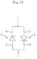
Figure 14 is a circuit diagram for illustrating a protective
circuit in the LED lamp according to the ninth embodiment;
Figure 15A is a plan view showing the structure of a GaN
LED element according to the ninth embodiment and Figure 15B
is a cross-sectional view taken along the line J-J thereof;
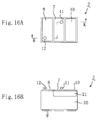
Figure 16A is a plan view showing the structure of a Si
diode element according to the ninth embodiment and Figure
16B is a cross-sectional view taken along the line K-K
thereof;
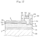
Figure 17 is a cross-sectional view showing the respective
structures of a GaN LED element and a diode element according
to a tenth embodiment of the present invention;
Figure 18 is a cross-sectional view showing the respective
structures of a GaN LED element and a diode element according
to an eleventh embodiment;
Figure 19 is a cross-sectional view showing the respective
structures of a GaN LED element and a diode element according
to a twelfth embodiment of the present invention;
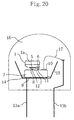
Figure 20 is a cross-sectional view of a semiconductor
light-emitting device according to another embodiment of the
present invention;
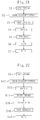
Figure 21 is a flow chart illustrating a manufacturing
method according to a thirteenth embodiment of the present
invention;
Figure 22 is a flow chart illustrating a manufacturing
method according to a fourteenth embodiment of the present
invention;
Figure 23 is a flow chart illustrating a manufacturing
method according to a fifteenth embodiment of the present invention;
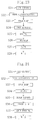
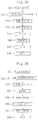
Figure 24 is a flow chart illustrating a manufacturing
method according to a sixteenth embodiment of the present invention;
Figure 25 is a flow chart illustrating a manufacturing
method according to a nineteenth embodiment of the present
invention;
Figure 26 is a flow chart illustrating a manufacturing
method according to a twentieth embodiment of the present invention;
Figure 27 is a cross-sectional view diagrammatically
showing the relations among a wafer, an LED element, and a
jig for conveying the LED element in a chip bonding process
step;
Figure 28 is a cross-sectional view diagrammatically
showing the relation between the wafer and a capillary 102 in
the process step of stud bump formation;
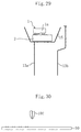
Figure 29 is a cross-sectional view showing the LED element
aligned with a Si diode element on a mount portion in
the chip bonding process step;
Figure 30 is a cross-sectional view diagrammatically
showing the relation between a wafer 90 and the capillary 102
in the process step of stud bump formation;
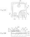
Figure 31A is a plan view of an LED element used in the
thirteenth embodiment and Figure 31B is a cross-sectional
view taken along the line L-L thereof;
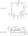
Figure 32A is a plan view of an LED element with microbumps
formed by a plating method and Figure 32B is a cross-sectional
view taken along the line M-M thereof;
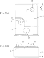
Figure 33A is a plan view of a Si diode element, on
which stud bumps are formed, and Figure 33B is a cross-sectional
view taken along the line N-N thereof;
Figure 34 is a flow chart illustrating a manufacturing
method according to a twenty-first embodiment of the present
invention; and
Figure 35 is a cross-sectional view diagrammatically
showing the relations among a wafer, a probe, and an photodetector
in the process step of an optical characteristic test.
BEST MODE FOR CARRYING OUT THE INVENTION
LIGHT-EMITTING ELEMENT
A light-emitting element according to the present invention
comprises one microbump formed on a first electrode and
at least another microbump formed on a second electrode. The
reason for only one microbump on the first electrode is to
minimize the area occupied by the first electrode and maximize
the light-emitting area of the light-emitting element.
Preferably, a columnar or mushroom-shaped microbump having a
diameter on the order of 30 to 40 µm (hereinafter referred
to as "dotted microbump") is formed on the first electrode.
In accordance with the present invention, the number of
the microbumps on the second electrode is one or more. This
is for stably supporting the chip of the semiconductor light-emitting
element such as the GaN LED element by means of the
dotted microbump provided on the first electrode and the microbump
or microbumps provided on the second electrode and
thereby preventing the chip from tilting. To achieve the
purpose, in the case of forming dotted microbumps on the second
electrode, the number of the dotted microbumps is preferably
two or more. In the case of forming a series of
dotted microbumps into a linear configuration (the resulting
microbump is hereinafter referred to as a "linear microbump")
or forming a series of dotted microbumps into a planar configuration
(the resulting microbump is hereinafter referred
to as a "planar microbump"), only one "linear" or "planar"
microbump is sufficient.
The maximum lateral dimension of a microbump is preferably
in the range of 5 to 300 µm and the height thereof is
preferably in the range to 5 to 50 µm. The maximum lateral
dimension is preferably 5 µm or more for the ease of formation
in forming the microbump by plating. The maximum lateral
dimension of a microbump is preferably 300 µm or less.
Preferably, the dotted microbump is configured as a circle
having a diameter of 30 to 40 µm or a polygon included in
the circle. Preferably, the linear microbump has a width of
20 to 30 µm and a length of 150 to 200 µm.
The height of a microbump is preferably 5 µm or more because
the chip of the semiconductor light-emitting element is
bonded to a leadframe or the like via microbumps in accordance
with a method in which the microbumps are welded with
the application of load, heat, and ultrasonic waves. If the
height of a microbump is under 5 µm, there is the possibility
that the chip is brought into contact with the leadframe at a
portion other than the bumps, which may cause a short-circuit
failure. On the other hand, the height of a microbump is
preferably 50 µm or less because the microbump having a
height of this order can be formed easily by using a plating
method. More preferably, the height of a microbump is 20 to
30 µm.
In dividing a wafer, in which semiconductor light-emitting
elements are formed, into individual chips and
mounting the chips on leadframes or the like in an assembly
process, if dotted microbumps are provided, each of the chips
placed with the microbumps facing downward is supported at
least three points by one microbump formed on the first electrode
and by two microbumps formed on the second electrode,
so that the chip is prevented from tilting. In this case,
the three microbumps are preferably positioned to form the
three vertices of the largest isosceles triangle that can be
included in the chip.
In the case of forming one dotted microbump on the first
electrode and one microbump on the second electrode, if the
microbump on the second electrode is formed into the linear
or planar microbump, the chip is supported at three or more
points and prevented from tilting. This eliminates a chip
recognition error and an arm pick-up error during the die-bonding
process step.
In contrast to the microbump or microbumps provided on
the second electrode which can be formed into plural dotted
microbumps, a linear microbump, or a planar microbump in
various configurations, the microbump provided on the first
electrode is preferably formed into a single dotted microbump.
This aims at minimizing the area occupied by the first
electrode and maximizing the light-emitting area.
In the light-emitting element according to the present
invention, even when the chip is bonded to the leadframe or
the like via Au microbumps which are welded with the application
of load, heat, and ultrasonic waves, the chip is never
brought into contact with the leadframe at a portion other
than the bumps, so that a short-circuit failure does not occur.
Preferably, metal having excellent adhesion to a first-conductivity-type
semiconductor region and/or a second-conductivity-type
semiconductor region is placed under the
first electrode and/or the second electrode, on which the microbumps
are formed. This prevents the problem of peeling
off of the electrode due to an ultrasonic wave used along
with load and heat in the process step of welding and bonding
Au microbumps to bond the chip of the semiconductor light-emitting
element to the leadframe via the microbumps. In the
case where the first-conductivity-type semiconductor region
is of n-type GaN and the second-conductivity-type semiconductor
region is of p-type GaN, Ti is the metal having excellent
adhesion. The use of Ti is also advantageous in that Ti
forms an excellent n-type GaN ohmic contact electrode.
On the top faces of the first and second electrodes, not
only the regions where the microbumps are formed, but also
respective regions (probe regions) to come into contact with
a probe needle may be formed. This prevents the probe needle
from touching and destroying the microbumps in the process
step of a probe test. Each of the probe regions should have
an area of at least 50×50 µm. On the top face of the second
electrode, the probe region can be formed easily. In the
case of the first electrode, however, the area of the probe
region is preferably minimized.
The probe region of the first electrode may be formed to
extend over a part of a dicing street. This allows the first
electrode to be formed sufficiently large to carry a columnar
or mushroom-shaped microbump having a diameter on the order
of 30 to 40 µm and maximizes a light-emitting area. In this
case, the dicing street is formed to expose the n-type GaN
layer. Although it is possible to separate the first electrode
into the region in which the microbump is formed and
the probe region, the first electrode is preferably not separated
with the two regions disposed contiguous to each other,
which allows a more accurate characteristic test to be performed.
The second electrode may be formed to include an opening
through which light is emitted from the light-emitting element.
This allows light emitted through the opening to reach
a detector positioned above such that the intensity and wavelength
of the light are measured thereby. Preferably, the
opening formed in the second electrode is configured as a
circle having a diameter of 20 µm or less or a polygon included
in the circle. This is because, if the opening is excessively
large and the second-conductivity-type
semiconductor region (p-type GaN layer) is excessively thin,
current in sufficient quantity cannot be injected in the active
layer and a sufficient amount of light cannot be obtained,
which leads to degraded brightness. Conversely, a
sufficient amount of light cannot also be obtained if the
opening is excessively small, so that it is appropriate to
form a plurality of openings in a mesh pattern.
A conductive transparent electrode may be formed in the
opening formed in the second electrode to make an ohmic contact
with the second-conductivity-type semiconductor region.
This achieves current injection in the InGaN active layer and
emission of light.
It will easily be appreciated that the opening need not
be formed any more if it is possible to change the position
of the detector of the prober and place it under the wafer.
The substrate may be made of a material transparent under
the light emitted from the light-emitting element. This
permits the light emitted from within the element to be obtained
from the substrate side and efficient emission of
light with a flip-chip structure. In the case where the
light-emitting element is made of a GaN-based compound semiconductor,
the substrate is preferably made of sapphire.
Since an excellent crystallographic compatibility is observed
between a GaN crystal and a sapphire crystal and the sapphire
substrate is a transparent insulating substrate, the resulting
flip-chip light-emitting element is excellent in the
property of emitting light including blue light. The sapphire
substrate is also superior and convenient in terms of
light-emitting efficiency since the refractive index of the
sapphire substrate, which is 1.77, is between the refractive
index of GaN, which is 2.1, and the refractive index of a
mold resin, which is 1.5.
Referring now to the accompanying drawings, the light-emitting
element according to each of the embodiments of the
present invention will be described.
Embodiment 1
Figure 1 is a plan view of a GaN LED element 1 according
to the present embodiment and Figure 2 is a cross-sectional
view taken along the line A-A thereof. As shown in the drawings,
the GaN LED element 1 has a double heterostructure comprising
a GaN buffer layer 31, an n-type GaN layer 32, an
InGaN active layer 33, a p-type AlGaN layer 34, and a p-type
GaN layer 35 which are stacked sequentially in layers on the
top face of a sapphire substrate 30. The top face of the n-type
GaN layer 32 has a stepped configuration consisting of
an upper-level portion occupying the major part of the top
face and a lower-level portion occupying the remaining minor
part thereof. An n-side electrode 6 made of a Ti/Au multilayer
film and a Ni/Au multilayer film laminated thereon is
formed in stacking relation on the top face of the lower-level
portion of the n-type GaN layer 32. The aforesaid InGaN
active layer 33, p-type AlGaN layer 34, and p-type GaN
layer 35 are stacked sequentially in layers on the top face
of the upper-level portion of the n-type GaN layer 32. A p-side
electrode 5 made of Ni and Au is disposed directly on
the top face of the p-type GaN layer 35 with no intervention
of a transparent electrode for current diffusion. The GaN
LED element 1 according to the present embodiment is typically
configured as a square with sides on the order of 0.28 mm.
Microbumps 22 and 23 made of Au or an Au alloy are formed on
the n-side electrode 6 and on the p-side electrode 5, respectively.
Figure 3 is a cross-sectional view schematically showing
an LED device formed by mounting the GaN LED element 1 on
leadframes by a microbump bonding method. Two die pads 17a
and 17b insulated and separated from each other are provided
on the respective tips of the leadframes 13a and 13b. The
GaN LED element 1 is mounted on the die pads 17a and 17b with
the microbumps 23 and 22 in contact with the respective die
pads 17a and 17b. The GaN LED element 1 is fixed to the die
pads 17a and 17b with a UV curable insulating resin 16.
Light emitted from a light-emitting region is reflected
upward by the leadframe 13a, transmitted by the sapphire substrate
30, and obtained from above. The respective side ends
of the leadframes 13a and 13b are provided with reflectors
15a and 15b for upwardly reflecting light leaking laterally
of the GaN LED element 1.
A method of manufacturing the LED device according to
the present embodiment will be described below.
The description will be given first to a method of fabricating
the LED element.
As stated previously, the wafer having the double heterostructure
including the GaN buffer layer 31, the n-type
GaN layer 32, the InGaN active layer 33, the p-type AlGaN
layer 34, and the p-type GaN layer 35 stacked sequentially in
layers is formed on the top face of the sapphire substrate
30. A SiO2 resist mask with an opening corresponding to a
region to be selectively removed is formed on the surface of
the p-type GaN layer 35 of the wafer. Then, dry etching is
performed by using the SiO2 mask to selectively and partially
remove each of the p-type GaN layer 35, the p-type AlGaN
layer 34, the InGaN active layer 33 in the vertical direction.
Subsequently, the n-type GaN layer 32 is recessed from
the surface thereof to a slightly lower level, whereby the
whole structure is formed into the stepped configuration.
The description will be given next to an exemplary procedure
for forming the p-side electrode 5, the n-side electrode
6, and the microbumps 22 and 23 on the GaN LED element
1.
To form the n-side electrode 6 on the top face of the n-type
GaN layer 32, a Ti film with a thickness of about 0.2 µm
and an Au film with a thickness of about 0.5 µm are stacked
in this order by a lift-off method or an etching method.
The resulting multilayer film is then patterned into a circular
configuration having a diameter on the order of 50 µm.
A Ni film with a thickness of about 0.2 µm is further formed
over the entire surface of the wafer, followed by an Au
film with a thickness of about 1 µm formed thereon by vapor
deposition. Thereafter, a resist mask with openings corresponding
to the respective regions, in which the microbumps
are formed, is formed over the Ni/Au multilayer film by a
photolithography process step. The regions in the openings
of the resist masks are selectively plated with Au or an Au
alloy so that the mushroom-shaped microbumps 22 and 23 each
having a diameter of 30 µm and a height of 20 µm are formed
to overlie the n-side and p- side electrodes 6 and 5, respectively.
After that, the Ni film and the Au film are selectively
etched away except for the portions thereof covering
substantially entirely the p-type GaN layer 35 and covering
the n-side electrode.
The description will be given next to the procedure for
mounting the GaN LED element 1 on the leadframes 13a and 13b.
The GaN LED element 1 is opposed to the die pads 17a and
17b of the leadframes 13a and 13b with the face thereof, on
which the microbumps 22 and 23 are formed, facing downward
and with the back face of the sapphire substrate 30 facing
upward, e.g., in a flip-chip configuration. The microbump 23
on the p-side electrode 5 is aligned with the die pad 17a,
while the microbump 22 on the n-side electrode 6 is aligned
with the die pad 17b. The UV curable insulating resin 16 is
then applied to the die pads 17a and 17b or to the GaN LED
element 1 and cured under the radiation of UV light, while
the GaN LED element 1 is pressed against the die pads 17a and
17b. It is also possible to cut off the die pads 17a and 17b
after the mounting of the GaN LED element 1.
In the LED device internally provided with the GaN LED
element 1 according to the present embodiment, the p-side
electrode 5 and the n-side electrode 6 are formed on one side
thereof and the microbumps 22 and 23 are formed on the p-side
and n- side electrodes 5 and 6, respectively. By thus connecting
the GaN LED element 1 to such members as leadframes
via the microbumps 22 and 23, the following effects can be
achieved.
In general, a microbump can easily be scaled down to
have a diameter on the order of 10 µm, which eliminates the
necessity for a bonding pad that has been required by a conventional
element. Consequently, the electrode structure can
be miniaturized and the light-emitting element (the GaN LED
element 1 in the present embodiment) can be reduced in size.
Owing to the size reduction, the amount of a costly material
used in the sapphire substrate 30 or a compound semiconductor
substrate is also reduced, resulting in lower cost. Moreover,
since the n-side electrode 6 can also be reduced in
size, the light-emitting region within the GaN LED element 1,
i.e., a pn junction region is enlarged, so that higher
brightness is achieved than in the conventional element of
the same size. Furthermore, since the back face of the sapphire
substrate, opposite to the face on which the electrodes
5 and 6 are formed, serves as the light-emitting face and
light is emitted therefrom in the direction indicated by the
arrows in Figure 3, improved light-emitting efficiency is
achieved in the absence of members preventing light emission
such as the electrode.
The description will be given to a preferred configuration
of the microbump characterizing the present embodiment.
As stated previously, each of the microbumps 22 and 23 has a
diameter preferably in the range of 5 to 300 µm and, more
preferably, in the range of 5 to 100 µm. If each of the microbumps
22 and 23 has a diameter exceeding 100 µm, the area
occupied thereby is increased so that flip-chip bonding has
no more advantage over wire bonding. Most preferably, the
diameter of the microbump is in the range of 10 to 30 µm. If
each of the microbumps 22 and 23 has a columnar configuration,
the height thereof is preferably 30 µm or less. If
each of the microbumps 22 and 23 has a mushroom-like configuration,
on the other hand, the height thereof is preferably
50 µm or less. This is because a thick resist film is required
to form the columnar microbumps by a selective plating
technique, but it is difficult to form a resist film with a
thickness of 30 µm or more by the photolithography process
step. If plating is performed to reach a height exceeding 50
µm to form the mushroom-shaped microbumps, on the other
hand, the diameter of the cap portion of the mushroom-shaped
microbump is increased laterally to the order of 100 µm, so
that flip-chip bonding has only reduced advantages over wire
bonding.
Preferably, the n-side electrode 6 is formed to have a
circular cross section of such a size as to allow the formation
of the microbump 22 thereon, i.e., with a diameter
slightly larger than the diameter of the columnar microbump.
In the case where the diameter of the microbump is on the order
of 30 µm, e.g., the n-side electrode 6 is formed to have
a circular cross section with a diameter on the order of 50 µm
suitably for the scaling down of the LED element. It will
easily be appreciated that the transverse cross section of
the microbump is not necessarily be circular as in the present
embodiment but may be oval or generally square. In that
case, the lateral maximum dimension is appropriately in the
foregoing range for the diameter.
Since the back face of the sapphire substrate 30 serves
as the light-emitting face, it is no more necessary to form a
transparent electrode on the p-side electrode 5 as in the
conventional GaN LED element. Consequently, it is also possible
to provide the p-side electrode made of a thick film
over the entire surface of the p-type GaN layer 35.
The LED element fabricated in accordance with the foregoing
method is typically configured to have a square cross
section with 0.28 mm sides in which the area surrounding the
n-side electrode and not contributing to light emission accounts
for 1/15 of the surface area of the element. The conventional
element is typically configured to have a square
cross section with 0.34 mm sides in which the area not contributing
to light emission accounts for 1/2 of the surface
area of the element. In short, the element according to the
present embodiment has a light-emitting area 1.26 times
larger than that of the conventional element, though it has
an element size 0.68 times smaller than that of the conventional
element.
In the manufacturing method according to the present embodiment,
since metal used only in the p-side electrode (Ni
and Au) is further laminated on metal used only in the n-side
electrode (Ti and Au) and the top face of the metal used only
in the p-side electrode is selectively plated with metal composing
the microbump, the conditions for selective plating
are equalized. As a result, the p-side electrode 5 is made
of the metal used only in the p-side electrode, while the n-side
electrode 6 is made of the metal used only in the n-side
electrode and the metal used only in the p-side electrode
laminated thereon. Consequently, a difference in level between
the top face of the p-type GaN layer 35 and the n-type
GaN layer 32 is reduced advantageously so that the tips of
the two microbumps 22 and 23 are on substantially the same
level. However, the method of manufacturing the light-emitting
element according to the present invention is not
limited to such an embodiment. Each of the p-side electrode
and the n-side electrode may be made of the metal used only
therein. A method of depositing metal composing the microbumps
is not limited to selective plating, either. It is also
possible to deposit a metal film by vapor deposition or
like method and remove the metal film surrounding the microbumps
together with the resist film to leave only the microbumps.
Although the GaN LED element is mounted on the leadframes
in the foregoing embodiment, the present invention is
not limited thereto. For example, it is also possible to
mount the GaN LED element on an active element, a passive
element, or a base substrate by flip-chip connection or alternatively
mount other active and passive elements on the
GaN LED element by flip-chip connection.
The light-emitting element according to the present invention
is not limited to the GaN LED element but may be another
light-emitting element. However, since the GaN LED
element is formed on a transparent and insulating sapphire
substrate and the p-side electrode and the n-side electrode
are formed on one side thereof, it can exert remarkable effects
if the present invention is applied thereto.
The substrate of the light-emitting element according to
the present invention is not necessarily transparent because,
if the substrate is opaque, it is sufficient to obtain light
from the opposite side of the substrate. However, the substrate
made of a transparent material improves light-emitting
efficiency, as described above, since it allows light to be
obtained from the side opposite to the p-side and n-side
electrodes.
In the process step of a probe test for testing the
characteristics of the GaN LED element and in the assembly
process step for dividing the wafer into individual chips and
mounting them on leadframes or the like, there are possibilities
that the following problems occur, which can be subdivided
into three types.
The first type of problems occur in the assembly process.
In the case of dividing the wafer, in which GaN LED
elements are formed, into individual chips (in each of which
one GaN LED element is formed) and mounting each of the chips
on leadframes or the like, the arms of a die bonder or the
like recognize the chip placed with the microbumps facing
downward and come to pick it up. In that case, however, the
chip supported by the two microbumps is likely to tilt, which
may lead to trouble associated with the chip recognition and
pick-up operation performed by the arms. On the other hand,
if the chip is bonded to leadframes or the like via the microbumps
in accordance with a method in which the Au microbumps
are welded and bonded with the application of load,
heat, and ultrasonic waves, the microbumps of reduced heights
may result in an undesired contact between the chip and the
leadframes at a portion in which the microbumps are not
formed. Such an undesired contact causes the problems of a
short-circuit failure and the peeling off of the electrode
due to the ultrasonic wave.
The second type of problems occur in the process step of
a probe test. As stated above, the light-emitting area can
be maximized when the n-side electrode 6 of the GaN LED element
is in minimum size. For this purpose, the electrode is
preferably sized to allow one columnar or mushroom-shaped microbump
with a diameter on the order of 30 µm to be formed
thereon. In this case, the n-side electrode 6 is preferably
configured as a circle having a diameter on the order of 60 µm.
However, the microbump may be destroyed by a probe needle
in contact therewith in the process step of a probe test for
testing the characteristics of the element.
The third type of problems also occur in the process
step of a probe test. In the case of performing a probe test
by means of a normal prober, a wafer, in which GaN LED elements
are formed, are placed on a stage with the electrodes
facing upward and fixed with a vacuum chuck. The characteristics
of the element are tested by bringing the probe needle
into contact with the electrodes from above the wafer. However,
since light is obtained from the back face of the sapphire
substrate of the GaN LED element and a detector for
measuring the intensity and wavelength of light is disposed
above the stage, the amount of light reaching the detector
positioned above the stage may be insufficient.
The following embodiment relates to a light-emitting
element with a flip-chip structure, in which microbumps are
formed and which allows the test process and the assembly
process to be performed without trouble.
Embodiment 2
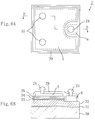
Figure 6A is a plan view of a GaN LED element 1 according
to the present embodiment and Figure 6B is a cross-sectional
view taken along the line D-D thereof. The present
embodiment is characterized in that one dotted microbump is
formed on the n-side electrode 6 of the GaN LED element 1 and
that two dotted microbumps are formed on the p-side electrode
5 thereof.
Referring to Figures 6A and 6B, a detailed description
will be given to the structure. As shown in the drawings,
the GaN LED element 1 has a double heterostructure including
a GaN buffer layer 31, an n-type GaN layer 32, an InGaN active
layer 33, a p-type AlGaN layer 34, and a p-type GaN
layer 35, which are stacked sequentially in layers on the top
face of a sapphire substrate 30. The top face of the n-type
GaN layer 32 has a stepped configuration consisting of a upper-level
portion occupying the major part of the top face
and a lower-level portion occupying the remaining minor part
thereof. An n-side electrode 6 made of a Ti/Au multilayer
film and a Mg/Au multilayer laminated thereon is formed on
the top face of the lower-level portion of the n-type GaN
layer 32. The aforesaid InGaN layer 33, p-type AlGaN layer
34, and p-type GaN layer 35 are stacked sequentially in layers
on the top face of the upper-level portion of the n-type
GaN layer 32. A p-side electrode 5 made of Mg and Au is
provided directly on the top face of the p-type GaN layer 35
with no intervention of a transparent electrode. One dotted
microbump 24 made of Au or an Au alloy is formed on the top
face of the n-side electrode 6, while two dotted microbumps
25 made of Au or an Au alloy are formed on the top face of
the p-side electrode 5. The entire surface of the element is
covered with a protective film 39 except for the microbumps.
Each of the three dotted microbumps has a mushroom-like
or columnar configuration with a diameter of 40 µm and a
height of 20 µm. The three microbumps are positioned to
form the three vertices of the largest isosceles triangle
that can be included in the chip.
In the arrangement, the chip with the GaN LED element 1
is supported at three points by the microbumps and prevented
from tilting even in the case where it is placed with the microbumps
facing downward. Consequently, no chip recognition
error or arm pick-up error occurs during die bonding.
By setting the height of the microbump at 20 µm, the
process step of bonding the chip with the GaN LED element 1
to leadframes or the like with the application of lead, heat,
and an ultrasonic wave under proper bonding conditions is
free from a short-circuit failure resulting from an undesired
contact between the chip and the leadframe at a portion other
than the bumps, while a sufficient bonding strength is maintained.
Moreover, since Ti used in the n-side electrode and Mg
used in the p-side electrode are materials exhibiting excellent
adhesion to GaN, no peeling due to the ultrasonic wave
was observed.
Embodiment 3
Figure 7A is a plan view of a GaN LED element 1 according
to the present embodiment and Figure 7B is a cross-sectional
view taken along the line E-E thereof. The present
embodiment is characterized in that one dotted microbump 24
is formed on the n-side electrode 6 of the GaN LED element 1
and that one linear microbump 25a is formed on the p-side
electrode 5 thereof. As for the other components, they are
the same as in the second embodiment.
The linear microbump 25a on the p-side electrode 5 has
a width of 20 µm, a length of 80 µm, a height of 20 µm, and a
mushroom-shaped or columnar cross section taken along the
line E-E.
In this case also, no chip recognition error or arm
pick-up error occurs during die bonding since the chip with
the GaN LED element 1 is supported by the microbumps and
thereby prevented from tilting.
Embodiment 4
Figure 8A is a plan view of a GaN LED element 1 according
to the present embodiment and Figure 8B is a cross-sectional
view taken along the line F-F thereof. The present
embodiment is characterized in that metal having excellent
adhesion to the p-type GaN layer is placed under the p-side
electrode to correspond to the microbumps disposed on the GaN
LED element 1. As for the other components, they are the same
as in the second embodiment.
In the case where a multilayer film of Ni, Au, or the
like is used as a material composing the p-side electrode 5,
Ni having poor adhesion to the GaN layer and forming the interface
with the p-type GaN layer underlying the p-side electrode
5 peels off at portions corresponding to the microbumps
25 and their vicinities due to an ultrasonic wave used along
with load and heat in the process step of welding and bonding
the microbumps to leadframes or the like. To prevent this,
metal 73 with excellent adhesion such as Ti is effectively
placed at portions corresponding to the microbumps 25 and
their vicinities to underlie the p-side electrode 5, which
prevents peeling in the bonding process step and maintains
sufficient bonding strength.
Although the present embodiment has described the
process step in which the microbumps is welded with the application
of load, heat, and ultrasonic wave as an exemplary
method of bonding the chip to leadframes or the like, the
bonding method is not limited thereto. The present embodiment
is also applicable to, e.g., a stud bump bonding (SBB)
method, to an ACF method using an anisotropic conductive
sheet or adhesive, and to a method using solder bumps.
Embodiment 5
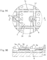
Figure 9A is a plan view of a part of a group of GaN LED
elements formed on a 2-inch wafer according to the present
embodiment and Figure 9B is a cross-sectional view taken
along the line G-G thereof. The present embodiment is characterized
in that the top faces of the p-side and n- side
electrodes 5 and 6 of the GaN LED element 1 are provided with
respective probe regions. In particular, the probe region
provided in the top face of the n-side electrode is formed to
extend over a dicing street.
In Figure 9A, the n-side electrode 6 is formed on the
top face of the lower-level portion of the n-type GaN layer
32 so as to extend over a part of a dicing street 37. On the
other hand, the p-side electrode 5 is formed over the substantially
entire top face of the p-type GaN layer 35. The
microbumps 24 and 25 each made of Au or an Au alloy are formed
on the n-side and p- side electrodes 6 and 5, respectively.
The surface of the element is coated with the
protective film 39 including respective openings corresponding
to the Au bump 25 on the p-side electrode 5, a probe region
5a provided in the top face thereof for contact with a
probe needle, the Au bump 24 on the n-side electrode 6, and a
probe region 6a provided in the top face thereof for contact
with a probe needle. The size of the probe region 5a of the
p-side electrode 5 is on the order of 70 x 80 µm, while the
size of the probe region 6a of the n-side electrode 6 is on
the order of 40 x 80 µm.
The probe region 6a of the n-side electrode 6 thus formed
to extend over the dicing street 71 allows a probe test
to be performed without damaging the microbump and maximizes
the light-emitting area of the GaN LED element 1.
Embodiment 6
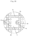
As shown in Figure 10, the present embodiment is the same
as the fifth embodiment except that a probe region 6b
separate and distinct from the n-side electrode 6 is provided
over the dicing street. Although the probe region 6b is
slightly smaller in size, it allows a probe test to be performed.
In this case also, the probe region 6b provided over
the dicing street enlarges the light-emitting area of the GaN
LED element 1. However, the probe region 6b allows a more
accurate characteristic test to be performed if it is not
separated from the n-side electrode 6.
Embodiment 7
Figure 11A is a plan view of a GaN LED element 1 according
to the present embodiment and Figure 11B is a cross-sectional
view taken along the line H-H thereof. The present
embodiment is characterized in that a plurality of openings
72 are formed in rows and columns in the center portion of
the p-side electrode 5 of the GaN LED element 1.
Each of the openings is configured as a circle with a
diameter of 10 µm. By thus arranging the openings in 5
rows and 3 columns, a sufficient amount of light required for
brightness and wavelength measurement can be supplied to the
detector.
The openings 72 need not necessarily be formed in the
center portion of the p-side electrode 5 but may be formed in
any portion of the p-side electrode provided that they can be
formed therein.
Embodiment 8
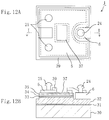
Figure 12A is a plan view of a GaN LED element 1 according
to the present embodiment and Figure 12B is a cross-sectional
view taken along the line I-I thereof. The present
embodiment has been achieved by replacing the openings 72 in
rows and columns according to the seventh embodiment with a
transparent electrode in ohmic contact with the p-type GaN
layer. In this case, the size of the transparent electrode
is 50 x 100 µm and a sufficient amount of light can be supplied
to the detector. It will easily be appreciated that
the size of the transparent electrode is not limited thereto.
SEMICONDUCTOR LIGHT-EMITTING DEVICE
In general, an LED lamp made of a semiconductor layer
provided on an insulating substrate as shown in Figure 5 is
susceptible to static electricity due to the physical constant
(e.g., dielectric constant ε ) of the material and
structure of the element. If the LED lamp is opposed to a
capacitor charged with static electricity and a discharge is
caused therebetween, the LED lamp will be destroyed by an
electrostatic voltage of 100 V in the forward direction and
with an electrostatic voltage of 30 V in the reverse direction.
Compared with an LED element made of another bulk compound
semiconductor (GaP, GaAlAs, or the like), the LED lamp
is destroyed by an extremely low electrostatic voltage. Unless
any protective treatment is performed with respect to
the LED lamp, static electricity applied from the outside to
the LED may readily break down the GaN LED element within the
LED lamp.
A description will be given to a highly reliable semiconductor
light-emitting device internally provided with the
function of preventing a destruction induced by the application
of a high voltage such as static electricity.
Embodiment 9
Figure 13 is a cross-sectional view of a semiconductor
light-emitting device (GaN-based LED lamp) according to the
present embodiment. The GaN-based LED lamp according to the
present embodiment is characterized in that a GaN LED element
1 is mounted on leadframes 13a and 13b with a Si diode element
2 having p-side and n-side electrodes interposed therebetween,
not directly on the leadframes.
As shown in Figure 13, the Si diode element 2 with the
main surface thereof facing upward and with the back face
thereof facing downward is disposed on a die pad forming the
tip of the leadframe 13a having a reflecting mirror. The Si
diode element 2 is die-bonded to the die pad with an Ag paste
14, while having an n-side electrode 9 on the back face
thereof in contact with the die pad of the leadframe 13a. A
p-side electrode 7, an n-side electrode 8, and a bonding pad
portion 10 of the p-side electrode are provided on the top
face of the Si diode element 2. The GaN LED element 1 having
the top face of the sapphire substrate facing downward and
the p-side and n- side electrodes 5 and 6 facing downward is
positioned above the Si diode element 2. The p-side and n- side
electrodes 5 and 6 of the GaN LED element 1 are electrically
connected to the n-side and p- side electrodes 8 and 7
of the Si diode element 2 via Au microbump 12 and 11, respectively.
The GaN LED element 1 is fixed to the Si diode element
2 with a UV curable insulating resin 16. The mechanical
connection between the GaN LED element 1 and the Si diode
element 2 may be accomplished by welding the microbumps 11
and 12 instead of using the UV curable insulating resin 16.
Such a welding process step will be described later. The
bonding pad portion 10 of the p-side electrode of the Si diode
element 2 is connected by wire bonding to the lead frame
13b via an Au wire 17. A reflector 15 for upwardly reflecting
light is attached to a side face of the die pad of the
leadframe 13a, whereby the GaN LED element 1 is surrounded.
The tip portions of the leadframes 13a and 13b are entirely
molded with a transparent epoxy resin 18 with the GaN
LED element 1 and the Si diode element 2 mounted thereon to
constitute the LED lamp. The light generated by the GaN LED
element 1 is emitted upward from the back face of the sapphire
substrate. As a result, such a transparent electrode
for current diffusion (the member designated at the reference
numeral 37 in Figures 4A, 4B, and 4C) as formed in the conventional
GaN LED element is no more necessary. As a member
for current diffusion, only the thick-film p-side electrode 5
is provided satisfactorily.
The light leaked laterally of the GaN LED element 1 is
reflected upward by the reflector 15 such that the light-emitting
efficiency is enhanced. For this purpose, the reflector
15 is preferably positioned to have the tip portion
thereof at least higher in level than the light-emitting region
of the GaN LED element 1.
Figure 14 is a circuit diagram for illustrating a protective
circuit provided in the LED lamp according to the
present embodiment.
As shown in Figure 14, the GaN LED element 1 is connected
to the Si diode element 2 in opposite-polarity relation,
i.e., the p-side and n-side electrodes of the GaN LED element
1 are connected to the n-side and p-side electrodes of the Si
diode element 2 having the opposite polarities, which prevents
a high voltage from being applied to the GaN LED element
1 from the leadframe side. In this case, the forward
operating voltage applied to the Si diode element 2 is about
0.9 V so that the reverse voltage for the GaN LED element 1
is cut off at 0.9 V. On the other hand, since the reverse
breakdown voltage for the Si diode element 2 can be set to a
value in the vicinity of 10 V, the forward voltage applied to
the GaN LED element 1 can also be cut off at a value in the
vicinity of 10 V. As described above, since the forward and
reverse breakdown voltages for the GaN LED element 1 are on
the order of 100 V and 30 V, respectively, the arrangement
surely prevents the destruction of the GaN LED element 1 induced
by the application of a high voltage such as static
electricity.
Specifically, when the forward and reverse destruction
voltages for the GaN LED element 1 are represented by Vf1 and
Vb1, respectively, the forward and reverse breakdown voltages
for the Si diode element 2 are represented by Vf2 and Vb2,
respectively, and the operating voltage for the GaN LED element
1 is represented by VF, the breakdown of the GaN LED
element 1 is prevented appropriately provided that the following
relationship is established:
Vf2 < Vb1 Vb2 < Vf1 Vb2 > VF.
A description will be given next to the detailed structures
of the individual components of the LED lamp according
to the present embodiment and to the outline of the manufacturing
process therefor.
Figure 15A is a plan view of the GaN LED element 1 according
to the present embodiment and Figure 15B is a cross-sectional
view taken along the line J-J thereof. As shown in
the drawings, the GaN LED element 1 has a double heterostructure
including a GaN buffer layer 31, an n-type GaN layer 32,
an InGaN active layer 33, a p-type AlGaN layer 34, and a p-type
GaN layer 35 which are stacked sequentially in layers on
the top face of the sapphire substrate 30. The top face of
the n-type GaN layer 32 has a stepped configuration consisting
of an upper-level portion occupying the major part of the
top face and a lower-level portion occupying the remaining
minor part thereof. An n-side electrode 6 made of Ti and Au
is formed on the top face of the lower-level portion of the
n-type GaN layer 32. The aforesaid InGaN active layer 33. p-type
AlGaN layer 34, and p-type GaN layer 35 are stacked sequentially
in layers on the top face of the upper-level portion
of the n-type GaN layer 32. A p-side electrode 5 is
disposed directly on the top face of the p-type GaN layer 35
with no intervention of a transparent electrode for current
diffusion. The GaN LED element 1 according to the present
embodiment is typically configured as a square with sides on
the order of 0.28 mm in two dimensions.
Figure 16A is a plan view of the Si diode element 2 according
to the present embodiment and Figure 16B is a cross-sectional
view taken along the line K-K thereof. As shown in
Figures 16A and 16B, a p-type semiconductor region 21 is formed
by selectively implanting impurity ions into an n-type
silicon substrate 20 of the Si diode element 2. The reverse
breakdown voltage for the Si diode element 2 is set at a value
in the vicinity of 10 V. Thereafter, the p-side and n- side
electrodes 7 and 8 of the Si diode element 2 are formed
on the p-type semiconductor region 21 and on the n-type silicon
substrate 20 (n-type semiconductor region), respectively.
A part of the p-side electrode 7 forms the bonding pad portion
10. The n-side electrode 9 for providing an electrical
connection with the leadframe is formed on the back face of
the n-type silicon substrate 20. The two-dimensional size of
the Si diode element 2 according to the present embodiment is
on the order of 0.32 x 0.45 mm.
Next, the procedure for mounting the GaN LED element 1
on the Si diode element 2 will be described.
The description will be given first to the procedure for
forming the Au microbumps for providing electrical connections
between the electrodes of the GaN LED element 1 and the
electrodes of the Si diode element 2. The microbumps 11 and
12 are formed on the p-side and n- side electrodes 7 and 8 on
the top face of the Si diode element 2 by selectively plating
with Au only the top faces of the electrodes 7 and 8 masked
with a photoresist film patterned by a photolithography
process step. Each of the microbumps 11 and 12 according to
the present embodiment has a mushroom-like configuration having
a diameter on the order of 30 µm and a height on the order
of 10 µm.
Next, the GaN LED element is positioned above the Si diode
element 2, while having the n-side and p- side electrodes
6 and 5 thereof opposed to the p-side and n- side electrodes 7
and 8 of the Si diode element 2, respectively. Then, an UV
curable insulating resin 16 is interposed between the GaN LED
element and the Si diode element and irradiated with UV
light, while the GaN LED element 1 is pressed thereto, thereby
fixing the two elements 1 and 2 to each other and providing
electrical connections between the corresponding
electrodes of the elements 1 and 2. By thus performing a
flip-chip connecting process step in accordance with the
foregoing microbump bonding method, there is formed a composite
device made of the electronic device paired up with the
optical device.
Subsequently, as shown in Figure 13, the composite device
is die-bonded onto the leadframe 13a with the Ag paste
14. After that, a wire bonding process step is performed to
provide a connection between the bonding pad portion 10 of
the p-side electrode 7 and the leadframe 13b via the Au wire
17. However, it is also possible to perform the wire bonding
process step first and then the foregoing flip-chip connecting
process step.
Finally, a resin molding process step is performed by
using the transparent epoxy resin 18 to provide the light-emitting
device shown in Figure 1.
Since the present embodiment has constituted the composite
device by connecting the GaN LED element 1 to the Si diode
element 2 in the opposite-polarity relation, as described
above, the reverse voltage applied to the GaN LED element 1
can be cut off at a value in the vicinity of the forward
voltage applied to the Si diode element 2, while the forward
voltage applied to the GaN LED element 1 can be cut off at a
value in the vicinity of the reverse break down voltage for
the Si diode element 2, so that the destruction of the GaN
LED element 1 due to static electricity is surely prevented.
Moreover, since the present embodiment has composed the
composite device by mounting the GaN LED element 1 on the Si
diode element 2 by flip-chip bonding in accordance with the
microbump bonding method, a large bonding pad portion for
wire bonding is no more necessary to provide a connection
therebetween, which achieves the scaling down of the whole
composite device and a reduction in the area of the n-side
electrode 6 not contributing to light emission and a surrounding
portion thereof. Specifically, the area of the n-side
electrode 6 and the surrounding portion thereof occupies
only 1/15 of the surface area of the GaN LED element 1 in the
present embodiment. By contrast, the area of the n-side
electrode 36 not contributing to light emission and the surrounding
portion thereof occupies 1/2 of the surface area of
the conventional GaN LED element 1 shown in Figure 4A if the
element is assumed to have a square cross section with 0.34
mm sides. In short, the GaN LED element 1 according to the
present embodiment has an enlarged light-emitting area which
is 1.26 times the light-emitting area of the conventional GaN
LED element 1 shown in Figures 4A and 4B, though it has a reduced
size which is 0.68 times the size of the conventional
GaN LED element 1. By thus providing the flip-chip connection
in accordance with the microbump bonding method, the
area of a costly compound semiconductor substrate can be reduced,
resulting in lower cost and an enhanced light-emitting
ability.
Since light can be emitted from the back face of the
transparent sapphire substrate in the present embodiment,
there can also be achieved the advantage of improved light-emitting
efficiency.
Although the p-side electrode 7 is disconnected from the
bonding pad portion 10 in the present embodiment, they may be
formed integrally. The present embodiment has the advantage
of easily and surely preventing the UV curable insulating
resin 16 from spreading to the bonding pad portion 10 with a
midway groove. In the case of performing the wire bonding
process step first and then the flip-chip connecting process
step, however, the formation of the bonding pad portion 10
integral with the portion of the p-side electrode 7, on which
the microbump 11 is formed, has the advantage over the present
embodiment, since the UV curable insulating resin 16
spreading to the bonding pad portion 10 causes no trouble but
has the advantage of stably maintaining the bonding pad portion
10 and the p-side electrode 7 at the same potential.
Since the p-side electrode 5 of the GaN LED element 1 is
opposed to the n-side electrode 8 of the Si diode element 2
in the present embodiment, light emitted from the light-emitting
layer underlying the p-side electrode 5 can be reflected
upward by the n-side electrode 8, resulting in improved
light-emitting efficiency.
Although the foregoing description has been given to the
embodiment in which the microbumps 11 and 12 are formed on
the p-side and n- side electrodes 7 and 8 of the Si diode element
2, it will easily be appreciated that the microbumps 11
and 12 may also be formed on the p-side and n- side electrodes
5 and 6 of the GaN LED element 1.
Preferably, the n-side electrode 8 on the Si diode element
2 is in maximum size and opposed to the p-side electrode
5 of the GaN LED element 1, since the light-emitting efficiency
can further be improved by upwardly reflecting light
leaked laterally of the GaN LED element 1.
Although the present embodiment has configured the p-side
and n-side electrodes on the top face of the Si diode 2
as rectangles separated from each other in one direction,
i.e., arranged in parallel with each other, the present invention
is not limited to the embodiment. The p-side and n-side
electrodes on the top face of the Si diode element 2 may
also have triangular configurations diagonally separated from
each other in two dimensions or curved configurations.
Embodiment 10
Although the ninth embodiment has mounted the GaN LED
element on the Si diode element, the present embodiment
provides a Si diode element made of a thin film on a GaN LED
element.
Figure 17 is a cross-sectional view showing only the device
portion of an LED lamp according to the present embodiment.
The device portion is to be mounted on leadframes and
finally molded with a resin in the same configuration as
shown in Figure 1 illustrating the first embodiment, though
the drawing of the device portion mounted on the leadframes
will be omitted.
As shown in Figure 17, an interlayer insulating film 51
made of a silicon oxide film is formed on the GaN LED element
1 having the same structure as in the ninth embodiment and a
silicon thin film is formed thereon. In the silicon thin
film, a p-type semiconductor region 52 and an n-type semiconductor
region 53 are formed. The silicon thin film can be
formed easily by utilizing TFT formation technology associated
with a liquid-crystal device. The diode element 50 is
provided with a p-side electrode 54 filling in a through hole
formed in the interlayer insulating film 51 to be connected
to the n-side electrode 6 of the GaN LED element 1, while being
connected to the p-type semiconductor region 52 thereof.
The diode element 50 is also provided with an n-side electrode
55 filling in a though hole formed in the interlayer
insulating film 51 to be connected to the p-side electrode 5
of the GaN LED element 1, while being connected to the n-type
semiconductor region 53 thereof. The p-side and n- side electrodes
54 and 55 of the diode element 50 are connected to
leadframes by wire bonding, though the drawing thereof is
omitted. In this case, light generated by the GaN LED element
1 is reflected by the leadframes and emitted upward.
However, since the diode element 50 can be formed in a narrow
limited region, desired light-emitting efficiency can easily
be achieved.
The present embodiment also achieves the same effects as
the ninth embodiment does.
Embodiment 11
An eleventh embodiment will be described. A light-emitting
device according to the present embodiment has the
same Si diode element as used in the ninth embodiment which
is mounted on the silicon substrate without being opposed to
the diode element.
Figure 18 is a cross-sectional view showing the structure
of only the device portion of an LED lamp according to
the present embodiment. The device portion is to be mounted
on leadframes and finally molded with a resin in the same
configuration as shown in Figure 13 illustrating the ninth
embodiment, though the drawing of the device portion mounted
on the leadframes will be omitted.
As shown in Figure 18, the Si diode element 2 is formed
in the n-type silicon substrate 20 larger in area than in the
ninth embodiment. Specifically, the p-type semiconductor region
21 is formed by selectively implanting impurity ions into
the n-type silicon substrate 20. After the interlayer
insulating film 57 is formed, the p-side electrode 58 for
contact with the p-type semiconductor region 21 is formed on
the interlayer insulating film 57. The n-side electrode for
contact with the n-type silicon substrate 20, i.e., with the
n-type semiconductor region is also formed in a portion other
than the cross section shown in Figure 18, though the drawing
thereof is omitted. It is to be noted that the reverse
breakdown voltage and forward voltage for the Si diode element
2 are set to the same values as in the ninth embodiment.
On the other hand, the GaN LED element 1 having basically
the same structure as in the ninth embodiment is disposed
on the silicon substrate 20. However, the n-side electrode 6
of the GaN LED element 1 is formed larger in size to have a
sufficient area to allow wire bonding. The n-side electrode
6 of the GaN LED element 1 is connected to the p-side electrode
58 of the Si diode element 2 via a wire 59, while the
p-side electrode 5 of the GaN LED element 1 is connected to
the n-side electrode of the Si diode element 2 via a wire in
a portion not shown in Figure 18. In the present embodiment,
light is emitted from the GaN LED element 1 upwardly of the
p-side electrode 6.
Connections between the individual semiconductor regions
of the diode element 2 and the individual electrodes of the
GaN LED element 1 may also be achieved by forming a multilayer
wiring structure as formed in the tenth embodiment.
Although the effects of minimizing the whole light-emitting
device and improving the light-emitting efficiency
achieved by the present embodiment are inferior to those
achieved by the ninth embodiment, there can be implemented a
light-emitting device capable of exerting voltage resistance
to static electricity or the like, similarly to the ninth embodiment,
in accordance with the method not using microbumps.
Embodiment 12
A twelfth embodiment will be described. The present embodiment
forms a GaN LED element and a diode element on a
single common insulating substrate.
Figure 19 is a cross-sectional view showing the structure
of only the device portion of an LED lamp according to
the present embodiment. The device portion is to be mounted
on leadframes and finally molded with a resin in the same
configuration as shown in Figure 13 illustrating the ninth
embodiment, though the drawing of the device portion mounted
on the leadframes will be omitted.
As shown in Figure 19, the GaN LED element 1 having the
same structure as in the ninth embodiment is formed on a sapphire
substrate 30. A diode 60 including a p-type semiconductor
region 61 and an n-type semiconductor region 62 each
formed in a silicon thin film is further formed on the sapphire
substrate 30 laterally of the GaN LED element 1. The
silicon thin film on the sapphire substrate 30 can be formed
easily by utilizing, e.g., TFT formation technology associated
with a liquid-crystal device. A connection between the p-type
semiconductor region 61 of the diode element 60 and the
GaN LED element 1 may also be achieved by forming a multilayer
wiring structure as formed in the tenth embodiment or by
wire bonding as performed in the eleventh embodiment.
Because the sapphire substrate 30 is high in melting
point, the present embodiment has the advantage of forming a
silicon single-crystal thin film extremely easily by a laser
recrystallization method after the deposition of a polysilicon
film. Moreover, since the present embodiment can easily
be constituted such that light is emitted from the underlying
sapphire substrate, it is possible to maintain high light-emitting
efficiency even when the GaN LED element 1 is connected
to the diode element 60 by wire bonding.
Variations of Embodiments 9 to 12
The foregoing embodiments can be modified to provide the
following variations.
The structure according to the ninth embodiment may be
modified such that the surface of the n-side electrode 8 of
the Si diode 2 is entirely opposed to the surface of the p-side
electrode 5 of the GaN LED element 1 in planar symmetrical
configuration. In that case, the light-emitting efficiency
can further be improved by upwardly reflecting light
emitted downward from the p-side electrode 5 of the GaN LED
element 1 with the n-side electrode 8 of the Si diode element
2.
The twelfth embodiment may be modified such that the
sapphire substrate is used as one of transparent substrates
holding a liquid crystal of a liquid-crystal device and that
light emitted from the GaN LED element is emitted from the
back face of the sapphire substrate to be used as one of the
back lights of the liquid-crystal device. In that case, an
electrostatic protection element may be operated in synchronization
with the TFT. The arrangement provides a highly reliable
light-emitting device to be used as the back light of
the liquid-crystal device. It is also possible to use, as
one of liquid-crystal holder plates, a structure including a
light-emitting element and a diode made of a silicon thin
film each mounted on a glass substrate made of a crystal
glass or the like.
Although each of the foregoing embodiments has formed
the landscape pn diode as the electrostatic protection element,
the present invention is not limited thereto. Instead,
various diodes including a portrait pn diode, a pin diode, a
Schottky barrier diode, a Zener diode, a tunnel diode, or a
Gunn diode may be used as the electrostatic protection element.
It is also possible to form a Gunn diode utilizing the
Gunn effect of a compound semiconductor on the substrate of
the light-emitting element.
As the electrostatic protection element, a field-effect
transistor having a threshold voltage adjusted to be higher
than an operating voltage for the light-emitting element and
lower than the forward and reverse breakdown voltages therefor
may also be provided.
Although each of the foregoing embodiments has described
the light-emitting device comprising the GaN LED element as
the light-emitting element, the present invention is not limited
thereto. Instead, the light-emitting device may also
comprise a GaN-based laser diode element or a light-emitting
element mounted on an insulating substrate containing a material
other than GaN as the main component.
In the conventional configuration shown in Figure 5, the
electrostatic protection element may be disposed laterally of
the GaN LED element on the die pad so that a wire is used to
provide a connection between the two elements. In that case,
the electrostatic protection element may be constituted by a
diode formed on a silicon substrate as in the first embodiment
or by a diode made of a silicon thin film formed on a
die pad with an insulating film interposed therebetween.
METHOD OF MANUFACTURING SEMICONDUCTOR LIGHT-EMITTING DEVICE
Figure 20 schematically shows an exemplary semiconductor
light-emitting device comprising a flip-chip light-emitting
element produced in accordance with the manufacturing method
according to the present invention. Although the light-emitting
device shown in Figure 20 is similar to the device
shown in Figure 13, a submount element 2 need not necessarily
have the function of protecting against static electricity in
the following embodiments. It will easily be appreciated
that, in the case where the circuit shown in Figure 2 is configured
by using a Si diode element as the submount element
2, the submount element 2 can serve as the electrostatic protection
element having a protecting function from a high
voltage such as static electricity, as stated previously. In
the case where the submount element 2 functions to facilitate
connections between the leadframes 13a and 13b and the light-emitting
element 2 in Figure 20, however, the submount element
2 need not necessarily have the structure as a diode.
In the light-emitting device of Figure 20, the submount
element 2 and the LED element 1 are mounted in overlapping
relation on the mount portion 15 of the leadframe 13a. The
LED element 1 is disposed in a face-down configuration in
which the back face of the transparent substrate 1a faces upward,
while the p-side and n- side electrodes 5 and 6 formed
on the p-type and n-type semiconductor regions of the LED
element 1, respectively, face downward. The back face of the
transparent substrate 1a functions as the light emitting
face. Light emitted from the element 1 is radiated from the
back face of the transparent substrate 1a with high efficiency.
A backside electrode 9 is formed on the back face of the
submount element 2 and electrically connected to the mount
portion 15 via the conductive paste 14. The electrodes 7 and
8 are formed on the top face of the submount element 2 and
opposed to the n-side and p- side electrodes 6 and 5 of the
semiconductor light-emitting element 1, respectively. The n-side
and p- side electrodes 6 and 5 and the electrodes 7 and 8
of the submount element 2 opposed thereto are connected to
each other via the microbumps 11 and 12.
The bonding pad portion 10 is formed on the surface of
the electrode 7 of the submount element 2 and connected to
the leadframe 13b via the wire 17. These elements 1 and 2
are molded with the transparent resin 18.
In the method of manufacturing the semiconductor light-emitting
device according to the present invention, the formation
of the microbumps on the electrodes of the semiconductor
light-emitting element or of the submount element is
followed by electrical/physical connection of the semiconductor
light-emitting element to the submount element via the
microbumps. When the corresponding electrodes of the two
elements are opposed to and brought into contact with each
other, a gap corresponding in height to the microbumps is
formed between the two elements. The gap prevents the two
elements from being brought into contact with each other at
any portion other than the microbumps, eliminates a short-circuit
failure in the conductive state and provides a manufacturing
method with excellent production yield. In bonding
the corresponding electrodes of the two elements to each
other via the microbumps, however, the microbumps are destroyed
to some extent depending on the connecting method,
resulting in the gap reduced in height between the two elements.
In consideration of this, each of the microbumps is
preferably formed to have a larger height. The microbump
preferably has a height on the order of 20 to 50 µm.
The material of the microbumps may be a solder material
or an Au-based material. Although either of the solder material
and the Au-based material may be used as the material of
the microbumps according to the present invention, the Au-based
material is preferable to the solder material. This is
because the Au-based material has advantages over the solder
material, some of which are: (1) a reduction in the area of
the electrodes on which the microbumps are formed; (2) an
easier method of forming the microbumps; and (3) comparatively
easy bonding of the two elements via the microbumps.
The Au microbumps may be formed by a stud bump method or
a plating method. In accordance with the stud bump method,
the tip of an Au wire inserted through a capillary is formed
into a ball, which is pressed against the electrode and destroyed
with the application of an ultrasonic wave and heat
to be welded onto the electrode. The Au wire is then pulled
to disconnect the main portion of the Au wire, whereby the
microbump is formed. In this case, the electrodes of the
semiconductor light-emitting element or submount element are
preferably formed of Au or Al. The electrodes formed of Au
or Al has the advantage of avoiding the necessity for adopting
a special electrode structure so that they can be formed
only on excellent elements after the process step of testing
elements.
In accordance with the stud bump method, however, the
electrode should have a diameter of about 100 µm or more
even when an Au wire with a diameter of 30 µm or more is
used.
In accordance with the plating method, the element formation
process step requires an additional plating process
step. By way of example, a detailed description will be
given to the case of forming microbumps on a semiconductor
light-emitting element by the plating method. Specifically,
a semiconductor multilayer film is deposited on the substrate
(sapphire wafer) of the semiconductor light-emitting element,
in which p-type and n-type semiconductor regions are formed.
Next, an n-side electrode is formed by sequentially stacking
a Ti layer and an Au layer on a part of the n-type semiconductor
region. Thereafter, a Ni layer and an Au layer are
deposited sequentially over the entire surface of the wafer.
Subsequently, a resist film with openings corresponding to a
region overlying a part of the n-side electrode and to a region
overlying a part of the p-type semiconductor region is
formed by a photolithography process step. The openings are
then plated with the Au-based material, resulting in the microbumps
each having a height on the order of 15 to 30 µm.
After the resist is removed, the Ni and Au layers are etched
away except for the portions corresponding to the n-side
electrode and the p-type semiconductor region with the microbumps
formed thereon. As a result, the semiconductor light-emitting
element, on which the microbumps are formed, is completed.
In the case of forming the microbumps on the submount
element by the plating method, the microbumps can be formed
by the same process step as described above if the electrodes
of the submount element are formed of the Au-based material.
If the electrodes are formed of Al, however, it is necessary
to form a barrier metal layer on the Al electrode in accordance
with the same method as used in forming the microbumps
on the Al electrodes of an integrated circuit element.
Although such a plating method is disadvantageous in
that it requires a larger number of element manufacturing
steps and an improved method of testing elements, it also has
the advantage of minimizing the electrode area necessary for
forming the microbumps. For example, an electrode having a
diameter on the order of 60 µm satisfactorily carries a microbump
having a diameter of 30 µm and a height of 20 µm
formed thereon, resulting in a reduced element size and lower
cost. Since the alignment accuracy in forming the microbumps
is determined by the alignment accuracy in the photolithographic
step, the alignment accuracy in forming the microbumps
is much higher than the alignment accuracy in forming
the stud bumps.
Various methods including the following four may be used
to bond the submount elements to the LED element via the microbumps.
First Connecting Method: Au-Au or Au-Al Bonding Method
In the first method, Au microbumps formed on the electrodes
are welded to the opposed electrodes with the application
of heat, ultrasonic waves and load.
Second Connecting Method: Stud Bump Bonding (SBB) Method
In the second method, a conductive paste is transferred
onto the microbumps and brought into contact with the opposed
electrodes to be solidified. Thereafter, a mold resin is
filled and solidified. The second method is highly reliable
under external stress. In addition, stress is less likely to
develop during mounting. Since a test can be performed prior
to molding, repairs can be performed easily.
Third Connecting Method: ACF Method
In the third method, connections are achieved by using
an anisotropic conductive sheet or adhesive. The third
method has the advantage of a comparatively small number of
process steps.
Fourth Connecting Method: Solder Bonding Method
In the fourth method, counter bumps are formed by soldering
on the electrodes opposed to the microbumps and the
solder is caused to reflow for bonding. A mold resin is
filled and solidified. The fourth method has the advantage
of enhanced connecting strength after reflow.
The foregoing second to fourth connecting methods are
suitable for surface-mounting an integrated circuit element
with a large number of microbumps arranged in high density on
a circuit board. However, these connecting methods are long
in a tactic for completing bonding and comparatively low in
productivity. By contrast, the first connecting method in
which microbumps are crushed with the application of heat,
ultrasonic waves and load is unsuitable for mounting an integrated
circuit element with bumps arranged in high density
but appropriate when two or three microbumps are present at
intervals of 100 µm or more on the electrodes of the LED
element as in the present invention. In addition, the time
required to implement the first connecting method is as short
as 0.5 seconds, which is excellent in terms of productivity
in mounting the LED element or the like. If attention is not
focused on productivity, the second to fourth methods may be
used.
Referring now to the accompanying drawings, the method
of manufacturing the semiconductor light-emitting device according
to the present invention will be described in greater
detail.
Embodiment 13
With reference to the flow chart of Figure 21, an embodiment
of the method of manufacturing the device shown in
Figure 20 will be described.
First, the process step of manufacturing an LED element
is performed. In Step S1, an LED expand process step is performed,
which is the process step of dividing the wafer into
individual chips at the final stage of a wafer-level manufacturing
process to provide the LED elements 1. In the present
embodiment, the LED element 1 shown in Figures 31A and 31B is
used as a semiconductor light-emitting element. The LED element
1 is manufactured by the following exemplary process.
First, the GaN buffer layer 31, the n-type GaN layer
32, the In GaN active layer 33, the p-type AlGaN layer 34,
and the p-type GaN layer 35 are stacked in this order on a
sapphire substrate 1a, resulting in a semiconductor multilayer
structure including a double heterostructure formed on the
sapphire substrate 1a.
The resulting semiconductor multilayer structure is partially
etched from the top face thereof to an inner portion
of the n-type GaN layer 32 to provide a structure having a
configuration as shown in Figures 31A and 31B. By the etching
process step, the top face of the n-type GaN layer 32 is
processed into the stepped configuration consisting of the
lower-level portion and the upper-level portion. The InGaN
active layer 33, the p-type AlGaN layer 34, and the p-type
GaN layer 35 remain non-etched on the top face of the upper-level
portion of the n-type GaN layer 32.
After the etching process step, the p-side electrode 5
made of Ni and Au is formed on the top face of the p-type GaN
layer 35 and the n-side electrode 6, made of Ti and Au, is
formed on the lower-level portion of the top face of the n-type
GaN layer 32. Thereafter, the stud bump 11 is formed on
the n-side electrode 6, while the stud bumps 12a and 12b are
formed on the p-side electrode 5. The formation of the stud
bumps 11, 12a, and 12b is performed by the stud bump method
described above.
Each of the foregoing process steps is performed by using
the sapphire substrate 1a in the form of a wafer, on
which a plurality of LED elements 1 are formed simultaneously.
As a result, such a plurality of LED elements 1 as
shown in the drawing are formed on the sapphire substrate 1a
in the form of a wafer.
In the present embodiment, the plurality of LED elements
1 formed on the sapphire substrate 1a in the form of a wafer
are tested prior to the formation of the stud bumps. If any
defective LED element 1 is found as a result of testing, no
stud bump is formed on the defective LED element 1. After
the stud bumps are formed only on excellent elements, the
sapphire substrate 1a is opposed to a sheet with the microbumps
of the LED elements 1 facing downward and the LED elements
1 on the sapphire substrate 1a are attached to the
sheet. Subsequently, the sapphire substrate 1a is scribed
and broken. After that, the sheet is expanded in the lateral
direction, whereby the individual LED elements 1 are separated
in the lateral direction (LED expand process step).
Next, after the LED elements 1 are classified by brightness
rank and waveform rank in a rank classification process
step performed in Step S2 shown in Figure 21, a chip bonding
process step is performed in Step S3. Specifically, a wafer
(silicon wafer), in which a plurality of Si diode elements 2
are arranged in rows and columns, is prepared and each of the
LED elements 1 is aligned with the corresponding Si diode
element 2 in the wafer. Figure 27 diagrammatically shows the
relations among the silicon wafer 90, the LED elements 1, and
the jig 100 for conveying the LED elements 1 in the chip
bonding process step.
The chip bonding process step will be described in
greater detail. Each of the LED elements 1 is initially
brought closer to a wafer 90 including the Si diode elements
2 with the face of the LED elements 1, on which the microbumps
are formed, facing downward. Thereafter, the microbumps
11, 12a, and 12b of the LED element 1 are aligned with
the electrodes 7 and 8 (not shown in Figure 27) of the corresponding
Si diode element 2 and brought into contact into the
electrodes 7 and 8, while heat, ultrasonic waves and load are
applied to the microbumps, in accordance with the first connecting
method. By thus welding the microbumps to the electrodes
7 and 8, the LED element 1 is bonded to the Si diode 2
via the microbumps. By the bonding process step, the LED
element 1 is electrically/physically secured to the Si diode
element 2 (chip bonding process step). Since the tactic for
chip boning is short, the recognition, conveyance, alignment,
and bonding of the LED element can be performed in approximately
3 seconds or less. The alignment accuracy is 15 µm
or less. By the chip bonding process step, a gap of 20 µm
is formed between the LED element 1 and the Si diode element
2, while a short-circuit failure seldom occurs.
Then, in a dicing process step performed in Step S4, the
wafer in which the Si diode elements are integrated with the
corresponding LED elements 1 is attached to a sheet and the
resulting integrated structures are divided from the wafer
into individual chips. Figure 28 diagrammatically shows the
relation between the wafer 90 and a dicing blade 101 in the
dicing process step.
Each of the integrated structures is transferred to a
tray in a transfer process step performed in Step S5 of Figure
21 and then disposed on the mount portion 15 of the leadframe
13a and secured thereto in a die bonding process step
(D/B process step) performed in Step S6. At this stage, the
backside electrode 9 of the Si diode element 2 is opposed to
the mount portion 15 via the conductive paste 14, with which
the backside electrode 9 of the Si diode element 2 is electrically/physically
connected to the mount portion 15.
In a wire bonding process step (W/B process step) performed
in Step S7, the bonding pad portion 10 of the Si diode
element 2 is connected to the other leadframe 13b via the
wire 17. The components on the upper end portion of the
leadframe are then molded with the transparent resin 18 to
provide the semiconductor light-emitting device shown in Figure
20.
Thus, in the present embodiment, the microbumps are formed
by the stud bump method on the electrodes of the LED elements
and the LED elements formed into individual chips are
bonded to the Si diode elements in the form of a wafer.
Embodiment 14
Referring to the flow chart of Figure 22, another embodiment
of the manufacturing method according to the present
invention will be described. The present embodiment is characterized
in that the microbumps are formed by the stud bump
method on the electrodes of the LED elements and that chip
bonding between each of the LED elements and the corresponding
Si diode element is performed on the mount portion of the
leadframe by the foregoing first connecting method.
First, an LED expand process step is performed in Step
S11 of Figure 22. Then, the LED elements 1 are classified by
brightness rank and wavelength rank in a rank classification
process step performed in Step S12.
Next, a wafer including the Si diodes 2 is attached to a
sheet with the backside electrodes 9 of the wafer opposed to
the sheet. After the wafer is subjected to dicing in Step
S13 and then divided into individual chips in Step S14, the
sheet is expanded in the lateral direction (Zener expand
process step).
In Step S15, each of the Si diode elements 2 is disposed
on the mount portion 15 of the leadframe 13a and secured
thereto (see Figure 20). At this stage, the backside electrode
9 of the Si diode element 2 is opposed to the mount
portion 15 via the conductive paste 14, whereby the backside
electrode 9 of the Si diode element 2 is electrically/physically
connected to the mount portion 15 (Zener D/B
process step).
In a chip bonding process step performed in Step S16,
each of the LED elements 1 is aligned with the corresponding
Si diode element 2 on the mount portion 16. More specifically,
the LED element 1 is brought closer to the Si diode
element 2 with the surface of the LED element 1, on which the
microbumps are formed, facing downward. Thereafter, the microbumps
11 and 12 of the LED element 1 are aligned with the
electrodes 7 and 8 of the Si diode element 2 and brought into
contact therewith, while heat, ultrasonic waves and load are
applied to the microbumps. By thus welding the microbumps to
the electrodes 7 and 8, the LED element 1 is bonded onto the
Si diode element 2 via the microbumps. By the bonding
process step, the LED element 1 is electrically/ physically
fixed to the Si diode element 2 via the microbumps. Figure
29 shows the LED element 1 and the Si diode element 2 at this
stage.
Next, in a wire bonding process step (W/B process step)
performed in Step S7, the bonding pad portion 10 of the Si
diode element 2 is connected to the other leadframe 13b via
the wire 7, resulting in the semiconductor light-emitting device
shown in Figure 20.
Embodiment 15
Referring to the flow chart of Figure 23, still another
embodiment of the manufacturing method according to the present
invention will be described. The present embodiment is
characterized in that the microbumps are formed by the stud
bump method on the electrodes of the Si diode elements in the
form of a wafer and that chip bonding between the LED elements
formed into individual chips and the Si diodes in the
form of a wafer is performed by the first bonding method.
First, an LED expand process step is performed in Step
S21. Then, the LED elements 1 are classified by brightness
rank and wavelength rank in a rank classification process
step performed in Step S22.
Next, in a stud bump formation process step performed in
Step S23, stud bumps 11 and 12 are formed on the p-side and
n- side electrodes 7 and 8 of the individual Si diode elements
22 included in the wafer. Figure 30 diagrammatically shows
the relation between the wafer 90 and a capillary 102 in the
process step of stud bump formation. Figure 33A is a plan
view of the Si diode element 2, on which the stud bumps are
formed, and Figure 33B is a cross-sectional view thereof.
The Si diode element 2 has a p-type semiconductor region 22
formed by selectively implanting impurity ions into the n-type
silicon substrate 21 and a reverse breakdown voltage is
set at a value of about 10 V. The p-side and n- side electrodes
7 and 8 each made of Al are formed on the p-type semiconductor
region 22 formed in the top face of the Si diode
element 2 and on the n-type silicon substrate (n-type semiconductor
region) 21, respectively. The stud bumps 11 and 12
are formed on the p-side and n- side electrodes 7 and 8, respectively.
A part of the p-side electrode 7 functions as
the bonding pad portion 10. The backside electrode 9 made of
Au is formed on the back face of the Si diode element 2.
Next, a chip bonding process step is performed in Step
S24 shown in Figure 23. Specifically, each of the LED elements
1 classified by rank is aligned with the corresponding
Si diode element 2 in the wafer. More specifically, each of
the LED elements 1 is brought closer to the wafer 90 including
the Si diode elements 2 (see Figure 30) with the surface
of the LED element 1, on which the electrodes are formed,
facing downward. Thereafter, the electrodes of the LED element
1 are aligned with the electrodes 7 and 8 of the corresponding
Si diode element 2 and brought into contact with the
microbumps 11 and 12 on the Si diode element 2, while heat,
ultrasonic waves and load are applied to the microbumps. By
thus welding the microbumps 11 and 12 to the electrodes, the
LED element 1 is bonded to the Si diode element 2 via the microbumps.
By the bonding process step, the LED element 1 is
electrically/physically connected to the Si diode element 2
via the microbumps (chip bonding process step).
Then, Steps S25 to S28 are performed in the same manner
as described in the thirteenth embodiment.
Embodiment 16
Referring to the flow chart of Figure 24, still another
embodiment of the manufacturing method according to the present
invention will be described. The present embodiment is
characterized in that the microbumps are formed by the stud
bump method on the electrodes of the Si diode elements in the
form of a wafer and that chip bonding between each of the LED
elements formed into individual chips and the corresponding
Si diode element is performed on the mount portion of the
leadframe by using the first bonding method.
First, an LED expand process step is performed in Step
S31. Then, the LED elements 1 are classified by brightness
rank and wavelength rank in a rank classification process
step performed in Step S32.
Next, the stud bumps 11 and 12 are formed on the p-side
and n- side electrodes 7 and 8 of the individual Si diode elements
2 included in the wafer (see Figure 30).
Next, the wafer is attached to a sheet with the backside
electrodes 9 of the wafer including the Si diode elements 2
opposed to the sheet. After the wafer is subjected to dicing
in Step S34, the wafer is divided into the individual chips
in Step S35 and the sheet is expanded in the lateral direction
(Zener expand process step).
In Step S36, each of the Si diode elements 2 is disposed
on the mount portion 15 of the leadframe 13a and secured
thereto. At this stage, the backside electrode 9 of the Si
diode element 2 is opposed to the mount portion 15 via the
conductive paste, with which the Si diode element 2 is electrically/physically
connected to the mount portion 15 (Zener
D/B process step).
In a chip bonding process step performed in Step S37,
each of the LED elements 1 is aligned with the corresponding
Si diode element 2 on the mount portion 15. More specifically,
the LED element 1 is brought closer to the Si diode
element 2 with the surface of the LED element 1, on which the
electrodes are formed, facing downward. Thereafter, the
electrodes of the LED element 1 are aligned with the electrodes
7 and 8 of the Si diode element 2 and brought into
contact with the microbumps 11 and 12, while heat, an ultrasonic
wave, and a load are applied to the microbumps. By
thus welding the microbumps to the electrodes, the LED element
1 is bonded onto the Si diode element 2 via the microbumps.
By the bonding process step, the LED element 1 is
electrically/physically secured to the Si diode element 2 via
the microbumps.
In a wire bonding process step (W/B process step) as
Step S37, the bonding pad portion 10 of the Si diode element
2 is connected to the other lead frame 13b with a wire 17,
resulting in the semiconductor light-emitting device shown in
Figure 20.
Embodiment 17
In contrast to the thirteenth embodiment (Figure 21) in
which the microbumps are formed on the electrodes of the LED
element by the stud bump method, the microbumps are formed on
the electrodes of the LED element by an "Au plating method"
in this embodiment. Since the present embodiment is the same
as the thirteenth embodiment in the other respects, the detailed
description thereof will be omitted.
Figure 32A is a plan view of the LED element 1 with the
microbumps formed thereon by the plating method and Figure
32B is a cross-sectional view thereof.
The structure of the LED element 1 shown in the drawings
is essentially the same as the structure of the LED element 1
shown in Figures 31A and 31B, except that the microbumps are
Au plated bumps, the protective film 39 is formed on the surface
of the LED element, and the n-side electrode 6 occupies
a smaller area.
Embodiment 18
In contrast to the fifteenth embodiment (Figure 22) in
which the microbumps are formed on the electrodes of the LED
element by the stud bump method, the microbumps are formed on
the electrodes of the LED element by the Au plating method in
this embodiment. Since the present embodiment is the same as
the fourteenth embodiment in the other respects, the detailed
description thereof will be omitted.
Embodiment 19
Figure 25 is a flow chart according to the present embodiment.
The manufacturing method according to the present
embodiment includes the step of forming the microbumps on the
electrodes of the Si diode elements in the form of a wafer by
the Au plating method. The present embodiment is the same as
the fifteenth embodiment in the other respects. Accordingly,
the LED expand process step, the rank classification process
step, the plated bump formation process step, the chip bonding
process step, the dicing process step, the transfer
process step, the D/B process step, and the W/B process step
will be performed sequentially in Steps S41, S42, S43, S44,
S45, S46, S47, and S48, respectively.
Embodiment 20
Figure 26 is a flow chart according to the present embodiment.
The manufacturing method according to the present
embodiment includes the step of forming the microbumps on the
electrodes of the Si diode elements in the form of a wafer by
the Au plating method. The present embodiment is the same as
the sixteenth embodiment in the other respects. Accordingly,
the LED expand process step, the rank classification process
step, the plated bump formation process step, the dicing
process step, the Zener expand process step, the Zener D/B
process step, the chip bonding process step, and the W/B
process step will be performed sequentially in Steps S51,
S52, S53, S54, S55, S56, S57, and S58, respectively.
In a flip-chip semiconductor light-emitting element as
described above, the back face of the sapphire substrate
serves as a main light-emitting face. If the semiconductor
light-emitting element is formed in a wafer, therefore, the
light- emitting face will be on the opposite side to the detector.
Even when the light emitting face is on the opposite
side to the detector, a certain amount of light leaks to
reach the electrodes and can be detected by the detector.
However, since the detected light is insufficient in total
amount, the wavelength and brightness of the light cannot be
measured with high accuracy.
As an exemplary approach to effectively increasing light
supplied from the semiconductor light-emitting element formed
on the wafer, it is imaginable to form an opening for supplying
light to the surface, on which the electrodes are formed,
which enables the measurement of the optical characteristics
using the detector.
However, the formation of such an opening not only complicates
the process step of forming the electrodes on the
semiconductor light-emitting element but also may vary the
accuracy of size of the opening in a photolithography process
step or an etching process step, which affects the high-accuracy
measurement of the optical characteristics.
Embodiment 21
Referring to Figure 34, still another embodiment of the
manufacturing method according to the present invention will
be described.
In the present embodiment, the microbumps are formed as
stud bumps on the electrodes of the Si diode elements in the
form of a wafer, i.e., on the electrodes of the submount elements,
the semiconductor light-emitting elements formed into
individual chips are bonded to the submount elements, and
then the optical characteristics are tested.
First, an LED expand process step is performed in Step
S61. Then, the stud bumps 11 and 12 are formed on the p-side
and n- side electrodes 7 and 8 of each of the Si diode elements
2 included in a wafer in a stud bump formation process
step performed in Step S62.
Next, a chip bonding process step is performed in Step
S63. Specifically, each of the LED elements 1 classified by
rank is aligned with the corresponding Si diode element 2 in
the wafer. More specifically, the LED element 1 with the
surface thereof, on which the electrodes are formed, facing
downward is brought closer to the wafer including the Si diode
elements 2. Thereafter, the electrodes of the LED element
1 are aligned with the electrodes 7 and 8 of the Si diode
element 2 and brought into contact with the microbumps 11 and
12, while heat, ultrasonic waves and load are applied to the
microbumps. By thus welding the microbumps 11 and 12 to the
electrodes, the LED element 1 is bonded onto the Si diode
element 2 via the microbumps. By the bonding process step,
the LED element 1 is electrically/ physically secured to the
Si diode element 2 via the microbumps (chip bonding process
step).
At this stage, the flip-chip semiconductor light-emitting
elements 1 with the sapphire substrates 1a facing
upward are integrally chip-bonded to the submount elements 2
in the form of a wafer.
Next, in Step S64, the wafer is placed on the stage of a
prober, a probe needle is brought into contact with the bonding
pad portion 10 of each of the submount elements 2, and
current is allowed to flow between the stage and the probe
needle. Figure 35 shows the relation among the wafer 90, the
probe needle 103, and the photodetector 105 at this stage.
When the semiconductor light-emitting element 1 emits light
with the flowing current, the top face of the sapphire substrate
1 serves as the light-emitting face with maximum
brightness. Consequently, a sufficient amount of light is
supplied in the direction of the detector 105 positioned
above the wafer so that the wavelength and brightness thereof
are measured with high accuracy. Moreover, since the semiconductor
light-emitting elements 1 are arranged integrally
with given pitches in the wafer 90, measurement can be performed
efficiently.
After the process step of testing the optical characteristics,
the wafer is attached to a dicing sheet in Step S65
of Figure 34 and divided into individual chips by dicing performed
by a dicing device (see Figure 28). In Step S66, rank
classification by wavelength and brightness is performed and
the integrated elements are transferred onto a tray.
Next, in Step S67, each of the integrated elements is
secured onto the mount portion 15 of the leadframe 13a with
the backside electrode 9 of the submount element 2 facing
downward, while electrical connections are achieved via the
conductive paste 14.
Next, in Step S68, the bonding pad portion 10 of each of
the submount elements 2 is connected to the other leadframe
13b via the Au wire 17 (W/B). Finally, a molding process
step is performed by using the mold resin 18 to provide a
light-emitting device (Figure 20) with the flip-chip semiconductor
light-emitting element 1 mounted thereon.
Although the stud bumps are formed on the electrodes of
the submount element 2 in accordance with the manufacturing
method of the present embodiment, the optical characteristics
can be tested in a similar manner even when the stud bumps
are formed on the electrodes of the semiconductor light-emitting
element 1.
In accordance with the manufacturing method of the present
embodiment, the semiconductor light-emitting element 1
has the electrodes bonded onto the submount element 2 via the
microbumps so that the sapphire substrate 1a faces upward.
Consequently, the top face of the sapphire substrate 1a
serves as a light-emitting face with maximum brightness in
testing the optical characteristics by means of the prober.
As a result, a sufficient amount of light is supplied in the
direction of the detector D and the wavelength and brightness
of light can be measured with high accuracy.
Hence, it becomes possible to test a structure in which
the surface of the transparent substrate opposite to the face
thereof opposed to the face, on which the p-side and n-side
electrodes are formed, i.e., the light-emitting face with
high brightness, faces upward as a result of bonding between
the electrodes on the submount element via the microbumps.
Since a sufficient amount of light is obtained from the
light- emitting face in the process step of testing the optical
characteristics by means of the detector, the wavelength
and brightness of light can be tested with high accuracy, resulting
in a high-quality light-emitting element.
Moreover, since the integrated light-emitting elements
are formed with given pitches in the wafer with the light-emitting
faces thereof facing upward, the wavelength and
brightness of light can be measured with high efficiency and
accuracy in the process step of testing the optical characteristics
by means of the detector, resulting in improved
production yield.
Thus, in the manufacturing method according to the present
embodiment, the p-side and n-side electrodes of each of
the light-emitting elements formed into individual chips are
bonded to and integrated with the two dependent electrodes of
the corresponding one of a plurality of submount elements arranged
in rows and columns in the form of a wafer via the microbumps
(chip bonding process step) while establishing
electrical conduction therebetween and, after that, the optical-characteristic
testing process step and the rank classification
process step are performed. In accordance with the
method, since the integrated light-emitting elements are formed
with given pitches in the wafer with the light-emitting
faces thereof facing upward, the optical characteristics such
as wavelength and brightness of light can be measured with
high efficiency and accuracy.
However, the submount elements need not necessarily be
in the form of a wafer in the optical-characteristic testing
process step but may be formed into individual chips. As
long as the light-emitting element with the back face of the
transparent substrate, i.e., the light-emitting face with
high brightness thereof facing the photodetector is bonded
onto the submount element via the microbumps, a sufficient
amount of light can be obtained from the light-emitting face,
which enables the measurement of the wavelength and brightness
of light with high accuracy.
As described above, the present invention provides a
miniaturized light-emitting element with improved brightness
since the use of the microbumps eliminates the necessity for
the bonding pad portions.
In addition, the present invention prevents various
problems which may occur in the process steps of testing and
assembling the light-emitting element with a flip-chip structure
having microbumps, so that the testing and assembling
process steps are performed without trouble.
The present invention also provides a highly reliable
light-emitting device having a semiconductor light-emitting
element provided on an insulating substrate, while incorporating
the function of preventing a device destruction when a
high voltage such as static electricity is applied thereto.
The method of manufacturing the semiconductor light-emitting
device according to the present invention enables
the implementation of a light-emitting element having p-type
and n-type semiconductor regions formed on an insulating substrate,
such as a GaN-based LED element, in which an electrostatic
protection element, such as a diode element, is
connected in parallel to allow current to flow by bypassing
the p-type and n-type semiconductor regions when a high voltage
is applied therebetween. Consequently, a highly reliable
light-emitting device formed on the insulating substrate and
yet having the function of preventing a device destruction
due to static electricity or the like can be manufactured
with excellent production yield. Improvement in the electrical
connection between the light-emitting element and the
electrostatic protection element and in means for condensing
light from the light-emitting element further miniaturize the
light-emitting device and increase the light-emitting efficiency.
If the method of manufacturing the light-emitting device
according to the present invention includes the process step
of bonding semiconductor light-emitting elements to submount
elements in the form of a wafer, semiconductor elements such
as silicon diodes can be used more easily as the submount
elements. By using a silicon wafer, a plurality of semiconductor
elements such as silicon diodes are fabricated simultaneously.
The submount elements arranged regularly in rows
and columns in the wafer facilitate the chip bonding process
step.
In the case of forming stud bumps on the side of the
semiconductor light-emitting element, the electrodes of the
semiconductor light-emitting element are preferably made of
Au or Al. The arrangement has the advantages of eliminating
the necessity of adopting a special electrode structure and
forming the microbumps only on excellent elements after the
testing of the LED elements is completed. In the method of
connecting the semiconductor light-emitting elements to the
submount elements in the form of a wafer, however, the submount
elements in the form of a wafer which have been integrated
with the individual semiconductor light-emitting
elements are divided, after bonding, into individual chips by
dicing or a like method. If the alignment accuracy for bonding
is low, therefore, a dicing blade may touch the semiconductor
light-emitting element during dicing.
By contrast, an allowance for the alignment accuracy can
be increased in the case of bonding the semiconductor light-emitting
element to the independent submount element not in
the form of a wafer via the microbumps.
In the case of forming the microbumps by plating, the
chip size can be reduced at lower cost. Moreover, the alignment
accuracy in the process step of microbump formation is
higher than the alignment accuracy in the process step of
stud bump formation.
In the method of forming the stud bumps on a wafer in
which the submount elements are arranged, the formation of
the stud bumps on the submount elements facilitates the handing
of the semiconductor light-emitting elements.
INDUSTRIAL APPLICABILITY
The present invention enables the downsizing of a light-emitting
element which emits light by using a semiconductor
multilayer film formed on an insulating substrate and implements
a compact package with a flip-chip structure by using a
submount element capable of exerting the function of protecting
the light-emitting element from an electrostatic destruction.
Thus, the present invention provides a high-intensity
light-emitting device excellent in mass productivity in the
field of light-emitting devices such as an LED lamp.