JP4697397B2 - Composite semiconductor device - Google Patents

Composite semiconductor device Download PDF

Info

Publication number
JP4697397B2
JP4697397B2 JP2005039649A JP2005039649A JP4697397B2 JP 4697397 B2 JP4697397 B2 JP 4697397B2 JP 2005039649 A JP2005039649 A JP 2005039649A JP 2005039649 A JP2005039649 A JP 2005039649A JP 4697397 B2 JP4697397 B2 JP 4697397B2
Authority
JP
Japan
Prior art keywords
light emitting
semiconductor
light
electrode
type
Prior art date
Legal status (The legal status is an assumption and is not a legal conclusion. Google has not performed a legal analysis and makes no representation as to the accuracy of the status listed.)
Expired - Fee Related
Application number
JP2005039649A
Other languages
Japanese (ja)
Other versions
JP2006228904A (en
Inventor
純治 佐藤
未来雄 田嶋
哲次 杢
愛玲 丹羽
康宏 神井
Current Assignee (The listed assignees may be inaccurate. Google has not performed a legal analysis and makes no representation or warranty as to the accuracy of the list.)
Sanken Electric Co Ltd
Original Assignee
Sanken Electric Co Ltd
Priority date (The priority date is an assumption and is not a legal conclusion. Google has not performed a legal analysis and makes no representation as to the accuracy of the date listed.)
Filing date
Publication date
Application filed by Sanken Electric Co Ltd filed Critical Sanken Electric Co Ltd
Priority to JP2005039649A priority Critical patent/JP4697397B2/en
Priority to KR1020060000408A priority patent/KR100765021B1/en
Priority to TW095100183A priority patent/TWI289367B/en
Priority to US11/343,798 priority patent/US7449727B2/en
Publication of JP2006228904A publication Critical patent/JP2006228904A/en
Application granted granted Critical
Publication of JP4697397B2 publication Critical patent/JP4697397B2/en
Anticipated expiration legal-status Critical
Expired - Fee Related legal-status Critical Current

Links

Images

Classifications

    • HELECTRICITY
    • H10SEMICONDUCTOR DEVICES; ELECTRIC SOLID-STATE DEVICES NOT OTHERWISE PROVIDED FOR
    • H10HINORGANIC LIGHT-EMITTING SEMICONDUCTOR DEVICES HAVING POTENTIAL BARRIERS
    • H10H29/00Integrated devices, or assemblies of multiple devices, comprising at least one light-emitting semiconductor element covered by group H10H20/00
    • H10H29/10Integrated devices comprising at least one light-emitting semiconductor component covered by group H10H20/00
    • H10W42/80

Landscapes

  • Led Devices (AREA)
  • Led Device Packages (AREA)
  • Semiconductor Integrated Circuits (AREA)

Description

本発明は半導体発光素子部とこれを過電圧から保護するための保護素子部とを有する複合半導体装置に関する。   The present invention relates to a composite semiconductor device having a semiconductor light emitting element section and a protection element section for protecting the semiconductor light emitting element section from overvoltage.

近年、半導体発光素子として、365nm〜550nm程度範囲内の波長の光を放射させることが可能な窒化物半導体材料を使用した発光素子が注目されている。   2. Description of the Related Art In recent years, a light emitting element using a nitride semiconductor material capable of emitting light having a wavelength in the range of about 365 nm to 550 nm has attracted attention as a semiconductor light emitting element.

ところで、窒化物半導体材料を使用した発光素子の静電破壊耐量は例えば100V程度と比較的低い。静電破壊の問題を解決するために、サファイア基板上に発光ダイオードとこれを保護するための保護素子とを設けることが後記特許文献1及び2に開示されている。即ち、特許文献1及び2にはサファイア基板上に発光ダイオードを設けると共に、保護用pn接合ダイオードを設け、これ等を導体によって逆並列接続することが開示されている。この様に保護用pn接合ダイオードを発光ダイオードに逆並列接続すると、発光ダイオードに順方向電圧が印加されている時に、保護用pn接合ダイオードは逆方向バイアス状態となり、電流は発光ダイオードを通って流れ、保護用pn接合ダイオードを通ってほとんど流れない。逆に、発光ダイオードに逆方向電圧が印加されている時には、保護用pn接合ダイオードが順バイアス状態となり、保護用pn接合ダイオードの順方向の立上り電圧(導通開始電圧)よりも高い電圧が印加された時に保護用pn接合ダイオードが導通状態となり、発光ダイオードの電圧が保護用pn接合ダイオードの順方向電圧に制限される。   By the way, the electrostatic breakdown resistance of a light emitting device using a nitride semiconductor material is relatively low, for example, about 100V. In order to solve the problem of electrostatic breakdown, it is disclosed in Patent Documents 1 and 2 described later that a light emitting diode and a protective element for protecting the light emitting diode are provided on a sapphire substrate. That is, Patent Documents 1 and 2 disclose that a light emitting diode is provided on a sapphire substrate, a protective pn junction diode is provided, and these are connected in reverse parallel by a conductor. When the protective pn junction diode is connected in reverse parallel to the light emitting diode in this way, when a forward voltage is applied to the light emitting diode, the protective pn junction diode is in a reverse bias state, and current flows through the light emitting diode. , Hardly flows through the protective pn junction diode. Conversely, when a reverse voltage is applied to the light emitting diode, the protective pn junction diode is in a forward bias state, and a voltage higher than the forward rising voltage (conduction start voltage) of the protective pn junction diode is applied. The protective pn junction diode becomes conductive, and the voltage of the light emitting diode is limited to the forward voltage of the protective pn junction diode.

しかし、特許文献1及び2に開示されている上記のサファイア基板上に発光ダイオードと保護用pn接合ダイオードとを分離して横方向に並べて配置すると、保護用pn接合ダイオードの分だけ複合半導体装置のチップサイズが大きくなる。また、チップサイズを従来と同一とした場合には発光ダイオードの有効発光面積が低減し、輝度の低下を招く。
更に、特許文献1及び2に開示されているように発光ダイオードと保護用pn接合ダイオードとを分離して配置すると、これ等を逆並列接続するための導体を引き回すことが必要になり、その分だけ複合半導体装置のサイズが大きくなる。
更に、特許文献1の保護用pn接合ダイオードは、発光ダイオードのためのエピタキシャル成長層と同時に形成されたエピタキシャル成長層を使用して構成されている。従って、保護用pn接合ダイオードの半導体層の厚さが発光ダイオードのエピタキシャル成長層の厚さに制限され、保護用pn接合ダイオードの順方向電圧を好ましい値に設定することが困難である。なお、保護用pn接合ダイオードの順方向電圧の好ましい値は、正常時に発光ダイオードに印加される逆方向電圧よりも高く、且つ発光ダイオードの許容最大逆方向電圧よりも低い値である。
更に、特許文献1の図8に示されている実施形態に従う発光ダイオードは、InGaNから成る活性層とこの一方の側に配置されたp型GaN層(pクラッド層)とこの他方の側に配置されたn型GaN層(nクラッド層)とから成り、保護用pn接合ダイオードはnクラッド層に連続しているn型GaN層と活性層と同一のInGaN層とpクラッド層と同一のp型GaN層とから成る。保護用pn接合ダイオードのn型GaN層に設けられたカソード電極は発光ダイオードのアソード電極に接続され、発光ダイオードのカソード電極はnクラッド層に接続されている。従って、発光ダイオードのカソード電極と保護用pn接合ダイオードのカソード電極とが共にn型GaN層に接続されているので、もしこれ等の相互間距離が短いと、これ等の相互間に電流が流れ、発光ダイオードに電流が流れない可能性がある。このため、発光ダイオードのカソード電極と保護用pn接合ダイオードのカソード電極との距離を十分に大きくすることが必要になり、複合半導体装置のサイズが必然的に大きくなる。
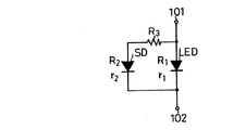
特許文献1の図1には、発光ダイオードのp型GaN層(pクラッド層)の延長部分の抵抗を発光ダイオードのアノード電極とカソード電極との間に接続し、この抵抗を保護素子として使用する別の実施形態が開示されている。発光ダイオードのカソード電極をp型クラッド層の延長部分に接触させると、この接触はショットキー接触又はこれに近い状態になる。従って、特許文献1の保護素子としての抵抗を含む複合半導体装置を図29の等価回路で示すことができる。即ち、この等価回路において、発光ダイオードLEDのアノード電極101とカソード電極102との間にショットキーバリヤダイオードSDが保護用抵抗R3を介して接続されている。保護用抵抗R3はアノード電極101とのショットキーバリヤダイオードSDとの間に介在するp型GaN層(pクラッド層)の長さに比例した値を有する。ショットキーバリヤダイオードSDは発光ダイオードLEDに対して保護用抵抗R3を介して順方向並列接続されている。従って、もし保護用抵抗R3の値が小さいと、発光ダイオードに順方向電圧が印加された時に、保護用抵抗R3を介して電流が流れ、発光ダイオードが発光しない。保護用抵抗R3の値をR3、発光ダイオードLEDの順方向の抵抗値をR1、逆方向の抵抗値をr1、ショットキーバリアダイオードSDの順方向の抵抗値をR2、逆方向の抵抗値をr2とした時、R2+R3がR1よりも十分に大きいことが発光ダイオードLEDの発光条件であり、また、r2+R3がr1よりも十分に小さいことが保護用抵抗R3に基づいて保護機能を得る条件である。
上記条件を満足させるようにp型GaN層(pクラッド層)の延長部分を設定することには困難を伴なう。また、抵抗R3を得るためにpクラッド層の延長部分を設けると、チップサイズが必然的に大きくなる。
特開平10−65215号公報 特開平10−200159号公報
However, when the light emitting diode and the protective pn junction diode are separated and arranged in the lateral direction on the sapphire substrate disclosed in Patent Documents 1 and 2, the composite semiconductor device has the same amount as the protective pn junction diode. Chip size increases. Further, when the chip size is the same as the conventional one, the effective light emitting area of the light emitting diode is reduced, resulting in a decrease in luminance.
Furthermore, if the light emitting diode and the protective pn junction diode are separated and disposed as disclosed in Patent Documents 1 and 2, it is necessary to route a conductor for connecting them in reverse parallel. Only the size of the composite semiconductor device increases.
Further, the protective pn junction diode of Patent Document 1 is configured using an epitaxial growth layer formed simultaneously with the epitaxial growth layer for the light emitting diode. Therefore, the thickness of the semiconductor layer of the protective pn junction diode is limited to the thickness of the epitaxial growth layer of the light emitting diode, and it is difficult to set the forward voltage of the protective pn junction diode to a preferable value. Note that a preferable value of the forward voltage of the protective pn junction diode is higher than the reverse voltage applied to the light emitting diode during normal operation and lower than the allowable maximum reverse voltage of the light emitting diode.
Furthermore, the light-emitting diode according to the embodiment shown in FIG. 8 of Patent Document 1 includes an active layer made of InGaN, a p-type GaN layer (p-clad layer) arranged on one side thereof, and an arrangement on the other side. The protective pn junction diode is composed of an n-type GaN layer, an active layer, the same InGaN layer, and a p-type clad layer, which are continuous with the n-cladding layer. It consists of a GaN layer. The cathode electrode provided on the n-type GaN layer of the protective pn junction diode is connected to the anode electrode of the light emitting diode, and the cathode electrode of the light emitting diode is connected to the n cladding layer. Accordingly, since the cathode electrode of the light emitting diode and the cathode electrode of the protective pn junction diode are both connected to the n-type GaN layer, if the distance between them is short, a current flows between them. There is a possibility that current does not flow through the light emitting diode. For this reason, it is necessary to sufficiently increase the distance between the cathode electrode of the light-emitting diode and the cathode electrode of the protective pn junction diode, which inevitably increases the size of the composite semiconductor device.
In FIG. 1 of Patent Document 1, the resistance of the extended portion of the p-type GaN layer (p clad layer) of the light emitting diode is connected between the anode electrode and the cathode electrode of the light emitting diode, and this resistance is used as a protective element. Another embodiment is disclosed. When the cathode electrode of the light emitting diode is brought into contact with the extended portion of the p-type cladding layer, this contact becomes a Schottky contact or a state close thereto. Therefore, a composite semiconductor device including a resistor as a protection element of Patent Document 1 can be shown by the equivalent circuit of FIG. That is, in this equivalent circuit, the Schottky barrier diode SD is connected between the anode electrode 101 and the cathode electrode 102 of the light emitting diode LED via the protective resistor R3. The protective resistor R3 has a value proportional to the length of the p-type GaN layer (p-cladding layer) interposed between the anode electrode 101 and the Schottky barrier diode SD. The Schottky barrier diode SD is connected in parallel in the forward direction to the light emitting diode LED via a protective resistor R3. Therefore, if the value of the protective resistor R3 is small, when a forward voltage is applied to the light emitting diode, a current flows through the protective resistor R3 and the light emitting diode does not emit light. The value of the protective resistor R3 is R3, the forward resistance value of the light emitting diode LED is R1, the reverse resistance value is r1, the forward resistance value of the Schottky barrier diode SD is R2, and the reverse resistance value is r2. Where R2 + R3 is sufficiently larger than R1 is a light emitting condition of the light emitting diode LED, and r2 + R3 is sufficiently smaller than r1 is a condition for obtaining a protective function based on the protective resistor R3.
It is difficult to set an extension of the p-type GaN layer (p-clad layer) so as to satisfy the above conditions. Further, if an extension portion of the p-clad layer is provided in order to obtain the resistor R3, the chip size is inevitably increased.
JP-A-10-65215 Japanese Patent Laid-Open No. 10-200159

本発明が解決しようとする課題は、保護素子部を伴なった半導体発光装置、即ち発光素子と保護素子との複合半導体装置の小型化を図ることが困難なことである。また、発光素子と受光素子と保護素子との一体化が要求されることがあるが、これ等を含む複合半導体装置の小型化を図ることが困難であった。   The problem to be solved by the present invention is that it is difficult to reduce the size of a semiconductor light emitting device with a protective element portion, that is, a composite semiconductor device of a light emitting element and a protective element. Further, although integration of the light emitting element, the light receiving element, and the protection element may be required, it has been difficult to reduce the size of the composite semiconductor device including these elements.

上記課題を解決するための本発明は、半導体発光素子部とこの半導体発光素子部を過電圧から保護するための保護素子部とを含む複合半導体装置であって、
前記半導体発光素子部は、一方の主面と他方の主面とを有し且つ導電性を有し且つ第1導電型を有する半導体基板と、互いに対向する第1及び第2の主面と前記第1の主面から前記第2の主面に至る傾斜側面とを有し且つ前記第2の主面が前記半導体基板の一方の主面に電気的及び機械的に結合されている発光半導体領域と、前記発光半導体領域の前記第1の主面に配置された第1の電極と、前記半導体基板に接続された第2の電極とを備え、
前記保護素子部は、前記半導体基板の延長部分と前記発光半導体領域の前記傾斜側面に光透過性を有する絶縁膜を介して配置された光透過性を有する第2導電型半導体膜とから成り
前記第2導電型半導体膜の一端部分は前記半導体基板の前記延長部分にpn接合接触し、前記第2導電型半導体膜の他端部分は前記第1の電極に接続され、
前記第1の電極は光透過性を有し、
前記発光半導体領域は前記半導体基板の一方の主面上に気相成長された半導体又は前記半導体基板に熱圧着で貼り合わせた半導体からなることを特徴とする複合半導体装置に係わるものである。
なお、本願において、光とは半導体発光素子部から放射される光を意味する。また、複合半導体装置とは保護素子部を伴なった半導体発光装置を意味する。また、保護素子部とは、半導体発光素子部を過電圧から保護する機能を有する保護素子を意味する。
The present invention for solving the above problems is a composite semiconductor device including a semiconductor light emitting element part and a protective element part for protecting the semiconductor light emitting element part from overvoltage,
The semiconductor light-emitting element section includes a semiconductor substrate having one main surface and the other main surface, having conductivity and having a first conductivity type, first and second main surfaces facing each other, and A light emitting semiconductor region having an inclined side surface extending from the first main surface to the second main surface, wherein the second main surface is electrically and mechanically coupled to one main surface of the semiconductor substrate. A first electrode disposed on the first main surface of the light emitting semiconductor region, and a second electrode connected to the semiconductor substrate,
The protection element portion includes an extended portion of the semiconductor substrate and a light-transmissive second conductive semiconductor film disposed on the inclined side surface of the light-emitting semiconductor region via a light-transmissive insulating film ,
One end portion of the second conductivity type semiconductor film is in pn junction contact with the extension portion of the semiconductor substrate, and the other end portion of the second conductivity type semiconductor film is connected to the first electrode,
The first electrode has optical transparency;
The light-emitting semiconductor region is related to a composite semiconductor device characterized in that it is made of a semiconductor vapor-phase grown on one main surface of the semiconductor substrate or a semiconductor bonded to the semiconductor substrate by thermocompression bonding .
In addition, in this application, light means the light radiated | emitted from a semiconductor light-emitting element part. Further, the composite semiconductor device means a semiconductor light emitting equipment which entailed the protection element portion. Further, the protective element, means a protecting element having a function of protecting the light-emitting portion from an overvoltage.

請求項2に示すように、前記第2導電型半導体膜は前記第1の電極の上を覆う部分を有し、前記覆う部分は前記第1の電極を保護する機能を有していることことが望ましい。前記第2導電型半導体膜の前記覆う部分が耐湿性又は防傷性又はこれらの両方を有する保護膜機能を有することによって、従来の保護膜を省くこと、又は従来の保護膜を保護膜機能の低いものに置き換えることが可能になり、小型化及び低コスト化が可能になる
また、請求項に示すように、第1の電極は、パッド電極機能を有している部分を備えていることが望まし
As shown in claim 2, wherein the second conductive type semiconductor layer has a covering Cormorants upper portion of the first electrode, the covering portion that has a function of protecting the first electrode It is desirable. The covering portion of the second conductive type semiconductor film has a protective film function having moisture resistance or scratch resistance, or both, so that the conventional protective film is omitted or the conventional protective film has a protective film function. it is possible to replace the low, it can be reduced in size and cost.
Further, as shown in claim 3, the first electrode is not to desirable and a part component that has a pad electrode function.

本発明によれば次の効果を得ることができる。
(1) 発光半導体領域をその逆方向又は順方向又はこれ等の両方の過電圧から保護するための前記保護素子部が、前記発光半導体領域の傾斜側面に設けられているので、保護素子部を伴なった半導体発光装置即ち複合半導体装置の小型化を達成することができる。
(2) 導電性を有している基板が使用されているので、基板によって半導体発光素子部と保護素子部との相互接続が容易に達成される。従って、半導体発光素子部と保護素子部との構成が単純化され、小型化及び低コスト化が達成される。
3)第2導電型半導体膜及び絶縁膜が光透過性を有するので、発光半導体領域の傾斜側面から光を外部に取り出すことができ、光の外部取り出し効率が向上する
According to the present invention, the following effects can be obtained.
(1) Since the protective element portion for protecting the light emitting semiconductor region from overvoltages in the reverse direction, the forward direction, or both thereof is provided on the inclined side surface of the light emitting semiconductor region, the protective element portion is provided. It is possible to reduce the size of the semiconductor light emitting device, that is, the composite semiconductor device.
(2) Since the board | substrate which has electroconductivity is used, the interconnection of a semiconductor light-emitting element part and a protection element part is easily achieved by the board | substrate. Therefore, the configuration of the semiconductor light emitting element portion and the protection element portion is simplified, and downsizing and cost reduction are achieved.
( 3) Since the second conductive type semiconductor film and the insulating film are light transmissive, light can be extracted to the outside from the inclined side surface of the light emitting semiconductor region, and the light extraction efficiency is improved .

次に、図1〜図28を参照して本発明の実施形態を説明する。   Next, an embodiment of the present invention will be described with reference to FIGS.

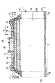
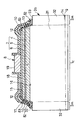
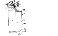
図1に示す本発明の実施例1に従う複合半導体装置は、半導体発光素子部(以下、発光素子部と言う。)1と保護素子部2とから成る。発光素子部1には半導体発光ダイオードが形成され、保護素子部2には発光素子部1を過電圧から保護するための保護ダイオードが形成されている。   The composite semiconductor device according to the first embodiment of the present invention shown in FIG. 1 includes a semiconductor light emitting element portion (hereinafter referred to as a light emitting element portion) 1 and a protection element portion 2. A semiconductor light emitting diode is formed in the light emitting element portion 1, and a protection diode for protecting the light emitting element portion 1 from overvoltage is formed in the protection element portion 2.

発光素子部1と保護素子部2とは共通の導電性基板としてのp型(第1導電型)のシリコン半導体基板3を使用して構成されている。半導体基板3の鎖線で区画して示す中央部分31は主として発光素子の構成に寄与し、中央部分31の延在部分としての外周部分32は主として保護素子の構成に寄与している。この半導体基板3の詳細は後述する。   The light emitting element portion 1 and the protection element portion 2 are configured using a p-type (first conductivity type) silicon semiconductor substrate 3 as a common conductive substrate. A central portion 31 shown by being separated by a chain line of the semiconductor substrate 3 mainly contributes to the configuration of the light emitting element, and an outer peripheral portion 32 as an extending portion of the central portion 31 mainly contributes to the configuration of the protection element. Details of the semiconductor substrate 3 will be described later.

発光素子部1は、半導体基板3の中央部分31と、n型半導体層4、活性層5及びp型半導体層6から成る発光半導体領域(主半導体領域)7と第1の電極8と第2の電極9とから成る。
保護素子部2は、半導体基板3の中央部分31の延在部分としての外周部分32と絶縁膜10と第2導電型半導体膜としてのn型半導体薄膜11とから成る。
第1の電極8の大部分とn型半導体薄膜11は、耐湿性及び防傷性を有する例えばシリコン酸化膜(SiO2)から成る光透過性保護膜12によって覆われている。次に、図1の各部を詳しく説明する。
The light emitting element portion 1 includes a central portion 31 of a semiconductor substrate 3, a light emitting semiconductor region (main semiconductor region) 7 composed of an n-type semiconductor layer 4, an active layer 5 and a p-type semiconductor layer 6, a first electrode 8, and a second electrode. Electrode 9.
The protection element portion 2 includes an outer peripheral portion 32 as an extending portion of the central portion 31 of the semiconductor substrate 3, an insulating film 10, and an n-type semiconductor thin film 11 as a second conductivity type semiconductor film.
Most of the first electrode 8 and the n-type semiconductor thin film 11 are covered with a light-transmitting protective film 12 made of, for example, a silicon oxide film (SiO 2 ) having moisture resistance and scratch resistance. Next, each part of FIG. 1 will be described in detail.

導電性を有する基板としての半導体基板3は導電型決定用不純物としてボロン等の3族元素を含むp型単結晶シリコン基板から成り、一方の主面13と他方の主面14とを有する。この半導体基板3のp型不純物濃度は、例えば5×10¹⁸〜5×1019cm-3程度であり、抵抗率は0.0001Ω・cm〜0.01Ω・cm程度である。従って、半導体基板3は導電性基板であり、発光素子部1の電流通路として機能する。更に、半導体基板3は、発光半導体領域7のエピタキシャル成長のための基板としての機能、及び発光半導体領域7と第1の電極8との機械的支持体としての機能を有する。半導体基板3の好ましい厚みは比較的厚い200〜500μmである。半導体基板3の一方の主面13は平坦であっても差し支えない。しかし、1枚の半導体ウエハから複数の複合半導体装置を作製する時に、比較的大きな面積を有する発光半導体領域7を図3に示すようにエッチングによって複数個に分割すると、必然的に半導体基板3もエッチングされて凹部即ち段部33が生じる。このエッチングにおいて、半導体基板3は発光半導体領域7をエッチングストッパとして機能している。なお、保護素子部2の複合化の有無に関係なく、ウエハを個別の半導体発光素子に分割する時に、2つの発光半導体領域の相互間に分割のために必要な幅(w+w)を有する段部33又は発光半導体領域7で覆われない部分が生じる。 The semiconductor substrate 3 as a conductive substrate is made of a p-type single crystal silicon substrate containing a Group 3 element such as boron as an impurity for determining the conductivity type, and has one main surface 13 and the other main surface 14. The semiconductor substrate 3 has a p-type impurity concentration of, for example, about 5 × 10 18 to 5 × 10 19 cm −3 and a resistivity of about 0.0001 Ω · cm to 0.01 Ω · cm. Therefore, the semiconductor substrate 3 is a conductive substrate and functions as a current path of the light emitting element portion 1. Further, the semiconductor substrate 3 has a function as a substrate for epitaxial growth of the light emitting semiconductor region 7 and a function as a mechanical support for the light emitting semiconductor region 7 and the first electrode 8. A preferable thickness of the semiconductor substrate 3 is 200 to 500 μm, which is relatively thick. One main surface 13 of the semiconductor substrate 3 may be flat. However, when manufacturing a plurality of composite semiconductor devices from one semiconductor wafer, if the light emitting semiconductor region 7 having a relatively large area is divided into a plurality of parts by etching as shown in FIG. Etching produces a recess or step 33. In this etching, the semiconductor substrate 3 functions as a light emitting semiconductor region 7 as an etching stopper. Note that, when the wafer is divided into individual semiconductor light emitting elements regardless of whether the protection element portion 2 is combined, a step portion having a width (w + w) necessary for the division between the two light emitting semiconductor regions. 33 or a portion not covered with the light emitting semiconductor region 7 is generated.

半導体基板3上には、一般にn型クラッド層と呼ばれているn型半導体層4と活性層5と一般にp型クラッド層と呼ばれているp型半導体層6とが順次に周知のエピタキシャル成長法によって形成されている。発光半導体領域7の各層4、5、6は3−5族化合物半導体の1種である周知の窒化物半導体から成る。従って、発光半導体領域7のn型半導体層4とシリコン半導体基板3とはヘテロ接合である。図1ではp型半導体基板3に対してn型半導体層4が接触しているが、これらのヘテロ接合界面の電圧降下は比較的小さい。即ち、p型シリコン半導体基板3と窒化物半導体から成るn型半導体層4との間に図示されていない合金化層が生じているために、第1及び第2の電極8、9間に発光半導体領域7を順方向バイアスする向きの電圧を印加した時のn型半導体層4とp型半導体基板3との間の界面における電圧降下は小さい。勿論、図1のp型半導体基板3の代りにn型半導体基板を使用し、且つn型半導体薄膜11の代りにp型半導体薄膜を形成することもできる。   On the semiconductor substrate 3, an n-type semiconductor layer 4 generally called an n-type cladding layer, an active layer 5, and a p-type semiconductor layer 6 generally called a p-type cladding layer are sequentially formed by a known epitaxial growth method. Is formed by. Each layer 4, 5, 6 of the light emitting semiconductor region 7 is made of a well-known nitride semiconductor which is a kind of group 3-5 compound semiconductor. Therefore, the n-type semiconductor layer 4 in the light emitting semiconductor region 7 and the silicon semiconductor substrate 3 are heterojunctions. In FIG. 1, the n-type semiconductor layer 4 is in contact with the p-type semiconductor substrate 3, but the voltage drop at these heterojunction interfaces is relatively small. That is, since an alloyed layer (not shown) is formed between the p-type silicon semiconductor substrate 3 and the n-type semiconductor layer 4 made of a nitride semiconductor, light is emitted between the first and second electrodes 8 and 9. The voltage drop at the interface between the n-type semiconductor layer 4 and the p-type semiconductor substrate 3 when a voltage in a direction for forward biasing the semiconductor region 7 is applied is small. Of course, an n-type semiconductor substrate can be used in place of the p-type semiconductor substrate 3 in FIG. 1 and a p-type semiconductor thin film can be formed in place of the n-type semiconductor thin film 11.

n型半導体層4は、図1において1つの層で示されているが、バッファ層とn型半導体層との組み合せで構成することができる。
図1において活性層5も1つの層で示されているが、実際には周知の多重量子井戸構造を有している。もし、ダブルヘテロ接合構造にすることが要求されない場合には、発光半導体領域7から活性層5を省くこともできる。
図1において、活性層5の上に配置されたp型半導体層6は1つの層で示されているが、このp型半導体層6に周知の電流拡散層、コンタクト層等を含めることができる。
Although the n-type semiconductor layer 4 is shown as one layer in FIG. 1, it can be configured by a combination of a buffer layer and an n-type semiconductor layer.
In FIG. 1, the active layer 5 is also shown as a single layer, but actually has a well-known multiple quantum well structure. If the double heterojunction structure is not required, the active layer 5 can be omitted from the light emitting semiconductor region 7.
In FIG. 1, the p-type semiconductor layer 6 disposed on the active layer 5 is shown as a single layer. However, the p-type semiconductor layer 6 can include a known current diffusion layer, contact layer, and the like. .

発光半導体領域7は、互いに対向している第1及び第2の主面15、16と、傾斜を有する側面17とを有している。この実施例1では発光半導体領域7の第1の主面15が光取出しに利用され、第2の主面16が半導体基板3の一方の主面13に電気的及び機械的に結合されている。
なお、この実施例1では図2に示すように発光半導体領域7及び半導体基板3が平面的に見て四角形のパターンを有しているが、それぞれを平面的に見て円形パターン又は別の任意のパターンとすることができる。また、半導体基板3を四角形パターンとし、発光半導体領域7のみを円形パターン又は任意のパターンとすることもできる。
The light emitting semiconductor region 7 has first and second main surfaces 15 and 16 that face each other, and an inclined side surface 17. In the first embodiment, the first main surface 15 of the light emitting semiconductor region 7 is used for light extraction, and the second main surface 16 is electrically and mechanically coupled to one main surface 13 of the semiconductor substrate 3. .
In the first embodiment, as shown in FIG. 2, the light emitting semiconductor region 7 and the semiconductor substrate 3 have a quadrangular pattern when seen in a plan view. Pattern. Alternatively, the semiconductor substrate 3 may be a rectangular pattern, and only the light emitting semiconductor region 7 may be a circular pattern or an arbitrary pattern.

発光半導体領域7の上に配置された第1の電極8は、第1の部分としての光透過性電極18と第2の部分としてのボンディングパッド電極19とから成る。光透過性電極18は発光半導体領域7の第1の主面15のほぼ全体に配置され、且つp型半導体層6に電気的に接続されている。この光透過性電極18は、一般にITOと呼ばれている酸化インジュム(In23)と酸化錫(SnO2 )との混合物から成る100nm程度の膜とすることが望ましい。しかし、光透過性電極18をITO以外のZnO(酸化亜鉛)、Ag(銀)等の別の材料で光透過可能な厚みに形成することもできる。ボンディングパッド電極19は発光半導体領域7の第1の主面15の面積よりも小さい面積を有するように形成され且つAl又はAu等から成る外部接続用ワイヤを結合することができる金属からなり、光透過性電極18に接続されている。このボンディングパッド電極19は光透過性電極18よりも厚く形成され且つ光を実質的に透過させないので、図2で鎖線で示すように発光半導体領域7の第1の主面15の中央部分に限定的に配置されている。 The first electrode 8 disposed on the light emitting semiconductor region 7 includes a light transmissive electrode 18 as a first portion and a bonding pad electrode 19 as a second portion. The light transmissive electrode 18 is disposed on almost the entire first main surface 15 of the light emitting semiconductor region 7 and is electrically connected to the p-type semiconductor layer 6. The light transmissive electrode 18 is preferably a film having a thickness of about 100 nm made of a mixture of indium oxide (In 2 O 3 ) and tin oxide (SnO 2 ), generally called ITO. However, it is also possible to form the light transmissive electrode 18 with a thickness that allows light transmission with another material such as ZnO (zinc oxide) or Ag (silver) other than ITO. The bonding pad electrode 19 is formed of a metal which is formed to have an area smaller than the area of the first main surface 15 of the light emitting semiconductor region 7 and can be coupled with an external connection wire made of Al, Au, or the like. The transparent electrode 18 is connected. Since this bonding pad electrode 19 is formed thicker than the light transmissive electrode 18 and does not substantially transmit light, it is limited to the central portion of the first main surface 15 of the light emitting semiconductor region 7 as shown by a chain line in FIG. Are arranged.

第2の電極9は半導体基板3の他方の主面14に接続されている。なお、半導体基板3は導電性を有するので、第2の電極9を半導体基板3の一方の主面13の外周部分に接続することもできる。   The second electrode 9 is connected to the other main surface 14 of the semiconductor substrate 3. Since the semiconductor substrate 3 has conductivity, the second electrode 9 can be connected to the outer peripheral portion of one main surface 13 of the semiconductor substrate 3.

発光半導体領域7を静電気等の過電圧から保護するための保護素子部2の一部としてのn型半導体薄膜11は、p型の半導体基板3の外周部分32にpn接触している一端部分と、絶縁膜10を介して発光半導体領域7の側面17上に配置されている部分と、第1の電極8の一部である光透過性電極18に電気的に接続されている他端部分とを有する。このn型半導体薄膜11とp型の半導体基板3との界面のpn接合が保護ダイオードとして機能する。発光半導体領域7の側面17が傾斜しているために、平面的に見て即ち半導体基板3の一方の主面13に対して垂直な方向から半導体基板3を見て、保護素子部2の一部としてのn型半導体薄膜11が半導体基板3の内側に配置されている。
この実施例1では、傾斜している側面17からの光取出しを可能にするために、絶縁膜10は1nm〜2nm程度に形成され、またn型半導体薄膜11も1nm〜2nm程度に形成され、それぞれが光透過性を有する。また、n型半導体薄膜11と光透過性電極18とを覆う保護膜12も光透過性を有する材料及び厚さに形成されている。n型半導体薄膜11に光透過性が要求されないか、又は光透過性が低くても差し支えない場合は、n型半導体薄膜11の厚みを1nm〜1μmの範囲で任意に変えること、又はn型半導体薄膜11を1μmよりも厚いn型半導体厚膜に変えることができる。
The n-type semiconductor thin film 11 as a part of the protection element portion 2 for protecting the light emitting semiconductor region 7 from an overvoltage such as static electricity has one end portion in pn contact with the outer peripheral portion 32 of the p-type semiconductor substrate 3, A portion disposed on the side surface 17 of the light emitting semiconductor region 7 through the insulating film 10 and the other end portion electrically connected to the light transmissive electrode 18 which is a part of the first electrode 8 Have. The pn junction at the interface between the n-type semiconductor thin film 11 and the p-type semiconductor substrate 3 functions as a protective diode. Since the side surface 17 of the light emitting semiconductor region 7 is inclined, when the semiconductor substrate 3 is viewed from a direction perpendicular to the one main surface 13 of the semiconductor substrate 3, An n-type semiconductor thin film 11 as a part is disposed inside the semiconductor substrate 3.
In Example 1, in order to enable light extraction from the inclined side surface 17, the insulating film 10 is formed to about 1 nm to 2 nm, and the n-type semiconductor thin film 11 is also formed to about 1 nm to 2 nm. Each is light transmissive. Further, the protective film 12 covering the n-type semiconductor thin film 11 and the light transmissive electrode 18 is also formed with a material and thickness having light transmissive properties. If the n-type semiconductor thin film 11 is not required to have light transmission or may have low light transmission, the thickness of the n-type semiconductor thin film 11 is arbitrarily changed within the range of 1 nm to 1 μm, or the n-type semiconductor The thin film 11 can be changed to an n-type semiconductor thick film thicker than 1 μm.

図1のn型半導体薄膜11はアモルファス(非晶質)シリコンで形成されているが、この代りに例えばITO、ZnO、SnO2 、In23、ZnS、ZnSe、ZnSb26、CdO、CdIn24 、MgIn24 、ZnGa24 、CdGa24、Ga23、GaIn3 、CdSnO4 、InGaMgO4 、InGasZnO4 、Zn2In25 、AgSbO3 、Cd2Sb27、Cd2GeO4 、AgInO2、CdS、CdSe等で形成することもできる。また、n型半導体薄膜11の代わりにn型半導体厚膜を設けることもできる。
半導体薄膜11は、蒸着、又はCVD、又は印刷(塗布)、又はスパッタ等の周知の方法で形成される。
The n-type semiconductor thin film 11 shown in FIG. 1 is formed of amorphous (amorphous) silicon. Instead, for example, ITO, ZnO, SnO 2 , In 2 O 3 , ZnS, ZnSe, ZnSb 2 O 6 , CdO, CdIn 2 O 4 , MgIn 2 O 4 , ZnGa 2 O 4 , CdGa 2 O 4 , Ga 2 O 3 , GaIn 3 , CdSnO 4 , InGaMgO 4 , InGasZnO 4 , Zn 2 In 2 O 5 , AgSbO 3 , Cd 2 Sb It can also be formed of 2 O 7 , Cd 2 GeO 4 , AgInO 2 , CdS, CdSe, or the like. Further, an n-type semiconductor thick film can be provided instead of the n-type semiconductor thin film 11.
The semiconductor thin film 11 is formed by a known method such as vapor deposition, CVD, printing (application), or sputtering.

この実施例では発光半導体領域7の側面17の全周を囲むようにn型半導体薄膜11が形成されているが、側面17の一部のみに半導体薄膜11を形成することもできる。しかし、側面17の全周又はできるだけ多くの部分に半導体薄膜11を形成することが望ましい。これにより、n型半導体薄膜11を薄く形成しても、所望の電流容量を得ることが可能になる。   In this embodiment, the n-type semiconductor thin film 11 is formed so as to surround the entire periphery of the side surface 17 of the light emitting semiconductor region 7. However, the semiconductor thin film 11 can be formed only on a part of the side surface 17. However, it is desirable to form the semiconductor thin film 11 on the entire circumference of the side surface 17 or as much as possible. Thereby, even if the n-type semiconductor thin film 11 is formed thin, a desired current capacity can be obtained.

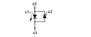
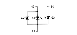
図1の複合半導体装置の発光素子部1は図4の発光素子としての発光ダイオード41の機能を有し、保護素子部2は図4の保護素子としての保護ダイオード42の機能を有する。図1の第1及び第2の電極8、9は図4の第1及び第2の端子43、44として機能する。従って、発光素子部1に基づく発光ダイオード41に対して保護素子部2に基づく保護ダイオード42は逆方向並列に接続されている。   1 has the function of the light emitting diode 41 as the light emitting element of FIG. 4, and the protection element portion 2 has the function of the protection diode 42 as the protection element of FIG. The first and second electrodes 8 and 9 in FIG. 1 function as the first and second terminals 43 and 44 in FIG. Therefore, the protection diode 42 based on the protection element portion 2 is connected in reverse direction parallel to the light emitting diode 41 based on the light emitting element portion 1.

保護ダイオード42の順方向電圧即ち順方向の立上り電圧(導通開始電圧)は、発光ダイオード41の許容最大逆方向電圧(逆方向耐電圧)よりも低く設定される。また、保護ダイオード42の順方向電圧は、正常時に発光ダイオード41に印加される逆方向電圧よりも高いことが望ましい。発光ダイオード41に異常な逆方向の電圧が印加されると、保護ダイオード42が導通し、発光ダイオード41の電圧が保護ダイオード42の順方向電圧に抑えられ、発光ダイオード41に逆方向のサージ電圧等の過電圧が印加されることを阻止でき、発光ダイオード41を破壊から保護することができる。
なお、保護ダイオード42をツエナーダイオード等の定電圧ダイオードで構成することもできる。この定電圧ダイオードの逆方向の降伏電圧は、発光ダイオード41に対して正常時に順方向に印加される電圧と許容最大順方向電圧(順方向耐電圧)との間であることが望ましい。これにより、定電圧ダイオードの逆方向降伏電圧以上の電圧が発光ダイオード41に印加されることを防ぐことができ、発光ダイオード41をサージ電圧等の順方向の過電圧から保護することができる。定電圧ダイオードの順方向電圧は保護ダイオード42の順方向電圧と同一であることが望ましい。
定電圧ダイオードを設けると、発光ダイオード41を逆方向と順方向との両方の過電圧から保護することができる。もし、発光ダイオード41を逆方向の過電圧から保護することが要求されない場合は、定電圧ダイオードの順方向電圧を任意に設定し、定電圧ダイオードによって発光ダイオード41を順方向の過電圧から保護する。
The forward voltage of the protection diode 42, that is, the rising voltage in the forward direction (conduction start voltage) is set lower than the allowable maximum reverse voltage (reverse withstand voltage) of the light emitting diode 41. Further, it is desirable that the forward voltage of the protection diode 42 is higher than the reverse voltage applied to the light emitting diode 41 during normal operation. When an abnormal reverse voltage is applied to the light emitting diode 41, the protective diode 42 is turned on, the voltage of the light emitting diode 41 is suppressed to the forward voltage of the protective diode 42, and a reverse surge voltage or the like is applied to the light emitting diode 41. It is possible to prevent the overvoltage from being applied, and to protect the light emitting diode 41 from destruction.
Note that the protective diode 42 may be a constant voltage diode such as a Zener diode. The breakdown voltage in the reverse direction of the constant voltage diode is preferably between a voltage applied in the forward direction to the light emitting diode 41 in a normal state and an allowable maximum forward voltage (forward withstand voltage). As a result, it is possible to prevent a voltage higher than the reverse breakdown voltage of the constant voltage diode from being applied to the light emitting diode 41, and to protect the light emitting diode 41 from forward overvoltage such as surge voltage. The forward voltage of the constant voltage diode is preferably the same as the forward voltage of the protection diode 42.
When the constant voltage diode is provided, the light emitting diode 41 can be protected from overvoltage in both the reverse direction and the forward direction. If it is not required to protect the light emitting diode 41 from reverse overvoltage, the forward voltage of the constant voltage diode is arbitrarily set, and the light emitting diode 41 is protected from forward overvoltage by the constant voltage diode.

本実施例の複合半導体装置は次の効果を有する。
(1) 発光半導体領域7の側面17上に保護素子部2の一部を配置し、且つ発光半導体領域7が設けられない半導体基板3の外周部分32を保護素子部2の一部として使用する構成であるので、半導体基板3の一方の主面13に対する発光半導体領域7の占有面積の実質的な低減を伴なわないで過電圧保護機能を得ることができる。要するに、従来と同一の光出力を得る場合には、複合半導体装置の小型化を達成することができる。また、複合半導体装置を従来と同一寸法に形成する場合には、従来よりも光出力を大きくすることができる。
(2) 発光半導体領域7の側面17が傾斜しているので、平面的に見て保護素子部2の一部としてのn型半導体薄膜11を半導体基板3の内側に配置することができ、複合半導体装置の小型化を良好に達成することができる。
(3) 発光素子部1と保護素子部2とで共通の半導体基板3を使用し、且つn型半導体薄膜11を第1の電極8に直接に接続する構成であるので、図4に示すように発光ダイオード41に保護ダイオード42を並列接続する構成及び工程を簡略化することができ、複合半導体装置の小型化及び低コスト化を達成することができる。
(4) n型半導体薄膜11を、生産性に優れた蒸着、CVD、スパッタ、スクリーン印刷等で形成できるので、保護素子の製造コストの低減を図ることができる。
(5) 絶縁膜10、n型半導体薄膜11、保護膜12が光透過性を有するので、発光半導体領域7の側面17から光を外部に取り出すことができ、光の外部取り出し効率が向上する。
The composite semiconductor device of this embodiment has the following effects.
(1) A part of the protective element portion 2 is arranged on the side surface 17 of the light emitting semiconductor region 7, and the outer peripheral portion 32 of the semiconductor substrate 3 where the light emitting semiconductor region 7 is not provided is used as a part of the protective element portion 2. Due to the configuration, an overvoltage protection function can be obtained without substantially reducing the area occupied by the light emitting semiconductor region 7 with respect to the one main surface 13 of the semiconductor substrate 3. In short, in the case of obtaining the same optical output as before, it is possible to reduce the size of the composite semiconductor device. Further, when the composite semiconductor device is formed with the same dimensions as the conventional one, the light output can be increased as compared with the conventional one.
(2) Since the side surface 17 of the light emitting semiconductor region 7 is inclined, the n-type semiconductor thin film 11 as a part of the protection element portion 2 can be disposed inside the semiconductor substrate 3 in a plan view, and the composite Miniaturization of the semiconductor device can be achieved satisfactorily.
(3) Since the light emitting element unit 1 and the protection element unit 2 use the common semiconductor substrate 3 and the n-type semiconductor thin film 11 is directly connected to the first electrode 8, as shown in FIG. In addition, the configuration and process of connecting the protective diode 42 to the light emitting diode 41 in parallel can be simplified, and the size and cost of the composite semiconductor device can be reduced.
(4) Since the n-type semiconductor thin film 11 can be formed by vapor deposition, CVD, sputtering, screen printing or the like with excellent productivity, the manufacturing cost of the protective element can be reduced.
(5) Since the insulating film 10, the n-type semiconductor thin film 11, and the protective film 12 are light transmissive, light can be extracted to the outside from the side surface 17 of the light emitting semiconductor region 7, and the light extraction efficiency is improved.

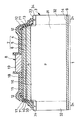
図5に示す実施例2に従う複合半導体装置は、変形した保護素子部2aを設け、この他は図1と同一に構成したものである。従って、図5、及び後述する図6〜図28において図1と実質的に同一の部分には同一の符号を付し、また、図5〜図28において相互に共通する部分には同一の符号を付し、その説明を省略する。   The composite semiconductor device according to the second embodiment shown in FIG. 5 is provided with a modified protection element portion 2a, and the other configuration is the same as that of FIG. Therefore, in FIG. 5 and FIGS. 6 to 28 to be described later, substantially the same parts as in FIG. 1 are denoted by the same reference numerals, and in FIGS. The description is omitted.

図5の保護素子部2aは、図1の保護素子部2から絶縁膜10を省き、この他は図1と同一に形成したものに相当する。絶縁膜10が省かれているので、図5ではn型半導体薄膜11が発光半導体領域7の側面17に直接に接触している。しかし、n型半導体薄膜11を活性層5よりも大きなバンドギャップを有する材料、好ましくは発光半導体領域7の各層4、5、6よりも大きなバンドギャップを有する材料で形成することによってn型半導体薄膜11から発光半導体領域7へ又はこの逆のリーク電流は極めて小さくなり、実用上問題がない。
従って、図5の実施例によっても図1の実施例と同一の効果を得ることができる。
The protective element portion 2a of FIG. 5 corresponds to the protective element portion 2a of FIG. 1 except that the insulating film 10 is omitted and the other portions are the same as those of FIG. Since the insulating film 10 is omitted, the n-type semiconductor thin film 11 is in direct contact with the side surface 17 of the light emitting semiconductor region 7 in FIG. However, the n-type semiconductor thin film 11 is formed of a material having a larger band gap than the active layer 5, preferably a material having a larger band gap than the layers 4, 5, 6 of the light emitting semiconductor region 7. The leakage current from 11 to the light emitting semiconductor region 7 or vice versa is extremely small, and there is no practical problem.
Therefore, the same effect as the embodiment of FIG. 1 can be obtained also by the embodiment of FIG.

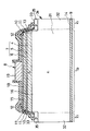
図6に示す実施例3の複合半導体装置は、変形された保護素子部2bを設けた他は図1と同一に形成したものである。   The composite semiconductor device of Example 3 shown in FIG. 6 is formed in the same manner as FIG. 1 except that a modified protection element portion 2b is provided.

図6の保護素子部2bは光透過性電極18と同一材料(例えばITO)から成るn型半導体薄膜11aを設け、この他は図1と同一に構成したものである。図6のn型半導体薄膜11aは光透過性電極18と同一材料であるので、両者を同一工程で形成し、連続させることができる。これにより、複合半導体装置の製造工程の簡略化を図ることができる。なお、光透過性電極18がn型半導体薄膜であっても、p型半導体層6との間の障壁はさほど高くないので実用上問題ない。
本実施例3は上記効果の他に図1の実施例1と同一の効果も有する。
6 is provided with an n-type semiconductor thin film 11a made of the same material (for example, ITO) as the light transmissive electrode 18, and the other configuration is the same as that of FIG. Since the n-type semiconductor thin film 11a of FIG. 6 is made of the same material as the light-transmitting electrode 18, both can be formed in the same process and can be made continuous. Thereby, the manufacturing process of the composite semiconductor device can be simplified. Even if the light transmissive electrode 18 is an n-type semiconductor thin film, there is no practical problem because the barrier to the p-type semiconductor layer 6 is not so high.
The third embodiment has the same effect as the first embodiment shown in FIG.

図6の変形として図6を図5と同様に絶縁膜10を省き、n型半導体薄膜11を発光半導体領域7の側面17に直接に形成することもできる。   As a modification of FIG. 6, the insulating film 10 can be omitted from FIG. 6 similarly to FIG. 5, and the n-type semiconductor thin film 11 can be formed directly on the side surface 17 of the light emitting semiconductor region 7.

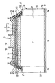
図7の実施例4の複合半導体装置は、変形された発光素子部1a及び保護素子部2cを設けた他は図1と同一に形成したものである。
変形された発光素子部1aは図1の保護膜12の代りに光透過性を有するn型半導体薄膜11の延在部分12aを光透過性電極15の上に配置し、この他は図1と同一に形成したものに相当する。図7の保護素子部2cは図1の保護素子部2から保護膜17を省き、この他は図1と同一に形成したものに相当する。
The composite semiconductor device of Example 4 in FIG. 7 is formed in the same manner as in FIG. 1 except that a modified light emitting element portion 1a and protective element portion 2c are provided.
In the modified light emitting element portion 1a, the extended portion 12a of the light-transmitting n-type semiconductor thin film 11 is disposed on the light transmitting electrode 15 instead of the protective film 12 of FIG. It corresponds to the same formed. The protective element portion 2c of FIG. 7 corresponds to the protective element portion 2 of FIG. 1 except that the protective film 17 is omitted, and the other portions are the same as those of FIG.

この実施例4では、n型半導体薄膜11の延在部分12aが光透過性電極15の保護膜として機能しているので、保護膜の形成を省くことができ、この分だけコストの低減を図ることができる。
なお、図7の実施例4は図1の実施例1と同一の効果も有する。
In Example 4, since the extended portion 12a of the n-type semiconductor thin film 11 functions as a protective film for the light transmissive electrode 15, the formation of the protective film can be omitted, and the cost can be reduced accordingly. be able to.
In addition, Example 4 of FIG. 7 has the same effect as Example 1 of FIG.

図8の実施例5の複合半導体装置は、変形された保護素子部2dを設け、この他は図1と同一に形成したものである。   The composite semiconductor device of Example 5 in FIG. 8 is provided with a modified protection element portion 2d, and the other components are formed in the same manner as in FIG.

図8の保護素子部2dは図1の保護素子部2にp型半導体薄膜50を追加し、この他は図1と実質的に同一に形成したものである。図8のp型(第1導電型)半導体薄膜50はp型の半導体基板3の外周部分32に低抵抗接触して電気的に接続されている一端部分と絶縁膜10を介して発光半導体領域7の側面17に対向配置されている部分とを有する。n型(第2導電型)半導体薄膜11はp型半導体薄膜50にpn接触している一端部分と絶縁膜10を介して発光半導体領域7の側面17に対向配置されている部分と光透過性電極15に低抵抗接触して電気的に接続されている他端部分とを有する。保護膜12はp型半導体薄膜50とn型半導体薄膜11との両方を被覆している。
なお、p型半導体薄膜50は、アモルファスシリコン、NiO、Cu2 O、FeO、CuAlO2、CuGaO2、SrCu22等で形成することができる。
The protection element portion 2d of FIG. 8 is obtained by adding a p-type semiconductor thin film 50 to the protection element portion 2 of FIG. A p-type (first conductivity type) semiconductor thin film 50 in FIG. 8 is a light-emitting semiconductor region through an insulating film 10 and one end portion electrically connected to the outer peripheral portion 32 of the p-type semiconductor substrate 3 in low resistance contact. 7 and a portion disposed opposite to the side surface 17. The n-type (second conductivity type) semiconductor thin film 11 is light-transmissive with one end portion in pn contact with the p-type semiconductor thin film 50 and a portion disposed opposite to the side surface 17 of the light emitting semiconductor region 7 with the insulating film 10 interposed therebetween. And the other end portion electrically connected to the electrode 15 with low resistance. The protective film 12 covers both the p-type semiconductor thin film 50 and the n-type semiconductor thin film 11.
The p-type semiconductor thin film 50 can be formed of amorphous silicon, NiO, Cu 2 O, FeO, CuAlO 2 , CuGaO 2 , SrCu 2 O 2 or the like.

図8の実施例5ではp型半導体薄膜50とn型半導体薄膜11との間のpn接合が図4の保護ダイオード42と同様に機能する。   In Example 5 of FIG. 8, the pn junction between the p-type semiconductor thin film 50 and the n-type semiconductor thin film 11 functions similarly to the protection diode 42 of FIG.

なお、図8の実施例5においても、図5と同様に絶縁膜10を省くこと、図6と同様にn型半導体薄膜11を光透過性電極15と同一材料で形成すること、図7と同様にn型半導体薄膜11を光透過性電極15の上に延在させて保護膜12を省くことができる。   Also in Example 5 of FIG. 8, the insulating film 10 is omitted as in FIG. 5, the n-type semiconductor thin film 11 is formed of the same material as the light transmissive electrode 15 as in FIG. 6, and FIG. Similarly, the protective film 12 can be omitted by extending the n-type semiconductor thin film 11 on the light transmissive electrode 15.

図9の実施例6の複合半導体装置は、変形された発光素子部1bと保護素子部2eを設け、その他は図1と同一に形成したものである。従って、図9において図1と同一の部分には同一の符号を付してその説明を省略する。   The composite semiconductor device of Example 6 in FIG. 9 is provided with a modified light emitting element portion 1b and protective element portion 2e, and the others are formed in the same manner as in FIG. Therefore, in FIG. 9, the same parts as those in FIG.

図9の発光素子部1bはn型シリコン半導体基板3aを有する他は図1と同一に形成されている。図9の保護素子部2eは図8と同様にp型半導体薄膜50を有し、更に金属層51を有する。金属層51は半導体基板3の外周部分32の一方の主面13上に配置された部分と絶縁膜10を介して発光半導体領域7の側面17に対向配置されている部分とを有する。   The light emitting element portion 1b of FIG. 9 is formed in the same manner as FIG. 1 except that it includes an n-type silicon semiconductor substrate 3a. 9 includes a p-type semiconductor thin film 50 and a metal layer 51 as in FIG. The metal layer 51 has a portion disposed on one main surface 13 of the outer peripheral portion 32 of the semiconductor substrate 3 and a portion disposed to face the side surface 17 of the light emitting semiconductor region 7 with the insulating film 10 interposed therebetween.

p型半導体薄膜50は絶縁膜10を介して発光半導体領域7の側面17に対向配置されている部分と金属層51に低抵抗接触して電気的に接続されている部分とを有する。図9のn型半導体薄膜11は図8と同様にp型半導体薄膜50にpn接触している部分と光透過性電極18に低抵抗接触して電気的に接続されている部分とを有する。   The p-type semiconductor thin film 50 has a portion disposed opposite to the side surface 17 of the light emitting semiconductor region 7 through the insulating film 10 and a portion electrically connected to the metal layer 51 in low resistance contact. The n-type semiconductor thin film 11 of FIG. 9 has a portion that is in pn contact with the p-type semiconductor thin film 50 and a portion that is electrically connected in low-resistance contact with the light transmissive electrode 18 as in FIG.

図9の実施例6は図8の実施例5に金属層51を追加した点を除いて図8と実質的に同一に構成したものであるので、実施例5と同一の効果を有する。
なお、図9では金属層51を有するので、n型半導体基板3aが使用されている。しかし、図9では半導体基板3aの導電型がp型半導体薄膜50に拘束されないので、半導体基板3aの導電型をp型に変えることもできる。
The sixth embodiment of FIG. 9 has substantially the same effect as that of the fifth embodiment except that the metal layer 51 is added to the fifth embodiment of FIG.
In FIG. 9, since the metal layer 51 is provided, the n-type semiconductor substrate 3a is used. However, in FIG. 9, since the conductivity type of the semiconductor substrate 3a is not constrained by the p-type semiconductor thin film 50, the conductivity type of the semiconductor substrate 3a can be changed to the p-type.

図9の実施例6においても、図5と同様に絶縁膜10を省くこと、図6と同様にn型半導体薄膜11を光透過性電極18と同一材料で形成すること、図7と同様にn型半導体薄膜11を光透過性電極18の上に延在させて保護膜12を省くことができる。   Also in Example 6 of FIG. 9, the insulating film 10 is omitted as in FIG. 5, the n-type semiconductor thin film 11 is formed of the same material as the light transmissive electrode 18 as in FIG. 6, and as in FIG. The protective film 12 can be omitted by extending the n-type semiconductor thin film 11 on the light transmissive electrode 18.

図10の実施例7の複合半導体装置は、変形された発光素子部1bと保護素子部2fを設け、この他は図1と同一に形成したものである。   The composite semiconductor device of Example 7 in FIG. 10 is provided with a modified light emitting element portion 1b and a protective element portion 2f, and the others are formed in the same manner as in FIG.

図10の発光素子部1bはn型シリコン半導体基板3aを有する他は図1と同一に形成されている。図10の保護素子部2fは、n型の第1の半導体薄膜61とp型の第2の半導体薄膜62とn型の第3の半導体薄膜63とを有する。n型の第1の半導体薄膜61はn型の半導体基板3aに接触している部分と発光半導体領域7の側面17上に絶縁膜10を介して配置されている部分とを有する。n型の第1及び第3の半導体薄膜61、63は、図1のn型半導体薄膜11と同一材料によって同一方法で形成されている。p型の第2の半導体薄膜62はn型の第1の半導体薄膜61にpn接触している部分と絶縁膜10を介して発光半導体領域7の側面17上に配置された部分とを有する。このp型の第2の半導体薄膜62は図8及び図9に示されているp型半導体薄膜50と同一材料によって同一方法で形成されている。n型の第3の半導体薄膜63はp型の第2の半導体薄膜62にpn接触している部分と光透過性電極18に接続されている部分とを有する。第1、第2及び第3の半導体薄膜61、62、63は発光半導体領域7の側面17に対向配置された部分を有し且つ互いに重ねられた部分を有してnpn3層ダイオードを構成している。   The light emitting element portion 1b of FIG. 10 is formed in the same manner as FIG. 1 except that it includes an n-type silicon semiconductor substrate 3a. 10 includes an n-type first semiconductor thin film 61, a p-type second semiconductor thin film 62, and an n-type third semiconductor thin film 63. The n-type first semiconductor thin film 61 has a portion that is in contact with the n-type semiconductor substrate 3 a and a portion that is disposed on the side surface 17 of the light emitting semiconductor region 7 with the insulating film 10 interposed therebetween. The n-type first and third semiconductor thin films 61 and 63 are formed of the same material and by the same method as the n-type semiconductor thin film 11 of FIG. The p-type second semiconductor thin film 62 has a portion in pn contact with the n-type first semiconductor thin film 61 and a portion disposed on the side surface 17 of the light emitting semiconductor region 7 with the insulating film 10 interposed therebetween. The p-type second semiconductor thin film 62 is formed of the same material and by the same method as the p-type semiconductor thin film 50 shown in FIGS. The n-type third semiconductor thin film 63 has a portion in pn contact with the p-type second semiconductor thin film 62 and a portion connected to the light transmissive electrode 18. The first, second, and third semiconductor thin films 61, 62, and 63 have a portion disposed opposite to the side surface 17 of the light emitting semiconductor region 7 and have a portion overlapped with each other to form an npn three-layer diode. Yes.

図10の複合半導体装置の等価回路を図11で示すことができる。図11の発光素子としての発光ダイオード41は発光素子部1bに対応し、保護素子としてのnpn3層ダイオード42aは保護素子部2fに対応し、第1の端子43は第1の電極8に対応し、第2の端子44は第2の電極9に対応している。発光ダイオード41に並列接続されたnpn3層ダイオード42aは、一般にダイアック(DIAC)又は双方向性ダイオードと呼ばれるものであって、逆方向に接続された第1のダイオードD1 と順方向に接続された第2のダイオードD2 との直列回路で示すことができる。なおnpn3層ダイオード42aを逆方向の第1のダイオードD1 と順方向の第2のダイオードD2 との並列回路で示すこともある。npn3層ダイオード42aの順方向及び逆方向の降伏電圧は図4に関係して説明した定電圧ダイオードと同様に設定される。即ち、npn3層ダイオード42aに第2の端子44から第1の端子43に向う逆方向の電圧が印加された時の降伏電圧は、発光ダイオード41の許容最大逆方向電圧(逆方向耐電圧)よりも低く且つ正常時に発光ダイオード41に逆方向に印加される電圧よりも高いことが望ましい。また、npn3層ダイオード42aに第1の端子43から第2の端子44に向う順方向の電圧が印加された時の降伏電圧は、正常時において発光ダイオード41に順方向に印加される電圧と許容最大順方向電圧(順方向耐電圧)との間であることが望ましい。発光ダイオード41に印加される最大電圧はnpn3層ダイオード42aの電圧に制限されるので、発光ダイオード41を順方向及び逆方向の過電圧から保護することができる。   An equivalent circuit of the composite semiconductor device of FIG. 10 can be shown in FIG. The light emitting diode 41 as the light emitting element in FIG. 11 corresponds to the light emitting element portion 1b, the npn three-layer diode 42a as the protective element corresponds to the protective element portion 2f, and the first terminal 43 corresponds to the first electrode 8. The second terminal 44 corresponds to the second electrode 9. The npn three-layer diode 42a connected in parallel to the light emitting diode 41 is generally called a diac (DIAC) or bidirectional diode, and the first diode D1 connected in the reverse direction and the first diode D1 connected in the forward direction. It can be shown as a series circuit with two diodes D2. The npn three-layer diode 42a may be shown as a parallel circuit of a first diode D1 in the reverse direction and a second diode D2 in the forward direction. The forward and reverse breakdown voltages of the npn three-layer diode 42a are set similarly to the constant voltage diode described in relation to FIG. That is, the breakdown voltage when a reverse voltage from the second terminal 44 to the first terminal 43 is applied to the npn three-layer diode 42a is greater than the allowable maximum reverse voltage (reverse withstand voltage) of the light emitting diode 41. It is desirable that the voltage is lower than the normal voltage and higher than the voltage applied to the light emitting diode 41 in the reverse direction. The breakdown voltage when a forward voltage from the first terminal 43 to the second terminal 44 is applied to the npn three-layer diode 42a is equal to the voltage applied to the light emitting diode 41 in the forward direction and the allowable voltage. It is desirable to be between the maximum forward voltage (forward withstand voltage). Since the maximum voltage applied to the light emitting diode 41 is limited to the voltage of the npn three-layer diode 42a, the light emitting diode 41 can be protected from overvoltage in the forward and reverse directions.

図10の実施例7の保護素子部2fの構造は、図1の実施例1に類似しているので、実施例7によっても実施例1と同一の効果を得ることができる。   Since the structure of the protective element portion 2f of the seventh embodiment shown in FIG. 10 is similar to that of the first embodiment shown in FIG. 1, the same effect as that of the first embodiment can be obtained by the seventh embodiment.

図10の実施例7においても、図5と同様に絶縁膜10を省くこと、図6と同様にn型の第3の半導体薄膜63を光透過性電極18と同一材料で形成すること、図7と同様にn型の第3の半導体薄膜63を光透過性電極18の上に延在させて保護膜12を省くことができる。
また、図10において、第1の半導体薄膜61と半導体基板3aとの間に点線で示すように金属層51aを配置することができる。このように金属層51aを配置した場合には半導体基板3aをp型に変えることもできる。
Also in Example 7 of FIG. 10, the insulating film 10 is omitted as in FIG. 5, the n-type third semiconductor thin film 63 is formed of the same material as the light transmissive electrode 18 as in FIG. As in FIG. 7, the protective film 12 can be omitted by extending the n-type third semiconductor thin film 63 on the light transmissive electrode 18.
In FIG. 10, a metal layer 51a can be disposed between the first semiconductor thin film 61 and the semiconductor substrate 3a as indicated by a dotted line. When the metal layer 51a is thus arranged, the semiconductor substrate 3a can be changed to the p-type.

図12の実施例8の複合半導体装置は、変形された保護素子部2gを設け、この他は図1と同一に形成したものである。   The composite semiconductor device of Example 8 in FIG. 12 is provided with a modified protection element portion 2g, and the others are formed in the same manner as in FIG.

図12の保護素子部2gは図12のn型半導体薄膜11の代りにショットキー電極として機能する金属膜70を設け、この他は図1と同一に形成したものである。金属膜70は半導体基板3の外周部分32の一方の主面13上に配置された一端部分と発光半導体領域7の側面17上に絶縁膜10を介して配置された部分と光透過性電極18に接続された他端部分とを有する。   12 is provided with a metal film 70 functioning as a Schottky electrode in place of the n-type semiconductor thin film 11 of FIG. 12, and the others are formed in the same manner as FIG. The metal film 70 includes one end portion disposed on one main surface 13 of the outer peripheral portion 32 of the semiconductor substrate 3, a portion disposed on the side surface 17 of the light emitting semiconductor region 7 via the insulating film 10, and the light transmissive electrode 18. And the other end portion connected to the.

金属膜70はp型半導体基板3に対してショットキー接触し、ショットキーダイオードを構成している。ショットキー接触を得るための金属膜70を、Ti、Pt、Cr、Al、Sm、PtSi、Pd2 Si等から選択された材料で形成することができる。金属膜70と半導体基板3とに基づくショットキーダイオードは図4のpn接合から成る保護ダイオード42と同様な機能を有し、発光素子部1に基づく発光ダイオード41に逆方向並列に接続されている。従って、図12の実施例8によっても実施例1と同様な効果を得ることができる。 The metal film 70 is in Schottky contact with the p-type semiconductor substrate 3 to form a Schottky diode. The metal film 70 for obtaining the Schottky contact can be formed of a material selected from Ti, Pt, Cr, Al, Sm, PtSi, Pd 2 Si and the like. The Schottky diode based on the metal film 70 and the semiconductor substrate 3 has a function similar to that of the protective diode 42 formed of a pn junction in FIG. 4 and is connected in reverse parallel to the light emitting diode 41 based on the light emitting element portion 1. . Therefore, the same effect as that of the first embodiment can be obtained by the eighth embodiment of FIG.

図13の実施例9の複合半導体装置は、変形された保護素子部2hを設け、この他は図1と同一に形成したものである。   The composite semiconductor device of Example 9 in FIG. 13 is provided with a modified protection element portion 2h, and the others are formed in the same manner as in FIG.

図13の保護素子部2hは、p型半導体基板3の外周部分32の一方の主面にn型半導体領域34を有し、且つこのn型半導体領域34と光透過性電極18とを接続するための金属膜71を有する。図13ではn型半導体領域34が半導体基板3の中央部分31に少しはみ出しているが、外周部分32の中のみに設けることもできる。金属膜71はn型半導体領域34に低抵抗接触して電気的に接続されている一端部分と発光半導体領域7の側面17上に絶縁膜10を介して配置された部分と光透過性電極18に低抵抗接触して電気的に接続されている他端部分とを有する。   13 has an n-type semiconductor region 34 on one main surface of the outer peripheral portion 32 of the p-type semiconductor substrate 3, and connects the n-type semiconductor region 34 and the light transmissive electrode 18. As shown in FIG. A metal film 71 is provided. In FIG. 13, the n-type semiconductor region 34 slightly protrudes from the central portion 31 of the semiconductor substrate 3, but it can be provided only in the outer peripheral portion 32. The metal film 71 has one end portion electrically connected to the n-type semiconductor region 34 with low resistance, a portion disposed on the side surface 17 of the light emitting semiconductor region 7 with the insulating film 10 interposed therebetween, and the light transmissive electrode 18. And the other end portion electrically connected in low resistance contact.

n型半導体領域34とp型半導体基板3との間のpn接合に基づくダイオードは、図4の保護ダイオード42と同様に発光素子部1の発光ダイオード41に逆方向並列に接続され、保護ダイオード42と同様に発光ダイオード41を過電圧から保護する。   A diode based on a pn junction between the n-type semiconductor region 34 and the p-type semiconductor substrate 3 is connected in reverse parallel to the light-emitting diode 41 of the light-emitting element unit 1 in the same manner as the protective diode 42 in FIG. Similarly, the light emitting diode 41 is protected from overvoltage.

図13の複合半導体装置においても、保護素子部2hを構成する金属膜71が半導体半導体領域7の側面17上に絶縁膜10を介して配置され、且つ発光ダイオード41の発光機能に無関係な半導体領域3の外周部分32に保護ダイオードのためのn型半導体領域34が形成されているので、発光半導体領域7の第1の主面15の面積を従来と同一とした場合には、複合半導体装置を従来よりも小型にすることができる。即ち、図3によって既に説明したように半導体基板3の外周部分32は発光ダイオードのみを構成する場合においても必然的に生じる部分である。また、n型半導体領域34はエッチングストッパー機能を得るために設けられることが多い。従って、外周部分32に保護素子としてのpn接合ダイオードを形成しても、複合半導体装置の外形寸法の実質的な増大を招かない。このため、図13の実施例9によっても図1の実施例1と同様な効果を得ることができる。   In the composite semiconductor device of FIG. 13 as well, the metal film 71 constituting the protection element portion 2h is disposed on the side surface 17 of the semiconductor semiconductor region 7 with the insulating film 10 interposed therebetween, and the semiconductor region is irrelevant to the light emitting function of the light emitting diode 41. Since the n-type semiconductor region 34 for the protective diode is formed on the outer peripheral portion 32 of the light emitting semiconductor region 3, when the area of the first main surface 15 of the light emitting semiconductor region 7 is the same as the conventional one, the composite semiconductor device is It can be made smaller than before. That is, as already described with reference to FIG. 3, the outer peripheral portion 32 of the semiconductor substrate 3 is a portion inevitably generated even when only a light emitting diode is formed. The n-type semiconductor region 34 is often provided in order to obtain an etching stopper function. Therefore, even if a pn junction diode as a protective element is formed in the outer peripheral portion 32, the external dimension of the composite semiconductor device is not substantially increased. For this reason, the effect similar to Example 1 of FIG. 1 can be acquired also by Example 9 of FIG.

図14の実施例10の複合半導体装置は、変形された発光素子部1bと保護素子部2iを設け、この他は図1と同一に形成したものである。   The composite semiconductor device of Example 10 in FIG. 14 is provided with a modified light emitting element portion 1b and a protective element portion 2i, and the others are formed in the same manner as in FIG.

図14の発光素子部1bはn型シリコン半導体基板3aを有する他は図1と同一に形成されている。図14の保護素子部2iは半導体基板3aの外周部分32がn型(第1導電型)であり、この外周部分32の一方の主面にp型(第2導電型)半導体領域35が形成されている点で図1と相違し、この他は図1と同一に形成されている。なお、図14ではp型半導体領域35が半導体基板3aの中央部分31に少しはみ出しているが、外周部分32の中のみに形成することもできる。発光半導体領域7の側面17上に絶縁膜10を介して配置されたn型半導体薄膜11の一端部分はp型半導体領域35にpn接触し、他端部分は光透過性電極18に接続されている。従って、第1の電極8と第2の電極9との間に図11の発光ダイオード41と同様なものが形成され且つ図11のnpn3層ダイオード42aと同様な保護素子が形成されている。即ち、図14の保護素子部2iにおいて、n型半導体薄膜11とp型半導体領域35との間のpn接合によって図11の第1のダイオードD1 に相当するものが形成され、p型半導体領域35とn型半導体領域3aとの間のpn接合で図11の第2のダイオードD2 に相当するものが形成されている。図14の保護素子部2iにおけるnpn3層ダイオードの特性を図11で説明したnpn3層ダイオード42aと同様な特性にすることによって図10の実施例7と同一の過電圧保護機能を得ることができる。   The light emitting element portion 1b of FIG. 14 is formed in the same manner as FIG. 1 except that it includes an n-type silicon semiconductor substrate 3a. 14, the outer peripheral portion 32 of the semiconductor substrate 3a is n-type (first conductivity type), and a p-type (second conductivity type) semiconductor region 35 is formed on one main surface of the outer peripheral portion 32. 1 is different from FIG. 1 in that the other portions are the same as those in FIG. In FIG. 14, the p-type semiconductor region 35 slightly protrudes from the central portion 31 of the semiconductor substrate 3 a, but it can be formed only in the outer peripheral portion 32. One end portion of the n-type semiconductor thin film 11 disposed on the side surface 17 of the light emitting semiconductor region 7 via the insulating film 10 is in pn contact with the p-type semiconductor region 35, and the other end portion is connected to the light transmissive electrode 18. Yes. Accordingly, a light emitting diode 41 similar to that of FIG. 11 is formed between the first electrode 8 and the second electrode 9, and a protective element similar to the npn three-layer diode 42a of FIG. 11 is formed. That is, in the protection element portion 2i of FIG. 14, a pn junction between the n-type semiconductor thin film 11 and the p-type semiconductor region 35 is formed to correspond to the first diode D1 of FIG. A pn junction between the n-type semiconductor region 3a and the second diode D2 in FIG. 11 is formed. The same overvoltage protection function as that of the seventh embodiment shown in FIG. 10 can be obtained by setting the characteristics of the npn three-layer diode in the protection element portion 2i shown in FIG. 14 to the same characteristics as those of the npn three-layer diode 42a described in FIG.

図14の実施例10は、保護素子部2iが実施例1〜9と同様な技術的思想で構成されているので、実施例1〜9と同様な効果を有する。   14 has the same effects as those of the first to ninth embodiments because the protective element portion 2i is configured with the same technical idea as the first to ninth embodiments.

図14の実施例10においても、図5と同様に絶縁膜10を省くこと、図6と同様にn型半導体薄膜11を光透過性電極18と同一材料で形成すること、図7と同様にn型半導体薄膜11を光透過性電極18の上に延在させて保護膜12を省くことができる。   Also in Example 10 of FIG. 14, the insulating film 10 is omitted as in FIG. 5, the n-type semiconductor thin film 11 is formed of the same material as the light transmissive electrode 18 as in FIG. 6, and as in FIG. The protective film 12 can be omitted by extending the n-type semiconductor thin film 11 on the light transmissive electrode 18.

図15の実施例11の複合半導体装置は、変形された発光素子部1bと保護素子部2jを設け、この他は図1と同一に形成したものである。   The composite semiconductor device of Example 11 in FIG. 15 is provided with a modified light emitting element portion 1b and a protective element portion 2j, and the others are formed in the same manner as in FIG.

図15の発光素子部1bはn型シリコン半導体基板3aを有する他は図1と同一に形成されている。図15の保護素子部2jは、n型(第1導電型)の半導体基板3aの外周部分32に一方の主面13側に形成されたp型(第2導電型)の第1の半導体領域35とn型の第2の半導体領域36とを有する。p型の第1の半導体領域35とn型半導体基板3aとの間にpn接合が生じている。n型の第2の半導体領域36はp型の第1の半導体領域35の中に形成され、両者間にpn接合が生じている。n型の第2の半導体領域36を光透過性電極18に接続するための金属膜71が設けられている。金属膜71は発光半導体領域7の側面17上に絶縁膜10を介して配置されている部分と第2の半導体領域36に低抵抗接触して電気的に接続されている一端部分と光透過性電極18に低抵抗接触して電気的に接続されている他端部分とを有する。   The light emitting element portion 1b of FIG. 15 is formed in the same manner as FIG. 1 except that it includes an n-type silicon semiconductor substrate 3a. 15 is a p-type (second conductivity type) first semiconductor region formed on one main surface 13 side in the outer peripheral portion 32 of the n-type (first conductivity type) semiconductor substrate 3a. 35 and an n-type second semiconductor region 36. A pn junction is formed between the p-type first semiconductor region 35 and the n-type semiconductor substrate 3a. The n-type second semiconductor region 36 is formed in the p-type first semiconductor region 35, and a pn junction is formed therebetween. A metal film 71 for connecting the n-type second semiconductor region 36 to the light transmissive electrode 18 is provided. The metal film 71 has a portion disposed on the side surface 17 of the light emitting semiconductor region 7 via the insulating film 10 and one end portion electrically connected to the second semiconductor region 36 in a low resistance contact with the light transmitting property. And the other end portion electrically connected to the electrode 18 in low resistance contact.

図15の保護素子部2jは第1及び第2の電極8,9間に2つのpn接合を有するので、図11のnpn3層ダイオード42aと同一の機能を有する。また、図15の保護素子部2jのnpn3層ダイオードは有効発光面積を低減させないように形成されているので、図15の実施例11は実施例1〜10と同様な効果を有する。なお、図15ではp型の第1の半導体領域35が半導体基板3aの中央部分31に少しはみ出しているが、外周部分32の中のみに限定的に設けることもできる。また、n型の第2の半導体領域36を半導体基板3aの中央部分31にはみ出るように形成することもできる。   15 has two pn junctions between the first and second electrodes 8 and 9, and therefore has the same function as the npn three-layer diode 42a in FIG. 15 is formed so as not to reduce the effective light emitting area, Example 11 in FIG. 15 has the same effects as those in Examples 1-10. In FIG. 15, the p-type first semiconductor region 35 slightly protrudes from the central portion 31 of the semiconductor substrate 3a. However, the p-type first semiconductor region 35 can be provided only in the outer peripheral portion 32. Further, the n-type second semiconductor region 36 may be formed so as to protrude from the central portion 31 of the semiconductor substrate 3a.

図16の実施例12の複合半導体装置は、変形された保護素子部2kを設け、この他は図1と同一に形成したものである。   The composite semiconductor device according to the twelfth embodiment shown in FIG. 16 is provided with a modified protection element portion 2k, and the others are formed in the same manner as in FIG.

図16の保護素子部2kは、保護素子とバリスタ特性とコンデンサ特性とを得るために、第1の金属層81とバリスタ特性及びコンデンサ特性を得ることができる半導体磁器から成る誘電体層82と第2の金属層83とを有している。第1の金属層81は半導体基板3の外周部分32の一方の主面13に配置された部分と発光半導体領域7の側面17上に絶縁膜10を介して配置された部分とを有する。誘電体層82は第1の金属層81の上に配置されている。第2の金属層83は誘電体層82の上に配置された部分と光透過性電極18に接続された部分とを有する。   In order to obtain the protection element, the varistor characteristics, and the capacitor characteristics, the protection element unit 2k of FIG. 16 includes the first metal layer 81, the dielectric layer 82 made of a semiconductor ceramic capable of obtaining the varistor characteristics and the capacitor characteristics, and the first layer. 2 metal layers 83. The first metal layer 81 has a portion disposed on one main surface 13 of the outer peripheral portion 32 of the semiconductor substrate 3 and a portion disposed on the side surface 17 of the light emitting semiconductor region 7 via the insulating film 10. The dielectric layer 82 is disposed on the first metal layer 81. The second metal layer 83 has a portion disposed on the dielectric layer 82 and a portion connected to the light transmissive electrode 18.

図16の複合半導体装置を図17の等価回路で示すことができる。図16の第1及び第2の電極8,9は図17の第1及び第2の端子43,44に対応し、発光素子部1は発光ダイオード41に対応し、保護素子部2kは電圧非直線抵抗体即ちバリスタVRとコンデンサCとを組み合せた保護素子42bに対応している。発光ダイオード41に並列接続されたバリスタVRは図11のnpn3層ダイオード42aと同様に双方向ダイオードとして機能する。従って、バリスタVRの導電開始電圧即ちバリスタ電圧は図11のnpn3層ダイオード42aと同一に設定するのが望ましい。誘電体層82と第1及び第2の金属層81,83とによってコンデンサCも形成されている。コンデンサCは発光ダイオード41に並列接続されているので、サージ電圧を吸収して発光ダイオード41を過電圧から保護する。保護素子42bは図17に示すようにバリスタVRとコンデンサCとの両方の機能を有していることが望ましいが、いずれか一方のみの機能を有するように構成することもできる。保護素子42bを構成する誘電体層82の材料の選定によって主としてバリスタ機能を得ること、又は主としてコンデンサ機能を得ることができる。   The composite semiconductor device of FIG. 16 can be shown by the equivalent circuit of FIG. The first and second electrodes 8 and 9 in FIG. 16 correspond to the first and second terminals 43 and 44 in FIG. 17, the light-emitting element portion 1 corresponds to the light-emitting diode 41, and the protection element portion 2k has no voltage. This corresponds to a protective element 42b in which a linear resistor, that is, a varistor VR and a capacitor C are combined. The varistor VR connected in parallel to the light emitting diode 41 functions as a bidirectional diode, similar to the npn three-layer diode 42a of FIG. Therefore, it is desirable to set the conduction start voltage of the varistor VR, that is, the varistor voltage to be the same as that of the npn three-layer diode 42a of FIG. A capacitor C is also formed by the dielectric layer 82 and the first and second metal layers 81 and 83. Since the capacitor C is connected in parallel to the light emitting diode 41, the capacitor C absorbs the surge voltage and protects the light emitting diode 41 from overvoltage. As shown in FIG. 17, the protection element 42b desirably has both functions of the varistor VR and the capacitor C, but may be configured to have only one of the functions. A varistor function can be obtained mainly by selecting a material for the dielectric layer 82 constituting the protection element 42b, or a capacitor function can be obtained mainly.

図16の実施例12においても保護素子部2kを発光半導体領域7の側面17に沿って設けているので、図1の実施例1と同一の効果を得ることができる。   In Example 12 of FIG. 16 as well, since the protection element portion 2k is provided along the side surface 17 of the light emitting semiconductor region 7, the same effect as that of Example 1 of FIG. 1 can be obtained.

図18の実施例13の複合半導体装置は、変形された発光素子部1cと保護素子部2mを設け、この他は図1と同一に形成したものである。   The composite semiconductor device of Example 13 in FIG. 18 is provided with a modified light emitting element portion 1c and a protective element portion 2m, and the others are formed in the same manner as in FIG.

図18の発光素子部1cは金属基板3bを有する他は図1と同一に形成されている。図18の保護素子部2mは、図16の保護素子部2kと同様に図17に示すバリスタVRとコンデンサCとから形成するものであって、図16の第1の金属層81を省き、誘電体層82を金属基板3bの一方の主面上に直接に形成し、この他は図16と同一に形成したものである。図18に示すように金属基板3bを使用する場合であっても図16の第1の金属層81に相当するものを設けても差し支えないが、構成を簡略化するために図18では第1の金属層81を省いている。図18において鎖線で示すように金属基板3bの一部が第2の電極9として機能する。勿論、金属基板3bに独立の第2の電極を結合させることもできる。図18の実施例13によっても実施例1及び16と同様な効果を得ることができる。   The light emitting element portion 1c of FIG. 18 is formed in the same manner as FIG. 1 except that it has a metal substrate 3b. 18 is formed of the varistor VR and the capacitor C shown in FIG. 17 in the same manner as the protective element 2k of FIG. 16, and the first metal layer 81 of FIG. The body layer 82 is formed directly on one main surface of the metal substrate 3b, and the others are formed in the same manner as in FIG. As shown in FIG. 18, even if the metal substrate 3b is used, it is possible to provide the metal substrate 81 corresponding to the first metal layer 81 in FIG. 16, but in FIG. The metal layer 81 is omitted. A part of the metal substrate 3b functions as the second electrode 9 as indicated by a chain line in FIG. Of course, an independent second electrode can be coupled to the metal substrate 3b. The same effects as in the first and sixteenth embodiments can be obtained by the thirteenth embodiment in FIG.

図19の実施例14の複合半導体装置は、変形された発光素子部1dを設け、この他は図1と同一に形成したものである。   The composite semiconductor device of Example 14 in FIG. 19 is provided with a modified light emitting element portion 1d, and the others are formed in the same manner as in FIG.

図19の発光素子部1dは変形された第1の電極18aを除いて図1と同一に形成されている。図19の第1の電極18aは、第1の部分としての帯状電極18aと第1の部分としてのボンデングパッド電極19とを有する。帯状電極18aは図1に示されている光透過性電極18の代りに設けられており、発光半導体領域7の第1の主面15上に配置され且つ平面的に見て格子状又は網目状又はストライプ状パターンに形成され、且つボンデングパッド電極19に接続されている。帯状電極18aは光透過性を有する導電体でも良いし、光透過性を有さない導電体でもよい。この帯状電極18aは発光半導体領域7に流す電流をボンデングパッド電極19よりも外周側に分散させる機能を有する。保護素子部2のn型半導体薄膜11は帯状電極18aに接続されている。光は帯状電極18aの開口を介して外部に取り出される。   The light emitting element portion 1d in FIG. 19 is formed in the same manner as in FIG. 1 except for the deformed first electrode 18a. The first electrode 18a in FIG. 19 includes a strip-like electrode 18a as a first portion and a bonding pad electrode 19 as a first portion. The band-shaped electrode 18a is provided in place of the light-transmissive electrode 18 shown in FIG. 1, and is disposed on the first main surface 15 of the light-emitting semiconductor region 7 and has a lattice shape or a mesh shape when viewed in plan. Alternatively, it is formed in a stripe pattern and connected to the bonding pad electrode 19. The strip electrode 18a may be a light-transmitting conductor or a light-transmitting conductor. The strip electrode 18 a has a function of dispersing the current flowing through the light emitting semiconductor region 7 to the outer peripheral side of the bonding pad electrode 19. The n-type semiconductor thin film 11 of the protection element portion 2 is connected to the strip electrode 18a. Light is extracted to the outside through the opening of the strip electrode 18a.

図19の実施例14は図1の実施例1と同一構成の保護素子部2を有するので、実施例1と同一の効果を有する。   The embodiment 14 in FIG. 19 has the same effect as the embodiment 1 because it has the protection element portion 2 having the same configuration as the embodiment 1 in FIG.

なお、図5〜図10、及び図12〜図16、及び図18に示す実施例1〜13、及び後述する図20、図23〜図28実施例15〜21の光透過性電極18を図19の帯状電極18aに置き換えることができる。   5 to 10 and FIGS. 12 to 16 and Examples 1 to 13 shown in FIG. 18 and FIGS. 20 and 23 to 28 described later. FIGS. It can be replaced with 19 strip electrodes 18a.

図20〜図22に示す実施例15の複合半導体装置は、発光素子と保護素子と受光素子即ち光−電気変換素子又は光センサとが複合化され、発光素子部1と保護素子部2と受光素子部90とを有する。   
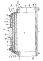
In the composite semiconductor device of Example 15 shown in FIGS. 20 to 22, the light emitting element, the protective element, and the light receiving element, that is, the photoelectric conversion element or the optical sensor are combined, and the light emitting element portion 1, the protective element portion 2, and the light receiving element are combined. And an element portion 90.

図20及び図21に示す保護素子部2は、その平面形状が図21に示すように変形された他は図1及び図2と同一に構成されている。即ち、図20から保護膜12を省いて複合半導体装置を示す図21から明らかように保護素子部2における保護素子用n型半導体薄膜11は、発光半導体領域7の側面17のほぼ半周即ち左半分と基板3の外周部分32のほぼ半周即ち左半分に配置されている。
なお、図20の保護素子部2の代りに図8の保護素子部2d、図10の保護素子部2f、図12の保護素子部2g、図13の保護素子部2h、図14の保護素子部2i、又は図15の保護素子部2j等を設けることができる。
20 and FIG. 21 has the same configuration as that of FIG. 1 and FIG. 2 except that its planar shape is modified as shown in FIG. That is, the protective element n-type semiconductor thin film 11 in the protective element portion 2 is substantially half the circumference of the side surface 17 of the light emitting semiconductor region 7, that is, the left half, as is clear from FIG. The outer peripheral portion 32 of the substrate 3 is arranged almost half the circumference, that is, the left half.
20 instead of the protective element unit 2 in FIG. 20, the protective element unit 2f in FIG. 10, the protective element unit 2f in FIG. 10, the protective element unit 2g in FIG. 12, the protective element unit 2h in FIG. 13, and the protective element unit in FIG. 2i, the protection element portion 2j in FIG. 15, and the like can be provided.

受光素子部90は受光素子としてのホトダイオードを構成するための部分であって、基板3の延長部分としての外周部分32の右半分と、受光素子用n型半導体薄膜91と、受光素子用電極層92とから成る。   The light receiving element portion 90 is a portion for constituting a photodiode as a light receiving element, and is a right half of an outer peripheral portion 32 as an extended portion of the substrate 3, a light receiving element n-type semiconductor thin film 91, and a light receiving element electrode layer. 92.

受光素子用n型半導体薄膜91は、保護素子用n型半導体薄膜11の下の絶縁膜10の延長部分に相当する光透過性を有する絶縁膜10´の上に配置されている部分とp型半導体基板3の外周部分32にpn接触している部分とを有する。この受光素子用n型半導体薄膜91は、保護素子用n型半導体薄膜11と同一材料且つ同一方法で形成することができる。受光素子用電極層92は、受光素子用n型半導体薄膜91の上に金属を被着させることによって形成されている。なお、p型半導体基板3及び受光素子用n型半導体薄膜91は発光半導体領域7から放射された光を吸収できる材料(例えばシリコン)で形成される。   The n-type semiconductor thin film 91 for the light receiving element includes a portion disposed on the insulating film 10 ′ having optical transparency corresponding to an extended portion of the insulating film 10 below the n-type semiconductor thin film 11 for the protective element, and a p-type. And a portion in pn contact with the outer peripheral portion 32 of the semiconductor substrate 3. The n-type semiconductor thin film 91 for the light receiving element can be formed by the same material and the same method as the n-type semiconductor thin film 11 for the protective element. The light receiving element electrode layer 92 is formed by depositing a metal on the light receiving element n-type semiconductor thin film 91. The p-type semiconductor substrate 3 and the n-type semiconductor thin film 91 for the light receiving element are formed of a material (for example, silicon) that can absorb the light emitted from the light emitting semiconductor region 7.

図20及び図21の実施例15の複合半導体装置は、図22の等価回路で示すことができる。図22における発光ダイオード41と保護ダイオード42とは、実施例1と同様に発光素子部1と保護素子部2とで形成されている。ホトダイオード93は、受光素子部90によって形成されている。ホトダイオード93のアノードは図20の第2の電極9に対応する第2の端子44に接続され、カソードは図20の受光素子用電極層92に対応する第3の端子94に接続されている。   The composite semiconductor device according to the fifteenth embodiment shown in FIGS. 20 and 21 can be represented by an equivalent circuit shown in FIG. The light emitting diode 41 and the protection diode 42 in FIG. 22 are formed of the light emitting element portion 1 and the protection element portion 2 as in the first embodiment. The photodiode 93 is formed by the light receiving element portion 90. The anode of the photodiode 93 is connected to the second terminal 44 corresponding to the second electrode 9 of FIG. 20, and the cathode is connected to the third terminal 94 corresponding to the light receiving element electrode layer 92 of FIG.

ホトダイオード93は、発光ダイオード41の発光状態の検出のために使用される。即ち、発光半導体領域7から放射された光の一部はp型半導体基板3の外周部分32と受光素子用n型半導体領域91とで形成されているpn接合に至り、ここで吸収されて電気パワーに変換される。更に詳細には、窒化物半導体から成る発光半導体領域7のバンドギャップはシリコン半導体基板3のバンドギャップよりも大きいので、シリコン半導体基板3のバンドギャップよりも大きなエネルギーを持った波長の光が発光半導体領域7から発生し、この光の一部がシリコン半導体基板3の外周部分32と受光素子用n型半導体薄膜91とから成るの受光素子部分90において電気エネルギーに変換される。図22においてホトダイオード93から出力を得るために第2の端子44及び第3の端子94に周知の出力回路(図示せず)が接続される。この出力回路は発光半導体領域7から放射された光量又は光束に所望の関数関係(例えば、比例関係)を有する出力電流又は電圧を出力する。   The photodiode 93 is used for detecting the light emission state of the light emitting diode 41. That is, a part of the light emitted from the light emitting semiconductor region 7 reaches the pn junction formed by the outer peripheral portion 32 of the p-type semiconductor substrate 3 and the n-type semiconductor region 91 for the light receiving element, and is absorbed and electric. Converted to power. More specifically, since the band gap of the light emitting semiconductor region 7 made of a nitride semiconductor is larger than the band gap of the silicon semiconductor substrate 3, light having a wavelength having energy larger than the band gap of the silicon semiconductor substrate 3 is emitted from the light emitting semiconductor. A part of the light generated from the region 7 is converted into electric energy in the light receiving element portion 90 formed of the outer peripheral portion 32 of the silicon semiconductor substrate 3 and the n-type semiconductor thin film 91 for the light receiving element. In FIG. 22, a known output circuit (not shown) is connected to the second terminal 44 and the third terminal 94 in order to obtain an output from the photodiode 93. This output circuit outputs an output current or voltage having a desired functional relationship (for example, a proportional relationship) to the light amount or light flux emitted from the light emitting semiconductor region 7.

この実施例15は、実施例1と同一の効果を有する他に、次の効果を有する。
(1) 受光素子としてのホトダイオード93が発光素子としての発光ダイオード41に一体化されているので、発光ダイオード41の発光状態を正確且つ容易にモニターすることができる。また発光ダイオード41の明るさをホトダイオード93でモニターし、発光ダイオード41の明るさを制御することが可能になる。
(2) ホトダイオード93はp型シリコン半導体基板3の外周部分32と発光半導体領域7の側面17に配置された受光素子用n型半導体薄膜91との組み合せで構成されているので、ホトダイオード93を小型且つ安価に形成することができる。なお、既に説明したようにp型シリコン半導体基板3の外周部分32は発光素子を形成する時に必然的に生じる部分であるので、受光素子を設けることによる半導体基板3のサイズの実質的な増大を招かない。
(3) ホトダイオード93は保護ダイオード42と同一の材料及び同一の方法で形成されているので、複合半導体装置の低コスト化を達成できる。
(4) 第2の電極9を発光素子と保護素子と受光素子とで共用しているので、小型化及び低コスト化を達成できる。
The fifteenth embodiment has the following effects in addition to the same effects as the first embodiment.
(1) Since the photodiode 93 as the light receiving element is integrated with the light emitting diode 41 as the light emitting element, the light emission state of the light emitting diode 41 can be monitored accurately and easily. Also, the brightness of the light emitting diode 41 can be controlled by monitoring the brightness of the light emitting diode 41 with the photodiode 93.
(2) Since the photodiode 93 is composed of a combination of the outer peripheral portion 32 of the p-type silicon semiconductor substrate 3 and the n-type semiconductor thin film 91 for the light receiving element disposed on the side surface 17 of the light emitting semiconductor region 7, the photodiode 93 is reduced in size. Moreover, it can be formed at low cost. As already described, the outer peripheral portion 32 of the p-type silicon semiconductor substrate 3 is a portion that inevitably occurs when the light emitting element is formed. Therefore, the substantial increase in the size of the semiconductor substrate 3 due to the provision of the light receiving element. Do not invite.
(3) Since the photodiode 93 is formed of the same material and the same method as the protection diode 42, the cost of the composite semiconductor device can be reduced.
(4) Since the second electrode 9 is shared by the light emitting element, the protective element, and the light receiving element, it is possible to achieve downsizing and cost reduction.

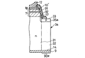
図23に実施例16の複合半導体装置の一部が示されている。この実施例16の複合半導体装置は、図20及び図21に示す実施例15の複合半導体装置の受光素子部90を受光素子部90aに変形し、且つ図20及び図21の保護素子部2の構成を図8の保護素子部2dに変形したものに相当する。   FIG. 23 shows a part of the composite semiconductor device of Example 16. In the composite semiconductor device of this sixteenth embodiment, the light receiving element portion 90 of the composite semiconductor device of the fifteenth embodiment shown in FIGS. 20 and 21 is transformed into a light receiving element portion 90a, and the protection element portion 2 of FIG. 20 and FIG. The configuration corresponds to a modification of the protection element portion 2d of FIG.

図23の受光素子部90aは、図20及び図21の実施例15の受光素子部90と同様にシリコン半導体基板3の外周部分32の右半分と発光半導体領域7の側面17の右半分とに形成され、受光素子用のp型半導体薄膜95とn型半導体薄膜91と電極層92とを有する。   The light receiving element portion 90a of FIG. 23 is formed on the right half of the outer peripheral portion 32 of the silicon semiconductor substrate 3 and the right half of the side surface 17 of the light emitting semiconductor region 7 in the same manner as the light receiving element portion 90 of the fifteenth embodiment of FIGS. A p-type semiconductor thin film 95, an n-type semiconductor thin film 91, and an electrode layer 92 for the light receiving element are formed.

受光素子用p型半導体薄膜95は図8の保護素子用p型半導体薄膜50と同一材料且つ同一方法で形成され、p型シリコン半導体基板3の外周部分32に電気的に接続されている部分と光透過性を有する絶縁膜10´を介して発光半導体領域7の側面17上に配置されている部分とを有する。   The p-type semiconductor thin film 95 for the light receiving element is formed of the same material and in the same method as the p-type semiconductor thin film 50 for the protective element in FIG. 8 and is electrically connected to the outer peripheral portion 32 of the p-type silicon semiconductor substrate 3. And a portion disposed on the side surface 17 of the light emitting semiconductor region 7 through the light-transmitting insulating film 10 ′.

図23の受光素子用n型半導体薄膜91は、図8の保護素子用n型半導体薄膜11と同一材料且つ同一方法で形成され、且つp型半導体薄膜95にpn接触している部分と光透過性を有する絶縁膜10´を介して側面17に対向配置されている部分とを有する。受光素子用p型半導体薄膜95及び受光素子用n型半導体薄膜91は、発光半導体領域7から放射された光を吸収できる材料(例えばシリコン)で形成される。従って、受光素子用p型半導体薄膜95及び受光素子用n型半導体薄膜91とで形成されるホトダイオードは図20の実施例15のホトダイオードと同様に機能する。   The n-type semiconductor thin film 91 for the light receiving element in FIG. 23 is formed of the same material and by the same method as the n-type semiconductor thin film 11 for the protective element in FIG. And a portion opposed to the side surface 17 through the insulating film 10 'having the property. The p-type semiconductor thin film 95 for the light receiving element and the n-type semiconductor thin film 91 for the light receiving element are formed of a material (for example, silicon) that can absorb the light emitted from the light emitting semiconductor region 7. Accordingly, the photodiode formed by the p-type semiconductor thin film 95 for the light receiving element and the n-type semiconductor thin film 91 for the light receiving element functions in the same manner as the photodiode of the embodiment 15 of FIG.

受光素子用電極層92は、図20と同様にn型半導体薄膜91に電気的に接続されている。受光素子部90aにおけるp型シリコン半導体基板3の外周部分32はp型半導体薄膜95を第2の電極9に電気的に接続する機能を有する。なお、この受光素子部90aにおける外周部分32は発光半導体領域7から放射された光を吸収できる材料から選択されたシリコン半導体から成るので、光導電効果を有し、発光半導体領域7から光が発生した時に導電率が増加する。   The light receiving element electrode layer 92 is electrically connected to the n-type semiconductor thin film 91 as in FIG. The outer peripheral portion 32 of the p-type silicon semiconductor substrate 3 in the light receiving element portion 90 a has a function of electrically connecting the p-type semiconductor thin film 95 to the second electrode 9. Since the outer peripheral portion 32 of the light receiving element portion 90a is made of a silicon semiconductor selected from a material capable of absorbing light emitted from the light emitting semiconductor region 7, it has a photoconductive effect and light is generated from the light emitting semiconductor region 7. Conductivity increases.

図23の実施例16の複合半導体装置は、図20の実施例15と同一の効果を有する。   The composite semiconductor device of Example 16 of FIG. 23 has the same effect as that of Example 15 of FIG.

図23の複合半導体装置の図示が省略されている保護素子部は、コストの低減のために図8と同様に形成されているが、この代りに図1の保護素子部2、図10の保護素子部2f、図12の保護素子部2g、図13の保護素子部2h、図14の保護素子部2i、又は図15の保護素子部2j等を設けることができる。   Although the protection element portion of the composite semiconductor device of FIG. 23 not shown is formed in the same manner as in FIG. 8 in order to reduce costs, the protection element portion 2 in FIG. 1 and the protection element in FIG. The element portion 2f, the protective element portion 2g in FIG. 12, the protective element portion 2h in FIG. 13, the protective element portion 2i in FIG. 14, or the protective element portion 2j in FIG. 15 can be provided.

図24に実施例17の複合半導体装置の一部が示されている。この実施例17の複合半導体装置は、図20及び図21に示す実施例15のp型シリコン半導体基板3をn型シリコン半導体基板3aに変形し、且つ受光素子部90をホトトランジスタ機能を有する受光素子部90bに変形し、且つ図20及び図21の保護素子部2の構成を図10の保護素子部2fに変形したものに相当する。   FIG. 24 shows a part of the composite semiconductor device according to the seventeenth embodiment. In the composite semiconductor device according to the seventeenth embodiment, the p-type silicon semiconductor substrate 3 according to the fifteenth embodiment shown in FIGS. 20 and 21 is transformed into an n-type silicon semiconductor substrate 3a, and the light receiving element portion 90 has a phototransistor function. The element portion 90b is modified, and the configuration of the protection element portion 2 shown in FIGS. 20 and 21 is equivalent to the protection element portion 2f shown in FIG.

図24の受光素子部90bは、図20及び図21の実施例15の受光素子部90と同様にシリコン半導体基板3の外周部分32の右半分と発光半導体領域7の側面17の右半分とに形成され、npn型受光素子用のn型半導体薄膜61aとp型半導体薄膜62aとn型半導体薄膜63aと電極層92とを有する。   The light receiving element portion 90b of FIG. 24 is formed on the right half of the outer peripheral portion 32 of the silicon semiconductor substrate 3 and the right half of the side surface 17 of the light emitting semiconductor region 7 in the same manner as the light receiving element portion 90 of the fifteenth embodiment of FIGS. An n-type semiconductor thin film 61a, a p-type semiconductor thin film 62a, an n-type semiconductor thin film 63a, and an electrode layer 92 for the npn light-receiving element are formed.

受光素子用n型半導体薄膜61aは図10の保護素子用n型半導体薄膜61と同一材料及び同一方法で形成され、且つn型半導体基板3aの外周部分32に電気的に接続された部分と光透過性を有する絶縁膜10´を介して発光半導体領域7の側面17に対向配置された部分とを有する。なお、受光素子用n型半導体薄膜61aとn型半導体基板3aの外周部分32との間に金属層を配置することができる。   The n-type semiconductor thin film 61a for the light receiving element is formed of the same material and by the same method as the n-type semiconductor thin film 61 for the protective element of FIG. 10, and is electrically connected to the outer peripheral portion 32 of the n-type semiconductor substrate 3a. And a portion disposed opposite to the side surface 17 of the light-emitting semiconductor region 7 with a transparent insulating film 10 'interposed therebetween. In addition, a metal layer can be arrange | positioned between the n-type semiconductor thin film 61a for light receiving elements, and the outer peripheral part 32 of the n-type semiconductor substrate 3a.

受光素子用p型半導体薄膜62aは図10の保護素子用p型半導体薄膜61と同一材料且つ同一方法で形成され、n型半導体薄膜61aにpn接触している部分と光透過性を有する絶縁膜10´を介して発光半導体領域7の側面17上に配置されている部分とを有する。   The p-type semiconductor thin film 62a for the light-receiving element is formed of the same material and by the same method as the p-type semiconductor thin film 61 for the protective element in FIG. 10, and an insulating film having a light transmission property with a portion pn contacting the n-type semiconductor thin film 61a. 10 'and the part arrange | positioned on the side surface 17 of the light emitting semiconductor region 7.

図24の受光素子用n型半導体薄膜63aは、図10の保護素子用n型半導体薄膜63と同一材料且つ同一方法で形成され、p型半導体薄膜62aにpn接触している部分と光透過性を有する絶縁膜10´を介して側面17に対向配置されている部分とを有する。なお、受光素子用n型半導体薄膜61a、受光素子用p型半導体薄膜62a及び受光素子用n型半導体薄膜63aは、発光半導体領域7から放射された光を吸収できる材料(例えばシリコン)で形成される。   The n-type semiconductor thin film 63a for the light receiving element in FIG. 24 is formed of the same material and in the same method as the n-type semiconductor thin film 63 for the protective element in FIG. 10, and is light transmissive with the portion in pn contact with the p-type semiconductor thin film 62a. And a portion opposed to the side surface 17 through an insulating film 10 ′ having The n-type semiconductor thin film 61a for the light receiving element, the p-type semiconductor thin film 62a for the light receiving element, and the n-type semiconductor thin film 63a for the light receiving element are formed of a material (for example, silicon) that can absorb the light emitted from the light emitting semiconductor region 7. The

受光素子用電極層92は、n型半導体薄膜63aに電気的に接続されている。受光素子部90bにおけるn型シリコン半導体基板3aの外周部分32はn型半導体薄膜61aを第2の電極9に電気的に接続する機能を有する。なお、この受光素子部90bにおける外周部分32はシリコン半導体から成るので、光導電効果を有し、発光半導体領域7から光が発生した時に導電率が増加する。   The light receiving element electrode layer 92 is electrically connected to the n-type semiconductor thin film 63a. The outer peripheral portion 32 of the n-type silicon semiconductor substrate 3a in the light receiving element portion 90b has a function of electrically connecting the n-type semiconductor thin film 61a to the second electrode 9. Since the outer peripheral portion 32 of the light receiving element portion 90b is made of a silicon semiconductor, it has a photoconductive effect, and the conductivity increases when light is generated from the light emitting semiconductor region 7.

図24の実施例17のn型半導体薄膜61aとp型半導体薄膜62aとn型半導体薄膜63aとから成るnpn3層構成はホトトランジスタとして機能する。ホトトランジスタはホトダイオードと同様に光パワーを電気パワーに変換する機能を有するので、図24の複合半導体装置は、図20の実施例15と同一の効果を有する。   The npn3 layer structure composed of the n-type semiconductor thin film 61a, the p-type semiconductor thin film 62a and the n-type semiconductor thin film 63a in Example 17 of FIG. 24 functions as a phototransistor. Since the phototransistor has a function of converting optical power into electric power like the photodiode, the composite semiconductor device of FIG. 24 has the same effect as that of the embodiment 15 of FIG.

図24の複合半導体装置の図示が省略されている保護素子部は、コストの低減のために図10と同様に形成されているが、この代りに図1の保護素子部2、図8の保護素子2d、図12の保護素子部2g、図13の保護素子部2h、図14の保護素子部2i、又は図15の保護素子部2j等を設けることができる。   The protective element portion of the composite semiconductor device in FIG. 24 that is not shown is formed in the same manner as in FIG. 10 in order to reduce the cost. Instead, the protective element portion 2 in FIG. 1 and the protective element portion in FIG. The element 2d, the protective element portion 2g in FIG. 12, the protective element portion 2h in FIG. 13, the protective element portion 2i in FIG. 14, or the protective element portion 2j in FIG. 15 can be provided.

図25に実施例18の複合半導体装置の一部が示されている。この実施例18の複合半導体装置は、図20及び図21に示す実施例15の複合半導体装置の受光素子部90をショットキーダイオードから成る受光素子部90cに変形し、且つ図20及び図21の保護素子部2の構成を図12の保護素子部2gに変形したものに相当する。   FIG. 25 shows a part of the composite semiconductor device of Example 18. In the composite semiconductor device of the eighteenth embodiment, the light receiving element portion 90 of the composite semiconductor device of the fifteenth embodiment shown in FIGS. 20 and 21 is transformed into a light receiving element portion 90c made of a Schottky diode, and the composite semiconductor device of FIGS. This corresponds to a modification of the protection element portion 2 to the protection element portion 2g of FIG.

図25の受光素子部90cは、図20及び図21の実施例15の受光素子部90と同様にシリコン半導体基板3の外周部分32の右半分と発光半導体領域7の側面17の右半分とに形成され、ショットキー電極として機能する金属層70aを有する。   The light receiving element portion 90c of FIG. 25 is formed on the right half of the outer peripheral portion 32 of the silicon semiconductor substrate 3 and the right half of the side surface 17 of the light emitting semiconductor region 7 in the same manner as the light receiving element portion 90 of the fifteenth embodiment of FIGS. A metal layer 70a is formed and functions as a Schottky electrode.

受光素子部90cにおける金属層70aは、図12の保護素子部2gにおける金属層70と同一材料且つ同一方法で形成され、p型シリコン半導体基板3の外周部分32にショットキー接触している部分と絶縁膜10´を介して発光半導体領域7の側面17上に配置されている部分とを有する。   The metal layer 70a in the light receiving element portion 90c is formed of the same material and in the same method as the metal layer 70 in the protective element portion 2g of FIG. 12, and is in a Schottky contact with the outer peripheral portion 32 of the p-type silicon semiconductor substrate 3. And a portion disposed on the side surface 17 of the light emitting semiconductor region 7 through the insulating film 10 ′.

受光素子部90cの金属層70aは、図22の第3の端子94と同様に受光出力端子として機能する。受光素子部90cにおけるp型シリコン半導体基板3の外周部分32は金属層70aを伴ってショットキーダイオードを構成する機能の他に、これを第2の電極9に電気的に接続する機能を有する。なお、この受光素子部90cにおける外周部分32はシリコン半導体から成るので、光導電効果を有し、発光半導体領域7から光が発生した時に導電率が増加する。なお、金属層70aがショットキー接触する半導体基板3を、シリコン以外の発光半導体領域7から放射された光を吸収できる材料で形成することができる。   The metal layer 70a of the light receiving element portion 90c functions as a light receiving output terminal similarly to the third terminal 94 in FIG. The outer peripheral portion 32 of the p-type silicon semiconductor substrate 3 in the light receiving element portion 90c has a function of electrically connecting it to the second electrode 9 in addition to the function of forming a Schottky diode with the metal layer 70a. Since the outer peripheral portion 32 in the light receiving element portion 90c is made of a silicon semiconductor, it has a photoconductive effect, and the conductivity increases when light is generated from the light emitting semiconductor region 7. The semiconductor substrate 3 with which the metal layer 70a is in Schottky contact can be formed of a material that can absorb light emitted from the light emitting semiconductor region 7 other than silicon.

図25の実施例18の複合半導体装置は、図20の実施例15と同一の効果を有する。   The composite semiconductor device of Example 18 of FIG. 25 has the same effect as that of Example 15 of FIG.

図25の複合半導体装置の図示が省略されている保護素子部は、コストの低減のために図12と同様に形成されているが、この代りに図1の保護素子部2、図8の保護素子部2d、図10の保護素子2f、図13の保護素子部2h、図14の保護素子部2i、又は図15の保護素子部2j等を設けることができる。   The protective element portion in which the illustration of the composite semiconductor device in FIG. 25 is omitted is formed in the same manner as in FIG. 12 in order to reduce costs, but instead of the protective element portion 2 in FIG. The element portion 2d, the protective element 2f in FIG. 10, the protective element portion 2h in FIG. 13, the protective element portion 2i in FIG. 14, or the protective element portion 2j in FIG. 15 can be provided.

図26に実施例19の複合半導体装置が示されている。この実施例19の複合半導体装置は、図20及び図21に示す実施例15の複合半導体装置の受光素子部90dをホトダイオードから成る受光素子部90aに変形し、且つ図20及び図21の保護素子部2の構成を図13の保護素子部2hに変形したものに相当する。   FIG. 26 shows a composite semiconductor device of Example 19. In the composite semiconductor device of the nineteenth embodiment, the light receiving element portion 90d of the composite semiconductor device of the fifteenth embodiment shown in FIGS. 20 and 21 is transformed into a light receiving element portion 90a made of a photodiode, and the protective element of FIGS. The configuration of the portion 2 corresponds to a modification of the protection element portion 2h of FIG.

図26の受光素子部90dは、図20及び図21の実施例15の受光素子部90と同様にシリコン半導体基板3の外周部分32の右半分と発光半導体領域7の側面17の右半分とに形成され、受光素子用のn型半導体領域34aと金属層71aとを有する。   The light receiving element portion 90d of FIG. 26 is formed on the right half of the outer peripheral portion 32 of the silicon semiconductor substrate 3 and the right half of the side surface 17 of the light emitting semiconductor region 7 in the same manner as the light receiving element portion 90 of the fifteenth embodiment of FIGS. An n-type semiconductor region 34a for the light receiving element and a metal layer 71a are formed.

受光素子用n型半導体領域34aは図13の保護素子用n型半導体領域34と同一材料且つ同一方法でp型半導体基板3内に形成されている。即ち、ホトダイオードを構成するための受光素子用n型半導体領域34aは、これとp型半導体基板3の外周部分32との間にpn接合を生じさせるために、p型シリコン半導体基板3の外周部分32の一方の主面33側に形成されている。半導体基板3及び受光素子用n型半導体領域34aを、シリコン以外の発光半導体領域7から放射された光を吸収できる材料で形成することができる。   The n-type semiconductor region 34a for the light receiving element is formed in the p-type semiconductor substrate 3 by the same material and the same method as the n-type semiconductor region 34 for the protective element in FIG. That is, the n-type semiconductor region 34a for the light receiving element for constituting the photodiode has a peripheral portion of the p-type silicon semiconductor substrate 3 in order to form a pn junction between the n-type semiconductor region 34a and the peripheral portion 32 of the p-type semiconductor substrate 3. 32 is formed on one main surface 33 side. The semiconductor substrate 3 and the n-type semiconductor region 34a for the light receiving element can be formed of a material that can absorb light emitted from the light emitting semiconductor region 7 other than silicon.

受光素子用金属層71aは、図13の保護素子用金属層71と同様に絶縁膜10´の上に形成され、その一端はn型半導体領域34aに電気的に接続されている。受光素子部90dにおけるp型シリコン半導体基板3の外周部分32はホトダイオードのp型領域として機能すると共に、このホトダイオードを第2の電極9に電気的に接続する機能を有する。なお、この受光素子部90dにおける外周部分32はシリコン半導体から成るので、光導電効果を有し、発光半導体領域7から光が発生した時に導電率が増加する。   The light receiving element metal layer 71a is formed on the insulating film 10 'similarly to the protective element metal layer 71 of FIG. 13, and one end thereof is electrically connected to the n-type semiconductor region 34a. The outer peripheral portion 32 of the p-type silicon semiconductor substrate 3 in the light receiving element portion 90d functions as a p-type region of the photodiode and has a function of electrically connecting the photodiode to the second electrode 9. Since the outer peripheral portion 32 of the light receiving element portion 90d is made of a silicon semiconductor, it has a photoconductive effect, and the conductivity increases when light is generated from the light emitting semiconductor region 7.

図26の実施例19の複合半導体装置は、図20の実施例15と同一の効果を有する。   The composite semiconductor device of Example 19 shown in FIG. 26 has the same effect as that of Example 15 of FIG.

図26の複合半導体装置の保護素子部2hの代りに図1の保護素子部2、図8の保護素子部2d、図10の保護素子2f、図12の保護素子部2g、図14の保護素子部2i、又は図15の保護素子部2j等を設けることもできる。   26, instead of the protective element 2h of the composite semiconductor device of FIG. 26, the protective element 2 of FIG. 8, the protective element 2d of FIG. 8, the protective element 2f of FIG. 10, the protective element 2g of FIG. 12, and the protective element of FIG. It is also possible to provide the portion 2i, the protection element portion 2j in FIG.

図27に実施例20の複合半導体装置の一部が示されている。この実施例20の複合半導体装置は、図20及び図21に示す実施例15の複合半導体装置のp型シリコン半導体基板3をn型シリコン半導体基板3aに変形し、且つ受光素子部90eをnpnホトトランジスタから成る受光素子部90eに変形し、且つ図20及び図21の保護素子部2の構成を図14の保護素子部2iに変形したものに相当する。   FIG. 27 shows a part of the composite semiconductor device of Example 20. In the composite semiconductor device of Example 20, the p-type silicon semiconductor substrate 3 of the composite semiconductor device of Example 15 shown in FIGS. 20 and 21 is transformed into an n-type silicon semiconductor substrate 3a, and the light receiving element portion 90e is changed to npn photo. This corresponds to a modification of the light receiving element portion 90e made of a transistor and a modification of the configuration of the protection element portion 2 in FIGS. 20 and 21 to the protection element portion 2i in FIG.

図27の受光素子部90eは、図20及び図21の実施例15の受光素子部90と同様にシリコン半導体基板3aの外周部分32の右半分と発光半導体領域7の側面17の右半分とに形成され、npnホトトランジスタを構成するための受光素子用のp型半導体領域35aと図20と同一のn型半導体薄膜91と電極層92とを有する。   The light receiving element portion 90e of FIG. 27 is formed on the right half of the outer peripheral portion 32 of the silicon semiconductor substrate 3a and the right half of the side surface 17 of the light emitting semiconductor region 7 in the same manner as the light receiving element portion 90 of the fifteenth embodiment of FIGS. A light-receiving element p-type semiconductor region 35a for forming an npn phototransistor, and an n-type semiconductor thin film 91 and an electrode layer 92 identical to those shown in FIG.

受光素子用p型半導体領域35aは図14の保護素子用p型半導体領域35と同一材料且つ同一方法で形成され、n型シリコン半導体基板3aの外周部分32の一方の主面33に露出している。   The p-type semiconductor region 35a for the light receiving element is formed of the same material and by the same method as the p-type semiconductor region 35 for the protective element of FIG. 14, and is exposed on one main surface 33 of the outer peripheral portion 32 of the n-type silicon semiconductor substrate 3a. Yes.

図27の受光素子用n型半導体薄膜91は、図14の保護素子用n型半導体薄膜11と同一材料且つ同一方法で形成され、且つ半導体基板3aのp型半導体領域35aにpn接触している部分と光透過性を有する絶縁膜10´を介して側面17に対向配置されている部分とを有する。なお、半導体基板3a、受光素子用p型半導体領域35a及び受光素子用n型半導体薄膜91は、発光半導体領域7から放射された光を吸収できる材料(例えばシリコン)で形成される。   The n-type semiconductor thin film 91 for the light receiving element in FIG. 27 is formed of the same material and by the same method as the n-type semiconductor thin film 11 for the protective element in FIG. 14, and is in pn contact with the p-type semiconductor region 35a of the semiconductor substrate 3a. A portion and a portion disposed to face the side surface 17 with an insulating film 10 ′ having light transmissivity interposed therebetween. The semiconductor substrate 3a, the light receiving element p-type semiconductor region 35a, and the light receiving element n-type semiconductor thin film 91 are formed of a material (for example, silicon) that can absorb light emitted from the light emitting semiconductor region 7.

受光素子用電極層92は、n型半導体薄膜91に電気的に接続され、図22の第3の端子94と同様に受光出力端子として機能する。受光素子部90eにおけるp型シリコン半導体基板3aの外周部分32はp型半導体領域35aの形成に利用されていると共に、npnホトトランジスタを第2の電極9に電気的に接続する機能を有する。なお、この受光素子部90eにおける外周部分32はシリコン半導体から成るので、光導電効果を有し、発光半導体領域7から光が発生した時に導電率が増加する。   The light receiving element electrode layer 92 is electrically connected to the n-type semiconductor thin film 91 and functions as a light receiving output terminal in the same manner as the third terminal 94 of FIG. The outer peripheral portion 32 of the p-type silicon semiconductor substrate 3a in the light receiving element portion 90e is used for forming the p-type semiconductor region 35a and has a function of electrically connecting the npn phototransistor to the second electrode 9. Since the outer peripheral portion 32 in the light receiving element portion 90e is made of a silicon semiconductor, it has a photoconductive effect, and the conductivity increases when light is generated from the light emitting semiconductor region 7.

図27の実施例20の複合半導体装置は、n型シリコン半導体基板3aとp型半導体領域35aとn型半導体薄膜91とから成るnpnホトトランジスタを有するので、図20の実施例15と同一の効果を得ることができる。   27 includes the npn phototransistor comprising the n-type silicon semiconductor substrate 3a, the p-type semiconductor region 35a, and the n-type semiconductor thin film 91, and therefore the same effect as that of the embodiment 15 of FIG. Can be obtained.

図27の複合半導体装置の図示が省略されている保護素子部は、コスト低減のために図14と同様に形成されているが、この代りに図1の保護素子部2、図8の保護素子部2d、図10の保護素子2f、図12の保護素子部2g、図13の保護素子部2h、又は図15の保護素子部2j等を設けることができる。   The protective element portion in which the illustration of the composite semiconductor device in FIG. 27 is omitted is formed in the same manner as in FIG. 14 for cost reduction. Instead, the protective element portion 2 in FIG. 1 and the protective element in FIG. The protection element 2f in FIG. 10, the protection element 2f in FIG. 12, the protection element 2g in FIG. 12, the protection element 2h in FIG. 13, the protection element 2j in FIG.

図28に実施例21の複合半導体装置の一部が示されている。この実施例21の複合半導体装置は、図20及び図21に示す実施例15の複合半導体装置のp型シリコン半導体基板3をn型シリコン半導体基板3aに変形し、且つ受光素子部90をホトトランジスタから成る受光素子部90fに変形し、且つ図20及び図21の保護素子部2の構成を図15の保護素子部2jに変形したものに相当する。   FIG. 28 shows a part of the composite semiconductor device of Example 21. In the composite semiconductor device of Example 21, the p-type silicon semiconductor substrate 3 of the composite semiconductor device of Example 15 shown in FIGS. 20 and 21 is transformed into an n-type silicon semiconductor substrate 3a, and the light receiving element portion 90 is replaced with a phototransistor. The light receiving element unit 90f is modified, and the configuration of the protection element unit 2 shown in FIGS. 20 and 21 corresponds to the protection element unit 2j shown in FIG.

図28の受光素子部90fは、図20及び図21の実施例15の受光素子部90と同様にシリコン半導体基板3aの外周部分32の右半分と発光半導体領域7の側面17の右半分とに形成され、受光素子用のp型半導体領域35aとn型半導体領域36aと金属層71aとを有する。   The light receiving element portion 90f of FIG. 28 is formed on the right half of the outer peripheral portion 32 of the silicon semiconductor substrate 3a and the right half of the side surface 17 of the light emitting semiconductor region 7 in the same manner as the light receiving element portion 90 of the fifteenth embodiment of FIGS. A p-type semiconductor region 35a, an n-type semiconductor region 36a for the light receiving element, and a metal layer 71a are formed.

受光素子用p型半導体領域35aは図15の保護素子用p型半導体領域35と同一材料且つ同一方法で形成され、p型シリコン半導体基板3aの外周部分32に配置されている。   The p-type semiconductor region 35a for the light receiving element is formed of the same material and by the same method as the p-type semiconductor region 35 for the protective element in FIG. 15, and is disposed on the outer peripheral portion 32 of the p-type silicon semiconductor substrate 3a.

図28の受光素子用n型半導体領域36aは、図15の保護素子用n型半導体領域36と同一材料且つ同一方法で形成され、且つp型半導体領域35aにpn接触している。半導体基板3a、受光素子用p型半導体領域35a及び受光素子用n型半導体領域36aを、シリコン以外の発光半導体領域7から放射された光を吸収できる材料で形成することができる。   The n-type semiconductor region 36a for the light receiving element in FIG. 28 is formed of the same material and in the same method as the n-type semiconductor region 36 for the protective element in FIG. 15, and is in pn contact with the p-type semiconductor region 35a. The semiconductor substrate 3a, the p-type semiconductor region 35a for the light receiving element, and the n-type semiconductor region 36a for the light receiving element can be formed of a material that can absorb light emitted from the light emitting semiconductor region 7 other than silicon.

受光素子用金属層71aは図15の保護素子用金属層71と同一材料且つ同一方法で形成され、n型半導体領域36aに電気的に接続され、図22の第3の端子94と同様な機能を有する。受光素子部90fにおけるn型シリコン半導体基板3aの外周部分32はnpnホトトランジスタの形成に使用されていると共に、このホトトランジスタを第2の電極9に電気的に接続するためにも使用されている。なお、この受光素子部90fにおける外周部分32はシリコン半導体から成るので、光導電効果を有し、発光半導体領域7から光が発生した時に導電率が増加する。   The light receiving element metal layer 71a is formed of the same material and in the same method as the protective element metal layer 71 of FIG. 15, is electrically connected to the n-type semiconductor region 36a, and has the same function as the third terminal 94 of FIG. Have The outer peripheral portion 32 of the n-type silicon semiconductor substrate 3a in the light receiving element portion 90f is used for forming an npn phototransistor and also used for electrically connecting the phototransistor to the second electrode 9. . In addition, since the outer peripheral portion 32 in the light receiving element portion 90f is made of a silicon semiconductor, it has a photoconductive effect, and the conductivity increases when light is generated from the light emitting semiconductor region 7.

図28の実施例21の複合半導体装置のnpnホトトランジスタは、ホトダイオードと同様に受光素子として機能するので、図28の実施例21は図20の実施例15と同一の効果を有する。   Since the npn phototransistor of the composite semiconductor device of Example 21 of FIG. 28 functions as a light receiving element in the same manner as the photodiode, Example 21 of FIG. 28 has the same effect as Example 15 of FIG.

図28の複合半導体装置の図示が省略されている保護素子部は、コスト低減のために図15と同様に形成されているが、この代りに図1の保護素子部2、図8の保護素子部2d、図10の保護素子2f、図12の保護素子部2g、図13の保護素子部2h、又は図14の保護素子部2i等を設けることができる。   The protective element portion of the composite semiconductor device of FIG. 28 not shown is formed in the same manner as FIG. 15 for cost reduction. Instead, the protective element portion 2 of FIG. 1 and the protective element of FIG. The protection element 2f in FIG. 10, the protection element 2f in FIG. 12, the protection element 2g in FIG. 12, the protection element 2h in FIG. 13, the protection element 2i in FIG.

本発明は上述の実施例に限定されるものでなく、例えば次の変形が可能なものである。
(1) 図5〜図10、図12〜図16、図18、図20、及び図23〜図28に示す実施例1〜13、及び15〜21の光透過性電極18、及び図19の帯状電極18aを省くこともできる。この場合には発光半導体領域7に周知の電流分散層を設けることが望ましい。
(2) 図8、図9、図10及び図16の半導体基板3,3aを金属基板に置き換えることができる。
(3) 発光半導体領域7から基板3,3a,3b側に放射された光を発光半導体領域7の第1の主面15側に反射させる機能を第2の電極9に与えること、又は独立した反射層を基板3,3a,3bの一方の主面13側又は他方の主面14側に設けることができる。
(4) 必要に応じて基板3,3aの他方の主面14から光を取り出すこともできる。
(5) 半導体基板3,3aの外周部分32の不純物濃度を中央部分31と異なる値にすることができる。
(6) 半導体基板3,3a、発光半導体領域7の各層4〜6、保護素子部2〜2mの各半導体薄膜11,50,61,62,63、基板内の半導体領域34,35,36、を実施例と反対の導電型にすることができる。
(7) シリコン半導体基板3又は3aを単結晶シリコン以外の多結晶シリコン又はSiC等のシリコン化合物、又は3−5族化合物半導体とすることができる。
(8) 半導体基板3又は3aの上に発光半導体領域7を気相成長させる代わりに、半導体基板3又は3a又は金属基板3bに発光半導体領域2を熱圧着等で貼り合わせることができる。
(9) 保護素子部2〜2lの保護素子に、これとは別の機能を有する保護素子、例えば、pn接合ダイオード、npn又はpnpの3層ダイオード、ショットキーダイオード、バリスタ、及びコンデンサ等から選択されたものを付加することができる。特にpn接合ダイオード等にコンデンサを並列に接続することは過電圧保護に有効である。
(10) 図1、図5〜図10、図13、図14、図16、図18及び図19の保護素子部における保護素子を、半導体薄膜で形成する代りに半導体厚膜で形成すること、又はダイオード、バリスタ、及びコンデンサ等の個別部品で形成すること、又は半導体薄膜と半導体厚膜と個別部品から選択された複数の組合せで形成することができる。
(11)受光素子としてホトダイオード又はホトトランジスタを設ける代わりに、光導電型受光素子(光導電型センサ)を設けることができる。光導電型受光素子は図25の金属層70aを光吸収可能な半導体基板3にオーミック接触させることによって得られる。なお、図25の半導体基板3は光導電効果を有するので、図25の受光素子をショットキーバリヤ型の受光素子と光導電型受光素子との組み合わせ素子と呼ぶこともできる。
(12)図20、図23〜図28の絶縁膜10の部分に、これに代わって保護膜12の延長部分を設けることができる。
(13)図20、図23〜図28の受光素子部に、光入力が要求されている箇所以外を覆うための遮光層を設けることができる。
The present invention is not limited to the above-described embodiments, and for example, the following modifications are possible.
(1) The light transmissive electrodes 18 of Examples 1 to 13 and 15 to 21 shown in FIGS. 5 to 10, 12 to 16, 18, 20, and 23 to 28, and FIG. 19. The strip electrode 18a can be omitted. In this case, it is desirable to provide a known current spreading layer in the light emitting semiconductor region 7.
(2) The semiconductor substrates 3 and 3a in FIGS. 8, 9, 10 and 16 can be replaced with metal substrates.
(3) Giving the second electrode 9 the function of reflecting the light emitted from the light emitting semiconductor region 7 toward the substrates 3, 3a, 3b to the first main surface 15 side of the light emitting semiconductor region 7, or independent The reflective layer can be provided on one main surface 13 side or the other main surface 14 side of the substrates 3, 3a, 3b.
(4) If necessary, light can be extracted from the other main surface 14 of the substrates 3 and 3a.
(5) The impurity concentration of the outer peripheral portion 32 of the semiconductor substrates 3 and 3a can be set to a value different from that of the central portion 31.
(6) Semiconductor substrates 3 and 3a, layers 4 to 6 of the light emitting semiconductor region 7, semiconductor thin films 11, 50, 61, 62, and 63 of the protection element portions 2 to 2m, semiconductor regions 34, 35, and 36 in the substrate, Can be made to have a conductivity type opposite to that of the embodiment.
(7) The silicon semiconductor substrate 3 or 3a may be polycrystalline silicon other than single crystal silicon, a silicon compound such as SiC, or a group 3-5 compound semiconductor.
(8) Instead of vapor growth of the light emitting semiconductor region 7 on the semiconductor substrate 3 or 3a, the light emitting semiconductor region 2 can be bonded to the semiconductor substrate 3 or 3a or the metal substrate 3b by thermocompression bonding or the like.
(9) Select a protective element having a function different from that of the protective element in the protective element units 2 to 21 from, for example, a pn junction diode, an npn or pnp three-layer diode, a Schottky diode, a varistor, and a capacitor. Can be added. In particular, connecting a capacitor in parallel to a pn junction diode or the like is effective for overvoltage protection.
(10) forming the protective element in the protective element part of FIGS. 1, 5 to 10, 13, 14, 16, 16, 18 and 19 with a semiconductor thick film instead of a semiconductor thin film; Alternatively, it can be formed by individual parts such as a diode, a varistor, and a capacitor, or can be formed by a plurality of combinations selected from a semiconductor thin film, a semiconductor thick film, and individual parts.
(11) Instead of providing a photodiode or a phototransistor as the light receiving element, a photoconductive light receiving element (photoconductive sensor) can be provided. The photoconductive light-receiving element is obtained by bringing the metal layer 70a of FIG. 25 into ohmic contact with the semiconductor substrate 3 capable of absorbing light. Since the semiconductor substrate 3 in FIG. 25 has a photoconductive effect, the light receiving element in FIG. 25 can also be called a combination element of a Schottky barrier type light receiving element and a photoconductive type light receiving element.
(12) An extended portion of the protective film 12 can be provided in place of the insulating film 10 in FIGS. 20 and 23 to 28.
(13) A light-shielding layer can be provided in the light-receiving element portion of FIGS. 20 and 23 to 28 to cover areas other than those where light input is required.

本発明は、半導体発光素子と保護素子との複合半導体装置に利用可能である。   The present invention is applicable to a composite semiconductor device including a semiconductor light emitting element and a protection element.

本発明の実施例1に従う複合半導体装置を概略的に示す中央縦断面図である。1 is a central longitudinal sectional view schematically showing a composite semiconductor device according to Embodiment 1 of the present invention. 図1の複合半導体装置の発光半導体領域及び半導体基板を縮小して示す平面図である。FIG. 2 is a plan view showing a light emitting semiconductor region and a semiconductor substrate of the composite semiconductor device of FIG. 1 in a reduced scale. 図1の発光半導体領域と半導体基板の一部を切断前のウエハ状態で示す断面図である。It is sectional drawing which shows the light emitting semiconductor region of FIG. 1, and a part of semiconductor substrate in the wafer state before a cutting | disconnection. 図1の複合半導体装置の電気回路図である。FIG. 2 is an electric circuit diagram of the composite semiconductor device of FIG. 1. 実施例2の複合半導体装置を概略的に示す中央縦断面図である。It is a center longitudinal cross-sectional view which shows the composite semiconductor device of Example 2 roughly. 実施例3の複合半導体装置を概略的に示す中央縦断面図である。FIG. 6 is a central longitudinal sectional view schematically showing a composite semiconductor device of Example 3. 実施例4の複合半導体装置を概略的に示す中央縦断面図である。FIG. 6 is a central longitudinal sectional view schematically showing a composite semiconductor device of Example 4. 実施例5の複合半導体装置を概略的に示す中央縦断面図である。FIG. 10 is a central longitudinal sectional view schematically showing a composite semiconductor device of Example 5. 実施例6の複合半導体装置を概略的に示す中央縦断面図である。FIG. 10 is a central longitudinal sectional view schematically showing a composite semiconductor device of Example 6. 実施例7の複合半導体装置を概略的に示す中央縦断面図である。FIG. 10 is a central longitudinal sectional view schematically showing a composite semiconductor device of Example 7. 図10の複合半導体装置の電気回路図である。FIG. 11 is an electric circuit diagram of the composite semiconductor device of FIG. 10. 実施例8の複合半導体装置を概略的に示す中央縦断面図である。FIG. 10 is a central longitudinal sectional view schematically showing a composite semiconductor device of Example 8. 実施例9の複合半導体装置を概略的に示す中央縦断面図である。FIG. 10 is a central longitudinal sectional view schematically showing a composite semiconductor device of Example 9. 実施例10の複合半導体装置を概略的に示す中央縦断面図である。It is a center longitudinal cross-sectional view which shows the composite semiconductor device of Example 10 roughly. 実施例11の複合半導体装置を概略的に示す中央縦断面図である。FIG. 10 is a central longitudinal sectional view schematically showing a composite semiconductor device of Example 11. 実施例12の複合半導体装置を概略的に示す中央縦断面図である。It is a center longitudinal cross-sectional view which shows the composite semiconductor device of Example 12 roughly. 図16の複合半導体装置の電気回路図である。FIG. 17 is an electric circuit diagram of the composite semiconductor device of FIG. 16. 実施例13の複合半導体装置を概略的に示す中央縦断面図である。It is a center longitudinal cross-sectional view which shows the composite semiconductor device of Example 13 roughly. 実施例14の複合半導体装置を概略的に示す中央縦断面図である。It is a center longitudinal cross-sectional view which shows the composite semiconductor device of Example 14 roughly. 実施例15の複合半導体装置を概略的に示す中央縦断面図である。FIG. 16 is a central longitudinal sectional view schematically showing a composite semiconductor device of Example 15. 図20の複合半導体装置を保護膜を省いて示す平面図である。FIG. 21 is a plan view showing the composite semiconductor device of FIG. 20 without a protective film. 図20の複合半導体装置の電気回路図である。FIG. 21 is an electric circuit diagram of the composite semiconductor device of FIG. 20. 実施例16の複合半導体装置の一部を概略的に示す中央縦断面図である。FIG. 16 is a central longitudinal sectional view schematically showing a part of a composite semiconductor device of Example 16. 実施例17の複合半導体装置の一部を概略的に示す中央縦断面図である。FIG. 16 is a central longitudinal sectional view schematically showing a part of a composite semiconductor device of Example 17. 実施例18の複合半導体装置の一部を概略的に示す中央縦断面図である。FIG. 26 is a central longitudinal sectional view schematically showing a part of a composite semiconductor device of Example 18; 実施例19の複合半導体装置を概略的に示す中央縦断面図である。42 is a central longitudinal sectional view schematically showing a composite semiconductor device of Example 19. FIG. 実施例20の複合半導体装置の一部を概略的に示す中央縦断面図である。FIG. 26 is a central longitudinal sectional view schematically showing a part of a composite semiconductor device of Example 20; 実施例21の複合半導体装置の一部を概略的に示す中央縦断面図である。22 is a central longitudinal sectional view schematically showing a part of a composite semiconductor device of Example 21. FIG. 従来の保護素子を伴う発光素子を示す電気回路図である。It is an electric circuit diagram which shows the light emitting element with the conventional protective element.

符号の説明Explanation of symbols

1〜1d 発光素子部
2〜2l 保護素子部
3,3a 半導体基板
7 発光半導体領域
8 第1の電極
9 第2の電極
10 絶縁膜
11 n型半導体薄膜
12 保護膜
DESCRIPTION OF SYMBOLS 1-1d Light emitting element part 2-21 Protection element part 3, 3a Semiconductor substrate 7 Light emitting semiconductor area | region 8 1st electrode 9 2nd electrode 10 Insulating film 11 n-type semiconductor thin film 12 Protective film

Claims (3)

半導体発光素子部とこの半導体発光素子部を過電圧から保護するための保護素子部とを含む複合半導体装置であって、
前記半導体発光素子部は、一方の主面と他方の主面とを有し且つ導電性を有し且つ第1導電型を有する半導体基板と、互いに対向する第1及び第2の主面と前記第1の主面から前記第2の主面に至る傾斜側面とを有し且つ前記第2の主面が前記半導体基板の一方の主面に電気的及び機械的に結合されている発光半導体領域と、前記発光半導体領域の前記第1の主面に配置された第1の電極と、前記半導体基板に接続された第2の電極とを備え、
前記保護素子部は、前記半導体基板の延長部分と前記発光半導体領域の前記傾斜側面に光透過性を有する絶縁膜を介して配置された光透過性を有する第2導電型半導体膜とから成り
前記第2導電型半導体膜の一端部分は前記半導体基板の前記延長部分にpn接合接触し、前記第2導電型半導体膜の他端部分は前記第1の電極に接続され、
前記第1の電極は光透過性を有し、
前記発光半導体領域は前記半導体基板の一方の主面上に気相成長された半導体又は前記半導体基板に熱圧着で貼り合わせた半導体からなることを特徴とする複合半導体装置。
A composite semiconductor device comprising a semiconductor light emitting element part and a protective element part for protecting the semiconductor light emitting element part from overvoltage,
The semiconductor light-emitting element section includes a semiconductor substrate having one main surface and the other main surface, having conductivity and having a first conductivity type, first and second main surfaces facing each other, and A light emitting semiconductor region having an inclined side surface extending from the first main surface to the second main surface, wherein the second main surface is electrically and mechanically coupled to one main surface of the semiconductor substrate. A first electrode disposed on the first main surface of the light emitting semiconductor region, and a second electrode connected to the semiconductor substrate,
The protection element portion includes an extended portion of the semiconductor substrate and a light-transmissive second conductive semiconductor film disposed on the inclined side surface of the light-emitting semiconductor region via a light-transmissive insulating film ,
One end portion of the second conductivity type semiconductor film is in pn junction contact with the extension portion of the semiconductor substrate, and the other end portion of the second conductivity type semiconductor film is connected to the first electrode,
The first electrode has optical transparency;
The light emitting semiconductor region is composed of a semiconductor grown in a vapor phase on one main surface of the semiconductor substrate or a semiconductor bonded to the semiconductor substrate by thermocompression bonding .
記第2導電型半導体膜は前記第1の電極の上を覆う部分を有し、前記覆部分は前記第1の電極を保護する機能を有していることを特徴とする請求項1記載の複合半導体装置。 Claims before Symbol second conductivity type semiconductor layer has a Cormorant part partial covering over of the first electrode, the covering cormorants portion, characterized in that has a function of protecting the first electrode Item 12. A composite semiconductor device according to Item 1. 前記第1の電極は、パッド電極機能を有している部分を備えていることを特徴とする請求項1又は2記載の複合半導体装置。 The first electrode, the composite semiconductor device according to claim 1, wherein that it comprises a part component that has a pad electrode function.
JP2005039649A 2005-02-16 2005-02-16 Composite semiconductor device Expired - Fee Related JP4697397B2 (en)

Priority Applications (4)

Application Number Priority Date Filing Date Title
JP2005039649A JP4697397B2 (en) 2005-02-16 2005-02-16 Composite semiconductor device
KR1020060000408A KR100765021B1 (en) 2005-02-16 2006-01-03 Composite semiconductor device
TW095100183A TWI289367B (en) 2005-02-16 2006-01-03 Compound semiconductor device
US11/343,798 US7449727B2 (en) 2005-02-16 2006-01-31 Overvoltage-protected light-emitting semiconductor device

Applications Claiming Priority (1)

Application Number Priority Date Filing Date Title
JP2005039649A JP4697397B2 (en) 2005-02-16 2005-02-16 Composite semiconductor device

Publications (2)

Publication Number Publication Date
JP2006228904A JP2006228904A (en) 2006-08-31
JP4697397B2 true JP4697397B2 (en) 2011-06-08

Family

ID=36815359

Family Applications (1)

Application Number Title Priority Date Filing Date
JP2005039649A Expired - Fee Related JP4697397B2 (en) 2005-02-16 2005-02-16 Composite semiconductor device

Country Status (4)

Country Link
US (1) US7449727B2 (en)
JP (1) JP4697397B2 (en)
KR (1) KR100765021B1 (en)
TW (1) TWI289367B (en)

Families Citing this family (50)

* Cited by examiner, † Cited by third party
Publication number Priority date Publication date Assignee Title
US7629751B2 (en) * 2006-03-03 2009-12-08 Chen-Jean Chou Electrical compensation and fault tolerant structure for light emitting device array
WO2007111432A1 (en) * 2006-03-28 2007-10-04 Seoul Opto Device Co., Ltd. Light emitting device having zener diode therein and method of fabricating the same
JP4221012B2 (en) * 2006-06-12 2009-02-12 トヨタ自動車株式会社 Semiconductor device and manufacturing method thereof
JP4929860B2 (en) * 2006-06-12 2012-05-09 株式会社デンソー Semiconductor device
US7714348B2 (en) * 2006-10-06 2010-05-11 Ac-Led Lighting, L.L.C. AC/DC light emitting diodes with integrated protection mechanism
JP5261923B2 (en) * 2006-10-17 2013-08-14 サンケン電気株式会社 Compound semiconductor device
JP4765916B2 (en) * 2006-12-04 2011-09-07 サンケン電気株式会社 Semiconductor light emitting device
DE102007013986A1 (en) * 2007-03-23 2008-09-25 Osram Opto Semiconductors Gmbh Optoelectronic component e.g. LED, has protective structure comprising material e.g. ceramic material or metal oxide e.g. zinc oxide, attached to structural element and/or to contact terminal, where material is provided as pasty mass
KR100856247B1 (en) * 2007-04-24 2008-09-03 삼성전기주식회사 Semiconductor light emitting device
DE102007043681B4 (en) * 2007-09-13 2022-01-20 OSRAM Opto Semiconductors Gesellschaft mit beschränkter Haftung optoelectronic component
DE102007061479A1 (en) * 2007-12-20 2009-06-25 Osram Opto Semiconductors Gmbh LED chip with surge protection
KR101438811B1 (en) * 2008-01-03 2014-09-05 엘지이노텍 주식회사 Semiconductor light emitting device and manufacturing method thereof
US8884321B2 (en) 2008-04-06 2014-11-11 Lg Innotek Co., Ltd. Luminous element
DE102008022942A1 (en) * 2008-05-09 2009-11-12 Osram Opto Semiconductors Gmbh Radiation-emitting semiconductor chip
JP2010003810A (en) * 2008-06-19 2010-01-07 Ae Tekku Kk Light-emitting diode-driving circuit
JP2010080950A (en) * 2008-08-29 2010-04-08 Semiconductor Energy Lab Co Ltd Solid-state dye laser
US8494021B2 (en) * 2008-08-29 2013-07-23 Semiconductor Energy Laboratory Co., Ltd. Organic laser device
KR101592201B1 (en) * 2008-11-06 2016-02-05 삼성전자 주식회사 Light emitting device and fabricating method thereof
JP4702442B2 (en) 2008-12-12 2011-06-15 ソニー株式会社 Semiconductor light emitting device and manufacturing method thereof
WO2010109572A1 (en) 2009-03-23 2010-09-30 トヨタ自動車株式会社 Semiconductor device
US9142592B2 (en) 2009-04-09 2015-09-22 Infineon Technologies Ag Integrated circuit including ESD device
JP5390918B2 (en) * 2009-04-14 2014-01-15 シャープ株式会社 Nonvolatile semiconductor memory device and manufacturing method thereof
WO2011093405A1 (en) * 2010-02-01 2011-08-04 有限会社Mtec Chip-size packaged optical semiconductor device
KR100974787B1 (en) * 2010-02-04 2010-08-06 엘지이노텍 주식회사 Light emitting device, method for fabricating the light emitting device and light emitting device package
DE102010034665B4 (en) 2010-08-18 2024-10-10 OSRAM Opto Semiconductors Gesellschaft mit beschränkter Haftung Optoelectronic semiconductor chip and method for producing optoelectronic semiconductor chips
US9159549B2 (en) 2011-05-26 2015-10-13 Shindengen Electric Manufacturing Co., Ltd. Glass composition for protecting semiconductor junction, method of manufacturing semiconductor device and semiconductor device
US9490239B2 (en) 2011-08-31 2016-11-08 Micron Technology, Inc. Solid state transducers with state detection, and associated systems and methods
US8809897B2 (en) 2011-08-31 2014-08-19 Micron Technology, Inc. Solid state transducer devices, including devices having integrated electrostatic discharge protection, and associated systems and methods
JP5543514B2 (en) 2012-03-23 2014-07-09 株式会社東芝 Semiconductor light emitting device and manufacturing method thereof
CN103890919B (en) * 2012-05-08 2016-07-06 新电元工业株式会社 Glass compound for semiconductor junction protection, manufacturing method of semiconductor device, and semiconductor device
JP5832956B2 (en) 2012-05-25 2015-12-16 株式会社東芝 Semiconductor light emitting device
CN104769691A (en) * 2012-11-02 2015-07-08 罗姆股份有限公司 Chip capacitors, circuit components, and electronic equipment
KR101967837B1 (en) 2013-03-11 2019-04-10 삼성전자주식회사 Semiconductor light-emitting device
DE102013103601A1 (en) * 2013-04-10 2014-10-16 Osram Opto Semiconductors Gmbh Optoelectronic component and method for producing an optoelectronic component
CN106575670B (en) 2014-09-18 2020-10-16 英特尔公司 Wurtzite heteroepitaxial structures with sloped sidewall facets for defect propagation control in silicon CMOS compatible semiconductor devices
WO2016048328A1 (en) 2014-09-25 2016-03-31 Intel Corporation Iii-n epitaxial device structures on free standing silicon mesas
US20160141335A1 (en) * 2014-11-18 2016-05-19 Intermolecular, Inc. Diamond Like Carbon (DLC) in a Semiconductor Stack as a Selector for Non-Volatile Memory Application
CN107078098B (en) 2014-11-18 2021-04-06 英特尔公司 CMOS circuit using N-channel and P-channel gallium nitride transistors
KR102423219B1 (en) 2014-12-18 2022-07-20 인텔 코포레이션 N-channel gallium nitride transistors
CN107949914B (en) 2015-05-19 2022-01-18 英特尔公司 Semiconductor device with raised doped crystal structure
WO2016209283A1 (en) 2015-06-26 2016-12-29 Intel Corporation Heteroepitaxial structures with high temperature stable substrate interface material
WO2017111869A1 (en) 2015-12-24 2017-06-29 Intel Corporation Transition metal dichalcogenides (tmdcs) over iii-nitride heteroepitaxial layers
KR101995161B1 (en) * 2017-02-23 2019-07-02 한국산업기술대학교산학협력단 Micro-light emitting diode light sources for sighting device and method for manufacturing the same
JP6809334B2 (en) * 2017-03-29 2021-01-06 Tdk株式会社 Semiconductor devices and their manufacturing methods
WO2019066953A1 (en) 2017-09-29 2019-04-04 Intel Corporation Group iii-nitride (iii-n) devices with reduced contact resistance and their methods of fabrication
US12125888B2 (en) 2017-09-29 2024-10-22 Intel Corporation Group III-nitride (III-N) devices with reduced contact resistance and their methods of fabrication
TWI666170B (en) * 2018-03-28 2019-07-21 鄭光煒 Heavy metal recycling device and use thereof
FR3093598B1 (en) * 2019-03-05 2023-08-04 St Microelectronics Srl Surge protection device
CN114078897A (en) * 2020-08-19 2022-02-22 京东方科技集团股份有限公司 Light-emitting device, preparation method thereof, display panel, backlight module and display device
FR3122769A1 (en) * 2021-05-07 2022-11-11 Stmicroelectronics (Tours) Sas One-way transient voltage suppression device without live conduction

Family Cites Families (9)

* Cited by examiner, † Cited by third party
Publication number Priority date Publication date Assignee Title
JP2592235B2 (en) * 1985-09-24 1997-03-19 ローム 株式会社 Semiconductor laser device
DE19612388C2 (en) * 1996-03-28 1999-11-04 Siemens Ag Integrated semiconductor circuit, in particular an optoelectronic component with overvoltage protection
JPH1065215A (en) * 1996-08-22 1998-03-06 Toyoda Gosei Co Ltd III-nitride semiconductor light emitting device
JP3787202B2 (en) * 1997-01-10 2006-06-21 ローム株式会社 Semiconductor light emitting device
US6333522B1 (en) * 1997-01-31 2001-12-25 Matsushita Electric Industrial Co., Ltd. Light-emitting element, semiconductor light-emitting device, and manufacturing methods therefor
JPH11298041A (en) * 1998-04-15 1999-10-29 Toyoda Gosei Co Ltd Group III nitride semiconductor light emitting device and light source device
TW492202B (en) * 2001-06-05 2002-06-21 South Epitaxy Corp Structure of III-V light emitting diode (LED) arranged in flip chip configuration having structure for preventing electrostatic discharge
TWI240969B (en) * 2003-06-06 2005-10-01 Sanken Electric Co Ltd Nitride semiconductor device and method for manufacturing same
CN100524790C (en) * 2004-02-02 2009-08-05 三垦电气株式会社 Light-emitting semiconductor element and composite semiconductor device of protection element

Also Published As

Publication number Publication date
JP2006228904A (en) 2006-08-31
KR100765021B1 (en) 2007-10-09
KR20060091718A (en) 2006-08-21
TW200631204A (en) 2006-09-01
TWI289367B (en) 2007-11-01
US7449727B2 (en) 2008-11-11
US20060181828A1 (en) 2006-08-17

Similar Documents

Publication Publication Date Title
JP4697397B2 (en) Composite semiconductor device
JP5044986B2 (en) Semiconductor light emitting device
US7173311B2 (en) Light-emitting semiconductor device with a built-in overvoltage protector
CN100423307C (en) Semiconductor light emitting device provided with protection diode element
JP5336030B2 (en) Light emitting device having a circuit protection unit
US7151281B2 (en) Light-emitting diode structure with electrostatic discharge protection
US6514782B1 (en) Method of making a III-nitride light-emitting device with increased light generating capability
KR101756333B1 (en) A light emitting device and a light emitting device package
JP4577497B2 (en) Composite semiconductor device of semiconductor light emitting element and protective element
US7105860B2 (en) Flip chip light-emitting diode package
JP5503572B2 (en) Light emitting element
US20070102692A1 (en) Semiconductor light emitting device
KR101116111B1 (en) Semiconductor light?emitting device
TWI557941B (en) Photoelectric element and method of manufacturing same
JP2007157926A (en) Semiconductor light emitting device with protective diode and its manufacturing method
KR20150002369A (en) Light emitting device package
KR102501191B1 (en) light emitting device
CN105140369B (en) Light emitting diode structure
KR20110119930A (en) Light emitting device, manufacturing method thereof and light emitting device package
KR102338140B1 (en) Semiconductor device
KR20250169559A (en) Light-emitting device
JP2007042682A (en) Composite semiconductor device of semiconductor light emitting element and protection element, and its manufacturing method
KR101633813B1 (en) A light emitting device and a method for fabricating the light emitting device and a light emitting device
KR101096751B1 (en) Semiconductor light emitting device

Legal Events

Date Code Title Description
A621 Written request for application examination

Free format text: JAPANESE INTERMEDIATE CODE: A621

Effective date: 20080111

A977 Report on retrieval

Free format text: JAPANESE INTERMEDIATE CODE: A971007

Effective date: 20100629

A131 Notification of reasons for refusal

Free format text: JAPANESE INTERMEDIATE CODE: A131

Effective date: 20100714

A521 Request for written amendment filed

Free format text: JAPANESE INTERMEDIATE CODE: A523

Effective date: 20100910

TRDD Decision of grant or rejection written
A01 Written decision to grant a patent or to grant a registration (utility model)

Free format text: JAPANESE INTERMEDIATE CODE: A01

Effective date: 20110202

A61 First payment of annual fees (during grant procedure)

Free format text: JAPANESE INTERMEDIATE CODE: A61

Effective date: 20110215

R150 Certificate of patent or registration of utility model

Ref document number: 4697397

Country of ref document: JP

Free format text: JAPANESE INTERMEDIATE CODE: R150

R250 Receipt of annual fees

Free format text: JAPANESE INTERMEDIATE CODE: R250

R250 Receipt of annual fees

Free format text: JAPANESE INTERMEDIATE CODE: R250

R250 Receipt of annual fees

Free format text: JAPANESE INTERMEDIATE CODE: R250

R250 Receipt of annual fees

Free format text: JAPANESE INTERMEDIATE CODE: R250

R250 Receipt of annual fees

Free format text: JAPANESE INTERMEDIATE CODE: R250

LAPS Cancellation because of no payment of annual fees