JP5336030B2 - Light emitting device having a circuit protection unit - Google Patents
Light emitting device having a circuit protection unit Download PDFInfo
- Publication number
- JP5336030B2 JP5336030B2 JP2005291277A JP2005291277A JP5336030B2 JP 5336030 B2 JP5336030 B2 JP 5336030B2 JP 2005291277 A JP2005291277 A JP 2005291277A JP 2005291277 A JP2005291277 A JP 2005291277A JP 5336030 B2 JP5336030 B2 JP 5336030B2
- Authority
- JP
- Japan
- Prior art keywords
- layer
- light emitting
- emitting device
- potential barrier
- barrier layer
- Prior art date
- Legal status (The legal status is an assumption and is not a legal conclusion. Google has not performed a legal analysis and makes no representation as to the accuracy of the status listed.)
- Expired - Fee Related
Links
Images


Classifications
-
- H—ELECTRICITY
- H01—ELECTRIC ELEMENTS
- H01L—SEMICONDUCTOR DEVICES NOT COVERED BY CLASS H10
- H01L33/00—Semiconductor devices with at least one potential-jump barrier or surface barrier specially adapted for light emission; Processes or apparatus specially adapted for the manufacture or treatment thereof or of parts thereof; Details thereof
- H01L33/36—Semiconductor devices with at least one potential-jump barrier or surface barrier specially adapted for light emission; Processes or apparatus specially adapted for the manufacture or treatment thereof or of parts thereof; Details thereof characterised by the electrodes
- H01L33/40—Materials therefor
-
- H—ELECTRICITY
- H01—ELECTRIC ELEMENTS
- H01L—SEMICONDUCTOR DEVICES NOT COVERED BY CLASS H10
- H01L27/00—Devices consisting of a plurality of semiconductor or other solid-state components formed in or on a common substrate
- H01L27/15—Devices consisting of a plurality of semiconductor or other solid-state components formed in or on a common substrate including semiconductor components with at least one potential-jump barrier or surface barrier specially adapted for light emission
-
- H—ELECTRICITY
- H01—ELECTRIC ELEMENTS
- H01L—SEMICONDUCTOR DEVICES NOT COVERED BY CLASS H10
- H01L2224/00—Indexing scheme for arrangements for connecting or disconnecting semiconductor or solid-state bodies and methods related thereto as covered by H01L24/00
- H01L2224/01—Means for bonding being attached to, or being formed on, the surface to be connected, e.g. chip-to-package, die-attach, "first-level" interconnects; Manufacturing methods related thereto
- H01L2224/10—Bump connectors; Manufacturing methods related thereto
- H01L2224/15—Structure, shape, material or disposition of the bump connectors after the connecting process
- H01L2224/16—Structure, shape, material or disposition of the bump connectors after the connecting process of an individual bump connector
- H01L2224/161—Disposition
- H01L2224/16135—Disposition the bump connector connecting between different semiconductor or solid-state bodies, i.e. chip-to-chip
- H01L2224/16145—Disposition the bump connector connecting between different semiconductor or solid-state bodies, i.e. chip-to-chip the bodies being stacked
-
- H—ELECTRICITY
- H01—ELECTRIC ELEMENTS
- H01L—SEMICONDUCTOR DEVICES NOT COVERED BY CLASS H10
- H01L2224/00—Indexing scheme for arrangements for connecting or disconnecting semiconductor or solid-state bodies and methods related thereto as covered by H01L24/00
- H01L2224/01—Means for bonding being attached to, or being formed on, the surface to be connected, e.g. chip-to-package, die-attach, "first-level" interconnects; Manufacturing methods related thereto
- H01L2224/42—Wire connectors; Manufacturing methods related thereto
- H01L2224/47—Structure, shape, material or disposition of the wire connectors after the connecting process
- H01L2224/48—Structure, shape, material or disposition of the wire connectors after the connecting process of an individual wire connector
- H01L2224/481—Disposition
- H01L2224/48135—Connecting between different semiconductor or solid-state bodies, i.e. chip-to-chip
- H01L2224/48145—Connecting between different semiconductor or solid-state bodies, i.e. chip-to-chip the bodies being stacked
-
- H—ELECTRICITY
- H01—ELECTRIC ELEMENTS
- H01L—SEMICONDUCTOR DEVICES NOT COVERED BY CLASS H10
- H01L33/00—Semiconductor devices with at least one potential-jump barrier or surface barrier specially adapted for light emission; Processes or apparatus specially adapted for the manufacture or treatment thereof or of parts thereof; Details thereof
- H01L33/02—Semiconductor devices with at least one potential-jump barrier or surface barrier specially adapted for light emission; Processes or apparatus specially adapted for the manufacture or treatment thereof or of parts thereof; Details thereof characterised by the semiconductor bodies
- H01L33/26—Materials of the light emitting region
- H01L33/30—Materials of the light emitting region containing only elements of group III and group V of the periodic system
- H01L33/32—Materials of the light emitting region containing only elements of group III and group V of the periodic system containing nitrogen
-
- H—ELECTRICITY
- H01—ELECTRIC ELEMENTS
- H01L—SEMICONDUCTOR DEVICES NOT COVERED BY CLASS H10
- H01L33/00—Semiconductor devices with at least one potential-jump barrier or surface barrier specially adapted for light emission; Processes or apparatus specially adapted for the manufacture or treatment thereof or of parts thereof; Details thereof
- H01L33/36—Semiconductor devices with at least one potential-jump barrier or surface barrier specially adapted for light emission; Processes or apparatus specially adapted for the manufacture or treatment thereof or of parts thereof; Details thereof characterised by the electrodes
- H01L33/38—Semiconductor devices with at least one potential-jump barrier or surface barrier specially adapted for light emission; Processes or apparatus specially adapted for the manufacture or treatment thereof or of parts thereof; Details thereof characterised by the electrodes with a particular shape
-
- H—ELECTRICITY
- H01—ELECTRIC ELEMENTS
- H01S—DEVICES USING THE PROCESS OF LIGHT AMPLIFICATION BY STIMULATED EMISSION OF RADIATION [LASER] TO AMPLIFY OR GENERATE LIGHT; DEVICES USING STIMULATED EMISSION OF ELECTROMAGNETIC RADIATION IN WAVE RANGES OTHER THAN OPTICAL
- H01S5/00—Semiconductor lasers
- H01S5/04—Processes or apparatus for excitation, e.g. pumping, e.g. by electron beams
- H01S5/042—Electrical excitation ; Circuits therefor
- H01S5/0421—Electrical excitation ; Circuits therefor characterised by the semiconducting contacting layers
-
- H—ELECTRICITY
- H01—ELECTRIC ELEMENTS
- H01S—DEVICES USING THE PROCESS OF LIGHT AMPLIFICATION BY STIMULATED EMISSION OF RADIATION [LASER] TO AMPLIFY OR GENERATE LIGHT; DEVICES USING STIMULATED EMISSION OF ELECTROMAGNETIC RADIATION IN WAVE RANGES OTHER THAN OPTICAL
- H01S5/00—Semiconductor lasers
- H01S5/06—Arrangements for controlling the laser output parameters, e.g. by operating on the active medium
- H01S5/068—Stabilisation of laser output parameters
- H01S5/06825—Protecting the laser, e.g. during switch-on/off, detection of malfunctioning or degradation
Abstract
Description
本発明は、発光装置に関し、特に、回路保護ユニットを備える発光装置に関する。 The present invention relates to a light emitting device, and more particularly, to a light emitting device including a circuit protection unit.
発光装置は各種用途に広く用いられており、例えば、光学ディスプレイ、レーザーダイオード、交通標識、データ記憶装置、通信装置および医療機器などへの適用例がある。現在この分野では、発光ダイオードの歩留まり向上のため、発光装置に対する静電的な損傷を防止することが、技術者にとって重要な課題となっている。 Light emitting devices are widely used in various applications, and examples include application to optical displays, laser diodes, traffic signs, data storage devices, communication devices, medical equipment, and the like. At present, in this field, in order to improve the yield of light emitting diodes, preventing electrostatic damage to the light emitting device is an important issue for engineers.
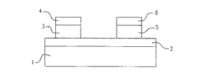
従来より、発光装置を静電的な損傷から防ぐため、パッケージ化の際には図1に示すように、発光ダイオードをツェナーダイオード50のような回路保護ユニットに逆平行に接合している。ツェナーダイオード50によって静電気が放電され、発光装置の損傷が防止できる。しかしながら、回路保護ユニットは、パッケージ処理の間、発光装置と電気的に接続する必要があり、パッケージ化前には、発光装置は回路保護ユニットによって保護されない。特に発光装置のチップ製作処理中は、発光装置は回路保護ユニットで適切に保護されないことになる。また前述の発光装置のパッケージ処理は複雑であり、製作コストがかかる。
Conventionally, in order to prevent the light emitting device from being electrostatically damaged, the light emitting diode is joined in antiparallel to a circuit protection unit such as a Zener
米国特許出願第20020179941号には、静電的な損傷から保護することのできる発光装置が示されている。図2に示すように、発光ダイオードには、ドープされたシリコン系のシャントダイオードが電気的に接続される。静電的な放電の間、シャントダイオードによって、放電電流がドープされたシリコン系のシャントダイオードに流れ、放電電流が発光ダイオードに流れることを防止できる。しかしこの場合も、発光ダイオードチップは、ダイスカット後にシャントダイオードにハンダ付けされるため、発光ダイオードの製作中の静電的な放電による損傷は回避することができない。さらに製作処理工程には、発光ダイオードをシャントダイオードに接続するという追加の手順が必要となり、これは比較的コスト高となる。 U.S. Patent Application No. 20020179941 shows a light emitting device that can be protected from electrostatic damage. As shown in FIG. 2, a doped silicon-based shunt diode is electrically connected to the light emitting diode. During electrostatic discharge, the shunt diode can prevent the discharge current from flowing into the doped silicon-based shunt diode and the discharge current from flowing into the light emitting diode. However, in this case as well, since the light emitting diode chip is soldered to the shunt diode after dicing, damage due to electrostatic discharge during manufacture of the light emitting diode cannot be avoided. Further, the fabrication process requires an additional procedure of connecting the light emitting diode to the shunt diode, which is relatively expensive.
米国特許第6,023,076号には、窒化物系の発光ダイオードが示されている。発光ダイオードの第1の電極は、第1の半導体層および第2の半導体層に接続される。第1の電極と第2の半導体層の間には、ショットキー接合が形成される。逆平行が生じた場合、第1の電極から第2の半導体層、さらには第2の電極側に電流が流れ、発光ダイオード側に電流は流れないため、損傷が回避できる。しかし第2の半導体層は、逆方向に電流を流すためのチャンネルとして使用される。従って、発光ダイオードに逆電流が流れ、逆電流が大きくなった場合、発光ダイオードが損傷を受ける可能性がある。
本発明は、このような課題に鑑みなされたものであり、静電的な損傷を防止することのできる、回路保護ユニットを備える発光装置を提供することを課題とする。 This invention is made | formed in view of such a subject, and makes it a subject to provide a light-emitting device provided with the circuit protection unit which can prevent an electrostatic damage.
本発明は、回路保護ユニットを備える発光装置を提供する。回路保護ユニットは、低抵抗層および保護バリア層を有する。低抵抗層と保護バリア層の界面には、バリア電位が存在する。界面は、ショットキー接合またはp−n接合であっても良い。低抵抗層と保護バリア層の間のバリア電位としては、以下の組み合わせがあり得る。
1.低抵抗層材料は、仕事関数がΦLの金属であり、電位バリア層は、仕事関数がΦBのn型半導体材料であり、ΦL>ΦBとして、バリア電位=ΦL−ΦBである。
2.低抵抗層材料は、仕事関数がΦLの金属であり、電位バリア層は、仕事関数がΦBのp型半導体材料であり、ΦL<ΦBとして、バリア電位=ΦB−ΦLである。
3.低抵抗層材料は、仕事関数がΦLの透明導電性酸化物層(TCO)、例えばITO、CTO、Zn2SnO4、ZnSnO3、MgIn2O4、Zn2In2O5、In4Sn3O12、AgInO2SnまたはIn2O3Znおよび他の半導体化合物であり、電位バリア層は、仕事関数がΦBのn型半導体材料であり、ΦL>ΦBとして、バリア電位=ΦL−ΦBである。
4.低抵抗層材料は、仕事関数がΦLの透明導電性酸化物層であり、電位バリア層は、仕事関数がΦBのp型半導体材料であり、ΦL<ΦBとして、バリア電位=ΦB−ΦLである。
5.低抵抗層材料は、仕事関数がΦLのn型半導体材料であり、電位バリア層は、仕事関数がΦBのp型半導体材料であり、ΦL<ΦBとして、バリア電位=ΦB−ΦLである。
The present invention provides a light emitting device including a circuit protection unit. The circuit protection unit has a low resistance layer and a protective barrier layer. A barrier potential exists at the interface between the low resistance layer and the protective barrier layer. The interface may be a Schottky junction or a pn junction. The barrier potential between the low resistance layer and the protective barrier layer may have the following combinations.
1. The low resistance layer material is a metal having a work function of ΦL, and the potential barrier layer is an n-type semiconductor material having a work function of ΦB, where ΦL> ΦB and the barrier potential = ΦL−ΦB.
2. The low resistance layer material is a metal having a work function of ΦL, and the potential barrier layer is a p-type semiconductor material having a work function of ΦB, where ΦL <ΦB and the barrier potential = ΦB−ΦL.
3. The low resistance layer material is a transparent conductive oxide layer (TCO) having a work function of ΦL, such as ITO, CTO, Zn 2 SnO 4 , ZnSnO 3 , MgIn 2 O 4 , Zn 2 In 2 O 5 , In 4 Sn 3 O 12 , AgInO 2 Sn or In 2 O 3 Zn and other semiconductor compounds, the potential barrier layer is an n-type semiconductor material with a work function of ΦB, and ΦL> ΦB, and the barrier potential = ΦL−ΦB .
Four. The low-resistance layer material is a transparent conductive oxide layer having a work function of ΦL, and the potential barrier layer is a p-type semiconductor material having a work function of ΦB, where ΦL <ΦB and the barrier potential = ΦB−ΦL. .
Five. The low-resistance layer material is an n-type semiconductor material having a work function of ΦL, and the potential barrier layer is a p-type semiconductor material having a work function of ΦB, where ΦL <ΦB and the barrier potential = ΦB−ΦL.
上述の低抵抗層と電位バリア層の組み合わせによって、回路保護ユニットの順方向閾値電圧は高く、回路保護ユニットの逆方向ブレークダウン電圧は低くなる。整流機能を有する回路保護ユニットは、発光装置と一体化され、静電放電または過度の順方向電流によって生じる損傷が防止され、あるいは効果的に抑制される。 By the combination of the low resistance layer and the potential barrier layer, the forward threshold voltage of the circuit protection unit is high, and the reverse breakdown voltage of the circuit protection unit is low. The circuit protection unit having a rectifying function is integrated with the light emitting device, and damage caused by electrostatic discharge or excessive forward current is prevented or effectively suppressed.
特に、回路保護ユニットの順方向バイアス電圧およびブレークダウン電圧は、それぞれVsfおよびVsrで表される。発光装置の順方向作動電圧、順方向損傷電圧およびブレークダウン電圧は、それぞれVf、Vfd、Vrで表され、Vf<|Vsf|<Vfd、|Vsr|<|Vr|である。発光装置が順方向作動電圧Vfで駆動され、順方向作動電圧がVf<|Vsf|である場合、回路保護ユニットは停止される。発光装置が、Vfdよりも高い順方向作動電圧で駆動される場合、|Vsf|<Vfdのため、回路保護ユニットが作動する。そのため、順方向電流が過度に流れることが回避されて、発光装置の損傷が防止され、回路保護ユニットによって発光装置が保護される。一方、発光装置が、逆方向作動電圧によって駆動される場合、|Vsr|<|Vr|のため、逆方向作動電圧がVrに達する前に、回路保護ユニットが作動する(逆方向作動電圧=Vsr)。その結果、逆方向電流が過度に流れることが回避されて、発光装置の損傷が防止され、回路保護ユニットによって発光装置が保護される。 In particular, the forward bias voltage and breakdown voltage of the circuit protection unit are represented by Vsf and Vsr, respectively. The forward operating voltage, forward damage voltage, and breakdown voltage of the light emitting device are represented by Vf, Vfd, and Vr, respectively, and Vf <| Vsf | <Vfd, | Vsr | <| Vr |. When the light emitting device is driven with the forward operating voltage Vf and the forward operating voltage is Vf <| Vsf |, the circuit protection unit is stopped. When the light emitting device is driven with a forward operating voltage higher than Vfd, the circuit protection unit is activated because | Vsf | <Vfd. For this reason, excessive forward current is avoided, damage to the light emitting device is prevented, and the light emitting device is protected by the circuit protection unit. On the other hand, when the light emitting device is driven by the reverse operation voltage, the circuit protection unit is activated before the reverse operation voltage reaches Vr because of | Vsr | <| Vr | (reverse operation voltage = Vsr ). As a result, excessive reverse current is avoided, damage to the light emitting device is prevented, and the light emitting device is protected by the circuit protection unit.
さらに、本発明の回路保護ユニットは、従来のチップ製作処理工程で製作することができる。パッケージ処理時に、ツェナーダイオードまたはシャントダイオードを発光ダイオードに結合する必要ない。また、本発明の回路保護ユニットを備える発光ダイオードは、フリップチップタイプの発光装置であっても良く、この場合ツェナーダイオードが省略され、製作容易性が高まり、コストを抑制することができる。 Furthermore, the circuit protection unit of the present invention can be manufactured by a conventional chip manufacturing process. There is no need to couple a Zener diode or shunt diode to the light emitting diode during packaging. In addition, the light-emitting diode including the circuit protection unit of the present invention may be a flip-chip type light-emitting device. In this case, the Zener diode is omitted, the ease of manufacturing is increased, and the cost can be suppressed.
また、本発明の発光ダイオードは、製作中の静電的な損傷を防止できる回路保護ユニットを備える。そのため、静電放電の抑制という、厳しい要求仕様を緩和することができる。さらに、発光ダイオードの歩留まりが著しく向上する。 In addition, the light emitting diode of the present invention includes a circuit protection unit that can prevent electrostatic damage during manufacture. For this reason, it is possible to relax strict required specifications such as suppression of electrostatic discharge. Furthermore, the yield of light emitting diodes is significantly improved.
本発明は、回路保護ユニットを備える発光装置に関する。発光装置は、第1の表面および第2の表面を有する発光スタッキング層と、回路保護ユニットとを有する。また、回路保護ユニットは、低抵抗層および電位バリア層を有し、低抵抗層と電位バリア層の界面にはバリア電位が存在する。回路保護ユニットは、発光スタッキング層の第1の表面および第2の表面の各々との間で電気的な接続を形成し、整流機能が提供される。 The present invention relates to a light emitting device including a circuit protection unit. The light emitting device includes a light emitting stacking layer having a first surface and a second surface, and a circuit protection unit. The circuit protection unit has a low resistance layer and a potential barrier layer, and a barrier potential exists at the interface between the low resistance layer and the potential barrier layer. The circuit protection unit forms an electrical connection with each of the first surface and the second surface of the light emitting stacking layer to provide a rectifying function.
本発明による発光ダイオードでは、第1の表面と第2の表面は、発光スタッキング層の同じ側に設けられる。また、第1の表面と第2の表面は、発光スタッキング層の反対の側(例えば前面と背面)に設置することも可能である。 In the light emitting diode according to the present invention, the first surface and the second surface are provided on the same side of the light emitting stacking layer. In addition, the first surface and the second surface can be disposed on opposite sides (for example, the front surface and the back surface) of the light emitting stacking layer.
本発明の発光ダイオードでは、低抵抗層と電位バリア層の界面は、ショットキー接合またはp−n接合であっても良い。 In the light emitting diode of the present invention, the interface between the low resistance layer and the potential barrier layer may be a Schottky junction or a pn junction.
本発明の実施例では、低抵抗層の材料には、Ni/Au、NiO/Au、TiWN、ITO、CTO、SnO4Sb、ZnSnO3、In4Sn3O12、Zn2SnO4または他の同等の材料が含まれる。 In an embodiment of the present invention, the material of the low resistance layer may be Ni / Au, NiO / Au, TiWN, ITO, CTO, SnO 4 Sb, ZnSnO 3 , In 4 Sn 3 O 12 , Zn 2 SnO 4 or other Equivalent materials are included.
本発明の実施例では、電位バリア層の材料には、TiO2、SrTiO3、MnTiO3、BaTiO3、ZrO2、Nb2O5、KTaO3、WO3、Fe2O3、ZnO、SnO2、GaP、Si、SiC、CdSe、CdSまたは他の同等の材料が含まれる。 In the embodiment of the present invention, the material of the potential barrier layer includes TiO 2 , SrTiO 3 , MnTiO 3 , BaTiO 3 , ZrO 2 , Nb 2 O 5 , KTaO 3 , WO 3 , Fe 2 O 3 , ZnO, SnO 2. , GaP, Si, SiC, CdSe, CdS or other equivalent materials.
本発明の実施例では、電位バリア層には、Mg、Zn、Be、Crまたは他の同等な材料のようなp型ドーパントが含まれる。本発明の別の実施例では、電位バリア層には、Si、Ge、Sn、Te、O、S、Cまたは他の同等な材料のようなn型ドーパントが含まれる。 In embodiments of the present invention, the potential barrier layer includes a p-type dopant such as Mg, Zn, Be, Cr or other equivalent material. In another embodiment of the present invention, the potential barrier layer includes an n-type dopant such as Si, Ge, Sn, Te, O, S, C, or other equivalent material.
本発明の発光ダイオードは、第1のスタッキング層、発光層および第1の表面を有する第2のスタッキング層を有する。第1のスタッキング層は、第2の表面層を有する。発光層は、第1のスタッキング層の上に形成される。また、第2のスタッキング層は、発光層の上に形成される。第1のスタッキング層の材料には、AlInP、GaN、AlGaN、InGaNまたは他の同等の材料が含まれる。発光層の材料は、AlGaInP、GaN、InGaN、AlInGaNまたは他の同等の材料のような、GaN系のIII−N族から選択される化合物を含む。第2のスタッキング層の材料は、GaN、AlGaN、InGaN、AlInPまたは他の同等の材料のような、GaN系のIII−N族から選択される化合物を含む。 The light emitting diode of the present invention has a first stacking layer, a light emitting layer, and a second stacking layer having a first surface. The first stacking layer has a second surface layer. The light emitting layer is formed on the first stacking layer. The second stacking layer is formed on the light emitting layer. The material of the first stacking layer includes AlInP, GaN, AlGaN, InGaN or other equivalent material. The material of the light emitting layer includes a compound selected from the GaN-based III-N group, such as AlGaInP, GaN, InGaN, AlInGaN or other equivalent materials. The material of the second stacking layer includes a compound selected from a GaN-based group III-N, such as GaN, AlGaN, InGaN, AlInP, or other equivalent material.
回路保護ユニットは、第1の表面の第1の接触領域に設置される。回路保護ユニットの低抵抗層は、第1の表面と接し、電気的に第2の表面と接する。 The circuit protection unit is installed in the first contact area on the first surface. The low resistance layer of the circuit protection unit is in contact with the first surface and electrically in contact with the second surface.
さらに発光装置は、第2の表面の接触領域に設置された第2の回路保護ユニットを有する。第2の回路保護ユニットは、第2の低抵抗層と第2の電位バリア層とを有する。第2の低抵抗層と第2の電位バリア層の界面は、ショットキー接合またはp-n接合であっても良い。第2の低抵抗層は、第2の表面と接する。 Furthermore, the light emitting device has a second circuit protection unit installed in the contact area of the second surface. The second circuit protection unit includes a second low resistance layer and a second potential barrier layer. The interface between the second low resistance layer and the second potential barrier layer may be a Schottky junction or a pn junction. The second low resistance layer is in contact with the second surface.
第2の低抵抗層の材料には、Ni/Au、NiO/Au、TiWN、TCO、ITO、CTO、SnO2Sb、ZnSnO3、Zn2SnO4または他の同等の材料が含まれる。 The material of the second low resistance layer includes Ni / Au, NiO / Au, TiWN, TCO, ITO, CTO, SnO 2 Sb, ZnSnO 3 , Zn 2 SnO 4 or other equivalent materials.
第2の電位バリア層の材料には、TiO2、SrTiO3、MnTiO3、BaTiO3、ZrO2、Nb2O5、KTaO3、WO3、Fe2O3、ZnO、SnO2、GaP、Si、SiC、CdSe、CdSまたは他の同等の材料が含まれる。
The material of the second potential barrier layer, TiO 2, SrTiO 3, MnTiO 3, BaTiO 3,
本発明の実施例では、第2の電位バリア層には、Mg、Zn、Be、Crまたは他の同等な材料のようなp型ドーパントが含まれる。本発明の別の実施例では、第2の電位バリア層には、Si、Ge、Sn、Te、O、S、Cまたは他の同等な材料のようなn型ドーパントが含まれる。 In an embodiment of the invention, the second potential barrier layer includes a p-type dopant such as Mg, Zn, Be, Cr or other equivalent material. In another embodiment of the present invention, the second potential barrier layer includes an n-type dopant such as Si, Ge, Sn, Te, O, S, C, or other equivalent material.
さらに本発明の発光装置は、第1の表面の第2の接触領域に設置された第1の電極と、第2の表面の第2の接触領域に設置された第2の電極とを有する。回路保護ユニットと第1の電極は、電気的に接続される。また第2の回路保護ユニットと第2の電極も、電気的に接続される。 Furthermore, the light-emitting device of the present invention includes a first electrode disposed in the second contact region on the first surface, and a second electrode disposed in the second contact region on the second surface. The circuit protection unit and the first electrode are electrically connected. The second circuit protection unit and the second electrode are also electrically connected.
前述の本発明の発光装置では、低抵抗層は、発光スタッキング層の第1の表面上に設置される。また第1の電極は、低抵抗層の第1の接触領域に設置される。電位バリア層は、低抵抗層の第2の接触領域に設置される。 In the light emitting device of the present invention described above, the low resistance layer is disposed on the first surface of the light emitting stacking layer. The first electrode is disposed in the first contact region of the low resistance layer. The potential barrier layer is disposed in the second contact region of the low resistance layer.
前述の本発明の発光装置では、第2の低抵抗層は、発光スタッキング層の第2の表面上に設置される。また、第2の電極は、第2の低抵抗層の第1の接触領域に設置される。電位バリア層は、第2の低抵抗層の第2の領域に設置される。 In the light emitting device of the present invention described above, the second low resistance layer is disposed on the second surface of the light emitting stacking layer. Further, the second electrode is disposed in the first contact region of the second low resistance layer. The potential barrier layer is disposed in the second region of the second low resistance layer.
さらに本発明の発光装置は、回路保護ユニットまたは第2の回路保護ユニット上に設置された、複数の他の回路保護ユニットを有する。 Furthermore, the light-emitting device of the present invention has a plurality of other circuit protection units installed on the circuit protection unit or the second circuit protection unit.
図面は、本発明を示す明細書の一部として添付され、記載の内容とともに、本発明の原理を説明する際に用いられ、当業者が本発明を実施することができる程度に記載されている。 The drawings are included as part of the specification illustrating the present invention, and together with the description are used to explain the principles of the invention and are described to the extent that those skilled in the art can practice the invention. .
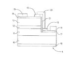
図3には、本発明の好適実施例による回路保護ユニットを備える発光装置1が示されており、この発光装置1は、基板10、第1のスタッキング層11、発光層12、第2のスタッキング層13、第1の低抵抗層14、第1の電極15、第1の電位バリア層16、第2の低抵抗層17、第2の電極18、第2の電位バリア層19および電気接続層20を有する。本実施例では、第1のスタッキング層11は、基板10に設置され、第1のスタッキング層11は、第1のエピタキシャル領域と第2の表面領域を有する。発光層12は、第1のエピタキシャル領域に設置され、第2のスタッキング層13は、発光層12の上に設置される。また、第1の低抵抗層14は、第2のスタッキング層13の上に設置され、第1の低抵抗層14は、第1の接触領域と第2の接触領域を有する。第1の電極15は、第1の接触領域に設置され、第1の低抵抗層14と第1の電極15間にはオーム接続が生じる。さらに、第1の電位バリア層16は、第2の接触領域に設置され、第1の低抵抗層14と電位バリア層16の界面には、バリア電位が存在する。第1の低抵抗層14と第1の電位バリア層16の界面は、ショットキー接合またはp−n接合とすることができる。第2の低抵抗層17は、第2の表面領域に設置され、第2の低抵抗層17は、第3の接触領域および第4の接触領域を有する。第2の電極18は、第3の接触領域に設置され、第2の低抵抗層17と第2の電極18の界面にはオーム接続が形成される。また、第2の電位バリア層19は、第4の接触領域に設置され、第2の低抵抗層17と第2の電位バリア層19の界面にはバリア電位が存在する。第2の低抵抗層17と第2の電位バリア層19の界面は、ショットキー接合またはp-n接合とすることができる。電気接続層20は、第1の電位バリア層16と第2の電位バリア層19を電気的に接続し、電気接続層20、第1の電位バリア層16および第2の電位バリア層19によって、回路保護ユニットが形成される。第1のスタッキング層11、発光層12および第2のスタッキング層13の一部を覆うように絶縁層21が形成され、電気接続層20は、第1のスタッキング層11、発光層12および第2のスタッキング層13から電気的に絶縁される。
FIG. 3 shows a light-emitting
発光装置1は、低抵抗層14および第1の電位バリア層16のみを含んでも良い。本発明の別の実施例では、発光装置1は、低抵抗層14、第1の電位保護層16、第2の低抵抗層17および第2の電位バリア層19を有する。図5には、図4に示す回路保護ユニットの電流―電圧曲線を示す。図5において、破線は、低抵抗層2、第1の電位バリア層3および第1の電極4で構成される図4に示す回路保護ユニットの電流−電圧曲線を示す。低抵抗層2の材料は、インジウムスズ酸化物(ITO)である。第1の電位バリア層16材料は、Crがドープされたp型の酸化チタンである。図5の実線は、低抵抗層2、第1の電位バリア層3、第1の電極4、第2の電位バリア層5および第2の電極6で構成される図4に示す回路保護ユニットの電流―電圧曲線を示す。図5に従って、全順方向バイアスと逆方向レークダウン電圧を制御する回路保護ユニットの数を変更することは、当業者には容易に想定される。従って、複数の低抵抗層および電位バリア層を、第1の電位バリア層16および/または第2の電位バリア層19に組み合わせて使用することにより、ユーザーの要求に適合させることができる。
The
図6には、本発明の第2の実施例による、回路保護ユニットを備える第2の発光装置2が示されている。図3および図6において、同一符号は同じ構成物を示していることに留意する必要がある。従って、これらの構成物に関する説明は省略する。本発明の第2の実施例の第2の発光装置2では、第2のスタッキング層13は、第1の接触領域および第2の接触領域を有する。第2のスタッキング層13の第1の接触領域には、第1のオーム接続層24が形成される。第1の電極15は、第1のオーム接続層24の上に設置され、第1のオーム接続層24と第1の電極の界面には、オーム接続が形成される。第2の表面は、第3の接触領域および第4の接触領域を有する。第2のオーム接続層27は、第3の接触領域に設置される。第2の電極18は、第2のオーム接続層27の上に設置され、第2のオーム層27と第2の電極18の界面には、オーム接続が形成される。第2の接触領域の上部、第1のスタッキング層11および発光層12および第2のスタッキング層13の側壁、ならびに第4の接触領域の上部には、電気的絶縁のため絶縁層31が形成される。第1の低抵抗層28は、第5の接触領域および第6の接触領域を有する。第1の電位バリア層16は、第5の接触領域に設置される。第1の低抵抗層28と電位バリア層16の界面には、バリア電位が存在する。第1の低抵抗層28と第1の電位バリア層16の界面は、ショットキー接合またはp−n接合とすることができる。第2の電位バリア層19は、第6の接触領域に設置され、第1の低抵抗層28と第2の電位バリア層19の界面には、バリア電位が存在する。第1の低抵抗層28と第2の電位バリア層19の界面は、ショットキー接合またはp−n接合とすることができる。第1の低抵抗層28は、第1の電位バリア層16および第2の電位バリア層19と電気的に接続され、回路保護ユニットが形成される。第1の電気接続層29は、第1の電極15と第1の電位バリア層16を電気的に接続する。第2の電気接続層30は、第2の電極18と第2の電位バリア層19を電気的に接続する。
FIG. 6 shows a second
本発明では、第2の発光装置2は、第1の低抵抗層28と第1の電位バリア層16のみを含む。本発明の別の実施例では、第2の発光装置2は、第1の低抵抗層28、第1の電位バリア層16、第1の低抵抗層28および第2の電位保護層19を有する。本発明の別の実施例では、複数の低抵抗層および電位バリア層が、第1の電位バリア層16および/または第2の電位バリア層19の上に設置され、ユーザーの要求が満たされる。
In the present invention, the second
図7には、本発明の第3の実施例による、回路保護ユニットを備える第3の発光装置3を示す。図3および図7において、同一の参照符号は、同じ構成物を表していることに留意する必要がある。従って、これらの構成物に関する説明は、ここでは省略する。図7の発光装置3には、基板と第1のスタッキング層11の間に、結合層301が設けられる。第1のスタッキング層11は、接合技術により、基板10に結合される。
FIG. 7 shows a third light-emitting device 3 including a circuit protection unit according to the third embodiment of the present invention. It should be noted that in FIG. 3 and FIG. 7, the same reference numerals represent the same components. Therefore, the description regarding these components is omitted here. In the light emitting device 3 of FIG. 7, a
本発明の別の実施例では、基板10と第1のスタッキング層11は、結合層301を使用せずに、高温高圧下で直接結合される。基板10と第1のスタッキング層11が高温高圧下で直接結合されてから、発光装置の反対の側に、第1の電極および第2の電極が設置される。回路保護ユニットの構造は、後述する。
In another embodiment of the present invention, the
第3の発光装置3の回路保護ユニットおよび電極配置は、第2の発光装置2の回路保護ユニットおよび電極配置と同じである。
The circuit protection unit and electrode arrangement of the third light emitting device 3 are the same as the circuit protection unit and electrode arrangement of the second
図8には、本発明の第4の実施例による回路保護ユニットを備える第4の発光装置4が示されている。図3と図8において、同一の参照符号は、同じ構成物を表していることに留意する必要がある。従って、これらの構成物に関する説明は、ここでは省略する。第4の発光装置4では、図3に示す基板10の代わりに導電性基板40が用いられる。また導電性基板40の下側表面に設置された第2の電極48は、図3に示す第1の電極18の代わりに使用される。導電性基板40および第2の電極を備える第4の発光装置4は、垂直配置構造のLEDである。
FIG. 8 shows a fourth light-emitting device 4 including a circuit protection unit according to the fourth embodiment of the present invention. It should be noted that the same reference numerals in FIG. 3 and FIG. 8 represent the same components. Therefore, the description regarding these components is omitted here. In the fourth light emitting device 4, a conductive substrate 40 is used instead of the
第4の発光装置4では、第2の低抵抗層17および第2の電位バリア層19が、第1のスタッキング層11の上に設置される。別の言い方では、第1のスタッキング層11および第2の電極48は、導電性基板40の反対の側に設置される。また、第1の電位バリア層16および第2の電位バリア層19は、電気接続層20によって、相互に電気的に接続される。
In the fourth light emitting device 4, the second
本発明の別の実施例では、第4の発光装置4は、第1の低抵抗層28と、第1の電位バリア層16のみを有する。回路保護ユニットは、第1の電位バリア層16および第2の電極48を電気的に接続することにより構成される。
In another embodiment of the present invention, the fourth light emitting device 4 has only the first
第1の電位バリア層16および第2の電位バリア層19は、n型層またはp型層であっても良い。Mg、Zn、Beまたは他の同等のドーパントが用いられる場合、第1の電位バリア層16および第2の電位バリア層19は、p型層である。Si、Ge、Sn、Te、O、S、Cまたは他の同等のドーパントが用いられる場合、第1の電位バリア層16および第2の電位バリア層19は、n型層である。第1の低抵抗層28の材料には、Ni/Au、NiO/Au、TiWN、TCO、ITO、CTO、SnO2Sb、ZnSnO3、In4Sn3O12、Zn2SnO4または他の同等の材料が含まれる。第2の低抵抗層17の材料には、Ni/Au、NiO/Au、TiWN、TCO、ITO、CTO、SnO2Sb、ZnSnO3、Zn2SnO4または他の同等の材料が含まれる。第1のオーム接続層24の材料には、Ni/Au、NiO/Au、TiWN、TCO、ITO、CTO、SnO2Sb、ZnSnO3、Zn2SnO4または他の同等の材料が含まれる。第2のオーム接続層の材料には、Ni/Au、NiO/Au、TiWN、TCO、ITO、CTO、SnO2Sb、ZnSnO3、Zn2SnO4または他の同等の材料が含まれる。第1の電位バリア層16は、p型ドーパントまたはn型ドーパントを含む層である。電位バリア層の材料には、TiO2、SrTiO3、FeTiO3、MnTiO3、BaTiO3、ZrO2、Nb2O5、KTaO3、WO3、ZnO、SnO2、GaP、Si、SiC、CdSe、CdSまたは他の同等の材料が含まれる。第2の電位バリア層19は、p型のドーパントまたはn型のドーパントを含む層である。電位バリア層の材料には、TiO2、SrTiO3、FeTiO3、MnTiO3、BaTiO3、ZrO2、Nb2O5、KTaO3、WO3、ZnO、SnO2、GaP、Si、SiC、CdSe、CdSまたは他の同等の材料が含まれる。第1のスタッキング層11の材料は、AlInP、GaN、AlGaN、InGaNまたは他の同等の材料のような群に属する化合物を含む。発光層12の材料には、AlGaInP、GaN、InGaNまたはAlInGaNのような、III-V族の窒化物系半導体材料が含まれる。第2のスタッキング層13の材料には、AlGaInP、GaN、AlInGaNおよびInGaNのような、GaN系のIII-N族の化合物が含まれる。バリア層19には、SiNx、SiO2または他の同等の材料が含まれる。電気接続層20の材料には、Cr/Au、Ni/Au、Cr/Al、Ti/Al、Ti/Auまたは他の同等の材料が含まれる。第1の電気接続層29の材料には、Cr/Au、Ni/Au、Cr/Al、Ti/Al、Ti/Auまたは他の同等の材料が含まれる。第2の電気接続層30の材料には、Cr/Au、Ni/Au、Cr/Al、Ti/Al、Ti/Auまたは他の同等の材料が含まれる。電気接続層20の材料には、ポリイミド、BCB、PFBCまたは他の同等の材料が含まれる。導電性基板40の材料には、GaP、SiCまたは他の同等の材料が含まれる。ウェハ接合技術には、接着による接合、金属ハンダ付けおよび直接接合技術が含まれる。
The first
本発明についていくつかの実施例を示したが、本発明の構成に関して、本発明の範囲および思想から逸脱しないで、多くの変更や修正が当業者には可能である。このような観点から、請求項およびこれと等価な範囲にある、上述の発明の変更や修正は、本発明に属するものである。 While several embodiments of the present invention have been shown, many changes and modifications can be made by those skilled in the art without departing from the scope and spirit of the present invention with respect to the structure of the present invention. From this point of view, changes and modifications of the above-described invention within the scope of the claims and the equivalent scope thereof belong to the present invention.
1 発光装置
2 第2の発光装置
3 第3の発光装置
4 第4の発光装置
10 基板
11 第1のスタッキング層
12 発光層
13 第2のスタッキング層
14 第1の低抵抗層
15 第1の電極
16 第1の電位バリア層
17 第2の低抵抗層
18 第2の電極
19 第2の電位バリア層
20 電気接続層
24 第1のオーム接続層
27 第2のオーム接続層
28 第1の低抵抗層
29 第1の電気接続層
30 第2の電気接続層
31 絶縁層
40 導電性基板
48 第2の電極
301 結合層
DESCRIPTION OF
Claims (17)
第1の表面と第2の表面を有する発光スタッキング層であって、前記第2の表面を有する第1の半導体層と、前記第1の半導体層上に形成される発光層と、前記第1の表面を有し、前記発光層上に形成される第2の半導体層とを含む、発光スタッキング層と、
前記第1の表面と前記第2の表面の何れかに位置し、前記第1の表面と前記第2の表面にそれぞれ電気的に接続されて整流機能を提供する少なくとも一つの回路保護ユニットと、
を含み、
前記回路保護ユニットは、第1の抵抗層と第1の電位バリア層とを有し、前記第1の抵抗層と前記第1の電位バリア層との間の界面には、バリア電位が存在し、
前記第1の抵抗層と前記第1の電位バリア層との間の界面は、ショットキー界面又はp−n界面であり、
前記回路保護ユニットは、前記第1の表面と前記第2の表面に電気的に接続される電気接続層を更に含み、
前記回路保護ユニットは、前記第1の表面と前記第2の表面の他の表面に位置する第2の抵抗層と第2の電位バリア層を更に含む、発光装置。 A light emitting device having a circuit protection unit,
A light emitting stacking layer having a first surface and a second surface, the first semiconductor layer having the second surface, the light emitting layer formed on the first semiconductor layer, and the first A light-emitting stacking layer comprising a second semiconductor layer formed on the light-emitting layer,
At least one circuit protection unit located on either the first surface or the second surface and electrically connected to the first surface and the second surface, respectively, to provide a rectifying function;
Including
The circuit protection unit includes a first resistance layer and a first potential barrier layer, and a barrier potential exists at an interface between the first resistance layer and the first potential barrier layer. ,
The interface between the first resistance layer and the first potential barrier layer is a Schottky interface or a pn interface;
The circuit protection unit further seen including an electrical connection layer electrically connected to said first surface said second surface,
The circuit protection unit further includes a second resistance layer and a second potential barrier layer located on another surface of the first surface and the second surface .
前記第1の抵抗層は、金属又は透明導電性酸化物であり、且つ、前記第1の電位バリア層は、n型半導体であるときに、ΦL>ΦBであり、
前記第1の抵抗層は、金属又は透明導電性酸化物であり、且つ、前記第1の電位バリア層は、p型半導体であるときに、ΦL<ΦBであり、
前記第1の抵抗層は、n型半導体であり、且つ、前記第1の電位パリア層は、p型半導体であるときに、ΦL<ΦBである、請求項1に記載の発光装置。 The first resistance layer has a work function ΦL, the first potential barrier layer has a work function ΦB,
When the first resistance layer is a metal or a transparent conductive oxide, and the first potential barrier layer is an n-type semiconductor, ΦL> ΦB,
When the first resistance layer is a metal or a transparent conductive oxide, and the first potential barrier layer is a p-type semiconductor, ΦL <ΦB,
2. The light emitting device according to claim 1, wherein when the first resistance layer is an n-type semiconductor and the first potential barrier layer is a p-type semiconductor, ΦL <ΦB.
Applications Claiming Priority (2)
| Application Number | Priority Date | Filing Date | Title |
|---|---|---|---|
| TW093130813 | 2004-10-08 | ||
| TW093130813A TWI244748B (en) | 2004-10-08 | 2004-10-08 | A light-emitting device with a protecting structure |
Publications (3)
| Publication Number | Publication Date |
|---|---|
| JP2006108682A JP2006108682A (en) | 2006-04-20 |
| JP2006108682A5 JP2006108682A5 (en) | 2008-11-20 |
| JP5336030B2 true JP5336030B2 (en) | 2013-11-06 |
Family
ID=36120746
Family Applications (1)
| Application Number | Title | Priority Date | Filing Date |
|---|---|---|---|
| JP2005291277A Expired - Fee Related JP5336030B2 (en) | 2004-10-08 | 2005-10-04 | Light emitting device having a circuit protection unit |
Country Status (5)
| Country | Link |
|---|---|
| US (1) | US7683383B2 (en) |
| JP (1) | JP5336030B2 (en) |
| KR (1) | KR101056457B1 (en) |
| DE (1) | DE102005043649A1 (en) |
| TW (1) | TWI244748B (en) |
Families Citing this family (31)
| Publication number | Priority date | Publication date | Assignee | Title |
|---|---|---|---|---|
| KR100833313B1 (en) * | 2006-01-02 | 2008-05-28 | 삼성전기주식회사 | GaN TYPE LIGHT EMITTING DIODE DEVICE AND METHOD OF MANUFACTURING THE SAME |
| JP4694395B2 (en) * | 2006-03-22 | 2011-06-08 | 日本オプネクスト株式会社 | Nitride semiconductor light emitting device and manufacturing method thereof |
| US7994514B2 (en) * | 2006-04-21 | 2011-08-09 | Koninklijke Philips Electronics N.V. | Semiconductor light emitting device with integrated electronic components |
| GB2439358B (en) * | 2006-06-19 | 2010-12-15 | Cambridge Display Tech Ltd | Organic electroluminescent optocouplers |
| US8546818B2 (en) | 2007-06-12 | 2013-10-01 | SemiLEDs Optoelectronics Co., Ltd. | Vertical LED with current-guiding structure |
| US8148733B2 (en) | 2007-06-12 | 2012-04-03 | SemiLEDs Optoelectronics Co., Ltd. | Vertical LED with current guiding structure |
| US7759670B2 (en) * | 2007-06-12 | 2010-07-20 | SemiLEDs Optoelectronics Co., Ltd. | Vertical LED with current guiding structure |
| DE102007057672A1 (en) * | 2007-11-30 | 2009-06-04 | Osram Opto Semiconductors Gmbh | Optoelectronic semiconductor body e.g. thin film-LED chip, for use in headlight i.e. motor vehicle headlight, has Schottky contact formed between extension and n-type layer and operated in reverse direction during operation of active layer |
| KR101438811B1 (en) * | 2008-01-03 | 2014-09-05 | 엘지이노텍 주식회사 | Semiconductor light emitting device and fabrication method thereof |
| KR101457204B1 (en) * | 2008-02-01 | 2014-11-03 | 서울바이오시스 주식회사 | Light emitting device and method for manufacturing thereof |
| US7923744B2 (en) * | 2008-02-22 | 2011-04-12 | Huga Optotech Inc. | Semiconductor light-emitting device |
| TWI371873B (en) * | 2008-02-22 | 2012-09-01 | Huga Optotech Inc | Semiconductor light-emitting device |
| WO2009125953A2 (en) * | 2008-04-06 | 2009-10-15 | Song June O | Luminous element |
| DE102008034560B4 (en) * | 2008-07-24 | 2022-10-27 | OSRAM Opto Semiconductors Gesellschaft mit beschränkter Haftung | Radiation-emitting semiconductor chip and method for producing a radiation-emitting semiconductor chip |
| CN101656260B (en) * | 2009-09-08 | 2011-09-21 | 厦门市三安光电科技有限公司 | Antistatic GaN-based luminescent device and preparation method thereof |
| KR101039896B1 (en) * | 2009-12-03 | 2011-06-09 | 엘지이노텍 주식회사 | Light emitting device and fabrication method thereof |
| KR100999692B1 (en) * | 2010-02-18 | 2010-12-08 | 엘지이노텍 주식회사 | Light emitting device, method for fabricating the light emitting device and light emitting device package |
| KR101028206B1 (en) * | 2010-04-08 | 2011-04-11 | 엘지이노텍 주식회사 | Light emitting device, method for fabricating the same and light emitting device package |
| JP5281612B2 (en) * | 2010-05-26 | 2013-09-04 | 株式会社東芝 | Semiconductor light emitting device and manufacturing method thereof |
| US9548286B2 (en) * | 2010-08-09 | 2017-01-17 | Micron Technology, Inc. | Solid state lights with thermal control elements |
| KR101785644B1 (en) * | 2011-01-26 | 2017-10-16 | 엘지이노텍 주식회사 | Light emitting diode and method for fabricating the light emitting device |
| CN103415935B (en) * | 2011-03-14 | 2016-09-14 | 皇家飞利浦有限公司 | There is the LED redistributing the perpendicular contact part installed for flip-chip |
| US9490239B2 (en) | 2011-08-31 | 2016-11-08 | Micron Technology, Inc. | Solid state transducers with state detection, and associated systems and methods |
| US8809897B2 (en) | 2011-08-31 | 2014-08-19 | Micron Technology, Inc. | Solid state transducer devices, including devices having integrated electrostatic discharge protection, and associated systems and methods |
| KR102085897B1 (en) * | 2013-06-10 | 2020-03-06 | 엘지이노텍 주식회사 | Light emitting device and light emitting device package |
| KR102255196B1 (en) | 2014-02-03 | 2021-05-25 | 삼성디스플레이 주식회사 | Flexible display device and method of fabricating the same |
| KR101553372B1 (en) * | 2014-03-28 | 2015-09-15 | 전북대학교산학협력단 | Self-protective light emitting device |
| KR102224245B1 (en) * | 2015-01-26 | 2021-03-08 | 엘지이노텍 주식회사 | Light emitting device, light emitting package having the same and light system having the same |
| CN109860364B (en) * | 2017-08-30 | 2020-09-01 | 天津三安光电有限公司 | Light emitting diode |
| CN108172668B (en) * | 2018-01-16 | 2020-02-11 | 福建兆元光电有限公司 | Light-emitting diode |
| KR20200075430A (en) | 2018-12-18 | 2020-06-26 | 김은혜 | Customer management card for beauty salon |
Family Cites Families (17)
| Publication number | Priority date | Publication date | Assignee | Title |
|---|---|---|---|---|
| JPH06112525A (en) * | 1992-09-25 | 1994-04-22 | Nisshin Steel Co Ltd | Heterojunction element for light emitting device |
| JPH06267301A (en) * | 1993-03-15 | 1994-09-22 | Olympus Optical Co Ltd | Organic photoluminescence element |
| JPH1065215A (en) | 1996-08-22 | 1998-03-06 | Toyoda Gosei Co Ltd | Iii nitride semiconductor light-emitting device |
| JP3787202B2 (en) * | 1997-01-10 | 2006-06-21 | ローム株式会社 | Semiconductor light emitting device |
| JP3257455B2 (en) * | 1997-07-17 | 2002-02-18 | 松下電器産業株式会社 | Light emitting device |
| JP3914615B2 (en) * | 1997-08-19 | 2007-05-16 | 住友電気工業株式会社 | Semiconductor light emitting device and manufacturing method thereof |
| JPH11298041A (en) * | 1998-04-15 | 1999-10-29 | Toyoda Gosei Co Ltd | Group iii nitride semiconductor light-emitting element and light source device |
| JP2950811B1 (en) * | 1998-05-22 | 1999-09-20 | 株式会社エイ・ティ・アール環境適応通信研究所 | Super lattice semiconductor light emitting device |
| JP3686569B2 (en) * | 2000-03-02 | 2005-08-24 | シャープ株式会社 | Semiconductor light emitting device and display device using the same |
| US6693352B1 (en) | 2000-06-05 | 2004-02-17 | Emitronix Inc. | Contact structure for group III-V semiconductor devices and method of producing the same |
| JP2002368103A (en) | 2001-06-05 | 2002-12-20 | Hitachi Ltd | Semiconductor and manufacturing method therefor |
| JP3791765B2 (en) * | 2001-06-08 | 2006-06-28 | 豊田合成株式会社 | Group III nitride compound semiconductor light emitting device |
| JP2003289176A (en) * | 2002-01-24 | 2003-10-10 | Sony Corp | Semiconductor light emitting element and its manufacturing method |
| TW577184B (en) * | 2002-12-26 | 2004-02-21 | Epistar Corp | Light emitting layer having voltage/resistance interdependent layer |
| TW579610B (en) * | 2003-01-30 | 2004-03-11 | Epistar Corp | Nitride light-emitting device having adhered reflective layer |
| TWI229463B (en) * | 2004-02-02 | 2005-03-11 | South Epitaxy Corp | Light-emitting diode structure with electro-static discharge protection |
| US20050218414A1 (en) * | 2004-03-30 | 2005-10-06 | Tetsuzo Ueda | 4H-polytype gallium nitride-based semiconductor device on a 4H-polytype substrate |
-
2004
- 2004-10-08 TW TW093130813A patent/TWI244748B/en not_active IP Right Cessation
-
2005
- 2005-09-02 KR KR1020050081565A patent/KR101056457B1/en active IP Right Grant
- 2005-09-08 US US11/222,922 patent/US7683383B2/en not_active Expired - Fee Related
- 2005-09-13 DE DE102005043649A patent/DE102005043649A1/en not_active Ceased
- 2005-10-04 JP JP2005291277A patent/JP5336030B2/en not_active Expired - Fee Related
Also Published As
| Publication number | Publication date |
|---|---|
| US20060081857A1 (en) | 2006-04-20 |
| KR101056457B1 (en) | 2011-08-11 |
| TWI244748B (en) | 2005-12-01 |
| DE102005043649A1 (en) | 2006-04-20 |
| JP2006108682A (en) | 2006-04-20 |
| TW200612541A (en) | 2006-04-16 |
| US7683383B2 (en) | 2010-03-23 |
| KR20060050956A (en) | 2006-05-19 |
Similar Documents
| Publication | Publication Date | Title |
|---|---|---|
| JP5336030B2 (en) | Light emitting device having a circuit protection unit | |
| JP4697397B2 (en) | Composite semiconductor device | |
| US7652296B2 (en) | Light emitting device with high light extraction efficiency | |
| JP5466156B2 (en) | Vertical LED with current induction structure | |
| EP2225783B1 (en) | Semiconductor light emitting device | |
| KR101039896B1 (en) | Light emitting device and fabrication method thereof | |
| US6593597B2 (en) | Group III-V element-based LED having ESD protection capacity | |
| JP4577497B2 (en) | Composite semiconductor device of semiconductor light emitting element and protective element | |
| KR101428085B1 (en) | Semiconductor light emitting device and fabrication method thereof | |
| JP4777293B2 (en) | Nitride semiconductor light emitting diode | |
| CN102194847B (en) | Light emitting diode, light emitting diode package, method of manufacturing light emitting diode and lighting system | |
| JP2006086300A (en) | Semiconductor light emitting device with protective element, and its manufacturing method | |
| JP2007043046A (en) | Light-emitting device having protective element | |
| KR100609968B1 (en) | Light emitting diode with the function of electrostatic discharge protection and fabricating method thereof | |
| JP6262856B2 (en) | Optoelectronic semiconductor chip | |
| KR100649642B1 (en) | Compound semiconductor light emitting device having an esd protecting element and method for manufacturing the same | |
| KR102413447B1 (en) | Light emitting device | |
| CN100403561C (en) | Light-emitting component with circuit protection device | |
| EP2086026A2 (en) | Light emitting device with high light extraction efficiency | |
| US8963172B2 (en) | Optical semiconductor device including antiparallel semiconductor light-emitting element and Schottky diode element | |
| EP3188241B1 (en) | Light-emitting diode chip | |
| KR100631907B1 (en) | Gallium nitride based light emitting device with P-N diode for ESD protection | |
| KR101457207B1 (en) | Light emitting diode having electrostatic discharge protect device | |
| KR20140057799A (en) | Light emitting device | |
| KR20110119930A (en) | A light emitting device, a method of fabricating the light emitting device, and a light emitting device package |
Legal Events
| Date | Code | Title | Description |
|---|---|---|---|
| A521 | Request for written amendment filed |
Free format text: JAPANESE INTERMEDIATE CODE: A523 Effective date: 20081003 |
|
| A621 | Written request for application examination |
Free format text: JAPANESE INTERMEDIATE CODE: A621 Effective date: 20081003 |
|
| A977 | Report on retrieval |
Free format text: JAPANESE INTERMEDIATE CODE: A971007 Effective date: 20110801 |
|
| A131 | Notification of reasons for refusal |
Free format text: JAPANESE INTERMEDIATE CODE: A131 Effective date: 20110809 |
|
| A521 | Request for written amendment filed |
Free format text: JAPANESE INTERMEDIATE CODE: A523 Effective date: 20111107 |
|
| A131 | Notification of reasons for refusal |
Free format text: JAPANESE INTERMEDIATE CODE: A131 Effective date: 20120214 |
|
| A02 | Decision of refusal |
Free format text: JAPANESE INTERMEDIATE CODE: A02 Effective date: 20130226 |
|
| A521 | Request for written amendment filed |
Free format text: JAPANESE INTERMEDIATE CODE: A523 Effective date: 20130620 |
|
| A911 | Transfer to examiner for re-examination before appeal (zenchi) |
Free format text: JAPANESE INTERMEDIATE CODE: A911 Effective date: 20130627 |
|
| TRDD | Decision of grant or rejection written | ||
| A01 | Written decision to grant a patent or to grant a registration (utility model) |
Free format text: JAPANESE INTERMEDIATE CODE: A01 Effective date: 20130723 |
|
| A61 | First payment of annual fees (during grant procedure) |
Free format text: JAPANESE INTERMEDIATE CODE: A61 Effective date: 20130801 |
|
| R150 | Certificate of patent or registration of utility model |
Ref document number: 5336030 Country of ref document: JP Free format text: JAPANESE INTERMEDIATE CODE: R150 Free format text: JAPANESE INTERMEDIATE CODE: R150 |
|
| R250 | Receipt of annual fees |
Free format text: JAPANESE INTERMEDIATE CODE: R250 |
|
| R250 | Receipt of annual fees |
Free format text: JAPANESE INTERMEDIATE CODE: R250 |
|
| R250 | Receipt of annual fees |
Free format text: JAPANESE INTERMEDIATE CODE: R250 |
|
| R250 | Receipt of annual fees |
Free format text: JAPANESE INTERMEDIATE CODE: R250 |
|
| R250 | Receipt of annual fees |
Free format text: JAPANESE INTERMEDIATE CODE: R250 |
|
| LAPS | Cancellation because of no payment of annual fees |