JP4932078B2 - Light emitting device and manufacturing method thereof - Google Patents
Light emitting device and manufacturing method thereof Download PDFInfo
- Publication number
- JP4932078B2 JP4932078B2 JP2000368603A JP2000368603A JP4932078B2 JP 4932078 B2 JP4932078 B2 JP 4932078B2 JP 2000368603 A JP2000368603 A JP 2000368603A JP 2000368603 A JP2000368603 A JP 2000368603A JP 4932078 B2 JP4932078 B2 JP 4932078B2
- Authority
- JP
- Japan
- Prior art keywords
- light emitting
- semiconductor light
- emitting element
- emission wavelength
- light
- Prior art date
- Legal status (The legal status is an assumption and is not a legal conclusion. Google has not performed a legal analysis and makes no representation as to the accuracy of the status listed.)
- Expired - Lifetime
Links
Images


Classifications
-
- H—ELECTRICITY
- H01—ELECTRIC ELEMENTS
- H01L—SEMICONDUCTOR DEVICES NOT COVERED BY CLASS H10
- H01L2224/00—Indexing scheme for arrangements for connecting or disconnecting semiconductor or solid-state bodies and methods related thereto as covered by H01L24/00
- H01L2224/01—Means for bonding being attached to, or being formed on, the surface to be connected, e.g. chip-to-package, die-attach, "first-level" interconnects; Manufacturing methods related thereto
- H01L2224/26—Layer connectors, e.g. plate connectors, solder or adhesive layers; Manufacturing methods related thereto
- H01L2224/31—Structure, shape, material or disposition of the layer connectors after the connecting process
- H01L2224/32—Structure, shape, material or disposition of the layer connectors after the connecting process of an individual layer connector
- H01L2224/321—Disposition
- H01L2224/32151—Disposition the layer connector connecting between a semiconductor or solid-state body and an item not being a semiconductor or solid-state body, e.g. chip-to-substrate, chip-to-passive
- H01L2224/32221—Disposition the layer connector connecting between a semiconductor or solid-state body and an item not being a semiconductor or solid-state body, e.g. chip-to-substrate, chip-to-passive the body and the item being stacked
- H01L2224/32225—Disposition the layer connector connecting between a semiconductor or solid-state body and an item not being a semiconductor or solid-state body, e.g. chip-to-substrate, chip-to-passive the body and the item being stacked the item being non-metallic, e.g. insulating substrate with or without metallisation
-
- H—ELECTRICITY
- H01—ELECTRIC ELEMENTS
- H01L—SEMICONDUCTOR DEVICES NOT COVERED BY CLASS H10
- H01L2224/00—Indexing scheme for arrangements for connecting or disconnecting semiconductor or solid-state bodies and methods related thereto as covered by H01L24/00
- H01L2224/01—Means for bonding being attached to, or being formed on, the surface to be connected, e.g. chip-to-package, die-attach, "first-level" interconnects; Manufacturing methods related thereto
- H01L2224/26—Layer connectors, e.g. plate connectors, solder or adhesive layers; Manufacturing methods related thereto
- H01L2224/31—Structure, shape, material or disposition of the layer connectors after the connecting process
- H01L2224/32—Structure, shape, material or disposition of the layer connectors after the connecting process of an individual layer connector
- H01L2224/321—Disposition
- H01L2224/32151—Disposition the layer connector connecting between a semiconductor or solid-state body and an item not being a semiconductor or solid-state body, e.g. chip-to-substrate, chip-to-passive
- H01L2224/32221—Disposition the layer connector connecting between a semiconductor or solid-state body and an item not being a semiconductor or solid-state body, e.g. chip-to-substrate, chip-to-passive the body and the item being stacked
- H01L2224/32245—Disposition the layer connector connecting between a semiconductor or solid-state body and an item not being a semiconductor or solid-state body, e.g. chip-to-substrate, chip-to-passive the body and the item being stacked the item being metallic
-
- H—ELECTRICITY
- H01—ELECTRIC ELEMENTS
- H01L—SEMICONDUCTOR DEVICES NOT COVERED BY CLASS H10
- H01L2224/00—Indexing scheme for arrangements for connecting or disconnecting semiconductor or solid-state bodies and methods related thereto as covered by H01L24/00
- H01L2224/01—Means for bonding being attached to, or being formed on, the surface to be connected, e.g. chip-to-package, die-attach, "first-level" interconnects; Manufacturing methods related thereto
- H01L2224/42—Wire connectors; Manufacturing methods related thereto
- H01L2224/44—Structure, shape, material or disposition of the wire connectors prior to the connecting process
- H01L2224/45—Structure, shape, material or disposition of the wire connectors prior to the connecting process of an individual wire connector
- H01L2224/45001—Core members of the connector
- H01L2224/45099—Material
- H01L2224/451—Material with a principal constituent of the material being a metal or a metalloid, e.g. boron (B), silicon (Si), germanium (Ge), arsenic (As), antimony (Sb), tellurium (Te) and polonium (Po), and alloys thereof
- H01L2224/45117—Material with a principal constituent of the material being a metal or a metalloid, e.g. boron (B), silicon (Si), germanium (Ge), arsenic (As), antimony (Sb), tellurium (Te) and polonium (Po), and alloys thereof the principal constituent melting at a temperature of greater than or equal to 400°C and less than 950°C
- H01L2224/45124—Aluminium (Al) as principal constituent
-
- H—ELECTRICITY
- H01—ELECTRIC ELEMENTS
- H01L—SEMICONDUCTOR DEVICES NOT COVERED BY CLASS H10
- H01L2224/00—Indexing scheme for arrangements for connecting or disconnecting semiconductor or solid-state bodies and methods related thereto as covered by H01L24/00
- H01L2224/01—Means for bonding being attached to, or being formed on, the surface to be connected, e.g. chip-to-package, die-attach, "first-level" interconnects; Manufacturing methods related thereto
- H01L2224/42—Wire connectors; Manufacturing methods related thereto
- H01L2224/44—Structure, shape, material or disposition of the wire connectors prior to the connecting process
- H01L2224/45—Structure, shape, material or disposition of the wire connectors prior to the connecting process of an individual wire connector
- H01L2224/45001—Core members of the connector
- H01L2224/45099—Material
- H01L2224/451—Material with a principal constituent of the material being a metal or a metalloid, e.g. boron (B), silicon (Si), germanium (Ge), arsenic (As), antimony (Sb), tellurium (Te) and polonium (Po), and alloys thereof
- H01L2224/45138—Material with a principal constituent of the material being a metal or a metalloid, e.g. boron (B), silicon (Si), germanium (Ge), arsenic (As), antimony (Sb), tellurium (Te) and polonium (Po), and alloys thereof the principal constituent melting at a temperature of greater than or equal to 950°C and less than 1550°C
- H01L2224/45144—Gold (Au) as principal constituent
-
- H—ELECTRICITY
- H01—ELECTRIC ELEMENTS
- H01L—SEMICONDUCTOR DEVICES NOT COVERED BY CLASS H10
- H01L2224/00—Indexing scheme for arrangements for connecting or disconnecting semiconductor or solid-state bodies and methods related thereto as covered by H01L24/00
- H01L2224/01—Means for bonding being attached to, or being formed on, the surface to be connected, e.g. chip-to-package, die-attach, "first-level" interconnects; Manufacturing methods related thereto
- H01L2224/42—Wire connectors; Manufacturing methods related thereto
- H01L2224/44—Structure, shape, material or disposition of the wire connectors prior to the connecting process
- H01L2224/45—Structure, shape, material or disposition of the wire connectors prior to the connecting process of an individual wire connector
- H01L2224/45001—Core members of the connector
- H01L2224/45099—Material
- H01L2224/451—Material with a principal constituent of the material being a metal or a metalloid, e.g. boron (B), silicon (Si), germanium (Ge), arsenic (As), antimony (Sb), tellurium (Te) and polonium (Po), and alloys thereof
- H01L2224/45138—Material with a principal constituent of the material being a metal or a metalloid, e.g. boron (B), silicon (Si), germanium (Ge), arsenic (As), antimony (Sb), tellurium (Te) and polonium (Po), and alloys thereof the principal constituent melting at a temperature of greater than or equal to 950°C and less than 1550°C
- H01L2224/45147—Copper (Cu) as principal constituent
-
- H—ELECTRICITY
- H01—ELECTRIC ELEMENTS
- H01L—SEMICONDUCTOR DEVICES NOT COVERED BY CLASS H10
- H01L2224/00—Indexing scheme for arrangements for connecting or disconnecting semiconductor or solid-state bodies and methods related thereto as covered by H01L24/00
- H01L2224/01—Means for bonding being attached to, or being formed on, the surface to be connected, e.g. chip-to-package, die-attach, "first-level" interconnects; Manufacturing methods related thereto
- H01L2224/42—Wire connectors; Manufacturing methods related thereto
- H01L2224/44—Structure, shape, material or disposition of the wire connectors prior to the connecting process
- H01L2224/45—Structure, shape, material or disposition of the wire connectors prior to the connecting process of an individual wire connector
- H01L2224/45001—Core members of the connector
- H01L2224/45099—Material
- H01L2224/451—Material with a principal constituent of the material being a metal or a metalloid, e.g. boron (B), silicon (Si), germanium (Ge), arsenic (As), antimony (Sb), tellurium (Te) and polonium (Po), and alloys thereof
- H01L2224/45163—Material with a principal constituent of the material being a metal or a metalloid, e.g. boron (B), silicon (Si), germanium (Ge), arsenic (As), antimony (Sb), tellurium (Te) and polonium (Po), and alloys thereof the principal constituent melting at a temperature of greater than 1550°C
- H01L2224/45169—Platinum (Pt) as principal constituent
-
- H—ELECTRICITY
- H01—ELECTRIC ELEMENTS
- H01L—SEMICONDUCTOR DEVICES NOT COVERED BY CLASS H10
- H01L2224/00—Indexing scheme for arrangements for connecting or disconnecting semiconductor or solid-state bodies and methods related thereto as covered by H01L24/00
- H01L2224/01—Means for bonding being attached to, or being formed on, the surface to be connected, e.g. chip-to-package, die-attach, "first-level" interconnects; Manufacturing methods related thereto
- H01L2224/42—Wire connectors; Manufacturing methods related thereto
- H01L2224/47—Structure, shape, material or disposition of the wire connectors after the connecting process
- H01L2224/48—Structure, shape, material or disposition of the wire connectors after the connecting process of an individual wire connector
- H01L2224/4805—Shape
- H01L2224/4809—Loop shape
- H01L2224/48091—Arched
-
- H—ELECTRICITY
- H01—ELECTRIC ELEMENTS
- H01L—SEMICONDUCTOR DEVICES NOT COVERED BY CLASS H10
- H01L2224/00—Indexing scheme for arrangements for connecting or disconnecting semiconductor or solid-state bodies and methods related thereto as covered by H01L24/00
- H01L2224/01—Means for bonding being attached to, or being formed on, the surface to be connected, e.g. chip-to-package, die-attach, "first-level" interconnects; Manufacturing methods related thereto
- H01L2224/42—Wire connectors; Manufacturing methods related thereto
- H01L2224/47—Structure, shape, material or disposition of the wire connectors after the connecting process
- H01L2224/48—Structure, shape, material or disposition of the wire connectors after the connecting process of an individual wire connector
- H01L2224/481—Disposition
- H01L2224/48151—Connecting between a semiconductor or solid-state body and an item not being a semiconductor or solid-state body, e.g. chip-to-substrate, chip-to-passive
- H01L2224/48221—Connecting between a semiconductor or solid-state body and an item not being a semiconductor or solid-state body, e.g. chip-to-substrate, chip-to-passive the body and the item being stacked
- H01L2224/48225—Connecting between a semiconductor or solid-state body and an item not being a semiconductor or solid-state body, e.g. chip-to-substrate, chip-to-passive the body and the item being stacked the item being non-metallic, e.g. insulating substrate with or without metallisation
- H01L2224/48227—Connecting between a semiconductor or solid-state body and an item not being a semiconductor or solid-state body, e.g. chip-to-substrate, chip-to-passive the body and the item being stacked the item being non-metallic, e.g. insulating substrate with or without metallisation connecting the wire to a bond pad of the item
-
- H—ELECTRICITY
- H01—ELECTRIC ELEMENTS
- H01L—SEMICONDUCTOR DEVICES NOT COVERED BY CLASS H10
- H01L2224/00—Indexing scheme for arrangements for connecting or disconnecting semiconductor or solid-state bodies and methods related thereto as covered by H01L24/00
- H01L2224/01—Means for bonding being attached to, or being formed on, the surface to be connected, e.g. chip-to-package, die-attach, "first-level" interconnects; Manufacturing methods related thereto
- H01L2224/42—Wire connectors; Manufacturing methods related thereto
- H01L2224/47—Structure, shape, material or disposition of the wire connectors after the connecting process
- H01L2224/48—Structure, shape, material or disposition of the wire connectors after the connecting process of an individual wire connector
- H01L2224/481—Disposition
- H01L2224/48151—Connecting between a semiconductor or solid-state body and an item not being a semiconductor or solid-state body, e.g. chip-to-substrate, chip-to-passive
- H01L2224/48221—Connecting between a semiconductor or solid-state body and an item not being a semiconductor or solid-state body, e.g. chip-to-substrate, chip-to-passive the body and the item being stacked
- H01L2224/48245—Connecting between a semiconductor or solid-state body and an item not being a semiconductor or solid-state body, e.g. chip-to-substrate, chip-to-passive the body and the item being stacked the item being metallic
- H01L2224/48247—Connecting between a semiconductor or solid-state body and an item not being a semiconductor or solid-state body, e.g. chip-to-substrate, chip-to-passive the body and the item being stacked the item being metallic connecting the wire to a bond pad of the item
-
- H—ELECTRICITY
- H01—ELECTRIC ELEMENTS
- H01L—SEMICONDUCTOR DEVICES NOT COVERED BY CLASS H10
- H01L2224/00—Indexing scheme for arrangements for connecting or disconnecting semiconductor or solid-state bodies and methods related thereto as covered by H01L24/00
- H01L2224/01—Means for bonding being attached to, or being formed on, the surface to be connected, e.g. chip-to-package, die-attach, "first-level" interconnects; Manufacturing methods related thereto
- H01L2224/42—Wire connectors; Manufacturing methods related thereto
- H01L2224/47—Structure, shape, material or disposition of the wire connectors after the connecting process
- H01L2224/48—Structure, shape, material or disposition of the wire connectors after the connecting process of an individual wire connector
- H01L2224/484—Connecting portions
- H01L2224/48463—Connecting portions the connecting portion on the bonding area of the semiconductor or solid-state body being a ball bond
- H01L2224/48465—Connecting portions the connecting portion on the bonding area of the semiconductor or solid-state body being a ball bond the other connecting portion not on the bonding area being a wedge bond, i.e. ball-to-wedge, regular stitch
-
- H—ELECTRICITY
- H01—ELECTRIC ELEMENTS
- H01L—SEMICONDUCTOR DEVICES NOT COVERED BY CLASS H10
- H01L2224/00—Indexing scheme for arrangements for connecting or disconnecting semiconductor or solid-state bodies and methods related thereto as covered by H01L24/00
- H01L2224/01—Means for bonding being attached to, or being formed on, the surface to be connected, e.g. chip-to-package, die-attach, "first-level" interconnects; Manufacturing methods related thereto
- H01L2224/42—Wire connectors; Manufacturing methods related thereto
- H01L2224/47—Structure, shape, material or disposition of the wire connectors after the connecting process
- H01L2224/49—Structure, shape, material or disposition of the wire connectors after the connecting process of a plurality of wire connectors
- H01L2224/491—Disposition
- H01L2224/4911—Disposition the connectors being bonded to at least one common bonding area, e.g. daisy chain
- H01L2224/49113—Disposition the connectors being bonded to at least one common bonding area, e.g. daisy chain the connectors connecting different bonding areas on the semiconductor or solid-state body to a common bonding area outside the body, e.g. converging wires
-
- H—ELECTRICITY
- H01—ELECTRIC ELEMENTS
- H01L—SEMICONDUCTOR DEVICES NOT COVERED BY CLASS H10
- H01L2224/00—Indexing scheme for arrangements for connecting or disconnecting semiconductor or solid-state bodies and methods related thereto as covered by H01L24/00
- H01L2224/73—Means for bonding being of different types provided for in two or more of groups H01L2224/10, H01L2224/18, H01L2224/26, H01L2224/34, H01L2224/42, H01L2224/50, H01L2224/63, H01L2224/71
- H01L2224/732—Location after the connecting process
- H01L2224/73251—Location after the connecting process on different surfaces
- H01L2224/73265—Layer and wire connectors
-
- H—ELECTRICITY
- H01—ELECTRIC ELEMENTS
- H01L—SEMICONDUCTOR DEVICES NOT COVERED BY CLASS H10
- H01L2924/00—Indexing scheme for arrangements or methods for connecting or disconnecting semiconductor or solid-state bodies as covered by H01L24/00
- H01L2924/01—Chemical elements
- H01L2924/01015—Phosphorus [P]
-
- H—ELECTRICITY
- H01—ELECTRIC ELEMENTS
- H01L—SEMICONDUCTOR DEVICES NOT COVERED BY CLASS H10
- H01L2924/00—Indexing scheme for arrangements or methods for connecting or disconnecting semiconductor or solid-state bodies as covered by H01L24/00
- H01L2924/01—Chemical elements
- H01L2924/01047—Silver [Ag]
-
- H—ELECTRICITY
- H01—ELECTRIC ELEMENTS
- H01L—SEMICONDUCTOR DEVICES NOT COVERED BY CLASS H10
- H01L2924/00—Indexing scheme for arrangements or methods for connecting or disconnecting semiconductor or solid-state bodies as covered by H01L24/00
- H01L2924/10—Details of semiconductor or other solid state devices to be connected
- H01L2924/11—Device type
- H01L2924/12—Passive devices, e.g. 2 terminal devices
- H01L2924/1204—Optical Diode
- H01L2924/12041—LED
-
- H—ELECTRICITY
- H01—ELECTRIC ELEMENTS
- H01L—SEMICONDUCTOR DEVICES NOT COVERED BY CLASS H10
- H01L2924/00—Indexing scheme for arrangements or methods for connecting or disconnecting semiconductor or solid-state bodies as covered by H01L24/00
- H01L2924/15—Details of package parts other than the semiconductor or other solid state devices to be connected
- H01L2924/181—Encapsulation
Landscapes
- Luminescent Compositions (AREA)
- Led Device Packages (AREA)
- Led Devices (AREA)
Description
【0001】
【産業上の利用分野】
本願発明は、LED(light emitting diode)やLD(laser diode)などの半導体発光素子及び蛍光体を利用した発光装置に係わり、特に、高輝度且つ色バラツキの少ない発光装置を提供することにある。
【0002】
【従来技術】
今日、発光層に窒化物半導体(代表的には、InxGayAl1-x-yN、0≦x≦1、0≦y≦1、0≦x+y≦1)を用いた半導体発光素子であるLEDチップと、このLEDチップをLEDチップから放出される青色光を吸収して補色となる黄色光などが発光可能な蛍光体を含有させた樹脂で被覆することにより白色などが発光可能な発光装置である発光ダイオードが開発された。
【0003】
このような発光ダイオードは、1チップ2端子で白色を発光することができる。電球や蛍光灯と比べ小型で発熱が少なく比較的簡単な構成とすることができる。特に、冷陰極管とは異なりインバーターを必要とせず、Hgを使用しないため環境に優しいといわれている。また、振動に強く電球のように玉切れがない、低消費電力など優れた特徴を持っていることから液晶のバックライト、各種照明やインジケーターなど種々の分野で急速に利用され始めている。
【0004】
【発明が解決しようとする課題】
しかしながら、使用分野の広がりと共により高輝度化が求められており、上記構成の発光ダイオードでは十分でなく更なる出力向上が求められている。他方、発光ダイオードを導光板の端面に設けて液晶のバックライトなどに応用する場合は、発光ダイオードがマクロ的に点光源としてみなされるため複数個用いる場合がある。この場合、混色光の白色は色彩感覚として人間の目に敏感であり少しの色ズレでも判別することができることから色調の均一性がとくに求められる。
【0005】
しかし、発光ダイオードに用いられる半導体は、その形成条件が極めて難しく原料ガス流量や基板温度、不純物濃度のわずかの差で発光特性などにバラツキが生ずる。2インチ程度の半導体ウエハーから数万個にも及ぶLEDチップを形成させるために発光輝度などを選出させ、各製品ごとに分類して調整させた発光ダイオードを使用することは実質上極めて難しい。仮に各発光ダイオードの各特性を揃えたものだけを用いて形成させたとしても極めて歩留まりの悪い製品となってしまう。
【0006】
特に、半導体発光素子の特性バラツキと比較すると使用する蛍光体の特性バラツキは極めて小さく、特に形成された各蛍光体の励起スペクトルはほぼ一定値として扱われるため、LEDチップなどの発光スペクトルが異なると蛍光体に吸収されるLEDチップの波長が大きく異なる場合がある。このため、LEDチップから放出される出力は同等であるにもかかわらず、発光ダイオードの蛍光体から放出される輝度が異なることとなる。また、半導体発光素子は電流値及び/又は駆動温度によっても発光スペクトルがシフトするため、この特性が大きく異なると同様に電流値及び/又は温度によって色ズレを生ずる場合もある。
【0007】
さらに、LEDチップからの発光スペクトルと蛍光体からの光の混色光を利用した発光ダイオードの場合、蛍光体に吸収されなかったLEDチップからの残りの発光スペクトルも混色発光に利用される。そのため、蛍光体の輝度ずれに伴う色調ズレだけでなく、蛍光体によって部分的に吸収されたLEDチップからの残りの発光スペクトルの成分も変化する。そのためLEDチップの波長がずれるとLEDチップからの波長ずれ以上に発光ダイオードから放出される発光スペクトルの色調や輝度が大きく変わる場合がある。そのため、狙った色調の発光ダイオードを形成させることができず、歩留まりが低下するという問題がある。
【0008】
【課題を解決するための手段】
本願発明は上述の問題を解決するために、以下の構成を有する。
同色系が発光可能な半導体発光素子であって、それぞれ同色系の半導体発光素子を一定の波長範囲ごとに分類した複数の発光波長域のうち、主発光波長が461nm以上468nm未満の第1の発光波長域内である半導体発光素子群から選択された第1の半導体発光素子と、主発光波長が475nm以上482nm以下の第2の発光波長域内の半導体発光素子群から選択された第2の半導体発光素子と、を有し、前記第1の半導体発光素子及び前記第2の半導体発光素子は、同一組成の蛍光体によって発光が吸収されこれらの発光よりも長波長の可視光が発光される同色系の半導体発光素子であり、前記第1の半導体発光素子の発光及び前記第2の半導体発光素子の発光の両方を吸収しこれらの発光よりも長波長の可視光を発光する前記蛍光体が含有された蛍光体含有樹脂が充填されて前記第1の半導体発光素子及び前記第2の半導体発光素子の上面及び側面が連続して前記蛍光体含有樹脂に覆われており、前記第1の半導体発光素子と、前記第2の半導体発光素子と、前記蛍光体と、による混色光を発光することを特徴とする発光装置。
同色系の半導体発光素子を一定の発光波長領域範囲ごとに、第1の発光波長域と、該第1の発光波長域よりも長波長側である第3の発光波長域と、該第3の発光波長域よりも長波長側である第2の発光波長域とに分類する工程と、主発光波長が前記第1の発光波長域内である半導体発光素子群から選択された第1の半導体発光素子と、主発光波長が前記第2の発光波長域内の半導体発光素子群から選択された第2の半導体発光素子と、を選択する工程と、前記第1の半導体発光素子及び前記第2の半導体発光素子は、同一組成の蛍光体によって発光が吸収されこれらの発光よりも長波長の可視光が発光される同色系の半導体発光素子であり、前記第1の半導体発光素子の発光及び前記第2の半導体発光素子の発光の両方を吸収しこれらの発光よりも長波長の可視光を発光する前記蛍光体が含有された蛍光体含有樹脂を充填して前記第1の半導体発光素子及び前記第2の半導体発光素子の上面及び側面を連続して前記蛍光体含有樹脂で覆う工程と、を有し、前記第1の半導体発光素子と、前記第2の半導体発光素子と、前記蛍光体と、による混色光を発光する発光装置の製造方法。
また、本願発明の別の形態として、以下の構成を有する。
可視光が発光可能な半導体発光素子(101、111、201、211、301、3111、401、411)と、半導体発光素子からの発光を吸収しこの発光よりも長波長の可視光を発光する蛍光体とを有する発光装置であって、半導体発光素子は少なくとも同色系が発光可能な半導体発光素子(101、111、201、211、301、311、401、411)を2個以上有すると共に、半導体発光素子はそれぞれ同色系の半導体発光素子を一定の波長範囲ごとに分類した複数の発光波長域のうち、主発光波長(主波長とも呼ぶ。)が第1の発光波長域内である半導体発光素子群から選択された第1の半導体発光素子(101、201、301、401)と、第1の発光波長域よりも主発光波長が長波長側にある第2の発光波長域内の半導体発光素子群から選択された第2の半導体発光素子(111、211、311、411)を用いた発光装置である。
【0009】
これによって、1チップの発光素子で発光させた発光装置と比較させた場合、同じ出力にさせるには一個当たりの半導体発光素子から放出される光の出力を抑制し、一チップで発光させた場合よりも光の密度を少なくし、ひいてはモールド樹脂の劣化等を抑制することができる。選択された半導体発光素子を利用して組み合わせて発光装置を形成させているため、輝度むらや色調むらの少ない極めて均一な発光装置を量産性よく形成させることができる。
【0010】
また、本発明の別の形態の発光装置の製造方法は、可視光が発光可能な半導体発光素子と、半導体発光素子からの発光を吸収しこの発光よりも長波長の可視光を発光する蛍光体とを有する発光装置の製造方法である。特に、同色系の半導体発光素子を一定の発光波長領域範囲ごとに複数の発光波長域に分類する工程と、分類された主発光波長が第1の発光波長域内である半導体発光素子群から選択された第1の半導体発光素子を選択する工程と、第1の発光波長域よりも主発光波長が長波長側にある第2の発光波長域内の半導体発光素子群から選択された第2の半導体発光素子を選択する工程と、少なくとも前記第1の半導体発光素子と前記第2の半導体発光素子を用いる。これによって、比較的簡単に発光輝度及び色調の揃った発光ダイオードなどを歩留まりよく形成させることができる。
【0011】
【発明の実施の形態】
本願発明者は、種々の実験の結果、蛍光体を利用した発光ダイオードなどにおいて、特定の関係を有する半導体発光素子を2個以上利用することによって、発光輝度、色調むらや輝度劣化などのない発光装置とできることを見出し本願発明を成すに至った。
【0012】
即ち、蛍光体の特性バラツキは、半導体発光素子の特性バラツキに比べて少ない。そのため、蛍光体から放出される発光スペクトルなどの変動は、半導体発光素子に比べて小さい。本発明はバラツキの多い同色系のLEDチップなどを一定の発光波長ごとに複数分類し所望の発光波長域を挟んで両端域にあるLED群から選択されたLEDを組み合わせて混色発光させる。これにより各LEDチップ自体に製造上生ずるバラツキをキャンセルし比較的均一な主発光波長を有する発光ダイオードなどを歩留まり良く形成することができるものである。
【0013】
特に蛍光体の発光波長にバラツキは少ないものの、蛍光体の励起スペクトルと発光素子の発光スペクトルとの重なり程度によっては、蛍光体からの発光輝度が変動する場合がある。そのため、発光素子と蛍光体との混色を利用する場合は、単に発光素子同士のバラツキだけでは済まない場合もある。したがって、各半導体発光素子をそれぞれ独立に駆動させると、各半導体発光素子の発光出力や点灯時間を各々独立に制御することによって、より詳細に色調を補正することもできる。
【0014】
具体的一例としては、SiC基板上に窒化ガリウムを形成させた青色が発光可能な半導体発光素子として主発光波長が461nmから482nm内にあるものを利用する。LEDチップの主発光波長を7nmの範囲ごとに3段階に分類する。第1の分類を主発光波長が461nm以上468nm未満の発光波長域内にあるLEDチップ群Aに設定する。第2の分類を主発光波長が468nm以上475nm未満の発光波長域内にあるLEDチップ群Cに分類する。第3の分類を主発光波長が475nm以上482nm以下の発光波長域内にあるLEDチップ群Bに分類する。このような分類は発光波長分別機などによって比較的簡単に分けることができる。通常、形成された各LEDチップの分布をとると正規分布をとるため、正規分布の最も数が多いところを分類Cとすると、分類されたA、B、Cの各LEDチップ群のうちLEDチップ群Cから選択されたLEDチップは、LEDチップ群Cから選択されたLEDチップ同士を2個用いて発光ダイオードを形成することにより量産性が向上する。
【0015】
即ち、図2で示す如くリード電極(206)を構成するマウントリード(206)先端のカップ内にLEDチップ群Cから選択されたLEDチップ(201、211)をAgペースト(204)などによってダイボンドする。マウントリードのカップ内にはLEDチップ群Cからそれぞれ選択された2個のLEDチップが配置される。マウントリードと対向する2つのインナーリード(207、208)と各LEDチップの他方の電極とそれぞれ金線(203、213)などによりワイヤーボンディングしてある。なお、図1の如く、各LEDチップ(101、111)は並列接続させてもよいし、pn極性の異なる(例えば、一方のLEDチップの基板はn型導電性を示し、他方のLEDチップの基板はp型導電性を示す。)LEDチップを用いて直列接続させてもよい。図2では各LEDチップ(201、2111)を独立に駆動できるように2つのインナーリード(207、208)とLEDチップとをそれぞれ電気的に独立に接続させてある。
【0016】
次に、エポキシ樹脂中にLEDチップからの青色光を吸収して、補色となる黄色の蛍光を放出する蛍光体としてYAG:Ceなどを含有させたもの(202)を各リード電極と電気的に接続させたLEDチップ上に配置させる。なお、このエポキシ樹脂には光拡散作用やチキソトロピー性を持たすために酸化珪素などを含有させてもよい。色調を調整させるために着色材を含有させてもよい。また、蛍光体はYの一部をGdに置換させてもよいし、Alの一部をInやGaで置換させてもよい。更に、Ceに加えてTbなどの附活剤を含有させてもよい。さらに、蛍光体含有樹脂が表面上に予めスクリーン印刷などで形成させたLEDチップを用いてもよい。
【0017】
こうして、2個の青色系が発光可能なLEDチップ上にLEDチップからの青色光を補色となる黄色に波長変換する蛍光体含有樹脂で被覆させたものを、エポキシ樹脂が含有されたキャスティングケース内に配置させ硬化後、取り出すことでモールド樹脂(205)が形成された本願発明の砲弾型発光ダイオードを形成させることができる。
【0018】
また、2個のLEDチップを共にLEDチップ群Cのみから選択して発光ダイオードを形成させる代わりに、LEDチップ群Aから1個のLEDチップ(201)と、LEDチップ群Bから1個のLEDチップ(211)とを選択し、共に用いる以外は上述と同様にして本願発明の砲弾型発光ダイオードを形成する。
図5に模式的色度図を用いて説明すると、LEDチップ群Aから選択されたLEDチップは四角印で表され、LEDチップ群Bから選択されたLEDチップは三角印で表される。発光ダイオードからは、こられのLEDチップから放出された光は擬似的にLEDチップ群Cの黒丸印に相当し、黒丸と蛍光体から放出される光である×印の二点差線上に表される光を表現させることができる。なお、蛍光体の量などに応じてLEDチップと蛍光体との間の色を調整させることができ、擬似的な白色領域を表す図中一点鎖線の楕円中に持ってくることができる。
【0019】
いずれの発光ダイオードも発光ダイオードから放出される色調のバラツキや輝度バラツキは分類させずに形成させた発光ダイオードと比較して各段に少なくなる。また、高輝度化にもかかわらず、樹脂劣化に伴う輝度低下の少ない発光ダイオードとすることができる。
【0020】
次に、各LEDチップに流す電流の比率をそれぞれ制御することによって人間の見た目にはそのLEDチップの発光波長と輝度の比率及び蛍光体からの発光スペクトルによって、電気的にもより調整された混色光を放出させることができる。以下、本願発明に用いられる構成について詳述する。
(発光波長域)
本願発明で用いられる発光波長域とは、同色系の類似した発光波長を発光するLEDなどを所望の発光波長範囲ごとに分類したものをいい、たとえば系統色名の一般的な色度区分(JIS Z8110)で示された同色系となる青色領域の主発光波長を複数の発光波長範囲に分類したものをいう。この分類は互いに重ならなくともよいし、より精度を上げるために部分的に重なっていてもよい。場合によっては同色系とは青紫色、青色、青緑色の領域を含む領域を言う場合もある。したがって、所望の発光装置によって発光波長領域は種々に選択させることができる。具体的な、発光波長域として460nmから475nmを第1の発光波長領域、475nmから490nmを第2の発光波長領域などとすることができる。
【0021】
これらの分類は所望に応じて発光波長域を狭めても良いし広めても良い。即ち、発光波長域は、使用される発光装置の用途などによって種々選択することができる。また、半導体発光素子群は、3分類に限定されるものでもなく2分類でも5分類以上とさせても良い。その場合、所望の波長をLEDから放出させるためには所望とする波長域を中心として対称にある半導体発光素子群同士の混色を利用することで、所望の波長域により近づけることもできる。
【0022】
形成された半導体発光素子は、所望の発光波長域内に収まるようにすべく半導体発光素子を複数の発光波長域ごとに分類することが好ましい。分類された半導体発光素子は、混色により所望の発光波長域内に収まるよう所望の発光波長域を中心として各発光波長域から半導体発光素子を選択してある。結果として形成された発光装置は、半導体発光素子が、混色表示された半導体発光素子の平均発光波長よりも長い主発光波長を有する半導体発光素子と、混色表示された平均発光波長よりも短い主発光波長を有する半導体発光素子で構成されることとなる。このように発光波長域ごとに半導体発光素子を選別することは、自動選別機を用いて比較的簡単に行うことができる。
【0023】
なお、本発明では主発光波長だけを取り上げて説明したが、場合によっては発光波長域の分類だけでない。形成させた半導体発光素子はVf、温度特性、など様々な特性に分布を持っている。このような分布を分類し、分類されたものから選択して取り出し、再び組み合わせることで特性の安定した半導体発光素子とすることもできる。即ち、LDやLEDなどの半導体発光素子は少なくとも同色系が発光可能な半導体発光素子を2個以上有すると共に、半導体発光素子はそれぞれ同色系の半導体発光素子を一定の駆動電圧及び/又は駆動電流範囲ごとに分類した複数の領域のうち、駆動電圧及び/又は駆動電流が第1の領域内である半導体発光素子群から選択された第1の半導体発光素子と、前記第1の発光波長域よりも駆動電圧及び/又は駆動電流が高い或いは低い第2の領域内の半導体発光素子群から選択された第2の半導体発光素子とすることもできる。
【0024】
なお、本願発明の可視光とは主発光波長が約380nmから約680nmにあるものがよい。本発明で好ましく利用される半導体発光素子から放出される可視光とは約380nmから530nmであり、より好ましくは400nmから500nmである。半導体発光素子から放出されるさらに好ましい可視光とは410nmから490nmである。
(半導体発光素子101、111、201、211、301、311、401、411)
本願発明に用いられる半導体発光素子は、種々の半導体を用いたLEDチップ、LDなどが挙げられる。具体的な半導体発光素子としては、液相成長法、有機金属気相成長法(MOCVD)、ハライド気相成長法(HDVPE)や分子線気相成長法(MBE)等によりサファイア、スピネル、SiCやGaNなどからなる基体上にGaAlN、ZnS、ZnSe、SiC、GaP、GaAlAs、AlInGaP、InGaN、GaN、AlInGaN等の半導体を発光層として形成させた発光素子が好適に用いられる。半導体の構造としては、MIS接合、PIN接合やpn接合を有したホモ構造、ヘテロ構造あるいはダブルへテロ構成のものが挙げられる。半導体層の材料やその混晶度によって発光波長を種々選択することができる。
【0025】
さらに、量子効果を持たすために単一量子井戸構造や、井戸層と井戸層よりもバンドギャップの大きい障壁層を井戸+障壁+・・・+障壁+井戸或いはその逆として形成させた多重量子井戸構造としても良い。特に窒化物系化合物半導体における多重量子井戸構造では、井戸層は70オングストローム以下、障壁層は150オングストローム以下の厚さにすることが好ましい。一方、単一量子井戸構造では70オングストローム以下の厚さに調整することが好ましい。これにより発光出力の高い発光素子とすることができる。上記各半導体層が形成された半導体ウエハーは、各導電型の半導体層をエッチングなどにより露出させるなどした後、スパッタリング法や真空蒸着法などにより各電極を形成する。電極が形成された半導体ウエハーを所望にカットすることなどによりLEDチップを形成させることができる。
【0026】
なお、蛍光体は吸収スペクトルよりも発光スペクトルの方が長波長であることによって効率よく発光することができるため、半導体発光素子から放出される可視光は蛍光体よりも短波長であることが好ましい。そのため、比較的短波長が高輝度に発光可能な半導体材料として窒化物半導体(InxGayAl1-x-yN、但し、0≦x≦1、0≦y≦1)を挙げることができる。また、比較的簡単な構成で本願発明の発光装置を構成させるためにはInを含有する窒化物半導体からなる発光層を持つことが好ましい。したがって、本発明に用いられる半導体発光素子の具体的構成として、サファイア基板上にn型導電性を有する窒化ガリウム半導体であるコンタクト層、p型導電性を有する窒化ガリウムアルミニウム半導体であるクラッド層、p型導電性を有する窒化ガリウム半導体であるコンタクト層を有し、n型導電性を有するコンタクト層と、p型導電性を有するクラッド層との間に単一量子井戸構造とされるノンドープInGaNの活性層がある構成の発光素子(なお、サファイア基板上には低温で窒化ガリウム半導体を形成させバッファ層を設けてある)などが挙げられる。
【0027】
このような半導体発光層を持つLEDチップなどをモールド樹脂などで被覆させる場合、一方の電極となるとなるマウント・リードのカップ内にエポキシ樹脂などによりダイボンドさせる。次に、LEDチップの各電極を金、アルミニウム線などの導電性ワイヤー或いは、銀やITOなどを含有する樹脂などからなる導電性ペーストによってマウント・リードやインナー・リードと電気的に接続させる。電気的導通を取った後、蛍光体含有の樹脂やガラスでLEDチップを覆う。その後、エポキシ樹脂や低融点ガラスなどにより所望の形状にモールド部材で被覆して発光装置を形成させることができる。本発明においては特に、LEDチップを2個以上配置させるとともにそれぞれのLEDチップを特定の関係とさせてある。なお、基板上にLEDチップを導電性ペーストなどで固着させると共に電気的接続を取った後モールド部材で被覆させ発光装置を形成させても良い。
【0028】
本発明では通常1つの発光素子で得ようとする発光輝度よりも、2個以上利用することによって1つ当たりの発光輝度を低下させることができる。これは、LEDチップ自体の大きさを小さくさせたり、LEDチップに流す電流や駆動時間を短くすることにより行うことができる。この結果、高出力化のためにダブルヘテロ構造などの層構成をとる場合、LEDチップからの出力が向上するにつれてLEDチップの端面などLEDチップ近傍の樹脂などが急激に劣化するという問題を比較的簡単に解決することができる。同様に、劣化を抑制しつつより高輝度が発光可能な発光装置とすることができる。
(色変換部材102、202、302、402)
本願発明の発光装置に用いられる色変換部材とは、蛍光体(有機、無機の蛍光染料や蛍光顔料を含む)或いは、樹脂や硝子中にこれらの蛍光体を固着させたものなどが挙げられる。蛍光体は、半導体発光素子から発光された可視光で励起されて発光する蛍光体である。具体的なフォトルミネセンス蛍光体として、セリウムで付活されたイットリウム・アルミニウム・ガーネット系蛍光体例である(RE1-xSmx)3Al5O12:Ceのフォトルミネセンス蛍光体(但し、0≦x<1、REは、Y、Gd、Laから選択される少なくとも一種である。なお、Alの一部をGaやInで置換させてもよい。また、Ceに加えてTbなどの付活剤を別途加えてもよい。)、ペリレン系誘導体、銅及びアルミニウム付活の硫化亜鉛やEu及び/又はCrで付活された窒素含有CaO-Al2O3-SiO2蛍光体が好適に挙げられる。
【0029】
このような蛍光体は、Y、Ce及びAlの原料として酸化物、又は高温で容易に酸化物になる化合物を使用し、それらを化学量論比で十分に混合して原料を得る。又は、Y、Ceの希土類元素を化学量論比で酸に溶解した溶解液を蓚酸で共沈したものを焼成して得られる共沈酸化物と、酸化アルミニウム、酸化ガリウムとを混合して混合原料を得る。これにフラックスとしてフッ化アンモニウム等のフッ化物を適量混合して坩堝に詰め、空気中1350〜1450°Cの温度範囲で2〜5時間焼成して焼成品を得、次に焼成品を水中でボールミルして、洗浄、分離、乾燥、最後に篩を通すことで得ることができる。
【0030】
同様に、本発明に用いられる他の具体的蛍光体であるEu及び/又はCrで付活された窒素含有CaO-Al2O3-SiO2蛍光体は、酸化アルミニウム、酸化イットリウム、窒化珪素及び酸化カルシウムなどの原料に希土類原料を所定比に混合した粉末を窒素雰囲気下において1300℃から1900℃(より好ましくは1500℃から1750℃)において溶融し成形させる。成形品をボールミルして洗浄、分離、乾燥、最後に篩を通して蛍光体を形成させることができる。これにより450nmにピークをもった励起スペクトルと約650nmにピークがある青色光により赤色発光が発光可能なEu及び/又はCrで付活されたCa-Al-Si-O-N系オキシナイトライド蛍光硝子とすることができる。
【0031】
なお、Eu及び/又はCrで付活されたCa-Al-Si-O-N系オキシナイトライド蛍光硝子の窒素含有量を増減することによって発光スペクトルのピークを575nmから690nmに連続的にシフトすることができる。同様に、励起スペクトルも連続的にシフトさせることができる。そのため、本発明によって選択された半導体発光素子からの光と、約580nmの蛍光体の光の合成光により白色系を発光させることができる。
【0032】
また、上述のCeで付活されたYAG系蛍光体とEu及び/又はCrで付活された窒素含有Ca-Al-Si-O-N系オキシナイトライド蛍光硝子とを組み合わせることにより本発明によって選択された青色系が発光可能な半導体発光素子を利用してRGB(赤色、緑色、青色)成分を高輝度に含む極めて演色性の高い白色系が発光可能な発光ダイオードを形成させることもできる。このため、所望の顔料を添加するだけで任意の中間色も極めて簡単に形成させることができる。
(モールド部材105、205)
モールド部材105、205は、各LEDチップ101、111、201、201やその電気的接続のための金属ワイヤー103、203、213等を外部力や水分などから保護するために設けられることが好ましい。モールド部材には、着色剤と共に樹脂モールドに拡散剤を含有させることができる。これによってLEDチップからの指向性を緩和させ視野角を増やすこともできる。更に、モールド部材を所望の形状にすることによってLEDチップが発光した光を集束させたり拡散させたりするレンズ効果を持たせることができる。従って、モールド部材は複数積層した構造でもよい。具体的には、凸レンズ形状、凹レンズ形状やそれらを複数組み合わせたものや、発光観測面側から見て猫目形状などが挙げられる。上記モールド部材の材料としては、エポキシ樹脂、ユリア樹脂や低融点ガラスなどの耐候性に優れた透光性部材が好適に用いられる。また、拡散剤としては、チタン酸バリウム、酸化チタン、酸化アルミニウム、酸化珪素等が好適に用いられる。
【0033】
着色剤としては、モールド部材に含有されLEDチップが発光した光のうち所望外の波長をカットして発光特性を向上させるフィルター効果を持たせるためのものである。したがって、LEDや蛍光体の発光色に応じて或いは、発光装置から取り出したい所望の色であるピンクや水色などの中間色を得るために染料及び顔料が種々選択される。また、着色剤は、所望に応じてモールド部材中に種々の割合で分散させて形成させても良い。すなわち、LEDチップに近づくにつれ含有濃度を増やしたり或いは減少させたり種々選択することができる。
【0034】
また、LEDチップからの光を変換させる蛍光体をモールド部材中にも含有させても良い。着色剤、拡散剤や蛍光体のモールド部材中への混入はモールド部材の原材料中に着色剤などを混合攪拌などさせたのち、砲弾状など所望のモールド部材の形状に形成できる型にLEDチップなどと共に入れ熱硬化などさせることによって形成することができる。
【0035】
蛍光体と樹脂などとの比率や塗布、蛍光体の平均粒径や中心粒径、粒度分布、各種組成比、充填量を種々調整すること及び発光素子の発光波長を選択することにより白色を含め電球色など任意の色調を提供させることができる。フォトルミネセンス蛍光体の分布は、フォトルミネセンス蛍光体を含有する部材、形成温度、粘度やフォトルミネセンス蛍光体の形状、粒度分布などを調整させることによって種々形成させることができる。したがって、使用条件などにより蛍光体の分布濃度を、種々選択することができる。
(リード電極106、107、206、207、208、306、307)
リード電極は各半導体発光素子に電力を供給させるためのものであり、半導体発光素子であるLEDチップなどをその上にダイボンドさせてもよいし、電気的に接続させる機能を持たせるだけでもよい。LEDチップをリード電極上に配置させる場合は、光を有効に利用させるためにリード電極の一部を利用して凹部を形成させ、内部に配置させてもよい。
【0036】
LEDチップにリード電極上にLEDチップが配置されるカップ等を有するものは、マウント・リードとして利用される。カップの大きさは、各LEDチップをダイボンド等の機器で積載するのに十分な大きさがあり、モールド部材による光の集光率に合わせて種々のものが用いられる。本願発明においては、混色補正させるLEDチップを3個以上カップに配置しても良い。したがって、LEDチップは、例えば同色系で本願発明によって選択された異なる波長を発光する青色を2個、赤色が発光可能な発光素子を1個使用することもできる。これにより、紅白やピンクが発光可能な発光装置とすることもできる。カップは、LEDチップと直接電気的に導通させ電極として利用しても良い。また、LEDチップを絶縁体を介してカップと固定させ非導電性とさせても良い。マウント・リードを各LEDチップの電極として利用する場合においては十分な電気伝導性とボンディングワイヤー等との接続性が求められる。
【0037】
各LEDチップとカップとの接続は熱硬化性樹脂などによって行うことができる。具体的には、エポキシ樹脂、アクリル樹脂やイミド樹脂などが挙げられる。また、LEDチップとカップを接着させると共に電気的に接続させるためにはAg、Cu、カーボンやITOなどの導電性部材を含有させた導電性ペーストや金属バンプ等を用いることができる。
【0038】
マウントリードの一対のリード電極を構成する他方の電極として、インナーリードがある。インナーリードとしては、電気的接続部材であるボンディングワイヤー等との接続性及び電気伝導性が求められる。このような、リード電極の具体的材料としては、鉄、銅、鉄入り銅、錫入り銅等が好適に挙げられる。
(導電性ワイヤー103、203、213、303)
導電性ワイヤーは、各LEDチップの電極とのオーミック性、機械的接続性、電気伝導性及び熱伝導性がよいものが求められる。熱伝導度としては0.01cal/cm2/cm/℃以上が好ましく、より好ましくは0.5cal/cm2/cm/℃以上である。具体的には、金、銅、白金、アルミニウム等及びそれらの合金を用いたボンディングワイヤーが好適に挙げられる。作業性を考慮してアルミニウム線あるいは金線がより好ましい。(その他の発光装置)
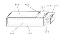
本発明に係る発光装置として面状発光光源の一例を図4に示す。
【0039】
図4に示す面状発光光源400では、色変換部材402である蛍光体含有シート状樹脂を導光板404状に配置させる。導光板は、光放出面となる主面及び光導入部となるLED光接合面を除いて反射部材405で覆われている。LEDチップ401、411を透光性樹脂412で被覆してある発光ダイオード403を光導入部に配置させてある。なお、発光ダイオードは導光板の端面に或いは底面に配置させることによっても面状発光光源とすることができる。
【0040】
LEDチップからの青色光は、導光板によって混色され略均一な色になった後、樹脂に含有された蛍光体によって部分的に黄色に変換されると共に変換されなかった光が青色光として取り出すことができる。蛍光体からの黄色光と、LEDチップからの青色光が面状に取り出すことができる。なお、色変換部材402を導光板404上に配置させたが、透光性部材412中に蛍光体を含有させLEDチップ401、411からの光及び蛍光体からの混色光を導光板404内に導入されることにより白色光として面状に取り出すこともできる。
【0041】
詳細に説明すると、図4の面状発光光源の断面において、半導体発光素子401、411は、絶縁層及び導電性パターン(図示せず)が形成されたコの字形状の樹脂パッケージ403内に固定される。発光素子の電極と導電性パターンとを導通させた後、蛍光体をエポキシ樹脂と混合して発光素子が積載されたコの字型の樹脂パッケージ内に充填等する。本発明では2個の半導体発光素子を配置させてある(図示せず)。こうして固定された発光素子は、アクリル性の導光板の一方の端面にエポキシ樹脂などで固定される。導光板の他方の主表面(裏面側)全面及びや発光素子が配置されていない他方の端面上にも反射部材を設け発光効率を向上させるように構成する。
【0042】
こうして例えば、LCDのバックライト用として十分な明るさを有する面状発光の発光装置を構成することができる。なお、ここでは、蛍光体含有樹脂を直接LEDチップ上に配置させたが、LEDチップをダイボンドさせるダイボンド樹脂中に蛍光体を含有させてもよいし、導光板404と発光ダイオードとの間に蛍光体含有樹脂をシート状にさせたフィルム(不示図)を配置させてもよい。以下、本願発明の具体的実施例について説明するが、本願発明はこれのみに限定されるものではないことは言うまでもない。
【0043】
【実施例】
(実施例1) 青色が発光可能なLEDチップとしてサファイヤ基板上にMOCVD法を用いて半導体発光素子を形成させる。半導体発光素子であるLEDチップはサファイア基板上に、低温で成膜させたGaN、ノンドープのn型GaN、コンタクト層となるSiドープされたn型GaN、ノンドープのn型GaN、GaNとInGaNを複数積層させた多重量子井戸構造となる発光層、クラッド層となるMgをドープさせたp型AlGaNとGaNの超格子層、コンタクト層となるMgをドープさせたp型GaNを形成させた後、エッチングにより各コンタクト層を露出後スパッタリング法にて電極を形成し、主として470nmの発光波長を有するLEDチップを形成させる。
【0044】
形成された半導体発光素子が発光スペクトルにおいて概ね正規分布をとる場合、主として最も数の多い発光スペクトルを境として第1の発光波長域と、第2の発光波長域に分けてある。具体的には発光波長分別機を用いて、発光波長域を461nmから470nmを第1の発光波長域と、471nmから480nmを第2の発光波長域として同色系の発光波長ごとに分類する。
【0045】
あらかじめ分別させた第1の発光波長域から第1のLEDチップ301を選択させてパッケージ305開口部の底面上にエポキシ樹脂によってダイボンドさせる。同様に、あらかじめ分別させた第2の発光波長域から第2のLEDチップ311を選択させてパッケージ305開口部の底面上にエポキシ樹脂によってダイボンドさせる。各LEDチップ301、311の電極とリード電極306、307、308とを金線303によってワイヤーボンディングさせた後、(Y・Gd)3Al5O12:Ce含有のエポキシ樹脂302をパッケージ305の凹部内に注入して硬化させる。こうして形成させた図3の如きSMD型発光ダイオード300となる発光装置は、一つのLEDチップを用いて同様に形成した発光装置と比較して一個当たりのLEDチップから放出される光密度が低く樹脂劣化にともなう輝度低下が極めて少ない。また、量産された発光装置間の色調及び輝度バラツキが極めて少なく色調による不良が激減し、歩留まりが大幅に向上することにより量産性に優れた発光装置とすることができる。
(実施例2)
実施例1で形成させたSMD型発光ダイオードの各LEDチップを個別に駆動できるようにリード電極をそれぞれ別々に金線にて接続させた以外は実施例1と同様にして形成させる。形成させたSMD型発光ダイオードの各LEDチップに流す振幅値となる電流値及び/又はパルス幅となる点灯時間の比をそれぞれ制御回路によって調整することによって複数のSMD型発光ダイオードの色調及び輝度バラツキをより少なく制御することができる。なお、このような投入電流などの制御を制御回路だけでなく、SMD型発光ダイオードに予め抵抗を設けるなどして調整することもできる。
【0046】
【発明の効果】
本願発明の請求項1の構成とすることにより、半導体発光素子の発光波長ズレに伴う色むらや輝度むらを補正しつつ歩留まりの高い表示装置を提供することができる。
【0047】
本願発明の請求項2の構成とすることにより、半導体発光素子の発光波長ズレに伴う色むらや輝度むらを補正しつつ歩留まりの高い表示装置の量産性よく製造することができる。
【図面の簡単な説明】
【図1】 本願発明に用いられる砲弾型発光ダイオードの模式的断面図である。
【図2】 本願発明に用いられる別の砲弾型発光ダイオードの模式的断面図である。
【図3】 本願発明に用いられるSMD型発光ダイオードの模式的断面図である。
【図4】 本願発明に用いられる面状光源の模式的断面図である。
【図5】 本願発明の原理を説明する模式的説明図である。
【符号の説明】
101…主発光波長が第1の発光波長域内である半導体発光素子群から選択された第1の半導体発光素子
102…色変換部材
103…金属ワイヤー
104…導電性ペースト
105…モールド部材
106…インナーリード
107…マウントリード
111…第1の発光波長域よりも主発光波長が長波長側にある第2の発光波長域内の半導体発光素子群から選択された第2の半導体発光素子
201…主発光波長が第1の発光波長域内である半導体発光素子群から選択された第1の半導体発光素子
202…色変換部材
203…導電性ワイヤー
204…導電性ペースト
205…モールド部材
206…マウントリード
207…インナーリード
208…インナーリード
211…第1の発光波長域よりも主発光波長が長波長側にある第2の発光波長域内の半導体発光素子群から選択された第2の半導体発光素子
213…導電性ワイヤー
300…SMD型発光ダイオード
301…主発光波長が第1の発光波長域内である半導体発光素子群から選択された第1の半導体発光素子
302…色変換部材
303…導電性ワイヤー
305…パッケージ
306…リード電極
307…リード電極
308…リード電極
311…第1の発光波長域よりも主発光波長が長波長側にある第2の発光波長域内の半導体発光素子群から選択された第2の半導体発光素子
401…主発光波長が第1の発光波長域内である半導体発光素子群から選択された第1の半導体発光素子
402…色変換部材
403…発光ダイオード
404…導光板
405…反射部材
407…LEDチップが点状に発光する蛍現象を抑制する反射部材
411…第1の発光波長域よりも主発光波長が長波長側にある第2の発光波長域内の半導体発光素子群から選択された第2の半導体発光素子
412…LEDチップを保護する透光性部材[0001]
[Industrial application fields]
The present invention relates to a light emitting device using a semiconductor light emitting element such as an LED (light emitting diode) or an LD (laser diode) and a phosphor, and particularly to provide a light emitting device with high luminance and little color variation.
[0002]
[Prior art]
Today, nitride semiconductors (typically, In x Ga y Al 1-xy N, 0 ≦ x ≦ 1, 0 ≦ y ≦ 1, 0 ≦ x + y ≦ 1), and a complementary color by absorbing blue light emitted from the LED chip and the LED chip. A light-emitting diode, which is a light-emitting device capable of emitting white light or the like by coating with a resin containing a phosphor capable of emitting yellow light or the like, has been developed.
[0003]
Such a light emitting diode can emit white light at two terminals of one chip. Compared to light bulbs and fluorescent lamps, it can be made smaller and generate less heat and can be made relatively simple. In particular, unlike a cold cathode tube, it does not require an inverter and is said to be environmentally friendly because it does not use Hg. In addition, because it has excellent characteristics such as low light consumption, such as a light bulb that is strong against vibration, it is rapidly being used in various fields such as liquid crystal backlights, various illuminations and indicators.
[0004]
[Problems to be solved by the invention]
However, higher brightness is required as the field of use expands, and the light emitting diode having the above configuration is not sufficient, and further output improvement is required. On the other hand, when a light emitting diode is provided on the end face of the light guide plate and applied to a liquid crystal backlight or the like, a plurality of light emitting diodes may be used because they are regarded as a macro point light source. In this case, the white color of the mixed color light is sensitive to human eyes as a color sensation and can be discriminated even with a slight color misalignment, so that a uniform color tone is particularly required.
[0005]
However, semiconductors used in light-emitting diodes are extremely difficult to form, and light emission characteristics vary due to slight differences in the raw material gas flow rate, substrate temperature, and impurity concentration. In order to form tens of thousands of LED chips from a semiconductor wafer of about 2 inches, it is practically difficult to use light emitting diodes that are selected and classified according to each product, for example, emission luminance. Even if only the light emitting diodes having the same characteristics are formed, the product has a very low yield.
[0006]
In particular, the characteristic variation of the phosphor used is extremely small compared to the characteristic variation of the semiconductor light emitting element, and the excitation spectrum of each phosphor formed is treated as a substantially constant value. The wavelength of the LED chip absorbed by the phosphor may vary greatly. For this reason, although the output discharge | released from LED chip is equivalent, the brightness | luminance emitted from the fluorescent substance of a light emitting diode will differ. In addition, since the emission spectrum of the semiconductor light emitting element is shifted depending on the current value and / or driving temperature, color deviation may occur depending on the current value and / or temperature as well if this characteristic is greatly different.
[0007]
Further, in the case of a light emitting diode using a light emission spectrum from an LED chip and a light mixture of light from a phosphor, the remaining light emission spectrum from the LED chip that is not absorbed by the phosphor is also used for color mixture light emission. Therefore, not only the color shift due to the luminance shift of the phosphor, but also the remaining emission spectrum component from the LED chip partially absorbed by the phosphor changes. For this reason, when the wavelength of the LED chip is shifted, the color tone and luminance of the emission spectrum emitted from the light emitting diode may be greatly changed more than the wavelength shift from the LED chip. Therefore, there is a problem that a light emitting diode having a target color tone cannot be formed and the yield is lowered.
[0008]
[Means for Solving the Problems]
In order to solve the above-described problems, the present invention has the following configuration.
A semiconductor light emitting device capable of emitting light of the same color system, wherein the main light emission wavelength is a plurality of light emission wavelength ranges obtained by classifying semiconductor light emitting devices of the same color system for each predetermined wavelength range. 461 nm or more and less than 468 nm Selected from the group of semiconductor light emitting elements within the first emission wavelength region The A first semiconductor light emitting device; Main emission wavelength is 475 nm or more and 482 nm or less Selected from the group of semiconductor light emitting elements within the second emission wavelength region The A second semiconductor light emitting element, wherein the first semiconductor light emitting element and the second semiconductor light emitting element are: It is a semiconductor light emitting device of the same color system in which light emission is absorbed by phosphors of the same composition and visible light having a longer wavelength than these light emission is emitted, The first semiconductor light emitting device Light emission And the second semiconductor light emitting device Both luminescence Absorbs these Emits visible light with longer wavelength than Above The phosphor-containing resin containing the phosphor is filled, and the upper surfaces and side surfaces of the first semiconductor light-emitting element and the second semiconductor light-emitting element are continuously covered with the phosphor-containing resin. A light-emitting device that emits mixed color light of one semiconductor light-emitting element, the second semiconductor light-emitting element, and the phosphor.
Semiconductor light-emitting elements of the same color system for each light emission wavelength range , A first emission wavelength range, a third emission wavelength range that is longer than the first emission wavelength range, and a second emission wavelength that is longer than the third emission wavelength range Area A process of classifying The main emission wavelength is A first semiconductor light emitting element selected from a group of semiconductor light emitting elements within a first emission wavelength range; The main emission wavelength is A step of selecting a second semiconductor light emitting element selected from a group of semiconductor light emitting elements within a second emission wavelength region; and the first semiconductor light emitting element and the second semiconductor light emitting element Is a semiconductor light emitting element of the same color system in which light emission is absorbed by phosphors of the same composition and visible light having a wavelength longer than these light emission is emitted, The first semiconductor light emitting device Light emission And the second semiconductor light emitting device Both luminescence Absorbs these Emits visible light with longer wavelength than Above Filling a phosphor-containing resin containing a phosphor and continuously covering the top surface and the side surface of the first semiconductor light-emitting element and the second semiconductor light-emitting element with the phosphor-containing resin. A method of manufacturing a light emitting device that emits mixed color light by the first semiconductor light emitting element, the second semiconductor light emitting element, and the phosphor.
Moreover, it has the following structures as another form of this invention.
Semiconductor light emitting devices capable of emitting visible light (101, 111, 201, 211, 301, 3111, 401, 411) and fluorescence that absorbs light emitted from the semiconductor light emitting device and emits visible light having a longer wavelength than this light emission A semiconductor light emitting device having at least two semiconductor light emitting elements (101, 111, 201, 211, 301, 311, 401, 411) capable of emitting at least the same color system, and semiconductor light emitting Each of the elements is a semiconductor light emitting element group in which a main light emission wavelength (also referred to as a main wavelength) is within a first light emission wavelength area among a plurality of light emission wavelength areas obtained by classifying semiconductor light emitting elements of the same color for each predetermined wavelength range. Selected from the selected first semiconductor light emitting element (101, 201, 301, 401) and the semiconductor light emitting element group in the second light emitting wavelength region whose main light emitting wavelength is longer than the first light emitting wavelength region Light emitting device using the second semiconductor light emitting element (111, 211, 311, 411) formed
[0009]
In this way, when compared with a light emitting device that emits light with a single chip light emitting element, in order to achieve the same output, when the output of light emitted from one semiconductor light emitting element is suppressed and light is emitted with a single chip Therefore, it is possible to reduce the light density and to suppress deterioration of the mold resin. Since the light-emitting device is formed by combining the selected semiconductor light-emitting elements, a very uniform light-emitting device with less luminance unevenness and color tone unevenness can be formed with high productivity.
[0010]
Also, the present invention Another form The method for manufacturing a light emitting device includes a semiconductor light emitting device capable of emitting visible light, and a phosphor that absorbs light emitted from the semiconductor light emitting device and emits visible light having a longer wavelength than the emitted light. It is. In particular, the step of classifying the semiconductor light emitting elements of the same color system into a plurality of light emitting wavelength ranges for each constant light emitting wavelength region range, and the grouped main light emitting wavelengths are selected from a group of semiconductor light emitting devices within the first light emitting wavelength region. A step of selecting the first semiconductor light emitting device, and a second semiconductor light emitting device selected from the semiconductor light emitting device group in the second light emitting wavelength region in which the main light emitting wavelength is longer than the first light emitting wavelength region. A step of selecting an element and at least the first semiconductor light emitting element and the second semiconductor light emitting element are used. As a result, it is possible to relatively easily form light emitting diodes having uniform light emission luminance and color tone with a high yield.
[0011]
DETAILED DESCRIPTION OF THE INVENTION
As a result of various experiments, the inventor of the present application uses two or more semiconductor light-emitting elements having a specific relationship in light-emitting diodes using phosphors, so that light emission without emission luminance, color tone unevenness, and luminance deterioration is not caused. The present inventors have found that the apparatus can be used and have come to make the present invention.
[0012]
That is, the characteristic variation of the phosphor is less than the characteristic variation of the semiconductor light emitting element. Therefore, fluctuations in the emission spectrum emitted from the phosphor are small compared to the semiconductor light emitting device. In the present invention, a plurality of LED chips of the same color system with many variations are classified for each fixed light emission wavelength, and LEDs selected from LED groups at both end regions are combined to emit mixed colors. As a result, it is possible to cancel manufacturing variations in the LED chips themselves and to form light emitting diodes having a relatively uniform main emission wavelength with a high yield.
[0013]
In particular, although there is little variation in the emission wavelength of the phosphor, the emission luminance from the phosphor may vary depending on the degree of overlap between the excitation spectrum of the phosphor and the emission spectrum of the light emitting element. For this reason, when using a color mixture of the light emitting element and the phosphor, there may be a case where the light emitting element is not merely varied. Therefore, when each semiconductor light emitting element is driven independently, the color tone can be corrected in more detail by independently controlling the light emission output and lighting time of each semiconductor light emitting element.
[0014]
As a specific example, a semiconductor light emitting device in which gallium nitride is formed on a SiC substrate and emitting blue light having a main emission wavelength in the range of 461 nm to 482 nm is used. The main emission wavelength of the LED chip is classified into three stages for each range of 7 nm. The first classification is set to the LED chip group A in which the main emission wavelength is in the emission wavelength region of 461 nm or more and less than 468 nm. The second classification is classified into LED chip group C whose main emission wavelength is in the emission wavelength range of 468 nm or more and less than 475 nm. The third classification is classified into the LED chip group B whose main emission wavelength is in the emission wavelength range of 475 nm or more and 482 nm or less. Such classification can be classified relatively easily by an emission wavelength classifier or the like. Normally, since the distribution of each formed LED chip is a normal distribution, if the place where the number of normal distributions is the largest is class C, the LED chip among the group of classified A, B, and C LED chips The LED chip selected from the group C is improved in mass productivity by forming a light emitting diode using two LED chips selected from the LED chip group C.
[0015]
That is, as shown in FIG. 2, the LED chip (201, 211) selected from the LED chip group C is die-bonded with Ag paste (204) or the like in the cup at the tip of the mount lead (206) constituting the lead electrode (206). . Two LED chips each selected from the LED chip group C are arranged in the cup of the mount lead. Wire bonding is performed by two inner leads (207, 208) facing the mount lead, the other electrode of each LED chip, and gold wires (203, 213), respectively. As shown in FIG. 1, the LED chips (101, 111) may be connected in parallel or have different pn polarities (for example, the substrate of one LED chip exhibits n-type conductivity and the other LED chip has The substrate exhibits p-type conductivity.) LED chips may be used in series connection. In FIG. 2, the two inner leads (207, 208) and the LED chip are electrically connected independently so that the LED chips (201, 2111) can be driven independently.
[0016]
Next, an epoxy resin (202) containing YAG: Ce or the like as a phosphor that absorbs blue light from the LED chip and emits complementary yellow fluorescence is electrically connected to each lead electrode. It arrange | positions on the connected LED chip. The epoxy resin may contain silicon oxide or the like in order to have a light diffusing action and thixotropy. A colorant may be included in order to adjust the color tone. In the phosphor, part of Y may be substituted with Gd, and part of Al may be substituted with In or Ga. Further, an activator such as Tb may be contained in addition to Ce. Furthermore, you may use the LED chip which fluorescent substance containing resin was previously formed by screen printing etc. on the surface.
[0017]
In this way, two LED chips capable of emitting blue light are coated with a phosphor-containing resin that converts the wavelength of blue light from the LED chip to a complementary yellow color, inside the casting case containing the epoxy resin. The cannonball type light emitting diode of the present invention in which the mold resin (205) is formed can be formed by taking out after being placed and cured.
[0018]
Also, instead of selecting two LED chips from only the LED chip group C to form a light emitting diode, one LED chip (201) from the LED chip group A and one LED from the LED chip group B are used. The bullet-type light emitting diode of the present invention is formed in the same manner as described above except that the chip (211) is selected and used together.
If it demonstrates using a typical chromaticity diagram in FIG. 5, the LED chip selected from LED chip group A will be represented by a square mark, and the LED chip selected from LED chip group B will be represented by a triangle mark. From the light emitting diode, the light emitted from these LED chips corresponds to the black circle mark of the LED chip group C in a pseudo manner, and is represented on the two-dotted line between the black circle and the X mark which is the light emitted from the phosphor. Light can be expressed. Note that the color between the LED chip and the phosphor can be adjusted in accordance with the amount of the phosphor and the like, and can be brought into an ellipse of a one-dot chain line in the figure representing a pseudo white region.
[0019]
In any light emitting diode, variations in color tone and luminance variations emitted from the light emitting diode are reduced in each stage as compared with light emitting diodes formed without classification. In addition, although the luminance is increased, the light emitting diode can be obtained in which the luminance is less decreased due to resin deterioration.
[0020]
Next, by controlling the ratio of the current passed through each LED chip, the color mixture that is more electrically adjusted according to the ratio of the emission wavelength and luminance of the LED chip and the emission spectrum from the phosphor by controlling the ratio of the current passed through each LED chip. Light can be emitted. Hereafter, the structure used for this invention is explained in full detail.
(Emission wavelength range)
The emission wavelength range used in the present invention refers to a group of LEDs that emit similar emission wavelengths of the same color system classified into desired emission wavelength ranges. For example, a general chromaticity classification of system color names (JIS) Z8110) is a group in which the main emission wavelength of the blue region in the same color system is classified into a plurality of emission wavelength ranges. The classifications do not have to overlap each other, and may partially overlap for higher accuracy. In some cases, the same color system may refer to an area including blue-violet, blue, and blue-green areas. Therefore, various emission wavelength regions can be selected depending on the desired light emitting device. Specifically, the light emission wavelength region may be 460 nm to 475 nm as the first light emission wavelength region, and 475 nm to 490 nm as the second light emission wavelength region.
[0021]
In these classifications, the emission wavelength region may be narrowed or widened as desired. That is, the emission wavelength range can be variously selected depending on the use of the light emitting device used. Further, the semiconductor light emitting element group is not limited to three classifications, and may be two classifications or five classifications or more. In that case, in order to emit a desired wavelength from the LED, the desired wavelength range can be made closer by using a color mixture of the semiconductor light emitting element groups symmetrical about the desired wavelength range.
[0022]
It is preferable to classify the semiconductor light emitting elements for each of a plurality of light emitting wavelength ranges so that the formed semiconductor light emitting elements are within a desired light emitting wavelength range. As for the classified semiconductor light emitting elements, the semiconductor light emitting elements are selected from the respective light emission wavelength regions around the desired light emission wavelength region so as to be within the desired light emission wavelength region due to color mixing. The resulting light-emitting device has a semiconductor light-emitting element having a main emission wavelength longer than the average emission wavelength of the semiconductor light-emitting element displayed in a mixed color and a main light emission shorter than the average emission wavelength displayed in a mixed-color display. A semiconductor light emitting device having a wavelength is used. Thus, sorting the semiconductor light emitting elements for each emission wavelength region can be performed relatively easily using an automatic sorter.
[0023]
In the present invention, only the main emission wavelength has been described, but depending on the case, it is not only the classification of the emission wavelength region. The formed semiconductor light emitting element has a distribution in various characteristics such as Vf and temperature characteristics. By classifying such distributions, selecting and extracting from the classified ones, and combining them again, a semiconductor light emitting device having stable characteristics can be obtained. That is, a semiconductor light emitting device such as an LD or LED has at least two semiconductor light emitting devices capable of emitting at least the same color system, and each of the semiconductor light emitting devices has a constant driving voltage and / or driving current range. A first semiconductor light emitting element selected from a group of semiconductor light emitting elements having a driving voltage and / or a driving current in the first area among the plurality of areas classified for each of the areas; A second semiconductor light emitting element selected from the semiconductor light emitting element group in the second region where the drive voltage and / or drive current is high or low may be used.
[0024]
The visible light of the present invention preferably has a main emission wavelength of about 380 nm to about 680 nm. The visible light emitted from the semiconductor light emitting device preferably used in the present invention is about 380 nm to 530 nm, and more preferably 400 nm to 500 nm. More preferable visible light emitted from the semiconductor light emitting device is 410 nm to 490 nm.
(Semiconductor light emitting
Examples of the semiconductor light emitting device used in the present invention include LED chips and LDs using various semiconductors. Specific semiconductor light emitting devices include sapphire, spinel, SiC, and the like by liquid phase growth, metal organic chemical vapor deposition (MOCVD), halide vapor deposition (HDVPE), molecular beam vapor deposition (MBE), and the like. A light emitting element in which a semiconductor such as GaAlN, ZnS, ZnSe, SiC, GaP, GaAlAs, AlInGaP, InGaN, GaN, and AlInGaN is formed as a light emitting layer on a substrate made of GaN or the like is preferably used. Examples of the semiconductor structure include a homo structure having a MIS junction, a PIN junction, and a pn junction, a hetero structure, and a double hetero structure. Various emission wavelengths can be selected depending on the material of the semiconductor layer and the degree of mixed crystal.
[0025]
Furthermore, in order to have a quantum effect, a single quantum well structure or a multiple quantum well in which a well layer and a barrier layer having a band gap larger than that of a well layer are formed as well + barrier +... + Barrier + well or vice versa. It is good also as a structure. Particularly in a multiple quantum well structure in a nitride-based compound semiconductor, it is preferable that the well layer has a thickness of 70 angstroms or less and the barrier layer has a thickness of 150 angstroms or less. On the other hand, in the single quantum well structure, the thickness is preferably adjusted to 70 angstroms or less. Thus, a light emitting element with high light emission output can be obtained. In the semiconductor wafer on which each semiconductor layer is formed, each conductive type semiconductor layer is exposed by etching or the like, and then each electrode is formed by sputtering or vacuum deposition. An LED chip can be formed by cutting a semiconductor wafer on which electrodes are formed as desired.
[0026]
In addition, since the phosphor can emit light efficiently because the emission spectrum has a longer wavelength than the absorption spectrum, it is preferable that the visible light emitted from the semiconductor light emitting element has a shorter wavelength than the phosphor. . For this reason, nitride semiconductors (In x Ga y Al 1-xy N, where 0 ≦ x ≦ 1, 0 ≦ y ≦ 1). In order to configure the light emitting device of the present invention with a relatively simple configuration, it is preferable to have a light emitting layer made of a nitride semiconductor containing In. Therefore, as a specific configuration of the semiconductor light emitting device used in the present invention, a contact layer which is a gallium nitride semiconductor having n-type conductivity on a sapphire substrate, a cladding layer which is a gallium aluminum nitride semiconductor having p-type conductivity, p Of non-doped InGaN having a single quantum well structure between a contact layer having n-type conductivity and a clad layer having p-type conductivity, having a contact layer that is a gallium nitride semiconductor having type conductivity And a light-emitting element having a layer (a gallium nitride semiconductor is formed on a sapphire substrate at a low temperature and a buffer layer is provided).
[0027]
When an LED chip or the like having such a semiconductor light emitting layer is coated with a mold resin or the like, it is die-bonded with an epoxy resin or the like in a cup of a mount lead that becomes one electrode. Next, each electrode of the LED chip is electrically connected to the mount lead and the inner lead by a conductive wire such as a conductive wire such as gold or aluminum wire or a resin containing silver or ITO. After taking electrical continuity, the LED chip is covered with phosphor-containing resin or glass. Thereafter, the light emitting device can be formed by covering with a mold member in a desired shape with an epoxy resin, low melting point glass, or the like. In the present invention, in particular, two or more LED chips are arranged and each LED chip has a specific relationship. Note that the LED chip may be fixed on the substrate with a conductive paste or the like, and after being electrically connected, it may be covered with a mold member to form a light emitting device.
[0028]
In the present invention, it is possible to reduce the light emission luminance per unit by using two or more light emission luminances which are normally obtained with one light emitting element. This can be done by reducing the size of the LED chip itself or shortening the current flowing through the LED chip and the driving time. As a result, when a layer structure such as a double hetero structure is adopted for high output, the problem that the resin near the LED chip, such as the end face of the LED chip, deteriorates rapidly as the output from the LED chip improves. It can be solved easily. Similarly, a light-emitting device capable of emitting higher luminance while suppressing deterioration can be obtained.
(
Examples of the color conversion member used in the light emitting device of the present invention include phosphors (including organic and inorganic fluorescent dyes and fluorescent pigments), and those obtained by fixing these phosphors in a resin or glass. The phosphor is a phosphor that emits light when excited by visible light emitted from a semiconductor light emitting device. As a specific photoluminescent phosphor, it is an example of an yttrium-aluminum-garnet phosphor activated with cerium (RE). 1-x Sm x ) Three Al Five O 12 : Ce photoluminescent phosphor (where 0 ≦ x <1, RE is at least one selected from Y, Gd, and La. Note that a part of Al may be substituted with Ga or In. Further, an activator such as Tb may be separately added in addition to Ce.), Nitrogen-containing CaO—Al activated by perylene derivatives, copper and aluminum activated zinc sulfide and Eu and / or Cr 2 O Three -SiO 2 A phosphor is preferably used.
[0029]
In such a phosphor, an oxide or a compound that easily becomes an oxide at a high temperature is used as a raw material for Y, Ce, and Al, and these are sufficiently mixed in a stoichiometric ratio to obtain a raw material. Alternatively, a mixture of a coprecipitated oxide obtained by calcining a solution obtained by coprecipitation of oxalic acid with a solution obtained by dissolving a rare earth element of Y or Ce in an acid in a stoichiometric ratio, and aluminum oxide or gallium oxide is mixed. Get raw materials. An appropriate amount of fluoride such as ammonium fluoride is mixed with this as a flux and packed in a crucible, fired in air at a temperature range of 1350 to 1450 ° C. for 2 to 5 hours to obtain a fired product, and then the fired product in water. It can be obtained by ball milling, washing, separating, drying and finally passing through a sieve.
[0030]
Similarly, nitrogen-containing CaO—Al activated by Eu and / or Cr, which are other specific phosphors used in the present invention. 2 O Three -SiO 2 Phosphors are melted at 1300 ° C. to 1900 ° C. (more preferably 1500 ° C. to 1750 ° C.) in a nitrogen atmosphere by mixing a raw material such as aluminum oxide, yttrium oxide, silicon nitride and calcium oxide in a predetermined ratio with a rare earth material. Then mold. The molded product can be ball milled, washed, separated, dried, and finally passed through a sieve to form a phosphor. As a result, Ca—Al—Si—O—N-based oxynitride fluorescence activated by Eu and / or Cr that can emit red light by an excitation spectrum having a peak at 450 nm and blue light having a peak at about 650 nm. Can be glass.
[0031]
The peak of the emission spectrum is continuously shifted from 575 nm to 690 nm by increasing or decreasing the nitrogen content of the Ca—Al—Si—O—N-based oxynitride fluorescent glass activated with Eu and / or Cr. be able to. Similarly, the excitation spectrum can be shifted continuously. Therefore, white light can be emitted by the combined light of the light from the semiconductor light emitting element selected according to the present invention and the light of the phosphor of about 580 nm.
[0032]
Further, according to the present invention, the above-described YAG phosphor activated with Ce and the nitrogen-containing Ca—Al—Si—ON—oxynitride fluorescent glass activated with Eu and / or Cr are combined. A light-emitting diode capable of emitting white light with extremely high color rendering properties including RGB (red, green, blue) components with high luminance can be formed using a selected semiconductor light-emitting element capable of emitting blue light. For this reason, an arbitrary intermediate color can be formed very simply by adding a desired pigment.
(Mold members 105 and 205)
The mold members 105 and 205 are preferably provided to protect the
[0033]
The colorant is used for providing a filter effect that improves light emission characteristics by cutting undesired wavelengths in the light emitted from the LED chip contained in the mold member. Therefore, various dyes and pigments are selected according to the emission color of the LED or phosphor, or in order to obtain an intermediate color such as pink or light blue which is a desired color to be taken out from the light emitting device. Further, the colorant may be formed by being dispersed in various proportions in the mold member as desired. That is, the concentration can be increased or decreased as the LED chip is approached.
[0034]
Further, a phosphor that converts light from the LED chip may be contained in the mold member. Mixing colorants, diffusing agents, and phosphors into mold members can be done by mixing and stirring colorants in the mold material, and then using LED chips etc. that can be formed into the desired mold member shape such as a shell shape. It can be formed by putting together with heat curing.
[0035]
Including white by adjusting the ratio and coating of phosphor and resin, the average particle size and center particle size of phosphor, particle size distribution, various composition ratios, filling amount and selecting the emission wavelength of light emitting element Arbitrary colors such as a light bulb color can be provided. The distribution of the photoluminescence phosphor can be variously formed by adjusting the member containing the photoluminescence phosphor, the forming temperature, the viscosity, the shape of the photoluminescence phosphor, the particle size distribution, and the like. Accordingly, various distribution concentrations of the phosphor can be selected depending on the use conditions and the like.
(Lead
The lead electrode is for supplying electric power to each semiconductor light emitting element, and an LED chip or the like, which is a semiconductor light emitting element, may be die-bonded thereon or may only have a function of being electrically connected. When the LED chip is disposed on the lead electrode, a recess may be formed by using a part of the lead electrode in order to effectively use light, and the LED chip may be disposed inside.
[0036]
The LED chip having a cup or the like in which the LED chip is disposed on the lead electrode is used as a mount lead. The size of the cup is large enough to load each LED chip with a device such as a die bond, and various types of cups are used according to the light condensing rate of the mold member. In the present invention, three or more LED chips for color mixture correction may be arranged in the cup. Accordingly, the LED chip can use, for example, two light emitting elements which emit light of different wavelengths selected by the present invention in the same color system and one light emitting element capable of emitting red light. Thereby, it can also be set as the light-emitting device which can light-emit red and white and pink. The cup may be directly electrically connected to the LED chip and used as an electrode. Further, the LED chip may be fixed to the cup via an insulator so as to be non-conductive. When the mount lead is used as an electrode of each LED chip, sufficient electrical conductivity and connectivity with a bonding wire or the like are required.
[0037]
Each LED chip and the cup can be connected by a thermosetting resin or the like. Specifically, an epoxy resin, an acrylic resin, an imide resin, etc. are mentioned. Further, in order to adhere and electrically connect the LED chip and the cup, a conductive paste or a metal bump containing a conductive member such as Ag, Cu, carbon, or ITO can be used.
[0038]
As the other electrode constituting the pair of lead electrodes of the mount lead, there is an inner lead. The inner lead is required to have connectivity and electrical conductivity with a bonding wire or the like that is an electrical connection member. Preferred examples of such a lead electrode material include iron, copper, iron-containing copper, tin-containing copper, and the like.
(
The conductive wire is required to have good ohmic properties, mechanical connectivity, electrical conductivity and thermal conductivity with the electrodes of each LED chip. The thermal conductivity is preferably 0.01 cal /
An example of a planar light source as a light emitting device according to the present invention is shown in FIG.
[0039]
In the planar light source 400 shown in FIG. 4, the phosphor-containing sheet-like resin that is the color conversion member 402 is arranged in the shape of the light guide plate 404. The light guide plate is covered with a reflecting member 405 except for the main surface serving as a light emitting surface and the LED light joining surface serving as a light introducing portion. A light-emitting diode 403 in which the LED chips 401 and 411 are covered with a translucent resin 412 is arranged in the light introducing portion. The light emitting diode can also be used as a planar light source by being disposed on the end face or the bottom face of the light guide plate.
[0040]
After the blue light from the LED chip is mixed by the light guide plate to become a substantially uniform color, it is partially converted to yellow by the phosphor contained in the resin and the unconverted light is taken out as blue light. Can do. Yellow light from the phosphor and blue light from the LED chip can be extracted in a planar shape. Although the color conversion member 402 is disposed on the light guide plate 404, the light-transmitting member 412 contains a fluorescent material so that the light from the LED chips 401 and 411 and the mixed color light from the fluorescent material are contained in the light guide plate 404. By being introduced, it can be taken out in the form of white light.
[0041]
More specifically, in the cross section of the planar light source shown in FIG. 4, the semiconductor light emitting elements 401 and 411 are fixed in a U-shaped resin package 403 in which an insulating layer and a conductive pattern (not shown) are formed. Is done. After the electrode of the light emitting element and the conductive pattern are made conductive, the phosphor is mixed with an epoxy resin and filled into a U-shaped resin package on which the light emitting element is loaded. In the present invention, two semiconductor light emitting elements are arranged (not shown). The light emitting element thus fixed is fixed to one end face of the acrylic light guide plate with an epoxy resin or the like. A reflection member is also provided on the entire other main surface (back surface side) of the light guide plate and on the other end surface where the light emitting element is not disposed, so that the light emission efficiency is improved.
[0042]
Thus, for example, a planar light emitting device having sufficient brightness for an LCD backlight can be configured. Here, the phosphor-containing resin is directly disposed on the LED chip. However, the phosphor may be contained in a die-bonding resin for die-bonding the LED chip, or the fluorescent material may be interposed between the light guide plate 404 and the light-emitting diode. You may arrange | position the film (not shown) which made the body containing resin the sheet form. Hereinafter, specific examples of the present invention will be described, but it goes without saying that the present invention is not limited thereto.
[0043]
【Example】
Example 1 A semiconductor light emitting element is formed on a sapphire substrate as an LED chip capable of emitting blue light by using the MOCVD method. The LED chip which is a semiconductor light emitting device has a plurality of GaN formed on a sapphire substrate, non-doped n-type GaN, Si-doped n-type GaN serving as a contact layer, non-doped n-type GaN, GaN and InGaN. Etching after forming a stacked light emitting layer having a multiple quantum well structure, a p-type AlGaN and GaN superlattice layer doped with Mg as a cladding layer, and a p-type GaN doped with Mg as a contact layer After exposing each contact layer, an electrode is formed by sputtering to form an LED chip mainly having an emission wavelength of 470 nm.
[0044]
When the formed semiconductor light emitting element has a substantially normal distribution in the emission spectrum, it is divided into a first emission wavelength region and a second emission wavelength region mainly with the largest emission spectrum as a boundary. Specifically, using a light emission wavelength classifier, the light emission wavelength region is classified for each light emission wavelength of the same color system, with 461 nm to 470 nm as the first light emission wavelength region and 471 nm to 480 nm as the second light emission wavelength region.
[0045]
The first LED chip 301 is selected from the first emission wavelength range that has been separated in advance, and die-bonded to the bottom surface of the opening of the package 305 with an epoxy resin. Similarly, the second LED chip 311 is selected from the second emission wavelength region that has been separated in advance, and die-bonded to the bottom surface of the package 305 with an epoxy resin. After the electrodes of the LED chips 301 and 311 and the
(Example 2)
It is formed in the same manner as in Example 1 except that the lead electrodes are individually connected by gold wires so that each LED chip of the SMD type light emitting diode formed in Example 1 can be individually driven. The color value and brightness variation of the plurality of SMD type light emitting diodes are adjusted by adjusting the ratio of the current value as the amplitude value and / or the lighting time as the pulse width flowing through each LED chip of the formed SMD type light emitting diode by the control circuit, respectively. Can be controlled less. It should be noted that such control of the input current can be adjusted not only by the control circuit but also by providing a resistor in advance in the SMD type light emitting diode.
[0046]
【Effect of the invention】
With the configuration of the first aspect of the present invention, it is possible to provide a display device with a high yield while correcting color unevenness and luminance unevenness due to emission wavelength shift of the semiconductor light emitting element.
[0047]
By adopting the configuration of
[Brief description of the drawings]
FIG. 1 is a schematic cross-sectional view of a bullet-type light emitting diode used in the present invention.
FIG. 2 is a schematic cross-sectional view of another bullet-type light emitting diode used in the present invention.
FIG. 3 is a schematic cross-sectional view of an SMD type light emitting diode used in the present invention.
FIG. 4 is a schematic cross-sectional view of a planar light source used in the present invention.
FIG. 5 is a schematic explanatory view illustrating the principle of the present invention.
[Explanation of symbols]
101... First semiconductor light emitting element selected from the group of semiconductor light emitting elements whose main emission wavelength is within the first emission wavelength range
102: Color conversion member
103 ... Metal wire
104 ... conductive paste
105 ... Mold member
106 ... Inner lead
107 ... Mount lead
111... A second semiconductor light emitting element selected from the group of semiconductor light emitting elements in the second light emission wavelength region in which the main light emission wavelength is longer than the first light emission wavelength region
201: a first semiconductor light emitting element selected from the group of semiconductor light emitting elements whose main emission wavelength is in the first emission wavelength range
202 ... color conversion member
203 ... Conductive wire
204 ... conductive paste
205 ... Mold member
206 ... Mount lead
207 ... Inner lead
208 ... Inner lead
211... A second semiconductor light emitting element selected from the group of semiconductor light emitting elements in the second light emission wavelength region in which the main light emission wavelength is longer than the first light emission wavelength region
213 ... Conductive wire
300 ... SMD type light emitting diode
301. First semiconductor light emitting element selected from the group of semiconductor light emitting elements whose main emission wavelength is within the first emission wavelength range
302 ... Color conversion member
303 ... Conductive wire
305 ... Package
306 ... Lead electrode
307 ... Lead electrode
308 ... Lead electrode
311... Second semiconductor light emitting element selected from the group of semiconductor light emitting elements in the second light emission wavelength region in which the main light emission wavelength is longer than the first light emission wavelength region
401... A first semiconductor light emitting element selected from the group of semiconductor light emitting elements whose main emission wavelength is within the first emission wavelength range
402: Color conversion member
403 ... Light emitting diode
404 ... light guide plate
405: Reflecting member
407 ... Reflective member that suppresses the firefly phenomenon in which the LED chip emits light in the form of dots
411... A second semiconductor light emitting element selected from the group of semiconductor light emitting elements in the second light emission wavelength region in which the main light emission wavelength is longer than the first light emission wavelength region
412 ... Translucent member for protecting the LED chip
Claims (2)
前記第1の半導体発光素子及び前記第2の半導体発光素子は、同一組成の蛍光体によって発光が吸収されこれらの発光よりも長波長の可視光が発光される同色系の半導体発光素子であり、前記第1の半導体発光素子の発光及び前記第2の半導体発光素子の発光の両方を吸収しこれらの発光よりも長波長の可視光を発光する前記蛍光体が含有された蛍光体含有樹脂が充填されて前記第1の半導体発光素子及び前記第2の半導体発光素子の上面及び側面が連続して前記蛍光体含有樹脂に覆われており、前記第1の半導体発光素子と、前記第2の半導体発光素子と、前記蛍光体と、による混色光を発光することを特徴とする発光装置。1st light emission which is a semiconductor light emitting element which can emit light of the same color system, and the main light emission wavelength is 461 nm or more and less than 468 nm among a plurality of light emission wavelength ranges in which the semiconductor light emitting elements of the same color system are classified for each fixed wavelength range. the first semiconductor light emitting element and the second semiconductor light-emitting device main emission wavelength is selected from a second emission wavelength region of the semiconductor light emitting element groups below 482nm or 475nm selected from the semiconductor light emitting element group which is the wavelength region And having
The first semiconductor light emitting element and the second semiconductor light emitting element are semiconductor light emitting elements of the same color system in which light emission is absorbed by phosphors of the same composition and visible light having a longer wavelength than these light emission is emitted. emission and the second semiconductor light emitting element phosphor-containing resin in which the phosphor is contained to absorb both light emission than the light-emitting emits visible light of a long wavelength of filling of the first semiconductor light emitting element The upper surface and the side surface of the first semiconductor light emitting device and the second semiconductor light emitting device are continuously covered with the phosphor-containing resin, and the first semiconductor light emitting device and the second semiconductor A light-emitting device that emits mixed color light from a light-emitting element and the phosphor.
主発光波長が前記第1の発光波長域内である半導体発光素子群から選択された第1の半導体発光素子と、主発光波長が前記第2の発光波長域内の半導体発光素子群から選択された第2の半導体発光素子と、を選択する工程と、
前記第1の半導体発光素子及び前記第2の半導体発光素子は、同一組成の蛍光体によって発光が吸収されこれらの発光よりも長波長の可視光が発光される同色系の半導体発光素子であり、前記第1の半導体発光素子の発光及び前記第2の半導体発光素子の発光の両方を吸収しこれらの発光よりも長波長の可視光を発光する前記蛍光体が含有された蛍光体含有樹脂を充填して前記第1の半導体発光素子及び前記第2の半導体発光素子の上面及び側面を連続して前記蛍光体含有樹脂で覆う工程と、を有し、前記第1の半導体発光素子と、前記第2の半導体発光素子と、前記蛍光体と、による混色光を発光する発光装置の製造方法。The semiconductor light emitting element of the same color system is divided into a first emission wavelength range, a third emission wavelength range that is longer than the first emission wavelength range, and a third emission wavelength range for each constant emission wavelength range . Classifying into a second emission wavelength range that is longer than the emission wavelength range ;
The main emission wavelength is selected from the first of the first semiconductor light emitting element and a main emission wavelength and the second emission wavelength range of the semiconductor light emitting element group selected from the semiconductor light emitting element group which is the emission wavelength region A step of selecting a semiconductor light-emitting element of 2;
The first semiconductor light emitting element and the second semiconductor light emitting element are semiconductor light emitting elements of the same color system in which light emission is absorbed by phosphors of the same composition and visible light having a longer wavelength than these light emission is emitted. filling the phosphor-containing resin in which the phosphor is contained to emit visible light of the first absorbing both light emission of emission and the second semiconductor light emitting element of the semiconductor light emitting element longer wavelength than the light-emitting And continuously covering the top surface and the side surface of the first semiconductor light emitting element and the second semiconductor light emitting element with the phosphor-containing resin, and the first semiconductor light emitting element, A method of manufacturing a light emitting device that emits mixed color light by the semiconductor light emitting element of 2 and the phosphor.
Priority Applications (1)
| Application Number | Priority Date | Filing Date | Title |
|---|---|---|---|
| JP2000368603A JP4932078B2 (en) | 2000-12-04 | 2000-12-04 | Light emitting device and manufacturing method thereof |
Applications Claiming Priority (1)
| Application Number | Priority Date | Filing Date | Title |
|---|---|---|---|
| JP2000368603A JP4932078B2 (en) | 2000-12-04 | 2000-12-04 | Light emitting device and manufacturing method thereof |
Related Child Applications (1)
| Application Number | Title | Priority Date | Filing Date |
|---|---|---|---|
| JP2011008820A Division JP5606342B2 (en) | 2011-01-19 | 2011-01-19 | Light emitting device |
Publications (2)
| Publication Number | Publication Date |
|---|---|
| JP2002170999A JP2002170999A (en) | 2002-06-14 |
| JP4932078B2 true JP4932078B2 (en) | 2012-05-16 |
Family
ID=18838804
Family Applications (1)
| Application Number | Title | Priority Date | Filing Date |
|---|---|---|---|
| JP2000368603A Expired - Lifetime JP4932078B2 (en) | 2000-12-04 | 2000-12-04 | Light emitting device and manufacturing method thereof |
Country Status (1)
| Country | Link |
|---|---|
| JP (1) | JP4932078B2 (en) |
Families Citing this family (25)
| Publication number | Priority date | Publication date | Assignee | Title |
|---|---|---|---|---|
| EP1662583B1 (en) * | 2003-07-28 | 2018-11-07 | Nichia Corporation | Light-emitting apparatus, led illumination, led light-emitting apparatus, and method of controlling light-emitting apparatus |
| US7737623B2 (en) * | 2004-06-30 | 2010-06-15 | Mitsubishi Chemical Corporation | Light emitting device, lighting system, backlight unit for display device, and display device |
| JP4534717B2 (en) * | 2004-10-29 | 2010-09-01 | 豊田合成株式会社 | Light emitting device |
| KR101142961B1 (en) * | 2005-03-29 | 2012-05-08 | 서울반도체 주식회사 | Led lamp mounting a led having an array of light emitting cells coupled in series |
| EP1864339A4 (en) | 2005-03-11 | 2010-12-29 | Seoul Semiconductor Co Ltd | Led package having an array of light emitting cells coupled in series |
| JP2006295084A (en) * | 2005-04-14 | 2006-10-26 | Citizen Electronics Co Ltd | Package structure of light emitting diode |
| KR101171186B1 (en) * | 2005-11-10 | 2012-08-06 | 삼성전자주식회사 | High luminance light emitting diode and liquid crystal display panel of using the same |
| JP5027427B2 (en) * | 2006-02-23 | 2012-09-19 | パナソニック株式会社 | White illumination device using light emitting diode |
| EP2052589A4 (en) * | 2006-04-18 | 2012-09-19 | Cree Inc | Lighting device and lighting method |
| KR101258227B1 (en) | 2006-08-29 | 2013-04-25 | 서울반도체 주식회사 | Light emitting device |
| US7902560B2 (en) * | 2006-12-15 | 2011-03-08 | Koninklijke Philips Electronics N.V. | Tunable white point light source using a wavelength converting element |
| JP5106862B2 (en) * | 2007-01-15 | 2012-12-26 | 昭和電工株式会社 | Light emitting diode package |
| JP5040355B2 (en) * | 2007-02-24 | 2012-10-03 | 日亜化学工業株式会社 | Semiconductor light emitting device and light emitting device having the same |
| KR101081246B1 (en) * | 2008-11-21 | 2011-11-08 | 엘지이노텍 주식회사 | Light emitting apparatus and fabrication method thereof |
| KR100999809B1 (en) * | 2010-03-26 | 2010-12-08 | 엘지이노텍 주식회사 | Light emitting device and light unit having thereof |
| WO2012042962A1 (en) | 2010-09-30 | 2012-04-05 | 日亜化学工業株式会社 | Light-emitting apparatus and method of manufacturing light-emitting apparatus |
| KR101725220B1 (en) | 2010-12-22 | 2017-04-10 | 삼성전자 주식회사 | Method of depositing phosphor on semiconductor light emitting device and an apparatus for depositing phosphor on semiconductor light emitting device |
| JP2012227397A (en) * | 2011-04-20 | 2012-11-15 | Sharp Corp | Light source manufacturing method and light source |
| JP5390566B2 (en) * | 2011-07-14 | 2014-01-15 | シャープ株式会社 | LIGHT EMITTING DEVICE PRODUCTION DEVICE AND ITS PRODUCTION METHOD, LIGHT EMITTING MODULE PRODUCTION DEVICE AND ITS PRODUCTION METHOD, LIGHT EMITTING MODULE, LIGHT SOURCE DEVICE, AND LIQUID CRYSTAL DISPLAY DEVICE |
| JP5341154B2 (en) * | 2011-08-31 | 2013-11-13 | 株式会社フジクラ | High color rendering LED lamp unit |
| JP2013135083A (en) | 2011-12-26 | 2013-07-08 | Toyoda Gosei Co Ltd | Light-emitting device |
| JP2013135082A (en) | 2011-12-26 | 2013-07-08 | Toyoda Gosei Co Ltd | Light-emitting device |
| JP2014007355A (en) * | 2012-06-27 | 2014-01-16 | Rohm Co Ltd | Semiconductor light-emitting device and lighting device |
| JP2014096505A (en) * | 2012-11-09 | 2014-05-22 | Sharp Corp | Backlight and method for manufacturing the same |
| JP2015012119A (en) * | 2013-06-28 | 2015-01-19 | 京セラ株式会社 | Light irradiation device, light irradiation module and printer |
Family Cites Families (5)
| Publication number | Priority date | Publication date | Assignee | Title |
|---|---|---|---|---|
| JPH07297449A (en) * | 1994-04-27 | 1995-11-10 | Rohm Co Ltd | Led lamp of its manufacture |
| JP3219000B2 (en) * | 1996-12-27 | 2001-10-15 | 日亜化学工業株式会社 | LED display and manufacturing method thereof |
| EP1959506A2 (en) * | 1997-01-31 | 2008-08-20 | Matsushita Electric Industrial Co., Ltd. | Method of manufacturing a semiconductor light-emitting device |
| JP4109756B2 (en) * | 1998-07-07 | 2008-07-02 | スタンレー電気株式会社 | Light emitting diode |
| JP4207252B2 (en) * | 1998-07-27 | 2009-01-14 | ソニー株式会社 | Display device |
-
2000
- 2000-12-04 JP JP2000368603A patent/JP4932078B2/en not_active Expired - Lifetime
Also Published As
| Publication number | Publication date |
|---|---|
| JP2002170999A (en) | 2002-06-14 |
Similar Documents
| Publication | Publication Date | Title |
|---|---|---|
| JP4932078B2 (en) | Light emitting device and manufacturing method thereof | |
| JP6101943B2 (en) | Light emitting device and display device | |
| JP4101468B2 (en) | Method for manufacturing light emitting device | |
| JP2927279B2 (en) | Light emitting diode | |
| JP3065258B2 (en) | Light emitting device and display device using the same | |
| JP3655267B2 (en) | Semiconductor light emitting device | |
| JP2010103522A (en) | Ac drive type light-emitting element with delay phosphor and light-emitting element module | |
| JPH10247750A (en) | Led lamp | |
| JP5606342B2 (en) | Light emitting device | |
| JP3367096B2 (en) | Method of forming light emitting diode | |
| JP3604298B2 (en) | Method of forming light emitting diode | |
| US7999274B2 (en) | White light emitting device | |
| JP3858829B2 (en) | Method for forming light emitting diode | |
| JPH11243232A (en) | Led display device | |
| JP2003008082A (en) | Light emitting diode and method for forming the same | |
| JP3674387B2 (en) | Light emitting diode and method for forming the same |
Legal Events
| Date | Code | Title | Description |
|---|---|---|---|
| A621 | Written request for application examination |
Free format text: JAPANESE INTERMEDIATE CODE: A621 Effective date: 20071017 |
|
| A977 | Report on retrieval |
Free format text: JAPANESE INTERMEDIATE CODE: A971007 Effective date: 20100520 |
|
| A131 | Notification of reasons for refusal |
Free format text: JAPANESE INTERMEDIATE CODE: A131 Effective date: 20100601 |
|
| A521 | Request for written amendment filed |
Free format text: JAPANESE INTERMEDIATE CODE: A523 Effective date: 20100802 |
|
| A02 | Decision of refusal |
Free format text: JAPANESE INTERMEDIATE CODE: A02 Effective date: 20101019 |
|
| A521 | Request for written amendment filed |
Free format text: JAPANESE INTERMEDIATE CODE: A523 Effective date: 20110119 |
|
| A911 | Transfer to examiner for re-examination before appeal (zenchi) |
Free format text: JAPANESE INTERMEDIATE CODE: A911 Effective date: 20110127 |
|
| A912 | Re-examination (zenchi) completed and case transferred to appeal board |
Free format text: JAPANESE INTERMEDIATE CODE: A912 Effective date: 20110225 |
|
| A521 | Request for written amendment filed |
Free format text: JAPANESE INTERMEDIATE CODE: A523 Effective date: 20120105 |
|
| A01 | Written decision to grant a patent or to grant a registration (utility model) |
Free format text: JAPANESE INTERMEDIATE CODE: A01 |
|
| A61 | First payment of annual fees (during grant procedure) |
Free format text: JAPANESE INTERMEDIATE CODE: A61 Effective date: 20120215 |
|
| R150 | Certificate of patent or registration of utility model |
Ref document number: 4932078 Country of ref document: JP Free format text: JAPANESE INTERMEDIATE CODE: R150 Free format text: JAPANESE INTERMEDIATE CODE: R150 |
|
| FPAY | Renewal fee payment (event date is renewal date of database) |
Free format text: PAYMENT UNTIL: 20150224 Year of fee payment: 3 |
|
| FPAY | Renewal fee payment (event date is renewal date of database) |
Free format text: PAYMENT UNTIL: 20150224 Year of fee payment: 3 |
|
| R250 | Receipt of annual fees |
Free format text: JAPANESE INTERMEDIATE CODE: R250 |
|
| R250 | Receipt of annual fees |
Free format text: JAPANESE INTERMEDIATE CODE: R250 |
|
| R250 | Receipt of annual fees |
Free format text: JAPANESE INTERMEDIATE CODE: R250 |
|
| R250 | Receipt of annual fees |
Free format text: JAPANESE INTERMEDIATE CODE: R250 |
|
| R250 | Receipt of annual fees |
Free format text: JAPANESE INTERMEDIATE CODE: R250 |
|
| R250 | Receipt of annual fees |
Free format text: JAPANESE INTERMEDIATE CODE: R250 |
|
| EXPY | Cancellation because of completion of term |