JP4799606B2 - Optical semiconductor device and method for manufacturing optical semiconductor device - Google Patents
Optical semiconductor device and method for manufacturing optical semiconductor device Download PDFInfo
- Publication number
- JP4799606B2 JP4799606B2 JP2008312453A JP2008312453A JP4799606B2 JP 4799606 B2 JP4799606 B2 JP 4799606B2 JP 2008312453 A JP2008312453 A JP 2008312453A JP 2008312453 A JP2008312453 A JP 2008312453A JP 4799606 B2 JP4799606 B2 JP 4799606B2
- Authority
- JP
- Japan
- Prior art keywords
- layer
- light emitting
- electrode
- substrate
- light
- Prior art date
- Legal status (The legal status is an assumption and is not a legal conclusion. Google has not performed a legal analysis and makes no representation as to the accuracy of the status listed.)
- Active
Links
Images


Classifications
-
- H—ELECTRICITY
- H01—ELECTRIC ELEMENTS
- H01L—SEMICONDUCTOR DEVICES NOT COVERED BY CLASS H10
- H01L33/00—Semiconductor devices with at least one potential-jump barrier or surface barrier specially adapted for light emission; Processes or apparatus specially adapted for the manufacture or treatment thereof or of parts thereof; Details thereof
- H01L33/48—Semiconductor devices with at least one potential-jump barrier or surface barrier specially adapted for light emission; Processes or apparatus specially adapted for the manufacture or treatment thereof or of parts thereof; Details thereof characterised by the semiconductor body packages
- H01L33/50—Wavelength conversion elements
- H01L33/507—Wavelength conversion elements the elements being in intimate contact with parts other than the semiconductor body or integrated with parts other than the semiconductor body
-
- H—ELECTRICITY
- H01—ELECTRIC ELEMENTS
- H01L—SEMICONDUCTOR DEVICES NOT COVERED BY CLASS H10
- H01L33/00—Semiconductor devices with at least one potential-jump barrier or surface barrier specially adapted for light emission; Processes or apparatus specially adapted for the manufacture or treatment thereof or of parts thereof; Details thereof
- H01L33/005—Processes
- H01L33/0093—Wafer bonding; Removal of the growth substrate
-
- H—ELECTRICITY
- H01—ELECTRIC ELEMENTS
- H01L—SEMICONDUCTOR DEVICES NOT COVERED BY CLASS H10
- H01L33/00—Semiconductor devices with at least one potential-jump barrier or surface barrier specially adapted for light emission; Processes or apparatus specially adapted for the manufacture or treatment thereof or of parts thereof; Details thereof
- H01L33/48—Semiconductor devices with at least one potential-jump barrier or surface barrier specially adapted for light emission; Processes or apparatus specially adapted for the manufacture or treatment thereof or of parts thereof; Details thereof characterised by the semiconductor body packages
- H01L33/50—Wavelength conversion elements
- H01L33/505—Wavelength conversion elements characterised by the shape, e.g. plate or foil
-
- H—ELECTRICITY
- H01—ELECTRIC ELEMENTS
- H01L—SEMICONDUCTOR DEVICES NOT COVERED BY CLASS H10
- H01L33/00—Semiconductor devices with at least one potential-jump barrier or surface barrier specially adapted for light emission; Processes or apparatus specially adapted for the manufacture or treatment thereof or of parts thereof; Details thereof
- H01L33/48—Semiconductor devices with at least one potential-jump barrier or surface barrier specially adapted for light emission; Processes or apparatus specially adapted for the manufacture or treatment thereof or of parts thereof; Details thereof characterised by the semiconductor body packages
- H01L33/52—Encapsulations
- H01L33/56—Materials, e.g. epoxy or silicone resin
-
- H—ELECTRICITY
- H01—ELECTRIC ELEMENTS
- H01L—SEMICONDUCTOR DEVICES NOT COVERED BY CLASS H10
- H01L33/00—Semiconductor devices with at least one potential-jump barrier or surface barrier specially adapted for light emission; Processes or apparatus specially adapted for the manufacture or treatment thereof or of parts thereof; Details thereof
- H01L33/48—Semiconductor devices with at least one potential-jump barrier or surface barrier specially adapted for light emission; Processes or apparatus specially adapted for the manufacture or treatment thereof or of parts thereof; Details thereof characterised by the semiconductor body packages
- H01L33/62—Arrangements for conducting electric current to or from the semiconductor body, e.g. lead-frames, wire-bonds or solder balls
-
- H—ELECTRICITY
- H01—ELECTRIC ELEMENTS
- H01L—SEMICONDUCTOR DEVICES NOT COVERED BY CLASS H10
- H01L2924/00—Indexing scheme for arrangements or methods for connecting or disconnecting semiconductor or solid-state bodies as covered by H01L24/00
- H01L2924/0001—Technical content checked by a classifier
- H01L2924/0002—Not covered by any one of groups H01L24/00, H01L24/00 and H01L2224/00
-
- H—ELECTRICITY
- H01—ELECTRIC ELEMENTS
- H01L—SEMICONDUCTOR DEVICES NOT COVERED BY CLASS H10
- H01L33/00—Semiconductor devices with at least one potential-jump barrier or surface barrier specially adapted for light emission; Processes or apparatus specially adapted for the manufacture or treatment thereof or of parts thereof; Details thereof
- H01L33/36—Semiconductor devices with at least one potential-jump barrier or surface barrier specially adapted for light emission; Processes or apparatus specially adapted for the manufacture or treatment thereof or of parts thereof; Details thereof characterised by the electrodes
- H01L33/38—Semiconductor devices with at least one potential-jump barrier or surface barrier specially adapted for light emission; Processes or apparatus specially adapted for the manufacture or treatment thereof or of parts thereof; Details thereof characterised by the electrodes with a particular shape
-
- H—ELECTRICITY
- H01—ELECTRIC ELEMENTS
- H01L—SEMICONDUCTOR DEVICES NOT COVERED BY CLASS H10
- H01L33/00—Semiconductor devices with at least one potential-jump barrier or surface barrier specially adapted for light emission; Processes or apparatus specially adapted for the manufacture or treatment thereof or of parts thereof; Details thereof
- H01L33/44—Semiconductor devices with at least one potential-jump barrier or surface barrier specially adapted for light emission; Processes or apparatus specially adapted for the manufacture or treatment thereof or of parts thereof; Details thereof characterised by the coatings, e.g. passivation layer or anti-reflective coating
Abstract
Description
本発明は、光半導体装置及び光半導体装置の製造方法に関する。 The present invention relates to an optical semiconductor device and a method for manufacturing the optical semiconductor device.
青色光を発光する高輝度の光半導体素子が開発されたことにより、青色光半導体素子と、青色光を黄色光に波長変換可能な蛍光体を用いて白色光を発光する光半導体装置が製品化されている。この白色光半導体装置は、小型で、投入電力に対して得られる輝度が高く、寿命が長い、水銀などの有害物質が使用されていない、という特徴から、携帯電話のボタン下光源・フラッシュ光源や、車載用とのインテリア光源・エクステリア光源など、さまざまな分野への適用が進められている。 With the development of a high-brightness optical semiconductor element that emits blue light, an optical semiconductor device that emits white light using a blue light semiconductor element and a phosphor that can convert the wavelength of blue light into yellow light is commercialized. Has been. This white light semiconductor device is small in size, has a high brightness with respect to input power, has a long lifetime, and does not use harmful substances such as mercury. Applications to various fields such as interior light sources and exterior light sources for in-vehicle use are being promoted.
現在、青色LEDを用いた光半導体装置は、投入電極に対して得られる全光束の観点では、従来光源である白熱電球(15〜20lm/W)、蛍光灯(60〜90lm/W)と比較して、同等以上の150lm/Wまでの効率が得られている。ところが、1lmを得るために必要なコストという観点では、従来光源の0.1〜0.2円/lmに対して、10倍以上のコストがかかるという問題がある。コストを低減するための施策としては、素子の発光効率をより高くするとともに、低コスト化可能な光半導体装置の構造検討が進められている。 At present, optical semiconductor devices using blue LEDs are compared with conventional incandescent bulbs (15-20 lm / W) and fluorescent lamps (60-90 lm / W) in terms of the total luminous flux obtained for the input electrode. Thus, an efficiency up to 150 lm / W, which is equal to or higher than that, is obtained. However, from the viewpoint of the cost required to obtain 1 lm, there is a problem that the cost is 10 times or more compared to 0.1 to 0.2 yen / lm of the conventional light source. As a measure for reducing the cost, studies on the structure of an optical semiconductor device capable of increasing the light emission efficiency of the element and reducing the cost are in progress.
現在製品化されている最も汎用な光半導体装置の構造は、青色光を発光する光半導体素子と、配線基板として使用されるフレームであって白色の熱可塑樹脂がモールド成型されたAgメッキCuフレームと、光半導体素子とフレームとを接続する接続材料と、光半導体素子の上面電極とフレームとを通電させる金ワイヤと、青色光を黄色光に波長変換する蛍光体粒子が混合された樹脂であって光半導体素子を封止するシリコーン樹脂から構成されている(例えば、特許文献1参照)。 The structure of the most general-purpose optical semiconductor device currently on the market is an optical semiconductor element that emits blue light and an Ag-plated Cu frame that is used as a wiring board and molded with white thermoplastic resin. And a connecting material for connecting the optical semiconductor element and the frame, a gold wire for energizing the upper electrode of the optical semiconductor element and the frame, and phosphor particles for wavelength conversion of blue light to yellow light. It is comprised from the silicone resin which seals an optical semiconductor element (for example, refer patent document 1).
この光半導体装置の製造においては、まず、AgメッキCuフレームに白色の熱可塑性樹脂がモールド成形される。次に、フレームの光半導体素子搭載部に接続用の樹脂材料が供給された後、その上に光半導体素子がマウントされ、樹脂材料がオーブンで加熱されて硬化し、光半導体素子とフレームが接続される。次いで、ワイヤボンダで光半導体素子のチップ上面に形成された電極とフレームとがAuワイヤにより接続される。その後、光半導体装置が白色光を発光するように蛍光体濃度が調整されたシリコーン樹脂が光半導体素子搭載部にディスペンスにより供給され、そのシリコーン樹脂が加熱により硬化される。最後に、光半導体素子を含む製品部分が切り離され、外装電極として使用されるフレーム部分がフォーミングされることにより光半導体装置が完成する。
前述のように従来作製された光半導体装置は、指向性の高さを利用して、車載や表示パネル、アミューズメント機器等に適用される、主に500nm以上の波長の光を発光する光半導体素子を用いて製品化されてきた光半導体装置の構造に青色光半導体素子を搭載したものである。 As described above, an optical semiconductor device manufactured in the past is an optical semiconductor element that emits light having a wavelength of 500 nm or more, which is applied to a vehicle, a display panel, an amusement device, or the like by using high directivity. A blue light semiconductor element is mounted on the structure of an optical semiconductor device that has been commercialized using the above.
このような光半導体装置においては、青色光は波長が短く、光の強度が高いため、ベンゼン環を含む樹脂を用いたリフレクタ樹脂の変色等により光半導体装置の寿命が短くなるという問題が発生している。また、青色光半導体素子の開発により、白色光を発光する光半導体装置が製品化され、従来の車載や表示パネルなどの適用機器に加え、照明機器への適用も進められており、これと同時に上述のように低コスト化が必須となっているが、従来の光半導体装置の構造では低コスト化に限界があり、装置構造とその製造プロセスを再考する必要が出てきている。 In such an optical semiconductor device, since blue light has a short wavelength and high light intensity, there is a problem that the life of the optical semiconductor device is shortened due to discoloration of the reflector resin using a resin containing a benzene ring. ing. In addition, with the development of blue light semiconductor elements, optical semiconductor devices that emit white light have been commercialized and are being applied to lighting equipment in addition to conventional equipment such as in-vehicle and display panels. As described above, cost reduction is indispensable. However, there is a limit to cost reduction in the structure of the conventional optical semiconductor device, and it is necessary to reconsider the device structure and its manufacturing process.
また、照明機器への適用を考えた場合、単体の光半導体装置で光源とすることは不可能であり、蛍光灯などの一般照明を白色光半導体装置で置き換えていくためには、光半導体装置を複数個搭載していく必要がある。このため、面内での輝度ムラ等を無くすためには、小型の光半導体装置を配線基板中に多数個搭載する必要があり、光半導体装置の小面積化も求められている。 In addition, when considering application to lighting equipment, it is impossible to use a single optical semiconductor device as a light source. To replace general illumination such as fluorescent lamps with a white light semiconductor device, an optical semiconductor device It is necessary to install multiple. For this reason, in order to eliminate in-plane luminance unevenness and the like, it is necessary to mount a large number of small optical semiconductor devices in the wiring board, and a reduction in the area of the optical semiconductor device is also required.
本発明は上記に鑑みてなされたものであり、その目的は、寿命低下の抑止及び低コスト化を実現することができ、さらに、光半導体素子と同程度に小型化することができる光半導体装置及び光半導体装置の製造方法を提供することである。 The present invention has been made in view of the above, and an object of the present invention is to provide an optical semiconductor device which can realize a reduction in lifetime and a reduction in cost, and can be miniaturized to the same extent as an optical semiconductor element. And a method of manufacturing an optical semiconductor device.
実施形態によれば、n型半導体からなる第1クラッド層と、前記第1クラッド層の形状の一部が除かれた形状のp型半導体からなる第2クラッド層と、前記第1及び第2クラッド層に挟持された前記第2クラッド層と同形状の活性層と、前記第1クラッド層の前記活性層が設けられた側と反対側の面に形成され、平面視で前記第1及び第2クラッド層と前記活性層のいずれよりも周囲にはみだしており、前記活性層から放出される光を吸収して異なる波長の光を放出する蛍光体を含む蛍光層と、前記第1クラッド層の前記活性層が設けられた面側の前記活性層及び前記第2クラッド層が除かれた領域に形成された第1電極と、前記第2クラッド層の前記活性層が設けられた側と反対側の面に形成された第2電極と、前記第1電極上に設けられた第1金属ポストと、前記第2電極上に設けられた第2金属ポストと、前記第1クラッド層と前記活性層と前記第2クラッド層の側面を覆い前記蛍光層に至る絶縁層と、前記第1及び第2クラッド層の前記第1及び第2金属ポストが設けられている側に設けられ、前記絶縁層を介して前記第1クラッド層と前記活性層と前記第2クラッド層の前記側面を覆い、前記第1及び第2金属ポストの端部を露出させて前記第1及び第2金属ポストを封止する封止層と、を備えたことを特徴とする光半導体装置が提供される。 According to the embodiment, the first cladding layer made of an n-type semiconductor, the second cladding layer made of a p-type semiconductor having a shape excluding a part of the shape of the first cladding layer, and the first and second layers. An active layer having the same shape as the second clad layer sandwiched between the clad layers and a surface of the first clad layer opposite to the side where the active layer is provided, and the first and first clads in a plan view. A phosphor layer that protrudes from the periphery of both the two cladding layers and the active layer, and includes a phosphor layer that absorbs light emitted from the active layer and emits light of a different wavelength; and A first electrode formed in a region where the active layer and the second cladding layer on the surface side where the active layer is provided, and a side opposite to the side where the active layer is provided in the second cladding layer; A second electrode formed on the surface of the first electrode, and provided on the first electrode. A first metal post; a second metal post provided on the second electrode; an insulating layer covering a side surface of the first cladding layer, the active layer, and the second cladding layer and reaching the fluorescent layer; The first and second cladding layers are provided on the side where the first and second metal posts are provided, and the side surfaces of the first cladding layer, the active layer, and the second cladding layer are interposed through the insulating layer. And a sealing layer that seals the first and second metal posts by exposing end portions of the first and second metal posts, thereby providing an optical semiconductor device. .
他の実施形態によれば、基板の上にエピタキシャル成長された半導体からなる複数の発光層が形成され、前記複数の発光層のそれぞれの上に第1電極及び第2電極が形成された前記基板上に、前記複数の発光層を覆う導電性膜を形成する工程と、前記導電性膜上に、前記発光層ごとの前記第1電極及び前記第2電極上を開口する犠牲層を形成する工程と、前記導電性膜を陰極として電気メッキ法により前記発光層ごとの前記第1電極及び前記第2電極上にメッキ層を形成する工程と、前記メッキ層を形成した前記基板から前記犠牲層及び前記導電性膜を除去する工程と、前記犠牲層及び前記導電性膜を除去した前記基板上に、前記発光層ごとの前記メッキ層を封止する封止層を形成する工程と、前記封止層から前記発光層ごとの前記メッキ層の端部を露出させる工程と、前記封止層の上に支持基板を貼り付けずに、前記封止層と前記メッキ層とを含む支持体により前記発光層が支持された状態で前記発光層を前記基板から分離する工程と、透光性を有する透光基材上に、前記発光層から放出される光を吸収して異なる波長の光を放出する蛍光体を含む蛍光層を形成する工程と、前記蛍光層を形成した前記透光基材を前記基板から分離した前記複数の発光層に前記蛍光層を対向させて接合する工程と、前記発光層ごとに個片化を行う工程と、を備えたことを特徴とする光半導体装置の製造方法が提供される。 According to another embodiment, a plurality of light emitting layers made of a semiconductor epitaxially grown on a substrate are formed, and the first electrode and the second electrode are formed on each of the plurality of light emitting layers. Forming a conductive film covering the plurality of light emitting layers; forming a sacrificial layer opening the first electrode and the second electrode for each of the light emitting layers on the conductive film; Forming a plating layer on the first electrode and the second electrode for each of the light emitting layers by electroplating using the conductive film as a cathode, and the sacrificial layer and the substrate from the substrate on which the plating layer is formed. A step of removing a conductive film, a step of forming a sealing layer for sealing the plating layer for each light emitting layer on the substrate from which the sacrificial layer and the conductive film have been removed, and the sealing layer The plated layer for each light emitting layer A step of exposing the end portion, without paste supporting substrate on the sealing layer, the light emitting layer in a state in which the light-emitting layer is supported by a support comprising said plating layer and said sealing layer Separating from the substrate, and forming a fluorescent layer including a phosphor that absorbs light emitted from the light emitting layer and emits light of different wavelengths on a light transmissive base material having translucency. A step of bonding the light-transmitting base material on which the fluorescent layer is formed to the plurality of light-emitting layers separated from the substrate to face the fluorescent layer, and a step of separating each light-emitting layer into individual pieces. An optical semiconductor device manufacturing method is provided.
他の実施形態によれば、基板の上にエピタキシャル成長された半導体層である発光層と、前記発光層の前記基板とは反対側の第2主面側に形成され前記発光層を発光させる電流を流す正極及び負極の複数の組と、前記正極のそれぞれに設けられた第1金属ポストと、前記負極のそれぞれに設けられた第2金属ポストと、前記第2主面側に設けられ、前記第1金属ポストの端部及び前記第2金属ポストの端部を露出させて前記第1金属ポスト及び前記第2金属ポストを封止する封止層と、を有する発光基材の前記封止層の上に支持基板を貼り付けずに、前記封止層と前記第1及び第2金属ポストとを含む支持体により前記発光層が支持された状態で前記発光層を前記基板から分離する工程と、前記基板から分離した前記発光層の前記第2主面とは反対側の第1主面側に、前記発光層から放出される光を吸収して異なる波長の光を放出する蛍光体を含む蛍光層を形成する工程と、前記正極及び負極ごとに個片化を行う工程と、を備えたことを特徴とする光半導体装置の製造方法が提供される。 According to another embodiment, a light emitting layer that is a semiconductor layer epitaxially grown on a substrate, and a current that is formed on the second main surface side of the light emitting layer opposite to the substrate and causes the light emitting layer to emit light. A plurality of sets of positive and negative electrodes to flow, a first metal post provided on each of the positive electrodes, a second metal post provided on each of the negative electrodes, and provided on the second main surface side, A sealing layer for sealing the first metal post and the second metal post by exposing an end of the first metal post and the end of the second metal post; and Separating the light emitting layer from the substrate in a state where the light emitting layer is supported by a support including the sealing layer and the first and second metal posts without attaching a support substrate thereon; The second main surface of the light emitting layer separated from the substrate; Forming a phosphor layer including a phosphor that absorbs light emitted from the light emitting layer and emits light of a different wavelength on the first main surface side on the opposite side; and separates each of the positive electrode and the negative electrode There is provided a method of manufacturing an optical semiconductor device characterized by comprising:
他の実施形態によれば、基板の上に複数の発光層が形成され、前記複数の発光層のそれぞれの上に第1電極及び第2電極が形成された前記基板上に、前記複数の発光層を覆う導電性膜を形成する工程と、前記導電性膜上に、前記発光層ごとの前記第1電極及び前記第2電極上を開口する犠牲層を形成する工程と、前記導電性膜を陰極として電気メッキ法により前記発光層ごとの前記第1電極及び前記第2電極上にメッキ層を形成する工程と、前記メッキ層を形成した前記基板から前記犠牲層及び前記導電性膜を除去する工程と、前記犠牲層及び前記導電性膜を除去した前記基板上に、前記発光層ごとの前記メッキ層を封止する封止層を形成する工程と、前記封止層から前記発光層ごとの前記メッキ層の端部を露出させる工程と、前記封止層の上に支持基板を貼り付けずに、前記封止層と前記メッキ層とを含む支持体により前記発光層が支持された状態で前記複数の発光層を前記基板から分離する工程と、前記基板から分離した前記複数の発光層上に、前記発光層から放出される光を吸収して異なる波長の光を放出する蛍光体を含む蛍光層を形成する工程と、前記蛍光層上に、透光性を有する透光層を形成する工程と、前記発光層ごとに個片化を行う工程と、を備えたことを特徴とする光半導体装置の製造方法が提供される。
According to another embodiment, the plurality of light emitting layers are formed on the substrate, and the plurality of light emitting layers are formed on the substrate on which the first electrode and the second electrode are formed on each of the plurality of light emitting layers. Forming a conductive film covering the layer; forming a sacrificial layer opening on the first electrode and the second electrode for each of the light emitting layers on the conductive film; and Forming a plating layer on the first electrode and the second electrode for each light emitting layer by electroplating as a cathode, and removing the sacrificial layer and the conductive film from the substrate on which the plating layer is formed Forming a sealing layer for sealing the plating layer for each light emitting layer on the substrate from which the sacrificial layer and the conductive film have been removed; and for each light emitting layer from the sealing layer Exposing the end of the plating layer; and To without paste supporting substrate, and separating the plurality of light emitting layers in a state where the light-emitting layer is supported by a support comprising said plating layer and the sealing layer from the substrate, separated from the substrate Forming a fluorescent layer including a phosphor that absorbs light emitted from the light emitting layer and emits light of a different wavelength on the plurality of light emitting layers; There is provided a method for manufacturing an optical semiconductor device, comprising: a step of forming a light-transmitting layer, and a step of separating each light emitting layer.
本発明によれば、寿命低下の抑止及び低コスト化を実現することができ、さらに、光半導体素子と同程度に小型化することができる。 According to the present invention, it is possible to achieve a reduction in lifetime and a reduction in cost, and it is possible to reduce the size to the same extent as an optical semiconductor element.
(第1の実施の形態)
本発明の第1の実施の形態について図1及び図2を参照して説明する。
(First embodiment)
A first embodiment of the present invention will be described with reference to FIGS.
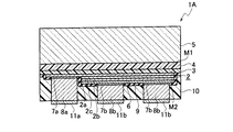
図1に示すように、本発明の第1の実施の形態に係る光半導体装置1Aは、第1主面M1及び第2主面M2を有する発光層2と、その第1主面M1上に設けられた接着層3と、その接着層3上に設けられた蛍光層4と、その蛍光層4上に設けられた透光層5と、発光層2の第2主面M2の第1領域に設けられた反射層6と、その第2主面M2の第2領域に設けられた第1電極7aと、反射層6上に設けられた複数の第2電極7bと、第1電極7aに設けられた第1金属ポスト8aと、各第2電極7bに設けられた複数の第2金属ポスト8bと、発光層2の第2主面M2上に各金属ポスト8a、8bを避けて設けられた絶縁層9と、その絶縁層9上に各金属ポスト8a、8bを封止するように設けられた封止層10と、第1金属ポスト8aの端部に設けられた第1金属層11aと、各第2金属ポスト8bの端部に設けられた複数の第2金属層11bとを備えている。
As shown in FIG. 1, the
発光層2は、n型半導体層である第1クラッド層2aと、その第1クラッド層2aより狭面積のp型半導体層である第2クラッド層2bと、それらの第1クラッド層2a及び第2クラッド層2bにより挟持された活性層2cとにより構成されている。発光層2の厚さは5μmである。この発光層2は、例えば青色光を発光するInGaN層により形成されている。なお、第1主面M1は第1クラッド層2aの上面(図1中)であり、第2主面M2は第1クラッド層2aの下面(図1中)及び第2クラッド層2bの下面(図1中)であり、途中に段差を有している。
The light-emitting
図2に示すように、第1クラッド層2aの平面形状は、一辺550μmの正方形である(図2点線参照)。この第1クラッド層2aの下面(図1中)には、活性層2cを間にして、第1クラッド層2aのコーナ領域(一辺150μmの正方形)を除く領域に第2クラッド層2bが形成されている。なお、活性層2cは第2クラッド層2bと同じ形状をしており、同程度の面積を有している。
As shown in FIG. 2, the planar shape of the
接着層3はシリコーン樹脂により形成されている。接着層3の厚さは例えば1μm以下である。この接着層3は発光層2の第1クラッド層2aの第1主面M1と蛍光層4とを接着する。シリコーン樹脂は、屈折率が1.5程度のメチルフェニルシリコーンである。蛍光体粒子を封止する樹脂には、メチルフェニルシリコーンの他に、ジメチルシリコーン等、他の組成のシリコーン樹脂でもよく、また、輝度が低く、青色光による劣化を受けない場合には、エポキシ樹脂や、エポキシ樹脂とシリコーン樹脂のハイブリット樹脂、もしくはウレタン樹脂等、用途に応じて適時、適切な樹脂が用いられても良い。
The
蛍光層4は、青色光を長波長光に変換する蛍光体粒子を混合したシリコーン樹脂により形成されている。蛍光層4の厚さは例えば15μmである。シリコーン樹脂は、接着層3と同種の樹脂、屈折率が1.5程度のメチルフェニルシリコーンであるが、これに限られるものではなく、他種の樹脂であってもよい。蛍光体は、アルミン酸イットリウムに賦活剤としてセリウムを導入したYAG:Ceであり、その粒子径は10μm以下程度である。蛍光体としては、その他、珪酸ストロンチウム・バリウムに賦活剤としてユーロピウムを導入した(Sr,Ba)2SiO4、Cap(Si,Al)12等を適宜用いることができる。また、混合する蛍光体は1組成である必要はなく、青色光を緑色光と赤色光に波長変換する2種類の蛍光体が混合されて用いられても良い。
The
透光層5は光学ガラスや石英等の透明基材により形成されている。透光層5の厚さは例えば200μmである。この透光層5の材料としては、透明基材に限られるものではなく、その他の透光材料が用いられてもよく、透光性を有する無機物である透光基材が用いられる。ただし、透光基材としては、光半導体装置1Aの光取り出し効率の観点から、屈折率が1.0〜2.0の範囲で可能な限り小さい基材が用いられることが望ましい。これにより、蛍光層4と空気との屈折率差が緩和されるので、光半導体装置1Aの光取り出し効率を向上させることができる。
The
反射層6はAgやAl等の金属により形成されている。反射層6の厚さは例えば0.3μmである。この反射層6は、発光層2の第2クラッド層2bの下面(図1中)の全領域(第1領域)に設けられている。詳しくは、第2クラッド層2bの下面には、0.1μm/0.1μmの厚さでNi/Au等の金属によりNi/Auのコンタクト電極(図示せず)が形成され、その上に厚さ0.3μmの反射層6が形成されている。
The
第1電極7aは0.1μm/0.1μmの厚さでNi/Au等の金属により形成されている。第1電極7aの厚さは0.2μmである。この第1電極7aは、発光層2の第1クラッド層2aの下面(図1中)の露出領域(第2領域)に直径100μmの円形状に設けられている(図2参照)。
The
各第2電極7bも0.1μm/0.1μmの厚さでNi/Au等の金属により形成されている。各第2電極7bの厚さは0.2μmである。これらの第2電極7bは、反射層6の下面(図1中)に直径100μmの円形状に200μmピッチで設けられている(図2参照)。
Each
第1金属ポスト8aはCu等の金属により円柱状に形成されている。第1金属ポスト8aの高さは103μm程度であり、その直径は100μmである。この第1金属ポスト8aは第1電極7aに通電している。なお、第1電極7a及び第1金属ポスト8aの形状は適宜変更可能である。
The
各第2金属ポスト8bはそれぞれCu等の金属により円柱状に形成されている。第2金属ポスト8bの高さは100μmであり、その直径は100μmである。この第2金属ポスト8bは第2電極7bに通電している。各第2金属ポスト8bは、各第2電極7bの配置と同様に200μmピッチで設けられている(図2参照)。なお、第2電極7b及び第2金属ポスト8bの形状は適宜変更可能である。
Each
絶縁層9はSiO2層により形成されており、パッシベーション膜(保護膜)として機能する。絶縁層9の厚さは0.3μmである。絶縁層9は、発光層2をその端部まで完全に覆っており、第1電極7a及び各第2電極7bを除いて外部との通電を防止している。これにより、実装用はんだの這い上がりによるショート等を防ぐことができる。
The insulating
封止層10は熱硬化性樹脂により形成されている。封止層10の厚さは各金属ポスト8a、8bと同様に100μm程度である。封止層10は、第1金属ポスト8aの端部及び各第2金属ポスト8bの端部を露出させて第1金属ポスト8a及び各第2金属ポスト8bを封止するように絶縁層9の全面に設けられている。これにより、第1金属ポスト8a及び各第2金属ポスト8bの周面は封止層10により完全に覆われている。
The
なお、絶縁層9は発光層2をその端部まで完全に覆うように設けられているが、これに限られるものではなく、封止層10が絶縁層9にかわって発光層2をその端部まで完全に覆うように設けられてもよい。この場合でも、第1電極7a及び各第2電極7bを除いて外部との通電が防止されるので、実装用はんだの這い上がりによるショート等を防ぐことができる。
The insulating
第1金属層11a及び各第2金属層11bは、それぞれ1.0μm/0.1μmの厚さでNi/Au等の金属により形成されている。第1金属層11aは第1金属ポスト8aの端部、すなわち露出部分に設けられている。各第2金属層11bはそれぞれ各第2金属ポスト8bの端部、すなわち露出部分に設けられている。なお、第1金属層11aは第1電極7aと同じ円形状となり、第2金属層11bは第2電極7bと同じ円形状となる(図2参照)。
The
このような光半導体装置1Aでは、第1金属ポスト8a及び各第2金属ポスト8bに電圧が印加されると、第1金属ポスト8aから第1クラッド層2aに電位が与えられ、各第2金属ポスト8bから第2クラッド層2bに電位が与えられ、第1クラッド層2aと第2クラッド層2bとに挟まれた活性層2cから光が放射される。放射された光の一部は、透光層5を透過してそのまま透光層5の表面から放出され、他の一部は、反射層6により反射されて透光層5を透過して透光層5の表面から放出される。また、放射された光の一部は蛍光層4に含有される蛍光体粒子に入射するため、蛍光体粒子は励起されて光を放射する。蛍光体粒子による光の一部も透光層5を透過して透光層5の表面から放出され、また、その光の他の一部も、反射層6により反射されて透光層5を透過して透光層5の表面から放出される。このようにして、発光層2により放射された青色光と、その光により励起された蛍光体粒子により放射された光(黄色、あるいは、赤色及び緑色)とは混合され、白色光として透光層5の表面から放出される。
In such an
前述のような構造によれば、装置構成が簡略化されており、発光層2の平面積と同サイズの小型な光半導体装置1Aを得ることができる。さらに、製造時、モールド成形やマウント工程、接続工程等を行う必要がなくなり、通常の半導体製造装置による製造が可能になるので、コストを抑えることができる。また、発光層2上に青色光を長波長光に波長変換する蛍光層4を形成し、発光層2の下面(図1中)に反射層6を形成して上方向にのみ青色光を発光することによって、光半導体装置1Aの上面方向(図1中)に白色光を発光することができる。また、蛍光層4上に透光層5を形成することにより、蛍光層4と空気との屈折率差を緩和することが可能になるので、光の取り出し効率を向上させることができる。また、前述のような構造によれば、発光層2の平面積と同サイズの光半導体装置1Aを一般的な配線基板であるガラスエポキシ基板に実装する場合にも、ガラスエポキシ基板と発光層2間の線膨張係数差を各金属ポスト8a、8bにより緩和することが可能であるため、光半導体装置1Aの実装時の信頼性を確保することができる。
According to the structure as described above, the device configuration is simplified, and a small
以上説明したように、本発明の第1の実施の形態によれば、発光層2上に蛍光層4を設け、その蛍光層4上に透光性を有する無機物を透光層5として設け、さらに、発光層2の第1電極7a上に第1金属ポスト8aを設け、発光層2の各第2電極7b上に第2金属ポスト8bを設け、それらの第1金属ポスト8a及び各第2金属ポスト8bを封止する封止層10を発光層2上に設けることによって、前述の構造の光半導体装置1Aが得られる。この光半導体装置1Aによれば、透光層5が無機物であるため、発光層2から放射された光(特に、青色光)による透光層5の劣化が防止されるので、寿命低下を抑止することができる。さらに、装置構成が簡略化されて製造コストが抑えられるので、低コスト化を実現することができる。加えて、装置構成が簡略化されて装置の平面サイズは発光層2の平面積と同程度になっているので、通常の光半導体素子と同程度に光半導体装置1Aを小型化することができる。
As described above, according to the first embodiment of the present invention, the
(第2の実施の形態)
本発明の第2の実施の形態について図3を参照して説明する。本発明の第2の実施の形態では、第1の実施の形態と異なる部分について説明する。なお、第2の実施の形態においては、第1の実施の形態で説明した部分と同一部分を同一符号で付し、その説明を省略する。
(Second Embodiment)
A second embodiment of the present invention will be described with reference to FIG. In the second embodiment of the present invention, only parts different from the first embodiment will be described. In the second embodiment, the same parts as those described in the first embodiment are denoted by the same reference numerals, and the description thereof is omitted.
図3に示すように、本発明の第2の実施の形態に係る光半導体装置1Bでは、第1金属層11a及び各第2金属層11bがはんだバンプである。すなわち、直径100μmの半球状のはんだバンプが第1金属ポスト8a及び各第2金属ポスト8b上に形成されている。はんだバンプの組成は、Sn−3.0Ag−0.5CuやSn−0.8Cu、Sn−3.5Ag等の表面実装に使用されるはんだ材である。
As shown in FIG. 3, in the
以上説明したように、本発明の第2の実施の形態によれば、第1の実施の形態と同様の効果を得ることができる。さらに、第1金属層11a及び各第2金属層11bをはんだバンプにより形成することによって、光半導体装置1Bが配線基板に実装された場合、第1の実施の形態に係る光半導体装置1Aと比較して、光半導体装置1Bと配線基板とのギャップがはんだバンプにより高くなるので、熱時に線膨張係数差により発生する応力をより緩和することができる。
As described above, according to the second embodiment of the present invention, the same effect as in the first embodiment can be obtained. Furthermore, when the
(第3の実施の形態)
本発明の第3の実施の形態について図4及び図5を参照して説明する。本発明の第3の実施の形態では、第1の実施の形態と異なる部分について説明する。なお、第3の実施の形態においては、第1の実施の形態で説明した部分と同一部分を同一符号で付し、その説明を省略する。
(Third embodiment)
A third embodiment of the present invention will be described with reference to FIGS. In the third embodiment of the present invention, parts different from the first embodiment will be described. In the third embodiment, the same parts as those described in the first embodiment are denoted by the same reference numerals, and the description thereof is omitted.
図4及び図5に示すように、本発明の第3の実施の形態に係る光半導体装置1Cでは、第1クラッド層2aの下面(図4中)に一辺100μmの正方形の第1電極7aが形成され、第2クラッド層2bの下面(図4中)の第2電極7bは、一辺500μmの正方形で、第1クラッド層2aのコーナ領域で一辺150μmの正方形領域分欠けている。第1金属ポスト8aは第1電極7aと同じ平面形状で直方体状の角柱となり、第2金属ポスト8bは第2電極7bと同じ平面形状で角柱となる。さらに、第1金属層11aは第1電極7aと同じ平面形状となり、第2金属層11bは第2電極7bと同じ平面形状となる(図5参照)。
As shown in FIGS. 4 and 5, in the optical semiconductor device 1C according to the third embodiment of the present invention, the square
以上説明したように、本発明の第3の実施の形態によれば、第1の実施の形態と同様の効果を得ることができる。さらに、第1の実施の形態に係る光半導体装置1Aと比較して、第1電極7a及び第2電極7bの平面積を大きく、すなわち、第1金属ポスト8a及び第2金属ポスト8bを大きくすることによって、発光により発熱した熱を逃がすための放熱経路が大きくなるので、熱抵抗の低減により、電流投入時の発熱量を減少させることができると共に、過渡熱抵抗を大幅に減少させることができる。
As described above, according to the third embodiment of the present invention, the same effect as in the first embodiment can be obtained. Furthermore, compared with the
(第4の実施の形態)
本発明の第4の実施の形態について図6を参照して説明する。本発明の第4の実施の形態では、第1の実施の形態と異なる部分について説明する。なお、第4の実施の形態においては、第1の実施の形態で説明した部分と同一部分を同一符号で付し、その説明を省略する。
(Fourth embodiment)
A fourth embodiment of the present invention will be described with reference to FIG. In the fourth embodiment of the present invention, parts different from the first embodiment will be described. In the fourth embodiment, the same parts as those described in the first embodiment are denoted by the same reference numerals, and the description thereof is omitted.
図6に示すように、本発明の第4の実施の形態に係る光半導体装置1Dにおいては、接着層3が除かれており、発光層2の第1主面M1上に蛍光層4が形成されている。蛍光層4の厚さは10μmである。蛍光層4はスパッタ法やCVD(化学気相成長)法等により発光層2の第1主面M1上に形成される。また、透光層5は、例えば、液状ガラスが蛍光層4上にスピンコートにより供給され、その液状ガラスが硬化されて蛍光層4上に形成される。
As shown in FIG. 6, in the optical semiconductor device 1 </ b> D according to the fourth embodiment of the present invention, the
以上説明したように、本発明の第4の実施の形態によれば、第1の実施の形態と同様の効果を得ることができる。さらに、前述のような構造によれば、第1の実施の形態に係る光半導体装置1Aと比較して、製造工程において、蛍光体粒子とシリコーン樹脂とを調合する工程や発光層2と蛍光層4とを接着する工程を排除することが可能になるので、工程の短縮及び低コスト化を実現することができる。
As described above, according to the fourth embodiment of the present invention, the same effect as that of the first embodiment can be obtained. Furthermore, according to the structure as described above, compared with the
(第5の実施の形態)
本発明の第5の実施の形態について図7を参照して説明する。本発明の第5の実施の形態では、第1の実施の形態と異なる部分について説明する。なお、第5の実施の形態においては、第1の実施の形態で説明した部分と同一部分を同一符号で付し、その説明を省略する。
(Fifth embodiment)
A fifth embodiment of the present invention will be described with reference to FIG. In the fifth embodiment of the present invention, parts different from the first embodiment will be described. In the fifth embodiment, the same parts as those described in the first embodiment are denoted by the same reference numerals, and the description thereof is omitted.
図7に示すように、本発明の第5の実施の形態に係る光半導体装置1Eでは、接着層3が除かれており、発光層2の第1主面M1上に蛍光層4として2層の蛍光層4a、4bが形成されている。まず、青色光を緑色光に波長変換する蛍光層4aが形成されており、その上に、青色光を赤色光に波長変換する組成の異なる蛍光層4bが形成されている。各蛍光層4a、4bの厚さはそれぞれ10μmである。これらの蛍光層4a、4bはスパッタ法やCVD(化学気相成長)法等により発光層2の第1主面M1上に形成される。また、透光層5は、例えば、液状ガラスが蛍光層4b上にスピンコートにより供給され、その液状ガラスが硬化されて蛍光層4上に形成される。
As shown in FIG. 7, in the optical semiconductor device 1 </ b> E according to the fifth embodiment of the present invention, the
以上説明したように、本発明の第5の実施の形態によれば、第1の実施の形態と同様の効果を得ることができる。さらに、前述のような構造によれば、第1の実施の形態に係る光半導体装置1Aと比較して、製造工程において、蛍光体粒子とシリコーン樹脂とを調合する工程や発光層2と蛍光層4とを接着する工程を排除することが可能になるので、工程の短縮及び低コスト化を実現することができる。
As described above, according to the fifth embodiment of the present invention, the same effect as that of the first embodiment can be obtained. Furthermore, according to the structure as described above, compared with the
(第6の実施の形態)
本発明の第6の実施の形態について図8ないし図19を参照して説明する。本発明の第6の実施の形態では、第1の実施の形態に係る光半導体装置1Aの製造方法について説明する。なお、この製造方法は、第3の実施の形態に係る光半導体装置1Cの製造方法にも適用される。第6の実施の形態においては、第1の実施の形態で説明した部分と同一部分を同一符号で付し、その説明を省略する。
(Sixth embodiment)
A sixth embodiment of the present invention will be described with reference to FIGS. In the sixth embodiment of the present invention, a method for manufacturing the
まず、図8に示すように、直径2インチで厚さ200μmのサファイアウエハである基板11上にInGaNの青色発光の発光層12が形成される。この発光層12は、まず元となる発光層がエピタキシャル成長により成膜され、その発光層がRIE(反応性イオンエッチング)処理により個別化されている。これにより、光半導体装置1Aの発光層2が形成される。この発光層2は、一辺550μmの正方形領域に第1クラッド層2aが成膜され、その第1クラッド層2aの下面に活性層2cを挟んで、第1クラッド層2aのコーナ領域(一辺150μmの正方形)を除く領域に第2クラッド層2bが成膜されて形成されている(図1及び図2参照)。
First, as shown in FIG. 8, a blue
次に、図9に示すように、基板11上の各発光層12上に多層膜13が形成される。まず、0.1μm/0.1μm厚さのNi/Au膜(図示せず)が発光層12のコンタクト層として発光層12の表面全体にスパッタにより成膜され、その膜上にAgもしくはAlの金属膜(図示せず)が0.3μmの厚さでスパッタ法により成膜される。これにより、光半導体装置1Aの反射層6が形成される。その後、0.1μm/0.1μmの厚さのNi/Au膜(図示せず)が電極材料として発光層12の電極部分に成膜され、電極部分以外の領域に厚さ0.3μmのSiO2膜のパシベーション膜(図示せず)がスパッタ法により成膜される。これにより、光半導体装置1Aの第1電極7a、各第2電極7b及び絶縁層9が形成される。このようにして、基板11上の各発光層2上に多層膜13が形成される。
Next, as shown in FIG. 9, a
次に、図10に示すように、基板11の全面にわたって、メッキの給電層となる導電性膜であるシード層14が蒸着法やスパッタ法などの物理的被着法により形成される。このシード層14としては、例えばTi/Cuなどの積層膜が用いられる。ここで、Ti層はレジストやパッドとの密着強度を高める目的で形成される。したがって、その膜厚は0.1μm程度で構わない。一方、Cuは主に給電に寄与するため、その膜厚は0.2μm以上が好ましい。
Next, as shown in FIG. 10, a
次いで、図11に示すように、基板11の全面にわたって、第1電極7a及び各第2電極7b部分である電極パッド部分を開口した犠牲層であるレジスト層15が形成される。レジストとしては、感光性の液状レジストやドライフィルムレジストを用いることが可能である。レジスト層15は、まず元となるレジスト層が形成された後、開口部を形成するための遮光マスクが用いられ、露光及び現像により開口部が形成されて、基板11の全面に形成される。現像後のレジストはその材料に応じて必要があればベーキングされる。
Next, as shown in FIG. 11, a resist layer 15, which is a sacrificial layer in which electrode pad portions that are the
続いて、図12に示すように、電気メッキ法によりメッキ層16がレジスト層15の開口部に形成される。これにより、光半導体装置1Aの各金属ポスト8a、8bが形成される。電気メッキに際しては、例えば、硫酸銅と硫酸からなるメッキ液中にウエハの基板11が浸漬されるとともに、シード層14に直流電源の負極が接続され、基板11の被メッキ面と対向するように設置したアノードとなるCu板に直流電源の陽極が接続されて電流が流されてCuメッキが開始される。メッキ膜は時間の経過とともにその厚さが増加するが、レジスト層15の厚さに達する前に、通電が停止されてメッキが完了する。
Subsequently, as shown in FIG. 12, a
メッキ後、図13に示すように、レジスト層15が基板11から剥離されて除去される。その後、酸洗浄により、シード層14がエッチングにより除去される。これにより、発光層12、多層膜13及びメッキ層16が露出する。
After plating, as shown in FIG. 13, the resist layer 15 is peeled off from the
次に、図14に示すように、基板11の全面にわたって、封止層となる熱硬化樹脂層17が形成される。まず、スピンコートにより、メッキ層16が埋まる程度の厚さで、メッキ層16の周囲に熱硬化性樹脂が供給され、その後、オーブンに投入され、加熱により熱硬化樹脂層17が硬化する。樹脂は、例えば150℃で2時間の加熱により硬化する。
Next, as shown in FIG. 14, a
その後、図15に示すように、熱硬化樹脂層17の表面が研削されてメッキ層16が露出する。これにより、光半導体装置1Aの封止層10が形成される。熱硬化樹脂層17の研削には、回転研磨ホイールが用いられ、回転研削によって平坦性を確保しながら研削を完了させることが可能である。研削完了後に、必要に応じて、乾燥が行われてもよい。この研削工程は、前工程でスピンコートなどによりメッキ層16の端部のみを露出させて熱硬化樹脂を塗布することは困難であるため(塗布時間及びコストがかかる)、スピンコート後にメッキ層16の端部を露出させるために必要な工程である。
Thereafter, as shown in FIG. 15, the surface of the
次に、図16に示すように、基板11と発光層12との層間にレーザが照射され、基板11から発光層12がリフトオフされる。これにより、発光層12、多層膜13及びメッキ層16及び熱硬化樹脂層17からなる発光基材12Aが基板11から分離される。リフトオフは、Nd:YAGの第三調波レーザを用いて発光層12との層間に基板11を通して波長355nmのレーザ光を照射することによって行われる。なお、リフトオフはオプションであり、省くことも可能である。
Next, as shown in FIG. 16, laser is irradiated between the
次いで、図17に示すように、リフトオフにより形成された発光基材12Aは、光学ガラスウエハ等の透光基材18に設けられた蛍光層19上に発光層12を向けて接着層20を介して貼り合わされる。なお、別工程において蛍光基材が形成され、すなわち、透光性を有する無機物からなる透光基材18上に蛍光体粒子を混合したシリコーン樹脂層が蛍光層19として形成され、そのシリコーン樹脂層上にシリコーン樹脂層が接着層20として形成される。このようにして、光半導体装置1Aの透光層5、蛍光層4及び接着層3が形成される。
Next, as shown in FIG. 17, the light emitting
ここで、蛍光体粒子とシリコーン樹脂は、自公転式の混合装置で均一に混ぜ合わせた後、透光基材18上にスピンコートにより供給され、その後、オーブンに投入されて硬化したものである。シリコーン樹脂としては、例えば150℃で1時間の加熱により硬化するものが用いられる。均一厚さの蛍光層4を成膜するためには、シリコーン樹脂が透光基材18上に供給された後、スペーサが形成され、表面に剥離性の高いフッ素加工を施した冶具が貼り合わされて硬化させられる。これにより、樹脂の表面張力による表面の湾曲を抑制して、均一厚さのシリコーン樹脂膜を成膜することが可能である。
Here, the phosphor particles and the silicone resin are uniformly mixed by a self-revolving mixing device, then supplied onto the light-transmitting
また、蛍光体を混合したシリコーン樹脂層である蛍光層19と発光層12との貼り合わせは、蛍光層19(あるいは発光層12)上にシリコーン樹脂をスプレー工法により供給し、その後、位置合わせ後に貼り合わせを行い、貼り合わせ状態の発光基材12A及び透光基材18をオーブンに投入し、硬化及び接着することによって行われる。シリコーン樹脂の硬化は例えば150℃で1時間の加熱により可能である。
In addition, the
次に、図18に示すように、Ni/Au層21が無電解メッキ法によりメッキ層16のCu電極上に形成される。これにより、光半導体装置1Aの金属層11a、11bが形成される。Niの無電解メッキに際しては、例えば、弱アリカリ性の脱脂液での3分間処理により脱脂が行われ、流水での1分間処理により水洗が行われ、酸洗の後、70℃に温調されたニッケル−リンメッキ液中にウエハが浸漬された後、水洗が行われることにより、Ni層の成膜が実行される。さらに、Auの無電解メッキに際しては、70℃に温調された無電解金メッキ液中にウエハが浸漬された後、水洗及び乾燥が行われることにより、Cu電極表面にメッキが施される。
Next, as shown in FIG. 18, a Ni /
最後に、図19に示すように、ダイサによりダイシングが行われることにより、複数の光半導体装置1Aが切り出され、第1の実施の形態に係る光半導体装置1Aが得られる。なお、第3の実施の形態に係る光半導体装置1Cの製造工程においては、前述と同一の工程が用いられ、レジスト層15の開口サイズ及び形状の変更により、第3の実施の形態に係る光半導体装置1Cが得られる。
Finally, as shown in FIG. 19, by dicing with a dicer, a plurality of
以上説明したように、本発明の第6の実施の形態によれば、第1の実施の形態に係る光半導体装置1Aを製造することができ、その結果、第1の実施の形態と同様の効果を得ることができる。また、レジスト層15の開口サイズ及び形状の変更することによって、第3の実施の形態に係る光半導体装置1Cを製造することができ、その結果、第3の実施の形態と同様の効果を得ることができる。さらに、一度の製造工程で多数の光半導体装置1A、1Cを製造することが可能であるので、光半導体装置1A、1Cの大量生産を実現することができ、その結果、光半導体装置1A、1Cのコストを抑えることができる。
As described above, according to the sixth embodiment of the present invention, the
(第7の実施の形態)
本発明の第7の実施の形態について図20ないし図23を参照して説明する。本発明の第7の実施の形態では、第2の実施の形態に係る光半導体装置1Bの製造方法について説明する。なお、第7の実施の形態においては、第2の実施の形態で説明した部分と同一部分を同一符号で付し、その説明を省略する。
(Seventh embodiment)
A seventh embodiment of the present invention will be described with reference to FIGS. In the seventh embodiment of the present invention, a method for manufacturing an
本発明の第7の実施の形態に係る製造工程は、図8に示す発光層12の成膜工程から図17に示す貼り合わせ工程まで第6の実施の形態と同じ工程を有している。
The manufacturing process according to the seventh embodiment of the present invention includes the same processes as those of the sixth embodiment from the film forming process of the
貼り合わせ工程後、図20に示すように、メッキ層16のCu電極上にNi/Au層などのコンタクト層31が無電解メッキ法により形成される。Niの無電解メッキ及びAuの無電解メッキに際しては、第6の実施の形態に係るNi/Au層21の形成工程と同様のメッキが行われる。
After the bonding step, as shown in FIG. 20, a
次に、図21に示すように、Sn−3.0Ag−0.5Cuのはんだペースト32が印刷法によりコンタクト層31上に塗布される。なお、はんだペースト32の塗布方法は印刷法に限られるものではない。
Next, as shown in FIG. 21, a
その後、図22に示すように、ウエハの透光基材18がリフリー炉に通されてはんだが再溶融され、フラックス残渣が洗浄されることにより、はんだバンプ33がメッキ層16のCu電極上に形成される。これにより、光半導体装置1Bの金属層11a、11bが形成される。
Thereafter, as shown in FIG. 22, the
最後に、図23に示すように、ダイサによりダイシングが行われることにより、複数の光半導体装置1Bが切り出され、第2の実施の形態に係る光半導体装置1Bが得られる。
Finally, as shown in FIG. 23, dicing is performed by a dicer, whereby a plurality of
以上説明したように、本発明の第7の実施の形態によれば、第2の実施の形態に係る光半導体装置1Bを製造することができ、その結果、第2の実施の形態と同様の効果を得ることができる。さらに、一度の製造工程で多数の光半導体装置1Bを製造することが可能であるので、光半導体装置1Bの大量生産を実現することができ、その結果、光半導体装置1Bのコストを抑えることができる。
As described above, according to the seventh embodiment of the present invention, the
(第8の実施の形態)
本発明の第8の実施の形態について図24ないし図27を参照して説明する。本発明の第8の実施の形態では、第4の実施の形態に係る光半導体装置1Dの製造方法について説明する。なお、この製造方法は、第5の実施の形態に係る光半導体装置1Eの製造方法にも適用される。第8の実施の形態においては、第4の実施の形態で説明した部分と同一部分を同一符号で付し、その説明を省略する。
(Eighth embodiment)
An eighth embodiment of the present invention will be described with reference to FIGS. In the eighth embodiment of the present invention, a method for manufacturing an
本発明の第8の実施の形態に係る製造工程は、図8に示す発光層12の成膜工程から図16に示すリフトオフ工程まで第6の実施の形態と同じ工程を有している。
The manufacturing process according to the eighth embodiment of the present invention includes the same processes as those of the sixth embodiment from the film forming process of the
リフトオフ工程後、図24に示すように、蛍光層41がスパッタ装置により発光基材12Aの発光層12側の面上に形成される。これにより、光半導体装置1Dの蛍光層4が形成される。このとき、スパッタを複数回行うことにより蛍光層41を積層することも可能であり、第5の実施の形態に係る光半導体装置1Eを製造することができる。なお、蛍光層41は、CVD装置を用いて成膜することも可能である。
After the lift-off process, as shown in FIG. 24, the
次に、図25に示すように、蛍光層41上に液状ガラスがスピンコートにより供給され、その液状ガラスが硬化されて透光層42が蛍光層41上に成膜される。これにより、光半導体装置1Dの透光層5が形成される。液状ガラスは、スピンコートの他、スプレー工法により供給されることも可能であり、その供給方法は限定されない。ガラス層の硬化は、例えば200℃で1時間の加熱により実施可能である。透光層42の成膜材料としては、液状ガラスの他、用途に応じて適宜選択することが可能である。
Next, as shown in FIG. 25, liquid glass is supplied onto the
次に、図26に示すように、メッキ層16のCu電極上にNi/Au層43が無電解メッキ法により形成される。これにより、光半導体装置1Dの金属層11a、11bが形成される。Niの無電解メッキ及びAuの無電解メッキに際しては、第6の実施の形態に係るNi/Au層21の形成工程と同様のメッキが行われる。
Next, as shown in FIG. 26, a Ni /
最後に、図27に示すように、ダイサによりダイシングが行われることにより、複数の光半導体装置1Dが切り出され、第4の実施の形態に係る光半導体装置1Dが得られる。なお、第5の実施の形態に係る光半導体装置1Eの製造工程においては、前述と同一の工程が用いられ、蛍光層41の形成工程でスパッタを複数回行って蛍光層41を積層することにより、第5の実施の形態に係る光半導体装置1Eが得られる。
Finally, as shown in FIG. 27, dicing is performed by a dicer, whereby a plurality of
以上説明したように、本発明の第8の実施の形態によれば、第4の実施の形態に係る光半導体装置1Dを製造することができ、その結果、第4の実施の形態と同様の効果を得ることができる。また、蛍光層41を積層することによって、第5の実施の形態に係る光半導体装置1Eを製造することができ、その結果、第5の実施の形態と同様の効果を得ることができる。さらに、一度の製造工程で多数の光半導体装置1D、1Eを製造することが可能であるので、光半導体装置1D、1Eの大量生産を実現することができ、その結果、光半導体装置1D、1Eのコストを抑えることができる。
As described above, according to the eighth embodiment of the present invention, the
(他の実施の形態)
なお、本発明は、前述の実施の形態に限るものではなく、その要旨を逸脱しない範囲において種々変更可能である。例えば、前述の実施の形態に示される全構成要素から幾つかの構成要素を削除してもよい。さらに、異なる実施の形態に亘る構成要素を適宜組み合わせてもよい。また、前述の実施の形態においては、各種の数値を挙げているが、それらの数値は例示であり、限定されるものではない。
(Other embodiments)
The present invention is not limited to the above-described embodiment, and various modifications can be made without departing from the scope of the invention. For example, some components may be deleted from all the components shown in the above-described embodiment. Furthermore, you may combine the component covering different embodiment suitably. Moreover, in the above-mentioned embodiment, although various numerical values are mentioned, those numerical values are illustrations and are not limited.
1A〜1D…光半導体装置、2…発光層、4…蛍光層、5…透光層、7a…第1電極、7b…第2電極、8a…第1金属ポスト、8b…第2金属ポスト、10…封止層、11a…第1金属層、11b…第2金属層、M1…第1主面、M2…第2主面、11…基板、12…発光層12A…発光基材、、14…導電性膜(シード層)、15…犠牲層(レジスト層)、16…メッキ層、17…封止層(熱硬化樹脂層)、18…透光基材、19,41…蛍光層、21,33,43…金属層、42…透光層
DESCRIPTION OF
Claims (7)
前記第1クラッド層の形状の一部が除かれた形状のp型半導体からなる第2クラッド層と、
前記第1及び第2クラッド層に挟持された前記第2クラッド層と同形状の活性層と、
前記第1クラッド層の前記活性層が設けられた側と反対側の面に形成され、平面視で前記第1及び第2クラッド層と前記活性層のいずれよりも周囲にはみだしており、前記活性層から放出される光を吸収して異なる波長の光を放出する蛍光体を含む蛍光層と、
前記第1クラッド層の前記活性層が設けられた面側の前記活性層及び前記第2クラッド層が除かれた領域に形成された第1電極と、
前記第2クラッド層の前記活性層が設けられた側と反対側の面に形成された第2電極と、
前記第1電極上に設けられた第1金属ポストと、
前記第2電極上に設けられた第2金属ポストと、
前記第1クラッド層と前記活性層と前記第2クラッド層の側面を覆い前記蛍光層に至る絶縁層と、
前記第1及び第2クラッド層の前記第1及び第2金属ポストが設けられている側に設けられ、前記絶縁層を介して前記第1クラッド層と前記活性層と前記第2クラッド層の前記側面を覆い、前記第1及び第2金属ポストの端部を露出させて前記第1及び第2金属ポストを封止する封止層と、
を備えたことを特徴とする光半導体装置。 a first cladding layer made of an n-type semiconductor;
A second cladding layer made of a p-type semiconductor having a shape obtained by removing a part of the shape of the first cladding layer;
An active layer having the same shape as the second cladding layer sandwiched between the first and second cladding layers;
It is formed on the surface of the first cladding layer opposite to the side on which the active layer is provided, and protrudes from the periphery of any of the first and second cladding layers and the active layer in plan view. A fluorescent layer comprising a phosphor that absorbs light emitted from the layer and emits light of different wavelengths;
A first electrode formed in a region where the active layer and the second cladding layer on the surface side of the first cladding layer where the active layer is provided;
A second electrode formed on the surface of the second cladding layer opposite to the side on which the active layer is provided;
A first metal post provided on the first electrode;
A second metal post provided on the second electrode;
An insulating layer covering side surfaces of the first cladding layer, the active layer, and the second cladding layer and reaching the fluorescent layer;
The first and second cladding layers are provided on the side where the first and second metal posts are provided, and the first cladding layer, the active layer, and the second cladding layer are interposed through the insulating layer. A sealing layer that covers a side surface and exposes the ends of the first and second metal posts to seal the first and second metal posts;
An optical semiconductor device comprising:
前記導電性膜上に、前記発光層ごとの前記第1電極及び前記第2電極上を開口する犠牲層を形成する工程と、
前記導電性膜を陰極として電気メッキ法により前記発光層ごとの前記第1電極及び前記第2電極上にメッキ層を形成する工程と、
前記メッキ層を形成した前記基板から前記犠牲層及び前記導電性膜を除去する工程と、
前記犠牲層及び前記導電性膜を除去した前記基板上に、前記発光層ごとの前記メッキ層を封止する封止層を形成する工程と、
前記封止層から前記発光層ごとの前記メッキ層の端部を露出させる工程と、
前記封止層の上に支持基板を貼り付けずに、前記封止層と前記メッキ層とを含む支持体により前記発光層が支持された状態で前記発光層を前記基板から分離する工程と、
透光性を有する透光基材上に、前記発光層から放出される光を吸収して異なる波長の光を放出する蛍光体を含む蛍光層を形成する工程と、
前記蛍光層を形成した前記透光基材を前記基板から分離した前記複数の発光層に前記蛍光層を対向させて接合する工程と、
前記発光層ごとに個片化を行う工程と、
を備えたことを特徴とする光半導体装置の製造方法。 A plurality of light emitting layers made of a semiconductor epitaxially grown on a substrate is formed, and the plurality of light emitting layers are formed on the substrate on which the first electrode and the second electrode are formed on each of the plurality of light emitting layers. Forming a covering conductive film;
Forming a sacrificial layer opening on the first electrode and the second electrode for each of the light emitting layers on the conductive film;
Forming a plating layer on the first electrode and the second electrode for each light emitting layer by electroplating using the conductive film as a cathode;
Removing the sacrificial layer and the conductive film from the substrate on which the plating layer is formed;
Forming a sealing layer for sealing the plating layer for each light emitting layer on the substrate from which the sacrificial layer and the conductive film have been removed;
Exposing the end of the plating layer for each light emitting layer from the sealing layer;
Separating the light emitting layer from the substrate in a state in which the light emitting layer is supported by a support including the sealing layer and the plating layer without attaching a support substrate on the sealing layer;
Forming a fluorescent layer containing a phosphor that absorbs light emitted from the light emitting layer and emits light of a different wavelength on a light transmissive substrate having translucency;
Bonding the fluorescent layer to the plurality of light-emitting layers separated from the substrate, the light-transmitting base material on which the fluorescent layer is formed; and
Singulation for each light emitting layer;
An optical semiconductor device manufacturing method comprising:
前記基板から分離した前記発光層の前記第2主面とは反対側の第1主面側に、前記発光層から放出される光を吸収して異なる波長の光を放出する蛍光体を含む蛍光層を形成する工程と、
前記正極及び負極ごとに個片化を行う工程と、
を備えたことを特徴とする光半導体装置の製造方法。 A plurality of sets of a positive electrode and a negative electrode, which are formed on the second main surface side of the light emitting layer opposite to the substrate, and through which current is emitted to emit light from the light emitting layer, is a semiconductor layer epitaxially grown on the substrate A first metal post provided on each of the positive electrodes, a second metal post provided on each of the negative electrodes, an end of the first metal post provided on the second main surface side, and the A sealing substrate that seals the first metal post and the second metal post by exposing an end portion of the second metal post, and does not attach a support substrate on the sealing layer of the light emitting base material And separating the light emitting layer from the substrate in a state where the light emitting layer is supported by a support including the sealing layer and the first and second metal posts,
Fluorescence including a phosphor that absorbs light emitted from the light emitting layer and emits light of a different wavelength on the first main surface side opposite to the second main surface of the light emitting layer separated from the substrate Forming a layer;
Singulation for each of the positive electrode and the negative electrode;
An optical semiconductor device manufacturing method comprising:
前記導電性膜上に、前記発光層ごとの前記第1電極及び前記第2電極上を開口する犠牲層を形成する工程と、
前記導電性膜を陰極として電気メッキ法により前記発光層ごとの前記第1電極及び前記第2電極上にメッキ層を形成する工程と、
前記メッキ層を形成した前記基板から前記犠牲層及び前記導電性膜を除去する工程と、
前記犠牲層及び前記導電性膜を除去した前記基板上に、前記発光層ごとの前記メッキ層を封止する封止層を形成する工程と、
前記封止層から前記発光層ごとの前記メッキ層の端部を露出させる工程と、
前記封止層の上に支持基板を貼り付けずに、前記封止層と前記メッキ層とを含む支持体により前記発光層が支持された状態で前記複数の発光層を前記基板から分離する工程と、
前記基板から分離した前記複数の発光層上に、前記発光層から放出される光を吸収して異なる波長の光を放出する蛍光体を含む蛍光層を形成する工程と、
前記蛍光層上に、透光性を有する透光層を形成する工程と、
前記発光層ごとに個片化を行う工程と、
を備えたことを特徴とする光半導体装置の製造方法。 A plurality of light emitting layers are formed on a substrate, and a conductive film covering the plurality of light emitting layers is formed on the substrate on which the first electrode and the second electrode are formed on each of the plurality of light emitting layers. And a process of
Forming a sacrificial layer opening on the first electrode and the second electrode for each of the light emitting layers on the conductive film;
Forming a plating layer on the first electrode and the second electrode for each light emitting layer by electroplating using the conductive film as a cathode;
Removing the sacrificial layer and the conductive film from the substrate on which the plating layer is formed;
Forming a sealing layer for sealing the plating layer for each light emitting layer on the substrate from which the sacrificial layer and the conductive film have been removed;
Exposing the end of the plating layer for each light emitting layer from the sealing layer;
A step of separating the plurality of light emitting layers from the substrate in a state where the light emitting layer is supported by a support including the sealing layer and the plating layer without attaching a support substrate on the sealing layer. When,
Forming a fluorescent layer including a phosphor that absorbs light emitted from the light emitting layer and emits light of a different wavelength on the plurality of light emitting layers separated from the substrate;
Forming a translucent layer having translucency on the fluorescent layer;
Singulation for each light emitting layer;
An optical semiconductor device manufacturing method comprising:
Priority Applications (7)
| Application Number | Priority Date | Filing Date | Title |
|---|---|---|---|
| JP2008312453A JP4799606B2 (en) | 2008-12-08 | 2008-12-08 | Optical semiconductor device and method for manufacturing optical semiconductor device |
| EP09169704A EP2194586A1 (en) | 2008-12-08 | 2009-09-08 | Semiconductor device and method for manufacturing the same |
| EP15157374.8A EP2903039B1 (en) | 2008-12-08 | 2009-09-08 | Semiconductor device |
| EP14168448.0A EP2784831A1 (en) | 2008-12-08 | 2009-09-08 | Semiconductor device and method for manufacturing the same |
| US12/556,134 US8581291B2 (en) | 2008-12-08 | 2009-09-09 | Semiconductor device and method for manufacturing the same |
| US14/023,641 US8906716B2 (en) | 2008-12-08 | 2013-09-11 | Semiconductor device and method for manufacturing the same |
| US14/488,032 US9431588B2 (en) | 2008-12-08 | 2014-09-16 | Semiconductor device and method for manufacturing the same |
Applications Claiming Priority (1)
| Application Number | Priority Date | Filing Date | Title |
|---|---|---|---|
| JP2008312453A JP4799606B2 (en) | 2008-12-08 | 2008-12-08 | Optical semiconductor device and method for manufacturing optical semiconductor device |
Publications (3)
| Publication Number | Publication Date |
|---|---|
| JP2010135693A JP2010135693A (en) | 2010-06-17 |
| JP2010135693A5 JP2010135693A5 (en) | 2010-09-02 |
| JP4799606B2 true JP4799606B2 (en) | 2011-10-26 |
Family
ID=42060918
Family Applications (1)
| Application Number | Title | Priority Date | Filing Date |
|---|---|---|---|
| JP2008312453A Active JP4799606B2 (en) | 2008-12-08 | 2008-12-08 | Optical semiconductor device and method for manufacturing optical semiconductor device |
Country Status (3)
| Country | Link |
|---|---|
| US (3) | US8581291B2 (en) |
| EP (3) | EP2784831A1 (en) |
| JP (1) | JP4799606B2 (en) |
Cited By (1)
| Publication number | Priority date | Publication date | Assignee | Title |
|---|---|---|---|---|
| JP2014175543A (en) * | 2013-03-11 | 2014-09-22 | Toshiba Corp | Semiconductor light-emitting device |
Families Citing this family (88)
| Publication number | Priority date | Publication date | Assignee | Title |
|---|---|---|---|---|
| US9000461B2 (en) * | 2003-07-04 | 2015-04-07 | Epistar Corporation | Optoelectronic element and manufacturing method thereof |
| US10686106B2 (en) | 2003-07-04 | 2020-06-16 | Epistar Corporation | Optoelectronic element |
| US9142740B2 (en) | 2003-07-04 | 2015-09-22 | Epistar Corporation | Optoelectronic element and manufacturing method thereof |
| US20110284866A1 (en) * | 2005-01-11 | 2011-11-24 | Tran Chuong A | Light-emitting diode (led) structure having a wavelength-converting layer and method of producing |
| JP4799606B2 (en) * | 2008-12-08 | 2011-10-26 | 株式会社東芝 | Optical semiconductor device and method for manufacturing optical semiconductor device |
| JP4724222B2 (en) | 2008-12-12 | 2011-07-13 | 株式会社東芝 | Method for manufacturing light emitting device |
| JP5414579B2 (en) * | 2009-11-19 | 2014-02-12 | 株式会社東芝 | Semiconductor light emitting device |
| JP5349260B2 (en) * | 2009-11-19 | 2013-11-20 | 株式会社東芝 | Semiconductor light emitting device and manufacturing method thereof |
| CN102884645B (en) * | 2010-01-29 | 2015-05-27 | 西铁城电子株式会社 | Method for producing light-emitting device and light emitting device |
| JP5390472B2 (en) * | 2010-06-03 | 2014-01-15 | 株式会社東芝 | Semiconductor light emitting device and manufacturing method thereof |
| JP4875185B2 (en) * | 2010-06-07 | 2012-02-15 | 株式会社東芝 | Optical semiconductor device |
| JP5343040B2 (en) | 2010-06-07 | 2013-11-13 | 株式会社東芝 | Semiconductor light emitting device |
| JP5426484B2 (en) | 2010-06-07 | 2014-02-26 | 株式会社東芝 | Manufacturing method of semiconductor light emitting device |
| KR101714039B1 (en) * | 2010-07-01 | 2017-03-08 | 엘지이노텍 주식회사 | Light emitting device, method for fabricating the light emitting device, light emitting device package and lighting system |
| US8956922B2 (en) | 2010-09-06 | 2015-02-17 | Heraeus Noblelight Gmbh | Coating method for an optoelectronic chip-on-board module |
| US9070851B2 (en) | 2010-09-24 | 2015-06-30 | Seoul Semiconductor Co., Ltd. | Wafer-level light emitting diode package and method of fabricating the same |
| JP4778107B1 (en) * | 2010-10-19 | 2011-09-21 | 有限会社ナプラ | Light emitting device and manufacturing method thereof |
| JP5537446B2 (en) | 2011-01-14 | 2014-07-02 | 株式会社東芝 | Light emitting device, light emitting module, and method of manufacturing light emitting device |
| JP6110310B2 (en) * | 2011-01-24 | 2017-04-05 | コーニンクレッカ フィリップス エヌ ヴェKoninklijke Philips N.V. | LIGHT EMITTING DEVICE AND LIGHT EMITTING DEVICE MANUFACTURING METHOD |
| KR101761834B1 (en) * | 2011-01-28 | 2017-07-27 | 서울바이오시스 주식회사 | Wafer level led package and method of fabricating the same |
| JP5603793B2 (en) * | 2011-02-09 | 2014-10-08 | 株式会社東芝 | Semiconductor light emitting device |
| JP5603813B2 (en) | 2011-03-15 | 2014-10-08 | 株式会社東芝 | Semiconductor light emitting device and light emitting device |
| JP5498417B2 (en) * | 2011-03-15 | 2014-05-21 | 株式会社東芝 | Semiconductor light emitting device and manufacturing method thereof |
| JP2012195402A (en) * | 2011-03-16 | 2012-10-11 | Toshiba Corp | Manufacturing method for semiconductor light-emitting device |
| US10074778B2 (en) | 2011-03-22 | 2018-09-11 | Seoul Viosys Co., Ltd. | Light emitting diode package and method for manufacturing the same |
| JP5657591B2 (en) | 2011-03-23 | 2015-01-21 | 株式会社東芝 | Semiconductor light emitting device and manufacturing method thereof |
| JP5535114B2 (en) | 2011-03-25 | 2014-07-02 | 株式会社東芝 | Light emitting device, light emitting module, and method of manufacturing light emitting device |
| JP5953386B2 (en) * | 2011-03-28 | 2016-07-20 | 日東電工株式会社 | Method for manufacturing light emitting diode device |
| JP2012216712A (en) * | 2011-03-28 | 2012-11-08 | Nitto Denko Corp | Method for manufacturing light-emitting diode device and light-emitting element |
| JP5745319B2 (en) * | 2011-04-14 | 2015-07-08 | 日東電工株式会社 | Fluorescent reflection sheet and method for manufacturing light emitting diode device |
| JP5777705B2 (en) * | 2011-04-20 | 2015-09-09 | 株式会社エルム | Light emitting device and manufacturing method thereof |
| JP5642623B2 (en) | 2011-05-17 | 2014-12-17 | 株式会社東芝 | Semiconductor light emitting device |
| JP5864367B2 (en) * | 2011-06-16 | 2016-02-17 | 日東電工株式会社 | Fluorescent adhesive sheet, light-emitting diode element with phosphor layer, light-emitting diode device, and manufacturing method thereof |
| JP5394461B2 (en) * | 2011-06-28 | 2014-01-22 | シャープ株式会社 | Method for manufacturing optical semiconductor element |
| CN102856458B (en) * | 2011-06-28 | 2015-05-06 | 夏普株式会社 | Photosemiconductor element and method for manufacturing photosemiconductor element |
| JP2013012559A (en) * | 2011-06-29 | 2013-01-17 | Nichia Chem Ind Ltd | Manufacturing method of light emitting element |
| JP2013021175A (en) * | 2011-07-12 | 2013-01-31 | Toshiba Corp | Semiconductor light-emitting element |
| KR101360482B1 (en) * | 2011-07-15 | 2014-02-24 | 엘지이노텍 주식회사 | The light emitting device package and the method for manufacturing the same |
| KR101283117B1 (en) | 2011-07-15 | 2013-07-05 | 엘지이노텍 주식회사 | The light emitting device package and the method for manufacturing the same |
| JP5662277B2 (en) | 2011-08-08 | 2015-01-28 | 株式会社東芝 | Semiconductor light emitting device and light emitting module |
| US20140198528A1 (en) * | 2011-08-17 | 2014-07-17 | Samsung Electronics Co., Ltd. | Wavelength conversion chip for a light emitting diode, and method for manufacturing same |
| WO2013030690A1 (en) * | 2011-08-30 | 2013-03-07 | Koninklijke Philips Electronics N.V. | Method of bonding a substrate to a semiconductor light emitting device |
| JP2013065726A (en) | 2011-09-16 | 2013-04-11 | Toshiba Corp | Semiconductor light-emitting device and method of manufacturing the same |
| US20130095581A1 (en) * | 2011-10-18 | 2013-04-18 | Taiwan Semiconductor Manufacturing Company, Ltd. | Thick window layer led manufacture |
| KR101969334B1 (en) * | 2011-11-16 | 2019-04-17 | 엘지이노텍 주식회사 | Light emitting device and light emitting apparatus having the same |
| JP2013140942A (en) * | 2011-12-07 | 2013-07-18 | Toshiba Corp | Semiconductor light-emitting device |
| DE102012101409A1 (en) * | 2011-12-23 | 2013-06-27 | Osram Opto Semiconductors Gmbh | Method for producing a plurality of optoelectronic semiconductor chips and optoelectronic semiconductor chip |
| EP2816621A4 (en) * | 2012-02-15 | 2015-10-21 | Panasonic Ip Man Co Ltd | Light emitting apparatus and method for manufacturing same |
| JP5684751B2 (en) | 2012-03-23 | 2015-03-18 | 株式会社東芝 | Semiconductor light emitting device and manufacturing method thereof |
| JP5985322B2 (en) * | 2012-03-23 | 2016-09-06 | 株式会社東芝 | Semiconductor light emitting device and manufacturing method thereof |
| JP2013211399A (en) | 2012-03-30 | 2013-10-10 | Toshiba Corp | Semiconductor light-emitting element |
| JP6006523B2 (en) * | 2012-04-27 | 2016-10-12 | 新光電気工業株式会社 | Connection structure, wiring board unit, electronic circuit component unit, and electronic apparatus |
| JP6263741B2 (en) * | 2012-05-09 | 2018-01-24 | 株式会社Joled | Light emitting device |
| JP2014053506A (en) | 2012-09-07 | 2014-03-20 | Toshiba Corp | Semiconductor light-emitting device and light-emitting module |
| DE102013100711B4 (en) * | 2013-01-24 | 2021-07-01 | OSRAM Opto Semiconductors Gesellschaft mit beschränkter Haftung | Process for the production of a large number of optoelectronic components |
| JP2014175362A (en) | 2013-03-06 | 2014-09-22 | Toshiba Corp | Semiconductor light-emitting element and method of manufacturing the same |
| JP6394052B2 (en) | 2013-05-13 | 2018-09-26 | 日亜化学工業株式会社 | Light emitting device and manufacturing method thereof |
| JP2015012212A (en) * | 2013-07-01 | 2015-01-19 | 株式会社ディスコ | Light-emitting chip |
| CN105340089B (en) * | 2013-07-03 | 2021-03-12 | 亮锐控股有限公司 | LED with stress buffer layer under metallization layer |
| CN105378948B (en) * | 2013-07-18 | 2020-08-28 | 亮锐控股有限公司 | Dicing a wafer of light emitting devices |
| US9954144B2 (en) * | 2014-01-10 | 2018-04-24 | Cree, Inc. | Wafer level contact pad solder bumping for surface mount devices with non-planar recessed contacting surfaces |
| US20150200336A1 (en) * | 2014-01-10 | 2015-07-16 | Cree, Inc. | Wafer level contact pad standoffs with integrated reflector |
| JP6256026B2 (en) | 2014-01-17 | 2018-01-10 | 日亜化学工業株式会社 | LIGHT EMITTING DEVICE AND LIGHT EMITTING DEVICE MANUFACTURING METHOD |
| JP6185415B2 (en) * | 2014-03-27 | 2017-08-23 | 株式会社東芝 | Semiconductor light emitting device |
| EP3143648A4 (en) * | 2014-05-14 | 2017-09-27 | Nanyang Technological University | Method of forming a light-emitting device |
| JP2016033969A (en) * | 2014-07-31 | 2016-03-10 | 株式会社東芝 | Electronic component and electronic unit |
| JP6384202B2 (en) * | 2014-08-28 | 2018-09-05 | 日亜化学工業株式会社 | Method for manufacturing light emitting device |
| WO2016079658A1 (en) | 2014-11-18 | 2016-05-26 | Industries Yifei Wang Inc. | Led module, methods of manufacturing same and luminaire integrating same |
| JP6555907B2 (en) * | 2015-03-16 | 2019-08-07 | アルパッド株式会社 | Semiconductor light emitting device |
| KR20160124375A (en) * | 2015-04-17 | 2016-10-27 | 삼성전자주식회사 | Method of manufacturing semiconductor light emitting device package |
| US10217914B2 (en) * | 2015-05-27 | 2019-02-26 | Samsung Electronics Co., Ltd. | Semiconductor light emitting device |
| DE102015214222A1 (en) * | 2015-07-28 | 2017-02-02 | Osram Opto Semiconductors Gmbh | Method for producing a component and a component |
| DE102015214228A1 (en) | 2015-07-28 | 2017-02-02 | Osram Opto Semiconductors Gmbh | Method for producing a component and a component |
| DE102015214219A1 (en) * | 2015-07-28 | 2017-02-02 | Osram Opto Semiconductors Gmbh | Method for producing a component and a component |
| KR102415331B1 (en) * | 2015-08-26 | 2022-06-30 | 삼성전자주식회사 | light emitting diode(LED) package and apparatus including the same |
| DE102015114583A1 (en) * | 2015-09-01 | 2017-03-02 | Osram Opto Semiconductors Gmbh | Process for the production of optoelectronic semiconductor chips and optoelectronic semiconductor chip |
| CN205944139U (en) | 2016-03-30 | 2017-02-08 | 首尔伟傲世有限公司 | Ultraviolet ray light -emitting diode spare and contain this emitting diode module |
| TWI703744B (en) * | 2016-04-08 | 2020-09-01 | 晶元光電股份有限公司 | Light-emitting device |
| JP2018022781A (en) * | 2016-08-03 | 2018-02-08 | パナソニックIpマネジメント株式会社 | Optical device |
| KR101781748B1 (en) * | 2016-09-01 | 2017-09-25 | 주식회사 루멘스 | Uv led package |
| US11177417B2 (en) * | 2017-02-13 | 2021-11-16 | Nichia Corporation | Light emitting device including phosphor layer with protrusions and recesses and method for manufacturing same |
| JP6645486B2 (en) * | 2017-02-13 | 2020-02-14 | 日亜化学工業株式会社 | Light emitting device and method of manufacturing the same |
| DE102017109485A1 (en) * | 2017-05-03 | 2018-11-08 | Osram Opto Semiconductors Gmbh | Optoelectronic semiconductor chip and method for producing an optoelectronic semiconductor chip |
| CN109712967B (en) * | 2017-10-25 | 2020-09-29 | 隆达电子股份有限公司 | Light emitting diode device and manufacturing method thereof |
| US20190196285A1 (en) * | 2017-12-26 | 2019-06-27 | Shenzhen China Star Optoelectronics Semiconductor Display Technology Co., Ltd. | Manufacturing method of array substrate and its upper electrode line pattern and liquid crystal display panel |
| JP6766900B2 (en) * | 2019-01-15 | 2020-10-14 | 日亜化学工業株式会社 | Light emitting device |
| US11764328B2 (en) * | 2019-08-13 | 2023-09-19 | Epistar Corporation | Light-emitting diode package having bump formed in wriggle shape |
| US20230013841A1 (en) * | 2021-07-16 | 2023-01-19 | Epistar Corporation | Light-emitting device |
Family Cites Families (43)
| Publication number | Priority date | Publication date | Assignee | Title |
|---|---|---|---|---|
| JPH02196477A (en) | 1989-01-25 | 1990-08-03 | Nec Corp | Manufacture of photosemiconductor device |
| EP0921577A4 (en) * | 1997-01-31 | 2007-10-31 | Matsushita Electric Ind Co Ltd | Light emitting element, semiconductor light emitting device, and method for manufacturing them |
| US6340824B1 (en) * | 1997-09-01 | 2002-01-22 | Kabushiki Kaisha Toshiba | Semiconductor light emitting device including a fluorescent material |
| JP2000183407A (en) | 1998-12-16 | 2000-06-30 | Rohm Co Ltd | Optical semiconductor device |
| US6331450B1 (en) * | 1998-12-22 | 2001-12-18 | Toyoda Gosei Co., Ltd. | Method of manufacturing semiconductor device using group III nitride compound |
| JP4045710B2 (en) * | 1999-12-16 | 2008-02-13 | 松下電器産業株式会社 | Manufacturing method of semiconductor light emitting device |
| DE10020465A1 (en) * | 2000-04-26 | 2001-11-08 | Osram Opto Semiconductors Gmbh | Radiation-emitting semiconductor component with luminescence conversion element |
| JP4403422B2 (en) * | 2000-07-18 | 2010-01-27 | ソニー株式会社 | Manufacturing method of image display device |
| JP3589187B2 (en) * | 2000-07-31 | 2004-11-17 | 日亜化学工業株式会社 | Method for forming light emitting device |
| JP2002076434A (en) * | 2000-08-28 | 2002-03-15 | Toyoda Gosei Co Ltd | Light emitting device |
| JP3614776B2 (en) * | 2000-12-19 | 2005-01-26 | シャープ株式会社 | Chip component type LED and its manufacturing method |
| JP4081985B2 (en) * | 2001-03-02 | 2008-04-30 | 日亜化学工業株式会社 | Light emitting device and manufacturing method thereof |
| JP4529319B2 (en) * | 2001-06-27 | 2010-08-25 | 日亜化学工業株式会社 | Semiconductor chip and manufacturing method thereof |
| US6943379B2 (en) * | 2002-04-04 | 2005-09-13 | Toyoda Gosei Co., Ltd. | Light emitting diode |
| JP2004134672A (en) * | 2002-10-11 | 2004-04-30 | Sony Corp | Method and apparatus for manufacturing super-thin semiconductor device and super-thin backlighting type solid-state imaging device |
| US20040188696A1 (en) * | 2003-03-28 | 2004-09-30 | Gelcore, Llc | LED power package |
| WO2005022654A2 (en) * | 2003-08-28 | 2005-03-10 | Matsushita Electric Industrial Co.,Ltd. | Semiconductor light emitting device, light emitting module, lighting apparatus, display element and manufacturing method of semiconductor light emitting device |
| EP1686629B1 (en) * | 2003-11-19 | 2018-12-26 | Nichia Corporation | Nitride semiconductor light emitting diode and method for manufacturing the same |
| WO2005062905A2 (en) * | 2003-12-24 | 2005-07-14 | Gelcore Llc | Laser lift-off of sapphire from a nitride flip-chip |
| JP4857596B2 (en) * | 2004-06-24 | 2012-01-18 | 豊田合成株式会社 | Method for manufacturing light emitting device |
| JP4771510B2 (en) * | 2004-06-23 | 2011-09-14 | キヤノン株式会社 | Semiconductor layer manufacturing method and substrate manufacturing method |
| JP2006019400A (en) * | 2004-06-30 | 2006-01-19 | Sanyo Electric Co Ltd | Light emitting device and its manufacturing method |
| US7432119B2 (en) * | 2005-01-11 | 2008-10-07 | Semileds Corporation | Light emitting diode with conducting metal substrate |
| US7125734B2 (en) * | 2005-03-09 | 2006-10-24 | Gelcore, Llc | Increased light extraction from a nitride LED |
| KR100606551B1 (en) * | 2005-07-05 | 2006-08-01 | 엘지전자 주식회사 | Method for fabricating light emitting devices |
| JP4890152B2 (en) * | 2005-11-08 | 2012-03-07 | シャープ株式会社 | Light emitting device |
| KR100691363B1 (en) * | 2005-09-23 | 2007-03-12 | 삼성전기주식회사 | Method for manufacturing vertical structure light emitting diode |
| JP2007329465A (en) * | 2006-05-09 | 2007-12-20 | Mitsubishi Chemicals Corp | Method of manufacturing semiconductor light-emitting device |
| JP2008002648A (en) * | 2006-06-26 | 2008-01-10 | Nok Corp | Seal ring |
| US7843074B2 (en) * | 2006-09-12 | 2010-11-30 | Lumination Llc | Underfill for light emitting device |
| JP4931548B2 (en) | 2006-10-27 | 2012-05-16 | 津田駒工業株式会社 | Tilting table device |
| TWI420691B (en) * | 2006-11-20 | 2013-12-21 | 尼康股份有限公司 | Led device and the fabricating method thereof |
| US8704254B2 (en) * | 2006-12-22 | 2014-04-22 | Philips Lumileds Lighting Company, Llc | Light emitting device including a filter |
| US9024349B2 (en) * | 2007-01-22 | 2015-05-05 | Cree, Inc. | Wafer level phosphor coating method and devices fabricated utilizing method |
| EP2113950A4 (en) * | 2007-02-21 | 2015-05-27 | Panasonic Ip Man Co Ltd | Semiconductor light emitting element and method for manufacturing semiconductor light emitting device |
| KR100856282B1 (en) * | 2007-03-05 | 2008-09-03 | 삼성전기주식회사 | Photonic crystal light emitting device using photon-recycling |
| JP4753904B2 (en) * | 2007-03-15 | 2011-08-24 | シャープ株式会社 | Light emitting device |
| JP4920497B2 (en) * | 2007-05-29 | 2012-04-18 | 株式会社東芝 | Optical semiconductor device |
| TWI396298B (en) | 2007-08-29 | 2013-05-11 | Everlight Electronics Co Ltd | Phosphor coating method for light emmitting semiconductor device and applications thereof |
| JP2007324630A (en) * | 2007-09-10 | 2007-12-13 | Matsushita Electric Ind Co Ltd | Semiconductor light-emitting device |
| US9287469B2 (en) * | 2008-05-02 | 2016-03-15 | Cree, Inc. | Encapsulation for phosphor-converted white light emitting diode |
| JP2008252142A (en) * | 2008-07-16 | 2008-10-16 | Shin Etsu Handotai Co Ltd | Light emitting element, manufacturing method thereof, and visible light-emitting device |
| JP4799606B2 (en) * | 2008-12-08 | 2011-10-26 | 株式会社東芝 | Optical semiconductor device and method for manufacturing optical semiconductor device |
-
2008
- 2008-12-08 JP JP2008312453A patent/JP4799606B2/en active Active
-
2009
- 2009-09-08 EP EP14168448.0A patent/EP2784831A1/en not_active Withdrawn
- 2009-09-08 EP EP15157374.8A patent/EP2903039B1/en active Active
- 2009-09-08 EP EP09169704A patent/EP2194586A1/en not_active Withdrawn
- 2009-09-09 US US12/556,134 patent/US8581291B2/en active Active
-
2013
- 2013-09-11 US US14/023,641 patent/US8906716B2/en active Active
-
2014
- 2014-09-16 US US14/488,032 patent/US9431588B2/en active Active
Cited By (2)
| Publication number | Priority date | Publication date | Assignee | Title |
|---|---|---|---|---|
| JP2014175543A (en) * | 2013-03-11 | 2014-09-22 | Toshiba Corp | Semiconductor light-emitting device |
| US9041036B2 (en) | 2013-03-11 | 2015-05-26 | Kabushiki Kaisha Toshiba | Semiconductor light emitting device wherein a linear expansion coefficient of an intermediate layer is larger than a linear expansion coefficient of a first semiconductor layer and smaller than a linear expansion coefficient of a wavelength conversion layer |
Also Published As
| Publication number | Publication date |
|---|---|
| US20140008688A1 (en) | 2014-01-09 |
| US9431588B2 (en) | 2016-08-30 |
| JP2010135693A (en) | 2010-06-17 |
| EP2903039B1 (en) | 2023-08-23 |
| US8581291B2 (en) | 2013-11-12 |
| EP2194586A1 (en) | 2010-06-09 |
| US20100140640A1 (en) | 2010-06-10 |
| US20150001571A1 (en) | 2015-01-01 |
| US8906716B2 (en) | 2014-12-09 |
| EP2903039A1 (en) | 2015-08-05 |
| EP2784831A1 (en) | 2014-10-01 |
Similar Documents
| Publication | Publication Date | Title |
|---|---|---|
| JP4799606B2 (en) | Optical semiconductor device and method for manufacturing optical semiconductor device | |
| JP4875185B2 (en) | Optical semiconductor device | |
| JP2011199193A (en) | Light emitting device and method of manufacturing the same | |
| JP2011233650A (en) | Semiconductor light-emitting device | |
| JP2010251807A (en) | Light-emitting device | |
| JP5837006B2 (en) | Manufacturing method of optical semiconductor device | |
| JP5482293B2 (en) | Optical semiconductor device and manufacturing method thereof | |
| JP6521032B2 (en) | Optical semiconductor device and method of manufacturing the same | |
| JP5493549B2 (en) | Light emitting device and manufacturing method thereof | |
| JP5721894B2 (en) | Optical semiconductor device | |
| JP2013084989A (en) | Semiconductor light-emitting device and light-emitting device | |
| JP5364771B2 (en) | Optical semiconductor device and manufacturing method thereof | |
| JP5359662B2 (en) | Light emitting device and manufacturing method thereof | |
| JP5932087B2 (en) | Optical semiconductor device | |
| JP2011060801A (en) | Light-emitting device and method of manufacturing the same | |
| JP2022120339A (en) | Substrate structure, light-emitting device, and method for manufacturing substrate structure |
Legal Events
| Date | Code | Title | Description |
|---|---|---|---|
| RD02 | Notification of acceptance of power of attorney |
Free format text: JAPANESE INTERMEDIATE CODE: A7422 Effective date: 20100614 |
|
| A521 | Request for written amendment filed |
Free format text: JAPANESE INTERMEDIATE CODE: A821 Effective date: 20100614 |
|
| RD04 | Notification of resignation of power of attorney |
Free format text: JAPANESE INTERMEDIATE CODE: A7424 Effective date: 20100615 |
|
| A521 | Request for written amendment filed |
Free format text: JAPANESE INTERMEDIATE CODE: A523 Effective date: 20100720 |
|
| A621 | Written request for application examination |
Free format text: JAPANESE INTERMEDIATE CODE: A621 Effective date: 20100720 |
|
| A871 | Explanation of circumstances concerning accelerated examination |
Free format text: JAPANESE INTERMEDIATE CODE: A871 Effective date: 20100720 |
|
| A131 | Notification of reasons for refusal |
Free format text: JAPANESE INTERMEDIATE CODE: A131 Effective date: 20100818 |
|
| A975 | Report on accelerated examination |
Free format text: JAPANESE INTERMEDIATE CODE: A971005 Effective date: 20100816 |
|
| A521 | Request for written amendment filed |
Free format text: JAPANESE INTERMEDIATE CODE: A523 Effective date: 20101018 |
|
| A131 | Notification of reasons for refusal |
Free format text: JAPANESE INTERMEDIATE CODE: A131 Effective date: 20101207 |
|
| A521 | Request for written amendment filed |
Free format text: JAPANESE INTERMEDIATE CODE: A523 Effective date: 20110207 |
|
| A131 | Notification of reasons for refusal |
Free format text: JAPANESE INTERMEDIATE CODE: A131 Effective date: 20110519 |
|
| A521 | Request for written amendment filed |
Free format text: JAPANESE INTERMEDIATE CODE: A523 Effective date: 20110606 |
|
| TRDD | Decision of grant or rejection written | ||
| A01 | Written decision to grant a patent or to grant a registration (utility model) |
Free format text: JAPANESE INTERMEDIATE CODE: A01 Effective date: 20110706 |
|
| A01 | Written decision to grant a patent or to grant a registration (utility model) |
Free format text: JAPANESE INTERMEDIATE CODE: A01 |
|
| A61 | First payment of annual fees (during grant procedure) |
Free format text: JAPANESE INTERMEDIATE CODE: A61 Effective date: 20110802 |
|
| FPAY | Renewal fee payment (event date is renewal date of database) |
Free format text: PAYMENT UNTIL: 20140812 Year of fee payment: 3 |
|
| R151 | Written notification of patent or utility model registration |
Ref document number: 4799606 Country of ref document: JP Free format text: JAPANESE INTERMEDIATE CODE: R151 |
|
| FPAY | Renewal fee payment (event date is renewal date of database) |
Free format text: PAYMENT UNTIL: 20140812 Year of fee payment: 3 |
|
| S111 | Request for change of ownership or part of ownership |
Free format text: JAPANESE INTERMEDIATE CODE: R313111 |
|
| R350 | Written notification of registration of transfer |
Free format text: JAPANESE INTERMEDIATE CODE: R350 |
|
| S111 | Request for change of ownership or part of ownership |
Free format text: JAPANESE INTERMEDIATE CODE: R313113 |
|
| R350 | Written notification of registration of transfer |
Free format text: JAPANESE INTERMEDIATE CODE: R350 |
|
| R250 | Receipt of annual fees |
Free format text: JAPANESE INTERMEDIATE CODE: R250 |
|
| R250 | Receipt of annual fees |
Free format text: JAPANESE INTERMEDIATE CODE: R250 |
|
| R250 | Receipt of annual fees |
Free format text: JAPANESE INTERMEDIATE CODE: R250 |
|
| R250 | Receipt of annual fees |
Free format text: JAPANESE INTERMEDIATE CODE: R250 |
|
| R250 | Receipt of annual fees |
Free format text: JAPANESE INTERMEDIATE CODE: R250 |