KR101969334B1 - Light emitting device and light emitting apparatus having the same - Google Patents
Light emitting device and light emitting apparatus having the same Download PDFInfo
- Publication number
- KR101969334B1 KR101969334B1 KR1020110119823A KR20110119823A KR101969334B1 KR 101969334 B1 KR101969334 B1 KR 101969334B1 KR 1020110119823 A KR1020110119823 A KR 1020110119823A KR 20110119823 A KR20110119823 A KR 20110119823A KR 101969334 B1 KR101969334 B1 KR 101969334B1
- Authority
- KR
- South Korea
- Prior art keywords
- layer
- electrode
- light emitting
- semiconductor layer
- substrate
- Prior art date
Links
Images


Classifications
-
- H—ELECTRICITY
- H01—ELECTRIC ELEMENTS
- H01L—SEMICONDUCTOR DEVICES NOT COVERED BY CLASS H10
- H01L33/00—Semiconductor devices with at least one potential-jump barrier or surface barrier specially adapted for light emission; Processes or apparatus specially adapted for the manufacture or treatment thereof or of parts thereof; Details thereof
- H01L33/02—Semiconductor devices with at least one potential-jump barrier or surface barrier specially adapted for light emission; Processes or apparatus specially adapted for the manufacture or treatment thereof or of parts thereof; Details thereof characterised by the semiconductor bodies
- H01L33/20—Semiconductor devices with at least one potential-jump barrier or surface barrier specially adapted for light emission; Processes or apparatus specially adapted for the manufacture or treatment thereof or of parts thereof; Details thereof characterised by the semiconductor bodies with a particular shape, e.g. curved or truncated substrate
- H01L33/22—Roughened surfaces, e.g. at the interface between epitaxial layers
-
- H—ELECTRICITY
- H01—ELECTRIC ELEMENTS
- H01L—SEMICONDUCTOR DEVICES NOT COVERED BY CLASS H10
- H01L33/00—Semiconductor devices with at least one potential-jump barrier or surface barrier specially adapted for light emission; Processes or apparatus specially adapted for the manufacture or treatment thereof or of parts thereof; Details thereof
- H01L33/02—Semiconductor devices with at least one potential-jump barrier or surface barrier specially adapted for light emission; Processes or apparatus specially adapted for the manufacture or treatment thereof or of parts thereof; Details thereof characterised by the semiconductor bodies
- H01L33/20—Semiconductor devices with at least one potential-jump barrier or surface barrier specially adapted for light emission; Processes or apparatus specially adapted for the manufacture or treatment thereof or of parts thereof; Details thereof characterised by the semiconductor bodies with a particular shape, e.g. curved or truncated substrate
-
- H—ELECTRICITY
- H01—ELECTRIC ELEMENTS
- H01L—SEMICONDUCTOR DEVICES NOT COVERED BY CLASS H10
- H01L33/00—Semiconductor devices with at least one potential-jump barrier or surface barrier specially adapted for light emission; Processes or apparatus specially adapted for the manufacture or treatment thereof or of parts thereof; Details thereof
- H01L33/36—Semiconductor devices with at least one potential-jump barrier or surface barrier specially adapted for light emission; Processes or apparatus specially adapted for the manufacture or treatment thereof or of parts thereof; Details thereof characterised by the electrodes
- H01L33/40—Materials therefor
- H01L33/405—Reflective materials
-
- H—ELECTRICITY
- H01—ELECTRIC ELEMENTS
- H01L—SEMICONDUCTOR DEVICES NOT COVERED BY CLASS H10
- H01L33/00—Semiconductor devices with at least one potential-jump barrier or surface barrier specially adapted for light emission; Processes or apparatus specially adapted for the manufacture or treatment thereof or of parts thereof; Details thereof
- H01L33/44—Semiconductor devices with at least one potential-jump barrier or surface barrier specially adapted for light emission; Processes or apparatus specially adapted for the manufacture or treatment thereof or of parts thereof; Details thereof characterised by the coatings, e.g. passivation layer or anti-reflective coating
-
- H—ELECTRICITY
- H01—ELECTRIC ELEMENTS
- H01L—SEMICONDUCTOR DEVICES NOT COVERED BY CLASS H10
- H01L33/00—Semiconductor devices with at least one potential-jump barrier or surface barrier specially adapted for light emission; Processes or apparatus specially adapted for the manufacture or treatment thereof or of parts thereof; Details thereof
- H01L33/48—Semiconductor devices with at least one potential-jump barrier or surface barrier specially adapted for light emission; Processes or apparatus specially adapted for the manufacture or treatment thereof or of parts thereof; Details thereof characterised by the semiconductor body packages
- H01L33/50—Wavelength conversion elements
-
- H—ELECTRICITY
- H01—ELECTRIC ELEMENTS
- H01L—SEMICONDUCTOR DEVICES NOT COVERED BY CLASS H10
- H01L33/00—Semiconductor devices with at least one potential-jump barrier or surface barrier specially adapted for light emission; Processes or apparatus specially adapted for the manufacture or treatment thereof or of parts thereof; Details thereof
- H01L33/48—Semiconductor devices with at least one potential-jump barrier or surface barrier specially adapted for light emission; Processes or apparatus specially adapted for the manufacture or treatment thereof or of parts thereof; Details thereof characterised by the semiconductor body packages
- H01L33/62—Arrangements for conducting electric current to or from the semiconductor body, e.g. lead-frames, wire-bonds or solder balls
-
- H—ELECTRICITY
- H01—ELECTRIC ELEMENTS
- H01L—SEMICONDUCTOR DEVICES NOT COVERED BY CLASS H10
- H01L33/00—Semiconductor devices with at least one potential-jump barrier or surface barrier specially adapted for light emission; Processes or apparatus specially adapted for the manufacture or treatment thereof or of parts thereof; Details thereof
- H01L33/48—Semiconductor devices with at least one potential-jump barrier or surface barrier specially adapted for light emission; Processes or apparatus specially adapted for the manufacture or treatment thereof or of parts thereof; Details thereof characterised by the semiconductor body packages
- H01L33/64—Heat extraction or cooling elements
- H01L33/642—Heat extraction or cooling elements characterized by the shape
-
- H—ELECTRICITY
- H01—ELECTRIC ELEMENTS
- H01L—SEMICONDUCTOR DEVICES NOT COVERED BY CLASS H10
- H01L33/00—Semiconductor devices with at least one potential-jump barrier or surface barrier specially adapted for light emission; Processes or apparatus specially adapted for the manufacture or treatment thereof or of parts thereof; Details thereof
- H01L33/48—Semiconductor devices with at least one potential-jump barrier or surface barrier specially adapted for light emission; Processes or apparatus specially adapted for the manufacture or treatment thereof or of parts thereof; Details thereof characterised by the semiconductor body packages
- H01L33/64—Heat extraction or cooling elements
- H01L33/644—Heat extraction or cooling elements in intimate contact or integrated with parts of the device other than the semiconductor body
-
- H—ELECTRICITY
- H01—ELECTRIC ELEMENTS
- H01L—SEMICONDUCTOR DEVICES NOT COVERED BY CLASS H10
- H01L2224/00—Indexing scheme for arrangements for connecting or disconnecting semiconductor or solid-state bodies and methods related thereto as covered by H01L24/00
- H01L2224/01—Means for bonding being attached to, or being formed on, the surface to be connected, e.g. chip-to-package, die-attach, "first-level" interconnects; Manufacturing methods related thereto
- H01L2224/10—Bump connectors; Manufacturing methods related thereto
- H01L2224/15—Structure, shape, material or disposition of the bump connectors after the connecting process
- H01L2224/16—Structure, shape, material or disposition of the bump connectors after the connecting process of an individual bump connector
- H01L2224/161—Disposition
- H01L2224/16151—Disposition the bump connector connecting between a semiconductor or solid-state body and an item not being a semiconductor or solid-state body, e.g. chip-to-substrate, chip-to-passive
- H01L2224/16221—Disposition the bump connector connecting between a semiconductor or solid-state body and an item not being a semiconductor or solid-state body, e.g. chip-to-substrate, chip-to-passive the body and the item being stacked
- H01L2224/16245—Disposition the bump connector connecting between a semiconductor or solid-state body and an item not being a semiconductor or solid-state body, e.g. chip-to-substrate, chip-to-passive the body and the item being stacked the item being metallic
-
- H—ELECTRICITY
- H01—ELECTRIC ELEMENTS
- H01L—SEMICONDUCTOR DEVICES NOT COVERED BY CLASS H10
- H01L2924/00—Indexing scheme for arrangements or methods for connecting or disconnecting semiconductor or solid-state bodies as covered by H01L24/00
- H01L2924/013—Alloys
- H01L2924/0132—Binary Alloys
- H01L2924/01322—Eutectic Alloys, i.e. obtained by a liquid transforming into two solid phases
-
- H—ELECTRICITY
- H01—ELECTRIC ELEMENTS
- H01L—SEMICONDUCTOR DEVICES NOT COVERED BY CLASS H10
- H01L33/00—Semiconductor devices with at least one potential-jump barrier or surface barrier specially adapted for light emission; Processes or apparatus specially adapted for the manufacture or treatment thereof or of parts thereof; Details thereof
- H01L33/48—Semiconductor devices with at least one potential-jump barrier or surface barrier specially adapted for light emission; Processes or apparatus specially adapted for the manufacture or treatment thereof or of parts thereof; Details thereof characterised by the semiconductor body packages
- H01L33/64—Heat extraction or cooling elements
- H01L33/641—Heat extraction or cooling elements characterized by the materials
Abstract
실시 예는 발광 소자 및 이를 구비한 발광 장치에 관한 것이다.
실시 예에 따른 발광소자는, 기판; 상기 기판의 상면에 복수의 제1돌기 및 제1오목부 중 적어도 하나를 갖는 제1패턴부; 상기 기판의 상면에 상기 제1돌기 및 제1오목부 중 적어도 하나의 사이즈보다 작은 사이즈를 갖는 미세 요철의 제2패턴부; 상기 기판 아래에 배치되며, 제1도전형 반도체층; 상기 제2도전형 반도체층; 상기 제1반도체층과 상기 제2도전형 반도체층 사이에 배치된 활성층을 포함하는 발광 구조물; 상기 제1도전형 반도체층 아래에 배치된 제1전극; 상기 제2도전형 반도체층 아래에 배치된 반사전극층; 상기 반사전극층 아래에 배치된 제2전극; 상기 제1전극 아래에 배치된 제1연결 전극; 상기 제2전극 아래에 배치된 제2연결 전극; 및 상기 제1전극 및 제1연결 전극과 상기 제2전극 및 상기 제2연결 전극의 둘레에 배치되며, 상기 제1도전형 반도체층 및 상기 반사 전극층의 아래에 열 확산제를 갖는 지지 부재를 포함한다. The embodiments relate to a light emitting device and a light emitting device having the same.
A light emitting device according to an embodiment includes a substrate; A first pattern portion having at least one of a plurality of first projections and a first concave portion on an upper surface of the substrate; A second pattern portion of fine irregularities having a size smaller than the size of at least one of the first protrusion and the first concave portion on an upper surface of the substrate; A first conductive semiconductor layer disposed under the substrate; The second conductivity type semiconductor layer; A light emitting structure including an active layer disposed between the first semiconductor layer and the second conductive semiconductor layer; A first electrode disposed under the first conductive semiconductor layer; A reflective electrode layer disposed below the second conductive semiconductor layer; A second electrode disposed below the reflective electrode layer; A first connection electrode disposed below the first electrode; A second connection electrode disposed below the second electrode; And a support member disposed around the first electrode and the first connection electrode, the second electrode, and the second connection electrode, the support member having a heat spreader under the first conductivity type semiconductor layer and the reflection electrode layer do.
Description
실시 예는 발광 소자 및 이를 구비한 발광 장치에 관한 것이다. The embodiments relate to a light emitting device and a light emitting device having the same.
Ⅲ-Ⅴ족 질화물 반도체(group Ⅲ-Ⅴ nitride semiconductor)는 물리적, 화학적 특성으로 인해 발광 다이오드(LED) 또는 레이저 다이오드(LD) 등의 발광 소자의 핵심 소재로 각광을 받고 있다. Ⅲ-Ⅴ족 질화물 반도체는 통상 InxAlyGa1 -x- yN (0≤x≤1, 0≤y≤1, 0≤x+y≤1)의 조성식을 갖는 반도체 물질로 이루어져 있다.III-V nitride semiconductors (group III-V nitride semiconductors) are widely recognized as key materials for light emitting devices such as light emitting diodes (LEDs) and laser diodes (LD) due to their physical and chemical properties. The III-V group nitride semiconductors are usually made of a semiconductor material having a composition formula of In x Al y Ga 1 -x- y N (0? X? 1, 0? Y? 1, 0? X + y?
발광 다이오드(Light Emitting Diode: LED)는 화합물 반도체의 특성을 이용하여 전기를 적외선 또는 빛으로 변환시켜서 신호를 주고 받거나, 광원으로 사용되는 반도체 소자의 일종이다.BACKGROUND ART Light emitting diodes (LEDs) are a kind of semiconductor devices that convert the electric power to infrared rays or light using the characteristics of compound semiconductors, exchange signals, or use as a light source.
이러한 질화물 반도체 재료를 이용한 LED 혹은 LD는 광을 얻기 위한 발광 소자에 많이 사용되고 있으며, 핸드폰의 키 패드 발광부, 표시 장치, 전광판, 조명 장치 등 각종 제품의 광원으로 응용되고 있다. LEDs or LDs using such nitride semiconductor materials are widely used in light emitting devices for obtaining light, and they have been applied as light sources for various products such as a key pad light emitting portion of a cellular phone, a display device, an electric sign board, and a lighting device.
실시 예는 새로운 발광 소자를 제공한다.The embodiment provides a new light emitting device.
실시 예는 기판 상면에 미세 요철 및 상기 미세 요철의 사이즈보다 큰 돌기 또는 오목부를 갖는 요철 구조를 포함하는 발광 소자를 제공한다. The embodiment provides a light emitting device comprising a concavo-convex structure having projections or recesses larger than the size of the fine concavities and convexities on the upper surface of the substrate.
실시 예는 발광 구조물의 상면에 미세 요철 및 상기 미세 요철의 사이즈보다 큰 돌기 또는 오목부를 갖는 발광 소자를 제공한다. The embodiment provides a light emitting device having a concave and a convex on an upper surface of a light emitting structure and a protrusion or a concave portion larger than the size of the concave and convex.
실시 예는 웨이퍼 레벨 패키징된 발광 소자를 제공한다. An embodiment provides a wafer level packaged light emitting device.
실시 예는 제1전극 및 제2전극의 둘레에 세라믹 재질의 첨가제를 갖는 지지부재를 포함하는 발광 소자 및 그 제조 방법을 제공한다.Embodiments provide a light emitting device including a support member having a ceramic material additive around a first electrode and a second electrode, and a method of manufacturing the same.
실시 예는 발광 소자를 갖는 발광 장치, 발광 소자 패키지 및 조명 장치를 제공한다.Embodiments provide a light emitting device having a light emitting element, a light emitting element package, and a lighting apparatus.
실시 예에 따른 발광소자는, 기판; 상기 기판의 상면에 복수의 제1돌기 및 제1오목부 중 적어도 하나를 갖는 제1패턴부; 상기 기판의 상면에 상기 제1돌기 및 제1오목부 중 적어도 하나의 사이즈보다 작은 사이즈를 갖는 미세 요철의 제2패턴부; 상기 기판 아래에 배치되며, 제1도전형 반도체층; 상기 제2도전형 반도체층; 상기 제1반도체층과 상기 제2도전형 반도체층 사이에 배치된 활성층을 포함하는 발광 구조물; 상기 제1도전형 반도체층 아래에 배치된 제1전극; 상기 제2도전형 반도체층 아래에 배치된 반사전극층; 상기 반사전극층 아래에 배치된 제2전극; 상기 제1전극 아래에 배치된 제1연결 전극; 상기 제2전극 아래에 배치된 제2연결 전극; 및 상기 제1전극 및 제1연결 전극과 상기 제2전극 및 상기 제2연결 전극의 둘레에 배치되며, 상기 제1도전형 반도체층 및 상기 반사 전극층의 아래에 열 확산제를 갖는 지지 부재를 포함한다. A light emitting device according to an embodiment includes a substrate; A first pattern portion having at least one of a plurality of first projections and a first concave portion on an upper surface of the substrate; A second pattern portion of fine irregularities having a size smaller than the size of at least one of the first protrusion and the first concave portion on an upper surface of the substrate; A first conductive semiconductor layer disposed under the substrate; The second conductivity type semiconductor layer; A light emitting structure including an active layer disposed between the first semiconductor layer and the second conductive semiconductor layer; A first electrode disposed under the first conductive semiconductor layer; A reflective electrode layer disposed below the second conductive semiconductor layer; A second electrode disposed below the reflective electrode layer; A first connection electrode disposed below the first electrode; A second connection electrode disposed below the second electrode; And a support member disposed around the first electrode and the first connection electrode, the second electrode, and the second connection electrode, the support member having a heat spreader under the first conductivity type semiconductor layer and the reflection electrode layer do.
실시 예에 따른 발광 소자는, 제1도전형 반도체층; 상기 제2도전형 반도체층; 상기 제1반도체층과 상기 제2도전형 반도체층 사이에 배치된 활성층을 포함하는 발광 구조물; 상기 제1도전형 반도체층의 상면에 복수의 제2돌기 및 제2오목부 중 적어도 하나를 갖는 제3패턴부; 상기 제1도전형 반도체층의 상면에 상기 제2돌기 및 제2오목부 중 적어도 하나의 사이즈보다 작은 사이즈를 갖는 미세 요철의 제4패턴부; 상기 제1도전형 반도체층 아래에 배치된 제1전극; 상기 제2도전형 반도체층 아래에 배치된 반사전극층; 상기 반사전극층 아래에 배치된 제2전극; 상기 제1전극 아래에 배치된 제1연결 전극; 상기 제2전극 아래에 배치된 제2연결 전극; 상기 제1전극 및 제1연결 전극과 상기 제2전극 및 상기 제2연결 전극의 둘레에 배치되며, 상기 제1도전형 반도체층 및 상기 반사 전극층의 아래에 열 확산제를 갖는 지지 부재를 포함한다. A light emitting device according to an embodiment includes: a first conductive semiconductor layer; The second conductivity type semiconductor layer; A light emitting structure including an active layer disposed between the first semiconductor layer and the second conductive semiconductor layer; A third pattern portion having at least one of a plurality of second protrusions and a second recess portion on an upper surface of the first conductive type semiconductor layer; A fourth pattern portion of fine irregularities having a size smaller than the size of at least one of the second protrusions and the second recesses on the upper surface of the first conductive type semiconductor layer; A first electrode disposed under the first conductive semiconductor layer; A reflective electrode layer disposed below the second conductive semiconductor layer; A second electrode disposed below the reflective electrode layer; A first connection electrode disposed below the first electrode; A second connection electrode disposed below the second electrode; And a support member disposed around the first electrode and the first connection electrode, the second electrode, and the second connection electrode, and having a heat spreader under the first conductivity type semiconductor layer and the reflection electrode layer .
실시 예에 따른 발광 장치는, 발광 소자; 및 제1패드 및 제2패드를 갖고, 상기 발광 소자의 제1연결 전극 및 제2연결 전극이 탑재된 모듈 기판을 포함하며, 상기 발광 소자의 제1연결 전극과 제2연결 전극, 및 지지 부재의 하면은 상기 모듈 기판의 상면과 동일한 간격을 포함한다. A light emitting device according to an embodiment includes: a light emitting element; And a module substrate having first and second pads and on which the first connection electrode and the second connection electrode of the light emitting device are mounted, the first connection electrode and the second connection electrode of the light emitting device, The lower surface of the module substrate includes the same interval as the upper surface of the module substrate.
실시 예는 플립 방식에서의 발광 소자의 탑재 공정을 개선시켜 줄 수 있다.The embodiment can improve the mounting process of the light emitting element in the flip type.
실시 예는 웨이퍼 레벨에서 패키징된 발광 소자를 제공함으로써, 패키징 공정을 생략할 수 있어 제조 공정을 줄여줄 수 있다.The embodiment provides a light emitting device packaged at a wafer level, so that the packaging process can be omitted and the manufacturing process can be reduced.
실시 예는 발광소자의 광 추출 효율을 개선시켜 줄 수 있다. The embodiment can improve the light extraction efficiency of the light emitting device.
실시 예는 발광소자의 방열 효율을 개선시켜 줄 수 있다.The embodiment can improve the heat radiation efficiency of the light emitting device.
실시 예는 기판의 상면에 서로 다른 사이즈의 요철 구조를 형성하여, 광 추출 효율을 개선시켜 줄 수 있다.Embodiments can improve the light extraction efficiency by forming concave-convex structures of different sizes on the upper surface of the substrate.
실시 예는 발광 구조물의 상면에 서로 다른 사이즈의 요철 구조를 형성하여, 광 추출 효율을 개선시켜 줄 수 있다.Embodiments can improve the light extraction efficiency by forming concave-convex structures of different sizes on the top surface of the light emitting structure.
실시 예는 플립 방식으로 탑재된 발광 소자를 갖는 발광 장치 및 표시 장치, 조명 장치의 신뢰성을 개선시켜 줄 수 있다.
The embodiment can improve the reliability of a light emitting device, a display device, and a lighting device having a light emitting element mounted in a flip manner.
도 1은 제1실시 예에 따른 발광소자의 측 단면도이다.
도 2는 도 1의 발광 소자의 저면도이다.
도 3 내지 도 9는 제1실시 예에 따른 발광 소자의 제조 과정을 나타낸 도면이다.
도 10은 도 1의 발광 소자를 갖는 발광 장치의 측 단면도이다.
도 11은 제2실시 예에 따른 발광소자의 측 단면도이다.
도 12는 제3실시 예에 따른 발광소자의 측 단면도이다.
도 13 및 도 14는 제4실시 예에 따른 발광 소자의 측 단면도 및 그 저면도이다.
도 15 및 도 16은 제5실시 예에 따른 발광 소자의 측 단면도 및 그 저면도이다.
도 17은 제6실시 예에 따른 발광 소자를 나타낸 측 단면도이다.
도 18은 제7실시 예에 따른 발광 소자를 나타낸 측 단면도이다.
도 19는 제8실시 예에 따른 발광 소자를 나타낸 측 단면도이다.
도 20은 제9실시 예에 따른 발광 소자를 나타낸 측 단면도이다.
도 21는 도 20의 반사 전극층 및 제2전극 패드의 일 예를 나타낸 도면이다.
도 22는 도 20의 제2전극 본딩층의 일 예를 나타낸 도면이다.
도 23은 도 20의 제1전극 본딩층의 일 예를 나타낸 도면이다.
도 24은 도 20의 제2전극 본딩층의 다른 예를 나타낸 도면이다.
도 25는 도 1의 발광 소자를 갖는 발광 소자 패키지를 나타낸 도면이다.
도 26은 제10실시 예에 따른 발광소자의 측 단면도이다.
도 27 내지 도 29는 도 26의 발광 소자의 제조 과정을 나타낸 도면이다.
도 30은 도 26의 발광 소자를 갖는 발광 장치의 측 단면도이다.
도 31는 제11실시 예에 따른 발광소자의 측 단면도이다.
도 32는 제12실시 예에 따른 발광소자의 측 단면도이다.
도 33 및 도 34은 제13실시 예에 따른 발광 소자의 측 단면도 및 그 저면도이다.
도 35 및 도 36은 제14실시 예에 따른 발광 소자의 측 단면도 및 그 저면도이다.
도 37은 제15실시 예에 따른 발광 소자를 나타낸 측 단면도이다.
도 38은 제16실시 예에 따른 발광 소자를 나타낸 측 단면도이다.
도 39는 제17실시 예에 따른 발광 소자를 나타낸 측 단면도이다.
도 40은 제18실시 예에 따른 발광 소자를 나타낸 측 단면도이다.
도 41은 도 26의 발광 소자를 갖는 발광 소자 패키지를 나타낸 도면이다.
도 42은 실시 예에 따른 표시장치를 나타낸 도면이다.
도 43은 실시 예에 따른 표시장치의 다른 예를 나타낸 도면이다.
도 44는 실시 예에 따른 조명장치를 나타낸 도면이다.1 is a side sectional view of a light emitting device according to a first embodiment.
2 is a bottom view of the light emitting device of FIG.
3 to 9 are views illustrating a manufacturing process of the light emitting device according to the first embodiment.
10 is a side sectional view of a light emitting device having the light emitting element of FIG.
11 is a side sectional view of the light emitting device according to the second embodiment.
12 is a side sectional view of the light emitting device according to the third embodiment.
13 and 14 are a side sectional view and a bottom view of the light emitting device according to the fourth embodiment.
15 and 16 are a side sectional view and a bottom view of the light emitting device according to the fifth embodiment.
17 is a side sectional view showing a light emitting device according to the sixth embodiment.
18 is a side sectional view showing a light emitting device according to the seventh embodiment.
19 is a side sectional view showing a light emitting device according to an eighth embodiment.
20 is a side sectional view showing a light emitting device according to the ninth embodiment.
FIG. 21 is a view showing an example of the reflective electrode layer and the second electrode pad of FIG. 20. FIG.
FIG. 22 is a view showing an example of the second electrode bonding layer of FIG. 20. FIG.
FIG. 23 is a view showing an example of the first electrode bonding layer of FIG. 20. FIG.
FIG. 24 is a view showing another example of the second electrode bonding layer of FIG. 20. FIG.
25 is a view showing a light emitting device package having the light emitting element of FIG.
26 is a side sectional view of the light emitting device according to the tenth embodiment.
27 to 29 are views showing a manufacturing process of the light emitting device of FIG.
30 is a side sectional view of the light emitting device having the light emitting element of Fig.
31 is a side cross-sectional view of a light emitting device according to the eleventh embodiment.
32 is a side sectional view of the light emitting device according to the twelfth embodiment.
33 and 34 are a side sectional view and a bottom view of the light emitting device according to the thirteenth embodiment.
35 and 36 are a side sectional view and a bottom view of the light emitting device according to the fourteenth embodiment.
37 is a side sectional view showing a light emitting device according to the fifteenth embodiment.
38 is a side sectional view showing a light emitting device according to the sixteenth embodiment.
39 is a side sectional view showing a light emitting device according to a seventeenth embodiment.
40 is a side sectional view showing a light emitting device according to the eighteenth embodiment.
FIG. 41 is a view showing a light emitting device package having the light emitting element of FIG. 26;
Fig. 42 is a diagram showing a display device according to the embodiment.
43 is a view showing another example of the display device according to the embodiment.
44 is a view showing a lighting apparatus according to an embodiment.
실시 예의 설명에 있어서, 각 층(막), 영역, 패턴 또는 구조물들이 기판, 각 층(막), 영역, 패드 또는 패턴들의 "상/위(on)"에 또는 "아래(under)"에 형성되는 것으로 기재되는 경우에 있어, "상/위(on)"와 "아래(under)"는 "직접(directly)" 또는 "다른 층을 개재하여 (indirectly)" 형성되는 것을 모두 포함한다. 또한 각 층의 상/위 또는 아래에 대한 기준은 도면을 기준으로 설명한다.In the description of the embodiments, it is to be understood that each layer (film), region, pattern or structure may be formed "on" or "under" a substrate, each layer The terms " on " and " under " include both being formed "directly" or "indirectly" Also, the criteria for top, bottom, or bottom of each layer will be described with reference to the drawings.
도면에서 각층의 두께나 크기는 설명의 편의 및 명확성을 위하여 과장되거나 생략되거나 또는 개략적으로 도시되었다. 또한 각 구성요소의 크기는 실제크기를 전적으로 반영하는 것은 아니다.The thickness and size of each layer in the drawings are exaggerated, omitted, or schematically shown for convenience and clarity of explanation. Also, the size of each component does not entirely reflect the actual size.
이하, 첨부된 도면을 참조하여 설명하면 다음과 같다.Hereinafter, the present invention will be described with reference to the accompanying drawings.
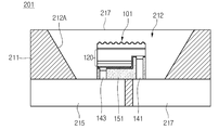
도 1은 제1실시 예에 따른 발광소자를 나타낸 측 단면도이며, 도 2는 도 1의 발광 소자의 저면도의 예를 나타낸 도면이다.FIG. 1 is a side sectional view showing a light emitting device according to a first embodiment, and FIG. 2 is a view showing an example of a bottom view of the light emitting device of FIG.
도 1 및 도 2를 참조하면, 발광 소자(100)는 기판(111), 제1반도체층(113), 제1도전형 반도체층(115), 활성층(117), 제2도전형 반도체층(119), 반사 전극층(131), 절연층(133), 제1전극(135), 제2전극(137), 제1연결 전극(141), 제2연결 전극(143), 및 지지부재(151)을 포함한다.1 and 2, a
상기 기판(111)은 투광성이 있는 절연성 또는 도전성 기판을 이용할 수 있으며, 예컨대, 사파이어(Al2O3), SiC, Si, GaAs, GaN, ZnO, Si, GaP, InP, Ge, Ga2O3 중 적어도 하나를 이용할 수 있다. 상기 기판(111)의 하면에는 상기 기판(111)과 상기 제1반도체층(113) 사이에 요철 패턴과 같은 광 추출 구조가 형성될 수 있으며, 상기의 요철 패턴은 상기 기판(111)의 식각을 통해 형성하거나, 별도의 러프니스와 같은 패턴을 형성할 수 있다. 상기 요철 패턴은 스트라이프 형상 또는 볼록 렌즈 형상을 포함할 수 있다.The
상기 기판(111)의 상면(S1)에는 복수의 돌기를 갖는 제1요철 구조의 제1패턴부(11)와, 상기 제1요철 구조 상에 복수의 오목부를 갖는 제2요철 구조의 제2패턴부(12)를 포함한다. 상기 제2요철 구조는 상기 제1요철 구조 상에 상기 돌기의 사이즈보다 작은 사이즈를 갖는 미세 요철로 형성될 수 있다.A
상기 제1패턴부(11)의 돌기는 상기 기판(111)의 상면(S1)으로부터 돌출되는 형상 또는 양각 형상으로 형성될 수 있다. 다른 예로서, 상기 제1패턴부(11)는 상기 기판(111)의 상면(S1)보다 낮은 깊이로 오목한 형상 또는 음각 형상의 오목부로 형성될 수 있다. 상기 제2패턴부(12)의 오목부는 상기 돌기의 표면과 상기 기판(111)의 상면(S1)에 상기 돌기의 사이즈보다 작은 사이즈로 음각 형상 또는 오목한 형상으로 형성될 수 있다. 다른 예로서, 상기 제2패턴부(12)는 양각 형상 또는 볼록한 형상을 갖고 상기 돌기의 사이즈보다 작은 사이즈의 미세 돌기로 형성될 수 있다.The projection of the
상기 제1패턴부(11)는 양각 형상의 돌기와 음각 형상을 갖는 평탄한 상면을 갖는 요철 구조를 포함하며, 상기 제2패턴부(12)는 상기 제1요철 구조 상에 상기 돌기의 너비보다 작은 너비를 갖고 음각 형상 및 양각 형상으로 형성된 미세 요철을 포함한다.The
상기 제1패턴부(11)의 배열 형상은 매트릭스 형태 또는 격자 형태로 형성될 수 있다. The arrangement pattern of the
제1실시 예는 설명의 편의를 위해, 상기 제1패턴부(11)는 돌기로 설명하며, 상기 제2패턴부(12)는 오목한 구조를 갖는 오목부로 설명하기로 하며, 이에 대해 한정하지는 않는다.For the sake of convenience, the
상기 기판(111)의 하면에는 제1반도체층(113)이 형성되며, 상기 하면의 반대측 상면(S1)에는 상기 기판(111)의 상면(S1)보다 상 방향으로 돌출된 복수의 돌기 및 상기 복수의 돌기에 형성된 오목부를 포함한다. 상기 복수의 돌기는 상기 상 방향의 단면이 반구형상, 원뿔 형상, 다각뿔 형상, 원 기둥 또는 다각 기둥과 같은 기둥 형상, 또는 뿔 대 형상과 같은 형상으로 형성될 수 있다. 상기 각 돌기는 위에서 볼 때, 원 형상, 다각형 형상, 구면과 각면이 혼합된 형상을 포함할 수 있다. A
상기 오목부는 상기 각 돌기의 표면보다 오목한 형상으로 형성될 수 있으며, 그 측 단면이 반구형상, 원뿔 형상, 다각뿔 형상, 원 기둥 또는 다각 기둥과 같은 기둥 형상, 또는 뿔 대 형상과 같은 형상으로 형성될 수 있다. 상기 각 오목부는 위에서 볼 때, 원 형상, 다각형 형상, 구면과 각면이 혼합된 형상을 포함할 수 있다. 상기 오목부는 상기 기판(111)의 상면(S1)으로부터 상기 기판(111)의 상면보다 더 오목하게 형성될 수 있다. 상기 오목부의 최대 너비는 상기 돌기의 최대 너비보다 작게 형성될 수 있다.The concave portion may be formed in a concave shape than the surface of each of the protrusions. The concave portion may be formed in a shape such as a hemispherical shape, a conical shape, a polygonal pyramid, a columnar shape such as a circular column or a polygonal column, . Each of the recesses may include a circular shape, a polygonal shape, and a shape in which spherical and angular surfaces are mixed when viewed from above. The concave portion may be formed to be more concave than the upper surface of the
상기 오목부의 사이즈 또는 상기 미세 요철의 사이즈는 상기 돌기의 사이즈에 비해 50% 이상 작은 사이즈로 형성될 수 있으며, 예컨대 상기 돌기의 사이즈에 비해 1/2~1/100 범위의 사이즈로 형성될 수 있다. 상기 돌기의 사이즈(B1)는 돌기의 최대 너비, 한 변의 길이, 반지름, 두께 또는 높이(L2) 중 적어도 하나일 수 있으며, 상기 오목부의 사이즈는 상기 오목부의 최대 너비, 각 변의 길이, 높이 또는 깊이, 반지름, 또는 두께 중 적어도 하나일 수 있다.The size of the concave portion or the size of the fine concavities and convexities may be smaller than 50% of the size of the protrusions, and may be in the range of 1/2 to 1/100 of the size of the protrusions . The size B1 of the protrusion may be at least one of a maximum width of the protrusion, a length of one side, a radius, a thickness, or a height L2. The size of the recess may be a maximum width of the recess, , Radius, or thickness.
상기 돌기의 너비(B1)의 사이즈 또는 두께(L1)의 사이즈는 0.1㎛-10㎛ 범위로 형성될 수 있으며, 예컨대 상기 기판(111)의 두께보다 작은 사이즈로 형성될 수 있다. 여기서, 상기 돌기의 너비는 상기 돌기의 두께(L1) 또는 높이보다 클 수 있으며, 이에 대해 한정하지는 않는다. 상기 오목부의 깊이 또는 너비의 사이즈는 0.1nm-100nm 범위로 형성되거나, 0.1nm-100㎛ 범위로 형성될 수 있다. 상기 돌기 간의 주기(L1)는 0.1㎛-100㎛ 범위로 형성될 수 있으며, 상기 오목부 간의 주기는 0.1㎛-100㎛ 범위로 형성될 수 있다.The size or the thickness L1 of the width B1 of the protrusion may be in the range of 0.1 mu m to 10 mu m and may be smaller than the thickness of the
상기 돌기는 입사되는 광의 임계각을 변환시켜 주며, 상기 오목부는 상기 돌기로 입사되는 광과 상기 기판(111) 상면(S1)으로 입사되는 광의 임계각을 변환시켜 주게 된다. 상기 기판(111)의 상부에 서로 다른 제1패턴부(11)와 제2패턴부(12)를 형성해 줌으로써, 입사되는 광의 전반사 비율을 낮추어 광 추출 효율을 개선시켜 줄 수 있다. The projection converts the critical angle of incident light, and the recess transforms the critical angle of light incident on the projection and light incident on the upper surface S1 of the
상기 돌기들은 일정한 주기로 형성되거나, 랜덤한 간격으로 형성될 수 있으며, 상기 오목부들은 일정한 주기로 형성되거나, 랜덤한 간격으로 형성될 수 있다.
The protrusions may be formed at regular intervals or may be formed at random intervals, and the recesses may be formed at regular intervals or at random intervals.
상기 기판(111) 하면에는 제1반도체층(113)이 형성될 수 있다. 상기 제1반도체층(113)은 II족 내지 VI족 화합물 반도체를 이용하여 형성될 수 있다. 상기 제1반도체층(113)은 II족 내지 VI족 화합물 반도체를 이용하여 적어도 한 층 또는 복수의 층으로 형성될 수 있다. 상기 제1반도체층(113)은 예컨대, III족-V족 화합물 반도체를 이용한 반도체층 예컨대, GaN, InN, AlN, InGaN, AlGaN, InAlGaN, AlInN 중 적어도 하나를 포함할 수 있다. 상기 제1반도체층(113)은 ZnO 층과 같은 산화물로 형성될 수 있으며, 이에 대해 한정하지는 않는다. A
상기 제1반도체층(113)은 버퍼층으로 형성될 수 있으며, 상기 버퍼층은 상기 기판과 질화물 반도체층 간의 격자 상수의 차이를 줄여줄 수 있다. The
상기 제1반도체층(113)은 언도프드(undoped) 반도체층으로 형성될 수 있다. 상기 언도프드 반도체층은 III족-V족 화합물 반도체 예컨대, GaN계 반도체로 구현될 수 있다. 상기 언도프드 반도체층은 제조 공정시 의도적으로 도전형 도펀트를 도핑하지 않더라도 제1도전형 특성을 가지게 되며, 상기 제1도전형 반도체층(115)의 도전형 도펀트 농도보다는 낮은 농도를 가지게 된다. The
상기 제1반도체층(113)은 버퍼층 및 언도프드 반도체층 중 적어도 하나로 형성될 수 있으며, 이에 대해 한정하지는 않는다.
The
상기 제1반도체층(113) 위에는 발광 구조물(120)이 형성될 수 있다. 상기 발광 구조물(120)은 III족-V족 화합물 반도체를 포함하며, 예컨대 InxAlyGa1-x-yN (0≤x≤1, 0≤y≤1, 0≤x+y≤1)의 조성식을 갖는 반도체를 갖고, 자외선 대역부터 가시 광선 대역의 파장 범위 내에서 소정의 피크 파장을 발광할 수 있다. The
상기 발광 구조물(120)은 제1도전형 반도체층(115), 제2도전형 반도체층(119), 상기 제1도전형 반도체층(115)과 상기 제2도전형 반도체층(119) 사이에 형성된 활성층(117)을 포함한다.The
상기 제1반도체층(113) 아래에는 제1도전형 반도체층(115)이 형성될 수 있다. 상기 제1도전형 반도체층(115)은 제1도전형 도펀트가 도핑된 III족-V족 화합물 반도체로 구현되며, 상기 제1도전형 반도체층(115)은 N형 반도체층이며, 상기 제1도전형 도펀트는 N형 도펀트로서, Si, Ge, Sn, Se, Te를 포함한다. A first
상기 제1도전형 반도체층(115)과 상기 제1반도체층(113) 사이에는 서로 다른 반도체층들이 교대로 적층된 초 격자 구조가 형성될 수 있으며, 이러한 초격자 구조는 격자 결함을 감소시켜 줄 수 있다. 상기 초 격자 구조의 각 층은 수 Å 이상의 두께로 적층될 수 있다. A superlattice structure in which different semiconductor layers are alternately stacked may be formed between the first conductive
상기 제1도전형 반도체층(115)과 상기 활성층(117) 사이에는 제1도전형 클래드층이 형성될 수 있다. 상기 제1도전형 클래드층은 GaN계 반도체로 형성될 수 있으며, 그 밴드 갭은 상기 활성층(117)의 밴드 갭 이상으로 형성될 수 있다. 이러한 제1도전형 클래드층은 캐리어를 구속시켜 주는 역할을 한다. A first conductive clad layer may be formed between the first
상기 제1도전형 반도체층(115) 아래에는 활성층(117)이 형성된다. 상기 활성층(117)은 단일 양자 우물, 다중 양자 우물(MQW), 양자 선(quantum wire) 구조 또는 양자 점(quantum dot) 구조를 선택적으로 포함하며, 우물층과 장벽층의 주기를 포함한다. 상기 우물층은 InxAlyGa1 -x- yN (0≤x≤1, 0≤y≤1, 0≤x+y≤1)의 조성식을 포함하며, 상기 장벽층은 InxAlyGa1-x-yN (0≤x≤1, 0≤y≤1, 0≤x+y≤1)의 조성식을 포함할 수 있다.An
상기 우물층/장벽층의 주기는 예컨대, InGaN/GaN, AlGaN/GaN, InGaN/AlGaN, InGaN/InGaN의 적층 구조를 이용하여 1주기 이상으로 형성될 수 있다. 상기 장벽층은 상기 우물층의 밴드 갭보다 넓은 밴드 갭을 가지는 반도체 물질로 형성될 수 있다. The period of the well layer / barrier layer may be formed in one cycle or more using a laminated structure of InGaN / GaN, AlGaN / GaN, InGaN / AlGaN, and InGaN / InGaN, for example. The barrier layer may be formed of a semiconductor material having a band gap wider than a band gap of the well layer.
상기 활성층(117) 아래에는 제2도전형 반도체층(119)이 형성된다. 상기 제2도전형 반도체층(119)은 제2도전형 도펀트가 도핑된 반도체 예컨대, GaN, InN, AlN, InGaN, AlGaN, InAlGaN, AlInN와 같은 화합물 반도체 중 어느 하나로 이루어질 수 있다. 상기 제2도전형 반도체층(119)이 P형 반도체층이고, 상기 제2도전형 도펀트는 P형 도펀트로서, Mg, Zn, Ca, Sr, Ba을 포함할 수 있다. A second
상기 제2도전형 반도체층(119)은 초격자 구조를 포함할 수 있으며, 상기 초격자 구조는 InGaN/GaN 초격자 구조 또는 AlGaN/GaN 초격자 구조를 포함할 수 있다. 상기 제2도전형 반도체층(119)의 초격자 구조는 비 정상적으로 전압에 포함된 전류를 확산시켜 주어, 활성층(117)을 보호할 수 있다.
The second
또한 상기 제1도전형 반도체층(115)은 P형 반도체층, 상기 제2도전형 반도체층(119)은 N형 반도체층으로 구현될 수 있다. 상기 제2도전형 반도체층(119) 위에는 상기 제2도전형과 반대의 극성을 갖는 제3도전형 반도체층이 형성할 수도 있다. The first
상기 발광소자(100)는 상기 제1도전형 반도체층(115), 활성층(117) 및 상기 제2도전형 반도체층(119)을 발광 구조물(120)로 정의될 수 있으며, 상기 발광 구조물은 N-P 접합 구조, P-N 접합 구조, N-P-N 접합 구조, P-N-P 접합 구조 중 어느 한 구조로 구현할 수 있다. 여기서, 상기 P는 P형 반도체층이며, 상기 N은 N형 반도체층이며, 상기 -은 P형 반도체층과 N형 반도체층이 직접 접촉되거나 간접 접촉된 구조를 포함한다. 이하, 설명의 편의를 위해, 발광 구조물(120)의 최 상층은 제2도전형 반도체층(119)으로 설명하기로 한다.
The
상기 제2도전형 반도체층(119) 아래에는 반사 전극층(131)이 형성된다. 상기 반사 전극층(131)은 오믹 접촉층, 반사층, 및 확산 방지층, 보호층 중 적어도 하나를 포함한다. A
상기 반사 전극층(131)은 오믹 접촉층/반사층/확산 방지층/보호층의 구조로 형성되거나, 반사층/확산 방지층/보호층의 구조로 형성되거나, 오믹 접촉층/반사층/보호층의 구조로 형성되거나, 반사층/확산 방지층으로 형성되거나, 반사층으로 형성될 수 있다.
The
여기서, 상기 오믹 접촉층은 상기 제2도전형 반도체층(119) 아래에 접촉되며, 그 접촉 면적은 상기 제2도전형 반도체층(119)의 하면 면적의 70% 이상으로 형성될 수 있다. 상기 오믹 접촉층은 ITO(indium tin oxide), IZO(indium zinc oxide), IZTO(indium zinc tin oxide), IAZO(indium aluminum zinc oxide), IGZO(indium gallium zinc oxide), IGTO(indium gallium tin oxide), AZO(aluminum zinc oxide), ATO(antimony tin oxide), GZO(gallium zinc oxide), SnO, InO, INZnO, ZnO, IrOx, RuOx, NiO, Ni, Cr 및 이들의 선택적인 화합물 또는 합금 중에서 선택되며, 적어도 한 층으로 형성될 수 있다. 상기 오믹 접촉층의 두께는 1~1,000Å로 형성될 수 있다. Here, the ohmic contact layer is in contact with the second
상기 반사층은 상기 오믹 접촉층 아래에 반사율이 70% 이상인 물질 예컨대, Al, Ag, Ru, Pd, Rh, Pt, Ir의 금속과 상기의 금속 중 2 이상의 합금 중에서 선택될 수 있다. 상기 반사층의 금속은 상기 제2도전형 반도체층(119) 아래에 오믹 접촉될 수 있으며, 이 경우 상기 오믹 접촉층은 형성하지 않을 수 있다. 상기 반사층의 두께는 1~10,000Å으로 형성될 수 있다. The reflective layer may be selected from a material having a reflectance of 70% or more below the ohmic contact layer, for example, a metal of Al, Ag, Ru, Pd, Rh, Pt, or Ir and at least two of the metals. The metal of the reflective layer may be in ohmic contact with the second conductive
상기 확산 방지층은 Au, Cu, Hf, Ni, Mo, V, W, Rh, Ru, Pt, Pd, La, Ta, Ti 및 이들 중에서 2이상의 합금 중에서 선택될 수 있다. 상기 확산 방지층은 서로 다른 층의 경계에서 층간 확산을 방지하게 된다. 상기 확산 방지층의 두께는 1~10,000Å로 형성될 수 있다. The diffusion preventing layer may be selected from Au, Cu, Hf, Ni, Mo, V, W, Rh, Ru, Pt, Pd, La, Ta and Ti and alloys of two or more thereof. The diffusion barrier prevents interdiffusion at the boundaries of the different layers. The thickness of the diffusion preventing layer may be 1 to 10,000 angstroms.
상기 보호층은 Au, Cu, Hf, Ni, Mo, V, W, Rh, Ru, Pt, Pd, La, Ta, Ti 및 이들 중에서 2이상의 합금 중에서 선택될 수 있으며, 그 두께는 1~10,000Å로 형성될 수 있다.
The protective layer may be selected from Au, Cu, Hf, Ni, Mo, V, W, Rh, Ru, Pt, Pd, La, Ta, Ti and alloys of two or more thereof. As shown in FIG.
상기 반사 전극층(131)은 투광성 전극층/반사층의 적층 구조를 포함할 수 있으며, 상기 투광성 전극층은 ITO(indium tin oxide), IZO(indium zinc oxide), IZTO(indium zinc tin oxide), IAZO(indium aluminum zinc oxide), IGZO(indium gallium zinc oxide), IGTO(indium gallium tin oxide), AZO(aluminum zinc oxide), ATO(antimony tin oxide), GZO(gallium zinc oxide), SnO, InO, INZnO, ZnO, IrOx, RuOx의 그룹 중에서 선택될 수 있다. 상기 투광성 전극층의 아래에는 반사층이 형성될 수 있으며, 상기 반사층은 제1굴절률을 갖는 제1층과 제2굴절률을 갖는 제2층이 교대로 2페어 이상 적층된 구조를 포함하며, 상기 제1 및 제2굴절률은 서로 다르고, 상기 제1층과 제2층은 1.5~2.4 사이의 물질 예컨대, 전도성 또는 절연성 물질로 형성될 수 있으며, 이러한 구조는 DBR(distributed bragg reflection) 구조로 정의될 수 있다. The
상기 제2도전형 반도체층(119) 및 상기 반사 전극층(131) 중 적어도 한 층의 표면에는 러프니스와 같은 광 추출 구조가 형성될 수 있으며, 이러한 광 추출 구조는 입사되는 광의 임계각을 변화시켜 주어, 광 추출 효율을 개선시켜 줄 수 있다.
A light extracting structure such as a roughness may be formed on the surface of at least one of the second conductive
상기 제1도전형 반도체층(115)의 일부 영역(A1) 아래에는 제1전극(135)이 형성되며, 상기 반사 전극층(131)의 일부 아래에는 제2전극(137)이 형성될 수 있다. 상기 제1전극(135) 아래에는 제1연결 전극(141)이 형성되며, 상기 제2전극(137) 아래에는 제2연결 전극(143)이 형성된다.A
상기 제1전극(135)는 상기 제1도전형 반도체층(115)의 일부 영역(A1)에 전기적으로 연결된다. 상기 제1전극(135)은 전극 패드를 포함할 수 있으며, 이에 대해 한정하지는 않는다.The
상기 제1전극(135)는 상기 활성층(117) 및 제2도전형 반도체층(119)의 측면과 이격되며, 상기 제1도전형 반도체층(115)의 일부 영역(A1) 보다 작은 면적으로 형성될 수 있다. The
상기 제2전극(137)은 상기 반사 전극층(131)을 통해 상기 제2도전형 반도체층(119)과 물리적 또는/및 전기적으로 접촉될 수 있다. 상기 제2전극(137)은 전극 패드를 포함한다.
The
상기 제1전극(135) 및 제2전극(137)은 접착층, 반사층, 확산 방지층, 및 본딩층 중 적어도 하나를 포함한다. 상기 접착층은 상기 제1도전형 반도체층(115)의 일부 영역(A1) 아래에 오믹 접촉되며, Cr, Ti, Co, Ni, V, Hf 및 이들의 선택적인 합금으로 형성될 수 있으며, 그 두께는 1~1,000Å으로 형성될 수 있다. 상기 반사층은 상기 접착층 아래에 형성되며, 그 물질은 Ag, Al, Ru, Rh, Pt, Pd 및 이들의 선택적인 합금으로 형성될 수 있으며, 그 두께는 1~10,000Å로 형성될 수 있다. 상기 확산 방지층은 상기 반사층 아래에 형성되며, 그 물질은 Ni, Mo, W, Ru, Pt, Pd, La, Ta, Ti 및 이들의 선택적인 합금으로 형성될 수 있으며, 그 두께는 1~10,000Å을 포함한다. 상기 본딩층은 상기 제1연결 전극(141)과 본딩되는 층이며, 그 물질은 Al, Ru, Rh, Pt 및 이들의 선택적인 합금으로 형성될 수 있으며, 그 두께는 1~10,000Å로 형성될 수 있다.The
상기 제1전극(135)과 상기 제2전극(137)은 동일한 적층 구조이거나 다른 적층 구조로 형성될 수 있다. 상기 제2전극(137)의 적층 구조가 상기 제1전극(135)의 적층 구조보다 적을 수 있으며, 예컨대 상기 제1전극(135)은 접착층/반사층/확산 방지층/본딩층의 구조 또는 접착층/확산방지층/본딩층의 구조로 형성될 수 있으며, 상기 제2전극(137)은 접착층/반사층/확산 방지층/본딩층의 구조 또는 접착층/확산방지층/본딩층의 구조로 형성될 수 있다. The
상기 제2전극(137)의 상면 면적은 상기 반사전극층(131)의 하면 면적과 동일한 면적이거나, 상기 제2연결 전극(143)의 상면 면적보다 적어도 큰 면적일 수 있다.
The upper surface area of the
상기 제1전극(135) 및 상기 제2전극(137) 중 적어도 하나는 전극 패드로부터 분기된 암(arm) 또는 핑거(finger) 구조와 같은 전류 확산 패턴이 더 형성될 수 있다. 또한 상기 제1전극(135) 및 상기 제2전극(137)의 전극 패드는 하나 또는 복수로 형성될 수 있으며, 이에 대해 한정하지는 않는다.
At least one of the
상기 제1연결 전극(141) 및 상기 제2연결 전극(143)은 전원을 공급하는 리드(lead) 기능과 방열 경로를 제공하게 된다. 상기 제1연결 전극(141) 및 상기 제2연결 전극(143)은 기둥 형상일 수 있으며, 예컨대 구형, 원 기둥 또는 다각 기둥과 같은 형상이거나 랜덤한 형상을 포함할 수 있다. 여기서, 상기 다각 기둥은 등각이거나 등각이 아닐 수 있으며, 이에 대해 한정하지는 않는다. 상기 제1연결 전극(141) 및 상기 제2연결 전극(143)의 상면 또는 하면 형상은 원형, 다각형을 포함할 수 있으며, 이에 대해 한정하지는 않는다. 상기 제1연결 전극(141) 및 상기 제2연결 전극(143)의 하면은 상면과 다른 면적으로 형성될 수 있으며, 예컨대 상기 하면 면적은 상면 면적보다 더 크거나 작을 수 있다.The
상기 제1연결 전극(141) 및 상기 제2연결 전극(143) 중 적어도 하나는 상기 발광 구조물(120)의 하면 너비보다는 작게 형성될 수 있고, 상기 각 전극(135,137)의 하면 너비 또는 직경 보다는 크게 형성될 수 있다. At least one of the
상기 제1연결 전극(141) 및 상기 제2연결 전극(143)의 직경 또는 너비는 1㎛~100,000㎛로 형성될 수 있으며, 그 높이는 1㎛~100,000㎛로 형성될 수 있다. 여기서, 상기 제1연결 전극(141)의 두께(H1)는 상기 제2연결 전극(143)의 두께(H2)보다 더 길게 형성될 수 있으며, 상기 제1연결 전극(141) 및 상기 제2연결 전극(143)의 하면은 동일한 평면 (즉, 수평 면) 상에 배치될 수 있다.
The
상기 제1연결 전극(141) 및 제2연결 전극(143)은 어느 하나의 금속 또는 합금을 이용하여 단일 층으로 형성될 수 있으며, 상기의 단일 층의 너비 및 높이는 1㎛~100,000㎛로 형성될 수 있으며, 예컨대 상기 단일층 층의 두께는 상기 제2전극(143)의 두께보다 더 두꺼운 높이로 형성될 수 있다. The
상기 제1연결 전극(141) 및 제2연결 전극(143)은 Ag, Al, Au, Cr, Co, Cu, Fe, Hf, In, Mo, Ni, Si, Sn, Ta, Ti, W 및 이들 금속의 선택적 합금 중 어느 하나로 형성될 수 있다. 상기 제1연결 전극(141) 및 제2연결 전극(143)은 상기 제1전극(135) 및 제2전극(137)과의 접착력 향상을 위하여 In, Sn, Ni, Cu 및 이들의 선택적인 합금 중의 어느 한 금속으로 도금될 수 있다. 이때 도금두께는 1~100,000Å이 적용 가능하다.The
상기 제1연결 전극(141) 및 상기 제2연결 전극(143)의 표면에는 도금층이 더 형성될 수 있으며, 상기 도금층은 Tin 또는 이의 합금, Ni 또는 이의 합금, Tin-Ag-Cu 합금으로 형성될 수 있으며, 그 두께는 0.5㎛~10㎛로 형성될 수 있다. 이러한 도금층은 다른 본딩층과의 접합을 개선시켜 줄 수 있다.
A plating layer may further be formed on the surfaces of the
상기 절연층(133)은 상기 반사 전극층(131) 아래에 형성될 수 있다. 상기 절연층(133)은 상기 제2도전형 반도체층(119)의 하면, 상기 제2도전형 반도체층(119) 및 상기 활성층(117)의 측면, 상기 제1도전형 반도체층(115)의 일부 영역(A1)의 하면에 형성될 수 있다. 상기 절연층(133)은 상기 발광 구조물(120)의 하부 영역 중에서 상기 반사 전극층(131), 제1전극(135) 및 제2전극(137)을 제외한 영역에 형성되어, 상기 발광 구조물(120)의 하부를 전기적으로 보호하게 된다.The insulating
상기 절연층(133)은 Al, Cr, Si, Ti, Zn, Zr 중 적어도 하나를 갖는 산화물, 질화물, 불화물, 및 황화물 중 적어도 하나로 형성된 절연물질 또는 절연성 수지를 포함한다. 상기 절연층(133)은 예컨대, SiO2, Si3N4, Al2O3, TiO2 중에서 선택적으로 형성될 수 있다. 상기 절연층(133)은 단층 또는 다층으로 형성될 수 있으며, 이에 대해 한정하지는 않는다. 상기 절연층(133)은 발광 구조물(120)의 아래에 플립 본딩을 위한 금속 구조물을 형성할 때, 상기 발광 구조물(120)의 층간 쇼트를 방지하기 위해 형성된다.The insulating
상기 절연층(133)은 상기 반사 전극층(131) 하면에 형성되지 않고, 상기 발광 구조물(120)의 표면에만 형성될 수 있다. 이는 상기 반사 전극층(131)의 하면에는 절연성의 지지 부재(151)가 형성됨으로써, 상기 절연층(133)을 상기 반사 전극층(131)의 하면까지 연장하지 않을 수 있다.The insulating
상기 절연층(133)은 서로 다른 굴절률을 갖는 제1층과 제2층이 교대로 배치된 DBR 구조로 형성될 수 있으며, 상기 제1층은 SiO2, Si3N4, Al2O3, TiO2 중에서 어느 하나이며, 상기 제2층은 상기 제1층 이외의 물질 중 어느 하나로 형성될 수 있다. 이 경우, 상기 반사 전극층은 형성하지 않을 수 있다. The insulating
상기 절연층(133)은 100~10,000Å 두께로 형성되며, 다층 구조로 형성된 경우 각 층은 1~50,000Å의 두께이거나, 각 층당 100~10,000Å의 두께로 형성될 수 있다. 여기서, 상기 다층 구조의 절연층(133)에서 각 층의 두께는 발광 파장에 따라 반사 효율을 변화시켜 줄 수 있다.
The insulating
상기 제1연결 전극(141) 및 상기 제2연결 전극(143)의 재질은 Ag, Al, Au, Cr, Co, Cu, Fe, Hf, In, Mo, Ni, Si, Sn, Ta, Ti, W 및 이들의 선택적인 합금으로 형성될 수 있다. 또한 상기 제1연결 전극(141)과 상기 제2연결 전극(143)은 상기 제1전극(135)와 상기 제2전극(137)과의 접착력을 위해 In, Sn, Ni, Cu 및 이들의 합금을 이용한 도금층을 포함할 수 있으며, 상기 도금층의 두께는 1~100,000Å로 형성될 수 있다. 상기 제1연결 전극(141) 및 상기 제2 연결 전극(143)은 유테틱(eutectic) 본딩, 솔더 볼 또는 금속 범프로 본딩될 수 있으며, 이에 대해 한정하지는 않는다. The
상기 제1연결 전극(141) 및 상기 제2연결 전극(143)의 재질은 Ag, Al, Au, Cr, Co, Cu, Fe, Hf, In, Mo, Ni, Si, Sn, Ta, Ti, W 및 이들의 선택적인 합금으로 형성될 수 있다. 또한 상기 제1연결 전극(141)과 상기 제2연결 전극(143)은 상기 제1전극(135)와 상기 제2전극(137)과의 접착력을 위해 In, Sn, Ni, Cu 및 이들의 합금을 이용한 도금층을 포함할 수 있으며, 상기 도금층의 두께는 1~100,000Å로 형성될 수 있다. 상기 제1연결 전극(141) 및 상기 제2 연결 전극(143)은 솔더 볼 또는 금속 범프와 같은 단일 금속으로 사용될 수 있으며, 이에 대해 한정하지는 않는다.The
상기 지지 부재(151)는 발광 소자(100)를 지지하는 지지층으로 사용된다. 상기 지지 부재(151)는 절연성 재질로 형성되며, 상기 절연성 재질은 예컨대, 실리콘 또는 에폭시와 같은 수지층으로 형성된다. 다른 예로서, 상기 절연성 재질은 페이스트 또는 절연성 잉크를 포함할 수 있다. 상기 절연성 재질의 재질은 그 종류는 polyacrylate resin, epoxy resin, phenolic resin, polyamides resin, polyimides rein, unsaturated polyesters resin, polyphenylene ether resin (PPE), polyphenilene oxide resin (PPO), polyphenylenesulfides resin, cyanate ester resin, benzocyclobutene (BCB), Polyamido-amine Dendrimers (PAMAM), 및 Polypropylene-imine, Dendrimers (PPI), 및 PAMAM 내부 구조 및 유기-실리콘 외면을 갖는 PAMAM-OS(organosilicon)를 단독 또는 이들의 조합을 포함한 수지로 구성될 수 있다. 상기 지지부재(151)은 상기 절연층(133)과 다른 물질로 형성될 수 있다.The
상기 지지 부재(151) 내에는 Al, Cr, Si, Ti, Zn, Zr 중 적어도 하나를 갖는 산화물, 질화물, 불화물, 황화물과 같은 화합물들 중 적어도 하나가 첨가될 수 있다. 여기서, 상기 지지 부재(151) 내에 첨가된 화합물은 열 확산제일 수 있으며, 상기 열 확산제는 소정 크기의 분말 입자, 알갱이, 필러(filler), 첨가제로 사용될 수 있으며, 이하 설명의 편의를 위해 열 확산제로 설명하기로 한다. 여기서, 상기 열 확산제는 절연성 재질 또는 전도성 재질일 수 있으며, 그 크기는 1Å~100,000Å으로 사용 가능하며, 열 확산 효율을 위해 1,000Å~50,000Å로 형성될 수 있다. 상기 열 확산제의 입자 형상은 구형 또는 불규칙한 형상을 포함할 수 있으며, 이에 대해 한정하지는 않는다. At least one of compounds such as oxides, nitrides, fluorides and sulfides having at least one of Al, Cr, Si, Ti, Zn and Zr may be added to the
상기 열 확산제는 세라믹 재질을 포함하며, 상기 세라믹 재질은 동시 소성되는 저온 소성 세라믹(LTCC: low temperature co-fired ceramic), 고온 소성 세라믹(HTCC: high temperature co-fired ceramic), 알루미나(alumina), 수정(quartz), 칼슘지르코네이트(calcium zirconate), 감람석(forsterite), SiC, 흑연, 용융실리카(fusedsilica), 뮬라이트(mullite), 근청석(cordierite), 지르코니아(zirconia), 베릴리아(beryllia), 및 질화알루미늄(aluminum nitride) 중 적어도 하나를 포함한다. 상기 세라믹 재질은 질화물 또는 산화물과 같은 절연성 물질 중에서 열 전도도가 질화물이나 산화물보다 높은 금속 질화물로 형성될 수 있으며, 상기 금속 질화물은 예컨대, 열 전도도가 140 W/mK 이상의 물질을 포함할 수 있다. 상기 세라믹 재질은 예컨대, SiO2, SixOy, Si3N4, SixNy, SiOxNy, Al2O3, BN, Si3N4, SiC(SiC-BeO), BeO, CeO, AlN와 같은 세라믹 (Ceramic) 계열일 수 있다. 상기 열 전도성 물질은 C (다이아몬드, CNT)의 성분을 포함할 수 있다. The heat spreader may include a ceramic material. The ceramic material may include a low temperature co-fired ceramic (LTCC), a high temperature co-fired ceramic (HTCC), an alumina, Quartz, calcium zirconate, forsterite, SiC, graphite, fused silica, mullite, cordierite, zirconia, beryllia, ), And aluminum nitride. The ceramic material may be formed of a metal nitride having thermal conductivity higher than that of nitride or oxide among the insulating materials such as nitride or oxide, and the metal nitride may include a material having a thermal conductivity of, for example, 140 W / mK or more. The ceramic material may be, for example, SiO 2 , Si x O y , Si 3 N 4 , Si x N y , SiO x N y , Al 2 O 3 , BN, Si 3 N 4 , SiC (SiC- CeO 2, AlN, and the like. The thermally conductive material may comprise a component of C (diamond, CNT).
상기 지지 부재(151)는 단층 또는 다층으로 형성될 수 있으며, 이에 대해 한정하지는 않는다. 상기 지지 부재(151)는 내부에 세라믹 물질의 분말을 포함함으로써, 지지 부재(151)의 강도는 개선되고, 열 전도율 또한 개선될 수 있다.
The
상기 지지 부재(151) 내에 포함된 열 확산제는 1~99wt/% 정도의 함량 비율로 첨가될 수 있으며, 효율적인 열 확산을 위해 50~99wt% 범위의 함량 비율로 첨가될 수 있다. 이러한 지지 부재(151) 내에 열 확산제가 첨가됨으로써, 내부에서의 열 전도율은 더 개선될 수 있다. 또한 상기 지지 부재(151)의 열 팽창 계수는 4-11 [x106/℃]이며, 이러한 열 팽창 계수는 상기 기판(111) 예컨대, 사파이어 기판과 동일하거나 유사한 열 팽창 계수를 갖게 되므로, 상기 기판(111) 아래에 형성되는 발광 구조물(120)과의 열 팽창 차이에 의해 웨이퍼가 휘어지거나 결함이 발생되는 것을 억제하여 발광 소자의 신뢰성이 저하되는 것을 방지할 수 있다.The heat diffusion agent contained in the
여기서, 상기 지지 부재(151)의 하면 면적은 상기 기판(111)의 상면과 실질적으로 동일한 면적으로 형성될 수 있다. 상기 지지 부재(151)의 하면 면적은 상기 제1도전형 반도체층(115)의 상면 면적과 실질적으로 동일한 면적으로 형성될 수 있다. 또한 상기 지지 부재(151)의 하면 너비는 상기 기판(111)의 상면과 상기 제1도전형 반도체층(115)의 상면 너비와 동일한 너비로 형성될 수 있다. 이는 지지 부재(151)를 형성한 다음 개별 칩으로 분리함으로써, 상기 지지부재(151)과 상기 기판(111) 및 상기 제1도전형 반도체층(115)의 측면이 동일 평면 상에 배치될 수 있다. 다른 예로서, 상기 지지 부재(151)의 하면 면적은 상기 기판(111)의 상면(S1) 면적보다 더 넓거나 더 좁을 수 있으며, 이에 대해 한정하지는 않는다.
Here, the lower surface area of the
도 2를 참조하면, 상기 지지 부재(151)의 제1변(D1)의 길이는 상기 지지부재(151)의 제1변(D1)에 대응되는 상기 기판(111)의 제1변의 길이와 실질적으로 동일하고, 제2변(D2)의 길이는 상기 지지부재(151)의 제2변(D2)에 대응되는 상기 기판(111)의 제2변의 길이와 실질적으로 동일하게 형성될 수 있다. 다른 예로서, 상기 지지 부재(151)의 각 변(D1,D2)의 길이는 상기 기판(111)의 각 변보다 길거나 작을 수 있으며, 이에 대해 한정하지는 않는다. 또한 제1연결 전극(141)과 제2연결 전극(143) 사이의 간격(D5)은 각 전극 패드 사이의 간격으로서, 발광 소자의 한 변의 길이의 1/2 이상 이격될 수 있다.2, the length of the first side D1 of the
상기 지지 부재(151)의 하면은 실질적으로 평탄한 면으로 형성되거나, 불규칙한 면으로 형성될 수 있으며, 이에 대해 한정하지는 않는다.The lower surface of the
상기 지지 부재(151)의 제1영역의 두께(T1)는 상기 제2연결 전극(143)의 두께(H2)보다 적어도 두껍게 형성될 수 있다. 다른 예로서, 상기 지지 부재(151)의 제1영역의 두께(T1)는 상기 제2연결 전극(143)의 두께(H2)보다 얇게 형성될 수 있으며, 이는 상기 절연층(133)의 두께를 상기 제2전극(137)의 두께보다 더 두껍게 형성함으로써, 상기 지지 부재(151)의 두께가 얇아질 수 있다. 상기 지지 부재(151)의 제2영역의 두께(T2)는 상기 제1연결 전극(141)의 두께보다 더 두껍게 형성될 수 있다. 상기 지지 부재(151)의 두께(T1)은 1㎛~100,000㎛ 범위에서 형성될 수 있으며, 다른 예로서 50㎛~1,000㎛ 범위로 형성될 수 있다.The thickness T1 of the first region of the
상기 지지 부재(151)의 하면은 상기 제1전극(135) 및 상기 제2전극(137)의 하면보다 더 낮게 형성되고, 상기 제1연결 전극(141)의 하면, 상기 제2연결 전극(143)의 하면과 동일한 평면(즉, 수평 면) 상에 배치될 수 있다.The lower surface of the
상기 지지 부재(151)는 상기 제1전극(135), 제2전극(137), 상기 제1연결 전극(141) 및 상기 제2연결 전극(143)의 둘레 면에 접촉된다. 이에 따라 상기 제1전극(135), 제2전극(137), 상기 제1연결 전극(141) 및 상기 제2연결 전극(143)으로부터 전도된 열은 상기 지지 부재(151)를 통해 확산되고 방열될 수 있다. 이때 상기 지지 부재(151)는 내부의 열 확산제에 의해 열 전도율이 개선되고, 전 표면을 통해 방열을 수행하게 된다. 따라서, 상기 발광 소자(100)는 열에 의한 신뢰성을 개선시켜 줄 수 있다.The
또한 상기 지지 부재(151)의 한 측면 또는 한 측면 이상은 상기 발광 구조물(120) 및 상기 기판(111)의 측면과 동일한 평면 (즉, 수직 면) 상에 배치될 수 있다. 또한 상기 지지 부재(151)의 한 측면 또는 한 측면 이상은 상기 발광 구조물(120) 및 상기 기판(111)의 측면보다 더 돌출될 수 있으며, 이에 대해 한정하지는 않는다. In addition, one side or one side or more of the
상기의 발광 소자(100)는 플립 방식으로 탑재되며, 기판(111)의 상면 방향으로 대부분의 광이 방출되고, 일부 광은 상기 기판(111)의 측면 및 상기 발광 구조물(120)의 측면을 통해 방출되기 때문에, 상기 제1전극(135) 및 제2전극(137)에 의한 광 손실을 줄여줄 수 있다. 이에 따라 상기의 발광 소자(100)의 상부에 배치된 상기 기판(111)의 서로 다른 사이즈를 갖는 제1패턴부(11)와 제2패턴부(12)에 의해 광 추출 효율이 개선되고, 상기 지지부재(151)에 의해 방열 효율은 개선될 수 있다.
Most of the light is emitted in the direction of the top surface of the
도 3 내지 도 9는 제1실시 예에 따른 발광 소자의 제조 과정을 나타낸 도면이다. 이하의 제조 과정은 설명의 용이성을 위해 개별 소자로 도시되었으나, 웨이퍼 레벨에서 제조되며, 개별 소자는 후술하는 처리 공정을 통해 제조되는 것으로 설명될 수 있다. 또한 개별 소자의 후술하는 제조 공정으로 한정하는 것이 아니며, 각 공정의 특정 공정에 추가적인 공정 또는 더 적은 공정으로 제조될 수 있다. 3 to 9 are views illustrating a manufacturing process of the light emitting device according to the first embodiment. Although the following manufacturing processes are shown as individual elements for ease of explanation, they are manufactured at the wafer level, and individual elements can be described as being manufactured through a processing process described below. Further, the present invention is not limited to the production process of the individual elements described below, and can be manufactured in an additional process or a fewer process in a specific process of each process.
도 3을 참조하면, 기판(111)은 성장 장비에 로딩되고, 그 위에 2족 내지 6족 원소의 화합물 반도체가 층 또는 패턴 형태로 형성될 수 있다. 상기 기판(111)은 성장 기판으로 사용된다.Referring to FIG. 3, the
여기서, 상기 기판(111)은 투광성 기판, 절연 기판 또는 전도성 기판으로 이루어질 수 있으며, 예컨대, 사파이어 기판(Al2O3), GaN, SiC, ZnO, Si, GaP, InP, Ga2O3, 그리고 GaAs 등으로 이루어진 군에서 선택될 수 있다. 이러한 기판(111)의 상면에는 요철 패턴과 같은 광 추출 구조가 형성될 수 있으며, 이러한 요철 패턴은 광의 임계각을 변화시켜 주어 광 추출 효율을 개선시켜 줄 수 있다.The
상기 성장 장비는 전자빔 증착기, PVD(physical vapor deposition), CVD(chemical vapor deposition), PLD(plasma laser deposition), 이중형의 열증착기(dual-type thermal evaporator), 스퍼터링(sputtering), MOCVD(metal organic chemical vapor deposition) 등에 의해 형성할 수 있으며, 이러한 장비로 한정하지는 않는다. The growth equipment may be an electron beam evaporator, physical vapor deposition (PVD), chemical vapor deposition (CVD), plasma laser deposition (PLD), dual-type thermal evaporator, sputtering, MOCVD vapor deposition, and the like, and the present invention is not limited thereto.
상기 기판(111) 위에는 제1반도체층(113)이 형성되며, 상기 제1반도체층(113)은 III족-V족 원소의 화합물 반도체를 이용하여 형성될 수 있다. 상기 제1반도체층(113)은 상기 기판(111)과의 격자 상수의 차이를 줄여주는 버퍼층으로 형성될 수 있다. 상기 제1반도체층(113)은 언도프드 반도체층으로 형성될 수 있으며, 상기 언도프드 반도체층은 의도적으로 도핑하지 않는 GaN계 반도체로 형성될 수 있다. A
상기 제1반도체층(113) 위에는 발광 구조물(120)이 형성될 수 있다. 상기 발광 구조물(120)은 제1도전형 반도체층(115), 활성층(117) 및 제2도전형 반도체층(119)의 순서로 형성될 수 있다.The
상기 제1도전형 반도체층(115)은 제1도전형 도펀트가 도핑된 III족-V족 원소의 화합물 반도체 예컨대, GaN, AlN, AlGaN, InGaN, InN, InAlGaN, AlInN, AlGaAs, GaP, GaAs, GaAsP, AlGaInP 등에서 선택될 수 있다. 상기 제1도전형이 N형 반도체인 경우, 상기 제1도전형 도펀트는 Si, Ge, Sn, Se, Te 등과 같은 N형 도펀트를 포함한다. 상기 제1도전형 반도체층(115)은 단층 또는 다층으로 형성될 수 있으며, 이에 대해 한정하지는 않는다. 상기 제1도전형 반도체층(115)은 서로 다른 물질을 갖는 초격자 구조를 더 포함할 수 있으며, 이에 대해 한정하지는 않는다. The first
상기 제1도전형 반도체층(115) 위에는 활성층(117)이 형성되며, 상기 활성층(117)은 단일 양자 우물 구조, 다중 양자 우물 구조, 양자 선 구조, 양자 점 구조 중 적어도 하나를 포함할 수 있다. 상기 활성층(117)은 III족-V족 원소의 화합물 반도체 재료를 이용하여 InxAlyGa1 -x- yN (0≤x≤1, 0≤y≤1, 0≤x+y≤1)의 조성식을 갖는 우물층과 장벽층의 주기, 예를 들면 InGaN 우물층/GaN 장벽층의 주기, InGaN 우물층/AlGaN 장벽층의 주기, InGaN우물층/InGaN 장벽층의 주기 등으로 형성될 수 있으며, 이에 대해 한정하지는 않는다. An
상기 활성층(117)의 위 또는/및 아래에는 도전형 클래드층이 형성될 수 있으며, 상기 도전형 클래드층은 AlGaN계 반도체로 형성될 수 있다. 여기서, 상기 활성층(117)의 장벽층은 상기 우물층의 밴드 갭보다 넓고, 상기 도전형 클래드층은 상기 장벽층의 밴드 갭보다 넓게 형성될 수 있다.A conductive clad layer may be formed on and / or below the
상기 활성층(117) 위에는 상기 제2도전형 반도체층(119)이 형성되며, 상기 제 2도전형 반도체층(119)은 제2도전형 도펀트가 도핑된 III족-V족 원소의 화합물 반도체 예컨대, GaN, AlN, AlGaN, InGaN, InN, InAlGaN, AlInN, AlGaAs, GaP, GaAs, GaAsP, AlGaInP 등에서 선택될 수 있다. 상기 제2도전형이 P형 반도체인 경우, 상기 제2도전형 도펀트는 Mg, Zn 등과 같은 P형 도펀트를 포함한다. 상기 제2도전형 반도체층(119)은 단층 또는 다층으로 형성될 수 있고, 이에 대해 한정하지는 않는다. 상기 제2도전형 반도체층(119)은 서로 다른 물질을 갖는 초격자 구조를 더 포함할 수 있으며, 이에 대해 한정하지는 않는다.The second conductivity
상기 제1도전형 반도체층(115), 상기 활성층(117) 및 상기 제2도전형 반도체층(119)은 발광 구조물(120)로 정의될 수 있다. 또한 상기 제2도전형 반도체층(119) 위에는 제2도전형과 반대의 극성을 갖는 제3도전형 반도체층 예컨대, N형 반도체층이 형성될 수 있다. 이에 따라 상기 발광 구조물(120)은 N-P 접합, P-N 접합, N-P-N 접합, P-N-P 접합 구조 중 적어도 하나로 형성될 수 있다.
The first
도 4를 참조하면, 발광 구조물(120)의 일부 영역(A1)에 대해 에칭을 수행하게 된다. 상기 발광 구조물(120)의 일부 영역(A1)은 상기 제1도전형 반도체층(115)이 노출될 수 있으며, 상기 제1도전형 반도체층(115)의 노출 부분은 상기 활성층(117)의 상면보다 낮은 높이로 형성될 수 있다.Referring to FIG. 4, etching is performed on a partial area A1 of the
상기 에칭 과정은 상기 발광 구조물(120)의 상면 영역에 대해 마스크 패턴으로 마스킹한 다음, 상기 발광 구조물(120)의 일부 영역(A1)에 대해 건식 에칭을 수행하게 된다. 상기 건식 에칭은 ICP(Inductively Coupled Plasma) 장비, RIE(Reactive Ion Etching) 장비, CCP(Capacitive Coupled Plasma) 장비, 및 ECR(Electron Cyclotron Resonance) 장비 중 적어도 하나를 포함한다. 다른 에칭 방식으로서, 습식 에칭을 더 포함할 수 있으며, 이에 대해 한정하지는 않는다. The etching process is performed by masking the upper surface region of the
여기서, 상기 발광 구조물(120)의 일부 영역(A1)은 에칭 영역으로서, 임의의 영역으로 설정될 수 있으며, 그 영역(A1)의 개수도 하나 또는 복수로 형성될 수 있다. Here, a part of the area A1 of the
도 5를 참조하면, 상기 발광 구조물(120) 위에 반사 전극층(131)을 형성하게 된다. 상기 반사 전극층(131)은 상기 제2도전형 반도체층(119)의 상면 면적보다 작은 면적으로 형성될 수 있으며, 이는 반사 전극층(131)의 제조 과정에 따른 쇼트를 방지할 수 있다. 여기서, 상기 반사 전극층(131)은 상기 제2도전형 반도체층(119)의 상면 에지로부터 소정 거리(D3) 이격된 영역과 상기 발광 구조물(120)의 일부 영역(A1)에 마스크로 마스킹한 다음, 스퍼터(Sputter) 장비 또는/및 증착 장비로 증착시켜 줄 수 있다. Referring to FIG. 5, a
상기 반사 전극층(131)은 적어도 반사율이 70% 이상이거나, 적어도 90% 이상인 금속 물질을 포함할 수 있다.The
상기 반사 전극층(131)은 오믹 접촉층/반사층/확산 방지층/보호층의 구조로 형성되거나, 반사층/확산 방지층/보호층의 구조로 형성되거나, 오믹 접촉층/반사층/보호층의 구조로 형성되거나, 반사층으로 형성될 수 있다. 상기 각 층의 물질 및 두께는 도 1의 설명을 참조하기로 한다.The
상기 제1도전형 반도체층(115) 위에 제1전극(135)를 형성하고, 상기 반사 전극층(131) 위에 제2전극(137)을 형성하게 된다. 상기 제1전극(135) 및 제2전극(137)은 전극 형성 영역 이외의 영역을 마스크로 마스킹한 다음, 스퍼터 또는/및 증착 장비로 형성될 수 있으며, 이에 대해 한정하지는 않는다. 상기 제1전극(135) 및 제2전극(137)은 Cr, Ti, Co, Ni, V, Hf, Ag, Al, Ru, Rh, Pt, Pd, Ni, Mo, W, La, Ta, Ti 및 이들의 선택적인 합금 중에서 선택적으로 형성될 수 있다. 상기 제1전극(135) 및 제2전극(137)은 다층으로 형성될 수 있으며, 예컨대 상기의 물질을 이용하여 접착층/반사층/확산방지층/본딩층 중 적어도 2층을 포함할 수 있다. 상기 제1전극(135)와 상기 제2전극(137)은 동일 공정으로 동일한 적층 구조로 형성될 수 있으며, 이에 대해 한정하지는 않는다. A
상기 제2전극(137)은 상기 반사 전극층(131)과 상기 제2도전형 반도체층(119)에 물리적으로 접촉될 수 있다.
The
상기 반사 전극층(131) 위에 절연층(133)을 형성하게 된다. 상기 절연층(133)은 스퍼터 또는 증착 방식으로 형성될 수 있다. 상기 절연층(133)은 상기 제1전극(135) 및 상기 제2전극(137)을 제외한 영역 상에 형성되어, 상기 반사 전극층(131) 및 상기 제2도전형 반도체층(119)의 상면, 상기 제1도전형 반도체층(115)의 노출된 영역을 커버하게 된다.An insulating
상기 절연층(133)은 Al, Cr, Si, Ti, Zn, Zr과 같은 물질의 산화물, 질화물, 불화물, 황화물 등 절연물질 또는 절연성 수지를 포함한다. 상기 절연층(133)은 예컨대, SiO2, Si3N4, Al2O3, TiO2 중에서 선택적으로 형성될 수 있다. 상기 절연층(133)은 단층 또는 다층으로 형성될 수 있으며, 이에 대해 한정하지는 않는다. The insulating
여기서, 전극(135,137)의 형성 과정과 절연층(133)의 형성 과정은 서로 변경될 수 있다.
Here, the process of forming the
도 6을 참조하면, 상기 제1전극(135) 위에 제1연결 전극(141)을 본딩하고, 상기 제2전극(137) 위에 제2연결 전극(143)을 본딩하게 된다. 상기 제1 연결 전극(141)는 솔더 볼 또는/및 금속 범프와 같은 전도성 패드를 포함하며, 상기 제1전극(135) 상에 본딩된다. 상기 제1연결 전극(141)은 상기 제1도전형 반도체층(115)의 상면에 대해 수직한 방향으로 배치될 수 있다. 상기 제2연결 전극(143)은 솔더 볼 또는/및 금속 범프와 같은 전도성 패드를 포함하며, 상기 제2전극(137) 상에 본딩된다. 상기 제2연결 전극(143)은 상기 제2도전형 반도체층(119)의 상면에 대해 수직한 방향으로 배치될 수 있다.Referring to FIG. 6, a
여기서, 상기 제1연결 전극(141)의 두께(H1)는 상기 제2연결 전극(143)의 두께(H2)보다 적어도 길게 형성될 수 있으며, 상기 제1연결 전극(141) 및 상기 제2연결 전극(143)의 하면은 서로 다른 평면 상에 배치되고, 이들의 상면은 동일한 평면 (즉, 수평 면)상에 배치된다.
The thickness H1 of the
도 7를 참조하면, 지지 부재(151)는 상기 절연층(133) 위에 스퀴지 또는/및 디스펜싱 방식으로 형성하게 된다. Referring to FIG. 7, the
상기 지지 부재(151)는 실리콘 또는 에폭시와 같은 수지물 내에 열 확산제를 첨가하여 절연성 지지층으로 형성된다. The
상기 열 확산제는 Al, Cr, Si, Ti, Zn, Zr과 같은 물질을 갖는 산화물, 질화물, 불화물, 황화물 중 적어도 하나의 물질 예컨대, 세라믹 재질을 포함할 수 있다. 상기 열 확산제는 소정 크기의 분말 입자, 알갱이, 필러(filler), 첨가제로 정의될 수 있다. The heat spreader may include at least one material selected from the group consisting of oxides, nitrides, fluorides, and sulfides having a material such as Al, Cr, Si, Ti, Zn, and Zr. The heat spreader may be defined as a powder particle, a grain, a filler, or an additive having a predetermined size.
상기 열 확산제는 세라믹 재질을 포함하며, 상기 세라믹 재질은 동시 소성되는 저온 소성 세라믹(LTCC: low temperature co-fired ceramic) 또는 고온 소성 세라믹(HTCC: high temperature co-fired ceramic)을 포함한다. 상기 세라믹 재질은 질화물 또는 산화물과 같은 절연성 물질 중에서 열 전도도가 질화물이나 산화물보다 높은 금속 질화물로 형성될 수 있으며, 상기 금속 질화물은 예컨대, 열 전도도가 140 W/mK 이상의 물질을 포함할 수 있다. 상기 세라믹 재질은 SiO2, SixOy, Si3N4, SixNy, SiOxNy, Al2O3, BN, Si3N4, SiC(SiC-BeO), BeO, CeO, AlN와 같은 세라믹 (Ceramic) 계열일 수 있다. 상기 열 전도성 물질은 C (다이아몬드, CNT)의 성분을 포함할 수 있다. 상기 열 확산제는 상기 지지 부재(151) 내에 1~99Wt/% 정도로 포함될 수 있어, 열 확산 효율을 위해 50% 이상으로 첨가될 수 있다.The heat spreader includes a ceramic material, and the ceramic material includes a low temperature co-fired ceramic (LTCC) or a high temperature co-fired ceramic (HTCC). The ceramic material may be formed of a metal nitride having thermal conductivity higher than that of nitride or oxide among the insulating materials such as nitride or oxide, and the metal nitride may include a material having a thermal conductivity of, for example, 140 W / mK or more. The ceramic material may be selected from the group consisting of SiO 2 , Si x O y , Si 3 N 4 , Si x N y , SiO x N y , Al 2 O 3 , BN, Si 3 N 4 , SiC (BeC) And may be a ceramic type such as AlN. The thermally conductive material may comprise a component of C (diamond, CNT). The heat spreader may be contained in the
상기 지지 부재(151)는 잉크 또는 페이스트에 고분자 물질을 혼합하여 형성될 수 있으며, 상기 고분자 물질의 혼합 방식은 볼밀, 유성 볼밀, 임펠라 믹싱, Bead Mill, Basket Mill 을 이용한다. 이 경우 고른 분산을 위하여 용매와 분산제가 사용될 수 있으며, 용매는 점도 조절을 위해 첨가되며, 잉크의 경우 3 ~ 400Cps, 페이스트의 경우 1000 ~ 1백만 Cps 가 바람직하다. 또한, 그 종류는 물, 메탄올(Methanol), 에탄올(ethanol), 이소프로판올(isopropanol), 부틸카비톨(butylcabitol), MEK, 톨루엔(toluene), 자일렌(xylene), 디에틸렌글리콜(DiethyleneGlycol; DEG), 포름아미드(Formamide; FA), α-테르핀네올(α-terpineol; TP), γ-부티로락톤(γ-butylrolactone; BL), 메틸셀루로솔브(Methylcellosolve; MCS), 프로필메틸셀루로솔브(Propylmethylcellosolve; PM) 중 단독 또는 복수의 조합을 포함할 수도 있다. 추가적으로 입자간 결합을 증가 시키기 위해, 1-Trimethylsilylbut-1-yne-3-ol, Allytrimethylsilane, Trimethylsilyl methanesulfonate, TrimethylsilylThe
tricholoracetate, Methyl trimethylsilylacetate, Trimethylsilyl propionic acidtricholoracetate, Methyl trimethylsilylacetate, Trimethylsilyl propionic acid
등의 실란 계열의 첨가물이 들어 갈 수 있으나, 이의 경우 겔화 (gelation)의 위험And the like. However, in this case, the risk of gelation
성이 있으므로 첨가의 선택은 신중을 기해야 한다.The choice of addition should be cautious because there is sex.
여기서, 제조 공정 상에서, 솔더 범프와 같은 연결 전극은 미리 제조하여 본딩한 후, 상기 연결 전극의 둘레에 지지 부재를 형성할 수 있다. 반대로 잉크 또는 페이스트와 같은 절연층은 프린트 또는 디스펜싱한 다음, 경화시킨 후, 연결 전극에 상응하는 구멍을 형성한 후, 전도성 재질을 채워 연결 전극을 형성할 수 있다.Here, in the manufacturing process, a connecting electrode such as a solder bump may be manufactured and bonded in advance, and then a supporting member may be formed around the connecting electrode. Conversely, an insulating layer such as ink or paste may be printed or dispensed, and after curing, a hole corresponding to the connecting electrode may be formed, and then a conductive material may be filled to form the connecting electrode.
상기 지지 부재(151)의 두께는 상기 제1연결 전극(141) 및 제2연결 전극(143)의 상면 높이와 동일한 높이를 갖는 두께로 형성될 수 있다.The thickness of the
상기 지지 부재(151)는 상기 제1연결 전극(141), 상기 제2연결 전극(143), 상기 제1전극(135) 및 상기 제2전극(137)의 둘레에 채워지게 된다. 상기 지지 부재(151)의 상면에는 상기 제1연결 전극(141) 및 상기 제2연결 전극(143)의 상면이 노출된다. The
상기 지지 부재(151)는 절연성 지지층으로서, 복수의 연결 전극(141,143)의 둘레를 지지하게 된다. 즉, 상기 복수의 연결 전극(141,143)은 상기 지지 부재(151) 내에 삽입된 형태로 배치된다. The
상기 지지 부재(151)의 두께(T1)는 상기 제1연결 전극(141) 및 상기 제2연결 전극(143)의 상면이 노출되는 정도로 형성될 수 있다. The thickness T1 of the
상기 지지 부재(151)에 대해 소정 온도 예컨대, 200℃±100℃ 내에서 경화되며, 이러한 경화 온도는 반도체층에 영향을 주지 않는 범위이다.
The
여기서, 상기 지지 부재(151)를 형성한 후, 상기 지지 부재(151) 내에 연결 전극 구멍을 형성한 후, 상기 제1 및 제2 연결 전극(141,143)을 형성할 수 있다. Here, after the
여기서, 상기 기판(111)의 두께는 150㎛ 이상의 두께이거나, 상기 기판(111)의 하면의 폴리싱 과정을 거쳐 30㎛~150㎛ 범위의 두께로 형성될 수 있다. 이는 발광 소자(100) 내에 상기 기판(111)의 반대측에 별도의 지지 부재(151)을 더 구비함으로써, 기판(111)이 광을 방출하는 층으로 사용되므로, 상기 기판(111)의 두께는 더 얇게 가공될 수 있다. 여기서, 상기 지지 부재(151), 상기 제1연결 전극(141) 및 제2연결 전극(143)의 표면을 CMP(chemical mechanical polishing) 공정과 같은 폴리싱 공정을 수행할 수 있다. 다른 예로서, 상기 지지 부재(151)를 형성한 다음, 상기 지지 부재(151) 상에 전극 구멍을 각각 형성하고, 상기 전극 구멍을 통해 제1연결 전극 및 제2연결 전극을 형성하여 완성할 수 있다.Here, the
도 7과 같이 제조된 발광 소자를 180도 회전 시킨 후, 도 8과 같이 상기 기판(111)의 상면(S1) 즉, 반도체층이 형성된 면(하면)의 반대측 면에는 제1에칭 방식을 통해 복수의 돌기를 갖는 제1패턴부(11)를 형성하게 된다. 상기 제1에칭 방식은 습식 에칭 및 건식 에칭 중 적어도 하나로 이용할 수 있다. 상기 제1패턴부(11)가 형성되면, 상기 기판(111)의 상부를 통해 제2에칭 방식으로 처리하여 복수의 오목부를 갖는 제2패턴부(12)를 형성하게 된다. 상기 제2에칭 방식은 습식 에칭 및 건식 에칭 중 적어도 하나로 이용할 수 있다. 상기 오목부는 상기 돌기에 형성되며, 또한 상기 기판(111)의 상면 영역 중 평탄한 면에도 형성될 수 있다. 상기 오목부의 사이즈는 돌기의 사이즈보다 1/2 또는 50% 이하의 사이즈로 형성될 수 있으며, 이의 상세한 설명은 도 1을 참조하기로 한다. 여기서, 상기 습식 에칭 방식을 이용하여 불 규칙적인 간격을 갖는 오목부 또는 돌기들을 형성할 수 있고, 건식 에칭 방식을 이용하여 주기적인 또는 불규칙적인 간격을 갖는 오목부 또는 돌기들을 형성할 수 있다.
8, the light emitting device manufactured as shown in FIG. 7 is rotated 180 degrees. Then, the upper surface S1 of the
도 9의 발광 소자는 개별 칩 단위로 스크라이빙, 브레이킹 및 커팅 공정 중 적어도 한 공정에 의해 도 1과 같은 개별 발광 소자로 제공될 수 있다. 상기 발광 소자는 웨이퍼 레벨에서 패키징됨으로써, 모듈 기판 상에 별도의 와이어 없이 플립 본딩 방식으로 탑재될 수 있다. 도 9의 발광 소자는 도 10과 같이 모듈 기판(170) 상에 탑재되어 발광 모듈과 같은 장치로 이용할 수 있다. The light emitting device of FIG. 9 can be provided as an individual light emitting device as shown in FIG. 1 by at least one of scribing, braking and cutting processes in individual chip units. The light emitting device may be packaged at a wafer level so that it can be mounted on a module substrate without a separate wire in a flip-bonding manner. The light emitting device of FIG. 9 is mounted on the
상기 지지 부재(151)의 상면 면적은 상기 기판(111)의 하면 면적보다 동일한 면적일 수 있으며, 그 두께는 상기 각 전극(135,137)의 상면보다 더 높게 형성될 수 있다.
The upper surface area of the
도 10은 도 1의 발광 소자가 탑재된 발광 장치를 나타낸 도면이다.FIG. 10 is a view showing a light emitting device on which the light emitting device of FIG. 1 is mounted.
도 10을 참조하면, 발광 소자(100)는 모듈 기판(170) 상에 플립 방식으로 탑재된다.Referring to FIG. 10, the
상기 모듈 기판(170)은 금속층(171) 상에 절연층(172)이 배치되고, 상기 절연층(172) 상에 제1전극 패드(173) 및 제2전극 패드(174)가 형성되며, 상기 제1전극 패드(173) 및 제2전극 패드(174)는 랜드 패턴으로서, 전원을 공급해 주게 된다. 상기 절연층(172) 상에는 상기 전극 패드(173,174) 영역을 제외한 영역에 보호층(175)이 형성되며, 상기 보호층(175)은 솔더 레지스트(Solder resist) 층, 반사층 또는 절연층으로서, 백색 또는 녹색 보호층을 포함한다. 상기 보호층(175)은 광을 효율적으로 반사시켜 주어, 반사 광량을 개선시켜 줄 수 있다.In the
상기 모듈 기판(170)은 회로패턴(미도시)을 포함하는 인쇄회로기판(PCB, Printed Circuit Board)일 수 있다. 다만, 상기 모듈 기판(170)은 수지 계열의 PCB, 메탈 코어 PCB(MCPCB, Metal Core PCB), 연성 PCB(FPCB, Flexible PCB) 등을 포함할 수도 있으며, 이에 대해 한정하지는 않는다. The
상기 제1전극 패드(173) 상에는 상기 발광 소자(100)의 제1연결 전극(141)이 대응되며, 상기 제2전극 패드(174) 상에는 상기 발광 소자(100)의 제2연결 전극(143)이 대응된다. 상기 제1전극 패드(173)과 상기 제1연결 전극(141)은 본딩 물질(177)에 의해 본딩되며, 상기 제2전극 패드(174) 및 상기 제2연결 전극(143)은 본딩 물질(177)에 의해 본딩된다. The
상기 발광 소자(100)는 상기 제1전극 패드(173) 및 제2전극 패드(174)로부터 공급된 전원에 의해 동작하고, 발생된 열은 상기 제1연결 전극(141) 및 제2연결 전극(143)를 통해 전도된 후, 상기 지지 부재(151)의 전 표면을 통해 방열될 수 있다. 상기 지지 부재(151)의 하면은 상기 모듈 기판(170)의 상면으로부터 이격되며, 그 이격된 거리는 상기 본딩 물질(177)의 두께 정도로 이격될 수 있다. The
상기 발광 소자(100)의 제1연결 전극(141), 제2연결 전극(143), 및 지지 부재(151)의 하면과 상기 모듈 기판(170)의 상면 사이의 간격은 동일한 간격으로 형성될 수 있다. The gap between the lower surface of the
상기 모듈 기판(170) 상에는 하나의 발광 소자(100)을 탑재한 구성에 대해 개시하였으나, 복수의 발광 소자를 어레이할 수 있으며, 이에 대해 한정하지는 않는다.
Although a configuration in which one
도 11은 제2실시 예에 따른 발광 소자를 나타낸 측 단면도이다. 11 is a side sectional view showing a light emitting device according to the second embodiment.
도 11을 참조하면, 발광 소자는 상기 지지 부재(151)의 반대측 기판(111)의 표면 즉, 광 출사면에 형성된 형광체층(161)을 포함한다. 상기 형광체층(161)은 형광 필름이거나 도포된 층일 수 있으며, 단층 또는 다층으로 형성될 수 있다. Referring to FIG. 11, the light emitting device includes a
상기 형광체층(161)은 투광성 수지층 내에 형광체가 첨가된다. 상기 투광성 수지층은 실리콘 또는 에폭시와 같은 물질을 포함하며, 상기 형광체는 YAG, TAG, Silicate, Nitride, Oxy-nitride 계 물질 중에서 선택적으로 형성될 수 있다. 상기 형광체는 적색 형광체, 황색 형광체, 녹색 형광체 중 적어도 하나를 포함하며, 상기 활성층(115)로부터 방출된 광의 일부를 여기시켜 다른 파장으로 발광하게 된다.In the
상기 형광체층(161)은 상기 기판(111)의 상면(S1), 상기 기판(111) 및 상기 발광 구조물(120)의 적어도 한 측면(S2)에 형성된다. 상기 형광체층(161)의 두께는 1~100,000㎛로 형성될 수 있으며, 다른 예로서 1~10,000㎛의 두께로 형성될 수 있다. 상기 형광체층(161)의 두께는 발광 구조물(120)의 두께 방향의 길이일 수 있다. 상기 형광체층(161)은 발광 구조물(120)의 측면(S2) 영역 중에서 제1전극(135)의 형성 영역을 제외한 영역에 형성되고, 형광체층(161)의 양 단부는 발광 구조물(120)의 제2도전형 반도체층(119)의 측면까지 연장되어 배치될 수 있다. The
상기 형광체층(161)은 서로 다른 형광체층을 포함할 수 있으며, 상기 서로 다른 형광체층은 제1층은 적색, 황색, 녹색 형광체층 어느 한 형광체층이고, 제2층은 상기 제1층 위에 형성되며 상기 제1층과 다른 형광체층으로 형성될 수 있다. 상기 형광체층(161)은 중첩되지 않는 제1영역과 제2영역에 서로 다른 형광체층을 배치할 수 있다. 상기 형광체층(161)과 상기 발광 구조물의 측면에는 보호를 위한 투광성 수지 재질의 보호층이 더 형성될 수 있으며, 이에 대해 한정하지는 않는다.The
상기 기판(111)과 상기 형광체층(161) 사이의 영역에는 상기 기판(111)의 상면보다 제1깊이로 오목한 제1오목부를 갖는 제1요철 구조의 제1패턴부(11A)와, 상기 제1오목부의 사이즈보다 50% 이상 작은 사이즈를 갖는 제2오목부를 갖는 제2요철 구조의 제2패턴부(12)를 포함하며, 상기 제1오목부는 요부, 홈부 또는 리세스부로 정의할 수 있으며, 상기 제1패턴부(12)는 상기 제1패턴부(11A)의 상면(S1)에 대해 오목 및 볼록하게 형성된 미세 요철 또는 러프니스를 포함한다. 이에 따라 상기 기판(111)의 상면(S1)은 제1패턴부(11A)의 복수의 제1오목부를 갖는 요철 구조에 미세 요철 구조로 형성될 수 있다. 상기 미세 요철의 간격은 제1오목부의 간격보다 더 좁은 간격으로 형성될 수 있다.A
상기 제1패턴부(11A)의 제1오목부와 제2패턴부(12)의 제2오목부에 의해 광 지향각이 변환되어, 상기 기판(111)의 상부를 통해 추출되는 광량을 증가시켜 줄 수 있다. 이에 따라 상기 기판(111)의 상부로의 광 추출 효율이 개선됨으로써, 상기 형광체층(161)에 의한 색 혼합이 개선될 수 있다.
The light directing angle is changed by the first concave portion of the
도 12는 제3실시 예에 따른 발광 소자의 측 단면도이다.12 is a side sectional view of the light emitting device according to the third embodiment.
도 12를 참조하면, 상기 기판(111)의 상부에는 복수의 돌기를 갖는 제1패턴부(11B)가 형성되며, 상기 제1패턴부(11B)의 복수의 돌기는 상기 지지 부재(151)의 반대측 방향으로 돌출되어, 상기 기판(111)을 통해 입사되는 광의 임계각을 변화시켜 주게 된다. 이에 따라 발광 소자의 광 추출 효율은 개선될 수 있다. 상기 제1패턴부(11B)의 각 돌기는 반구형 렌즈 형상, 다각형 형상의 구조물이 스트라이프 형태로 배열될 수 있다. 상기 돌기의 표면과 상기 기판(111)의 상면에는 복수의 오목부를 갖는 제2패턴부(12)가 형성될 수 있다. 상기 제2패턴부(12)는 미세 요철 또는 러프니스로 형성될 수 있으며, 이에 대해 한정하지는 않는다.12, a
상기 기판(111)의 상면에는 형광체층(162)이 배치되며, 상기 형광체층(162)의 하면은 상기 제1패턴부(11B)를 따라 요철 형상으로 형성될 수 있으며, 상면은 플랫하거나 요철 형상으로 형성될 수 있다. 상기 형광체층(162)의 하면은 상기 기판(111)의 상면에 접촉되거나 이격될 수 있으며, 이에 대해 한정하지는 않는다.A
상기 형광체층(162)은 상기 기판(111)의 상면에만 형성되거나, 상기 기판(111) 및 상기 발광 구조물(120)의 측면에도 형성될 수 있으며, 이에 대해 한정하지는 않는다.
The
도 13은 제4실시 예에 따른 발광 소자를 나타낸 도면이며, 도 14는 도 13의 저면도이다.FIG. 13 is a view showing a light emitting device according to a fourth embodiment, and FIG. 14 is a bottom view of FIG.
도 13 및 도 14를 참조하면, 지지 부재(152,152A) 사이에는 분리 홈(152B)이 형성되며, 상기 분리 홈(152B)은 상기 지지 부재(152,152A)를 양측으로 분할시켜 준다. 제1지지 부재(152)는 상기 발광 구조물(120)의 일측 아래에 배치되며, 상기 제1연결 전극(141)의 둘레에 형성된다. 제2지지 부재(152A)는 상기 발광 구조물(120)의 타측 아래에 배치되며, 상기 제2연결 전극(143)의 둘레에 형성된다. Referring to FIGS. 13 and 14, a
상기 분리 홈(152B)은 상기 제1지지 부재(152)와 상기 제2지지 부재(152A) 사이를 물리적 및 전기적으로 분리시켜 주며, 하부의 절연층(133)이 노출된다. The
상기 제1지지 부재(152)와 상기 제2지지 부재(152A)는 절연성 물질 또는 전도성 물질로 형성될 수 있다. 상기 절연성 재질은 상술한 열 확산제를 갖는 수지 재질이며, 상기 전도성 재질은 카본(Carbon), 실리콘 카바이드(SiC)와 같은 전도성 물질이거나 금속으로도 형성될 수 있다. 상기 제1지지 부재(152)와 상기 제2지지 부재(152A)가 전도성 재질인 경우, 상기 제1연결 전극(141) 및 상기 제2연결 전극(143)의 재질과는 다른 재질로 형성될 수 있다. The first supporting
여기서, 상기 전도성 물질의 제1지지 부재(152)와 상기 제2지지 부재(152A)는 은 분리 홈(152B)에 의해 분리됨으로써, 전기적인 쇼트 문제를 해결할 수 있다. Here, the first supporting
상기 분리 홈(152B)은 상기 제1지지 부재(152)와 상기 제2지지 부재(152A) 사이의 간격(D6)을 갖고, 그 깊이는 상기 제2지지 부재(152A)의 두께(T1)로 형성될 수 있다. 상기 분리 홈(152B)은 상기 제1지지 부재(152)와 상기 제2지지 부재(152A) 간의 전기적인 간섭을 방지하게 된다.The
상기 제1지지 부재(152)와 상기 제2지지 부재(152A)의 하면은 상기 제1연결 전극(141) 및 상기 제2연결 전극(143)의 하면과 동일 평면 상에 배치될 수 있다. 여기서, 상기 제1지지 부재(152)와 상기 제2지지 부재(152A)가 전도성 재질이더라도, 상기 제1연결 전극(141) 및 제2연결 전극(143)을 통해 탑재될 수 있다. The lower surfaces of the
상기 제1지지 부재(152)와 상기 제2지지 부재(152A) 사이에는 세라믹 계열의 절연 물질이 더 배치될 수 있으며, 상기 세라믹 계열의 절연 물질은 상기 제1지지 부재(152)와 상기 제2지지 부재(152A)의 하면과 동일한 수평 면 상에 배치될 수 있다.A ceramic-based insulating material may further be disposed between the first supporting
상기 기판(111)의 상면(S1)에는 복수의 돌기를 갖는 제1패턴부(11), 상기 제1패턴부(11)의 돌기보다 작은 사이즈를 갖는 복수의 오목부를 갖는 제2패턴부(12)를 포함한다. 상기 기판(111)의 상부에 배치된 상기 형광체층(161)은 상기 기판(111)의 상면(S1)에 접촉되거나, 이격될 수 있으며, 이에 대해 한정하지는 않는다.
A
도 15는 제5실시 예에 따른 발광 소자를 나타낸 측 단면도이며, 도 16은 도 15의 발광 소자의 저면도이다.FIG. 15 is a side sectional view showing a light emitting device according to a fifth embodiment, and FIG. 16 is a bottom view of the light emitting device of FIG.
도 15 및 도 16을 참조하면, 발광 소자는 복수의 지지 부재(153,153A)를 포함하며, 상기 복수의 지지 부재(153,153A)는 각 연결 전극(141,143)의 둘레에 형성된다. 제1연결 전극(141)의 둘레는 제1지지 부재(153)에 의해 커버되며, 상기 제2연결 전극(143)의 둘레는 제2지지 부재(153A)에 의해 커버된다. 상기 제1 및 제2지지 부재(153,153A)의 재질은 절연성 재질 또는 전도성 재질일 수 있다.15 and 16, the light emitting device includes a plurality of
상기 제1지지 부재(153)의 너비(W3)는 상기 제1연결 전극(141)의 너비보다 더 넓게 형성됨으로써, 상기 제1지지 부재(153)는 열 전도 및 전기적인 전도 경로로 사용될 수 있다. 상기 제2지지 부재(153A)의 너비(W4)는 상기 제2연결 전극(143)의 너비보다 더 넓게 형성됨으로써, 상기 제2지지 부재(153A)는 열 전도 및 전기적인 전도 경로로 사용될 수 있다.The width W3 of the
상기 제1지지 부재(153) 및 상기 제2지지 부재(153A) 사이의 간격(D7)은 발광 구조물(120)의 어느 한 변의 길이의 1/2 이상 이격될 수 있다. The distance D7 between the first supporting
상기 제1지지 부재(153)와 상기 제2지지 부재(153A) 사이에는 세라믹 계열의 절연 물질이 더 배치될 수 있으며, 상기 세라믹 물질의 절연 물질은 상기 제1지지 부재(153)와 상기 제2지지 부재(153A)의 하면과 동일한 수평 면 상에 배치될 수 있다.A ceramic material may be further disposed between the first supporting
도 15와 같이 상기 기판(111)과 상기 형광체층(161) 사이에는 투광성 수지층(160)이 더 형성될 수 있으며, 상기 투광성 수지층(160)은 상기 기판(111)의 굴절률보다 낮은 수지 재질 예컨대, 실리콘 또는 에폭시와 같은 재질로 형성될 수 있다.15, a light transmitting
상기 기판(111)의 상면(S1)에는 돌기를 갖는 제1패턴부(11)와, 상기 제1패턴부(11)의 돌기보다 사이즈가 작은 오목부를 갖는 제2패턴부(12)가 형성되며, 상기 돌기 사이에 상기 투광성 수지층(160)이 배치될 수 있다. 상기 투광성 수지층(160)의 두께는 상기 기판(111)의 상면(S1)과 상기 형광체층(161)의 하면 사이의 거리로서, 상기 제1패턴부(11)의 돌기의 두께(또는 높이)와 동일하거나, 더 높거나 낮게 형성될 수 있다. 또한 상기 투광성 수지층(160)은 상기 형광체층(161)을 상기 기판(111)의 상부에 접착시켜 줄 수 있어, 상기 기판(111)을 통해 상기 투광성 수지층(160)으로 진행하는 광의 계면 손실을 최소화시켜 줄 수 있다.
A
도 17은 제6실시 예에 따른 발광 소자를 나타낸 측 단면도이다. 17 is a side sectional view showing a light emitting device according to the sixth embodiment.
도 17을 참조하면, 제1연결 전극(141A)의 너비(W5)는 상기 제1전극(135)의 너비보다 더 넓게 형성될 수 있으며, 상기 제1연결 전극(141A) 및 상기 제1전극(135)의 측면은 상기 발광 구조물(120) 및 상기 기판(111)의 측면과 동일 평면 상에 배치될 수 있다. 상기 발광 구조물(120)의 일부 영역(A1)은 상기 제1도전형 반도체층(115)이 노출되도록 에칭될 수 있다. 상기 발광 구조물(120)의 에지 영역은 상기 제1도전형 반도체층(115)의 에지 영역을 따라 상기 발광 구조물(120)의 측면으로부터 소정 간격(D8)으로 이격되며 루프 형상으로 형성될 수 있다. 상기 제1전극(135)의 일부(135A)는 상기 제1전극(135)에 연결되며 상기 제1도전형 반도체층(115)의 에지 영역을 따라 루프 형상으로 형성될 수 있으며, 상기 루프 형상은 오픈 루프 또는 폐 루프 형상일 수 있다.17, the width W5 of the
상기 제2연결 전극(143A)의 너비(W6)는 상기 제2연결 전극(137)의 너비보다 더 넓게 형성될 수 있다. The width W6 of the
상기 형광체층(161)의 표면(161A)은 러프니스와 같은 광 추출 구조로 형성될 수 있다. The
상기 형광체층(161)과 상기 기판(111) 사이에 투광성 수지층(160)이 배치된다. 상기 투광성 수지층(160)은 상기 기판(111)의 제1패턴부(11)와, 상기 기판(111)의 상면(S1)에 접촉되게 형성될 수 있다.
A
도 18은 제7실시 예에 따른 발광 소자를 나타낸 측 단면도이다.18 is a side sectional view showing a light emitting device according to the seventh embodiment.
도 18을 참조하면, 기판(111)의 상면에 형광체층(163)이 형성되며, 상기 형광체층(163) 위에 렌즈(164)가 형성될 수 있다. 상기 기판(111)의 상면(S1)에는 복수의 돌기를 갖는 제1패턴부(11)와, 상기 돌기의 사이즈보다 작은 사이즈를 갖는 복수의 오목부를 갖는 제2패턴부(12)가 형성된다. 상기 형광체층(163)은 상기 기판(111)의 상면에 소정 두께로 형성되며, 상기 렌즈(164)는 상기 형광체층(163) 상에 볼록 렌즈 형상으로 형성될 수 있다. 상기 렌즈(164)의 형상은 볼록 렌즈 뿐만 아니라, 오목 렌즈, 요철 패턴을 갖는 비구면 렌즈 형상을 포함할 수 있으며, 이에 대해 한정하지는 않는다. 또한 상기 렌즈(164)는 상부 중심이 지지 부재(151) 방향으로 오목한 구조로 형성될 수 있다.
Referring to FIG. 18, a
상기 반사 전극층(131) 아래에는 복수의 제2전극(137)이 형성될 수 있으며, 상기 복수의 제2전극(137) 아래에는 제2연결 전극(143)이 각각 배치된다. 상기 제2연결 전극(143) 간은 소정 간격(T3)으로 이격되며, 발광 소자의 저면에서 보면, 도트 매트릭스와 같은 형태로 배치될 수 있다. 상기 지지 부재(151)는 상기 제1연결 전극(141) 및 복수의 제2연결 전극(143) 및 사이에 배치되어, 절연성 지지층으로 기능하게 된다. 상기 발광 구조물(120)의 아래에 복수의 제2연결 전극(143)이 배치됨으로써, 상기 지지 부재(151)의 강도를 보강할 수 있고, 전기적인 접촉 효율은 개선될 수 있다. 또한 상기 발광 소자의 제2연결 전극(143)에서의 접합 불량을 방지할 수 있다. 실시 예는 상기 제1연결 전극(141)도 복수로 형성될 수 있으며, 이에 대해 한정하지는 않는다.
A plurality of
도 19는 제8실시 예에 따른 발광 소자를 나타낸 측 단면도이다.19 is a side sectional view showing a light emitting device according to an eighth embodiment.
도 19를 참조하면, 발광 구조물(120)의 일부 영역(A1)은 에칭 영역 또는 단차 영역으로서, 서로 다른 영역에서 제1도전형 반도체층(115)을 노출시켜 준다. 상기 제1도전형 반도체층(115)의 아래에는 제1전극(135)이 각각 형성되며, 상기 반사 전극층(131)의 아래에는 제2전극(137)이 각각 형성될 수 있다. 상기 제1전극(135)와 제2전극(137)이 교대로 배치되어, 전류를 균일하게 공급해 줄 수 있다. 상기 형광체층(165)은 상기 기판(111) 위에 형성된다. 상기 발광 구조물(120)은 복수의 셀로 형성됨으로써, 휘도를 개선시켜 줄 수 있다. 상기 기판(111)의 상면(S1)에는 복수의 돌기를 갖는 제1패턴부(11)와, 상기 돌기의 사이즈보다 작은 사이즈를 갖는 복수의 오목부를 갖는 제2패턴부(12)가 형성된다. 상기 기판(111)과 상기 형광체층(165) 사이에 투광성 수지층(160)이 배치되고, 상기 투광성 수지층(160)은 상기 돌기와 오목부에 접촉되고, 상기 형광체층(165)을 접착시켜 줄 수 있다.
Referring to FIG. 19, a part of the region A1 of the
도 20은 제9실시 예에 따른 발광 소자를 나타낸 측 단면도이다. 제9실시 예를 설명함에 있어서, 제1실시 예와 동일한 부분은 동일한 부호로 처리하며, 중복 설명은 생략하기로 한다.20 is a side sectional view showing a light emitting device according to the ninth embodiment. In describing the ninth embodiment, the same components as those in the first embodiment are denoted by the same reference numerals, and redundant description will be omitted.
도 20을 참조하면, 발광 소자는 발광 구조물(120)의 아래에 반사 전극층(130) 및 제2전극패드(132)가 배치되며, 상기 반사 전극층(130)은 상기 제2도전형 반도체층(119) 아래에 오믹 및 반사 전극으로 기능하며, 상기 제2전극패드(132)는 층 또는 패턴 형상을 포함한다. 상기 발광 구조물(120) 위에 기판(111)이 배치되며, 상기 기판(111)의 상면(S1)에는 복수의 돌기를 갖는 제1패턴부(11)와, 상기 돌기의 사이즈보다 작은 사이즈를 갖는 복수의 오목부를 갖는 제2패턴부(12)가 형성된다. 상기 제1패턴부(11)의 구조와 상기 제1패턴부(11) 내에 형성되는 제2패턴부(12)의 구조는 변경될 수 있으며, 상기의 구조로 한정하지는 않는다.20, a
상기 제1도전형 반도체층(115)의 아래에는 제1전극패드(134)가 배치되며, 상기 제1전극패드(134)는 상기 제1도전형 반도체층(115)에 접촉되며 상기 제1전극 본딩층(136)과 상기 제1도전형 반도체층(115) 사이에 접합된다. 상기 제1전극 본딩층(136)은 상기 제1전극패드(134)과 상기 제1연결 전극(141) 사이에 접합되며 전기적으로 연결시켜 주는 역할을 한다. 상기 제1전극 본딩층(136)은 제1접합전극(136A) 및 상기 제1접합전극(136A) 아래에 제2접합전극(136B)을 포함하며, 상기 제1접합전극(136A)은 상기 제1전극패드(134)와 접합되며, 상기 제2접합전극(136B)은 상기 제1연결 전극(141)과 상기 제1접합전극(136A) 사이에 접합된다. A
상기 제1전극패드(134)는 후술되는 제2전극패드(132)의 적층 구조와 동일한 물질 및 두께 범위를 갖는 구조로 형성되며, 예컨대, 상기 제1전극패드(134) 및 제2전극패드(132)는 접착층, 상기 접착층 아래에 반사층, 상기 반사층 아래에 확산 방지층, 상기 확산 방지층 아래에 본딩층을 포함한다. 상기 제1전극 본딩층(136)은 상기 제1연결 전극(141)과 제1전극패드(134) 사이에 접합되어, 상기 제1연결 전극(141)과 상기 제1전극패드(134)의 접합을 개선시켜 줄 수 있다. The
상기 제1전극 본딩층(136)의 제1접합 전극(136A)은 상기 제1연결 전극(141)에 접합된 제2접합 전극(136B)과 접합됨으로써, 상기 제1연결 전극(141)의 물리적인 접합과 전기적인 연결을 개선시켜 줄 수 있다.The
상기 제2도전형 반도체층(120)의 하면에는 반사 전극층(130)이 형성되며, 상기 반사 전극층(130)의 아래에는 제2전극패드(132)가 형성된다. 상기 반사 전극층(130)의 하면 면적은 상기 제2전극패드(132)의 상면 면적과 동일하거나 작을 수 있으며, 이에 대해 한정하지는 않는다.상기 제2전극패드(132)와 상기 제2연결 전극(143) 사이에는 제2전극 본딩층(138)이 형성되어, 상기 제2전극패드(132)와 제2연결 전극(143) 간의 접합력을 개선시켜 줄 수 있다.A
상기 제2전극 본딩층(138)은 상기 제2전극패드(132)와 상기 제2연결 전극(143)을 연결시켜 주는 역할을 한다. 상기 제2전극 본딩층(138)은 제3접합전극(138A) 및 상기 제3접합전극(138A) 아래에 제4접합전극(138B)을 포함한다. 상기 제3접합전극(138A)은 상기 제2전극 패드(132)와 접합되며, 상기 제4접합전극(138B)은 상기 제2연결 전극(143)과 상기 제3접합전극(138A) 사이에 접합된다.The second
상기 제2전극 본딩층(138)은 상기 제2연결 전극(143)과 제2전극패드(132) 사이에 접합되어, 상기 제2연결 전극(143)과 상기 제2전극패드(132)의 접합을 개선시켜 줄 수 있다. 상기 제1전극 패드(134)는 제1전극이고, 상기 제2전극 패드(132)는 제2전극으로 기능하게 된다.
The second
도 21은 도 20의 반사 전극층 및 제2전극 패드의 일 예를 나타낸 도면이다.FIG. 21 is a view showing an example of the reflective electrode layer and the second electrode pad of FIG. 20. FIG.
도 21을 참조하면, 반사 전극층(130)은 오믹 접촉층(1), 상기 오믹 접촉층(1) 아래에 반사층(2), 상기 반사층(2) 아래에 확산 방지층(3), 상기 확산 방지층(3) 아래에 보호층(4)을 포함한다.21, the
상기 오믹 접촉층(1)은 ITO(indium tin oxide), IZO(indium zinc oxide), IZTO(indium zinc tin oxide), IAZO(indium aluminum zinc oxide), IGZO(indium gallium zinc oxide), IGTO(indium gallium tin oxide), AZO(aluminum zinc oxide), ATO(antimony tin oxide), GZO(gallium zinc oxide), SnO, InO, INZnO, ZnO, IrOx, RuOx, NiO, Ni, Cr 및 이들 중 2이상의 합금 중에서 선택되며, 적어도 한 층으로 형성될 수 있다. 상기 오믹 접촉층(1)의 두께는 1~1,000Å로 형성될 수 있다.The
상기 반사층(2)은 상기 오믹 접촉층(1) 아래에 반사율이 70% 이상인 물질 예컨대, Al, Ag, Ru, Pd, Rh, Pt, Ir의 금속과 상기의 금속 중 2 이상의 합금 중에서 선택될 수 있다. 상기 반사층(2)의 금속은 상기 제2도전형 반도체층 아래에 오믹 접촉될 수 있으며, 이 경우 상기 오믹 접촉층(1)은 형성하지 않을 수 있다. 상기 반사층(2)의 두께는 1~10,000Å으로 형성될 수 있다. The reflective layer 2 may be selected from a metal having a reflectivity of 70% or more below the
상기 확산 방지층(3)은 Au, Cu, Hf, Ni, Mo, V, W, Rh, Ru, Pt, Pd, La, Ta, Ti 및 이들 중에서 2이상의 합금 중에서 선택될 수 있다. 상기 확산 방지층(3)은 서로 다른 층의 경계에서 층간 확산을 방지하게 된다. 상기 확산 방지층(3)의 두께는 1~10,000Å로 형성될 수 있다. The diffusion preventing layer 3 may be selected from Au, Cu, Hf, Ni, Mo, V, W, Rh, Ru, Pt, Pd, La, Ta and Ti and alloys of two or more thereof. The diffusion preventing layer 3 prevents interdiffusion at the boundary of different layers. The thickness of the diffusion barrier layer 3 may be 1 to 10,000 angstroms.
상기 보호층(4)은 Au, Cu, Hf, Ni, Mo, V, W, Rh, Ru, Pt, Pd, La, Ta, Ti 및 이들 중에서 2이상의 합금 중에서 선택될 수 있으며, 그 두께는 1~10,000Å로 형성될 수 있다. 상기 반사 전극층(130)은 오믹 접촉층(1), 확산 방지층(3), 및 보호층(4) 중 적어도 하나를 포함하지 않을 수 있다. The protective layer 4 may be selected from among Au, Cu, Hf, Ni, Mo, V, W, Rh, Ru, Pt, Pd, La, Ta, Ti, To 10,000 angstroms. The
상기 제2전극패드(132)는 접착층(5), 상기 접착층(5) 아래에 반사층(6), 상기 반사층(6) 아래에 확산 방지층(7), 상기 확산 방지층(7) 아래에 본딩층(8)을 포함한다. 상기 접착층(5)은 상기 반사 전극층(130)에 접착되며, Cr, Ti, Co, Ni, V, Hf 및 이들의 선택적인 합금으로 형성될 수 있으며, 그 두께는 1~1,000Å으로 형성될 수 있다. 상기 반사층(6)은 상기 접착층(5) 아래에 형성되며, 그 물질은 Ag, Al, Ru, Rh, Pt, Pd 및 이들의 선택적인 합금으로 형성될 수 있으며, 그 두께는 1~10,000Å로 형성될 수 있다. 상기 확산 방지층(7)은 상기 반사층(6) 아래에 형성되며, 그 물질은 Ni, Mo, W, Ru, Pt, Pd, La, Ta, Ti 및 이들의 선택적인 합금으로 형성될 수 있으며, 그 두께는 1~10,000Å을 포함한다. 상기 본딩층(8)은 Al, Au, Cu, Hf, Pd, Ru, Rh, Pt 및 이들의 선택적인 합금으로 형성될 수 있으며, 그 두께는 1~10,000Å로 형성될 수 있다. 상기 제2전극패드(130)는 상기 반사층(6)을 포함하지 않을 수 있다.The
상기 반사 전극층(130) 및 제2전극패드(132) 중 적어도 하나는 도 1 또는 그 이외의 다른 실시 예(들)에 개시된 반사 전극층 및 제2전극 패드에 동일하게 적용될 수 있으며, 이에 대해 한정하지는 않는다.
At least one of the
도 22는 도 20의 제2전극 본딩층의 일 예를 나타낸 도면이다. FIG. 22 is a view showing an example of the second electrode bonding layer of FIG. 20. FIG.
도 22를 참조하면, 상기 제2전극 본딩층(138)은 제3접합전극(138A) 및 제4접합전극(138B)을 포함하며, 상기 제3접합전극(138A)은 적어도 3개의 금속층으로 형성될 수 있다. 상기 제3접합전극(138A)은 접착층(21), 상기 접착층(21) 아래에 지지층(22), 상기 지지층(22) 아래에 보호층(23)을 포함한다. 상기 접착층(21)은 제2전극패드와 접착되며, Cr, Ti, Co, Cu, Ni, V, Hf 및 이들 중 2이상의 합금 중에서 형성될 수 있으며, 그 두께는 1~1,000Å로 형성된다. 상기 지지층(22)은 상기 접착층(21)의 두께보다 두껍게 형성된 층으로서, Ag, Al, Au, Co, Cu, Hf, Mo, Ni, Ru, Rh, Pt, Pd 및 이들 중 2이상의 합금 중에서 선택적으로 형성될 수 있으며, 그 두께는 1~500,000Å의 범위이고, 다른 예로서 1,000~10,000Å의 두께로 형성될 수 있다. 상기 보호층(23)은 상기 제1도전형 반도체층에 미치는 영향을 보호하기 위한 층으로서, Au, Cu, Ni, Hf, Mo, V, W, Rh, Ru, Pt, Pd, La, Ta, Ti 및 이들 중 2이상의 합금 중에서 선택적으로 형성될 수 있으며, 그 두께는 1~50,000Å로 형성될 수 있다. 22, the second
상기 제3접합전극(138A)의 접착층(21)과 지지층(22)의 적층 주기는 반복적으로 적층될 수 있으며, 그 적층 주기는 1주기 이상으로 형성될 수 있다.The stacking period of the
상기 제4접합전극(138B)은 적어도 3개의 금속층으로 형성될 수 있으며, 접착층(24), 상기 접착층(24) 아래에 확산 방지층(25), 상기 확산 방지층(25) 아래에 본딩층(26)을 포함한다. 상기 접착층(24)은 상기 제3접합전극(138A)과 접착된 층으로서, Cr, Ti, Co, Ni, V, Hf 및 이들 중 2이상의 합금 중에서 선택될 수 있으며, 그 두께는 1~1,000Å로 형성될 수 있다. 상기 확산 방지층(25)은 층간 확산을 방지하기 위한 층으로서, Ni, Mo, Hf, W, Ru, Pt, Pd, La, Ta, Ti 및 이들의 2이상의 합금 중에서 선택될 수 있으며, 그 두께는 1~10,000Å로 형성될 수 있다. 상기 본딩층(26)은 제1연결 전극과의 본딩을 위한 층으로서, Au, Cu, Ni, Hf, Mo, V, W, Rh, Ru, Pt, Pd, La, Ta, Ti 및 이들 중 2이상의 합금 중에서 선택될 수 있으며, 그 두께는 1~10,000Å로 형성될 수 있다. 상기 제4접합전극(138B)의 접착층(24)과 확산 방지층(26)의 적층 주기는 반복적으로 적층될 수 있으며, 그 적층 주기는 1주기 이상으로 형성될 수 있다. 도 22의 제2전극 본딩층의 구조는 도 1 또는 그 이외의 다른 실시 예의 전극에 적용될 수 있으며, 이에 대해 한정하지는 않는다.
The
도 23은 도20의 제1전극 본딩층의 일 예를 나타낸 도면이다.FIG. 23 is a view showing an example of the first electrode bonding layer of FIG. 20. FIG.
도 23을 참조하면, 상기 제1전극 본딩층(136)은 제1접합전극(136A) 및 제2접합전극(136B)을 포함하며, 상기 제1접합전극(136A)은 도 25의 제3접합층(138A)과 동일한 금속층 예컨대 접착층(31), 상기 접착층(31) 아래에 지지층(32), 상기 지지층(32) 아래에 보호층(33)의 적층 구조로 형성될 수 있다. 상기 제2접합층(136B)은 도 25의 제2접합층(138B)과 동일한 금속층 예컨대 접착층(34), 상기 접착층(34) 아래에 확산 방지층(35), 상기 확산 방지층(35) 아래에 본딩층(36)의 적층 구조를 포함한다. 이에 따라 상기 제1접합층(136A)은 상기 제1전극패드와 상기 제2접합전극(136B) 사이에 배치되며, 상기 제2접합전극(136B)은 상기 제1접합전극(136A)와 제1연결전극(141) 사이에 배치된다. 제1접합전극(136A) 및 제2접합전극(136B)은 도 22의 제3접합전극 및 제4접합전극의 적층 구조를 참조하기로 한다. 도 23의 제1전극 본딩층의 구조는 도 1의 제1전극 또는 그 이외의 다른 실시 예에 적용될 수 있으며, 이에 대해 한정하지는 않는다.
23, the first
도 24는 도 20의 제2전극 본딩층의 다른 예이다.24 is another example of the second electrode bonding layer of Fig.
도 20 및 도 24를 참조하면, 상기 제2전극 본딩층(138)의 제3접합전극(138A)의 상면은 상기 제2전극 패드(132)의 하면의 면적과 동일한 면적으로 형성될 수 있다. 상기 제2전극 본딩층(138)의 제3접합전극(138A)의 상면 면적은 상기 제4접합전극(138B)의 상면 면적보다는 크고, 상기 제2전극의 하면 면적 이하로 형성될 수 있다. 도 24의 제2전극패드 및 제2전극 본딩층의 구조는 도 1 또는 그 이외의 다른 실시 예의 전극에 적용될 수 있으며, 이에 대해 한정하지는 않는다.
20 and 24, the upper surface of the
도 25는 도 1의 발광 소자가 탑재된 발광 소자 패키지를 나타낸 도면이다.FIG. 25 is a view showing a light emitting device package on which the light emitting device of FIG. 1 is mounted.
도 25를 참조하면, 발광 소자 패키지(200)는 몸체부(211)와, 상기 몸체부(211)에 설치된 제1리드 전극(215) 및 제2리드 전극(217)과, 몰딩 부재(219), 및 발광소자(100)를 포함한다.25, the light emitting
상기 몸체부(211)는 고반사 수지 계열(예; PPA), 폴리머 계열, 플라스틱 계열 중에서 선택적으로 사출 성형되거나, 단층 또는 다층의 기판 적층 구조로 형성될 수 있다. 상기 몸체부(211)는 상부가 개방된 캐비티(212)를 포함하며, 상기 캐비티(212)의 둘레면은 경사지거나 캐비티 바닥면에 대해 수직하게 형성될 수 있다. The
상기 캐비티(212)에는 제1리드 전극(215) 및 제2리드 전극(217)이 배치되며, 상기 제1리드 전극(215) 및 제2리드 전극(217)은 서로 이격된다. The first
상기 제1리드 전극(215) 및 제2리드 전극(217) 위에 발광 소자(100)가 플립 방식으로 본딩된다. 즉, 상기 발광 소자(100)의 제1연결 전극(141)은 제1리드 전극(215)에 본딩되며, 상기 제2연결 전극(143)은 제2리드 전극(217)에 본딩된다.The
상기 제1리드 전극(215) 및 상기 제2리드 전극(217)의 상면과 상기 발광 소자(100)의 하면 즉, 제1연결 전극(141), 제2연결 전극(143), 및 상기 지지 부재(151)의 하면 사이의 간격은 동일한 간격으로 형성될 수 있다. The upper surface of the first
상기 발광 소자(100)의 지지 부재(151)는 상기 제1리드 전극(215) 및 상기 제2리드 전극(217) 상에 이격되며, 전 표면을 통해 방열하게 된다.
The
상기 캐비티(212) 내에는 몰딩 부재(219)가 형성되며, 상기 몰딩 부재(219)는 실리콘 또는 에폭시와 같은 투광성 수지 재질로 형성될 수 있으며, 형광체를 포함할 수 있다.A molding member 219 is formed in the
상기 발광소자(100)의 내부에서 발생된 광은 발광 소자(100)의 상면 및 측면을 통해 대부분의 광이 추출되며, 상기 추출된 광은 상기 몰딩 부재(219)를 통해 외부로 방출될 수 있다. 여기서, 상기 발광 소자(100)의 상면에 도 1과 같이 형성된 제1패턴부(11)와 제2패턴부(12)에 의해 기판의 상면을 통한 광 추출 효율은 더 개선될 수 있다.Most of the light generated in the
상기 발광 소자 패키지(200)는 상기에 개시된 실시 예들의 발광 소자 중 하나 또는 복수로 탑재할 수 있으며, 이에 대해 한정하지는 않는다. 상기 발광 소자 패키지는 형광체층을 갖는 다른 실시 예의 발광 소자가 탑재된 경우, 상기 몰딩 부재(219) 내에 별도의 형광체를 첨가하지 않을 수 있으며, 서로 다른 형광체 또는 서로 유사한 컬러를 발광하는 형광체를 첨가할 수 있다.
The light emitting
도 26은 제10실시 예에 따른 발광소자를 나타낸 측 단면도이다.26 is a side sectional view showing a light emitting device according to the tenth embodiment.
도 26을 참조하면, 발광 소자(101)는 제1도전형 반도체층(115), 활성층(117), 제2도전형 반도체층(119), 반사전극층(131), 절연층(133), 제1전극(135), 제2전극(137), 제1연결 전극(141), 제2연결 전극(143), 및 지지부재(151)를 포함한다.Referring to FIG. 26, the
상기 발광 소자(101)은 상면은 제1도전형 반도체층(115)의 상면(S3)이며, 하면은 지지 부재(151)의 하면이 된다. 상기 제1도전형 반도체층(115)의 상면(S3)과 상기 지지 부재(151)의 하면은 서로 반대측 면으로 대응된다. 상기 발광 소자(101)는 도 1의 구조로부터 기판이 제거됨으로써, 전체 두께가 얇아질 수 있으나, 상기 지지 부재(151)의 두께를 더 증가시켜 주어 발광 소자(101)를 지지하게 할 수 있다.The upper surface of the
상기 제1도전형 반도체층(115)의 상면(S3)에는 복수의 돌기를 갖는 제3요철 구조의 제3패턴부(13)와, 상기 제1요철 구조 상에 복수의 오목부를 갖는 제4요철 구조의 제4패턴부(14)를 포함한다. 상기 제4요철 구조는 상기 제3요철 구조 상에 상기 제3패턴부(13)의 돌기의 사이즈보다 작은 사이즈를 갖는 미세 요철로 형성될 수 있다.A
상기 제3패턴부(13)의 돌기는 상기 제1도전형 반도체층(115)의 상면(S3)으로부터 돌출되는 형상 또는 양각 형상으로 형성될 수 있다. 다른 예로서, 상기 제3패턴부(13)는 상기 제1도전형 반도체층(115)의 상면(S3)보다 낮은 깊이로 오목한 형상 또는 음각 형상의 오목부를 포함할 수 있다. 상기 제4패턴부(14)의 오목부는 상기 제1패턴부(13)의 돌기의 표면과 상기 제1도전형 반도체층(115)의 상면(S3)에 상기 제1패턴부(13)의 돌기의 사이즈보다 작은 사이즈로 음각 형상 또는 오목한 형상으로 형성될 수 있다. 다른 예로서, 상기 제4패턴부(14)는 양각 형상 또는 볼록한 형상을 갖고 상기 제1패턴부(13)의 돌기의 사이즈보다 작은 사이즈의 미세 돌기로 형성될 수 있다. The protrusion of the
상기 제3패턴부(13)는 양각 형상의 돌기와 음각 형상을 갖는 평탄한 상면을 갖는 제1요철 구조를 포함하며, 상기 제4패턴부(14)는 상기 제1요철 구조 상에 음각 형상을 갖는 제2요철 구조를 포함한다.The
상기 제3패턴부(13)의 배열 형상은 매트릭스 형태 또는 격자 형태로 형성될 수 있다. The arrangement pattern of the
상기의 실시 예는 설명의 편의를 위해, 상기 제3패턴부(13)는 돌기로 설명하며, 상기 제4패턴부(14)는 오목한 구조를 갖는 오목부로 설명하기로 하며, 이에 대해 한정하지는 않는다. 상기 발광 소자(101)의 최 상층은 제1도전형 반도체층(115)가 배치된 구조로 설명하였으나, 제1반도체층이 배치될 수 있으며, 이에 대해 한정하지는 않는다. For the sake of convenience, the
상기 제1도전형 반도체층(115)의 하면에는 활성층(117)이 형성되며, 상기 하면의 반대측 상면(S3)에는 상기 제1도전형 반도체층(115)의 상면(S3)보다 상 방향으로 돌출된 제1패턴부(13) 및 상기 제1패턴부(13)상에 형성된 제2패턴부(14)를 포함한다. 상기 제1패턴부(13)의 각 돌기는 측 단면이 반구형상, 원뿔 형상, 다각뿔 형상, 원 기둥 또는 다각 기둥과 같은 기둥 형상, 또는 뿔 대 형상과 같은 형상으로 형성될 수 있다. 상기 각 돌기는 위에서 볼 때, 원 형상, 다각형 형상, 구면과 각면이 혼합된 형상을 포함할 수 있다. The
상기 제2패턴부(14)는 상기 제1패턴부(13)의 각 돌기의 표면보다 오목한 형상으로 형성될 수 있으며, 그 측 단면이 반구형상, 원뿔 형상, 다각뿔 형상, 원 기둥 또는 다각 기둥과 같은 기둥 형상, 또는 뿔 대 형상과 같은 형상으로 형성될 수 있다. 상기 제2패턴부(14)의 각 오목부는 위에서 볼 때, 원 형상, 다각형 형상, 구면과 각면이 혼합된 형상을 포함할 수 있다. 상기 제2패턴부(14)의 오목부는 상기 제1도전형 반도체층(115)의 상면(S3)으로부터 상기 제1도전형 반도체층(115)의 상면(S3)보다 더 오목하게 형성될 수 있다. 상기 제2패턴부(13)의 오목부의 최대 너비는 상기 제1패턴부(13)의 돌기의 최대 너비보다 작게 형성될 수 있다.The
상기 제2패턴부(14)의 오목부의 사이즈는 상기 돌기의 사이즈에 비해 50% 이상 작은 사이즈로 형성될 수 있으며, 예컨대 1/2~1/100 범위의 사이즈로 형성될 수 있다. 상기 돌기의 사이즈는 돌기의 최대 너비, 한 변의 길이, 반지름, 두께 또는 높이(L4) 중 적어도 하나일 수 있으며, 상기 제2패턴부(14)의 오목부의 사이즈는 상기 제2패턴부(13)의 오목부의 최대 너비, 각 변의 길이, 높이 또는 깊이, 반지름, 또는 두께 중 적어도 하나일 수 있다.The size of the concave portion of the
상기 제1패턴부(13)의 돌기의 너비 또는 두께(L4)는 0.1㎛-10㎛ 범위로 형성될 수 있다. 상기 돌기의 두께(L4)는 예컨대 상기 제1도전형 반도체층(115)의 두께보다 작은 사이즈로서, 0.1㎛-3㎛ 범위로 형성될 수 있다. 여기서, 상기 돌기의 너비는 상기 돌기의 두께 또는 높이보다 클 수 있으며, 이에 대해 한정하지는 않는다. 상기 제2패턴부(14)의 오목부의 너비는 상기 돌기의 너비보다 작은 너비 예컨대 0.1nm-100nm 범위로 형성되거나, 불규칙한 경우 0.1nm-100㎛ 범위로 길게 형성될 수 있다. 상기 돌기 간의 주기(L1)는 0.1㎛-100㎛ 범위로 형성될 수 있으며, 상기 오목부 간의 주기는 0.1㎛-100㎛ 범위로 형성될 수 있다.The width or thickness L4 of the projection of the
상기 제1패턴부(13)는 입사되는 광의 임계각을 변환시켜 주며, 상기 제2패턴부(14)는 상기 제1패턴부(13)로 입사되는 광과 상기 제1도전형 반도체층(115)의 상면(S3)으로 입사되는 광의 임계각을 변환시켜 주게 된다. 상기 제1도전형 반도체층(115)의 상부에 서로 다른 제3패턴부(13)와 제4패턴부(14)를 형성해 줌으로써, 입사되는 광의 전반사 비율을 낮추어 광 추출 효율을 개선시켜 줄 수 있다. The
상기 제1패턴부(13)의 돌기들은 일정한 주기(L3)로 형성되거나, 랜덤한 간격으로 형성될 수 있으며, 상기 제2패턴부(14)의 오목부들은 일정한 주기로 형성되거나, 랜덤한 간격으로 형성될 수 있다. 여기서, 상기 제2패턴부(14)의 미세 요철의 간격은 상기 돌기의 주기(L3) 보다 더 좁은 간격으로 형성될 수 있다. 실시 예의 제3패턴부(13)와 제4패턴부(14)는 발광 구조물(120) 상에 기판이 제거됨으로써, 광의 비행 경로가 짧아져 내부에서 진행하는 광이 전반사되어 손실되는 량이 증가되는 것을 개선시켜 줄 수 있다.
The protrusions of the
상기 제1도전형 반도체층(115), 활성층(117), 제2도전형 반도체층(119)은 발광 구조물(120)로 정의될 수 있다. 상기 발광 구조물(120)은 III족-V족 화합물 반도체를 포함하며, 예컨대 InxAlyGa1 -x- yN (0≤x≤1, 0≤y≤1, 0≤x+y≤1)의 조성식을 갖는 반도체를 갖고, 자외선 대역부터 가시 광선 대역의 파장 범위 내에서 소정의 피크 파장을 발광할 수 있다. The first
상기 발광소자(101)는 상기 제1도전형 반도체층(115), 활성층(117) 및 상기 제2도전형 반도체층(119)을 발광 구조물(120)로 정의될 수 있으며, 상기 발광 구조물은 N-P 접합 구조, P-N 접합 구조, N-P-N 접합 구조, P-N-P 접합 구조 중 어느 한 구조로 구현할 수 있다. 여기서, 상기 P는 P형 반도체층이며, 상기 N은 N형 반도체층이며, 상기 -은 P형 반도체층과 N형 반도체층이 직접 접촉되거나 간접 접촉된 구조를 포함한다. 이하, 설명의 편의를 위해, 발광 구조물(120)의 최 상층은 제2도전형 반도체층(119)으로 설명하기로 한다.The
상기 발광 소자(101)는 도 1의 발광 소자로부터 기판이 제거된 구조이며, 탑 측에 상기 제1도전형 반도체층(115)의 상면이 배치될 수 있다.The
상기 제2도전형 반도체층(119) 아래에는 반사전극층(131)이 형성된다. 상기 반사전극층(131)은 오믹 접촉층, 반사층, 확산 방지층 및 보호층 중 적어도 하나를 포함한다. A
상기 반사전극층(131)은 오믹 접촉층/반사층/확산 방지층/보호층의 구조로 형성되거나, 반사층/확산 방지층/보호층의 구조로 형성되거나, 오믹 접촉층/반사층/보호층의 구조로 형성되거나, 반사층/확산 방지층으로 형성되거나, 반사층으로 형성될 수 있다.
The
상기 반사전극층(131)은 투광성 전극층/반사층의 적층 구조를 포함할 수 있으며, 상기 투광성 전극층은 ITO(indium tin oxide), IZO(indium zinc oxide), IZTO(indium zinc tin oxide), IAZO(indium aluminum zinc oxide), IGZO(indium gallium zinc oxide), IGTO(indium gallium tin oxide), AZO(aluminum zinc oxide), ATO(antimony tin oxide), GZO(gallium zinc oxide), SnO, InO, INZnO, ZnO, IrOx, RuOx의 그룹 중에서 선택될 수 있다. 상기 투광성 전극층의 아래에는 반사층이 형성될 수 있으며, 상기 반사층은 제1굴절률을 갖는 제1층과 제2굴절률을 갖는 제2층이 교대로 2페어 이상 적층된 구조를 포함하며, 상기 제1 및 제2굴절률은 서로 다르고, 상기 제1층과 제2층은 1.5-2.4 사이의 물질 예컨대, 전도성 또는 절연성 물질로 형성될 수 있으며, 이러한 구조는 DBR(distributed bragg reflection) 구조로 정의될 수 있다. The
상기 제2도전형 반도체층(119) 및 상기 반사전극층(131) 중 적어도 한 층의 표면에는 러프니스와 같은 광 추출 구조가 형성될 수 있으며, 이러한 광 추출 구조는 입사되는 광의 임계각을 변화시켜 주어, 광 추출 효율을 개선시켜 줄 수 있다.A light extracting structure such as a roughness may be formed on the surface of at least one of the second conductive
상기 제1연결 전극(141) 및 상기 제2연결 전극(143)은 전원을 공급하는 리드(lead) 기능과 방열 경로를 제공하게 된다. 상기 제1연결 전극(141) 및 상기 제2연결 전극(143)은 기둥 형상일 수 있으며, 예컨대 구형, 원 기둥 또는 다각 기둥과 같은 형상이거나 랜덤한 형상을 포함할 수 있다. 여기서, 상기 다각 기둥은 등각이거나 등각이 아닐 수 있으며, 이에 대해 한정하지는 않는다. 상기 제1연결 전극(141) 및 상기 제2연결 전극(143)의 상면 또는 하면 형상은 원형, 다각형을 포함할 수 있으며, 이에 대해 한정하지는 않는다. 상기 제1연결 전극(141) 및 상기 제2연결 전극(143)의 하면은 상면과 다른 면적으로 형성될 수 있으며, 예컨대 상기 하면 면적은 상면 면적보다 더 크거나 작을 수 있다. The
상기 제1연결 전극(141) 및 상기 제2연결 전극(143) 중 적어도 하나는 상기 발광 구조물(120)의 하면 너비보다는 작게 형성될 수 있고, 상기 각 전극(135,137)의 하면 너비 또는 직경 보다는 크게 형성될 수 있다.At least one of the
상기 제1연결 전극(141) 및 상기 제2연결 전극(143)의 직경 또는 너비는 1㎛~100,000㎛로 형성될 수 있으며, 그 높이는 1㎛~100,000㎛로 형성될 수 있다. 여기서, 상기 제1연결 전극(141)의 두께(H1)는 상기 제2연결 전극(143)의 두께(H3)보다 더 길게 형성될 수 있으며, 상기 제1연결 전극(141) 및 상기 제2연결 전극(143)의 하면은 동일한 평면 (즉, 수평 면) 상에 배치될 수 있다. The
상기 제1연결 전극(141) 및 제2연결 전극(143)은 어느 하나의 금속 또는 합금을 이용하여 단일 층으로 형성될 수 있으며, 상기의 단일 층의 너비 및 높이는 1㎛~100,000㎛로 형성될 수 있으며, 예컨대 상기 단층 층의 두께는 상기 제2전극(143)의 두께보다 더 두꺼운 높이로 형성될 수 있다. The
상기 제1연결 전극(141) 및 제2연결 전극(143)은 Ag, Al, Au, Cr, Co, Cu, Fe, Hf, In, Mo, Ni, Si, Sn, Ta, Ti, W 및 이들 금속의 선택적 합금 중 어느 하나로 형성될 수 있다. 상기 제1연결 전극(141) 및 제2연결 전극(143)은 상기 제1전극(135) 및 제2전극(137)과의 접착력 향상을 위하여 In, Sn, Ni, Cu 및 이들의 선택적인 합금 중의 어느 한 금속으로 도금될 수 있다. 이때 도금두께는 1~100,000Å이 적용 가능하다.The
상기 제1연결 전극(141) 및 상기 제2연결 전극(143)의 표면에는 도금층이 더 형성될 수 있으며, 상기 도금층은 Tin 또는 이의 합금, Ni 또는 이의 합금, Tin-Ag-Cu 합금으로 형성될 수 있으며, 그 두께는 0.5㎛~10㎛로 형성될 수 있다. 이러한 도금층은 다른 본딩층과의 접합을 개선시켜 줄 수 있다.A plating layer may further be formed on the surfaces of the
상기 절연층(133)은 상기 반사전극층(131) 아래에 형성될 수 있다. 상기 절연층(133)은 상기 제2도전형 반도체층(119)의 하면, 상기 제2도전형 반도체층(119) 및 상기 활성층(117)의 측면, 상기 제1도전형 반도체층(115)의 일부 영역(A1)의 하면에 형성될 수 있다. 상기 절연층(133)은 상기 발광 구조물(120)의 하부 영역 중에서 상기 반사전극층(131), 제1전극(135) 및 제2전극(137)을 제외한 영역에 형성되어, 상기 발광 구조물(120)의 하부를 전기적으로 보호하게 된다.The insulating
상기 절연층(133)은 Al, Cr, Si, Ti, Zn, Zr 중 적어도 하나를 갖는 산화물, 질화물, 불화물, 및 황화물 중 적어도 하나로 형성된 절연물질 또는 절연성 수지를 포함한다. 상기 절연층(133)은 예컨대, SiO2, Si3N4, Al2O3, TiO2 중에서 선택적으로 형성될 수 있다. 상기 절연층(133)은 단층 또는 다층으로 형성될 수 있으며, 이에 대해 한정하지는 않는다. 상기 절연층(133)은 발광 구조물(120)의 아래에 플립 본딩을 위한 금속 구조물을 형성할 때, 상기 발광 구조물(120)의 하부 표면에 형성되어, 상기 발광 구조물(120)의 층간 쇼트를 방지하기 위해 형성된다. The insulating
상기 절연층(133)은 상기 반사전극층(131) 하면에 형성되지 않고, 상기 절연층(133)의 발광 구조물(120)의 표면에만 형성될 수 있다. 이는 상기 반사전극층(131)의 하면에는 절연성의 지지 부재(151)가 형성됨으로써, 상기 절연층(133)을 상기 반사전극층(131)의 하면까지 연장하지 않을 수 있다.The insulating
상기 절연층(133)은 서로 다른 굴절률을 갖는 제1층과 제2층이 교대로 배치된 DBR 구조로 형성될 수 있으며, 상기 제1층은 SiO2, Si3N4, Al2O3, TiO2 중에서 어느 하나이며, 상기 제2층은 상기 제1층 이외의 물질 중 어느 하나로 형성될 수 있다. The insulating
상기 절연층(133)은 100~10,000Å 두께로 형성되며, 다층 구조로 형성된 경우 각 층은 1~50,000Å의 두께이거나, 각 층당 100~10,000Å의 두께로 형성될 수 있다. 여기서, 상기 다층 구조의 절연층(133)에서 각 층의 두께는 발광 파장에 따라 반사 효율을 변화시켜 줄 수 있다. 이 경우, 상기 반사 전극층은 형성하지 않을 수 있다.
The insulating
상기 제1연결 전극(141) 및 상기 제2연결 전극(143)의 재질은 Ag, Al, Au, Cr, Co, Cu, Fe, Hf, In, Mo, Ni, Si, Sn, Ta, Ti, W 및 이들의 선택적인 합금으로 형성될 수 있다. 또한 상기 제1연결 전극(141)과 상기 제2연결 전극(143)은 상기 제1전극(135)와 상기 제2전극(137)과의 접착력을 위해 In, Sn, Ni, Cu 및 이들의 합금을 이용한 도금층을 포함할 수 있으며, 상기 도금층의 두께는 1~100,000Å로 형성될 수 있다. 상기 제1연결 전극(141) 및 상기 제2 연결 전극(143)은 솔더 볼 또는 금속 범프와 같은 단일 금속으로 사용될 수 있으며, 이에 대해 한정하지는 않는다.
The
상기 지지 부재(151)는 발광 소자(100)를 지지하는 지지층으로 사용된다. 상기 지지 부재(151)는 절연성 재질로 형성되며, 상기 절연성 재질은 예컨대, 실리콘 또는 에폭시와 같은 수지층으로 형성된다. 다른 예로서, 상기 절연성 재질은 페이스트 또는 절연성 잉크를 포함할 수 있다. 상기 절연성 재질의 재질은 그 종류는 polyacrylate resin, epoxy resin, phenolic resin, polyamides resin, polyimides rein, unsaturated polyesters resin, polyphenylene ether resin (PPE), polyphenilene oxide resin (PPO), polyphenylenesulfides resin, cyanate ester resin, benzocyclobutene (BCB), Polyamido-amine Dendrimers (PAMAM), 및 Polypropylene-imine, Dendrimers (PPI), 및 PAMAM 내부 구조 및 유기-실리콘 외면을 갖는 PAMAM-OS(organosilicon)를 단독 또는 이들의 조합을 포함한 수지로 구성될 수 있다. 사기 지지부재(151)은 상기 절연층(133)과 다른 물질로 형성될 수 있다. The
상기 지지 부재(151) 내에는 Al, Cr, Si, Ti, Zn, Zr 중 적어도 하나를 갖는 산화물, 질화물, 불화물, 황화물과 같은 화합물들 중 적어도 하나가 첨가될 수 있다. 여기서, 상기 지지 부재(151) 내에 첨가된 화합물은 열 확산제일 수 있으며, 상기 열 확산제는 소정 크기의 분말 입자, 알갱이, 필러(filler), 첨가제로 사용될 수 있으며, 이하 설명의 편의를 위해 열 확산제로 설명하기로 한다. 여기서, 상기 열 확산제는 절연성 재질 또는 전도성 재질일 수 있으며, 그 크기는 1Å~100,000Å으로 사용 하며, 열 확산 효율을 위해 1,000Å~50,000Å의 크기로 형성될 수 있다. 상기 열 확산제의 입자 형상은 구형 또는 불규칙한 형상을 포함할 수 있으며, 이에 대해 한정하지는 않는다. At least one of compounds such as oxides, nitrides, fluorides and sulfides having at least one of Al, Cr, Si, Ti, Zn and Zr may be added to the
상기 열 확산제는 세라믹 재질을 포함하며, 상기 세라믹 재질은 동시 소성되는 저온 소성 세라믹(LTCC: low temperature co-fired ceramic), 고온 소성 세라믹(HTCC: high temperature co-fired ceramic), 알루미나(alumina), 수정(quartz), 칼슘지르코네이트(calcium zirconate), 감람석(forsterite), SiC, 흑연, 용융실리카(fusedsilica), 뮬라이트(mullite), 근청석(cordierite), 지르코니아(zirconia), 베릴리아(beryllia), 및 질화알루미늄(aluminum nitride) 중 적어도 하나를 포함한다. 상기 세라믹 재질은 질화물 또는 산화물과 같은 절연성 물질 중에서 열 전도도가 질화물이나 산화물보다 높은 금속 질화물로 형성될 수 있으며, 상기 금속 질화물은 예컨대, 열 전도도가 140 W/mK 이상의 물질을 포함할 수 있다. 상기 세라믹 재질은 예컨대, SiO2, SixOy, Si3N4, SixNy, SiOxNy, Al2O3, BN, Si3N4, SiC(SiC-BeO), BeO, CeO, AlN와 같은 세라믹 (Ceramic) 계열일 수 있다. 상기 열 전도성 물질은 C (다이아몬드, CNT)의 성분을 포함할 수 있다. The heat spreader may include a ceramic material. The ceramic material may include a low temperature co-fired ceramic (LTCC), a high temperature co-fired ceramic (HTCC), an alumina, Quartz, calcium zirconate, forsterite, SiC, graphite, fused silica, mullite, cordierite, zirconia, beryllia, ), And aluminum nitride. The ceramic material may be formed of a metal nitride having thermal conductivity higher than that of nitride or oxide among the insulating materials such as nitride or oxide, and the metal nitride may include a material having a thermal conductivity of, for example, 140 W / mK or more. The ceramic material may be, for example, SiO 2 , Si x O y , Si 3 N 4 , Si x N y , SiO x N y , Al 2 O 3 , BN, Si 3 N 4 , SiC (SiC- CeO 2, AlN, and the like. The thermally conductive material may comprise a component of C (diamond, CNT).
상기 지지 부재(151)는 단층 또는 다층으로 형성될 수 있으며, 이에 대해 한정하지는 않는다. 상기 지지 부재(151)는 내부에 세라믹 물질의 분말을 포함함으로써, 지지 부재(151)의 강도는 개선되고, 열 전도율 또한 개선될 수 있다.
The
상기 지지 부재(151) 내에 포함된 열 확산제는 1~99wt/% 정도의 함량 비율로 첨가될 수 있으며, 효율적인 열 확산을 위해 50~99wt% 범위의 함량 비율로 첨가될 수 있다. 이러한 지지 부재(151) 내에 열 확산제가 첨가됨으로써, 내부에서의 열 전도율은 더 개선될 수 있다. 또한 상기 지지 부재(151)의 열 팽창 계수는 4-11 [x106/℃]이며, 이러한 열 팽창 계수는 사파이어 기판과 동일하거나 유사한 열 팽창 계수를 갖게 되므로, 제조 공정시 성장 기판인 사파이어 기판 상에 형성되는 발광 구조물(120)과의 열 팽창 차이에 의해 웨이퍼가 휘어지거나 결함이 발생되는 것을 억제하여 발광 소자의 신뢰성이 저하되는 것을 방지할 수 있다. The heat diffusion agent contained in the
여기서, 상기 지지 부재(151)의 하면 면적은 상기 발광 구조물(120)의 상면 즉, 제1도전형 반도체층(115)의 상면 면적과 실질적으로 동일한 면적으로 형성될 수 있다. 또한 상기 지지부재(151)의 하면 너비는 상기 제1도전형 반도체층(115)의 상면 너비와 동일한 너비로 형성될 수 있다. 도 27를 참조하면, 상기 지지 부재(151)의 제1변(D1)의 길이는 도 26의 발광 구조물(120)의 제1변의 길이와 실질적으로 동일하고, 제2변(D2)의 길이는 도 26의 발광 구조물(120)의 제2변의 길이와 실질적으로 동일하게 형성될 수 있다. 또한 제1연결 전극(141)과 제2연결 전극(143) 사이의 간격(D5)는 각 전극 패드 사이의 간격으로서, 발광 소자(101)의 한 변의 길이의 1/2 이상 이격될 수 있다.Here, the bottom surface area of the
상기 지지 부재(151)의 하면은 실질적으로 평탄한 면으로 형성되거나, 불규칙한 면으로 형성될 수 있으며, 이에 대해 한정하지는 않는다.The lower surface of the
상기 지지 부재(151)의 제1영역의 두께(T1)는 상기 제2연결 전극(143)의 두께보다 적어도 두껍게 형성될 수 있다. 다른 예로서, 상기 지지 부재(151)의 제1영역의 두께(T1)는 상기 제2연결 전극(143)의 두께(H2)보다 얇게 형성될 수 있으며, 이는 상기 절연층(133)의 두께를 상기 제2전극(137)의 두께보다 더 두껍게 형성함으로써, 상기 지지 부재(151)의 두께가 얇아질 수 있다. 상기 지지 부재(151)의 제2영역의 두께(T2)는 상기 제1연결 전극(141)의 두께(T2)보다 더 두껍게 형성될 수 있다. 상기 지지 부재(151)의 두께(T1)은 1㎛~100,000㎛ 범위에서 형성될 수 있으며, 다른 예로서 50㎛~1,000㎛ 범위로 형성될 수 있다.The thickness T1 of the first region of the
상기 지지 부재(151)의 하면은 상기 제1전극(135) 및 상기 제2전극(137)의 하면보다 더 낮게 형성되고, 상기 제1연결 전극(141)의 하면, 상기 제2연결 전극(143)의 하면과 동일한 평면(즉, 수평 면) 상에 배치될 수 있다.The lower surface of the
상기 지지 부재(151)는 상기 제1전극(135), 제2전극(137), 상기 제1연결 전극(141) 및 상기 제2연결 전극(143)의 둘레 면에 접촉된다. 이에 따라 상기 제1전극(135), 제2전극(137), 상기 제1연결 전극(141) 및 상기 제2연결 전극(143)로부터 전도된 열은 상기 지지 부재(151)를 통해 확산되고 방열될 수 있다. 이때 상기 지지 부재(151)는 내부의 열 확산제에 의해 열 전도율이 개선되고, 전 표면을 통해 방열을 수행하게 된다. 따라서, 상기 발광 소자(101)는 열에 의한 신뢰성을 개선시켜 줄 수 있다.The
또한 상기 지지 부재(151)의 측면은 상기 발광 구조물(120) 및 상기 기판(111)의 측면과 동일한 평면 (즉, 수직 면) 상에 배치될 수 있다. The side surface of the
상기의 발광 소자(101)는 플립 방식으로 탑재되며, 상기 발광 구조물(120)의 상면 방향으로 대부분의 광이 방출되고, 일부 광은 상기 발광 구조물(120)의 측면을 통해 방출되기 때문에, 상기 제1전극(135) 및 제2전극(137)에 의한 광 손실을 줄여줄 수 있다. 이에 따라 상기의 발광 소자(101)의 광 추출 효율 및 방열 효율은 개선될 수 있다.
Since most of the light is emitted in the direction of the top surface of the
도 27 내지 도 29는 도 26의 발광 소자의 제조 과정을 나타낸 도면이다.27 to 29 are views showing a manufacturing process of the light emitting device of FIG.
도 27을 참조하면, 도 9와 같이 제조된 웨이퍼를 180도 회전시키면, 도 27과 같이 기판(111)이 위로 배치된다. 상기 기판(111)을 리프트 오프하게 된다. 상기 리프트 오프 방식은 물리적 또는/및 화학적 방식으로 상기 기판을 제거할 수 있다. 상기 물리적 방식은 소정 파장의 레이저를 상기 기판(111)을 통해 조사하여 제거할 수 있다(LLO : Laser lift off). 상기 화학적 방식은 상기 기판(111)에 구멍을 형성하여 상기 기판(111)과 상기 제1도전형 반도체층(115) 사이의 반도체층을 습식 에칭하여 제거함으로써, 상기 기판(111)을 발광 구조물(120)로부터 분리시켜 줄 수 있다. Referring to FIG. 27, when the wafer manufactured as shown in FIG. 9 is rotated 180 degrees, the
도 27 및 28을 참조하면, 상기 기판(111)이 제거되면, 도 11과 같이 제1반도체층(113)이 노출되며, 상기 제1반도체층(113)은 습식 에칭 방식으로 제거할 수 있다. 다른 예로서, 상기 제1반도체층(113)은 제거하지 않을 수 있다. 상기 제1도전형 반도체층(115)의 상부에 대해 제1에칭 방식으로 에칭하여, 복수의 돌기를 갖는 제3요철 구조의 제3패턴부(13)를 형성하게 된다. 상기 제1에칭 방식은 습식 에칭 및 건식 에칭 중 적어도 하나를 포함한다. 상기 제3패턴부(13)의 일부는 상기 제1도전형 반도체층(115)의 평탄한 상면으로부터 볼록한 형상으로 형성되거나, 오목한 형상으로 형성될 수 있다. Referring to FIGS. 27 and 28, when the
도 29를 참조하면, 상기 제1도전형 반도체층(115)의 상부에 대해 제2에칭 방식으로 에칭하여 복수의 오목부를 갖는 제4패턴부(14)를 형성하게 된다. 상기 제4패턴부(14)는 습식 에칭 및 건식 에칭 중 적어도 하나를 포함하며, 제1도전형 반도체층(115)의 평탄한 상면(S3)으로부터 돌출되거나 오목하게 형성된 오목부 또는 러프니스로 형성될 수 있다. 상기 제4패턴부(14)에 의해 미세 요철 표면으로 형성될 수 있다.Referring to FIG. 29, the upper portion of the first conductive
발광 소자(101)는 웨이퍼 레벨에서 패키징되며, 개별 칩 단위로 스크라이빙, 브레이킹 또는/및 커팅하여, 도 29와 같은 개별 발광 소자로 제공될 수 있다. 상기 발광 소자는 웨이퍼 레벨에서 패키징됨으로써, 모듈 기판 상에 별도의 와이어 없이 플립 본딩 방식으로 탑재될 수 있다. 또한 발광 소자(101)는 광이 방출되는 출사 영역이 전극 방향이 아닌 발광 구조물(120)의 상면 및 측면 방향으로 배치됨으로써, 광 손실을 줄일 수 있고, 휘도 및 광 분포를 개선시켜 줄 수 있다.The
상기 지지 부재(151)는 하면 면적이 상기 발광 구조물(120)의 상면 면적과 동일하거나 더 작은 면적일 수 있으며, 그 두께는 상기 각 전극(135,137)의 두께보다 더 높게 형성되고 상기 연결 전극(141,143)의 하면과 동일한 수평 면상에 배치되는 두께로 형성될 수 있다.
The
도 30은 도 26의 발광 소자가 탑재된 발광 장치를 나타낸 도면이다.30 is a view showing a light emitting device on which the light emitting element of Fig. 26 is mounted.
도 30을 참조하면, 발광 소자(101)는 모듈 기판(170) 상에 플립 방식으로 탑재된다.Referring to FIG. 30, the
상기 모듈 기판(170)은 금속층(171) 상에 절연층(172)이 배치되고, 상기 절연층(172) 상에 제1패드(173) 및 제2패드(174)가 형성되며, 상기 제1패드(173) 및 제2패드(174)는 랜드 패턴으로서, 전원을 공급해 주게 된다. 상기 절연층(172) 상에는 상기 패드(173,174) 영역을 제외한 영역에 보호층(175)이 형성되며, 상기 보호층(175)은 솔더 레지스트(Solder resist) 층 또는 절연층으로서, 백색 또는 녹색 보호층을 포함한다. 상기 보호층(175)은 광을 효율적으로 반사시켜 주어, 반사 광량을 개선시켜 줄 수 있다.In the
상기 모듈 기판(170)은 회로패턴(미도시)을 포함하는 인쇄회로기판(PCB, Printed Circuit Board)일 수 있다. 다만, 상기 모듈 기판(170)은 수지 계열의 PCB, 메탈 코어 PCB(MCPCB, Metal Core PCB), 연성 PCB(FPCB, Flexible PCB) 등을 포함할 수도 있으며, 이에 대해 한정하지는 않는다.
The
상기 제1패드(173) 상에는 상기 발광 소자(101)의 제1연결 전극(141)이 대응되며, 상기 제2패드(174) 상에는 상기 발광 소자(101)의 제2연결 전극(143)이 대응된다. 상기 제1패드(173)과 상기 제1연결 전극(141)은 본딩 물질(177)에 의해 본딩되며, 상기 제2패드(174) 및 상기 제2연결 전극(143)은 본딩 물질(177)에 의해 본딩된다. The
상기 발광 소자(101)의 제1연결 전극(141), 제2연결 전극(143), 및 지지 부재(151)의 하면과 상기 모듈 기판(170)의 상면 사이의 간격은 동일한 간격으로 형성될 수 있다. The gap between the lower surfaces of the
상기 모듈 기판(170) 상에는 하나의 발광 소자(101)을 탑재한 구성에 대해 개시하였으나, 복수의 발광 소자를 어레이할 수 있으며, 이에 대해 한정하지는 않는다. 상기 발광 소자(101)는 상부에 제3패턴부(13)와 제4패턴부(14)를 구비함으로써, 광 추출 효율을 개선시켜 줄 수 있다.
Although a configuration in which one
도 31는 제11실시 예에 따른 발광 소자를 나타낸 측 단면도이다. 31 is a side sectional view showing a light emitting device according to the eleventh embodiment.
도 31를 참조하면, 발광 소자는 지지 부재(151)의 반대측 상기 발광 구조물(120)의 상면에 형성된 형광체층(161)을 포함한다. 상기 형광체층(161)은 형광 필름이거나 도포된 층일 수 있으며, 단층 또는 다층으로 형성될 수 있다. Referring to FIG. 31, the light emitting device includes a
상기 제1도전형 반도체층(115)과 형광체층(161) 사이에는 투광성 수지층(160)이 형성되며, 상기 투광성 수지층(160)은 제3패턴부(13)의 돌기의 두께와 동일한 두께이거나 더 두꺼운 두께로 형성될 수 있다. 상기 투광성 수지층(160)은 제4패턴부(14)의 오목부에 배치되거나, 일부 오목부로부터 이격되어 배치될 수 있다. 상기 투광성 수지층(160)은 실리콘 또는 에폭시와 같은 수지계 물질로 형성될 수 있으며, 이에 대해 한정하지는 않는다. 상기 투광성 수지층(160)은 상기 형광체층(161)을 접착시켜 주게 된다. A light transmitting
상기 형광체층(161)은 투광성 수지층 내에 형광체가 첨가된다. 상기 투광성 수지층은 실리콘 또는 에폭시와 같은 물질을 포함하며, 상기 형광체는 YAG, TAG, Silicate, Nitride, Oxy-nitride 계 물질 중에서 선택적으로 형성될 수 있다. 상기 형광체는 적색 형광체, 황색 형광체, 녹색 형광체 중 적어도 하나를 포함하며, 상기 활성층(115)로부터 방출된 광의 일부를 여기시켜 다른 파장의 광으로 발광하게 된다.In the
상기 형광체층(161)은 상기 제1도전형 반도체층(115)의 상면(S1), 상기 발광 구조물(120)의 측면(S2)에 형성된다. 상기 형광체층(161)의 두께는 1~100,000㎛로 형성될 수 있으며, 다른 예로서 1~10,000㎛의 두께로 형성될 수 있다. The
상기 형광체층(161)은 서로 다른 형광체층을 포함할 수 있으며, 상기 서로 다른 형광체층은 제1층은 적색, 황색, 녹색 형광체층 어느 한 형광체층이고, 제2층은 상기 제1층 위에 형성되며 상기 제1층과 다른 형광체층으로 형성될 수 있다. 상기 형광체층(161)은 중첩되지 않는 제1영역과 제2영역에 서로 다른 형광체층을 배치할 수 있다. 상기 형광체층(161)과 상기 발광 구조물의 측면에는 보호를 위한 투광성 수지 재질의 보호층이 더 형성될 수 있으며, 이에 대해 한정하지는 않는다.
The
도 32는 제12실시 예에 따른 발광 소자의 측 단면도이다.32 is a side sectional view of the light emitting device according to the twelfth embodiment.
도 32를 참조하면, 상기 제1도전형 반도체층(115)의 상부에는 복수의 돌기를 갖는 제3패턴부(13A)가 형성되며, 상기 제3패턴부(13A)의 복수의 돌기 및 오목부는 상기 지지 부재(151)의 반대측 방향으로 형성되어, 상기 제1도전형 반도체층(115)을 통해 입사되는 광의 임계각을 변화시켜 주게 된다. 이에 따라 발광 소자의 광 추출 효율은 개선될 수 있다. 상기 제3패턴부(13A)의 돌기는 렌즈 형상, 다각형 형상의 구조물이 스트라이프 또는 매트릭스 형태로 배열될 수 있다. 상기 제3패턴부(13A)의 각 돌기는 복수의 삼차원 형상의 구조 예컨대, 다각 뿔 형상을 포함한다.32, a
상기 제1도전형 반도체층(115)의 상면(S3)에는 상기 제1도전형 반도체층(115)의 상면(S3)으로부터 오목한 복수의 오목부 및 돌기를 갖는 제3패턴부(13A)를 포함하며, 상기 제3패턴부(13A)의 오목부와 평탄한 상면(S3)에는 상기 오목부의 사이즈보다 50% 이상 작은 오목부를 갖는 제4패턴부(14)가 형성된다. 이에 따라 상기 제1도전형 반도체층(115)의 상면(S3)은 복수의 오목부를 갖는 제1패턴부(13A)의 요철 구조에 제2패턴부(14)의 미세 요철 구조가 형성될 수 있다. 상기 미세 요철 간격은 제1패턴부(13A)의 오목부 간의 간격보다 더 좁은 간격으로 형성될 수 있다. 상기 제1패턴부(13A)의 오목부와 상기 제2패턴부(14)의 오목부의 사이즈 및 형상은 도 26을 참조하기로 한다.The upper surface S3 of the first conductive
상기 제1도전형 반도체층(115)의 상부에는 형광체층(162)이 배치되며, 상기 형광체층(162)의 하면은 제1패턴부(13A)를 따라 제1요철 구조로 형성될 수 있으며, 그 상면은 표면에 형성된 제2패턴부(14)에 의해 미세 요철인 제2요철 구조로 형성될 수 있다.A
상기 형광체층(162)은 상기 제1도전형 반도체층(115)의 상면 또는 상면 일부에만 형성되거나, 상기 발광 구조물(120)의 측면에도 형성될 수 있으며, 이에 대해 한정하지는 않는다.
The
도 33은 제13실시 예에 따른 발광 소자를 나타낸 도면이며, 도 34은 도 33의 발광 소자의 저면도이다.FIG. 33 shows a light emitting device according to a thirteenth embodiment, and FIG. 34 is a bottom view of the light emitting device shown in FIG. 33.
도 33 및 도 34을 참조하면, 지지 부재(152,152A) 사이에는 분리 홈(152B)이 형성되며, 상기 분리 홈(152B)은 상기 지지 부재(152,152A)를 양측으로 분할시켜 준다. 제1지지 부재(152)는 상기 발광 구조물(120)의 일측 아래에 배치되며, 상기 제1연결 전극(141)의 둘레에 형성된다. 제2지지 부재(152A)는 상기 발광 구조물(120)의 타측 아래에 배치되며, 상기 제2연결 전극(143)의 둘레에 형성된다. Referring to FIGS. 33 and 34, a
상기 분리 홈(152B)은 상기 제1지지 부재(152)와 상기 제2지지 부재(152A) 사이를 물리적 및 전기적으로 분리시켜 주며, 하부의 절연층(133)이 노출된다. 상기 분리 홈(152B)에는 절연 물질이 형성될 수 있으며, 상기 절연 물질의 하면이 상기 제1지지 부재(152)와 제2지지부재(152A)의 하면과 동일한 평면에 형성될 수 있다.The
상기 제1지지 부재(152)와 상기 제2지지 부재(152A)는 절연성 물질 또는 전도성 물질로 형성될 수 있다. 상기 절연성 재질은 상술한 열 확산제를 갖는 수지 재질이며, 상기 전도성 재질은 카본(Carbon), 실리콘 카바이드(SiC)와 같은 전도성 물질이거나 금속으로도 형성될 수 있다. 상기 제1지지 부재(152)와 상기 제2지지 부재(152A)의 전도성 재질은 상기 제1연결 전극(141) 및 상기 제2연결 전극(143)의 재질과 다른 재질로 형성될 수 있다. 여기서, 전도성 재질의 제1지지 부재(152)와 상기 제2지지 부재(152A)는 상기 분리 홈(152B)에 의해 분리됨으로써, 전기적인 쇼트 문제를 해결할 수 있다. The first supporting
상기 분리 홈(152B)은 상기 제1지지 부재(152)와 상기 제2지지 부재(152A) 사이의 간격(D6)을 갖고, 그 깊이는 상기 제2지지 부재(152A)의 두께(T1)로 형성될 수 있다. 상기 분리 홈(152B)은 상기 제1지지 부재(152)와 상기 제2지지 부재(152A) 간의 전기적인 간섭을 방지하게 된다.The
상기 제1지지 부재(152)와 상기 제2지지 부재(152A)의 하면은 상기 제1연결 전극(141) 및 상기 제2연결 전극(143)의 하면과 동일 평면(즉, 수평 면) 상에 배치될 수 있다. 여기서, 상기 제1지지 부재(152)와 상기 제2지지 부재(152A)가 전도성 재질이더라도, 상기 제1연결 전극(141) 및 제2연결 전극(143)을 통해 탑재될 수 있다. The lower surfaces of the first supporting
상기 제1지지 부재(152)와 상기 제2지지 부재(152A) 사이에는 세라믹 계열의 절연 물질이 더 배치될 수 있으며, 상기 세라믹 계열의 절연 물질은 상기 제1지지 부재(152)와 상기 제2지지 부재(152A)의 하면과 동일한 수평 면 상에 배치될 수 있다.
A ceramic-based insulating material may further be disposed between the first supporting
도 35은제14실시 예에 따른 발광 소자를 나타낸 측 단면도이며, 도 36은 도 35의 발광 소자의 저면도이다.FIG. 35 is a side sectional view showing a light emitting device according to
도 35 및 도 36을 참조하면, 발광 소자는 복수의 지지 부재(153,153A)를 포함하며, 상기 복수의 지지 부재(153,153A)는 각 연결 전극(141,143)의 둘레에 형성된다. 제1연결 전극(141)의 둘레는 제1지지 부재(153)에 의해 커버되며, 상기 제2연결 전극(143)의 둘레는 제2지지 부재(153A)에 의해 커버된다. 상기 제1 및 제2지지 부재(153,153A)의 재질은 절연성 재질 또는 전도성 재질일 수 있다.35 and 36, the light emitting device includes a plurality of
상기 제1지지 부재(153)의 너비(W3)는 상기 제1연결 전극(141)의 너비보다 더 넓게 형성됨으로써, 상기 제1지지 부재(153)는 상기 제1연결 전극(141)과 함께 열 전도 및 전기적인 전도 경로로 사용될 수 있다. 상기 제2지지 부재(153A)의 너비(W4)는 상기 제2연결 전극(143)의 너비보다 더 넓게 형성됨으로써, 상기 제2지지 부재(153A)는 상기 제2연결 전극(143)과 함께 열 전도 및 전기적인 전도 경로로 사용될 수 있다.The width W3 of the
상기 제1지지 부재(153) 및 상기 제2지지 부재(153A) 사이의 간격(D7)은 발광 구조물(120)의 어느 한 변의 길이의 1/2 이상 이격될 수 있다. The distance D7 between the first supporting
상기 제1지지 부재(153)와 상기 제2지지 부재(153A) 사이에는 세라믹 계열의 절연 물질이 더 배치될 수 있으며, 상기 세라믹 물질의 절연 물질은 상기 제1지지 부재(153)와 상기 제2지지 부재(153A)의 하면과 동일한 수평 면 상에 배치될 수 있다.
A ceramic material may be further disposed between the first supporting
도 37은 제15실시 예에 따른 발광 소자를 나타낸 측 단면도이다. 37 is a side sectional view showing a light emitting device according to the fifteenth embodiment.
도 37을 참조하면, 제1연결 전극(141A)의 너비(W5)는 상기 제1전극(135)의 너비보다 더 넓게 형성될 수 있으며, 상기 제1연결 전극(141A) 및 상기 제1전극(135)의 측면은 상기 발광 구조물(120)의 측면과 동일 평면(즉, 수직 면) 상에 배치될 수 있다. 상기 발광 구조물(120)의 일부 영역(A1)은 상기 제1도전형 반도체층(115)이 노출되도록 에칭될 수 있다. 상기 발광 구조물(120)의 에지 영역은 상기 제1도전형 반도체층(115)의 에지 영역을 따라 상기 발광 구조물(120)의 측면으로부터 소정 간격(D8)으로 이격되며 루프 형상으로 형성될 수 있다. 상기 제1전극(135)의 일부(135A)는 상기 제1전극(135)에 연결되며 상기 제1도전형 반도체층(115)의 에지 영역을 따라 루프 형상으로 형성될 수 있으며, 상기 루프 형상은 오픈 루프 또는 폐 루프 형상일 수 있다.37, the width W5 of the
상기 제2연결 전극(143A)의 너비(W6)는 상기 제2연결 전극(137)의 너비보다 더 넓게 형성될 수 있다. The width W6 of the
상기 형광체층(161)의 표면(161A)은 러프니스 또는 요철 구조와 같은 광 추출 구조로 형성될 수 있다. The
상기 제1도전형 반도체층(115)의 상부에는 서로 다른 사이즈를 갖는 제3패턴부(13)의 돌기와 제4패턴부(14)의 오목부가 형성되며, 상기 제1도전형 반도체층(115)와 형광체층(161) 사이에는 투광성 수지층(160)이 더 형성된다.
The protrusions of the
도 38은 제16실시 예에 따른 발광 소자를 나타낸 측 단면도이다.38 is a side sectional view showing a light emitting device according to the sixteenth embodiment.
도 38을 참조하면, 발광 소자는 제1도전형 반도체층(115), 형광체층(163) 및 렌즈(164)를 포함한다. 상기 제1도전형 반도체층(115)의 위에 형광체층(155)이 형성되며, 상기 형광체층(155) 위에 렌즈(163)가 형성될 수 있다. 상기 제1도전형 반도체층(115)의 상면은 상기에 개시된 제3패턴부(13)와 제4패턴부(14)가 형성될 수 있으며, 이에 대해 한정하지는 않는다. 실시 예는 형광체층(155)과 제1도전형 반도체층(115) 사이에 제1반도체층 예컨대, 버퍼층, 또는 저 전도성 반도체층이 더 형성될 수 있으며, 상기 제3패턴부(13)의 돌기는 상기 제1도전형 반도체층(115)과 상기 제1반도체층 상에 형성될 수 있으며, 상기 제4패턴부의 오목부는 상기 돌기 및 제1반도체층의 상면에 형성될 수 있다.Referring to FIG. 38, the light emitting device includes a first
상기 형광체층(155)은 소정 두께로 형성되며, 상기 렌즈(163)는 상기 형광체층(155) 상에 볼록 렌즈 형상으로 형성될 수 있다. 상기 렌즈(163)의 형상은 볼록 렌즈뿐만 아니라, 오목 렌즈, 요철 패턴을 갖는 비구면 렌즈 형상을 포함할 수 있으며, 이에 대해 한정하지는 않는다. 상기 렌즈(163)은 상면 중심부가 주변 영역에 비해 오목한 오목부를 포함할 수 있다.The
상기 반사전극층(131) 아래에는 복수의 제2전극(137)이 형성될 수 있으며, 상기 복수의 제2전극(137) 아래에는 제2연결 전극(143)이 각각 배치된다. 상기 제2연결 전극(143) 간은 소정 간격(T3)으로 이격되며, 발광 소자의 저면에서 보면, 도트 매트릭스와 같은 형태로 배치될 수 있다. 상기 지지 부재(151)는 상기 제1연결 전극(141) 및 복수의 제2연결 전극(143) 및 사이에 배치되어, 절연성 지지층으로 기능하게 된다. 상기 발광 구조물(120)의 아래에 복수의 제2연결 전극(143)이 배치됨으로써, 상기 지지 부재(151)의 강도를 보강할 수 있고, 전기적인 접촉 효율은 개선될 수 있다. 또한 상기 발광 소자의 제2연결 전극(143)에서의 접합 불량을 방지할 수 있다. 실시 예는 상기 제1연결 전극(141)도 복수로 형성될 수 있으며, 이에 대해 한정하지는 않는다.
A plurality of
도 39는 제17실시 예에 따른 발광 소자를 나타낸 측 단면도이다.39 is a side sectional view showing a light emitting device according to a seventeenth embodiment.
도 39를 참조하면, 발광 구조물(120)의 일부 영역(A1)은 에칭 영역으로서, 서로 다른 영역에서 제1도전형 반도체층(115)을 노출시켜 준다. 상기 제1도전형 반도체층(115)의 아래에는 제1전극(135)이 각각 형성되며, 상기 반사전극층(131)의 아래에는 제2전극(137)이 각각 형성될 수 있다. 상기 제1전극(135)와 제2전극(137)이 교대로 배치되어, 전류를 균일하게 공급해 줄 수 있다. 또한 상기 발광 구조물(120)은 복수의 셀로 형성됨으로써, 각 발광 소자의 휘도를 증가시켜 줄 수 있다. 상기 제1도전형 반도체층(115)의 상부에 복수의 돌기를 갖는 제3패턴부(13)와, 상기 제3패턴부(13)의 사이즈보다 50% 이상 작은 사이즈를 갖는 복수의 오목부를 갖는 제4패턴부(14)가 미세 요철로 형성되어, 입사되는 광의 임계각을 변환시켜 줄 수 있다. 이에 따라 발광 구조물(120)의 상부를 통해 추출되는 광량을 증가시켜 줄 수 있다. 상기 발광 구조물(120)과 형광체층(165) 사이에 투광성 수지층(160)이 배치될 수 있으며, 이에 대해 한정하지는 않는다.
Referring to FIG. 39, a part of the region A1 of the
도 40은 제18실시 예에 따른 발광 소자를 나타낸 측 단면도이다. 제18실시 예를 설명함에 있어서, 제1실시 예와 동일한 부분은 동일한 부호로 처리하며, 중복 설명은 생략하기로 한다.40 is a side sectional view showing a light emitting device according to the eighteenth embodiment. In describing the eighteenth embodiment, the same components as those in the first embodiment are denoted by the same reference numerals, and redundant description will be omitted.
도 40을 참조하면, 발광 소자는 발광 구조물(120)의 아래에 반사 전극층(130) 및 제2전극패드(132)가 배치되며, 상기 반사 전극층(130)은 상기 제2도전형 반도체층(119) 아래에 오믹 및 반사 전극으로 기능하며, 상기 제2전극패드(132)는 층 또는 패턴 형상을 포함한다. 40, a
상기 제1도전형 반도체층(115)의 아래에는 제1전극패드(134)가 배치되며, 상기 제1전극패드(134)는 상기 제1도전형 반도체층(115)에 접촉되며 상기 제1전극 본딩층(136)과 상기 제1도전형 반도체층(115) 사이에 접합된다. 상기 제1전극 본딩층(136)은 상기 제1전극패드(134)과 상기 제1연결 전극(141) 사이에 접합되며 전기적으로 연결시켜 주는 역할을 한다. 상기 제1전극 본딩층(136)은 제1접합전극(136A) 및 상기 제1접합전극(136A) 아래에 제2접합전극(136B)을 포함하며, 상기 제1접합전극(136A)은 상기 제1전극패드(134)와 접합되며, 상기 제2접합전극(136B)은 상기 제1연결 전극(141)과 상기 제1접합전극(136A) 사이에 접합된다.A
상기 제1전극패드(134)는 후술되는 제2전극패드(132)의 적층 구조와 동일한 물질 및 두께 범위를 갖는 구조로 형성되며, 예컨대, 상기 제1전극패드(134) 및 제2전극패드(132)는 접착층, 상기 접착층 아래에 반사층, 상기 반사층 아래에 확산 방지층, 상기 확산 방지층 아래에 본딩층을 포함한다. 상기 제1전극 본딩층(136)은 상기 제1연결 전극(141)과 제1전극패드(134) 사이에 접합되어, 상기 제1연결 전극(141)과 상기 제1전극패드(134)의 접합을 개선시켜 줄 수 있다. The
상기 제1전극 본딩층(136)의 제1접합 전극(136A)은 상기 제1연결 전극(141)에 접합된 제2접합 전극(136B)과 접합됨으로써, 상기 제1연결 전극(141)의 물리적인 접합과 전기적인 연결을 개선시켜 줄 수 있다.The
상기 제2도전형 반도체층(120)의 하면에는 반사 전극층(130)이 형성되며, 상기 반사 전극층(130)의 아래에는 제2전극패드(132)가 형성된다. 상기 반사 전극층(130)의 하면 면적은 상기 제2전극패드(132)의 상면 면적과 동일하거나 작을 수 있으며, 이에 대해 한정하지는 않는다. 상기 제2전극패드(132)와 상기 제2연결 전극(143) 사이에는 제2전극 본딩층(138)이 형성되어, 상기 제2전극패드(132)와 제2연결 전극(143) 간의 접합력을 개선시켜 줄 수 있다.A
상기 제2전극 본딩층(138)은 상기 제2전극패드(132)와 상기 제2연결 전극(143)을 연결시켜 주는 역할을 한다. 상기 제2전극 본딩층(138)은 제3접합전극(138A) 및 상기 제3접합전극(138A) 아래에 제4접합전극(138B)을 포함한다. 상기 제3접합전극(138A)은 상기 제2전극 패드(132)와 접합되며, 상기 제4접합전극(138B)은 상기 제2연결 전극(143)과 상기 제3접합전극(138A) 사이에 접합된다.The second
상기 제2전극 본딩층(138)은 상기 제2연결 전극(143)과 제2전극패드(132) 사이에 접합되어, 상기 제2연결 전극(143)과 상기 제2전극패드(132)의 접합을 개선시켜 줄 수 있다. 상기 제1전극 패드(134)는 제1전극이고, 상기 제2전극 패드(132)는 제2전극으로 기능하게 된다.
The second
도 41은 도 26의 발광 소자가 탑재된 발광 소자 패키지를 나타낸 도면이다.FIG. 41 is a view showing a light emitting device package on which the light emitting device of FIG. 26 is mounted.
도 41을 참조하면, 발광 소자 패키지(201)는 몸체부(211)와, 상기 몸체부(211)에 설치된 제1리드 전극(215) 및 제2리드 전극(217)과, 몰딩 부재(219), 및 발광소자(101)를 포함한다.41, the light emitting
상기 몸체부(211)는 고반사 수지 계열(예; PPA), 폴리머 계열, 플라스틱 계열 중에서 선택적으로 사출 성형되거나, 단층 또는 다층의 기판 적층 구조로 형성될 수 있다. 상기 몸체부(211)는 상부가 개방된 캐비티(212)를 포함하며, 상기 캐비티(212)의 둘레면은 경사지거나 캐비티 바닥면에 대해 수직하게 형성될 수 있다. The
상기 캐비티(212)에는 제1리드 전극(215) 및 제2리드 전극(217)이 배치되며, 상기 제1리드 전극(215) 및 제2리드 전극(217)은 서로 이격된다. The first
상기에 개시된 실시 예(들)의 발광 소자(100)는 상기 제1리드 전극(215) 및 제2리드 전극(217) 위에 플립 방식으로 본딩된다. 즉, 상기 발광 소자(101)의 제1연결 전극(141)은 제1리드 전극(215)에 본딩되며, 상기 제2연결 전극(143)은 제2리드 전극(217)에 본딩된다.The
상기 제1리드 전극(215) 및 상기 제2리드 전극(217)의 상면과 상기 발광 소자(101)의 하면 즉, 제1연결 전극(141), 제2연결 전극(143), 및 상기 지지 부재(151)의 하면 사이의 간격은 동일한 간격으로 형성될 수 있으며, 이에 대해 한정하지는 않는다. The upper surface of the first
상기 발광 소자(101)의 지지 부재(151)는 상기 제1리드 전극(215) 및 상기 제2리드 전극(217) 상에 이격되며, 전 표면을 통해 방열하게 된다. The
상기 캐비티(212) 내에는 몰딩 부재(219)가 형성되며, 상기 몰딩 부재(219)는 실리콘 또는 에폭시와 같은 투광성 수지 재질로 형성될 수 있으며, 형광체를 포함할 수 있다.A molding member 219 is formed in the
상기 발광소자(101)의 내부에서 발생된 광은 발광 소자(101)의 상면 및 측면을 통해 대부분의 광이 추출되며, 상기 추출된 광은 상기 몰딩 부재(219)를 통해 외부로 방출될 수 있다. 여기서, 상기 발광 소자(101)의 상면을 통해 추출되는 광량은 도 26에 도시된 제3패턴부(13)와 제4패턴부(14)의 구조에 의해 더 증가될 수 있어, 발광 소자(101) 내부에서의 광 손실을 줄일 수 있다.Most of the light generated inside the
상기 발광 소자 패키지(201)는 상기에 개시된 실시 예들의 발광 소자 중 하나 또는 복수로 탑재할 수 있으며, 이에 대해 한정하지는 않는다. 상기 발광 소자 패키지는 도 31과 같은 형광체층을 갖는 다른 실시 예의 발광 소자가 탑재된 경우, 상기 몰딩 부재(219) 내에는 별도의 형광체를 첨가하지 않을 수 있으며, 다른 예로서 상기 형광체층의 형광체와 다른 형광체 또는 서로 유사한 컬러를 발광하는 형광체를 첨가할 수 있다.
The light emitting
<조명 시스템><Lighting system>
실시예에 따른 발광 소자 또는 발광 소자 패키지는 라이트 유닛에 적용될 수 있다. 상기 라이트 유닛은 복수의 발광 소자 또는 발광 소자 패키지가 어레이된 구조를 포함한다. 도 42 및 도 43에 도시된 표시 장치, 도 44에 도시된 조명 장치를 포함하고, 조명등, 신호등, 차량 전조등, 전광판 등이 포함될 수 있다.The light emitting device or the light emitting device package according to the embodiment can be applied to a light unit. The light unit includes a structure in which a plurality of light emitting elements or light emitting element packages are arrayed. A display device shown in Figs. 42 and 43, and a lighting device shown in Fig. 44, and may include an illumination lamp, a traffic light, a vehicle headlight, an electric signboard, and the like.
도 42는 실시 예에 따른 표시 장치의 분해 사시도이다. 42 is an exploded perspective view of the display device according to the embodiment.
도 42를 참조하면, 실시예에 따른 표시 장치(1000)는 도광판(1041)과, 상기 도광판(1041)에 빛을 제공하는 발광 모듈(1031)와, 상기 도광판(1041) 아래에 반사 부재(1022)와, 상기 도광판(1041) 위에 광학 시트(1051)와, 상기 광학 시트(1051) 위에 표시 패널(1061)과, 상기 도광판(1041), 발광 모듈(1031) 및 반사 부재(1022)를 수납하는 바텀 커버(1011)를 포함할 수 있으나, 이에 한정되지 않는다.42, a
상기 바텀 커버(1011), 반사시트(1022), 도광판(1041), 광학 시트(1051)는 라이트 유닛(1050)으로 정의될 수 있다.The
상기 도광판(1041)은 빛을 확산시켜 면광원화 시키는 역할을 한다. 상기 도광판(1041)은 투명한 재질로 이루어지며, 예를 들어, PMMA(polymethyl metaacrylate)와 같은 아크릴 수지 계열, PET(polyethylene terephthlate), PC(poly carbonate), COC(cycloolefin copolymer) 및 PEN(polyethylene naphthalate) 수지 중 하나를 포함할 수 있다. The
상기 발광모듈(1031)은 상기 도광판(1041)의 적어도 일 측면에 빛을 제공하며, 궁극적으로는 표시 장치의 광원으로써 작용하게 된다.The
상기 발광모듈(1031)은 상기 바텀 커버(1011) 내에 적어도 하나가 배치되며, 상기 도광판(1041)의 적어도 한 측면에서 직접 또는 간접적으로 광을 제공할 수 있다. 상기 발광 모듈(1031)은 모듈 기판(1033)과 상기에 개시된 실시 예에 따른 발광 소자(100)를 포함하며, 상기 발광 소자(100)는 상기 모듈 기판(1033) 상에 소정 간격으로 어레이될 수 있다. 다른 예로서, 상기 모듈 기판(1033) 위에는 실시 예에 따른 발광 소자 패키지가 어레이될 수 있다.At least one light emitting
상기 모듈 기판(1033)은 회로패턴(미도시)을 포함하는 인쇄회로기판(PCB, Printed Circuit Board)일 수 있다. 다만, 상기 모듈 기판(1033)은 일반 PCB 뿐 아니라, 메탈 코어 PCB(MCPCB, Metal Core PCB), 연성 PCB(FPCB, Flexible PCB) 등을 포함할 수도 있으며, 이에 대해 한정하지는 않는다. 상기 발광 소자(100)는 상기 바텀 커버(1011)의 측면 또는 방열 플레이트 상에 탑재될 경우, 상기 모듈 기판(1033)은 제거될 수 있다. 여기서, 상기 방열 플레이트의 일부는 상기 바텀 커버(1011)의 상면에 접촉될 수 있다.The module substrate 1033 may be a printed circuit board (PCB) including a circuit pattern (not shown). However, the module substrate 1033 may include not only a general PCB, but also a metal core PCB (MCPCB), a flexible PCB (FPCB), and the like. When the
그리고, 상기 다수의 발광 소자(100)는 상기 모듈 기판(1033) 상에 빛이 방출되는 출사면이 상기 도광판(1041)과 소정 거리 이격되도록 탑재될 수 있으며, 이에 대해 한정하지는 않는다. 상기 발광 소자(100)는 상기 도광판(1041)의 적어도 일측면인 입광부에 광을 직접 또는 간접적으로 제공할 수 있으며, 이에 대해 한정하지는 않는다.The plurality of light emitting
상기 도광판(1041) 아래에는 상기 반사 부재(1022)가 배치될 수 있다. 상기 반사 부재(1022)는 상기 도광판(1041)의 하면으로 입사된 빛을 반사시켜 위로 향하게 함으로써, 상기 라이트 유닛(1050)의 휘도를 향상시킬 수 있다. 상기 반사 부재(1022)는 예를 들어, PET, PC, PVC 레진 등으로 형성될 수 있으나, 이에 대해 한정하지는 않는다. 상기 반사 부재(1022)는 상기 바텀 커버(1011)의 상면일 수 있으며, 이에 대해 한정하지는 않는다.The
상기 바텀 커버(1011)는 상기 도광판(1041), 발광모듈(1031) 및 반사 부재(1022) 등을 수납할 수 있다. 이를 위해, 상기 바텀 커버(1011)는 상면이 개구된 박스(box) 형상을 갖는 수납부(1012)가 구비될 수 있으며, 이에 대해 한정하지는 않는다. 상기 바텀 커버(1011)는 탑 커버와 결합될 수 있으며, 이에 대해 한정하지는 않는다.The
상기 바텀 커버(1011)는 금속 재질 또는 수지 재질로 형성될 수 있으며, 프레스 성형 또는 압출 성형 등의 공정을 이용하여 제조될 수 있다. 또한 상기 바텀 커버(1011)는 열 전도성이 좋은 금속 또는 비 금속 재료를 포함할 수 있으며, 이에 대해 한정하지는 않는다.The
상기 표시 패널(1061)은 예컨대, LCD 패널로서, 서로 대향되는 투명한 재질의 제 1 및 제 2기판, 그리고 제 1 및 제 2기판 사이에 개재된 액정층을 포함한다. 상기 표시 패널(1061)의 적어도 일면에는 편광판이 부착될 수 있으며, 이러한 편광판의 부착 구조로 한정하지는 않는다. 상기 표시 패널(1061)은 광학 시트(1051)를 통과한 광에 의해 정보를 표시하게 된다. 이러한 표시 장치(1000)는 각 종 휴대 단말기, 노트북 컴퓨터의 모니터, 랩탑 컴퓨터의 모니터, 텔레비젼 등에 적용될 수 있다. The
상기 광학 시트(1051)는 상기 표시 패널(1061)과 상기 도광판(1041) 사이에 배치되며, 적어도 한 장의 투광성 시트를 포함한다. 상기 광학 시트(1051)는 예컨대 확산 시트, 수평 및 수직 프리즘 시트, 및 휘도 강화 시트 등과 같은 시트 중에서 적어도 하나를 포함할 수 있다. 상기 확산 시트는 입사되는 광을 확산시켜 주고, 상기 수평 또는/및 수직 프리즘 시트는 입사되는 광을 표시 영역으로 집광시켜 주며, 상기 휘도 강화 시트는 손실되는 광을 재사용하여 휘도를 향상시켜 준다. 또한 상기 표시 패널(1061) 위에는 보호 시트가 배치될 수 있으며, 이에 대해 한정하지는 않는다.The
여기서, 상기 발광 모듈(1031)의 광 경로 상에는 광학 부재로서, 상기 도광판(1041), 및 광학 시트(1051)를 포함할 수 있으며, 이에 대해 한정하지는 않는다.
Here, the optical path of the
도 43은 실시 예에 따른 표시 장치를 나타낸 도면이다. 43 is a view showing a display device according to the embodiment.
도 43을 참조하면, 표시 장치(1100)는 바텀 커버(1152), 상기에 개시된 발광 소자(100)가 어레이된 모듈 기판(1120), 광학 부재(1154), 및 표시 패널(1155)을 포함한다. 43, the
상기 모듈 기판(1120)과 상기 발광 소자(100)는 발광 모듈(1060)로 정의될 수 있다. 상기 바텀 커버(1152), 적어도 하나의 발광 모듈(1060), 광학 부재(1154)는 라이트 유닛으로 정의될 수 있다. 상기 모듈 기판(1120) 위에는 발광 소자가 플립 방식으로 탑재되어 어레이될 수 있다. 또한 상기 모듈 기판(1120) 상에는 실시 예에 개시된 발광 소자 패키지가 어레이될 수 있다. 상기 바텀 커버(1152)에는 수납부(1153)를 구비할 수 있으며, 이에 대해 한정하지는 않는다.The
여기서, 상기 광학 부재(1154)는 렌즈, 도광판, 확산 시트, 수평 및 수직 프리즘 시트, 및 휘도 강화 시트 등에서 적어도 하나를 포함할 수 있다. 상기 도광판은 PC 재질 또는 PMMA(Poly methy methacrylate) 재질로 이루어질 수 있으며, 이러한 도광판은 제거될 수 있다. 상기 확산 시트는 입사되는 광을 확산시켜 주고, 상기 수평 및 수직 프리즘 시트는 입사되는 광을 표시 영역으로 집광시켜 주며, 상기 휘도 강화 시트는 손실되는 광을 재사용하여 휘도를 향상시켜 준다.
Here, the
도 44은 실시 예에 따른 조명 장치의 사시도이다.44 is a perspective view of a lighting apparatus according to the embodiment.
도 44을 참조하면, 조명 장치(1500)는 케이스(1510)와, 상기 케이스(1510)에 설치된 발광모듈(1530)과, 상기 케이스(1510)에 설치되며 외부 전원으로부터 전원을 제공받는 연결 단자(1520)를 포함할 수 있다.Referring to FIG. 44, the
상기 케이스(1510)는 방열 특성이 양호한 재질로 형성되는 것이 바람직하며, 예를 들어 금속 재질 또는 수지 재질로 형성될 수 있다.The
상기 발광 모듈(1530)은 모듈 기판(1532)과, 상기 모듈 기판(1532)에 탑재되는 실시 예에 따른 발광소자(100)를 포함할 수 있다. 상기 발광 소자(100)는 복수개가 매트릭스 형태 또는 소정 간격으로 이격되어 어레이될 수 있다. 상기 모듈 기판(1532) 위에는 발광 소자가 플립 방식으로 탑재되거나, 실시 예에 따른 발광 소자 패키지로 어레이될 수 있다.The
상기 모듈 기판(1532)은 절연체에 회로 패턴이 인쇄된 것일 수 있으며, 예를 들어, 수지계 인쇄회로기판(PCB: Printed Circuit Board), 메탈 코아(Metal Core) PCB, 연성(Flexible) PCB, 세라믹 PCB 등을 포함할 수 있다. The
또한, 상기 모듈 기판(1532)은 빛을 효율적으로 반사하는 재질로 형성되거나, 표면이 빛이 효율적으로 반사되는 컬러, 예를 들어 백색, 은색 등의 코팅층될 수 있다.In addition, the
상기 모듈 기판(1532) 상에는 적어도 하나의 발광소자 패키지(200)가 탑재될 수 있다. 상기 발광소자 패키지(200) 각각은 적어도 하나의 LED(LED: Light Emitting Diode) 칩을 포함할 수 있다. 상기 LED 칩은 적색, 녹색, 청색 또는 백색의 유색 빛을 각각 발광하는 유색 발광 다이오드 및 자외선(UV, Ultraviolet)을 발광하는 UV 발광 다이오드를 포함할 수 있다.At least one light emitting
상기 발광모듈(1530)은 색감 및 휘도를 얻기 위해 다양한 발광소자 패키지(200)의 조합을 가지도록 배치될 수 있다. 예를 들어, 고 연색성(CRI)을 확보하기 위해 백색 발광 다이오드, 적색 발광 다이오드 및 녹색 발광 다이오드를 조합하여 배치할 수 있다.The
상기 연결 단자(1520)는 상기 발광모듈(1530)과 전기적으로 연결되어 전원을 공급할 수 있다. 상기 연결 단자(1520)는 소켓 방식으로 외부 전원에 돌려 끼워져 결합되지만, 이에 대해 한정하지는 않는다. 예를 들어, 상기 연결 단자(1520)는 핀(pin) 형태로 형성되어 외부 전원에 삽입되거나, 배선에 의해 외부 전원에 연결될 수도 있는 것이다.
The
실시 예에 따른 발광소자 제조방법은, 기판 위에 제1도전형 반도체층, 활성층 및 제2도전형 반도체층을 포함하는 발광 구조물을 형성하는 단계; 상기 제1도전형 반도체층의 일부가 노출되도록 에칭하는 단계; 상기 발광 구조물 위에 반사 전극층을 형성하는 단계; 상기 반사 전극층 및 상기 발광 구조물의 위에 절연층을 형성하는 단계; 상기 제1도전형 반도체층 위에 제1전극 및 상기 반사 전극층 위에 제2전극을 형성하는 단계; 상기 제1전극 위에 제1연결 전극 및 상기 제2전극 위에 제2연결 전극을 형성하는 단계; 및 상기 절연층 위에 형성되어 상기 제1 및 제2연결 전극의 상면 높이로 지지 부재를 형성하는 단계; 상기 지지 부재가 형성되면 상기 기판을 제거하는 단계; 상기 기판이 제거된 발광 구조물의 상면에 대해 에칭을 수행하여 오목한 형상 및 볼록한 형상 중 적어도 하나의 형상을 갖는 제3패턴부와, 상기 제3패턴부의 돌기 너비보다 작은 너비를 갖는 미세 요철을 갖는 제4패턴부를 상기 발광 구조물의 상면과 상기 돌기 상에 형성하는 단계를 포함하며, 상기 지지 부재 내에는 세라믹 계열의 열 확산제를 포함한다. A method of manufacturing a light emitting device according to an embodiment includes forming a light emitting structure including a first conductive semiconductor layer, an active layer, and a second conductive semiconductor layer on a substrate; Etching the first conductive semiconductor layer to expose a portion of the first conductive semiconductor layer; Forming a reflective electrode layer on the light emitting structure; Forming an insulating layer on the reflective electrode layer and the light emitting structure; Forming a first electrode on the first conductive semiconductor layer and a second electrode on the reflective electrode layer; Forming a first connection electrode on the first electrode and a second connection electrode on the second electrode; And forming a support member on the insulating layer at a height of an upper surface of the first and second connection electrodes; Removing the substrate when the support member is formed; A third pattern portion having at least one of a concave shape and a convex shape by etching the upper surface of the light emitting structure from which the substrate has been removed, and a third pattern portion having fine irregularities having a width smaller than the projection width of the third pattern portion 4 pattern part on the upper surface of the light emitting structure and the protrusion, and the support member includes a ceramic-based heat spreading agent.
실시 예에 따른 발광소자 제조방법은, 기판 위에 제1도전형 반도체층, 활성층 및 제2도전형 반도체층을 포함하는 발광 구조물을 형성하는 단계; 상기 제1도전형 반도체층의 일부가 노출되도록 에칭하는 단계; 상기 발광 구조물 위에 반사 전극층을 형성하는 단계; 상기 반사 전극층 및 상기 발광 구조물의 위에 절연층을 형성하는 단계; 상기 제1도전형 반도체층 위에 제1전극 및 상기 반사 전극층 위에 제2전극을 형성하는 단계; 상기 제1전극 위에 제1연결 전극 및 상기 제2전극 위에 제2연결 전극을 형성하는 단계; 상기 절연층 위에 형성되어 상기 제1 및 제2연결 전극의 상면 높이로 지지 부재를 형성하는 단계; 및 상기 기판의 하면에 대해 에칭을 수행하여 오목한 형상 및 볼록한 형상 중 적어도 하나의 형상을 갖는 제1패턴부와, 상기 제1패턴부의 사이즈보다 작은 미세 요철을 갖는 제2패턴부를 상기 기판의 상면과 상기 제1패턴부 상에 형성하는 단계를 포함하며, 상기 지지 부재 내에는 세라믹 계열의 열 확산제를 포함한다.A method of manufacturing a light emitting device according to an embodiment includes forming a light emitting structure including a first conductive semiconductor layer, an active layer, and a second conductive semiconductor layer on a substrate; Etching the first conductive semiconductor layer to expose a portion of the first conductive semiconductor layer; Forming a reflective electrode layer on the light emitting structure; Forming an insulating layer on the reflective electrode layer and the light emitting structure; Forming a first electrode on the first conductive semiconductor layer and a second electrode on the reflective electrode layer; Forming a first connection electrode on the first electrode and a second connection electrode on the second electrode; Forming a support member on the insulating layer to form an upper surface height of the first and second connection electrodes; And a second pattern portion having fine irregularities smaller than the size of the first pattern portion, the first pattern portion having at least one of a concave shape and a convex shape by performing etching on the lower surface of the substrate, And forming the first pattern portion on the first pattern portion, wherein the support member includes a ceramic-based heat spreader.
이상에서 실시 예들에 설명된 특징, 구조, 효과 등은 본 발명의 적어도 하나의 실시 예에 포함되며, 반드시 하나의 실시 예에만 한정되는 것은 아니다. 나아가, 각 실시 예에서 예시된 특징, 구조, 효과 등은 실시 예들이 속하는 분야의 통상의 지식을 가지는 자에 의해 다른 실시 예들에 대해서도 조합 또는 변형되어 실시 가능하다. 따라서 이러한 조합과 변형에 관계된 내용들은 본 발명의 범위에 포함되는 것으로 해석되어야 할 것이다.
The features, structures, effects and the like described in the embodiments are included in at least one embodiment of the present invention and are not necessarily limited to one embodiment. Further, the features, structures, effects, and the like illustrated in the embodiments can be combined and modified by other persons having ordinary skill in the art to which the embodiments belong. Therefore, it should be understood that the present invention is not limited to these combinations and modifications.
11,11B: 제1패턴부, 11A, 12:제2패턴부, 13,13A: 제3패턴부, 14: 제4패턴부,100,101: 발광소자, 111: 기판, 113:제1반도체층, 115:제1도전형 반도체층, 117:활성층, 119:제2도전형 반도체층, 120:발광 구조물, 130,131:반사 전극층, 133:절연층, 135,136:제1전극, 137,138:제2전극, 141:제1연결 전극, 143:제2연결 전극, 151: 지지 부재, 170:모듈 기판, 200,201:발광 소자 패키지 A semiconductor light emitting device according to the present invention comprises a
Claims (20)
상기 기판 아래에 배치되며, 제1도전형 반도체층; 제2도전형 반도체층; 상기 제1도전형 반도체층과 상기 제2도전형 반도체층 사이에 배치된 활성층을 포함하는 발광 구조물;
상기 제1도전형 반도체층 아래에 배치된 제1전극;
상기 제2도전형 반도체층 아래에 배치된 반사전극층;
상기 반사전극층 아래에 배치된 제2전극;
상기 제1전극 아래에 배치된 제1연결 전극;
상기 제2전극 아래에 배치된 제2연결 전극; 및
상기 제1전극 및 상기 제1연결 전극과 상기 제2전극 및 상기 제2연결 전극의 둘레에 배치되며, 상기 제1도전형 반도체층 및 상기 반사 전극층의 아래에 열 확산제를 갖는 지지 부재를 포함하고,
상기 제1패턴부는 상기 기판의 상면으로부터 돌출되는 복수의 돌기를 포함하고,
상기 제2패턴부는 상기 복수의 돌기 표면과 상기 기판의 상면에 오목한 형상으로 형성된 오목부를 포함하고,
상기 오목부는 상기 돌기보다 작은 사이즈를 가지고,
상기 지지 부재는 분리홈에 의해 이격되는 제1지지 부재와 제2지지 부재를 포함하고,
상기 제1지지 부재는 상기 제1연결 전극의 둘레에 형성되며, 상기 제2지지 부재는 상기 제2연결 전극의 둘레에 형성되는 발광 소자.A substrate including a first pattern portion and a second pattern portion on an upper surface;
A first conductive semiconductor layer disposed under the substrate; A second conductivity type semiconductor layer; A light emitting structure including an active layer disposed between the first conductive semiconductor layer and the second conductive semiconductor layer;
A first electrode disposed under the first conductive semiconductor layer;
A reflective electrode layer disposed below the second conductive semiconductor layer;
A second electrode disposed below the reflective electrode layer;
A first connection electrode disposed below the first electrode;
A second connection electrode disposed below the second electrode; And
And a supporting member disposed around the first electrode and the first connection electrode, the second electrode, and the second connection electrode, the support member having a heat spreader under the first conductivity type semiconductor layer and the reflection electrode layer and,
Wherein the first pattern portion includes a plurality of protrusions protruding from an upper surface of the substrate,
Wherein the second pattern portion includes a concave portion formed in a concave shape on the surface of the plurality of projections and the top surface of the substrate,
Wherein the recess has a smaller size than the projection,
Wherein the support member includes a first support member and a second support member spaced apart by a separation groove,
Wherein the first support member is formed around the first connection electrode, and the second support member is formed around the second connection electrode.
상기 반사전극층 아래에 형성되는 절연층을 포함하고,
상기 분리 홈에 의해 상기 절연층이 노출되는 발광 소자.The method according to claim 1,
And an insulating layer formed below the reflective electrode layer,
And the insulating layer is exposed by the separation groove.
상기 제1지지 부재의 너비는 상기 제1연결 전극의 너비보다 넓고,
상기 제2지지 부재의 너비는 상기 제2연결 전극의 너비보다 넓은 발광 소자.The method according to claim 1,
Wherein a width of the first supporting member is larger than a width of the first connecting electrode,
Wherein a width of the second supporting member is larger than a width of the second connecting electrode.
상기 기판 표면에 형광체층을 포함하고,
상기 형광체층은 중첩되지 않은 제1영역 및 제2영역에 각각 제1형광체층과 제2형광체층이 배치된 발광 소자.The method according to claim 1,
A phosphor layer is formed on the surface of the substrate,
Wherein the first phosphor layer and the second phosphor layer are disposed in the first region and the second region that are not overlapped with each other.
상기 반사전극층 아래에 배치된 절연층을 더 포함하고,
상기 절연층의 두께는 상기 제2전극의 두께보다 두껍고,
상기 제2지지 부재의 두께는 상기 제2연결 전극의 두께보다 얇은 발광 소자.The method according to claim 1,
Further comprising an insulating layer disposed below the reflective electrode layer,
Wherein the thickness of the insulating layer is thicker than the thickness of the second electrode,
Wherein a thickness of the second supporting member is thinner than a thickness of the second connecting electrode.
상기 분리홈의 높이는, 상기 제2지지 부재의 두께와 대응되는 발광 소자.The method according to claim 1,
And the height of the separation groove corresponds to the thickness of the second support member.
상기 제1 및 제2지지 부재 사이의 간격은 상기 발광 구조물의 어느 한변의 길이의 1/2 이상인 발광 소자.The method according to claim 1,
Wherein a distance between the first and second supporting members is equal to or larger than a half of a length of either one side of the light emitting structure.
상기 기판 표면에 형광체층을 포함하고,
상기 형광체층은 상기 발광 구조물의 측면, 상기 기판의 상면 및 상기 기판의 측면 상에 배치되는 발광 소자.The method according to claim 1,
A phosphor layer is formed on the surface of the substrate,
Wherein the phosphor layer is disposed on a side surface of the light emitting structure, an upper surface of the substrate, and a side surface of the substrate.
Priority Applications (7)
| Application Number | Priority Date | Filing Date | Title |
|---|---|---|---|
| KR1020110119823A KR101969334B1 (en) | 2011-11-16 | 2011-11-16 | Light emitting device and light emitting apparatus having the same |
| JP2012249944A JP6138458B2 (en) | 2011-11-16 | 2012-11-14 | Light emitting device and light emitting device having the same |
| EP16164199.8A EP3067942B1 (en) | 2011-11-16 | 2012-11-15 | Light emitting device |
| EP12192706.5A EP2595204B1 (en) | 2011-11-16 | 2012-11-15 | Light emitting diode and light emitting apparatus having the same |
| US13/677,566 US9397261B2 (en) | 2011-11-16 | 2012-11-15 | Light emitting device and light emitting apparatus having the same |
| CN201210466543.3A CN103117347B (en) | 2011-11-16 | 2012-11-16 | Luminescent device and the light-emitting device with the luminescent device |
| US14/618,599 US9893235B2 (en) | 2011-11-16 | 2015-02-10 | Light emitting device and light emitting apparatus having the same |
Applications Claiming Priority (1)
| Application Number | Priority Date | Filing Date | Title |
|---|---|---|---|
| KR1020110119823A KR101969334B1 (en) | 2011-11-16 | 2011-11-16 | Light emitting device and light emitting apparatus having the same |
Publications (2)
| Publication Number | Publication Date |
|---|---|
| KR20130054041A KR20130054041A (en) | 2013-05-24 |
| KR101969334B1 true KR101969334B1 (en) | 2019-04-17 |
Family
ID=47713757
Family Applications (1)
| Application Number | Title | Priority Date | Filing Date |
|---|---|---|---|
| KR1020110119823A KR101969334B1 (en) | 2011-11-16 | 2011-11-16 | Light emitting device and light emitting apparatus having the same |
Country Status (5)
| Country | Link |
|---|---|
| US (2) | US9397261B2 (en) |
| EP (2) | EP2595204B1 (en) |
| JP (1) | JP6138458B2 (en) |
| KR (1) | KR101969334B1 (en) |
| CN (1) | CN103117347B (en) |
Families Citing this family (88)
| Publication number | Priority date | Publication date | Assignee | Title |
|---|---|---|---|---|
| US9293656B2 (en) * | 2012-11-02 | 2016-03-22 | Epistar Corporation | Light emitting device |
| US8716723B2 (en) * | 2008-08-18 | 2014-05-06 | Tsmc Solid State Lighting Ltd. | Reflective layer between light-emitting diodes |
| KR101803569B1 (en) * | 2011-05-24 | 2017-12-28 | 엘지이노텍 주식회사 | Light emitting device |
| US9269878B2 (en) * | 2011-05-27 | 2016-02-23 | Lg Innotek Co., Ltd. | Light emitting device and light emitting apparatus |
| TWI606618B (en) * | 2012-01-03 | 2017-11-21 | Lg伊諾特股份有限公司 | Light emitting device |
| US11792898B2 (en) | 2012-07-01 | 2023-10-17 | Ideal Industries Lighting Llc | Enhanced fixtures for area lighting |
| US11160148B2 (en) | 2017-06-13 | 2021-10-26 | Ideal Industries Lighting Llc | Adaptive area lamp |
| JP5881560B2 (en) * | 2012-08-30 | 2016-03-09 | 株式会社東芝 | Semiconductor light emitting device and manufacturing method thereof |
| CN103066178B (en) * | 2012-12-29 | 2015-07-29 | 映瑞光电科技(上海)有限公司 | A kind of upside-down mounting photonic crystal LED chip and manufacture method thereof |
| KR101504331B1 (en) * | 2013-03-04 | 2015-03-19 | 삼성전자주식회사 | Light emitting device package and package substrate |
| TWI661578B (en) * | 2013-06-20 | 2019-06-01 | 晶元光電股份有限公司 | Light-emitting device and light-emitting array |
| KR102075655B1 (en) * | 2013-06-24 | 2020-02-10 | 엘지이노텍 주식회사 | Light emitting device and light emitting device package |
| TWI540766B (en) * | 2013-07-10 | 2016-07-01 | 隆達電子股份有限公司 | Light emitting diode package structure |
| US9548247B2 (en) * | 2013-07-22 | 2017-01-17 | Infineon Technologies Austria Ag | Methods for producing semiconductor devices |
| KR102208684B1 (en) * | 2013-07-30 | 2021-01-27 | 코쿠리츠켄큐카이하츠호진 죠호츠신켄큐키코 | Semiconductor light emitting element and method for manufacturing same |
| JP6045999B2 (en) | 2013-07-31 | 2016-12-14 | 株式会社東芝 | Semiconductor light emitting device and manufacturing method thereof |
| CN103474559A (en) * | 2013-09-02 | 2013-12-25 | 四川柏狮光电技术有限公司 | Fluorescent plate and preparation method thereof |
| KR102165264B1 (en) * | 2013-10-10 | 2020-10-13 | 삼성전자 주식회사 | Non-conductive film comprising zinc particle, Non-conductive paste comprising zinc particle, semiconductor package comprising the same, and method of manufacturing the same |
| TWI533478B (en) * | 2013-10-14 | 2016-05-11 | 新世紀光電股份有限公司 | Flip chip light emitting diode package structure |
| JP6387780B2 (en) | 2013-10-28 | 2018-09-12 | 日亜化学工業株式会社 | Light emitting device and manufacturing method thereof |
| KR102125450B1 (en) * | 2013-12-05 | 2020-06-22 | 엘지이노텍 주식회사 | Light conversion member and lighting device including the same |
| KR102099441B1 (en) * | 2013-12-19 | 2020-04-09 | 엘지이노텍 주식회사 | Light emittng device |
| TWI552386B (en) * | 2013-12-20 | 2016-10-01 | 新世紀光電股份有限公司 | Semiconductor light emitting structure and semiconductor package structure |
| US20150200336A1 (en) * | 2014-01-10 | 2015-07-16 | Cree, Inc. | Wafer level contact pad standoffs with integrated reflector |
| CN105023983A (en) * | 2014-04-24 | 2015-11-04 | 展晶科技(深圳)有限公司 | Flip-chip type semiconductor light-emitting element and manufacturing method thereof |
| US20150325748A1 (en) | 2014-05-07 | 2015-11-12 | Genesis Photonics Inc. | Light emitting device |
| US20160064631A1 (en) * | 2014-05-10 | 2016-03-03 | Sensor Electronic Technology, Inc. | Packaging for Ultraviolet Optoelectronic Device |
| WO2015175369A1 (en) | 2014-05-10 | 2015-11-19 | Sensor Electronic Technology, Inc. | Packaging for ultraviolet optoelectronic device |
| US10147854B2 (en) * | 2014-05-10 | 2018-12-04 | Sensor Electronic Technology, Inc. | Packaging for ultraviolet optoelectronic device |
| CN105098020B (en) * | 2014-05-14 | 2018-11-09 | 中国科学院苏州纳米技术与纳米仿生研究所 | LED light emitting device |
| KR102162437B1 (en) * | 2014-05-15 | 2020-10-07 | 엘지이노텍 주식회사 | Light emitting device and light emitting device package including the device |
| KR102019914B1 (en) * | 2014-06-11 | 2019-11-04 | 엘지이노텍 주식회사 | Light Emitting Device |
| KR102407827B1 (en) * | 2015-01-27 | 2022-06-13 | 서울바이오시스 주식회사 | Light emitting device |
| TWI641285B (en) | 2014-07-14 | 2018-11-11 | 新世紀光電股份有限公司 | Light emitting module and method for manufacturing light emitting unit |
| US9373761B2 (en) * | 2014-09-23 | 2016-06-21 | Osram Sylvania Inc. | Patterned thin-film wavelength converter and method of making same |
| TWI556469B (en) * | 2014-12-19 | 2016-11-01 | 固美實國際股份有限公司 | Patterned light emitting diode substrate |
| KR102309670B1 (en) * | 2014-12-24 | 2021-10-07 | 쑤저우 레킨 세미컨덕터 컴퍼니 리미티드 | Light emitting device, light emitting package and lighting system |
| JP2016149462A (en) * | 2015-02-12 | 2016-08-18 | 豊田合成株式会社 | Light emitting element and manufacturing method of the same |
| CN104638085A (en) * | 2015-02-13 | 2015-05-20 | 常州乐迪电子科技有限公司 | Novel flip chip, manufacturing and encapsulation method of novel flip chip |
| DE102015102365A1 (en) * | 2015-02-19 | 2016-08-25 | Osram Opto Semiconductors Gmbh | Radiation body and method for producing a radiation body |
| JP2016163015A (en) * | 2015-03-05 | 2016-09-05 | 旭化成株式会社 | Ultraviolet light-emitting element and manufacturing method of same |
| JP6555907B2 (en) | 2015-03-16 | 2019-08-07 | アルパッド株式会社 | Semiconductor light emitting device |
| JP6668608B2 (en) * | 2015-04-27 | 2020-03-18 | 日亜化学工業株式会社 | Light emitting device manufacturing method |
| CN104993031B (en) * | 2015-06-12 | 2018-03-06 | 映瑞光电科技(上海)有限公司 | High pressure flip LED chips and its manufacture method |
| KR20170003102A (en) * | 2015-06-30 | 2017-01-09 | 엘지이노텍 주식회사 | Light emitting device and light emitting device package comprising the same |
| DE102015112280A1 (en) | 2015-07-28 | 2017-02-02 | Osram Opto Semiconductors Gmbh | Component with a metallic carrier and method for the production of components |
| WO2017018507A1 (en) * | 2015-07-29 | 2017-02-02 | 日機装株式会社 | Method for manufacturing light-emitting element |
| TWI677111B (en) * | 2015-08-03 | 2019-11-11 | 日商創光科學股份有限公司 | Wiring substrate body and method of manufacturing the same |
| KR102373677B1 (en) * | 2015-08-24 | 2022-03-14 | 쑤저우 레킨 세미컨덕터 컴퍼니 리미티드 | Light emittng device |
| CN106486576B (en) * | 2015-08-31 | 2018-10-26 | 展晶科技(深圳)有限公司 | Light-emitting diode |
| KR102415075B1 (en) * | 2015-09-30 | 2022-06-30 | 쑤저우 레킨 세미컨덕터 컴퍼니 리미티드 | Light emitting device |
| KR102481646B1 (en) * | 2015-11-12 | 2022-12-29 | 삼성전자주식회사 | Semiconductor light emitting device package |
| WO2017135763A1 (en) * | 2016-02-05 | 2017-08-10 | 엘지이노텍 주식회사 | Light-emitting element and light-emitting element package including same |
| JP6916777B2 (en) * | 2016-03-08 | 2021-08-11 | アルパッド株式会社 | Semiconductor light emitting device and its manufacturing method |
| US10529696B2 (en) | 2016-04-12 | 2020-01-07 | Cree, Inc. | High density pixelated LED and devices and methods thereof |
| CN106025010A (en) * | 2016-07-19 | 2016-10-12 | 厦门乾照光电股份有限公司 | Flip LED chip based on conductive DBR structure and manufacturing method thereof |
| JP6871706B2 (en) | 2016-09-30 | 2021-05-12 | 日機装株式会社 | Manufacturing method of semiconductor light emitting device |
| US11282992B2 (en) * | 2016-11-22 | 2022-03-22 | National Institute Of Information And Communications Technology | Light-emitting module provided with semiconductor light-emitting element that emits deep ultraviolet light |
| TWI778010B (en) * | 2017-01-26 | 2022-09-21 | 晶元光電股份有限公司 | Light-emitting device |
| TWI759289B (en) * | 2017-03-21 | 2022-04-01 | 晶元光電股份有限公司 | Light-emitting device |
| JP7050270B2 (en) * | 2017-03-31 | 2022-04-08 | 国立研究開発法人情報通信研究機構 | Semiconductor light emitting element and light emitting module |
| US10734363B2 (en) | 2017-08-03 | 2020-08-04 | Cree, Inc. | High density pixelated-LED chips and chip array devices |
| CN107706290A (en) * | 2017-10-10 | 2018-02-16 | 青岛杰生电气有限公司 | A kind of UV LED and substrate etching method for flip-chip |
| DE102017125821A1 (en) * | 2017-11-06 | 2019-05-09 | Osram Opto Semiconductors Gmbh | Optoelectronic semiconductor chip and method for producing an optoelectronic semiconductor chip |
| US10910535B2 (en) | 2017-11-08 | 2021-02-02 | SemiLEDs Optoelectronics Co., Ltd. | Method for making light emitting device LED arrays |
| CN108461388B (en) * | 2018-03-26 | 2020-11-06 | 云谷(固安)科技有限公司 | Substrate structure, processing method and display device |
| CN111326609B (en) * | 2018-12-14 | 2021-05-25 | 成都辰显光电有限公司 | Light emitting device, manufacturing method of light emitting device and display device |
| US10903265B2 (en) | 2018-12-21 | 2021-01-26 | Cree, Inc. | Pixelated-LED chips and chip array devices, and fabrication methods |
| TWI690102B (en) * | 2019-01-04 | 2020-04-01 | 友達光電股份有限公司 | Light emitting apparatus and manufacturing method thereof |
| JP7260828B2 (en) * | 2019-01-11 | 2023-04-19 | 日亜化学工業株式会社 | light emitting device |
| JP7037070B2 (en) * | 2019-01-11 | 2022-03-16 | 日亜化学工業株式会社 | Manufacturing method of light emitting device |
| TWI687677B (en) * | 2019-01-23 | 2020-03-11 | 國立清華大學 | Optical substrate and method of fabricating the same |
| US11610868B2 (en) * | 2019-01-29 | 2023-03-21 | Osram Opto Semiconductors Gmbh | μ-LED, μ-LED device, display and method for the same |
| KR20200137540A (en) * | 2019-05-30 | 2020-12-09 | 서울바이오시스 주식회사 | Vertical type light emitting diode |
| US11152540B2 (en) | 2019-07-29 | 2021-10-19 | Lextar Electronics Corporation | Light emitting diode structure and method of manufacturing thereof |
| US20210091265A1 (en) * | 2019-08-21 | 2021-03-25 | Industrial Technology Research Institute | Light-emitting device and display apparatus |
| CN110379899A (en) * | 2019-08-26 | 2019-10-25 | 厦门乾照光电股份有限公司 | A kind of LED chip and preparation method thereof |
| TWI714319B (en) | 2019-10-28 | 2020-12-21 | 錼創顯示科技股份有限公司 | Micro light-emitting diode device |
| CN110752228B (en) * | 2019-10-28 | 2022-05-24 | 錼创显示科技股份有限公司 | Micro light-emitting diode device |
| US11817526B2 (en) | 2019-10-29 | 2023-11-14 | Creeled, Inc. | Texturing for high density pixelated-LED chips and chip array devices |
| CN111261766A (en) * | 2020-01-21 | 2020-06-09 | 厦门乾照光电股份有限公司 | Flip film LED chip structure and preparation method thereof |
| US11437548B2 (en) | 2020-10-23 | 2022-09-06 | Creeled, Inc. | Pixelated-LED chips with inter-pixel underfill materials, and fabrication methods |
| CN112968092A (en) * | 2020-11-19 | 2021-06-15 | 重庆康佳光电技术研究院有限公司 | Light emitting device, manufacturing method thereof and display panel with light emitting device |
| CN113299809B (en) * | 2021-05-24 | 2023-04-18 | 錼创显示科技股份有限公司 | Micro light-emitting element and display device thereof |
| TWI760231B (en) * | 2021-05-24 | 2022-04-01 | 錼創顯示科技股份有限公司 | Micro light-emitting device and display apparatus thereof |
| TWI811810B (en) * | 2021-10-13 | 2023-08-11 | 錼創顯示科技股份有限公司 | Micro led display panel |
| US20230411562A1 (en) * | 2022-06-21 | 2023-12-21 | Creeled, Inc. | Light extraction structures for light-emitting diode chips and related methods |
| CN116544321B (en) * | 2023-07-06 | 2024-04-02 | 季华实验室 | Preparation method of light-emitting chip, light-emitting chip and display panel |
Citations (4)
| Publication number | Priority date | Publication date | Assignee | Title |
|---|---|---|---|---|
| JP2003007929A (en) * | 2001-06-27 | 2003-01-10 | Nichia Chem Ind Ltd | Semiconductor chip and manufacturing method therefor |
| JP2008047861A (en) * | 2006-08-14 | 2008-02-28 | Samsung Electro Mech Co Ltd | Vertical-structure gallium nitride light-emitting diode device and its manufacturing method |
| JP2011187679A (en) * | 2010-03-09 | 2011-09-22 | Toshiba Corp | Semiconductor light-emitting device and method for manufacturing the same |
| JP2011199193A (en) * | 2010-03-23 | 2011-10-06 | Toshiba Corp | Light emitting device and method of manufacturing the same |
Family Cites Families (31)
| Publication number | Priority date | Publication date | Assignee | Title |
|---|---|---|---|---|
| JPH01160028A (en) * | 1987-12-17 | 1989-06-22 | Matsushita Electric Ind Co Ltd | Method of connecting electrode |
| US6486499B1 (en) * | 1999-12-22 | 2002-11-26 | Lumileds Lighting U.S., Llc | III-nitride light-emitting device with increased light generating capability |
| TW465123B (en) * | 2000-02-02 | 2001-11-21 | Ind Tech Res Inst | High power white light LED |
| US6642652B2 (en) * | 2001-06-11 | 2003-11-04 | Lumileds Lighting U.S., Llc | Phosphor-converted light emitting device |
| JP4214704B2 (en) * | 2002-03-20 | 2009-01-28 | 日亜化学工業株式会社 | Semiconductor element |
| KR100499129B1 (en) * | 2002-09-02 | 2005-07-04 | 삼성전기주식회사 | Light emitting laser diode and fabricatin method thereof |
| US7179670B2 (en) * | 2004-03-05 | 2007-02-20 | Gelcore, Llc | Flip-chip light emitting diode device without sub-mount |
| TW200614548A (en) | 2004-07-09 | 2006-05-01 | Matsushita Electric Ind Co Ltd | Light-emitting device |
| US20060204865A1 (en) * | 2005-03-08 | 2006-09-14 | Luminus Devices, Inc. | Patterned light-emitting devices |
| KR100638813B1 (en) * | 2005-04-15 | 2006-10-27 | 삼성전기주식회사 | Flip chip type nitride semiconductor light emitting device |
| KR100736623B1 (en) | 2006-05-08 | 2007-07-09 | 엘지전자 주식회사 | Led having vertical structure and method for making the same |
| EP2087563B1 (en) * | 2006-11-15 | 2014-09-24 | The Regents of The University of California | Textured phosphor conversion layer light emitting diode |
| KR100941766B1 (en) * | 2007-08-08 | 2010-02-11 | 한국광기술원 | Light Emitting Diodes with redistributed metal pad and its manufacture method |
| US7977695B2 (en) * | 2007-09-21 | 2011-07-12 | Lg Innotek Co., Ltd. | Semiconductor light emitting device and method for manufacturing the same |
| KR101517644B1 (en) * | 2007-11-29 | 2015-05-04 | 니치아 카가쿠 고교 가부시키가이샤 | Light-emitting device and its manufacturing method |
| US8878219B2 (en) * | 2008-01-11 | 2014-11-04 | Cree, Inc. | Flip-chip phosphor coating method and devices fabricated utilizing method |
| WO2009113659A1 (en) * | 2008-03-13 | 2009-09-17 | 昭和電工株式会社 | Semiconductor light-emitting device and method for manufacturing the same |
| US8637883B2 (en) | 2008-03-19 | 2014-01-28 | Cree, Inc. | Low index spacer layer in LED devices |
| JP2010021261A (en) * | 2008-07-09 | 2010-01-28 | Toshiba Corp | Method of manufacturing optical semiconductor device, optical semiconductor device, and method of manufacturing optical semiconductor apparatus |
| JP4799606B2 (en) | 2008-12-08 | 2011-10-26 | 株式会社東芝 | Optical semiconductor device and method for manufacturing optical semiconductor device |
| WO2010082286A1 (en) * | 2009-01-13 | 2010-07-22 | 株式会社小糸製作所 | Light emitting module and lighting fixture unit |
| KR101134810B1 (en) | 2009-03-03 | 2012-04-13 | 엘지이노텍 주식회사 | Light emitting device and method for fabricating the same |
| JP2011009572A (en) * | 2009-06-26 | 2011-01-13 | Citizen Electronics Co Ltd | Flip-chip packaging type led and method for manufacturing flip-chip packaging type led |
| WO2011018942A1 (en) * | 2009-08-13 | 2011-02-17 | 昭和電工株式会社 | Semiconductor light-emitting element, semiconductor light-emitting device, method for producing semiconductor light-emitting element, method for producing semiconductor light-emitting device, illumination device using semiconductor light-emitting device, and electronic apparatus |
| US8471280B2 (en) * | 2009-11-06 | 2013-06-25 | Koninklijke Philips Electronics N.V. | Silicone based reflective underfill and thermal coupler |
| JPWO2011071100A1 (en) * | 2009-12-11 | 2013-04-22 | 豊田合成株式会社 | Semiconductor light emitting device, light emitting device using the semiconductor light emitting device, and electronic apparatus |
| TW201123548A (en) | 2009-12-25 | 2011-07-01 | Ind Tech Res Inst | A multi-layer stacked LED package |
| JP5398644B2 (en) * | 2010-06-07 | 2014-01-29 | 株式会社東芝 | Light source device using semiconductor light emitting device |
| JP4875185B2 (en) * | 2010-06-07 | 2012-02-15 | 株式会社東芝 | Optical semiconductor device |
| KR101009744B1 (en) * | 2010-07-26 | 2011-01-19 | (주)더리즈 | Semiconductor light emitting device and manufacturing method of the same |
| CN102130285B (en) * | 2010-11-03 | 2012-12-26 | 映瑞光电科技(上海)有限公司 | Light emitting diode and manufacturing method thereof |
-
2011
- 2011-11-16 KR KR1020110119823A patent/KR101969334B1/en active IP Right Grant
-
2012
- 2012-11-14 JP JP2012249944A patent/JP6138458B2/en active Active
- 2012-11-15 EP EP12192706.5A patent/EP2595204B1/en active Active
- 2012-11-15 EP EP16164199.8A patent/EP3067942B1/en active Active
- 2012-11-15 US US13/677,566 patent/US9397261B2/en not_active Expired - Fee Related
- 2012-11-16 CN CN201210466543.3A patent/CN103117347B/en active Active
-
2015
- 2015-02-10 US US14/618,599 patent/US9893235B2/en active Active
Patent Citations (4)
| Publication number | Priority date | Publication date | Assignee | Title |
|---|---|---|---|---|
| JP2003007929A (en) * | 2001-06-27 | 2003-01-10 | Nichia Chem Ind Ltd | Semiconductor chip and manufacturing method therefor |
| JP2008047861A (en) * | 2006-08-14 | 2008-02-28 | Samsung Electro Mech Co Ltd | Vertical-structure gallium nitride light-emitting diode device and its manufacturing method |
| JP2011187679A (en) * | 2010-03-09 | 2011-09-22 | Toshiba Corp | Semiconductor light-emitting device and method for manufacturing the same |
| JP2011199193A (en) * | 2010-03-23 | 2011-10-06 | Toshiba Corp | Light emitting device and method of manufacturing the same |
Also Published As
| Publication number | Publication date |
|---|---|
| JP2013106048A (en) | 2013-05-30 |
| US20150179884A1 (en) | 2015-06-25 |
| EP2595204A2 (en) | 2013-05-22 |
| EP2595204B1 (en) | 2016-06-01 |
| EP2595204A3 (en) | 2014-01-29 |
| EP3067942B1 (en) | 2019-10-09 |
| EP3067942A1 (en) | 2016-09-14 |
| KR20130054041A (en) | 2013-05-24 |
| US9893235B2 (en) | 2018-02-13 |
| US9397261B2 (en) | 2016-07-19 |
| CN103117347B (en) | 2017-10-20 |
| JP6138458B2 (en) | 2017-05-31 |
| US20130119424A1 (en) | 2013-05-16 |
| CN103117347A (en) | 2013-05-22 |
Similar Documents
| Publication | Publication Date | Title |
|---|---|---|
| KR101969334B1 (en) | Light emitting device and light emitting apparatus having the same | |
| US9673366B2 (en) | Light emitting device and light emitting apparatus | |
| US9595640B2 (en) | Light emitting device, light emitting device package and light emitting module | |
| KR101210028B1 (en) | Light emitting device, light emitting module and fabricating method for light emitting device | |
| KR101262509B1 (en) | Light emitting device, light emitting module and fabricating method for light emitting device | |
| KR101900276B1 (en) | Light emitting device and light emitting apparatus having the same | |
| KR101979942B1 (en) | Light emitting device and lighting system having the same | |
| KR101940617B1 (en) | Light emitting device package and light emitting module | |
| KR101997257B1 (en) | Light emitting device and light apparatus having thereof | |
| KR101858254B1 (en) | Light emitting device, light emitting apparatus and fabricating method for light emitting device | |
| KR20140095722A (en) | Light emitting device and light apparatus having thereof | |
| KR101943824B1 (en) | Light emitting device, light emitting device package and lighting system | |
| KR101895297B1 (en) | Light emitting device and light emitting apparatus having the same | |
| KR101901845B1 (en) | Light emitting device and light emitting device package and light emitting module | |
| KR102175338B1 (en) | Light emitting device package | |
| KR101901850B1 (en) | Light emitting device and light emitting device package and light emitting module | |
| KR101900269B1 (en) | Light emitting device and light emitting apparatus having the same | |
| KR101901839B1 (en) | Light emitting device, light emitting devicd package and light emitting module | |
| KR102175343B1 (en) | Light emitting device package |
Legal Events
| Date | Code | Title | Description |
|---|---|---|---|
| A201 | Request for examination | ||
| E902 | Notification of reason for refusal | ||
| E902 | Notification of reason for refusal | ||
| E90F | Notification of reason for final refusal | ||
| E701 | Decision to grant or registration of patent right | ||
| GRNT | Written decision to grant |