EP0881673A2 - Sub-viertel Mikron Kupfer Verdrahtung mit verbesserten Elektromigrationswiderstand und reduzierter Defektempfindlichkeit - Google Patents
Sub-viertel Mikron Kupfer Verdrahtung mit verbesserten Elektromigrationswiderstand und reduzierter Defektempfindlichkeit Download PDFInfo
- Publication number
- EP0881673A2 EP0881673A2 EP98303611A EP98303611A EP0881673A2 EP 0881673 A2 EP0881673 A2 EP 0881673A2 EP 98303611 A EP98303611 A EP 98303611A EP 98303611 A EP98303611 A EP 98303611A EP 0881673 A2 EP0881673 A2 EP 0881673A2
- Authority
- EP
- European Patent Office
- Prior art keywords
- copper
- layer
- vapor deposition
- intermetallic
- deposited
- Prior art date
- Legal status (The legal status is an assumption and is not a legal conclusion. Google has not performed a legal analysis and makes no representation as to the accuracy of the status listed.)
- Granted
Links
Images


Classifications
-
- H—ELECTRICITY
- H10—SEMICONDUCTOR DEVICES; ELECTRIC SOLID-STATE DEVICES NOT OTHERWISE PROVIDED FOR
- H10W—GENERIC PACKAGES, INTERCONNECTIONS, CONNECTORS OR OTHER CONSTRUCTIONAL DETAILS OF DEVICES COVERED BY CLASS H10
- H10W20/00—Interconnections in chips, wafers or substrates
- H10W20/01—Manufacture or treatment
- H10W20/031—Manufacture or treatment of conductive parts of the interconnections
- H10W20/032—Manufacture or treatment of conductive parts of the interconnections of conductive barrier, adhesion or liner layers
- H10W20/033—Manufacture or treatment of conductive parts of the interconnections of conductive barrier, adhesion or liner layers in openings in dielectrics
- H10W20/035—Manufacture or treatment of conductive parts of the interconnections of conductive barrier, adhesion or liner layers in openings in dielectrics combinations of barrier, adhesion or liner layers, e.g. multi-layered barrier layers
-
- H—ELECTRICITY
- H10—SEMICONDUCTOR DEVICES; ELECTRIC SOLID-STATE DEVICES NOT OTHERWISE PROVIDED FOR
- H10W—GENERIC PACKAGES, INTERCONNECTIONS, CONNECTORS OR OTHER CONSTRUCTIONAL DETAILS OF DEVICES COVERED BY CLASS H10
- H10W20/00—Interconnections in chips, wafers or substrates
- H10W20/01—Manufacture or treatment
- H10W20/031—Manufacture or treatment of conductive parts of the interconnections
- H10W20/032—Manufacture or treatment of conductive parts of the interconnections of conductive barrier, adhesion or liner layers
- H10W20/033—Manufacture or treatment of conductive parts of the interconnections of conductive barrier, adhesion or liner layers in openings in dielectrics
- H10W20/036—Manufacture or treatment of conductive parts of the interconnections of conductive barrier, adhesion or liner layers in openings in dielectrics the barrier, adhesion or liner layers being within a main fill metal
-
- H—ELECTRICITY
- H10—SEMICONDUCTOR DEVICES; ELECTRIC SOLID-STATE DEVICES NOT OTHERWISE PROVIDED FOR
- H10W—GENERIC PACKAGES, INTERCONNECTIONS, CONNECTORS OR OTHER CONSTRUCTIONAL DETAILS OF DEVICES COVERED BY CLASS H10
- H10W20/00—Interconnections in chips, wafers or substrates
- H10W20/01—Manufacture or treatment
- H10W20/031—Manufacture or treatment of conductive parts of the interconnections
- H10W20/032—Manufacture or treatment of conductive parts of the interconnections of conductive barrier, adhesion or liner layers
- H10W20/033—Manufacture or treatment of conductive parts of the interconnections of conductive barrier, adhesion or liner layers in openings in dielectrics
- H10W20/037—Manufacture or treatment of conductive parts of the interconnections of conductive barrier, adhesion or liner layers in openings in dielectrics the barrier, adhesion or liner layers being on top of a main fill metal
-
- H—ELECTRICITY
- H10—SEMICONDUCTOR DEVICES; ELECTRIC SOLID-STATE DEVICES NOT OTHERWISE PROVIDED FOR
- H10W—GENERIC PACKAGES, INTERCONNECTIONS, CONNECTORS OR OTHER CONSTRUCTIONAL DETAILS OF DEVICES COVERED BY CLASS H10
- H10W20/00—Interconnections in chips, wafers or substrates
- H10W20/01—Manufacture or treatment
- H10W20/031—Manufacture or treatment of conductive parts of the interconnections
- H10W20/032—Manufacture or treatment of conductive parts of the interconnections of conductive barrier, adhesion or liner layers
- H10W20/042—Manufacture or treatment of conductive parts of the interconnections of conductive barrier, adhesion or liner layers the barrier, adhesion or liner layers being seed or nucleation layers
- H10W20/043—Manufacture or treatment of conductive parts of the interconnections of conductive barrier, adhesion or liner layers the barrier, adhesion or liner layers being seed or nucleation layers for electroplating
-
- H—ELECTRICITY
- H10—SEMICONDUCTOR DEVICES; ELECTRIC SOLID-STATE DEVICES NOT OTHERWISE PROVIDED FOR
- H10W—GENERIC PACKAGES, INTERCONNECTIONS, CONNECTORS OR OTHER CONSTRUCTIONAL DETAILS OF DEVICES COVERED BY CLASS H10
- H10W20/00—Interconnections in chips, wafers or substrates
- H10W20/01—Manufacture or treatment
- H10W20/031—Manufacture or treatment of conductive parts of the interconnections
- H10W20/032—Manufacture or treatment of conductive parts of the interconnections of conductive barrier, adhesion or liner layers
- H10W20/047—Manufacture or treatment of conductive parts of the interconnections of conductive barrier, adhesion or liner layers by introducing additional elements therein
- H10W20/049—Manufacture or treatment of conductive parts of the interconnections of conductive barrier, adhesion or liner layers by introducing additional elements therein by diffusing alloying elements
-
- H—ELECTRICITY
- H10—SEMICONDUCTOR DEVICES; ELECTRIC SOLID-STATE DEVICES NOT OTHERWISE PROVIDED FOR
- H10W—GENERIC PACKAGES, INTERCONNECTIONS, CONNECTORS OR OTHER CONSTRUCTIONAL DETAILS OF DEVICES COVERED BY CLASS H10
- H10W20/00—Interconnections in chips, wafers or substrates
- H10W20/01—Manufacture or treatment
- H10W20/031—Manufacture or treatment of conductive parts of the interconnections
- H10W20/032—Manufacture or treatment of conductive parts of the interconnections of conductive barrier, adhesion or liner layers
- H10W20/055—Manufacture or treatment of conductive parts of the interconnections of conductive barrier, adhesion or liner layers by formation methods other than physical vapour deposition [PVD], chemical vapour deposition [CVD] or liquid deposition
-
- H—ELECTRICITY
- H10—SEMICONDUCTOR DEVICES; ELECTRIC SOLID-STATE DEVICES NOT OTHERWISE PROVIDED FOR
- H10W—GENERIC PACKAGES, INTERCONNECTIONS, CONNECTORS OR OTHER CONSTRUCTIONAL DETAILS OF DEVICES COVERED BY CLASS H10
- H10W20/00—Interconnections in chips, wafers or substrates
- H10W20/01—Manufacture or treatment
- H10W20/031—Manufacture or treatment of conductive parts of the interconnections
- H10W20/056—Manufacture or treatment of conductive parts of the interconnections by filling conductive material into holes, grooves or trenches
Definitions
- the present invention relates to the field of semiconductor manufacturing and, more specifically, to the design of copper based interconnections in sub-micron dimensions with reduced sensitivity for corrosion and defects, and thereby, with improved reliability.
- the invention also relates to providing methods for forming the designed structure.
- PVD Physical Vapor Deposition
- the capping metal is deposited along with the conductor metal, slits of conductor metal are exposed along the conductor edges in the finished product. Further, during the chemical-mechanical polishing step in this capping process, the hard metal particles removed by polishing tend to abrade the metal line. Therefore, conformal deposition methods such as CVD or electroplating are required for copper deposition.
- CVD copper suffers from limited shelf life of the highly complex precursors required.
- a more serious problem with CVD copper is the contamination of manufacturing line by vapors of copper precursor, which poison the semiconductor devices.
- Copper deposition by electroplating has been in use for Printed Circuit Board (PCB) for decades. Because of its low cost, low deposition temperature and its ability to conformally coat narrow openings, electroplating is a preferred method of deposition in copper interconnections. It should be understood that electroplating of copper requires a copper seed layer on the substrate. Invariably, a PVD method has been used to deposit copper for seed layer. However, it has been found that PVD deposited copper has ten times lower electromigration resistance, as compared to electroplated copper; and three times lower electromigration resistance, as compared to CVD copper. Because the copper seed layer may form up to 20% of the cross-sectional area of an interconnect line, this seed layer seriously hampers the electromigration characteristic of copper interconnection.
- CVD copper deposition techniques present problems, for example, contamination of the manufacturing line by vapors of copper precursor, thereby poisoning the semiconductor devices.
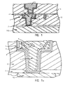
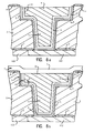
- Fig. 1 is part of a structure of the above described interconnect scheme of the prior art, showing two levels of metal interconnections, each level defined by a double damascene method.
- Fig. la is an enlarged view of cross-section of an interconnect; wherein, copper interconnect line 9 on one level is shown making contact to lower level metal interconnect line 102 through via-stud 11. It should be understood that in a double damascene method the via stud 11 and the conductor line 102 are an integral part of one another.
- the copper interconnect comprises an adhesive layer 5, an optional barrier layer 6; a PVD copper seed layer 8; bulk copper layer 9 and 11, and an inorganic insulator 4 atop polyimide insulator 3.
- Another object of the present invention is to provide a high conductivity copper based metallurgy with low dielectric constant polyimide passivation.
- It an objective of the present embodiment to provide electroplated copper interconnection lines with reduced PVD copper seed layer thickness to improve the electromigration resistance of the interconnect line.
- the method may thus include a double damascene method using electroplated copper, where a reduced thickness PVD layer is employed, or where the PVD layer is replaced by a conformal coating of CVD copper seed layer which has about three times higher electromigration resistance than that for the PVD deposited copper.
- the seed layer may also be converted to an intermetallic layer.
- a layer of a copper intermetallic such as hafnium, lanthanum, zirconium, tin and titanium is provided to improve the electromigration resistance and to reduce defect sensitivity.
- a method is thus described to form a cap which fully covers the surface on top of copper lines formed in the substrate to improve corrosion resistance. Structure and methods are also described to improve the electromigration and corrosion resistance by incorporating carbon atoms in copper interstitial positions.
- the substrate is then heated to react the intermetallic forming element with the copper layer to form a layer of intermetallic compound in the copper layer.
- the intermetallic forming element layer may be deposited before the copper layer or a copper layer is deposited before the intermetallic forming element layer. Also, the intermetallic forming element layer may be deposited before the copper layer, and a further intermetallic forming element layer may be deposited after the copper layer.
- the metallic liner, the layer of intermetallic forming element and the layer of copper may be deposited by common or separate deposition techniques selected from the group consisting of sputtering, evaporation and CVD.
- the metallic liner, the layer of intermetallic forming element and the layer of copper are in-situ deposited by sputtering in a single pump down, wherein the sputtering may be reactive sputtering, collimated sputtering, magnetron sputtering, low pressure sputtering, ECR sputtering, ionized beam sputtering and any combination thereof.
- a more preferred method relates to a method of forming reliable multilevel interconnections of copper lines, at sub-micron pitch and isolated from one another by low dielectric insulation to make contacts to electrical features in a substrate.
- the method comprises the steps of initially depositing a pair of insulation layers on a substrate having an electrical feature, photolithographically defining a via-studs pattern on at least one of the insulation layers, partially etching the pair of insulation layers, photolithographically defining an interconnection line pattern on at least one of the insulation layers, and etching the insulation layers until the electrical feature is exposed; thereby, forming trenches and holes in the pair of insulators. Subsequently, there is deposited a liner metallurgy in the trenches and holes.
- a layer of an element capable of forming an intermetallic compound with copper is deposited, as well as one or more layers of copper to fill the holes and trenches.
- the copper is polished to remove excess metal outside of the trenches and the substrate is heated to react the intermetallic forming element with copper to form a layer of an intermetallic compound with copper.
- One of the copper layers may be deposited by reactive sputtering of copper with a carbonaceous gas to incorporate carbon atoms within the lattice of deposited copper.
- the thickness of the intermetallic forming element is between about 100 angstroms and 600 angstroms.
- the intermetallic layer may be formed beneath copper in the holes and trenches, within copper in the holes and trenches, or above copper in the holes and trenches
- the present invention provides a substrate having interconnections of copper lines comprising a pair of insulation layers disposed on a substrate having an electrical feature, the insulation layers having etched via-stud patterns and etched interconnection line patterns forming holes and trenches in the pair of insulators.
- a metallic layer lines the trenches and holes, and copper fills the holes and trenches, with a portion of the copper including therein a region of a copper intermetallic compound.
- a preferred embodiment relates to a method of providing copper interconnections having improved electromigration and corrosion resistance on a substrate having trenches comprising the steps of heating the substrate in a vacuum tool, introducing a carbonaceous material, in gaseous form, into the vacuum, and depositing copper metal in the substrate trenches while simultaneously incorporating interstitial atoms into the copper lattice to form copper lines in the trenches.
- the substrate is held at a temperature between 100 - 400° C during the deposition and the carbonaceous material is a hydrocarbon having the formula C x H y or C x H x and containing no oxygen, nitrogen or sulphur.
- an embodiment provides a substrate having interconnections of copper lines comprising a pair of insulation layers disposed on a substrate having an electrical feature, the insulation layers having etched via-stud patterns and etched interconnection line patterns forming holes and trenches in the pair of insulators, a metallic layer lining the trenches and holes, and copper filling the holes and trenches, the copper containing from about 0.1 to 15 ppm carbon.
- the invention in a further aspect, relates to a method of providing a protective cap on an substrate interconnection having a surface planar with surrounding insulation.
- the method comprises the steps of providing a substrate having an insulative layer thereon, etched via-stud patterns and etched interconnection line patterns forming holes and trenches within the insulative layer, and copper metallurgy filling the holes and trenches to an upper surface of the insulative layer to form a substrate interconnection. Then the copper is polished to recess its surface below the surrounding insulative layer surface. There is subsequently deposited a layer of a material for a cap over the recessed copper to a level above the surrounding insulative layer surface.
- the substrate is then polished to remove the cap material from regions outside of the substrate interconnection and form a cap surface planar with the surrounding insulative layer surface.
- the recess thickness is about 100 angstroms to 400 angstroms
- the material for the cap is selectively deposited and chosen from the group consisting of tungsten, tungsten-silicon, tungsten-nitrogen, hafnium, zirconium, tantalum, tantalum-nitride, titanium, tin, lanthanum, germanium, carbon, chromium, chromium-chromium oxide, tin, platinum, and, combinations thereof.
- the chemical vapor deposition copper layer may preferably have a thickness of about 50 to 2000 angstroms, more preferably about 100 to 700 angstroms.
- the physical vapor deposition may be by copper sputtering or by copper evaporation, and preferably the physical vapor deposition copper layer has a thickness below about 600 angstroms.
- the method may include the step of depositing in the pattern a layer of an element capable of forming an intermetallic compound with copper. Subsequent to depositing the layer of copper which substantially fills the pattern, the invention may include the step of heating the substrate to react the intermetallic forming element with the layer of copper which substantially fills the pattern to form a layer of intermetallic compound.
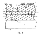
- FIG. 2 there is shown a cross-section of conventional silicon semiconductor structure comprised of a silicon substrate 105 having thereon various device contact studs (vias) 101 and local interconnects (lines) 102, typically tungsten with underlayers of titanium and titanium nitride (not shown) formed within insulator layers 106, 103, respectively.
- various device contact studs (vias) 101 and local interconnects (lines) 102 typically tungsten with underlayers of titanium and titanium nitride (not shown) formed within insulator layers 106, 103, respectively.
- the use of a thin layer of an insulator to prevent the formation of metal spikes between vias and lines, e.g., due to misalignment, is disclosed elsewhere and a description is not necessary in relation to the current invention.
- the method of the present invention forms reliable multilevel interconnections of copper lines, at sub-micron pitch, and isolated from one another by low dielectric insulation, making contacts to electrical features in a substrate.
- the substrate structure may be a semiconductor having plurality of electronic devices, an organic circuit carrier, or a ceramic circuit carrier.
- the local interconnects 102 are preferably formed by damascene methods of prior art, with the top surfaces of the local interconnects being substantially planar with the surface of surrounding insulator 103, typically deposited boro-silicate or phospho-silicate glass or SiO 2 .
- Dielectric insulator layers 2, 3 and 4 are next deposited to begin a process of forming high conductivity interconnections.
- the pair of insulators may be deposited by ECR, sputtering, Plasma Enhanced CVD, CVD, spin-coating or any combination of these methods.
- these insulators may be made of polyimide, silicon-nitride, alumina, silicon-dioxide, phospho-silicate glass, yttrium oxide, magnesium oxide, aero-gel, or any combination of these materials.
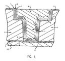
- a via-stud pattern is next defined atop insulator 4, for example, by a photolithographic process, followed by the step of etching insulator 4 and partially etching insulator 3 with suitable etchants.
- the pattern for the high conductivity metal interconnection lines is next defined, again, for example, by a photolithographic process, followed by etching remainder of insulator 3 and insulator 2 to form trenches 12 and holes 13 to expose metal line 102.
- liner materials and high conductivity metal of choice are deposited in accordance with the present invention, and polished by chemical-mechanical methods to remove excess metals, thereby simultaneously forming the via-stud and interconnection metal line patterns.
- the present invention is implemented at the point in the process where the combined via-stud and interconnection line patterns are etched in insulator layers 2, 3 and 4 to expose portions of local interconnect 102.
- Fig. 3 where only a portion of Fig. 2 is shown for clarity.
- a thin layer 5 typically 100 to 300 angstroms thick, of an adhesive and contact metal, preferably titanium, tantalum, tantalum nitride, tantalum, chromium, tungsten, or any combination of these layers.
- Layers 5 and 6 are referred to as the liner metallurgy employed in the present invention.
- the contact metal may be, for example, titanium, tantalum or tantalum-nitride, for example.
- the barrier material may be titanium-nitride, titanium-oxy-nitiride, tantalum, tantalum-nitride, chromium, chromium/chromium-oxide, tungsten, tungsten-nitride, tungsten-silicon, or any combination among them.
- the liner layers may be deposited by common or separate deposition techniques such as sputtering, evaporation.
- a sputtering technique is employed such as reactive sputtering, collimated sputtering, magnetron sputtering, low pressure sputtering, ECR sputtering, ionized beam sputtering or any combination of them. More preferably, these aforementioned depositions of layers 5 and 6 are carried out using collimated sputtering in a single pump down and using the technique for depositing reactive metals taught by Dalal and Lowney in U. S. Patent No. 4,379,832.
- the preferred deposition temperature is between about 120o and 400oC.
- a thin layer 7 preferably from about 100 to 600 angstroms thick, of an element which is capable of forming an intermetallic compound with copper.
- element may be selected from the group consisting of hafnium, lanthanum, zirconium, tin and titanium.
- a thin copper seed layer 8 typically 600 to 2000 angstroms thick.
- Layers 5-8 may be deposited by common or separate deposition techniques such as sputtering, evaporation or CVD.
- a sputtering technique is employed such as reactive sputtering, collimated sputtering, magnetron sputtering, low pressure sputtering, ECR sputtering, ionized beam sputtering or any combination of them. More preferably, these aforementioned depositions of layers 5, 6, and 7 and 8 are carried out using collimated sputtering in a single pump down and employing the technique for depositing reactive metals taught by Dalal and Lowney in U.S. Patent No. 4,379,832.
- the preferred deposition temperature is between 120° - 400° C.
- the copper seed layer may also intentionally contain carbon in interstitial positions, for enhanced electromigration resistance, and will be discussed further below.
- a remaining layer 9 of copper is then electroplated to fill the trenches.
- layer 8 or 8 and 9 may be deposited by CVD methods.
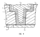
- the substrate wafers are then polished by chemical-mechanical methods to remove all excess metals from unpatterned areas, thereby, resulting the planarized structure shown in Fig. 3.
- intermetallic forming metal layer 7 If intermetallic forming metal layer 7 is used, the substrate wafers are next heated in a non-reactive atmosphere such as nitrogen to a temperature of about 250° - 450°C for 30 min. to 2 hours. This causes the intermetallic forming layer 7 to react with the copper layers to form a layer of copper intermetallic compound, 10 in Fig. 4.
- the copper intermetallic layer provides an improved electromigration resistance to the copper layers 8 and 9.
- the thickness of the intermetallic forming metal is preferably selected so as to consume all of the copper seed layer 8 (Fig. 3) during formation of the intermetallic compound.
- the intermetallic compounds formed in the copper layer by the present invention may be hafnium cupride (Hf 2 Cu), lanthanum cupride (LaCu 2 ), eta-bronze (Cu 6 Sn 5 ), titanium cupride (TiCu) and zirconium cupride (Zr 2 Cu).
- the intermetallic layer may be a complete intermetallic or a combination of intermetallic and constituent metal layers.
- the choice of intermetallic forming element may be based on two criteria. First, the chosen element preferably has no, or less than 2 atomic percent, solubility in copper. Low solubility is important as otherwise the element will diffuse into copper and affect its electrical conductivity. Second, the element preferably forms a stable intermetallic with copper. In addition to the above mentioned elements, any other elements which meet these criteria may be employed as the copper intermetallic-forming element.
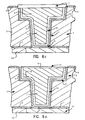
- the intermetallic layer is formed at the middle of the interconnection thickness, as shown in Fig 5a for small dimension via studs, and in Fig. 5b for a wider via-stud.
- intermetallic layer 7 is deposited after an initial layer of copper so as to form the intermetallic compound region away from the edges of the copper and toward the interior region.
- Fig. 5a shows the intermetallic region 10 after heat treatment (where the intermetallic element layer 7 was initially deposited) in a Y-shape in the interior of the copper layer 9.
- more than one intermetallic region may be employed, as shown in Fig. 5b where two regions of intermetallic element 7 were deposited in the location where intermetallic compound regions 10a and 10b are shown, after heat treatment.
- the intermetallic forming element is deposited on the top of the copper lines in the form of a cap.
- a thin layer of copper approximately 100 to 400 angstroms thick, is removed to recess its surface from the surrounding insulation surface. Removal may be by light chemical-mechanical polishing, mechanical polishing, or both, of the copper interconnect lines or via-studs to provide a planarized cap surface.
- a thin layer of an intermetallic forming element is next selectively deposited by the aforementioned methods (PVD, electroplating, electroless plating, CVD, or by any combination of them) preferably after in-situ sputter cleaning of the wafer. Excess metal from outside the interconnect trench is then removed by chemical-mechanical polishing, or simply mechanical polishing, leaving the cap of intermetallic forming element atop copper lines at the same level as the surface of layer 4, as shown in Fig. 6c. The next step is to heat treat the wafers, as described above, to form intermetallic layer 7 at the top of the copper layer 9. In Fig. 6d there is shown the embodiment where the intermetallic layer or region is formed both at the bottom and at the top of the copper interconnection layer.
- This method of forming an intermetallic cap layer has an advantage of fully covering the copper lines along the line edges, as opposed to leaving narrow slits of copper exposed, as in methods where cap metal is deposited along with the liner and copper. It should be understood that, whereas this method of forming a cap is described here with the objective of forming a cap of an intermetallic compound, the method is not limited to such metals, but any desired metal, alloy or intermetallic compound may be used, such as tungsten, tungsten-silicon, tungsten-nitrogen, hafnium, zirconium, tantalum, tantalum-nitride, titanium, tin, lanthanum, germanium, carbon, chromium, chromium-chromium oxide, tin, platinum, or any combination among them.
- the copper intermetallic layer is formed by selective deposition either at the bottom, in the middle, at the top of the copper line cross-section, or at any combination of these sites.
- the present invention provides a method to form in-situ a copper intermetallic layer at any or all of these regions to improve the electromigration resistance of copper interconnection lines.
- the copper seed layer is preferably deposited in a vacuum tool along with intentional bleeding of a carbonaceous material, in gaseous form.
- the substrate is preferably held at a temperature from about 100 - 400°C.
- the carbonaceous material is a hydrocarbon that does not contain oxygen, nitrogen or sulphur, such as those carbonaceous material belonging to the C x H y or C x H x hydrocarbon groups.
- the carbonaceous material may be introduced into the vacuum tool in concentrated form, or in a diluted form using an inert carrier gas.
- the vacuum tool is a sputtering or an evaporation tool, and the partial pressure of the carbonaceous material is from about 10 -4 to 10 -7 Torr.
- More preferred parameters of such deposition process are initially pumping down the substrate to a pressure of 10 -8 Torr, bleeding in acetylene gas at a pressure of 10 -5 Torr using an automatic pressure control, and subsequently introducing argon gas at a pressure of 4in. Torr and sputter depositing the copper into the trenches of the substrate.
- This aspect of the present invention provides an interconnection of copper having 0.1 ppm to 15 ppm dissolved carbon in the copper lattice.
- the copper seed layer 8 is deposited for the purpose of electroplating copper in next process step. If a choice is made to use CVD copper for layer 9, seed layer 8 is not needed.
- the pair of insulators could be organic/inorganic, organic/organic or inorganic/inorganic.
- the use of chemical vapor deposition to deposit the copper seed layer provides heretofore unknown advantages as compared to use of physical vapor deposition (e.g., sputtering or evaporation) techniques at the typical 1100 - 2000 angstrom thicknesses employed in the prior art.
- the CVD copper seed layer deposited may have a thickness range of about 50 - 2000 angstroms, preferably in the range of about 100 - 700 angstroms.
- a PVD copper seed layer when deposited at a thickness less than about 800 angstroms, preferably below about 600 angstroms, provides advantages over thicker prior art PVD copper seed layers. These advantages include higher electromigration resistance.
- the copper layer which fills the trench may be deposited directly on the copper seed layer without the copper intermetallic layer in accordance with the present invention. Copper layer should be deposited by a process different than that used to deposit the seed layer.
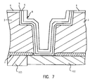
- Figs. 7 and 8 The interconnection of this aspect of the present invention is shown in Figs. 7 and 8.
- Fig. 7 which shows a portion of Fig. 2
- liner layers 5 and 6 are deposited in the same manner as previously described, with thermal diffusion layer 6 still being optional.
- seed layer 8 may be deposited directly on liner layer 6, or if layer 6 is not present, directly on liner layer 5. If a CVD technique is employed, the seed layer thickness 8 is more preferably in the range of about 300 to 600 angstroms.
- the copper seed layer is preferably less than about 600 angstroms, thick, more preferably about 200 to 500 angstroms thick.
- a remaining layer 9 of copper is electroplated to completely fill the trenches.
- the substrate wafers are then polished by chemical-mechanical methods to remove all excess metal from unpatterned areas, thereby resulting in the structure shown in Fig. 8.
- Such a structure may then provide sub-quarter-micron copper interconnections with improved electro-migration resistance and reduced defect sensitivity.
Landscapes
- Internal Circuitry In Semiconductor Integrated Circuit Devices (AREA)
- Electrodes Of Semiconductors (AREA)
Applications Claiming Priority (4)
| Application Number | Priority Date | Filing Date | Title |
|---|---|---|---|
| US08/866,777 US6130161A (en) | 1997-05-30 | 1997-05-30 | Method of forming copper interconnections with enhanced electromigration resistance and reduced defect sensitivity |
| US866777 | 1997-05-30 | ||
| US08/947,277 US6069068A (en) | 1997-05-30 | 1997-10-08 | Sub-quarter-micron copper interconnections with improved electromigration resistance and reduced defect sensitivity |
| US947277 | 1997-10-08 |
Publications (3)
| Publication Number | Publication Date |
|---|---|
| EP0881673A2 true EP0881673A2 (de) | 1998-12-02 |
| EP0881673A3 EP0881673A3 (de) | 1998-12-09 |
| EP0881673B1 EP0881673B1 (de) | 2006-10-11 |
Family
ID=27127969
Family Applications (1)
| Application Number | Title | Priority Date | Filing Date |
|---|---|---|---|
| EP98303611A Expired - Lifetime EP0881673B1 (de) | 1997-05-30 | 1998-05-08 | Kupferverdrahtung mit verbessertem Elektromigrationswiderstand und reduzierter Defektempfindlichkeit |
Country Status (6)
| Country | Link |
|---|---|
| US (2) | US6069068A (de) |
| EP (1) | EP0881673B1 (de) |
| JP (1) | JP3057054B2 (de) |
| KR (1) | KR100304395B1 (de) |
| DE (1) | DE69836114T2 (de) |
| TW (1) | TW437044B (de) |
Cited By (65)
| Publication number | Priority date | Publication date | Assignee | Title |
|---|---|---|---|---|
| GB2336469A (en) * | 1998-04-17 | 1999-10-20 | Nec Corp | Semiconductor device wiring |
| EP0982771A1 (de) * | 1998-08-28 | 2000-03-01 | Lucent Technologies Inc. | Verfahren zur Herstellung einer Halbleiterschaltung mit Kupfer-Verbindungsleitungen |
| WO2000011721A1 (en) * | 1998-08-20 | 2000-03-02 | The Government Of The United States Of America, Represented By The Secretary Of The Navy | Electronic devices with barrier film and process for making same |
| WO2000021120A1 (en) * | 1998-10-03 | 2000-04-13 | Applied Materials, Inc. | Method and apparatus for depositing material upon a semiconductor wafer using a transition chamber of a multiple chamber semiconductor wafer processing system |
| WO2000003420A3 (en) * | 1998-07-10 | 2000-06-29 | Cvc Inc | Method for forming a copper film on a substrate |
| US6083818A (en) * | 1998-08-20 | 2000-07-04 | The United States Of America As Represented By The Secretary Of The Navy | Electronic devices with strontium barrier film and process for making same |
| WO2000054330A1 (en) * | 1999-03-10 | 2000-09-14 | Advanced Micro Devices, Inc. | High-reliability damascene interconnect formation for semiconductor fabrication |
| WO2000075982A1 (en) * | 1999-06-09 | 2000-12-14 | Alliedsignal Inc. | Fabrication method for self aligned cu diffusion barrier in an integrated circuit |
| US6171953B1 (en) | 1998-08-20 | 2001-01-09 | The United States Of America As Represented By The Secretary Of The Navy | Processes for making electronic devices with rubidum barrier film |
| EP1083596A1 (de) * | 1999-09-07 | 2001-03-14 | Chartered Semiconductor Manufacturing Pte Ltd. | Verfahren zur Herstellung einer Kupfer-Dualdamaszen-Struktur mit verminderter Muldenbildung und Erosion |
| US6211066B1 (en) | 1998-08-20 | 2001-04-03 | The United States Of America As Represented By The Secretary Of The Navy | Electronic devices with barium barrier film and process for making same |
| US6245655B1 (en) | 1999-04-01 | 2001-06-12 | Cvc Products, Inc. | Method for planarized deposition of a material |
| US6274495B1 (en) | 1998-09-03 | 2001-08-14 | Cvc Products, Inc. | Method for fabricating a device on a substrate |
| US6291876B1 (en) | 1998-08-20 | 2001-09-18 | The United States Of America As Represented By The Secretary Of The Navy | Electronic devices with composite atomic barrier film and process for making same |
| US6294836B1 (en) | 1998-12-22 | 2001-09-25 | Cvc Products Inc. | Semiconductor chip interconnect barrier material and fabrication method |
| WO2001020647A3 (en) * | 1999-09-17 | 2002-01-17 | Nutool Inc | Novel chip interconnect and packaging deposition methods and structures |
| WO2001032951A3 (en) * | 1999-11-02 | 2002-01-17 | Univ Massachusetts | Chemical fluid deposition for the formation of metal and metal alloy films on patterned and unpatterned substrates |
| US6351036B1 (en) * | 1998-08-20 | 2002-02-26 | The United States Of America As Represented By The Secretary Of The Navy | Electronic devices with a barrier film and process for making same |
| US6375693B1 (en) | 1999-05-07 | 2002-04-23 | International Business Machines Corporation | Chemical-mechanical planarization of barriers or liners for copper metallurgy |
| US6444263B1 (en) | 2000-09-15 | 2002-09-03 | Cvc Products, Inc. | Method of chemical-vapor deposition of a material |
| US6465867B1 (en) * | 2001-02-21 | 2002-10-15 | Advanced Micro Devices, Inc. | Amorphous and gradated barrier layer for integrated circuit interconnects |
| US6465887B1 (en) | 2000-05-03 | 2002-10-15 | The United States Of America As Represented By The Secretary Of The Navy | Electronic devices with diffusion barrier and process for making same |
| US6471913B1 (en) | 2000-02-09 | 2002-10-29 | Semitool, Inc. | Method and apparatus for processing a microelectronic workpiece including an apparatus and method for executing a processing step at an elevated temperature |
| DE10127934A1 (de) * | 2001-06-08 | 2002-12-19 | Infineon Technologies Ag | Leiterbahnanordnung und Verfahren zum Herstellen einer gekapselten Leiterbahnkopplung |
| US6508920B1 (en) | 1998-02-04 | 2003-01-21 | Semitool, Inc. | Apparatus for low-temperature annealing of metallization microstructures in the production of a microelectronic device |
| EP1063687A3 (de) * | 1999-05-24 | 2003-03-19 | Lucent Technologies Inc. | Titan-Tantal-Barriereschicht und Verfahren zu deren Herstellung |
| WO2003063209A2 (en) | 2002-01-18 | 2003-07-31 | Intel Corporation | Copper interconnect doped with carbon and silicon |
| EP1102315A3 (de) * | 1999-11-15 | 2003-09-24 | Chartered Semiconductor Manufacturing Pte Ltd. | Verfahren zum Vermeiden von Kupfer-Kontamination der Seitenflächen eines Kontaktloches oder einer Doppel-Damaszenen-Struktur |
| US6627995B2 (en) | 2000-03-03 | 2003-09-30 | Cvc Products, Inc. | Microelectronic interconnect material with adhesion promotion layer and fabrication method |
| WO2003052798A3 (en) * | 2001-12-13 | 2003-10-16 | Advanced Micro Devices Inc | Method for improving electromigration performance of metallization features through multiple depositions of binary alloys |
| US6689700B1 (en) | 1999-11-02 | 2004-02-10 | University Of Massachusetts | Chemical fluid deposition method for the formation of metal and metal alloy films on patterned and unpatterned substrates |
| US6720654B2 (en) | 1998-08-20 | 2004-04-13 | The United States Of America As Represented By The Secretary Of The Navy | Electronic devices with cesium barrier film and process for making same |
| KR100435784B1 (ko) * | 2001-12-21 | 2004-06-12 | 동부전자 주식회사 | 반도체 소자의 금속배선 형성 방법 |
| US6753251B2 (en) | 1998-02-04 | 2004-06-22 | Semitool, Inc. | Method for filling recessed micro-structures with metallization in the production of a microelectronic device |
| US6780374B2 (en) | 2000-12-08 | 2004-08-24 | Semitool, Inc. | Method and apparatus for processing a microelectronic workpiece at an elevated temperature |
| WO2004088745A1 (ja) | 2003-03-28 | 2004-10-14 | Fujitsu Limited | 半導体装置 |
| WO2005004234A1 (en) * | 2003-07-03 | 2005-01-13 | International Business Machines Corporation | Selective capping of copper wiring |
| US6916412B2 (en) | 1999-04-13 | 2005-07-12 | Semitool, Inc. | Adaptable electrochemical processing chamber |
| US6929774B2 (en) | 1997-07-10 | 2005-08-16 | Applied Materials, Inc. | Method and apparatus for heating and cooling substrates |
| US7020537B2 (en) | 1999-04-13 | 2006-03-28 | Semitool, Inc. | Tuning electrodes used in a reactor for electrochemically processing a microelectronic workpiece |
| EP1649510A2 (de) * | 2003-06-23 | 2006-04-26 | International Business Machines Corporation | Doppel-damascene-verbindungsstrukturen mit verschiedenen materialien für leitungs- und kontaktlochleiter |
| US7041595B2 (en) | 1999-08-27 | 2006-05-09 | Micron Technology, Inc. | Method of forming a barrier seed layer with graded nitrogen composition |
| US7090751B2 (en) | 2001-08-31 | 2006-08-15 | Semitool, Inc. | Apparatus and methods for electrochemical processing of microelectronic workpieces |
| US7102763B2 (en) | 2000-07-08 | 2006-09-05 | Semitool, Inc. | Methods and apparatus for processing microelectronic workpieces using metrology |
| US7115196B2 (en) | 1998-03-20 | 2006-10-03 | Semitool, Inc. | Apparatus and method for electrochemically depositing metal on a semiconductor workpiece |
| US7129161B2 (en) | 2001-07-19 | 2006-10-31 | Trikon Holdings Limited | Depositing a tantalum film |
| US7147760B2 (en) | 1998-07-10 | 2006-12-12 | Semitool, Inc. | Electroplating apparatus with segmented anode array |
| US7160421B2 (en) | 1999-04-13 | 2007-01-09 | Semitool, Inc. | Turning electrodes used in a reactor for electrochemically processing a microelectronic workpiece |
| US7189318B2 (en) | 1999-04-13 | 2007-03-13 | Semitool, Inc. | Tuning electrodes used in a reactor for electrochemically processing a microelectronic workpiece |
| US7264698B2 (en) | 1999-04-13 | 2007-09-04 | Semitool, Inc. | Apparatus and methods for electrochemical processing of microelectronic workpieces |
| US7267749B2 (en) | 1999-04-13 | 2007-09-11 | Semitool, Inc. | Workpiece processor having processing chamber with improved processing fluid flow |
| US7311810B2 (en) | 2003-04-18 | 2007-12-25 | Applied Materials, Inc. | Two position anneal chamber |
| US7341947B2 (en) | 2002-03-29 | 2008-03-11 | Micron Technology, Inc. | Methods of forming metal-containing films over surfaces of semiconductor substrates |
| US7351315B2 (en) | 2003-12-05 | 2008-04-01 | Semitool, Inc. | Chambers, systems, and methods for electrochemically processing microfeature workpieces |
| US7351314B2 (en) | 2003-12-05 | 2008-04-01 | Semitool, Inc. | Chambers, systems, and methods for electrochemically processing microfeature workpieces |
| US7371306B2 (en) | 2003-06-06 | 2008-05-13 | Semitool, Inc. | Integrated tool with interchangeable wet processing components for processing microfeature workpieces |
| US7393439B2 (en) | 2003-06-06 | 2008-07-01 | Semitool, Inc. | Integrated microfeature workpiece processing tools with registration systems for paddle reactors |
| US7419772B2 (en) | 2001-11-21 | 2008-09-02 | University Of Massachusetts | Mesoporous materials and methods |
| US7423345B2 (en) | 2002-03-29 | 2008-09-09 | Micron Technology, Inc. | Semiconductor constructions comprising a layer of metal over a substrate |
| US7438788B2 (en) | 1999-04-13 | 2008-10-21 | Semitool, Inc. | Apparatus and methods for electrochemical processing of microelectronic workpieces |
| US7585398B2 (en) | 1999-04-13 | 2009-09-08 | Semitool, Inc. | Chambers, systems, and methods for electrochemically processing microfeature workpieces |
| DE19953843B4 (de) * | 1999-04-13 | 2009-10-01 | Hyundai Electronics Industries Co., Ltd., Ichon | Verfahren zur Herstellung einer Kupferverdrahtung für eine Halbleitervorrichtung |
| FR2963160A1 (fr) * | 2010-07-22 | 2012-01-27 | St Microelectronics Crolles 2 | Procede de realisation d'un niveau de metallisation et d'un niveau de via et circuit integre correspondant |
| US10096547B2 (en) | 1999-10-02 | 2018-10-09 | Uri Cohen | Metallic interconnects products |
| CN110931443A (zh) * | 2018-09-20 | 2020-03-27 | 三星电子株式会社 | 半导体装置和包括其的半导体封装件 |
Families Citing this family (121)
| Publication number | Priority date | Publication date | Assignee | Title |
|---|---|---|---|---|
| US6429120B1 (en) * | 2000-01-18 | 2002-08-06 | Micron Technology, Inc. | Methods and apparatus for making integrated-circuit wiring from copper, silver, gold, and other metals |
| US7510961B2 (en) | 1997-02-14 | 2009-03-31 | Micron Technology, Inc. | Utilization of energy absorbing layer to improve metal flow and fill in a novel interconnect structure |
| US6130161A (en) * | 1997-05-30 | 2000-10-10 | International Business Machines Corporation | Method of forming copper interconnections with enhanced electromigration resistance and reduced defect sensitivity |
| US6069068A (en) * | 1997-05-30 | 2000-05-30 | International Business Machines Corporation | Sub-quarter-micron copper interconnections with improved electromigration resistance and reduced defect sensitivity |
| US6037248A (en) * | 1997-06-13 | 2000-03-14 | Micron Technology, Inc. | Method of fabricating integrated circuit wiring with low RC time delay |
| JP3545177B2 (ja) | 1997-09-18 | 2004-07-21 | 株式会社荏原製作所 | 多層埋め込みCu配線形成方法 |
| US6174811B1 (en) * | 1998-12-02 | 2001-01-16 | Applied Materials, Inc. | Integrated deposition process for copper metallization |
| US6211073B1 (en) | 1998-02-27 | 2001-04-03 | Micron Technology, Inc. | Methods for making copper and other metal interconnections in integrated circuits |
| US6632292B1 (en) | 1998-03-13 | 2003-10-14 | Semitool, Inc. | Selective treatment of microelectronic workpiece surfaces |
| TW593731B (en) | 1998-03-20 | 2004-06-21 | Semitool Inc | Apparatus for applying a metal structure to a workpiece |
| US6197181B1 (en) * | 1998-03-20 | 2001-03-06 | Semitool, Inc. | Apparatus and method for electrolytically depositing a metal on a microelectronic workpiece |
| US6268289B1 (en) * | 1998-05-18 | 2001-07-31 | Motorola Inc. | Method for protecting the edge exclusion of a semiconductor wafer from copper plating through use of an edge exclusion masking layer |
| US6284656B1 (en) * | 1998-08-04 | 2001-09-04 | Micron Technology, Inc. | Copper metallurgy in integrated circuits |
| US6150257A (en) * | 1998-08-28 | 2000-11-21 | Micron Technology, Inc. | Plasma treatment of an interconnect surface during formation of an interlayer dielectric |
| US6288442B1 (en) | 1998-09-10 | 2001-09-11 | Micron Technology, Inc. | Integrated circuit with oxidation-resistant polymeric layer |
| KR100546173B1 (ko) * | 1998-09-21 | 2006-04-14 | 주식회사 하이닉스반도체 | 반도체소자의 금속배선 형성방법 |
| US6815336B1 (en) * | 1998-09-25 | 2004-11-09 | Taiwan Semiconductor Manufacturing Company, Ltd. | Planarization of copper damascene using reverse current electroplating and chemical mechanical polishing |
| US6362526B1 (en) * | 1998-10-08 | 2002-03-26 | Advanced Micro Devices, Inc. | Alloy barrier layers for semiconductors |
| US6200906B1 (en) * | 1998-12-17 | 2001-03-13 | Micron Technology, Inc. | Stepped photoresist profile and opening formed using the profile |
| KR100559030B1 (ko) * | 1998-12-30 | 2006-06-16 | 주식회사 하이닉스반도체 | 반도체 소자의 구리 금속 배선 형성 방법 |
| TW426980B (en) * | 1999-01-23 | 2001-03-21 | Lucent Technologies Inc | Wire bonding to copper |
| US20020127845A1 (en) * | 1999-03-01 | 2002-09-12 | Paul A. Farrar | Conductive structures in integrated circuits |
| US7192494B2 (en) | 1999-03-05 | 2007-03-20 | Applied Materials, Inc. | Method and apparatus for annealing copper films |
| US6362099B1 (en) * | 1999-03-09 | 2002-03-26 | Applied Materials, Inc. | Method for enhancing the adhesion of copper deposited by chemical vapor deposition |
| US6235633B1 (en) * | 1999-04-12 | 2001-05-22 | Taiwan Semiconductor Manufacturing Company | Method for making tungsten metal plugs in a polymer low-K intermetal dielectric layer using an improved two-step chemical/mechanical polishing process |
| US6146517A (en) * | 1999-05-19 | 2000-11-14 | Infineon Technologies North America Corp. | Integrated circuits with copper metallization for interconnections |
| JP2000349085A (ja) | 1999-06-01 | 2000-12-15 | Nec Corp | 半導体装置及び半導体装置の製造方法 |
| KR100333712B1 (ko) * | 1999-06-24 | 2002-04-24 | 박종섭 | 반도체 소자의 상감형 금속배선 형성방법 |
| US6627542B1 (en) * | 1999-07-12 | 2003-09-30 | Applied Materials, Inc. | Continuous, non-agglomerated adhesion of a seed layer to a barrier layer |
| US6328871B1 (en) * | 1999-08-16 | 2001-12-11 | Applied Materials, Inc. | Barrier layer for electroplating processes |
| US6399479B1 (en) * | 1999-08-30 | 2002-06-04 | Applied Materials, Inc. | Processes to improve electroplating fill |
| US6610596B1 (en) * | 1999-09-15 | 2003-08-26 | Samsung Electronics Co., Ltd. | Method of forming metal interconnection using plating and semiconductor device manufactured by the method |
| US6136707A (en) * | 1999-10-02 | 2000-10-24 | Cohen; Uri | Seed layers for interconnects and methods for fabricating such seed layers |
| US6610151B1 (en) * | 1999-10-02 | 2003-08-26 | Uri Cohen | Seed layers for interconnects and methods and apparatus for their fabrication |
| US6924226B2 (en) * | 1999-10-02 | 2005-08-02 | Uri Cohen | Methods for making multiple seed layers for metallic interconnects |
| US6727169B1 (en) * | 1999-10-15 | 2004-04-27 | Asm International, N.V. | Method of making conformal lining layers for damascene metallization |
| US6458251B1 (en) * | 1999-11-16 | 2002-10-01 | Applied Materials, Inc. | Pressure modulation method to obtain improved step coverage of seed layer |
| US6420262B1 (en) | 2000-01-18 | 2002-07-16 | Micron Technology, Inc. | Structures and methods to enhance copper metallization |
| US7211512B1 (en) * | 2000-01-18 | 2007-05-01 | Micron Technology, Inc. | Selective electroless-plated copper metallization |
| US7262130B1 (en) * | 2000-01-18 | 2007-08-28 | Micron Technology, Inc. | Methods for making integrated-circuit wiring from copper, silver, gold, and other metals |
| US6455425B1 (en) * | 2000-01-18 | 2002-09-24 | Advanced Micro Devices, Inc. | Selective deposition process for passivating top interface of damascene-type Cu interconnect lines |
| US6376370B1 (en) | 2000-01-18 | 2002-04-23 | Micron Technology, Inc. | Process for providing seed layers for using aluminum, copper, gold and silver metallurgy process for providing seed layers for using aluminum, copper, gold and silver metallurgy |
| JP4064595B2 (ja) * | 2000-03-28 | 2008-03-19 | 株式会社東芝 | 半導体装置の製造方法 |
| JP3449960B2 (ja) * | 2000-02-25 | 2003-09-22 | 沖電気工業株式会社 | 半導体装置の製造方法 |
| JP3651765B2 (ja) * | 2000-03-27 | 2005-05-25 | 株式会社東芝 | 半導体装置 |
| JP2001319928A (ja) * | 2000-05-08 | 2001-11-16 | Hitachi Ltd | 半導体集積回路装置およびその製造方法 |
| US6674167B1 (en) * | 2000-05-31 | 2004-01-06 | Micron Technology, Inc. | Multilevel copper interconnect with double passivation |
| US6423629B1 (en) * | 2000-05-31 | 2002-07-23 | Kie Y. Ahn | Multilevel copper interconnects with low-k dielectrics and air gaps |
| JP2002009248A (ja) * | 2000-06-26 | 2002-01-11 | Oki Electric Ind Co Ltd | キャパシタおよびその製造方法 |
| JPWO2002037558A1 (ja) * | 2000-11-02 | 2004-03-11 | 富士通株式会社 | 半導体装置及びその製造方法 |
| US6433402B1 (en) * | 2000-11-16 | 2002-08-13 | Advanced Micro Devices, Inc. | Selective copper alloy deposition |
| US6627052B2 (en) | 2000-12-12 | 2003-09-30 | International Business Machines Corporation | Electroplating apparatus with vertical electrical contact |
| US6503641B2 (en) * | 2000-12-18 | 2003-01-07 | International Business Machines Corporation | Interconnects with Ti-containing liners |
| US20020081845A1 (en) * | 2000-12-27 | 2002-06-27 | Novellus Systems, Inc. | Method for the formation of diffusion barrier |
| KR101050377B1 (ko) | 2001-02-12 | 2011-07-20 | 에이에스엠 아메리카, 인코포레이티드 | 반도체 박막 증착을 위한 개선된 공정 |
| US6429524B1 (en) * | 2001-05-11 | 2002-08-06 | International Business Machines Corporation | Ultra-thin tantalum nitride copper interconnect barrier |
| JP3530149B2 (ja) * | 2001-05-21 | 2004-05-24 | 新光電気工業株式会社 | 配線基板の製造方法及び半導体装置 |
| KR100499557B1 (ko) * | 2001-06-11 | 2005-07-07 | 주식회사 하이닉스반도체 | 반도체소자의 배선 형성방법 |
| US6656834B1 (en) * | 2001-06-20 | 2003-12-02 | Advanced Micro Devices, Inc. | Method of selectively alloying interconnect regions by deposition process |
| US6900119B2 (en) * | 2001-06-28 | 2005-05-31 | Micron Technology, Inc. | Agglomeration control using early transition metal alloys |
| US20030008243A1 (en) * | 2001-07-09 | 2003-01-09 | Micron Technology, Inc. | Copper electroless deposition technology for ULSI metalization |
| US6703308B1 (en) | 2001-11-26 | 2004-03-09 | Advanced Micro Devices, Inc. | Method of inserting alloy elements to reduce copper diffusion and bulk diffusion |
| US6835655B1 (en) * | 2001-11-26 | 2004-12-28 | Advanced Micro Devices, Inc. | Method of implanting copper barrier material to improve electrical performance |
| US6703307B2 (en) | 2001-11-26 | 2004-03-09 | Advanced Micro Devices, Inc. | Method of implantation after copper seed deposition |
| US7696092B2 (en) | 2001-11-26 | 2010-04-13 | Globalfoundries Inc. | Method of using ternary copper alloy to obtain a low resistance and large grain size interconnect |
| US20030118798A1 (en) | 2001-12-25 | 2003-06-26 | Nec Electronics Corporation | Copper interconnection and the method for fabricating the same |
| US6861349B1 (en) | 2002-05-15 | 2005-03-01 | Advanced Micro Devices, Inc. | Method of forming an adhesion layer with an element reactive with a barrier layer |
| US6849173B1 (en) | 2002-06-12 | 2005-02-01 | Taiwan Semiconductor Manufacturing Company, Ltd. | Technique to enhance the yield of copper interconnections |
| US6717266B1 (en) * | 2002-06-18 | 2004-04-06 | Advanced Micro Devices, Inc. | Use of an alloying element to form a stable oxide layer on the surface of metal features |
| KR100443796B1 (ko) * | 2002-06-29 | 2004-08-11 | 주식회사 하이닉스반도체 | 구리 금속 배선 형성방법 |
| KR100456259B1 (ko) * | 2002-07-15 | 2004-11-09 | 주식회사 하이닉스반도체 | 반도체 소자의 구리 배선 형성방법 |
| US7186630B2 (en) * | 2002-08-14 | 2007-03-06 | Asm America, Inc. | Deposition of amorphous silicon-containing films |
| US7025866B2 (en) * | 2002-08-21 | 2006-04-11 | Micron Technology, Inc. | Microelectronic workpiece for electrochemical deposition processing and methods of manufacturing and using such microelectronic workpieces |
| US7001841B2 (en) * | 2002-08-26 | 2006-02-21 | Matsushita Electric Industrial Co., Ltd. | Production method of semiconductor device |
| US20040058526A1 (en) * | 2002-09-24 | 2004-03-25 | Infineon Technologies North America Corp. | Via liner integration to avoid resistance shift and resist mechanical stress |
| US7101790B2 (en) * | 2003-03-28 | 2006-09-05 | Taiwan Semiconductor Manufacturing Co., Ltd. | Method of forming a robust copper interconnect by dilute metal doping |
| US6825561B1 (en) | 2003-06-19 | 2004-11-30 | International Business Machines Corporation | Structure and method for eliminating time dependent dielectric breakdown failure of low-k material |
| US7220665B2 (en) * | 2003-08-05 | 2007-05-22 | Micron Technology, Inc. | H2 plasma treatment |
| US7169706B2 (en) * | 2003-10-16 | 2007-01-30 | Advanced Micro Devices, Inc. | Method of using an adhesion precursor layer for chemical vapor deposition (CVD) copper deposition |
| US20050092611A1 (en) * | 2003-11-03 | 2005-05-05 | Semitool, Inc. | Bath and method for high rate copper deposition |
| KR100573897B1 (ko) * | 2003-12-30 | 2006-04-26 | 동부일렉트로닉스 주식회사 | 반도체 제조 방법 |
| KR100564801B1 (ko) * | 2003-12-30 | 2006-03-28 | 동부아남반도체 주식회사 | 반도체 제조 방법 |
| KR100538444B1 (ko) * | 2003-12-31 | 2005-12-22 | 동부아남반도체 주식회사 | 비아 홀 및 트렌치 형성 방법 |
| JP2005203672A (ja) | 2004-01-19 | 2005-07-28 | Sony Corp | 半導体装置の製造方法 |
| US7128821B2 (en) * | 2004-01-20 | 2006-10-31 | Taiwan Semiconductor Manufacturing Co., Ltd. | Electropolishing method for removing particles from wafer surface |
| JP2005244178A (ja) | 2004-01-26 | 2005-09-08 | Toshiba Corp | 半導体装置の製造方法 |
| JP4224434B2 (ja) * | 2004-06-30 | 2009-02-12 | パナソニック株式会社 | 半導体装置及びその製造方法 |
| JP2006216746A (ja) | 2005-02-03 | 2006-08-17 | Sony Corp | 半導体装置 |
| US7438760B2 (en) * | 2005-02-04 | 2008-10-21 | Asm America, Inc. | Methods of making substitutionally carbon-doped crystalline Si-containing materials by chemical vapor deposition |
| JP2006253645A (ja) | 2005-02-14 | 2006-09-21 | Sony Corp | 半導体装置の製造方法および半導体装置 |
| JP2007081113A (ja) * | 2005-09-14 | 2007-03-29 | Sony Corp | 半導体装置の製造方法 |
| US7713876B2 (en) * | 2005-09-28 | 2010-05-11 | Tokyo Electron Limited | Method for integrating a ruthenium layer with bulk copper in copper metallization |
| CN1983550A (zh) * | 2005-12-14 | 2007-06-20 | 中芯国际集成电路制造(上海)有限公司 | 提高可靠性和成品率的消除铜位错的方法 |
| KR20080089403A (ko) * | 2005-12-22 | 2008-10-06 | 에이에스엠 아메리카, 인코포레이티드 | 도핑된 반도체 물질들의 에피택시 증착 |
| JP4676350B2 (ja) | 2006-02-14 | 2011-04-27 | ルネサスエレクトロニクス株式会社 | 半導体装置およびその製造方法 |
| US8278176B2 (en) | 2006-06-07 | 2012-10-02 | Asm America, Inc. | Selective epitaxial formation of semiconductor films |
| US7694413B2 (en) * | 2006-06-30 | 2010-04-13 | Intel Corporation | Method of making a bottomless via |
| US8212331B1 (en) * | 2006-10-02 | 2012-07-03 | Newport Fab, Llc | Method for fabricating a backside through-wafer via in a processed wafer and related structure |
| US8791018B2 (en) * | 2006-12-19 | 2014-07-29 | Spansion Llc | Method of depositing copper using physical vapor deposition |
| US20080265416A1 (en) * | 2007-04-27 | 2008-10-30 | Shen-Nan Lee | Metal line formation using advaced CMP slurry |
| US7759199B2 (en) * | 2007-09-19 | 2010-07-20 | Asm America, Inc. | Stressor for engineered strain on channel |
| US7939447B2 (en) * | 2007-10-26 | 2011-05-10 | Asm America, Inc. | Inhibitors for selective deposition of silicon containing films |
| US7655543B2 (en) * | 2007-12-21 | 2010-02-02 | Asm America, Inc. | Separate injection of reactive species in selective formation of films |
| KR100924556B1 (ko) | 2008-01-04 | 2009-11-02 | 주식회사 하이닉스반도체 | 반도체 소자의 금속배선 및 그 형성방법 |
| JP2008252103A (ja) * | 2008-04-21 | 2008-10-16 | Nec Electronics Corp | 半導体装置及び半導体装置の製造方法 |
| US7859114B2 (en) * | 2008-07-29 | 2010-12-28 | International Business Machines Corporation | IC chip and design structure with through wafer vias dishing correction |
| US8166651B2 (en) * | 2008-07-29 | 2012-05-01 | International Business Machines Corporation | Through wafer vias with dishing correction methods |
| US7807568B2 (en) * | 2008-10-23 | 2010-10-05 | Applied Materials, Inc. | Methods for reducing damage to substrate layers in deposition processes |
| US8486191B2 (en) * | 2009-04-07 | 2013-07-16 | Asm America, Inc. | Substrate reactor with adjustable injectors for mixing gases within reaction chamber |
| US8367528B2 (en) * | 2009-11-17 | 2013-02-05 | Asm America, Inc. | Cyclical epitaxial deposition and etch |
| US8809170B2 (en) | 2011-05-19 | 2014-08-19 | Asm America Inc. | High throughput cyclical epitaxial deposition and etch process |
| JP2013105753A (ja) * | 2011-11-10 | 2013-05-30 | Toshiba Corp | 半導体装置の製造方法 |
| US9059255B2 (en) * | 2013-03-01 | 2015-06-16 | Globalfoundries Inc. | Methods of forming non-continuous conductive layers for conductive structures on an integrated circuit product |
| JP5817856B2 (ja) * | 2014-01-27 | 2015-11-18 | 富士通セミコンダクター株式会社 | 半導体装置 |
| CN103839604A (zh) * | 2014-02-26 | 2014-06-04 | 京东方科技集团股份有限公司 | 导电膜及其制备方法、阵列基板 |
| US9496174B2 (en) | 2014-07-24 | 2016-11-15 | Qualcomm Incorporated | Mitigating electromigration, in-rush current effects, IR-voltage drop, and jitter through metal line and via matrix insertion |
| US10461026B2 (en) * | 2016-06-30 | 2019-10-29 | International Business Machines Corporation | Techniques to improve reliability in Cu interconnects using Cu intermetallics |
| JP6083846B1 (ja) * | 2016-09-30 | 2017-02-22 | 久美代 森田 | 糠床の水取り容器 |
| CN112247825B (zh) * | 2020-09-04 | 2021-09-28 | 北京烁科精微电子装备有限公司 | 一种芯片研磨方法 |
| WO2022088092A1 (zh) * | 2020-10-30 | 2022-05-05 | 华为技术有限公司 | 膜层穿孔的形成方法、半导体器件及芯片 |
| US20250132200A1 (en) * | 2023-10-18 | 2025-04-24 | Taiwan Semiconductor Manufacturing Company, Ltd. | Semiconductor structure and manufacturing method thereof |
Family Cites Families (36)
| Publication number | Priority date | Publication date | Assignee | Title |
|---|---|---|---|---|
| US4007039A (en) * | 1975-03-17 | 1977-02-08 | Olin Corporation | Copper base alloys with high strength and high electrical conductivity |
| US4017890A (en) * | 1975-10-24 | 1977-04-12 | International Business Machines Corporation | Intermetallic compound layer in thin films for improved electromigration resistance |
| US4153518A (en) * | 1977-11-18 | 1979-05-08 | Tektronix, Inc. | Method of making a metalized substrate having a thin film barrier layer |
| US4379832A (en) * | 1981-08-31 | 1983-04-12 | International Business Machines Corporation | Method for making low barrier Schottky devices of the electron beam evaporation of reactive metals |
| US4406858A (en) * | 1981-12-30 | 1983-09-27 | General Electric Company | Copper-base alloys containing strengthening and ductilizing amounts of hafnium and zirconium and method |
| US4920071A (en) * | 1985-03-15 | 1990-04-24 | Fairchild Camera And Instrument Corporation | High temperature interconnect system for an integrated circuit |
| US4749548A (en) * | 1985-09-13 | 1988-06-07 | Mitsubishi Kinzoku Kabushiki Kaisha | Copper alloy lead material for use in semiconductor device |
| US4789648A (en) * | 1985-10-28 | 1988-12-06 | International Business Machines Corporation | Method for producing coplanar multi-level metal/insulator films on a substrate and for forming patterned conductive lines simultaneously with stud vias |
| JPS6373660A (ja) * | 1986-09-17 | 1988-04-04 | Fujitsu Ltd | 半導体装置 |
| US5316974A (en) * | 1988-12-19 | 1994-05-31 | Texas Instruments Incorporated | Integrated circuit copper metallization process using a lift-off seed layer and a thick-plated conductor layer |
| US5250329A (en) * | 1989-04-06 | 1993-10-05 | Microelectronics And Computer Technology Corporation | Method of depositing conductive lines on a dielectric |
| US5256565A (en) * | 1989-05-08 | 1993-10-26 | The United States Of America As Represented By The United States Department Of Energy | Electrochemical planarization |
| JPH03244126A (ja) * | 1990-02-22 | 1991-10-30 | Toshiba Corp | 半導体装置の製造方法 |
| JPH05504790A (ja) * | 1990-04-03 | 1993-07-22 | インターナシヨナル・ビジネス・マシーンズ・コーポレーシヨン | 高純度金属の低温化学気相付着のための製造システム |
| US5273775A (en) * | 1990-09-12 | 1993-12-28 | Air Products And Chemicals, Inc. | Process for selectively depositing copper aluminum alloy onto a substrate |
| US5266446A (en) * | 1990-11-15 | 1993-11-30 | International Business Machines Corporation | Method of making a multilayer thin film structure |
| US5187300A (en) * | 1991-02-04 | 1993-02-16 | Air Products And Chemicals, Inc. | Volatile precursors for copper CVD |
| US5231751A (en) * | 1991-10-29 | 1993-08-03 | International Business Machines Corporation | Process for thin film interconnect |
| US5252516A (en) * | 1992-02-20 | 1993-10-12 | International Business Machines Corporation | Method for producing interlevel stud vias |
| US5300813A (en) * | 1992-02-26 | 1994-04-05 | International Business Machines Corporation | Refractory metal capped low resistivity metal conductor lines and vias |
| US5434451A (en) * | 1993-01-19 | 1995-07-18 | International Business Machines Corporation | Tungsten liner process for simultaneous formation of integral contact studs and interconnect lines |
| US5322712A (en) * | 1993-05-18 | 1994-06-21 | Air Products And Chemicals, Inc. | Process for improved quality of CVD copper films |
| US5380546A (en) * | 1993-06-09 | 1995-01-10 | Microelectronics And Computer Technology Corporation | Multilevel metallization process for electronic components |
| JP3632981B2 (ja) * | 1993-08-16 | 2005-03-30 | 株式会社東芝 | 多層配線基板および多層配線装置の製造方法 |
| US5391517A (en) * | 1993-09-13 | 1995-02-21 | Motorola Inc. | Process for forming copper interconnect structure |
| JPH08102463A (ja) * | 1994-09-30 | 1996-04-16 | Mitsubishi Electric Corp | 集積回路、その製造方法およびその薄膜形成装置 |
| US5565707A (en) * | 1994-10-31 | 1996-10-15 | International Business Machines Corporation | Interconnect structure using a Al2 Cu for an integrated circuit chip |
| JP3517802B2 (ja) * | 1995-09-01 | 2004-04-12 | 富士通株式会社 | 埋め込み導電層の形成方法 |
| US5877087A (en) * | 1995-11-21 | 1999-03-02 | Applied Materials, Inc. | Low temperature integrated metallization process and apparatus |
| JP3323055B2 (ja) | 1996-04-03 | 2002-09-09 | 株式会社東芝 | 半導体装置およびその製造方法 |
| US5814557A (en) * | 1996-05-20 | 1998-09-29 | Motorola, Inc. | Method of forming an interconnect structure |
| US6130161A (en) | 1997-05-30 | 2000-10-10 | International Business Machines Corporation | Method of forming copper interconnections with enhanced electromigration resistance and reduced defect sensitivity |
| US6069068A (en) * | 1997-05-30 | 2000-05-30 | International Business Machines Corporation | Sub-quarter-micron copper interconnections with improved electromigration resistance and reduced defect sensitivity |
| US5821168A (en) * | 1997-07-16 | 1998-10-13 | Motorola, Inc. | Process for forming a semiconductor device |
| US5897375A (en) * | 1997-10-20 | 1999-04-27 | Motorola, Inc. | Chemical mechanical polishing (CMP) slurry for copper and method of use in integrated circuit manufacture |
| US6074499A (en) * | 1998-01-09 | 2000-06-13 | South Dakoga School Of Mines And Technology | Boron-copper-magnesium-tin alloy and method for making same |
-
1997
- 1997-10-08 US US08/947,277 patent/US6069068A/en not_active Expired - Fee Related
-
1998
- 1998-05-08 EP EP98303611A patent/EP0881673B1/de not_active Expired - Lifetime
- 1998-05-08 DE DE69836114T patent/DE69836114T2/de not_active Expired - Lifetime
- 1998-05-26 JP JP10143914A patent/JP3057054B2/ja not_active Expired - Fee Related
- 1998-05-28 TW TW087108346A patent/TW437044B/zh not_active IP Right Cessation
- 1998-05-30 KR KR1019980020129A patent/KR100304395B1/ko not_active Expired - Fee Related
-
1999
- 1999-12-10 US US09/459,167 patent/US6258710B1/en not_active Expired - Fee Related
Cited By (99)
| Publication number | Priority date | Publication date | Assignee | Title |
|---|---|---|---|---|
| US6929774B2 (en) | 1997-07-10 | 2005-08-16 | Applied Materials, Inc. | Method and apparatus for heating and cooling substrates |
| US7244677B2 (en) | 1998-02-04 | 2007-07-17 | Semitool. Inc. | Method for filling recessed micro-structures with metallization in the production of a microelectronic device |
| US6806186B2 (en) | 1998-02-04 | 2004-10-19 | Semitool, Inc. | Submicron metallization using electrochemical deposition |
| US7001471B2 (en) | 1998-02-04 | 2006-02-21 | Semitool, Inc. | Method and apparatus for low-temperature annealing of metallization microstructures in the production of a microelectronic device |
| US6753251B2 (en) | 1998-02-04 | 2004-06-22 | Semitool, Inc. | Method for filling recessed micro-structures with metallization in the production of a microelectronic device |
| US6508920B1 (en) | 1998-02-04 | 2003-01-21 | Semitool, Inc. | Apparatus for low-temperature annealing of metallization microstructures in the production of a microelectronic device |
| US7462269B2 (en) | 1998-02-04 | 2008-12-09 | Semitool, Inc. | Method for low temperature annealing of metallization micro-structures in the production of a microelectronic device |
| US7115196B2 (en) | 1998-03-20 | 2006-10-03 | Semitool, Inc. | Apparatus and method for electrochemically depositing metal on a semiconductor workpiece |
| GB2336469B (en) * | 1998-04-17 | 2001-02-21 | Nec Corp | Semiconductor device and manufacturing method of the same |
| GB2336469A (en) * | 1998-04-17 | 1999-10-20 | Nec Corp | Semiconductor device wiring |
| WO2000003420A3 (en) * | 1998-07-10 | 2000-06-29 | Cvc Inc | Method for forming a copper film on a substrate |
| US7147760B2 (en) | 1998-07-10 | 2006-12-12 | Semitool, Inc. | Electroplating apparatus with segmented anode array |
| US6461675B2 (en) | 1998-07-10 | 2002-10-08 | Cvc Products, Inc. | Method for forming a copper film on a substrate |
| US7357850B2 (en) | 1998-07-10 | 2008-04-15 | Semitool, Inc. | Electroplating apparatus with segmented anode array |
| US6566247B2 (en) | 1998-08-20 | 2003-05-20 | The United States Of America As Represented By The Secretary Of The Navy | Electronic devices with composite atomic barrier film and process for making same |
| US6720654B2 (en) | 1998-08-20 | 2004-04-13 | The United States Of America As Represented By The Secretary Of The Navy | Electronic devices with cesium barrier film and process for making same |
| US6144050A (en) * | 1998-08-20 | 2000-11-07 | The United States Of America As Represented By The Secretary Of The Navy | Electronic devices with strontium barrier film and process for making same |
| WO2000011721A1 (en) * | 1998-08-20 | 2000-03-02 | The Government Of The United States Of America, Represented By The Secretary Of The Navy | Electronic devices with barrier film and process for making same |
| US6291876B1 (en) | 1998-08-20 | 2001-09-18 | The United States Of America As Represented By The Secretary Of The Navy | Electronic devices with composite atomic barrier film and process for making same |
| US6171953B1 (en) | 1998-08-20 | 2001-01-09 | The United States Of America As Represented By The Secretary Of The Navy | Processes for making electronic devices with rubidum barrier film |
| US6083818A (en) * | 1998-08-20 | 2000-07-04 | The United States Of America As Represented By The Secretary Of The Navy | Electronic devices with strontium barrier film and process for making same |
| US6211066B1 (en) | 1998-08-20 | 2001-04-03 | The United States Of America As Represented By The Secretary Of The Navy | Electronic devices with barium barrier film and process for making same |
| US6351036B1 (en) * | 1998-08-20 | 2002-02-26 | The United States Of America As Represented By The Secretary Of The Navy | Electronic devices with a barrier film and process for making same |
| US6188134B1 (en) | 1998-08-20 | 2001-02-13 | The United States Of America As Represented By The Secretary Of The Navy | Electronic devices with rubidium barrier film and process for making same |
| EP0982771A1 (de) * | 1998-08-28 | 2000-03-01 | Lucent Technologies Inc. | Verfahren zur Herstellung einer Halbleiterschaltung mit Kupfer-Verbindungsleitungen |
| US6274495B1 (en) | 1998-09-03 | 2001-08-14 | Cvc Products, Inc. | Method for fabricating a device on a substrate |
| US6544341B1 (en) | 1998-09-03 | 2003-04-08 | Cvc Products, Inc. | System for fabricating a device on a substrate with a process gas |
| US6508197B1 (en) | 1998-09-03 | 2003-01-21 | Cvc Products, Inc. | Apparatus for dispensing gas for fabricating substrates |
| US6692575B1 (en) | 1998-09-03 | 2004-02-17 | Cvc Products Inc. | Apparatus for supporting a substrate in a reaction chamber |
| WO2000021120A1 (en) * | 1998-10-03 | 2000-04-13 | Applied Materials, Inc. | Method and apparatus for depositing material upon a semiconductor wafer using a transition chamber of a multiple chamber semiconductor wafer processing system |
| US6251759B1 (en) | 1998-10-03 | 2001-06-26 | Applied Materials, Inc. | Method and apparatus for depositing material upon a semiconductor wafer using a transition chamber of a multiple chamber semiconductor wafer processing system |
| US6645847B2 (en) | 1998-12-22 | 2003-11-11 | Cvc Products, Inc. | Microelectronic interconnect material with adhesion promotion layer and fabrication method |
| US6294836B1 (en) | 1998-12-22 | 2001-09-25 | Cvc Products Inc. | Semiconductor chip interconnect barrier material and fabrication method |
| US6365502B1 (en) | 1998-12-22 | 2002-04-02 | Cvc Products, Inc. | Microelectronic interconnect material with adhesion promotion layer and fabrication method |
| US6812126B1 (en) | 1998-12-22 | 2004-11-02 | Cvc Products, Inc. | Method for fabricating a semiconductor chip interconnect |
| US6157081A (en) * | 1999-03-10 | 2000-12-05 | Advanced Micro Devices, Inc. | High-reliability damascene interconnect formation for semiconductor fabrication |
| WO2000054330A1 (en) * | 1999-03-10 | 2000-09-14 | Advanced Micro Devices, Inc. | High-reliability damascene interconnect formation for semiconductor fabrication |
| US6245655B1 (en) | 1999-04-01 | 2001-06-12 | Cvc Products, Inc. | Method for planarized deposition of a material |
| US7189318B2 (en) | 1999-04-13 | 2007-03-13 | Semitool, Inc. | Tuning electrodes used in a reactor for electrochemically processing a microelectronic workpiece |
| US7020537B2 (en) | 1999-04-13 | 2006-03-28 | Semitool, Inc. | Tuning electrodes used in a reactor for electrochemically processing a microelectronic workpiece |
| US7160421B2 (en) | 1999-04-13 | 2007-01-09 | Semitool, Inc. | Turning electrodes used in a reactor for electrochemically processing a microelectronic workpiece |
| DE19953843B4 (de) * | 1999-04-13 | 2009-10-01 | Hyundai Electronics Industries Co., Ltd., Ichon | Verfahren zur Herstellung einer Kupferverdrahtung für eine Halbleitervorrichtung |
| US7264698B2 (en) | 1999-04-13 | 2007-09-04 | Semitool, Inc. | Apparatus and methods for electrochemical processing of microelectronic workpieces |
| US6916412B2 (en) | 1999-04-13 | 2005-07-12 | Semitool, Inc. | Adaptable electrochemical processing chamber |
| US7267749B2 (en) | 1999-04-13 | 2007-09-11 | Semitool, Inc. | Workpiece processor having processing chamber with improved processing fluid flow |
| US7585398B2 (en) | 1999-04-13 | 2009-09-08 | Semitool, Inc. | Chambers, systems, and methods for electrochemically processing microfeature workpieces |
| US7438788B2 (en) | 1999-04-13 | 2008-10-21 | Semitool, Inc. | Apparatus and methods for electrochemical processing of microelectronic workpieces |
| US7566386B2 (en) | 1999-04-13 | 2009-07-28 | Semitool, Inc. | System for electrochemically processing a workpiece |
| US6375693B1 (en) | 1999-05-07 | 2002-04-23 | International Business Machines Corporation | Chemical-mechanical planarization of barriers or liners for copper metallurgy |
| US6743268B2 (en) | 1999-05-07 | 2004-06-01 | International Business Machines Corporation | Chemical-mechanical planarization of barriers or liners for copper metallurgy |
| EP1063687A3 (de) * | 1999-05-24 | 2003-03-19 | Lucent Technologies Inc. | Titan-Tantal-Barriereschicht und Verfahren zu deren Herstellung |
| WO2000075982A1 (en) * | 1999-06-09 | 2000-12-14 | Alliedsignal Inc. | Fabrication method for self aligned cu diffusion barrier in an integrated circuit |
| US7041595B2 (en) | 1999-08-27 | 2006-05-09 | Micron Technology, Inc. | Method of forming a barrier seed layer with graded nitrogen composition |
| EP1083596A1 (de) * | 1999-09-07 | 2001-03-14 | Chartered Semiconductor Manufacturing Pte Ltd. | Verfahren zur Herstellung einer Kupfer-Dualdamaszen-Struktur mit verminderter Muldenbildung und Erosion |
| US6905588B2 (en) | 1999-09-17 | 2005-06-14 | Asm Nutool, Inc. | Packaging deposition methods |
| US7147766B2 (en) | 1999-09-17 | 2006-12-12 | Asm Nutool, Inc. | Chip interconnect and packaging deposition methods and structures |
| WO2001020647A3 (en) * | 1999-09-17 | 2002-01-17 | Nutool Inc | Novel chip interconnect and packaging deposition methods and structures |
| US6355153B1 (en) | 1999-09-17 | 2002-03-12 | Nutool, Inc. | Chip interconnect and packaging deposition methods and structures |
| US10096547B2 (en) | 1999-10-02 | 2018-10-09 | Uri Cohen | Metallic interconnects products |
| KR100845541B1 (ko) * | 1999-11-02 | 2008-07-10 | 유니버시티 오브 매사츄세츠 | 패턴 기판 및 무패턴 기판 상에 금속 및 금속 합금 필름형성용 화학적 유체 석출 |
| US6689700B1 (en) | 1999-11-02 | 2004-02-10 | University Of Massachusetts | Chemical fluid deposition method for the formation of metal and metal alloy films on patterned and unpatterned substrates |
| US6992018B2 (en) | 1999-11-02 | 2006-01-31 | University Of Massachusetts | Chemical fluid deposition for the formation of metal and metal alloy films on patterned and unpatterned substrates |
| WO2001032951A3 (en) * | 1999-11-02 | 2002-01-17 | Univ Massachusetts | Chemical fluid deposition for the formation of metal and metal alloy films on patterned and unpatterned substrates |
| EP1102315A3 (de) * | 1999-11-15 | 2003-09-24 | Chartered Semiconductor Manufacturing Pte Ltd. | Verfahren zum Vermeiden von Kupfer-Kontamination der Seitenflächen eines Kontaktloches oder einer Doppel-Damaszenen-Struktur |
| US6471913B1 (en) | 2000-02-09 | 2002-10-29 | Semitool, Inc. | Method and apparatus for processing a microelectronic workpiece including an apparatus and method for executing a processing step at an elevated temperature |
| US6861027B2 (en) | 2000-02-09 | 2005-03-01 | Semitool, Inc. | Method and apparatus for processing a microelectronic workpiece including an apparatus and method for executing a processing step at an elevated temperature |
| US6627995B2 (en) | 2000-03-03 | 2003-09-30 | Cvc Products, Inc. | Microelectronic interconnect material with adhesion promotion layer and fabrication method |
| US6881669B2 (en) | 2000-05-03 | 2005-04-19 | The United States Of America As Represented By The Secretary Of The Navy | Process for making electronic devices having a monolayer diffusion barrier |
| US6465887B1 (en) | 2000-05-03 | 2002-10-15 | The United States Of America As Represented By The Secretary Of The Navy | Electronic devices with diffusion barrier and process for making same |
| US7102763B2 (en) | 2000-07-08 | 2006-09-05 | Semitool, Inc. | Methods and apparatus for processing microelectronic workpieces using metrology |
| US6444263B1 (en) | 2000-09-15 | 2002-09-03 | Cvc Products, Inc. | Method of chemical-vapor deposition of a material |
| US6780374B2 (en) | 2000-12-08 | 2004-08-24 | Semitool, Inc. | Method and apparatus for processing a microelectronic workpiece at an elevated temperature |
| US6465867B1 (en) * | 2001-02-21 | 2002-10-15 | Advanced Micro Devices, Inc. | Amorphous and gradated barrier layer for integrated circuit interconnects |
| DE10127934A1 (de) * | 2001-06-08 | 2002-12-19 | Infineon Technologies Ag | Leiterbahnanordnung und Verfahren zum Herstellen einer gekapselten Leiterbahnkopplung |
| US7129161B2 (en) | 2001-07-19 | 2006-10-31 | Trikon Holdings Limited | Depositing a tantalum film |
| US7090751B2 (en) | 2001-08-31 | 2006-08-15 | Semitool, Inc. | Apparatus and methods for electrochemical processing of microelectronic workpieces |
| US7419772B2 (en) | 2001-11-21 | 2008-09-02 | University Of Massachusetts | Mesoporous materials and methods |
| WO2003052798A3 (en) * | 2001-12-13 | 2003-10-16 | Advanced Micro Devices Inc | Method for improving electromigration performance of metallization features through multiple depositions of binary alloys |
| KR100435784B1 (ko) * | 2001-12-21 | 2004-06-12 | 동부전자 주식회사 | 반도체 소자의 금속배선 형성 방법 |
| WO2003063209A3 (en) * | 2002-01-18 | 2003-12-04 | Intel Corp | Copper interconnect doped with carbon and silicon |
| WO2003063209A2 (en) | 2002-01-18 | 2003-07-31 | Intel Corporation | Copper interconnect doped with carbon and silicon |
| US7135775B2 (en) | 2002-01-18 | 2006-11-14 | Intel Corporation | Enhancement of an interconnect |
| US7341947B2 (en) | 2002-03-29 | 2008-03-11 | Micron Technology, Inc. | Methods of forming metal-containing films over surfaces of semiconductor substrates |
| US7400043B2 (en) | 2002-03-29 | 2008-07-15 | Micron Technology, Inc. | Semiconductor constructions |
| US7423345B2 (en) | 2002-03-29 | 2008-09-09 | Micron Technology, Inc. | Semiconductor constructions comprising a layer of metal over a substrate |
| EP1610376A4 (de) * | 2003-03-28 | 2009-04-29 | Fujitsu Microelectronics Ltd | Halbleiterbauelement |
| WO2004088745A1 (ja) | 2003-03-28 | 2004-10-14 | Fujitsu Limited | 半導体装置 |
| US7923806B2 (en) | 2003-03-28 | 2011-04-12 | Fujitsu Semiconductor Limited | Embedded wiring in copper damascene with void suppressing structure |
| US7311810B2 (en) | 2003-04-18 | 2007-12-25 | Applied Materials, Inc. | Two position anneal chamber |
| US7393439B2 (en) | 2003-06-06 | 2008-07-01 | Semitool, Inc. | Integrated microfeature workpiece processing tools with registration systems for paddle reactors |
| US7371306B2 (en) | 2003-06-06 | 2008-05-13 | Semitool, Inc. | Integrated tool with interchangeable wet processing components for processing microfeature workpieces |
| EP1649510A2 (de) * | 2003-06-23 | 2006-04-26 | International Business Machines Corporation | Doppel-damascene-verbindungsstrukturen mit verschiedenen materialien für leitungs- und kontaktlochleiter |
| WO2005004234A1 (en) * | 2003-07-03 | 2005-01-13 | International Business Machines Corporation | Selective capping of copper wiring |
| US7351315B2 (en) | 2003-12-05 | 2008-04-01 | Semitool, Inc. | Chambers, systems, and methods for electrochemically processing microfeature workpieces |
| US7351314B2 (en) | 2003-12-05 | 2008-04-01 | Semitool, Inc. | Chambers, systems, and methods for electrochemically processing microfeature workpieces |
| FR2963160A1 (fr) * | 2010-07-22 | 2012-01-27 | St Microelectronics Crolles 2 | Procede de realisation d'un niveau de metallisation et d'un niveau de via et circuit integre correspondant |
| US8461046B2 (en) | 2010-07-22 | 2013-06-11 | Stmicroelectronics (Crolles 2) Sas | Process for producing a metallization level and a via level and corresponding integrated circuit |
| CN110931443A (zh) * | 2018-09-20 | 2020-03-27 | 三星电子株式会社 | 半导体装置和包括其的半导体封装件 |
| CN110931443B (zh) * | 2018-09-20 | 2025-01-03 | 三星电子株式会社 | 半导体装置和包括其的半导体封装件 |
Also Published As
| Publication number | Publication date |
|---|---|
| US6069068A (en) | 2000-05-30 |
| DE69836114T2 (de) | 2007-04-19 |
| US6258710B1 (en) | 2001-07-10 |
| EP0881673B1 (de) | 2006-10-11 |
| KR19980087540A (ko) | 1998-12-05 |
| TW437044B (en) | 2001-05-28 |
| JP3057054B2 (ja) | 2000-06-26 |
| EP0881673A3 (de) | 1998-12-09 |
| DE69836114D1 (de) | 2006-11-23 |
| JPH1145887A (ja) | 1999-02-16 |
| KR100304395B1 (ko) | 2001-11-02 |
Similar Documents
| Publication | Publication Date | Title |
|---|---|---|
| US6069068A (en) | Sub-quarter-micron copper interconnections with improved electromigration resistance and reduced defect sensitivity | |
| US6287954B1 (en) | Method of forming copper interconnections with enhanced electromigration resistance and reduced defect sensitivity | |
| US6949461B2 (en) | Method for depositing a metal layer on a semiconductor interconnect structure | |
| US5925933A (en) | Interconnect structure using Al2 -Cu for an integrated circuit chip | |
| US6323554B1 (en) | Refractory metal capped low resistivity metal conductor lines and vias formed using PVD and CVD | |
| US7605472B2 (en) | Interconnections having double capping layer and method for forming the same | |
| US7365001B2 (en) | Interconnect structures and methods of making thereof | |
| US6566258B1 (en) | Bi-layer etch stop for inter-level via | |
| US7241696B2 (en) | Method for depositing a metal layer on a semiconductor interconnect structure having a capping layer | |
| US6506668B1 (en) | Utilization of annealing enhanced or repaired seed layer to improve copper interconnect reliability | |
| US8058164B2 (en) | Methods of fabricating electronic devices using direct copper plating | |
| US6589865B2 (en) | Low pressure, low temperature, semiconductor gap filling process | |
| US6303498B1 (en) | Method for preventing seed layer oxidation for high aspect gap fill | |
| US6380075B1 (en) | Method for forming an open-bottom liner for a conductor in an electronic structure and device formed | |
| US20050009331A1 (en) | Method of forming copper wiring in semiconductor device | |
| US6656834B1 (en) | Method of selectively alloying interconnect regions by deposition process | |
| US7067917B2 (en) | Gradient barrier layer for copper back-end-of-line technology | |
| US6661097B1 (en) | Ti liner for copper interconnect with low-k dielectric | |
| KR101127025B1 (ko) | 반도체 소자의 구리 배선 형성방법 |
Legal Events
| Date | Code | Title | Description |
|---|---|---|---|
| PUAI | Public reference made under article 153(3) epc to a published international application that has entered the european phase |
Free format text: ORIGINAL CODE: 0009012 |
|
| PUAL | Search report despatched |
Free format text: ORIGINAL CODE: 0009013 |
|
| AK | Designated contracting states |
Kind code of ref document: A2 Designated state(s): DE FR GB IE |
|
| AX | Request for extension of the european patent |
Free format text: AL;LT;LV;MK;RO;SI |
|
| AK | Designated contracting states |
Kind code of ref document: A3 Designated state(s): AT BE CH CY DE DK ES FI FR GB GR IE IT LI LU MC NL PT SE |
|
| AX | Request for extension of the european patent |
Free format text: AL;LT;LV;MK;RO;SI |
|
| 17P | Request for examination filed |
Effective date: 19990517 |
|
| AKX | Designation fees paid |
Free format text: DE FR GB |
|
| RBV | Designated contracting states (corrected) |
Designated state(s): DE FR GB IE |
|
| GRAP | Despatch of communication of intention to grant a patent |
Free format text: ORIGINAL CODE: EPIDOSNIGR1 |
|
| RTI1 | Title (correction) |
Free format text: COPPER INTERCONNECTIONS WITH IMPROVED ELECTROMIGRATION RESISTANCE AND REDUCED DEFECT SENSITIVITY |
|
| GRAS | Grant fee paid |
Free format text: ORIGINAL CODE: EPIDOSNIGR3 |
|
| GRAA | (expected) grant |
Free format text: ORIGINAL CODE: 0009210 |
|
| AK | Designated contracting states |
Kind code of ref document: B1 Designated state(s): DE FR GB IE |
|
| REG | Reference to a national code |
Ref country code: GB Ref legal event code: FG4D |
|
| REG | Reference to a national code |
Ref country code: IE Ref legal event code: FG4D |
|
| REF | Corresponds to: |
Ref document number: 69836114 Country of ref document: DE Date of ref document: 20061123 Kind code of ref document: P |
|
| ET | Fr: translation filed | ||
| PLBE | No opposition filed within time limit |
Free format text: ORIGINAL CODE: 0009261 |
|
| STAA | Information on the status of an ep patent application or granted ep patent |
Free format text: STATUS: NO OPPOSITION FILED WITHIN TIME LIMIT |
|
| 26N | No opposition filed |
Effective date: 20070712 |
|
| REG | Reference to a national code |
Ref country code: GB Ref legal event code: 746 Effective date: 20080416 |
|
| PGFP | Annual fee paid to national office [announced via postgrant information from national office to epo] |
Ref country code: IE Payment date: 20100514 Year of fee payment: 13 |
|
| PGFP | Annual fee paid to national office [announced via postgrant information from national office to epo] |
Ref country code: FR Payment date: 20110523 Year of fee payment: 14 |
|
| REG | Reference to a national code |
Ref country code: IE Ref legal event code: MM4A |
|
| PG25 | Lapsed in a contracting state [announced via postgrant information from national office to epo] |
Ref country code: IE Free format text: LAPSE BECAUSE OF NON-PAYMENT OF DUE FEES Effective date: 20110509 |
|
| REG | Reference to a national code |
Ref country code: FR Ref legal event code: ST Effective date: 20130131 |
|
| PG25 | Lapsed in a contracting state [announced via postgrant information from national office to epo] |
Ref country code: FR Free format text: LAPSE BECAUSE OF NON-PAYMENT OF DUE FEES Effective date: 20120531 |
|
| PGFP | Annual fee paid to national office [announced via postgrant information from national office to epo] |
Ref country code: GB Payment date: 20150515 Year of fee payment: 18 |
|
| REG | Reference to a national code |
Ref country code: DE Ref legal event code: R081 Ref document number: 69836114 Country of ref document: DE Owner name: GLOBALFOUNDRIES INC., KY Free format text: FORMER OWNER: INTERNATIONAL BUSINESS MACHINES CORPORATION, ARMONK, NY, US Ref country code: DE Ref legal event code: R082 Ref document number: 69836114 Country of ref document: DE Representative=s name: RICHARDT PATENTANWAELTE PARTG MBB, DE Ref country code: DE Ref legal event code: R081 Ref document number: 69836114 Country of ref document: DE Owner name: GLOBALFOUNDRIES INC., KY Free format text: FORMER OWNER: INTERNATIONAL BUSINESS MACHINES CORPORATION, ARMONK, N.Y., US |
|
| REG | Reference to a national code |
Ref country code: DE Ref legal event code: R082 Ref document number: 69836114 Country of ref document: DE Representative=s name: RICHARDT PATENTANWAELTE PARTG MBB, DE Ref country code: DE Ref legal event code: R081 Ref document number: 69836114 Country of ref document: DE Owner name: GLOBALFOUNDRIES INC., KY Free format text: FORMER OWNER: GLOBALFOUNDRIES US 2 LLC (N.D.GES.DES STAATES DELAWARE), HOPEWELL JUNCTION, N.Y., US |
|
| REG | Reference to a national code |
Ref country code: FR Ref legal event code: TP Owner name: GLOBALFOUNDRIES INC., GB Effective date: 20160829 |
|
| GBPC | Gb: european patent ceased through non-payment of renewal fee |
Effective date: 20160508 |
|
| PG25 | Lapsed in a contracting state [announced via postgrant information from national office to epo] |
Ref country code: GB Free format text: LAPSE BECAUSE OF NON-PAYMENT OF DUE FEES Effective date: 20160508 |
|
| PGFP | Annual fee paid to national office [announced via postgrant information from national office to epo] |
Ref country code: DE Payment date: 20170502 Year of fee payment: 20 |
|
| REG | Reference to a national code |
Ref country code: DE Ref legal event code: R071 Ref document number: 69836114 Country of ref document: DE |