EP0753890B1 - Method of forming an electrode structure for a semiconductor device - Google Patents
Method of forming an electrode structure for a semiconductor device Download PDFInfo
- Publication number
- EP0753890B1 EP0753890B1 EP96111379A EP96111379A EP0753890B1 EP 0753890 B1 EP0753890 B1 EP 0753890B1 EP 96111379 A EP96111379 A EP 96111379A EP 96111379 A EP96111379 A EP 96111379A EP 0753890 B1 EP0753890 B1 EP 0753890B1
- Authority
- EP
- European Patent Office
- Prior art keywords
- electrode
- semiconductor device
- aluminum
- oxide film
- circuit board
- Prior art date
- Legal status (The legal status is an assumption and is not a legal conclusion. Google has not performed a legal analysis and makes no representation as to the accuracy of the status listed.)
- Expired - Lifetime
Links
Images

Classifications
-
- H—ELECTRICITY
- H01—ELECTRIC ELEMENTS
- H01L—SEMICONDUCTOR DEVICES NOT COVERED BY CLASS H10
- H01L24/00—Arrangements for connecting or disconnecting semiconductor or solid-state bodies; Methods or apparatus related thereto
- H01L24/80—Methods for connecting semiconductor or other solid state bodies using means for bonding being attached to, or being formed on, the surface to be connected
- H01L24/81—Methods for connecting semiconductor or other solid state bodies using means for bonding being attached to, or being formed on, the surface to be connected using a bump connector
-
- H—ELECTRICITY
- H01—ELECTRIC ELEMENTS
- H01L—SEMICONDUCTOR DEVICES NOT COVERED BY CLASS H10
- H01L21/00—Processes or apparatus adapted for the manufacture or treatment of semiconductor or solid state devices or of parts thereof
- H01L21/02—Manufacture or treatment of semiconductor devices or of parts thereof
- H01L21/04—Manufacture or treatment of semiconductor devices or of parts thereof the devices having at least one potential-jump barrier or surface barrier, e.g. PN junction, depletion layer or carrier concentration layer
- H01L21/50—Assembly of semiconductor devices using processes or apparatus not provided for in a single one of the subgroups H01L21/06 - H01L21/326, e.g. sealing of a cap to a base of a container
- H01L21/56—Encapsulations, e.g. encapsulation layers, coatings
- H01L21/563—Encapsulation of active face of flip-chip device, e.g. underfilling or underencapsulation of flip-chip, encapsulation preform on chip or mounting substrate
-
- H—ELECTRICITY
- H01—ELECTRIC ELEMENTS
- H01L—SEMICONDUCTOR DEVICES NOT COVERED BY CLASS H10
- H01L21/00—Processes or apparatus adapted for the manufacture or treatment of semiconductor or solid state devices or of parts thereof
- H01L21/02—Manufacture or treatment of semiconductor devices or of parts thereof
- H01L21/04—Manufacture or treatment of semiconductor devices or of parts thereof the devices having at least one potential-jump barrier or surface barrier, e.g. PN junction, depletion layer or carrier concentration layer
- H01L21/50—Assembly of semiconductor devices using processes or apparatus not provided for in a single one of the subgroups H01L21/06 - H01L21/326, e.g. sealing of a cap to a base of a container
- H01L21/60—Attaching or detaching leads or other conductive members, to be used for carrying current to or from the device in operation
-
- H—ELECTRICITY
- H01—ELECTRIC ELEMENTS
- H01L—SEMICONDUCTOR DEVICES NOT COVERED BY CLASS H10
- H01L21/00—Processes or apparatus adapted for the manufacture or treatment of semiconductor or solid state devices or of parts thereof
- H01L21/70—Manufacture or treatment of devices consisting of a plurality of solid state components formed in or on a common substrate or of parts thereof; Manufacture of integrated circuit devices or of parts thereof
- H01L21/71—Manufacture of specific parts of devices defined in group H01L21/70
- H01L21/768—Applying interconnections to be used for carrying current between separate components within a device comprising conductors and dielectrics
- H01L21/76838—Applying interconnections to be used for carrying current between separate components within a device comprising conductors and dielectrics characterised by the formation and the after-treatment of the conductors
- H01L21/76886—Modifying permanently or temporarily the pattern or the conductivity of conductive members, e.g. formation of alloys, reduction of contact resistances
- H01L21/76888—By rendering at least a portion of the conductor non conductive, e.g. oxidation
-
- H—ELECTRICITY
- H01—ELECTRIC ELEMENTS
- H01L—SEMICONDUCTOR DEVICES NOT COVERED BY CLASS H10
- H01L23/00—Details of semiconductor or other solid state devices
- H01L23/48—Arrangements for conducting electric current to or from the solid state body in operation, e.g. leads, terminal arrangements ; Selection of materials therefor
-
- H—ELECTRICITY
- H01—ELECTRIC ELEMENTS
- H01L—SEMICONDUCTOR DEVICES NOT COVERED BY CLASS H10
- H01L24/00—Arrangements for connecting or disconnecting semiconductor or solid-state bodies; Methods or apparatus related thereto
- H01L24/01—Means for bonding being attached to, or being formed on, the surface to be connected, e.g. chip-to-package, die-attach, "first-level" interconnects; Manufacturing methods related thereto
- H01L24/02—Bonding areas ; Manufacturing methods related thereto
- H01L24/04—Structure, shape, material or disposition of the bonding areas prior to the connecting process
- H01L24/05—Structure, shape, material or disposition of the bonding areas prior to the connecting process of an individual bonding area
-
- H—ELECTRICITY
- H01—ELECTRIC ELEMENTS
- H01L—SEMICONDUCTOR DEVICES NOT COVERED BY CLASS H10
- H01L24/00—Arrangements for connecting or disconnecting semiconductor or solid-state bodies; Methods or apparatus related thereto
- H01L24/01—Means for bonding being attached to, or being formed on, the surface to be connected, e.g. chip-to-package, die-attach, "first-level" interconnects; Manufacturing methods related thereto
- H01L24/10—Bump connectors ; Manufacturing methods related thereto
- H01L24/11—Manufacturing methods
-
- H—ELECTRICITY
- H01—ELECTRIC ELEMENTS
- H01L—SEMICONDUCTOR DEVICES NOT COVERED BY CLASS H10
- H01L24/00—Arrangements for connecting or disconnecting semiconductor or solid-state bodies; Methods or apparatus related thereto
- H01L24/01—Means for bonding being attached to, or being formed on, the surface to be connected, e.g. chip-to-package, die-attach, "first-level" interconnects; Manufacturing methods related thereto
- H01L24/10—Bump connectors ; Manufacturing methods related thereto
- H01L24/12—Structure, shape, material or disposition of the bump connectors prior to the connecting process
- H01L24/13—Structure, shape, material or disposition of the bump connectors prior to the connecting process of an individual bump connector
-
- H—ELECTRICITY
- H01—ELECTRIC ELEMENTS
- H01L—SEMICONDUCTOR DEVICES NOT COVERED BY CLASS H10
- H01L2224/00—Indexing scheme for arrangements for connecting or disconnecting semiconductor or solid-state bodies and methods related thereto as covered by H01L24/00
- H01L2224/01—Means for bonding being attached to, or being formed on, the surface to be connected, e.g. chip-to-package, die-attach, "first-level" interconnects; Manufacturing methods related thereto
- H01L2224/02—Bonding areas; Manufacturing methods related thereto
- H01L2224/0212—Auxiliary members for bonding areas, e.g. spacers
- H01L2224/02122—Auxiliary members for bonding areas, e.g. spacers being formed on the semiconductor or solid-state body
- H01L2224/02163—Auxiliary members for bonding areas, e.g. spacers being formed on the semiconductor or solid-state body on the bonding area
-
- H—ELECTRICITY
- H01—ELECTRIC ELEMENTS
- H01L—SEMICONDUCTOR DEVICES NOT COVERED BY CLASS H10
- H01L2224/00—Indexing scheme for arrangements for connecting or disconnecting semiconductor or solid-state bodies and methods related thereto as covered by H01L24/00
- H01L2224/01—Means for bonding being attached to, or being formed on, the surface to be connected, e.g. chip-to-package, die-attach, "first-level" interconnects; Manufacturing methods related thereto
- H01L2224/02—Bonding areas; Manufacturing methods related thereto
- H01L2224/04—Structure, shape, material or disposition of the bonding areas prior to the connecting process
- H01L2224/0401—Bonding areas specifically adapted for bump connectors, e.g. under bump metallisation [UBM]
-
- H—ELECTRICITY
- H01—ELECTRIC ELEMENTS
- H01L—SEMICONDUCTOR DEVICES NOT COVERED BY CLASS H10
- H01L2224/00—Indexing scheme for arrangements for connecting or disconnecting semiconductor or solid-state bodies and methods related thereto as covered by H01L24/00
- H01L2224/01—Means for bonding being attached to, or being formed on, the surface to be connected, e.g. chip-to-package, die-attach, "first-level" interconnects; Manufacturing methods related thereto
- H01L2224/10—Bump connectors; Manufacturing methods related thereto
- H01L2224/11—Manufacturing methods
- H01L2224/113—Manufacturing methods by local deposition of the material of the bump connector
- H01L2224/1133—Manufacturing methods by local deposition of the material of the bump connector in solid form
- H01L2224/1134—Stud bumping, i.e. using a wire-bonding apparatus
-
- H—ELECTRICITY
- H01—ELECTRIC ELEMENTS
- H01L—SEMICONDUCTOR DEVICES NOT COVERED BY CLASS H10
- H01L2224/00—Indexing scheme for arrangements for connecting or disconnecting semiconductor or solid-state bodies and methods related thereto as covered by H01L24/00
- H01L2224/01—Means for bonding being attached to, or being formed on, the surface to be connected, e.g. chip-to-package, die-attach, "first-level" interconnects; Manufacturing methods related thereto
- H01L2224/10—Bump connectors; Manufacturing methods related thereto
- H01L2224/12—Structure, shape, material or disposition of the bump connectors prior to the connecting process
- H01L2224/13—Structure, shape, material or disposition of the bump connectors prior to the connecting process of an individual bump connector
- H01L2224/13001—Core members of the bump connector
- H01L2224/13005—Structure
- H01L2224/13007—Bump connector smaller than the underlying bonding area, e.g. than the under bump metallisation [UBM]
-
- H—ELECTRICITY
- H01—ELECTRIC ELEMENTS
- H01L—SEMICONDUCTOR DEVICES NOT COVERED BY CLASS H10
- H01L2224/00—Indexing scheme for arrangements for connecting or disconnecting semiconductor or solid-state bodies and methods related thereto as covered by H01L24/00
- H01L2224/01—Means for bonding being attached to, or being formed on, the surface to be connected, e.g. chip-to-package, die-attach, "first-level" interconnects; Manufacturing methods related thereto
- H01L2224/10—Bump connectors; Manufacturing methods related thereto
- H01L2224/12—Structure, shape, material or disposition of the bump connectors prior to the connecting process
- H01L2224/13—Structure, shape, material or disposition of the bump connectors prior to the connecting process of an individual bump connector
- H01L2224/13001—Core members of the bump connector
- H01L2224/1302—Disposition
- H01L2224/13023—Disposition the whole bump connector protruding from the surface
-
- H—ELECTRICITY
- H01—ELECTRIC ELEMENTS
- H01L—SEMICONDUCTOR DEVICES NOT COVERED BY CLASS H10
- H01L2224/00—Indexing scheme for arrangements for connecting or disconnecting semiconductor or solid-state bodies and methods related thereto as covered by H01L24/00
- H01L2224/01—Means for bonding being attached to, or being formed on, the surface to be connected, e.g. chip-to-package, die-attach, "first-level" interconnects; Manufacturing methods related thereto
- H01L2224/10—Bump connectors; Manufacturing methods related thereto
- H01L2224/12—Structure, shape, material or disposition of the bump connectors prior to the connecting process
- H01L2224/13—Structure, shape, material or disposition of the bump connectors prior to the connecting process of an individual bump connector
- H01L2224/13001—Core members of the bump connector
- H01L2224/13099—Material
- H01L2224/131—Material with a principal constituent of the material being a metal or a metalloid, e.g. boron [B], silicon [Si], germanium [Ge], arsenic [As], antimony [Sb], tellurium [Te] and polonium [Po], and alloys thereof
- H01L2224/13138—Material with a principal constituent of the material being a metal or a metalloid, e.g. boron [B], silicon [Si], germanium [Ge], arsenic [As], antimony [Sb], tellurium [Te] and polonium [Po], and alloys thereof the principal constituent melting at a temperature of greater than or equal to 950°C and less than 1550°C
- H01L2224/13144—Gold [Au] as principal constituent
-
- H—ELECTRICITY
- H01—ELECTRIC ELEMENTS
- H01L—SEMICONDUCTOR DEVICES NOT COVERED BY CLASS H10
- H01L2224/00—Indexing scheme for arrangements for connecting or disconnecting semiconductor or solid-state bodies and methods related thereto as covered by H01L24/00
- H01L2224/01—Means for bonding being attached to, or being formed on, the surface to be connected, e.g. chip-to-package, die-attach, "first-level" interconnects; Manufacturing methods related thereto
- H01L2224/10—Bump connectors; Manufacturing methods related thereto
- H01L2224/15—Structure, shape, material or disposition of the bump connectors after the connecting process
- H01L2224/16—Structure, shape, material or disposition of the bump connectors after the connecting process of an individual bump connector
- H01L2224/161—Disposition
- H01L2224/16151—Disposition the bump connector connecting between a semiconductor or solid-state body and an item not being a semiconductor or solid-state body, e.g. chip-to-substrate, chip-to-passive
- H01L2224/16221—Disposition the bump connector connecting between a semiconductor or solid-state body and an item not being a semiconductor or solid-state body, e.g. chip-to-substrate, chip-to-passive the body and the item being stacked
- H01L2224/16225—Disposition the bump connector connecting between a semiconductor or solid-state body and an item not being a semiconductor or solid-state body, e.g. chip-to-substrate, chip-to-passive the body and the item being stacked the item being non-metallic, e.g. insulating substrate with or without metallisation
-
- H—ELECTRICITY
- H01—ELECTRIC ELEMENTS
- H01L—SEMICONDUCTOR DEVICES NOT COVERED BY CLASS H10
- H01L2224/00—Indexing scheme for arrangements for connecting or disconnecting semiconductor or solid-state bodies and methods related thereto as covered by H01L24/00
- H01L2224/01—Means for bonding being attached to, or being formed on, the surface to be connected, e.g. chip-to-package, die-attach, "first-level" interconnects; Manufacturing methods related thereto
- H01L2224/26—Layer connectors, e.g. plate connectors, solder or adhesive layers; Manufacturing methods related thereto
- H01L2224/31—Structure, shape, material or disposition of the layer connectors after the connecting process
- H01L2224/32—Structure, shape, material or disposition of the layer connectors after the connecting process of an individual layer connector
- H01L2224/321—Disposition
- H01L2224/32151—Disposition the layer connector connecting between a semiconductor or solid-state body and an item not being a semiconductor or solid-state body, e.g. chip-to-substrate, chip-to-passive
- H01L2224/32221—Disposition the layer connector connecting between a semiconductor or solid-state body and an item not being a semiconductor or solid-state body, e.g. chip-to-substrate, chip-to-passive the body and the item being stacked
- H01L2224/32225—Disposition the layer connector connecting between a semiconductor or solid-state body and an item not being a semiconductor or solid-state body, e.g. chip-to-substrate, chip-to-passive the body and the item being stacked the item being non-metallic, e.g. insulating substrate with or without metallisation
-
- H—ELECTRICITY
- H01—ELECTRIC ELEMENTS
- H01L—SEMICONDUCTOR DEVICES NOT COVERED BY CLASS H10
- H01L2224/00—Indexing scheme for arrangements for connecting or disconnecting semiconductor or solid-state bodies and methods related thereto as covered by H01L24/00
- H01L2224/01—Means for bonding being attached to, or being formed on, the surface to be connected, e.g. chip-to-package, die-attach, "first-level" interconnects; Manufacturing methods related thereto
- H01L2224/42—Wire connectors; Manufacturing methods related thereto
- H01L2224/44—Structure, shape, material or disposition of the wire connectors prior to the connecting process
- H01L2224/45—Structure, shape, material or disposition of the wire connectors prior to the connecting process of an individual wire connector
- H01L2224/45001—Core members of the connector
- H01L2224/45099—Material
- H01L2224/451—Material with a principal constituent of the material being a metal or a metalloid, e.g. boron (B), silicon (Si), germanium (Ge), arsenic (As), antimony (Sb), tellurium (Te) and polonium (Po), and alloys thereof
- H01L2224/45138—Material with a principal constituent of the material being a metal or a metalloid, e.g. boron (B), silicon (Si), germanium (Ge), arsenic (As), antimony (Sb), tellurium (Te) and polonium (Po), and alloys thereof the principal constituent melting at a temperature of greater than or equal to 950°C and less than 1550°C
- H01L2224/45144—Gold (Au) as principal constituent
-
- H—ELECTRICITY
- H01—ELECTRIC ELEMENTS
- H01L—SEMICONDUCTOR DEVICES NOT COVERED BY CLASS H10
- H01L2224/00—Indexing scheme for arrangements for connecting or disconnecting semiconductor or solid-state bodies and methods related thereto as covered by H01L24/00
- H01L2224/73—Means for bonding being of different types provided for in two or more of groups H01L2224/10, H01L2224/18, H01L2224/26, H01L2224/34, H01L2224/42, H01L2224/50, H01L2224/63, H01L2224/71
- H01L2224/732—Location after the connecting process
- H01L2224/73201—Location after the connecting process on the same surface
- H01L2224/73203—Bump and layer connectors
- H01L2224/73204—Bump and layer connectors the bump connector being embedded into the layer connector
-
- H—ELECTRICITY
- H01—ELECTRIC ELEMENTS
- H01L—SEMICONDUCTOR DEVICES NOT COVERED BY CLASS H10
- H01L2224/00—Indexing scheme for arrangements for connecting or disconnecting semiconductor or solid-state bodies and methods related thereto as covered by H01L24/00
- H01L2224/80—Methods for connecting semiconductor or other solid state bodies using means for bonding being attached to, or being formed on, the surface to be connected
- H01L2224/81—Methods for connecting semiconductor or other solid state bodies using means for bonding being attached to, or being formed on, the surface to be connected using a bump connector
- H01L2224/818—Bonding techniques
- H01L2224/81801—Soldering or alloying
-
- H—ELECTRICITY
- H01—ELECTRIC ELEMENTS
- H01L—SEMICONDUCTOR DEVICES NOT COVERED BY CLASS H10
- H01L2924/00—Indexing scheme for arrangements or methods for connecting or disconnecting semiconductor or solid-state bodies as covered by H01L24/00
- H01L2924/01—Chemical elements
- H01L2924/01005—Boron [B]
-
- H—ELECTRICITY
- H01—ELECTRIC ELEMENTS
- H01L—SEMICONDUCTOR DEVICES NOT COVERED BY CLASS H10
- H01L2924/00—Indexing scheme for arrangements or methods for connecting or disconnecting semiconductor or solid-state bodies as covered by H01L24/00
- H01L2924/01—Chemical elements
- H01L2924/01006—Carbon [C]
-
- H—ELECTRICITY
- H01—ELECTRIC ELEMENTS
- H01L—SEMICONDUCTOR DEVICES NOT COVERED BY CLASS H10
- H01L2924/00—Indexing scheme for arrangements or methods for connecting or disconnecting semiconductor or solid-state bodies as covered by H01L24/00
- H01L2924/01—Chemical elements
- H01L2924/01013—Aluminum [Al]
-
- H—ELECTRICITY
- H01—ELECTRIC ELEMENTS
- H01L—SEMICONDUCTOR DEVICES NOT COVERED BY CLASS H10
- H01L2924/00—Indexing scheme for arrangements or methods for connecting or disconnecting semiconductor or solid-state bodies as covered by H01L24/00
- H01L2924/01—Chemical elements
- H01L2924/01029—Copper [Cu]
-
- H—ELECTRICITY
- H01—ELECTRIC ELEMENTS
- H01L—SEMICONDUCTOR DEVICES NOT COVERED BY CLASS H10
- H01L2924/00—Indexing scheme for arrangements or methods for connecting or disconnecting semiconductor or solid-state bodies as covered by H01L24/00
- H01L2924/01—Chemical elements
- H01L2924/01033—Arsenic [As]
-
- H—ELECTRICITY
- H01—ELECTRIC ELEMENTS
- H01L—SEMICONDUCTOR DEVICES NOT COVERED BY CLASS H10
- H01L2924/00—Indexing scheme for arrangements or methods for connecting or disconnecting semiconductor or solid-state bodies as covered by H01L24/00
- H01L2924/01—Chemical elements
- H01L2924/01046—Palladium [Pd]
-
- H—ELECTRICITY
- H01—ELECTRIC ELEMENTS
- H01L—SEMICONDUCTOR DEVICES NOT COVERED BY CLASS H10
- H01L2924/00—Indexing scheme for arrangements or methods for connecting or disconnecting semiconductor or solid-state bodies as covered by H01L24/00
- H01L2924/01—Chemical elements
- H01L2924/01047—Silver [Ag]
-
- H—ELECTRICITY
- H01—ELECTRIC ELEMENTS
- H01L—SEMICONDUCTOR DEVICES NOT COVERED BY CLASS H10
- H01L2924/00—Indexing scheme for arrangements or methods for connecting or disconnecting semiconductor or solid-state bodies as covered by H01L24/00
- H01L2924/01—Chemical elements
- H01L2924/0105—Tin [Sn]
-
- H—ELECTRICITY
- H01—ELECTRIC ELEMENTS
- H01L—SEMICONDUCTOR DEVICES NOT COVERED BY CLASS H10
- H01L2924/00—Indexing scheme for arrangements or methods for connecting or disconnecting semiconductor or solid-state bodies as covered by H01L24/00
- H01L2924/01—Chemical elements
- H01L2924/01078—Platinum [Pt]
-
- H—ELECTRICITY
- H01—ELECTRIC ELEMENTS
- H01L—SEMICONDUCTOR DEVICES NOT COVERED BY CLASS H10
- H01L2924/00—Indexing scheme for arrangements or methods for connecting or disconnecting semiconductor or solid-state bodies as covered by H01L24/00
- H01L2924/01—Chemical elements
- H01L2924/01079—Gold [Au]
-
- H—ELECTRICITY
- H01—ELECTRIC ELEMENTS
- H01L—SEMICONDUCTOR DEVICES NOT COVERED BY CLASS H10
- H01L2924/00—Indexing scheme for arrangements or methods for connecting or disconnecting semiconductor or solid-state bodies as covered by H01L24/00
- H01L2924/01—Chemical elements
- H01L2924/01082—Lead [Pb]
-
- H—ELECTRICITY
- H01—ELECTRIC ELEMENTS
- H01L—SEMICONDUCTOR DEVICES NOT COVERED BY CLASS H10
- H01L2924/00—Indexing scheme for arrangements or methods for connecting or disconnecting semiconductor or solid-state bodies as covered by H01L24/00
- H01L2924/013—Alloys
- H01L2924/014—Solder alloys
-
- H—ELECTRICITY
- H01—ELECTRIC ELEMENTS
- H01L—SEMICONDUCTOR DEVICES NOT COVERED BY CLASS H10
- H01L2924/00—Indexing scheme for arrangements or methods for connecting or disconnecting semiconductor or solid-state bodies as covered by H01L24/00
- H01L2924/19—Details of hybrid assemblies other than the semiconductor or other solid state devices to be connected
- H01L2924/1901—Structure
- H01L2924/1904—Component type
- H01L2924/19041—Component type being a capacitor
-
- H—ELECTRICITY
- H01—ELECTRIC ELEMENTS
- H01L—SEMICONDUCTOR DEVICES NOT COVERED BY CLASS H10
- H01L2924/00—Indexing scheme for arrangements or methods for connecting or disconnecting semiconductor or solid-state bodies as covered by H01L24/00
- H01L2924/19—Details of hybrid assemblies other than the semiconductor or other solid state devices to be connected
- H01L2924/1901—Structure
- H01L2924/1904—Component type
- H01L2924/19043—Component type being a resistor
-
- H—ELECTRICITY
- H01—ELECTRIC ELEMENTS
- H01L—SEMICONDUCTOR DEVICES NOT COVERED BY CLASS H10
- H01L2924/00—Indexing scheme for arrangements or methods for connecting or disconnecting semiconductor or solid-state bodies as covered by H01L24/00
- H01L2924/30—Technical effects
- H01L2924/35—Mechanical effects
- H01L2924/351—Thermal stress
Definitions
- the present invention relates to a method for forming an electrode structure for a semiconductor device mounted on a circuit board, and more particularly for forming an electrode structure for a semiconductor device mounted on a circuit board in the face-down state.
- a method for directly attaching the semiconductor device onto the circuit board to reduce the mounting area so that the circuit board can be used efficiently has been proposed.
- the following mounting method is considered effective because the mechanical strength obtained after connecting the semiconductor device to the circuit board is great and direct connection can be performed (for example, "Microelectronics Packaging Handbook ; Nikkei BP published on March 27, 1991").
- a semiconductor device having an electrode structure is manufactured in which a deposited film such as an adherence metal or a diffusion preventive metal is formed on an aluminum electrode in advance when connecting the semiconductor device to the circuit board and a bump electrode made of a solder is formed on the deposited film by a plating method, and the semiconductor device is provided on the circuit board in the face-down state and heated at a high temperature so that the solder (bump electrode) and the terminal electrode of the circuit board are fused.
- the electrode structure is complicated so that a lot of steps are necessary. For this reason, a method for easily forming the bump electrode on the aluminum electrode of the semiconductor device by using the wire bonding technique has been proposed (for example, Japanese Unexamined Patent Application No. 49-52973).
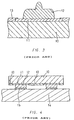
- Fig. 3 is a sectional view showing the electrode structure for the semiconductor device according to the prior art.
- Fig. 4 is a sectional view showing the mounted body including the semiconductor device according to the prior art.
- an aluminum electrode 11 is formed on an IC substrate 10.
- a passivation film 13 is formed on the IC substrate 10 so as to cover the peripheral portion of the aluminum electrode 11.
- a bump electrode 12 is formed on the aluminum electrode 11 by a wire bonding method.
- the semiconductor device having the bump electrode 12 is aligned in the face-down state in such a manner that the bump electrode 12 closely comes in contact with a terminal electrode 15 of a circuit board 14, and is provided on the circuit board 14.
- the bump electrode 12 and the terminal electrode 15 are fused together by thermo-compression bonding or ultrasonic welding. Thus, a mounted body including the semiconductor device is obtained.
- the semiconductor device having the above-mentioned electrode structure and the mounted body including the semiconductor device have the following problems.
- the aluminum electrode is exposed around the bump electrode. For this reason, if water exists in the exposed aluminum electrode portion, there is a possibility that aluminum flows out in a comparatively short time so that the semiconductor device is not electrically connected to the circuit board. In order to enhance the reliability of a junction, it has been proposed to fill a gap between the semiconductor device and the circuit board with an insulating resin. In this case, however, there is a possibility that impurity ions such as chlorine contained in the insulating resin promote the corrosion of the aluminum electrode so that the semiconductor device is not electrically conducted to the circuit board. In the case where an organic board such as a glass epoxy board is used for light weight and low cost, the corrosion of the aluminum electrode becomes more serious because the organic board is generally permeable to water and a lot of impurity ions are present in the organic board.
- DE-A1-43 03 401 discloses a method for forming an electrode structure for a semiconductor device. Thereby, a bump electrode is formed on an aluminum electrode, and onto the aluminium electrode an aluminum oxide film is formed as an passive film.
- Patent abstracts of Japan 7 (115, E - 176) relates to a semiconductor device wherein an oxidized aluminium film is formed over the surface except a region connected with a bonding wire.
- Patent abstracts of Japan 15 (213, E - 1073) discloses a method for forming an electrode structure on a semiconductor device wherein after connecting by a bonding wire, the semiconductor substrate is oxidized and exposed aluminum turns to aluminum oxide.
- the present invention provides a method for forming an electrode structure for a semiconductor device which is suitable for mounting on a circuit board in the face-down state, comprising a bump electrode formed on an aluminum electrode of the semiconductor device; and an aluminum oxide film sufficient for the prevention of corrosion of the aluminum electrode, which is formed on a surface of the aluminum electrode exposed around the bump electrode.
- the aluminum electrode is not corroded due to water and impurity ions when mounting the semiconductor device on the circuit board.
- the aluminum oxide film for the prevention of corrosion should be obtained by further oxidizing a natural oxide film on the surface of the aluminum electrode.
- the thickness of the aluminum oxide film should be 5 to 20 % of the thickness of the aluminum electrode. According to the preferred example, a practical electrode structure for the semiconductor device can be obtained. In other words, the thickness of the aluminum oxide film which is smaller than 5 % of the thickness of the aluminum electrode is not practical because it is very hard to form the aluminum oxide film densely. Furthermore, the thickness of the aluminum oxide film which is greater than 20 % of the thickness of the aluminum electrode is not practical because the resistance value of the aluminum electrode portion is increased too much.
- the thickness of the aluminum oxide film should be 0.05 to 0.2 ⁇ m. According to the preferred example, a practical electrode structure for the semiconductor device can be obtained. In general, the thickness of the aluminum electrode is about 1 ⁇ m. Consequently, the aluminum oxide film having a thickness of 5 to 20 % of the thickness of the aluminum electrode can be obtained.
- the bump electrode should be made of Au.
- the surface of the bump electrode is not oxidized at the step of forming an oxide film on the aluminum electrode of the semiconductor device. Accordingly, the bump electrode made of Au is convenient for the following bonding step. The reason is that if an oxide film is formed between the bonding layer and the surface of the bump electrode, a good electrical conduction cannot be obtained.
- the bump electrode should be formed by a wire bonding method using a Au wire.
- the bump electrode is formed by the wire bonding method in the following manner. First of all, the tip of the Au wire is fused by thermal energy to form a Au ball. Then, the Au ball formed on the tip of the Au wire is put on the aluminum electrode. Thereafter, a pressure of about 50 g is applied to the Au ball formed on the tip of the Au wire at a temperature of about 150°C so as to be bonded onto the aluminum electrode by pressure. Finally, the Au wire is pulled upward. After the above-mentioned steps, the bump electrode made of Au is formed on the aluminum electrode. According to the preferred example, the bump electrode can be formed directly on the aluminum electrode (a general electrode material) of the semiconductor device. Consequently, the bump electrode can be formed easily on the general purpose semiconductor device.
- the aluminum oxide film should be formed by exposing the semiconductor device having the bump electrode formed thereon to the high-temperature state.
- the aluminum oxide film can be formed efficiently in a short time.
- the high-temperature state should have a temperature of 200 to 300°C.
- this temperature range does not have a bad influence on the semiconductor device itself, that is, disconnection of an internal wiring or the like. Consequently, the aluminum oxide film can be formed efficiently in a short time.
- the aluminum oxide film is formed simultaneously with the step of forming the bump electrode at a temperature of 200 to 300°C. According to the invention, the steps of forming the electrode structure for the semiconductor device can be simplified.
- the aluminum oxide film should be formed by immersing the semiconductor device having the bump electrode formed thereon in ammonium persulfate or hydrogen peroxide. According to this preferred example, the aluminum oxide film also can be formed efficiently in a short time.
- a mounted body including a semiconductor device formed by the inventive method, comprising a circuit board having a terminal electrode and a semiconductor device mounted on the circuit board in the face-down state, a bump electrode formed on an aluminum electrode of the semiconductor device and an aluminum oxide film sufficient for the prevention of corrosion that is formed on the surface of the aluminum electrode exposed around the bump electrode, the bump electrode being electrically connected to the terminal electrode on the circuit board through a bonding layer.
- the present mounted body including a semiconductor device the aluminum electrode is not corroded due to water and impurity ions. As a result, there is no possibility that the semiconductor is not electrically conducted to the circuit board. Consequently, a mounted body including a semiconductor device having high reliability can be obtained.
- the circuit board should be formed from a board including an organic material.
- a board containing an organic material such as a glass epoxy board, a paper phenol board or the like has been used as a circuit board for light weight and low cost.
- This kind of board is permeable to water and contains a lot of impurity ions therein.
- the aluminum oxide film for the prevention of corrosion is formed on the surface of the aluminum electrode that is exposed around the bump electrode. Consequently, the aluminum electrode is not corroded due to water and impurity ions. According to the preferred example, it is possible to prevent the corrosion of the aluminum electrode while obtaining a reduction in weight and cost of the semiconductor device.
- the aluminum oxide film for the prevention of corrosion should be obtained by further oxidizing a natural oxide film on the surface of the aluminum electrode.
- the bonding layer should be made of a conductive adhesive.
- the conductive adhesive is obtained by mixing an organic binder, which contributes to adhesion, and a conductive filler, which contributes to electric conduction.
- An epoxy resin, a polyimide resin and the like are used as the organic binder.
- Ag, Cu, Au, Pd, Ni and the like having a mean volume particle diameter of 2 to 5 ⁇ m are used as a conductive filler.
- the content of the conductive filler is 60 to 70 % by weight.
- An amine hardening agent or a phenol hardening agent is used.
- the content of the conductive filler is 60 to 90 % by weight and the hardening temperature is about 200°C.
- the thermal stress on the junction caused by the mismatching of physical property values (in particular, coefficients of thermal expansion) of the semiconductor device and the circuit board is relaxed.
- the mounted body including the semiconductor device can be obtained with high reliability.
- the conductive adhesive has excellent relaxation ability in stress because it is generally softer than an inorganic material such as a solder.
- the bonding layer should be made of a solder.
- the semiconductor device can be mounted at the same steps as the mounting of parts other than the semiconductor device, for example, a chip resistor, a chip capacitor and the like.
- the semiconductor device can also be mounted at the reflow soldering step together with other parts than the semiconductor device. Consequently, the process can be simplified.
- a gap between the semiconductor device and the circuit board should be filled with an insulating resin.
- An example of the insulating resin is an epoxy resin.
- the junction of the semiconductor device and the semiconductor device itself can be protected. In particular, the influence of water under high humidity conditions, such as the degradation of the junction or the failure of the semiconductor device, can be eliminated.
- the thickness of the aluminum oxide film should be 5 to 20 % of the thickness of the aluminum electrode.
- the thickness of the aluminum oxide film should be 0.05 to 0.2 ⁇ m.
- the bump electrode should be made of Au.
- the present invention provides a method for forming an electrode structure of a semiconductor device suitable for mounting on a circuit board, comprising an aluminum electrode; a bump electrode formed on the aluminum electrode; and an aluminum oxide film sufficient for the prevention of corrosion of the aluminum electrode, which is formed on a surface of the aluminum electrode exposed around the bump electrode.
- the aluminum electrode is not corroded due to water and impurity ions after mounting the semiconductor device on the circuit board.
- the semiconductor device in which the aluminum oxide film is formed on the surface of the aluminum electrode is obtained.
- the aluminum electrode is not corroded due to water and impurity ions after mounting the semiconductor device on the circuit board.
- the aluminum electrode is not corroded due to water and impurity ions.
- possibility that the semiconductor device is not electrically conducted to the circuit board is greatly reduced. Consequently, it is possible to obtain the mounted body including the semiconductor device which is very stable and reliable.
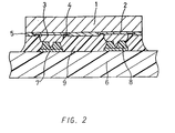
- an aluminum electrode 2 is formed on an IC substrate 1.
- a passivation film 5 made of SiO 2 is formed on the IC substrate 1 so as to cover the peripheral portion of the aluminum electrode 2.
- a bump electrode 3 is formed on the aluminum electrode 2 by a wire bonding method.
- the aluminum electrode 2 has an aluminum oxide film 4 formed on the surface which is exposed around the bump electrode 3. If the aluminum oxide film 4 is formed on the surface of the aluminum electrode 2 that is exposed around the bump electrode 3, the aluminum electrode 2 that is not corroded due to water and impurity ions when the semiconductor device is mounted on the circuit board.
- the bump electrode 3 is generally formed by the wire bonding method at a comparatively low temperature of about 150°C.
- the IC substrate 1 having about 100 aluminum electrodes 2 only passes through a heat history at a temperature of 150°C for a very short time of about 10 secs. For this reason, a natural oxide film formed on the surface of the aluminum electrode 2 during wire bonding has a thickness of about 0.01 ⁇ m and is porous, and is not sufficient to prevent the corrosion of the aluminum electrode 2.
- the thickness of the aluminum oxide film 4 should be 5 to 20 % of the thickness of the aluminum electrode 2.
- the thickness of the aluminum electrode 2 of the semiconductor device is about 1 ⁇ m. In this case, it is sufficient that the thickness of the aluminum oxide film 4 is about 0.1 ⁇ m. If the aluminum oxide film 4 is dense (there is no pin hole), the thickness of the aluminum oxide film 4 may be smaller, that is, about 0.05 ⁇ m.
- the thickness of the aluminum oxide film 4 which is smaller than 5 % of the thickness of the aluminum electrode 2, that is, 0.05 ⁇ m, is not practical because it is very hard to form the aluminum oxide film 4 densely.
- the thickness of the aluminum oxide film 4 which is greater than 20 % of the thickness of the aluminum electrode 2, that is, 0.2 ⁇ m is not practical because the resistance value of the aluminum electrode portion is increased too much.
- the aluminum oxide film 4 can be formed by exposing the IC substrate 1 having the bump electrode 3 provided thereon to the high-temperature state (for example, 300°C) in the air. More specifically, the aluminum oxide film 4 can be formed by a thermal oxidation method. Thus, the aluminum oxide film 4 can be formed efficiently in a short time by using the thermal oxidation method. In this case, it is preferable that the high-temperature state should have a temperature of 200 to 300°C.
- the bump electrode 3 should be made of Au.
- the bump electrode 3 made of Au is convenient for the following bonding step because the surface of the bump electrode 3 is not oxidized at the step of forming an oxide film on the aluminum electrode 2. This is important because if an oxide film is formed between the bonding layer and the surface of the bump electrode 3, a good electric conduction cannot be obtained.
- the bump electrode 3 can be directly formed on the aluminum electrode (a general electrode material) 2 by the wire bonding method using a Au wire in the same manner as in the present embodiment. Consequently, the bump electrode can be easily formed on a general purpose semiconductor device.
- the bump electrode is formed by a plating method. In this case, a thin film such as an adherence layer or a diffusion preventive layer is formed on the aluminum electrode and the bump electrode is then formed on the thin film. For this reason, the complicated process and apparatus are required.
- the tip of the Au wire is fused by thermal energy to form a Au ball.
- the Au ball formed on the tip of the Au wire is put on the aluminum electrode.
- a pressure of about 50 g is applied to the Au ball formed on the tip of the Au wire at a temperature of about 150°C so as to be bonded onto the aluminum electrode by pressure.
- the Au wire is pulled upward.
- the bump electrode 3 made of Au is formed on the aluminum electrode 2.
- the bump electrode 3 can be formed on the aluminum electrode 2 and the aluminum oxide film 4 can be formed on the surface of the aluminum electrode 2 that is exposed around the bump electrode 3.
- the bump electrode 3 and the aluminum oxide film 4 are formed at the same time, therefore the step of forming the electrode structure for the semiconductor device can be simplified.
- a conductive adhesive 8 is applied as a bonding layer to the tip portion of the bump electrode 3 of the semiconductor device having the above-mentioned structure by a transfer method or a printing method. Then, the semiconductor device is aligned in the face-down state in such a manner that the bump electrode 3 abuts on the terminal electrode 7 of the circuit board 6. Then, the semiconductor device is mounted on the circuit board 6.
- the conductive adhesive 8 is hardened in this state, the IC substrate 1 can be electrically connected to the circuit board 6.
- a gap between the IC substrate 1 and the circuit board 6 is filled with an insulating resin 9 such as an epoxy resin so that the mounted body including the semiconductor device can be obtained.
- an insulating resin 9 such as an epoxy resin
- the junction between the board and the IC substrate 1 and the IC substrate 1 itself can be protected.
- the above-mentioned IC substrate 1 that is, the IC substrate 1 in which the surface is exposed around the bump electrode 3, is used and has the aluminum oxide film 4 formed thereon.
- the aluminum electrode 2 is not corroded due to water and impurity ions.
- the IC substrate 1 is not electrically connected to the circuit board 6. Consequently, it is possible to obtain the mounted body including the semiconductor device with high reliability.
- the circuit board 6 an organic board such as a glass epoxy board which is permeable to water and contains a lot of impurity ions. Consequently, the weight and size of the semiconductor device can be reduced.
- An epoxy resin which is generally used as the insulating resin 9 is closely bonded to the metal surface by causing a hydroxyl group in the resin to generate hydrogen bonding with an oxide on the metal surface.
- the adhesion strength on an interface between the insulating resin 9 and the aluminum electrode 2 is enhanced.
- the sealing effect of the insulating resin 9 can be enhanced still more.
- the conductive adhesive 8 is used as a bonding layer, the thermal stress on the junction caused by the mismatching of physical property values (in particular, coefficients of thermal expansion) of the IC substrate 1 with the circuit board 6 is relaxed so that the mounted body including the semiconductor device can be obtained with high reliability.
- the reason is that the conductive adhesive has excellent relaxation ability in stress because it is softer than an inorganic material such as a solder.
- the conductive adhesive is obtained by mixing an organic binder which contributes to adhesion with a conductive filler which contributes to electric conduction. An epoxy resin, a polyimide resin and the like are used as the organic binder.
- the conductive filler Ag, Cu, Au, Pd, Ni and the like which have a mean volume particle diameter of 2 to 5 ⁇ m are used as the conductive filler. If the epoxy resin is used for the organic binder, the content of the conductive filler is 60 to 70 % by weight and amine and phenol hardening agents are used. If the polyimide resin is used as the organic binder, the content of the conductive filler is 60 to 90 % by weight and the hardening temperature is about 200°C.
- the bump electrode 3 is formed by the wire bonding method, which should not be construed as being restricted. If the bump electrode 3 is directly formed on the aluminum electrode 2, an electroless plating method may be used.
- the conductive adhesive 8 is formed as the bonding layer on the bump electrode 3 by the transfer method or the printing method, the bonding layer instead may be formed on the terminal electrode 7 of the circuit board 6 in advance.
- the conductive adhesive 8 is used as the bonding layer in the present embodiment
- other bonding materials such as a solder may be used.
- the semiconductor device can be mounted at the same steps as the mounting of parts other than the semiconductor device, for example, a chip resistor, a chip capacitor and the like. As a result, the semiconductor device can collectively be mounted at the reflow soldering step together with parts other than the semiconductor device. Consequently, the process can be simplified.
- the aluminum oxide film 4 is formed by the thermal oxidation method in the inventive embodiment, another method for oxidizing the surface of the aluminum electrode 2 may be used.
- the semiconductor device having the bump electrode 3 formed thereon is immersed in ammonium persulfate or hydrogen peroxide so as to form the aluminum oxide film 4.
Applications Claiming Priority (2)
| Application Number | Priority Date | Filing Date | Title |
|---|---|---|---|
| JP17838695 | 1995-07-14 | ||
| JP178386/95 | 1995-07-14 |
Publications (3)
| Publication Number | Publication Date |
|---|---|
| EP0753890A2 EP0753890A2 (en) | 1997-01-15 |
| EP0753890A3 EP0753890A3 (en) | 1997-03-05 |
| EP0753890B1 true EP0753890B1 (en) | 1999-06-02 |
Family
ID=16047590
Family Applications (1)
| Application Number | Title | Priority Date | Filing Date |
|---|---|---|---|
| EP96111379A Expired - Lifetime EP0753890B1 (en) | 1995-07-14 | 1996-07-15 | Method of forming an electrode structure for a semiconductor device |
Country Status (8)
| Country | Link |
|---|---|
| US (2) | US6387794B2 (zh) |
| EP (1) | EP0753890B1 (zh) |
| KR (1) | KR100236448B1 (zh) |
| CN (1) | CN1107979C (zh) |
| DE (1) | DE69602686T2 (zh) |
| MY (1) | MY118453A (zh) |
| SG (1) | SG54349A1 (zh) |
| TW (1) | TW318321B (zh) |
Families Citing this family (30)
| Publication number | Priority date | Publication date | Assignee | Title |
|---|---|---|---|---|
| JP3030271B2 (ja) | 1997-05-19 | 2000-04-10 | 富士通株式会社 | 半導体部品の実装方法 |
| DE69811296D1 (de) * | 1997-07-11 | 2003-03-20 | Bosch Gmbh Robert | Erhöhte Haftung der Unterseitenbeschichtung von Flip-Chips |
| JP3421548B2 (ja) | 1997-09-10 | 2003-06-30 | 富士通株式会社 | 半導体ベアチップ、半導体ベアチップの製造方法、及び半導体ベアチップの実装構造 |
| TW451535B (en) * | 1998-09-04 | 2001-08-21 | Sony Corp | Semiconductor device and package, and fabrication method thereof |
| JP3399518B2 (ja) * | 1999-03-03 | 2003-04-21 | インターナショナル・ビジネス・マシーンズ・コーポレーション | 半導体構造およびその製造方法 |
| JP3526788B2 (ja) | 1999-07-01 | 2004-05-17 | 沖電気工業株式会社 | 半導体装置の製造方法 |
| JP4722318B2 (ja) * | 2000-06-05 | 2011-07-13 | ローム株式会社 | チップ抵抗器 |
| US7084716B2 (en) | 2001-04-10 | 2006-08-01 | Picosecond Pulse Labs | Ultrafast sampler with coaxial transition |
| US6900710B2 (en) | 2001-04-10 | 2005-05-31 | Picosecond Pulse Labs | Ultrafast sampler with non-parallel shockline |
| US20030116346A1 (en) * | 2001-12-21 | 2003-06-26 | Forster James Allam | Low cost area array probe for circuits having solder-ball contacts are manufactured using a wire bonding machine |
| US20040007779A1 (en) * | 2002-07-15 | 2004-01-15 | Diane Arbuthnot | Wafer-level method for fine-pitch, high aspect ratio chip interconnect |
| US7358834B1 (en) | 2002-08-29 | 2008-04-15 | Picosecond Pulse Labs | Transmission line voltage controlled nonlinear signal processors |
| US7646095B2 (en) * | 2003-09-30 | 2010-01-12 | Panasonic Corporation | Semiconductor device |
| US7351656B2 (en) * | 2005-01-21 | 2008-04-01 | Kabushiki Kaihsa Toshiba | Semiconductor device having oxidized metal film and manufacture method of the same |
| JP2007053130A (ja) * | 2005-08-15 | 2007-03-01 | Matsushita Electric Ind Co Ltd | 接合構造および接合方法 |
| US20070045812A1 (en) * | 2005-08-31 | 2007-03-01 | Micron Technology, Inc. | Microfeature assemblies including interconnect structures and methods for forming such interconnect structures |
| US7612629B2 (en) | 2006-05-26 | 2009-11-03 | Picosecond Pulse Labs | Biased nonlinear transmission line comb generators |
| US20080005204A1 (en) * | 2006-06-30 | 2008-01-03 | Scientific-Atlanta, Inc. | Systems and Methods for Applying Retention Rules |
| US7700475B1 (en) * | 2006-10-05 | 2010-04-20 | Marvell International Ltd. | Pillar structure on bump pad |
| KR100811034B1 (ko) * | 2007-04-30 | 2008-03-06 | 삼성전기주식회사 | 전자소자 내장 인쇄회로기판의 제조방법 |
| JP4431606B2 (ja) * | 2007-10-05 | 2010-03-17 | シャープ株式会社 | 半導体装置、半導体装置の実装方法、および半導体装置の実装構造 |
| US8570239B2 (en) * | 2008-10-10 | 2013-10-29 | LHC2 Inc. | Spiraling surface antenna |
| TW201133745A (en) * | 2009-08-27 | 2011-10-01 | Advanpack Solutions Private Ltd | Stacked bump interconnection structure and semiconductor package formed using the same |
| JP5303489B2 (ja) * | 2010-02-16 | 2013-10-02 | ルネサスエレクトロニクス株式会社 | 半導体装置の製造方法 |
| US8927391B2 (en) * | 2011-05-27 | 2015-01-06 | Taiwan Semiconductor Manufacturing Company, Ltd. | Package-on-package process for applying molding compound |
| US9105552B2 (en) * | 2011-10-31 | 2015-08-11 | Taiwan Semiconductor Manufacturing Company, Ltd. | Package on package devices and methods of packaging semiconductor dies |
| CN102672340B (zh) * | 2012-05-29 | 2014-08-06 | 李光 | 直接在铝材上进行金丝球超声波焊接工艺 |
| CN103907180B (zh) * | 2012-08-24 | 2016-08-31 | 日本特殊陶业株式会社 | 布线基板 |
| TWI536508B (zh) | 2012-08-24 | 2016-06-01 | Ngk Spark Plug Co | Wiring board |
| CN108109980A (zh) * | 2017-12-01 | 2018-06-01 | 中芯长电半导体(江阴)有限公司 | 芯片尺寸封装结构及其制备方法 |
Family Cites Families (28)
| Publication number | Priority date | Publication date | Assignee | Title |
|---|---|---|---|---|
| US3629669A (en) | 1968-11-25 | 1971-12-21 | Gen Motors Corp | Passivated wire-bonded semiconductor device |
| JPS4952973A (zh) | 1972-09-22 | 1974-05-23 | ||
| US4258382A (en) | 1978-07-03 | 1981-03-24 | National Semiconductor Corporation | Expanded pad structure |
| JPS5827334A (ja) * | 1981-08-11 | 1983-02-18 | Nippon Telegr & Teleph Corp <Ntt> | 半導体装置 |
| JPS5833848A (ja) * | 1981-08-24 | 1983-02-28 | Toshiba Corp | 半導体装置 |
| JPS58184728A (ja) * | 1982-04-22 | 1983-10-28 | Tdk Corp | 半導体素子とその製造法 |
| JPS58197736A (ja) | 1982-05-13 | 1983-11-17 | Nec Corp | 半導体装置 |
| JPS59161852A (ja) | 1983-03-04 | 1984-09-12 | Nec Corp | 半導体装置 |
| JPS63236339A (ja) | 1987-03-24 | 1988-10-03 | Nec Corp | 半導体集積回路装置 |
| JPS63269541A (ja) * | 1987-04-27 | 1988-11-07 | Nec Corp | 半導体装置 |
| US5014111A (en) * | 1987-12-08 | 1991-05-07 | Matsushita Electric Industrial Co., Ltd. | Electrical contact bump and a package provided with the same |
| JPH0221622A (ja) | 1988-07-08 | 1990-01-24 | Nec Corp | 半導体装置 |
| JPH0682704B2 (ja) | 1989-06-27 | 1994-10-19 | 株式会社東芝 | 半導体装置 |
| JPH0360035A (ja) * | 1989-07-27 | 1991-03-15 | Nec Corp | 半導体装置 |
| US5074947A (en) * | 1989-12-18 | 1991-12-24 | Epoxy Technology, Inc. | Flip chip technology using electrically conductive polymers and dielectrics |
| JPH03191527A (ja) | 1989-12-20 | 1991-08-21 | Nec Corp | 半導体素子の電極構造 |
| JPH03208354A (ja) * | 1990-01-10 | 1991-09-11 | Mitsubishi Electric Corp | 半導体装置およびその製造方法 |
| JPH03295247A (ja) * | 1990-04-12 | 1991-12-26 | Fujitsu Ltd | 半導体装置の製造方法 |
| JP2563652B2 (ja) | 1990-07-17 | 1996-12-11 | 株式会社東芝 | 半導体装置及びその製造方法 |
| JPH04124880A (ja) | 1990-09-17 | 1992-04-24 | Hitachi Ltd | 半導体式圧力センサ |
| US5136365A (en) * | 1990-09-27 | 1992-08-04 | Motorola, Inc. | Anisotropic conductive adhesive and encapsulant material |
| JPH04214642A (ja) | 1990-12-12 | 1992-08-05 | Mitsubishi Electric Corp | 樹脂封止型半導体装置 |
| JP2731040B2 (ja) | 1991-02-05 | 1998-03-25 | 三菱電機株式会社 | 半導体装置の製造方法 |
| US5565378A (en) * | 1992-02-17 | 1996-10-15 | Mitsubishi Denki Kabushiki Kaisha | Process of passivating a semiconductor device bonding pad by immersion in O2 or O3 solution |
| US5261593A (en) * | 1992-08-19 | 1993-11-16 | Sheldahl, Inc. | Direct application of unpackaged integrated circuit to flexible printed circuit |
| US5436503A (en) | 1992-11-18 | 1995-07-25 | Matsushita Electronics Corporation | Semiconductor device and method of manufacturing the same |
| US5508561A (en) | 1993-11-15 | 1996-04-16 | Nec Corporation | Apparatus for forming a double-bump structure used for flip-chip mounting |
| JP2687856B2 (ja) * | 1993-12-17 | 1997-12-08 | 日本電気株式会社 | バンプの製造方法及び製造装置 |
-
1996
- 1996-07-12 CN CN96109913A patent/CN1107979C/zh not_active Expired - Fee Related
- 1996-07-12 TW TW085108468A patent/TW318321B/zh active
- 1996-07-13 SG SG1996010262A patent/SG54349A1/en unknown
- 1996-07-13 MY MYPI96002895A patent/MY118453A/en unknown
- 1996-07-13 KR KR1019960028350A patent/KR100236448B1/ko not_active IP Right Cessation
- 1996-07-15 EP EP96111379A patent/EP0753890B1/en not_active Expired - Lifetime
- 1996-07-15 DE DE69602686T patent/DE69602686T2/de not_active Expired - Lifetime
-
1998
- 1998-11-19 US US09/197,334 patent/US6387794B2/en not_active Expired - Lifetime
-
2002
- 2002-02-27 US US10/086,210 patent/US6603207B2/en not_active Expired - Lifetime
Also Published As
| Publication number | Publication date |
|---|---|
| US20010014523A1 (en) | 2001-08-16 |
| KR970008446A (ko) | 1997-02-24 |
| KR100236448B1 (ko) | 1999-12-15 |
| DE69602686T2 (de) | 1999-10-21 |
| US6603207B2 (en) | 2003-08-05 |
| SG54349A1 (en) | 1998-11-16 |
| EP0753890A2 (en) | 1997-01-15 |
| EP0753890A3 (en) | 1997-03-05 |
| CN1107979C (zh) | 2003-05-07 |
| CN1147150A (zh) | 1997-04-09 |
| TW318321B (zh) | 1997-10-21 |
| US6387794B2 (en) | 2002-05-14 |
| DE69602686D1 (de) | 1999-07-08 |
| MY118453A (en) | 2004-11-30 |
| US20020081830A1 (en) | 2002-06-27 |
Similar Documents
| Publication | Publication Date | Title |
|---|---|---|
| EP0753890B1 (en) | Method of forming an electrode structure for a semiconductor device | |
| US6103551A (en) | Semiconductor unit and method for manufacturing the same | |
| JP3648277B2 (ja) | 半導体装置 | |
| US6175151B1 (en) | Film carrier tape, semiconductor assembly, semiconductor device, and method of manufacturing the same, mounted board, and electronic instrument | |
| JP3704864B2 (ja) | 半導体素子の実装構造 | |
| KR100272399B1 (ko) | 전자부품의 제조방법 및 이에 의해 제조된 전자부품 | |
| US7374969B2 (en) | Semiconductor package with conductive molding compound and manufacturing method thereof | |
| US6118183A (en) | Semiconductor device, manufacturing method thereof, and insulating substrate for same | |
| KR20000011717A (ko) | 반도체장치의제조방법 | |
| KR20030067590A (ko) | 반도체소자와 그 제조방법 및 반도체장치와 그 제조방법 | |
| US6887778B2 (en) | Semiconductor device and manufacturing method | |
| US6781221B2 (en) | Packaging substrate for electronic elements and electronic device having packaged structure | |
| JP3356649B2 (ja) | 半導体装置及びその製造方法 | |
| JP4416876B2 (ja) | 半導体チップ及び半導体チップの製造方法 | |
| JP3116926B2 (ja) | パッケージ構造並びに半導体装置、パッケージ製造方法及び半導体装置製造方法 | |
| US20080293236A1 (en) | Method of manufacturing chip integrated substrate | |
| JP3012809B2 (ja) | 半導体装置の電極構造体の形成方法 | |
| JP3836449B2 (ja) | 半導体装置の製造方法 | |
| JP3795628B2 (ja) | 半導体チップを搭載する配線基板の製造方法 | |
| JPH09232506A (ja) | 半導体装置およびその製造方法 | |
| JP4440494B2 (ja) | 半導体装置の製造方法 | |
| JP2003086620A (ja) | 突起電極を有する半導体装置及びその製造方法 | |
| JPH0831871A (ja) | 電子部品を表面実装する際に使用する界面封止用フィルム、及び電子部品の表面実装構造 | |
| JP2914569B1 (ja) | 半導体素子の実装方法とその実装体 | |
| JP3951903B2 (ja) | 半導体装置及び半導体装置実装体の製造方法 |
Legal Events
| Date | Code | Title | Description |
|---|---|---|---|
| PUAI | Public reference made under article 153(3) epc to a published international application that has entered the european phase |
Free format text: ORIGINAL CODE: 0009012 |
|
| AK | Designated contracting states |
Kind code of ref document: A2 Designated state(s): DE FR GB NL |
|
| PUAL | Search report despatched |
Free format text: ORIGINAL CODE: 0009013 |
|
| AK | Designated contracting states |
Kind code of ref document: A3 Designated state(s): DE FR GB NL |
|
| 17P | Request for examination filed |
Effective date: 19970410 |
|
| 17Q | First examination report despatched |
Effective date: 19970704 |
|
| GRAG | Despatch of communication of intention to grant |
Free format text: ORIGINAL CODE: EPIDOS AGRA |
|
| GRAG | Despatch of communication of intention to grant |
Free format text: ORIGINAL CODE: EPIDOS AGRA |
|
| GRAG | Despatch of communication of intention to grant |
Free format text: ORIGINAL CODE: EPIDOS AGRA |
|
| GRAH | Despatch of communication of intention to grant a patent |
Free format text: ORIGINAL CODE: EPIDOS IGRA |
|
| GRAH | Despatch of communication of intention to grant a patent |
Free format text: ORIGINAL CODE: EPIDOS IGRA |
|
| GRAA | (expected) grant |
Free format text: ORIGINAL CODE: 0009210 |
|
| RAP1 | Party data changed (applicant data changed or rights of an application transferred) |
Owner name: MATSUSHITA ELECTRIC INDUSTRIAL CO., LTD. |
|
| AK | Designated contracting states |
Kind code of ref document: B1 Designated state(s): DE FR GB NL |
|
| REF | Corresponds to: |
Ref document number: 69602686 Country of ref document: DE Date of ref document: 19990708 |
|
| ET | Fr: translation filed | ||
| PLBE | No opposition filed within time limit |
Free format text: ORIGINAL CODE: 0009261 |
|
| STAA | Information on the status of an ep patent application or granted ep patent |
Free format text: STATUS: NO OPPOSITION FILED WITHIN TIME LIMIT |
|
| 26N | No opposition filed | ||
| REG | Reference to a national code |
Ref country code: GB Ref legal event code: IF02 |
|
| PGFP | Annual fee paid to national office [announced via postgrant information from national office to epo] |
Ref country code: NL Payment date: 20100716 Year of fee payment: 15 |
|
| PGFP | Annual fee paid to national office [announced via postgrant information from national office to epo] |
Ref country code: FR Payment date: 20100805 Year of fee payment: 15 Ref country code: DE Payment date: 20100707 Year of fee payment: 15 |
|
| PGFP | Annual fee paid to national office [announced via postgrant information from national office to epo] |
Ref country code: GB Payment date: 20100714 Year of fee payment: 15 |
|
| REG | Reference to a national code |
Ref country code: NL Ref legal event code: V1 Effective date: 20120201 |
|
| GBPC | Gb: european patent ceased through non-payment of renewal fee |
Effective date: 20110715 |
|
| REG | Reference to a national code |
Ref country code: FR Ref legal event code: ST Effective date: 20120330 |
|
| PG25 | Lapsed in a contracting state [announced via postgrant information from national office to epo] |
Ref country code: DE Free format text: LAPSE BECAUSE OF NON-PAYMENT OF DUE FEES Effective date: 20120201 Ref country code: FR Free format text: LAPSE BECAUSE OF NON-PAYMENT OF DUE FEES Effective date: 20110801 |
|
| PG25 | Lapsed in a contracting state [announced via postgrant information from national office to epo] |
Ref country code: NL Free format text: LAPSE BECAUSE OF NON-PAYMENT OF DUE FEES Effective date: 20120201 |
|
| REG | Reference to a national code |
Ref country code: DE Ref legal event code: R119 Ref document number: 69602686 Country of ref document: DE Effective date: 20120201 |
|
| PG25 | Lapsed in a contracting state [announced via postgrant information from national office to epo] |
Ref country code: GB Free format text: LAPSE BECAUSE OF NON-PAYMENT OF DUE FEES Effective date: 20110715 |