EP0620556A2 - Dispositif de mémoire à semi-conducteur comportant un registre pour le maintien d'un signal résultant du test - Google Patents
Dispositif de mémoire à semi-conducteur comportant un registre pour le maintien d'un signal résultant du test Download PDFInfo
- Publication number
- EP0620556A2 EP0620556A2 EP94105415A EP94105415A EP0620556A2 EP 0620556 A2 EP0620556 A2 EP 0620556A2 EP 94105415 A EP94105415 A EP 94105415A EP 94105415 A EP94105415 A EP 94105415A EP 0620556 A2 EP0620556 A2 EP 0620556A2
- Authority
- EP
- European Patent Office
- Prior art keywords
- data
- signal
- register
- circuit
- decision
- Prior art date
- Legal status (The legal status is an assumption and is not a legal conclusion. Google has not performed a legal analysis and makes no representation as to the accuracy of the status listed.)
- Granted
Links
Images


Classifications
-
- G—PHYSICS
- G11—INFORMATION STORAGE
- G11C—STATIC STORES
- G11C29/00—Checking stores for correct operation ; Subsequent repair; Testing stores during standby or offline operation
- G11C29/04—Detection or location of defective memory elements, e.g. cell constructio details, timing of test signals
- G11C29/08—Functional testing, e.g. testing during refresh, power-on self testing [POST] or distributed testing
- G11C29/12—Built-in arrangements for testing, e.g. built-in self testing [BIST] or interconnection details
- G11C29/38—Response verification devices
- G11C29/40—Response verification devices using compression techniques
-
- G—PHYSICS
- G11—INFORMATION STORAGE
- G11C—STATIC STORES
- G11C29/00—Checking stores for correct operation ; Subsequent repair; Testing stores during standby or offline operation
- G11C29/04—Detection or location of defective memory elements, e.g. cell constructio details, timing of test signals
- G11C29/08—Functional testing, e.g. testing during refresh, power-on self testing [POST] or distributed testing
- G11C29/12—Built-in arrangements for testing, e.g. built-in self testing [BIST] or interconnection details
- G11C29/44—Indication or identification of errors, e.g. for repair
-
- G—PHYSICS
- G11—INFORMATION STORAGE
- G11C—STATIC STORES
- G11C29/00—Checking stores for correct operation ; Subsequent repair; Testing stores during standby or offline operation
- G11C29/04—Detection or location of defective memory elements, e.g. cell constructio details, timing of test signals
- G11C29/08—Functional testing, e.g. testing during refresh, power-on self testing [POST] or distributed testing
- G11C29/12—Built-in arrangements for testing, e.g. built-in self testing [BIST] or interconnection details
- G11C29/46—Test trigger logic
Definitions
- the present invention relates to a semiconductor device and, more particularly, to a semiconductor memory device capable of executing data write and read test operation on a plurality of bits in parallel to one another.
- bit number increase in number of bits or memory cells
- each memory cell is required to be written with test data and the test data is then read out therefrom so that the testing time is increased in proportion to the increase of the bit number of the memories.
- the memory capacity has been quadrupled in every 3 or 4 years, so that the increase in the testing time has become a problem that cannot be affored to be ignored.
- a semiconductor memory device equipped with a test circuit which is activated during a test mode to write and read test data in and from a plurality of memory cells was proposed as disclosed in ISSCC 85 Digest of Technical Papers, pp. 240-241, titled "A 90ns 1Mb DRAM with Multi-Bit Test Mode". Namely, during the test mode, the test data having logic "1" or "0" is written simultaneously into four memory cells, and the test data thus written are then read out therefrom simultaneously, to detect whether or not the four test data are coincident with one other.
- a noncoincidence detection signal is output as a defective bit detection signal to inform the defectiveness of the memory cell or cells.
- the noncoincidence detection signal is in valid only during one test access operation for four memory cells. For this reason, the defective bit detection signal has to be monitored every one test access operation, i.e., every four memory cells. As a result, while the test time for one memory device is shortened, the total test time for one test board including a plurality of memory devices are not reduced as expected. This will be further described in the following by referring to FIG. 1.
- the testing time is given by m x 9N x M x Tc which leads to a problem that the testing time is too long Moreover, since the test decides whether the read data of plural bits are coincide or not, the read data are decided to be in coincidence even if all of the read data are changed to the same level that are different from the written data. In other words, the method has a problem that the failure in which all bits are inverted cannot be detected.
- the semiconductor memory device comprises a memory circuit capable of writing and reading a plurality of data at the same time, a plurality of write and read data buses connected to the memory circuit, a data write/read circuit which during the test mode writes simultaneously a plurality of data of the same level to predetermined address regions of the memory circuit, and later reads the plurality of data stored in the same addresses, a comparison data register which stores the data identical to the plurality of data written by the data write/read circuit to the memory circuit, a decision circuit which decides whether the plurality of data read from the memory circuit agree entirely with the data stored in the comparison data register, and generates a decision signal of coincidence level or noncoincidence level, a decision result register which is reset by a reset signal generated only once immediately after the device entered the test mode and is set to a set level in response to a noncoincidence level of the decision signal, and holds the state until the next reset signal is generated, and a decision result read circuit which reads the contents of the decision result register.
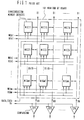
- a memory cell array 2 is a DRAM memory cell array in which memory cells MC are arranged in array at the intersections of a plurality of word lines WL and bit lines BL. Each memory cell is of the so-called one-transistor one-capacitor type. Address signals A0 to An supplied via an address buffer 1 are supplied to a column decoder 20 and a row decoder 21, and memory cells corresponding to the address signals are selected.
- DRAMs dynamic random access memories
- Data buses DB0 to DB3 are operatively coupled to four memory cells of the memory cell array 2 selected by the address.
- a selector 4 is a circuit which selects one of the data buses DB0 to DB3 according to predetermined two bits of the address signals A0 to An when a test mode signal TST is at an inactive level, and selects all of the data buses DB0 to DB3 when the test mode signal TST is at the active level.
- a comparison data register 10 is a register which stores data DC for comparison corresponding to a latch signal LDC.
- a decision circuit 5 decides whether or not read-data of 4 bits supplied from the data buses DB0 to DB3 and data stored in the comparison data register 10 are coincident with one another, and outputs a decision signal JD of coincidence or noncoincidence level.
- a gate circuit 6 outputs a decision signal JD when a gate signal GT is at the active level.
- the gate circuit 6 is provided to prevent malfunction of a decision result register 7 due to a spike noise caused by skew mismatch of the input signal to the decision circuit.
- the decision result register 7 is reset by a register reset signal RST and set to a set level in response to the noncoincidence level of the decision signal transmitted from the gate circuit, and holds the set level until the next generation of the register reset signal RST.
- a selector 8 selectively outputs 1-bit read data output from the selector 4 when the test mode signal TST is at the nonactive level, and selectively outputs a decision result signal RSLT of the decision result register when the test mode signal TST is at the active level.
- a data-in buffer circuit 3 fetches and outputs a 1-bit data supplied to an input and output terminal DI/O in response to the level of a data input signal IN.
- a data-out buffer circuit 9 outputs data selected by the selector 8 to the input and output terminal DI/O in response to the level of a data output signal OUT.
- a control signal generating circuit 11 generates the test mode signal TST, gate signal GT, register reset signal RST, latch signal LDC, output signal OUT and data input signal IN in response to the mutual level relation of a row address strobe signal RASb, column address strobe signal CASb, write enable signal WEb and output enable signal OEb.
- test mode signal TST When the test mode signal TST is at the nonactive level (low level), normal write and read (normal mode) is carried out, and when the test mode signal TST is at the active level (high level), write and read of test data, coincidence decision of data read out and read of the decision result (test mode) are carried out.
- the selector 4 selects one line out of data buses DB0 to DB3 in response to predetermined 2 bits among column address signals fetched to the address buffer circuit 1 (see FIG. 2)
- the data input signal IN of the control signal generating circuit 11 goes to the active level synchronized with the activation (low level) of the write enable signal WEb. Accordingly, the data-in buffer circuit 3 supplies a 1-bit write data to the selector 4.
- the write data is supplied to the memory cell array 2 via one line out of the data buses DB0 to DB3 selected by the selector 4.
- Memory cells are selected by the column decoder 20 and the row decoder 21 corresponding to the input addresses A0 to An, and the write data are stored.
- 1-bit data out of 4-bit data read out in response to the input addresses A0 to An is selected by the selector 4, and it is supplied to the selector 8.
- the selector 8 supplies the 1-bit data read out, supplied by the selector 4 in response to the nonactive level of the test mode signal TST, to the data-out buffer circuit 9. Since the control signal generating circuit 11 sends the data output OUT to the active level in response to the activation (low level) of the output enable signal OEb, the data-out buffer circuit 9 outputs the data read-out to the input and output terminal DI/O.
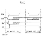
- the test mode operation of this embodiment will be described.
- the control signal generating circuit 11 After execution of the test mode set cycle shown in FIG. 3, if the output enable signal OEb is at the active level (low level) at the time of transition of the row address strobe signal RASb to the active level (low level), as shown in FIG. 4, the control signal generating circuit 11 outputs a register reset signal RST with a predetermined width.
- the decision result register 7 is reset in response to the register reset signal RST.
- the above-mentioned operation represents the register reset cycle which is executed just once immediately after the system entered the test mode.
- a write cycle shown in FIG. 5 and a decision cycle shown in FIG. 6 are executed repeatedly according to a predetermined test pattern (for example, the 9N marching system).
- a predetermined test pattern for example, the 9N marching system.
- the data input signal IN goes to the active level synchronized with the activation (low level) of the write enable signal WEb. Accordingly, the data-in buffer circuit 3 supplies a 1-bit write data to the selector 4. Since the test mode signal TST is at the active level (high level) during the test mode, the selector 4 supplies data of the same level to all of the data buses DB0 to DB3. As a result, data of one set of 4 bits with the same level are written to memory cells corresponding to the input addresses A0 to An.
- the control signal generating circuit 11 generates a latch signal LDC having a predetermined pulse width.
- comparison data DC of the same level as the data written in the write cycle are supplied from the input and output terminal DI/O, and are stored.
- one set of data of 4 bits corresponding to the input addresses A0 to An are read from the memory cell array 2, and are supplied to the decision circuit 5.
- the decision circuit 5 decides whether the comparison data and all of the one set data of 4 bits coincide.
- the decision signal JD having a level corresponding to coincidence or noncoincidence is supplied to the decision result register 7 via the gate circuit 6 in response to the gate signal GT which is generated by detecting the activation level of the signal CASb and the nonactivation of the signal WEb at the time of transition of the signal RASb to the nonactive level.
- the decision result register 7 converts the contents of the decision signal from reset level (PASS) to set level (FAIL) only when it indicates noncoincidence, and holds this state thereafter.
- a decision result signal RSLT showing the reset level (PASS) is output from the decision result register 7.
- the circuit outputs a decision result signal RSLT of the set level (FAIL).
- a decision result output cycle shown in FIG. 7 is executed.
- the decision result output cycle is executed when the signal OEb is brought to the active level after the signal RASb and the signal CASb sequentially made transition to the active level.
- the decision result signal RSLT is output to the input and output terminal DI/O via the selector 8 and the data out buffer 9.
- the decision circuit 5 is detecting coincidence of the data of one set of 4 bits read from the memory cell array 2 and the data stored in the comparison data register, so that it is possible to detect the all-bit inversion failure which was unable to be detected conventionally.
- the write cycle and the decision cycle (of cycle time Tc) are executed repeatedly according to a predetermined test pattern (for example, the 9N marching system). Since the above-mentioned operations are given simultaneously to the m x k semiconductor memory devices, the test results for all the semiconductor memory devices are stored in the decision result register 7 at the completion of the decision cycle. In other words, the test result for all the semiconductor memory devices on the monitor board can be obtained by one time of test.
- the test result for k memories in a row (for example, from MIC11 to MIC1k) is output to the input and output line by starting the decision result output cycle.
- the testing time for this operation is, for the case of the 9N marching system, 9N x M x Tc + mTc + Tc , where M is the total number of 4-bit sets of memories and Tc is the one cycle time (for write and decision).
- mTc in the second term represents the decision result output cycle
- Tc in the third term is the register reset cycle. Since m+1 is very small compared with 9N x M, the last two terms can be neglected. Therefore, the testing time becomes 9N x M x Tc which is 1/m of the conventional testing time.
- This embodiment represents a semiconductor memory device which, in the normal mode, writes different data of 4 bits at the same address in the memory cell array, then reads the data.
- the difference in constitution of this embodiment from that of the first embodiment is that each of the data buses DB0 to DB3 is connected to the corresponding data-in buffer (3a to 3d) and data-out buffer (9a to 9d) without intermediary of a selector (see FIG. 2).
- control signal generating circuit 11 In the aforementioned operations, the operations of the various kinds of control signal or the like supplied by the control signal generating circuit 11 are the same as in the first embodiment.
Applications Claiming Priority (3)
| Application Number | Priority Date | Filing Date | Title |
|---|---|---|---|
| JP5083190A JPH06295599A (ja) | 1993-04-09 | 1993-04-09 | 半導体記憶装置 |
| JP8319093 | 1993-04-09 | ||
| JP83190/93 | 1993-04-09 |
Publications (3)
| Publication Number | Publication Date |
|---|---|
| EP0620556A2 true EP0620556A2 (fr) | 1994-10-19 |
| EP0620556A3 EP0620556A3 (fr) | 1998-01-21 |
| EP0620556B1 EP0620556B1 (fr) | 2001-02-28 |
Family
ID=13795410
Family Applications (1)
| Application Number | Title | Priority Date | Filing Date |
|---|---|---|---|
| EP94105415A Expired - Lifetime EP0620556B1 (fr) | 1993-04-09 | 1994-04-07 | Dispositif de mémoire à semi-conducteur comportant un registre pour le maintien d'un signal résultant du test |
Country Status (5)
| Country | Link |
|---|---|
| US (1) | US5673270A (fr) |
| EP (1) | EP0620556B1 (fr) |
| JP (1) | JPH06295599A (fr) |
| KR (1) | KR0134751B1 (fr) |
| DE (1) | DE69426733T2 (fr) |
Cited By (1)
| Publication number | Priority date | Publication date | Assignee | Title |
|---|---|---|---|---|
| CN106024050A (zh) * | 2015-03-31 | 2016-10-12 | 爱思开海力士有限公司 | 输出状态失败信号的半导体存储器件及其操作方法 |
Families Citing this family (28)
| Publication number | Priority date | Publication date | Assignee | Title |
|---|---|---|---|---|
| JP3547059B2 (ja) * | 1995-06-30 | 2004-07-28 | 株式会社アドバンテスト | 半導体メモリ試験方法およびこの方法を実施する装置 |
| US5983375A (en) * | 1995-12-27 | 1999-11-09 | Samsung Electronics, Co., Ltd. | Multi-bit test circuit and method thereof |
| KR100216993B1 (ko) * | 1997-07-11 | 1999-09-01 | 윤종용 | 병합 데이터 출력모드와 표준동작 모드로 동작하는 집적회로소자를 함께 검사할 수 있는 검사용 기판 |
| US5996097A (en) * | 1997-04-28 | 1999-11-30 | International Business Machines Corporation | Testing logic associated with numerous memory cells in the word or bit dimension in parallel |
| JP3235523B2 (ja) * | 1997-08-06 | 2001-12-04 | 日本電気株式会社 | 半導体集積回路 |
| JP3237579B2 (ja) * | 1997-08-07 | 2001-12-10 | 日本電気株式会社 | メモリテスト回路 |
| KR100281105B1 (ko) * | 1998-02-04 | 2001-02-01 | 김영환 | 디램의 데이타 출력 회로 |
| US5936901A (en) * | 1998-03-19 | 1999-08-10 | Micron Technology, Inc. | Shared data lines for memory write and memory test operations |
| US5982684A (en) * | 1998-05-28 | 1999-11-09 | Intel Corporation | Parallel access testing of a memory array |
| US6324657B1 (en) * | 1998-06-11 | 2001-11-27 | Micron Technology, Inc. | On-clip testing circuit and method for improving testing of integrated circuits |
| JP2000076899A (ja) * | 1998-08-26 | 2000-03-14 | Oki Micro Design:Kk | 半導体記憶装置 |
| US6550023B1 (en) * | 1998-10-19 | 2003-04-15 | Hewlett Packard Development Company, L.P. | On-the-fly memory testing and automatic generation of bitmaps |
| JP3945939B2 (ja) * | 1999-05-31 | 2007-07-18 | 富士通株式会社 | 圧縮テスト可能なメモリ回路 |
| JP2001101895A (ja) | 1999-09-30 | 2001-04-13 | Mitsubishi Electric Corp | 半導体集積回路装置 |
| JP2001202797A (ja) | 2000-01-20 | 2001-07-27 | Mitsubishi Electric Corp | 半導体記憶装置および半導体テスト方法 |
| DE10124923B4 (de) * | 2001-05-21 | 2014-02-06 | Qimonda Ag | Testverfahren zum Testen eines Datenspeichers und Datenspeicher mit integrierter Testdatenkompressionsschaltung |
| ATE384331T1 (de) * | 2001-11-12 | 2008-02-15 | Siemens Ag | Speichertest |
| JP2004198367A (ja) | 2002-12-20 | 2004-07-15 | Fujitsu Ltd | 半導体装置及びその試験方法 |
| US20050149792A1 (en) * | 2002-12-20 | 2005-07-07 | Fujitsu Limited | Semiconductor device and method for testing the same |
| JP4400081B2 (ja) * | 2003-04-08 | 2010-01-20 | エルピーダメモリ株式会社 | 半導体記憶装置 |
| JP2006004475A (ja) * | 2004-06-15 | 2006-01-05 | Toshiba Corp | 半導体集積回路装置 |
| JP2006048748A (ja) * | 2004-07-30 | 2006-02-16 | Renesas Technology Corp | 半導体記憶装置 |
| JP4712365B2 (ja) * | 2004-08-13 | 2011-06-29 | ルネサスエレクトロニクス株式会社 | 不揮発性半導体記憶装置および半導体記憶装置 |
| US20060041798A1 (en) * | 2004-08-23 | 2006-02-23 | On-Chip Technologies, Inc. | Design techniques to increase testing efficiency |
| US7376872B1 (en) | 2004-11-01 | 2008-05-20 | Lattice Semiconductor Corporation | Testing embedded memory in integrated circuits such as programmable logic devices |
| JP5137550B2 (ja) * | 2007-12-12 | 2013-02-06 | キヤノン株式会社 | 情報処理装置及びその制御方法 |
| KR101477603B1 (ko) * | 2013-04-09 | 2014-12-30 | (주)피델릭스 | 입력 테스트 비트 수를 감소하는 반도체 메모리 장치 및 이에 대한 테스트 데이터 기입 방법 |
| KR102485210B1 (ko) * | 2016-08-18 | 2023-01-06 | 에스케이하이닉스 주식회사 | 반도체 메모리 장치 |
Citations (4)
| Publication number | Priority date | Publication date | Assignee | Title |
|---|---|---|---|---|
| EP0092245A2 (fr) * | 1982-04-20 | 1983-10-26 | STMicroelectronics, Inc. | Commande fonctionnelle pour mémoire semi-conductrice |
| JPS6325749A (ja) * | 1986-07-18 | 1988-02-03 | Nec Corp | 半導体記憶素子 |
| DE4023015C1 (fr) * | 1990-06-18 | 1991-12-19 | Samsung Electronics Co., Ltd., Suwon, Kr | |
| JPH0428100A (ja) * | 1990-05-24 | 1992-01-30 | Nec Corp | Rom試験回路 |
Family Cites Families (20)
| Publication number | Priority date | Publication date | Assignee | Title |
|---|---|---|---|---|
| US4503536A (en) * | 1982-09-13 | 1985-03-05 | General Dynamics | Digital circuit unit testing system utilizing signature analysis |
| JPS59185097A (ja) * | 1983-04-04 | 1984-10-20 | Oki Electric Ind Co Ltd | 自己診断機能付メモリ装置 |
| JPS6088370A (ja) * | 1983-10-20 | 1985-05-18 | Toshiba Corp | 論理回路 |
| USRE34445E (en) * | 1985-01-18 | 1993-11-16 | University Of Michigan | Self-testing dynamic RAM |
| US4757503A (en) * | 1985-01-18 | 1988-07-12 | The University Of Michigan | Self-testing dynamic ram |
| JPS6238600A (ja) * | 1985-08-14 | 1987-02-19 | Fujitsu Ltd | 半導体記憶装置 |
| JP2684365B2 (ja) * | 1987-04-24 | 1997-12-03 | 株式会社日立製作所 | 半導体記憶装置 |
| JP2602225B2 (ja) * | 1987-04-24 | 1997-04-23 | 株式会社日立製作所 | ダイナミツクram |
| US5034923A (en) * | 1987-09-10 | 1991-07-23 | Motorola, Inc. | Static RAM with soft defect detection |
| JP2938470B2 (ja) * | 1989-06-01 | 1999-08-23 | 三菱電機株式会社 | 半導体記憶装置 |
| JP2717712B2 (ja) * | 1989-08-18 | 1998-02-25 | 三菱電機株式会社 | 半導体記憶装置 |
| JPH0752597B2 (ja) * | 1989-10-30 | 1995-06-05 | 三菱電機株式会社 | 半導体メモリ装置 |
| KR920005798A (ko) * | 1990-04-18 | 1992-04-03 | 미타 가쓰시게 | 반도체 집적회로 |
| US5265100A (en) * | 1990-07-13 | 1993-11-23 | Sgs-Thomson Microelectronics, Inc. | Semiconductor memory with improved test mode |
| JP2568455B2 (ja) * | 1990-08-16 | 1997-01-08 | 三菱電機株式会社 | 半導体記憶装置 |
| JPH0512900A (ja) * | 1991-06-28 | 1993-01-22 | Nec Corp | テスト機能を有する半導体記憶装置及びそのテスト方法 |
| US5457696A (en) * | 1991-08-08 | 1995-10-10 | Matsushita Electric Industrial Co., Ltd. | Semiconductor memory having internal test circuit |
| JP3049343B2 (ja) * | 1991-11-25 | 2000-06-05 | 安藤電気株式会社 | メモリ試験装置 |
| JPH06203597A (ja) * | 1992-09-25 | 1994-07-22 | Nec Corp | ダイナミックram |
| JP2768175B2 (ja) * | 1992-10-26 | 1998-06-25 | 日本電気株式会社 | 半導体メモリ |
-
1993
- 1993-04-09 JP JP5083190A patent/JPH06295599A/ja active Pending
-
1994
- 1994-04-07 DE DE69426733T patent/DE69426733T2/de not_active Expired - Fee Related
- 1994-04-07 EP EP94105415A patent/EP0620556B1/fr not_active Expired - Lifetime
- 1994-04-08 KR KR1019940007327A patent/KR0134751B1/ko not_active IP Right Cessation
-
1995
- 1995-09-13 US US08/527,761 patent/US5673270A/en not_active Expired - Lifetime
Patent Citations (4)
| Publication number | Priority date | Publication date | Assignee | Title |
|---|---|---|---|---|
| EP0092245A2 (fr) * | 1982-04-20 | 1983-10-26 | STMicroelectronics, Inc. | Commande fonctionnelle pour mémoire semi-conductrice |
| JPS6325749A (ja) * | 1986-07-18 | 1988-02-03 | Nec Corp | 半導体記憶素子 |
| JPH0428100A (ja) * | 1990-05-24 | 1992-01-30 | Nec Corp | Rom試験回路 |
| DE4023015C1 (fr) * | 1990-06-18 | 1991-12-19 | Samsung Electronics Co., Ltd., Suwon, Kr |
Non-Patent Citations (2)
| Title |
|---|
| PATENT ABSTRACTS OF JAPAN vol. 12, no. 233 (P-724), 5 July 1988 & JP 63 025749 A (NEC CO.) * |
| PATENT ABSTRACTS OF JAPAN vol. 16, no. 197 (P-1350), 12 May 1992 & JP 04 028100 A (NEC CO.) * |
Cited By (2)
| Publication number | Priority date | Publication date | Assignee | Title |
|---|---|---|---|---|
| CN106024050A (zh) * | 2015-03-31 | 2016-10-12 | 爱思开海力士有限公司 | 输出状态失败信号的半导体存储器件及其操作方法 |
| CN106024050B (zh) * | 2015-03-31 | 2021-12-07 | 爱思开海力士有限公司 | 输出状态失败信号的半导体存储器件及其操作方法 |
Also Published As
| Publication number | Publication date |
|---|---|
| JPH06295599A (ja) | 1994-10-21 |
| DE69426733D1 (de) | 2001-04-05 |
| EP0620556B1 (fr) | 2001-02-28 |
| US5673270A (en) | 1997-09-30 |
| EP0620556A3 (fr) | 1998-01-21 |
| KR0134751B1 (ko) | 1998-04-30 |
| DE69426733T2 (de) | 2001-08-02 |
Similar Documents
| Publication | Publication Date | Title |
|---|---|---|
| US5673270A (en) | Semiconductor memory device having register for holding test resultant signal | |
| US7506226B2 (en) | System and method for more efficiently using error correction codes to facilitate memory device testing | |
| US5959911A (en) | Apparatus and method for implementing a bank interlock scheme and related test mode for multibank memory devices | |
| US8072827B2 (en) | Semiconductor storage device having redundancy area | |
| US5604756A (en) | Testing device for concurrently testing a plurality of semiconductor memories | |
| US7190625B2 (en) | Method and apparatus for data compression in memory devices | |
| US5231605A (en) | DRAM compressed data test mode with expected data | |
| KR0152914B1 (ko) | 반도체 메모리장치 | |
| US20020071325A1 (en) | Built-in self-test arrangement for integrated circuit memory devices | |
| US6353563B1 (en) | Built-in self-test arrangement for integrated circuit memory devices | |
| US5777932A (en) | Semiconductor memory device test circuit having an improved compare signal generator circuit | |
| US5809038A (en) | Method and apparatus for reading compressed test data from memory devices | |
| US5111433A (en) | Semiconductor memory device with inhibiting test mode cancellation and operating method thereof | |
| US20020184578A1 (en) | Semiconductor integrated circuit | |
| JP3797810B2 (ja) | 半導体装置 | |
| US6256243B1 (en) | Test circuit for testing a digital semiconductor circuit configuration | |
| US4347589A (en) | Refresh counter test | |
| EP0019150B1 (fr) | Procédé et circuit de test du fonctionnement d'un compteur interne de régénération d'une mémoire à accès sélectif | |
| US7028236B2 (en) | Semiconductor memory testing device | |
| US6317373B1 (en) | Semiconductor memory device having a test mode and semiconductor testing method utilizing the same | |
| JPS6366798A (ja) | 半導体記憶装置 | |
| US5726940A (en) | Semiconductor memory device of which prescribed state of operation is terminated under a prescribed condition and method of operating a semiconductor memory device for terminating prescribed state of operation | |
| KR100296425B1 (ko) | 메모리 결함 에뮬레이터 | |
| JPH1166889A (ja) | 高速試験機能つきメモリ | |
| KR19990049365A (ko) | 직접 액세스 모드 테스트를 위한 반도체 메모리장치 및 그테스트 방법 |
Legal Events
| Date | Code | Title | Description |
|---|---|---|---|
| PUAI | Public reference made under article 153(3) epc to a published international application that has entered the european phase |
Free format text: ORIGINAL CODE: 0009012 |
|
| AK | Designated contracting states |
Kind code of ref document: A2 Designated state(s): DE FR GB |
|
| PUAL | Search report despatched |
Free format text: ORIGINAL CODE: 0009013 |
|
| AK | Designated contracting states |
Kind code of ref document: A3 Designated state(s): DE FR GB |
|
| 17P | Request for examination filed |
Effective date: 19971211 |
|
| 17Q | First examination report despatched |
Effective date: 19981208 |
|
| GRAG | Despatch of communication of intention to grant |
Free format text: ORIGINAL CODE: EPIDOS AGRA |
|
| GRAG | Despatch of communication of intention to grant |
Free format text: ORIGINAL CODE: EPIDOS AGRA |
|
| GRAH | Despatch of communication of intention to grant a patent |
Free format text: ORIGINAL CODE: EPIDOS IGRA |
|
| GRAH | Despatch of communication of intention to grant a patent |
Free format text: ORIGINAL CODE: EPIDOS IGRA |
|
| GRAA | (expected) grant |
Free format text: ORIGINAL CODE: 0009210 |
|
| AK | Designated contracting states |
Kind code of ref document: B1 Designated state(s): DE FR GB |
|
| REF | Corresponds to: |
Ref document number: 69426733 Country of ref document: DE Date of ref document: 20010405 |
|
| ET | Fr: translation filed | ||
| REG | Reference to a national code |
Ref country code: GB Ref legal event code: IF02 |
|
| PLBE | No opposition filed within time limit |
Free format text: ORIGINAL CODE: 0009261 |
|
| STAA | Information on the status of an ep patent application or granted ep patent |
Free format text: STATUS: NO OPPOSITION FILED WITHIN TIME LIMIT |
|
| 26N | No opposition filed | ||
| REG | Reference to a national code |
Ref country code: GB Ref legal event code: 732E |
|
| REG | Reference to a national code |
Ref country code: FR Ref legal event code: TP |
|
| PGFP | Annual fee paid to national office [announced via postgrant information from national office to epo] |
Ref country code: DE Payment date: 20060330 Year of fee payment: 13 |
|
| PGFP | Annual fee paid to national office [announced via postgrant information from national office to epo] |
Ref country code: GB Payment date: 20060405 Year of fee payment: 13 |
|
| PGFP | Annual fee paid to national office [announced via postgrant information from national office to epo] |
Ref country code: FR Payment date: 20060410 Year of fee payment: 13 |
|
| GBPC | Gb: european patent ceased through non-payment of renewal fee |
Effective date: 20070407 |
|
| PG25 | Lapsed in a contracting state [announced via postgrant information from national office to epo] |
Ref country code: DE Free format text: LAPSE BECAUSE OF NON-PAYMENT OF DUE FEES Effective date: 20071101 |
|
| PG25 | Lapsed in a contracting state [announced via postgrant information from national office to epo] |
Ref country code: GB Free format text: LAPSE BECAUSE OF NON-PAYMENT OF DUE FEES Effective date: 20070407 |
|
| PG25 | Lapsed in a contracting state [announced via postgrant information from national office to epo] |
Ref country code: FR Free format text: LAPSE BECAUSE OF NON-PAYMENT OF DUE FEES Effective date: 20070430 |