CN100352016C - 半导体器件及其制造方法 - Google Patents
半导体器件及其制造方法 Download PDFInfo
- Publication number
- CN100352016C CN100352016C CNB018215378A CN01821537A CN100352016C CN 100352016 C CN100352016 C CN 100352016C CN B018215378 A CNB018215378 A CN B018215378A CN 01821537 A CN01821537 A CN 01821537A CN 100352016 C CN100352016 C CN 100352016C
- Authority
- CN
- China
- Prior art keywords
- silicon
- semiconductor device
- film
- gas
- manufacture method
- Prior art date
- Legal status (The legal status is an assumption and is not a legal conclusion. Google has not performed a legal analysis and makes no representation as to the accuracy of the status listed.)
- Expired - Fee Related
Links
- 239000004065 semiconductor Substances 0.000 title claims abstract description 98
- 238000004519 manufacturing process Methods 0.000 title claims abstract description 47
- 238000000034 method Methods 0.000 claims abstract description 184
- XUIMIQQOPSSXEZ-UHFFFAOYSA-N Silicon Chemical compound [Si] XUIMIQQOPSSXEZ-UHFFFAOYSA-N 0.000 claims abstract description 182
- 229910052710 silicon Inorganic materials 0.000 claims abstract description 180
- 239000010703 silicon Substances 0.000 claims abstract description 180
- 239000007789 gas Substances 0.000 claims abstract description 102
- 229910052739 hydrogen Inorganic materials 0.000 claims abstract description 85
- 239000001257 hydrogen Substances 0.000 claims abstract description 84
- 239000000758 substrate Substances 0.000 claims abstract description 76
- UFHFLCQGNIYNRP-UHFFFAOYSA-N Hydrogen Chemical compound [H][H] UFHFLCQGNIYNRP-UHFFFAOYSA-N 0.000 claims abstract description 73
- 239000011261 inert gas Substances 0.000 claims abstract description 41
- 150000003377 silicon compounds Chemical class 0.000 claims abstract description 27
- 210000002381 plasma Anatomy 0.000 claims description 110
- VYPSYNLAJGMNEJ-UHFFFAOYSA-N Silicium dioxide Chemical compound O=[Si]=O VYPSYNLAJGMNEJ-UHFFFAOYSA-N 0.000 claims description 96
- 229910052814 silicon oxide Inorganic materials 0.000 claims description 90
- IJGRMHOSHXDMSA-UHFFFAOYSA-N Atomic nitrogen Chemical compound N#N IJGRMHOSHXDMSA-UHFFFAOYSA-N 0.000 claims description 89
- 238000007254 oxidation reaction Methods 0.000 claims description 88
- 230000003647 oxidation Effects 0.000 claims description 87
- 229910021420 polycrystalline silicon Inorganic materials 0.000 claims description 69
- 229920005591 polysilicon Polymers 0.000 claims description 67
- 150000004767 nitrides Chemical class 0.000 claims description 46
- 229910052757 nitrogen Inorganic materials 0.000 claims description 45
- 230000015572 biosynthetic process Effects 0.000 claims description 42
- 229910052581 Si3N4 Inorganic materials 0.000 claims description 36
- HQVNEWCFYHHQES-UHFFFAOYSA-N silicon nitride Chemical compound N12[Si]34N5[Si]62N3[Si]51N64 HQVNEWCFYHHQES-UHFFFAOYSA-N 0.000 claims description 36
- 230000005284 excitation Effects 0.000 claims description 26
- 239000003595 mist Substances 0.000 claims description 26
- 229910052786 argon Inorganic materials 0.000 claims description 17
- 229910052743 krypton Inorganic materials 0.000 claims description 16
- 229910021417 amorphous silicon Inorganic materials 0.000 claims description 15
- XKRFYHLGVUSROY-UHFFFAOYSA-N Argon Chemical compound [Ar] XKRFYHLGVUSROY-UHFFFAOYSA-N 0.000 claims description 14
- KRHYYFGTRYWZRS-UHFFFAOYSA-N Fluorane Chemical class F KRHYYFGTRYWZRS-UHFFFAOYSA-N 0.000 claims description 13
- 150000002431 hydrogen Chemical class 0.000 claims description 10
- 150000002500 ions Chemical class 0.000 claims description 9
- 238000003860 storage Methods 0.000 claims description 9
- MYMOFIZGZYHOMD-UHFFFAOYSA-N Dioxygen Chemical compound O=O MYMOFIZGZYHOMD-UHFFFAOYSA-N 0.000 claims description 8
- 230000033228 biological regulation Effects 0.000 claims description 6
- DNNSSWSSYDEUBZ-UHFFFAOYSA-N krypton atom Chemical compound [Kr] DNNSSWSSYDEUBZ-UHFFFAOYSA-N 0.000 claims description 5
- 230000004888 barrier function Effects 0.000 claims description 4
- 239000013078 crystal Substances 0.000 claims description 3
- 239000000377 silicon dioxide Substances 0.000 claims description 3
- XLYOFNOQVPJJNP-UHFFFAOYSA-N water Substances O XLYOFNOQVPJJNP-UHFFFAOYSA-N 0.000 claims description 3
- 229910052724 xenon Inorganic materials 0.000 claims 4
- DNNSSWSSYDEUBZ-OUBTZVSYSA-N krypton-85 Chemical compound [85Kr] DNNSSWSSYDEUBZ-OUBTZVSYSA-N 0.000 claims 3
- 229910021421 monocrystalline silicon Inorganic materials 0.000 claims 2
- 125000002924 primary amino group Chemical group [H]N([H])* 0.000 claims 2
- FHNFHKCVQCLJFQ-UHFFFAOYSA-N xenon atom Chemical compound [Xe] FHNFHKCVQCLJFQ-UHFFFAOYSA-N 0.000 claims 2
- 238000006356 dehydrogenation reaction Methods 0.000 claims 1
- 238000009832 plasma treatment Methods 0.000 claims 1
- 239000000203 mixture Substances 0.000 abstract description 4
- 239000003990 capacitor Substances 0.000 abstract 1
- 239000010408 film Substances 0.000 description 360
- 230000008569 process Effects 0.000 description 104
- 239000010410 layer Substances 0.000 description 68
- 230000008676 import Effects 0.000 description 34
- 238000005516 engineering process Methods 0.000 description 19
- QVGXLLKOCUKJST-UHFFFAOYSA-N atomic oxygen Chemical compound [O] QVGXLLKOCUKJST-UHFFFAOYSA-N 0.000 description 17
- 230000015654 memory Effects 0.000 description 11
- 238000010438 heat treatment Methods 0.000 description 10
- 239000002184 metal Substances 0.000 description 9
- 229910052751 metal Inorganic materials 0.000 description 9
- 229910052760 oxygen Inorganic materials 0.000 description 9
- 239000001301 oxygen Substances 0.000 description 8
- 210000004027 cell Anatomy 0.000 description 7
- 238000010586 diagram Methods 0.000 description 7
- 239000011521 glass Substances 0.000 description 7
- 230000000694 effects Effects 0.000 description 6
- 230000001678 irradiating effect Effects 0.000 description 6
- 239000012212 insulator Substances 0.000 description 5
- 239000012528 membrane Substances 0.000 description 5
- ATJFFYVFTNAWJD-UHFFFAOYSA-N Tin Chemical compound [Sn] ATJFFYVFTNAWJD-UHFFFAOYSA-N 0.000 description 4
- 230000008859 change Effects 0.000 description 4
- 238000009826 distribution Methods 0.000 description 4
- 230000005684 electric field Effects 0.000 description 4
- 239000004973 liquid crystal related substance Substances 0.000 description 4
- 238000002156 mixing Methods 0.000 description 4
- 238000004088 simulation Methods 0.000 description 4
- 238000005245 sintering Methods 0.000 description 4
- 229910004298 SiO 2 Inorganic materials 0.000 description 3
- 239000000654 additive Substances 0.000 description 3
- 230000000996 additive effect Effects 0.000 description 3
- 238000005229 chemical vapour deposition Methods 0.000 description 3
- 230000006870 function Effects 0.000 description 3
- 230000010354 integration Effects 0.000 description 3
- 239000000463 material Substances 0.000 description 3
- 230000001590 oxidative effect Effects 0.000 description 3
- 229910021332 silicide Inorganic materials 0.000 description 3
- FVBUAEGBCNSCDD-UHFFFAOYSA-N silicide(4-) Chemical compound [Si-4] FVBUAEGBCNSCDD-UHFFFAOYSA-N 0.000 description 3
- LIVNPJMFVYWSIS-UHFFFAOYSA-N silicon monoxide Chemical compound [Si-]#[O+] LIVNPJMFVYWSIS-UHFFFAOYSA-N 0.000 description 3
- 238000004566 IR spectroscopy Methods 0.000 description 2
- 230000009471 action Effects 0.000 description 2
- 238000004458 analytical method Methods 0.000 description 2
- 125000004429 atom Chemical group 0.000 description 2
- 229910052799 carbon Inorganic materials 0.000 description 2
- 238000004140 cleaning Methods 0.000 description 2
- 238000010276 construction Methods 0.000 description 2
- 230000006866 deterioration Effects 0.000 description 2
- 230000005611 electricity Effects 0.000 description 2
- 238000005530 etching Methods 0.000 description 2
- 238000002474 experimental method Methods 0.000 description 2
- 238000005984 hydrogenation reaction Methods 0.000 description 2
- 230000006872 improvement Effects 0.000 description 2
- 238000009413 insulation Methods 0.000 description 2
- 238000002955 isolation Methods 0.000 description 2
- 230000003287 optical effect Effects 0.000 description 2
- 239000007921 spray Substances 0.000 description 2
- 239000000126 substance Substances 0.000 description 2
- 230000001360 synchronised effect Effects 0.000 description 2
- 229910005883 NiSi Inorganic materials 0.000 description 1
- 238000004833 X-ray photoelectron spectroscopy Methods 0.000 description 1
- UMVBXBACMIOFDO-UHFFFAOYSA-N [N].[Si] Chemical compound [N].[Si] UMVBXBACMIOFDO-UHFFFAOYSA-N 0.000 description 1
- 238000010306 acid treatment Methods 0.000 description 1
- 238000005452 bending Methods 0.000 description 1
- 239000005380 borophosphosilicate glass Substances 0.000 description 1
- 238000005266 casting Methods 0.000 description 1
- 230000015556 catabolic process Effects 0.000 description 1
- 238000001816 cooling Methods 0.000 description 1
- 230000006837 decompression Effects 0.000 description 1
- 238000000280 densification Methods 0.000 description 1
- 238000009792 diffusion process Methods 0.000 description 1
- 238000007599 discharging Methods 0.000 description 1
- 230000005264 electron capture Effects 0.000 description 1
- 238000007667 floating Methods 0.000 description 1
- 238000000227 grinding Methods 0.000 description 1
- 238000005338 heat storage Methods 0.000 description 1
- 238000009434 installation Methods 0.000 description 1
- 239000011229 interlayer Substances 0.000 description 1
- 230000031700 light absorption Effects 0.000 description 1
- 230000014759 maintenance of location Effects 0.000 description 1
- 150000002829 nitrogen Chemical class 0.000 description 1
- 230000002093 peripheral effect Effects 0.000 description 1
- 238000001020 plasma etching Methods 0.000 description 1
- 238000005498 polishing Methods 0.000 description 1
- 238000010926 purge Methods 0.000 description 1
- 230000009467 reduction Effects 0.000 description 1
- 230000000630 rising effect Effects 0.000 description 1
- 238000000926 separation method Methods 0.000 description 1
- MNTPMEHIQKUBIC-UHFFFAOYSA-N silicon;hydrofluoride Chemical compound F.[Si] MNTPMEHIQKUBIC-UHFFFAOYSA-N 0.000 description 1
- 235000014347 soups Nutrition 0.000 description 1
- 238000010301 surface-oxidation reaction Methods 0.000 description 1
- 239000010409 thin film Substances 0.000 description 1
- 238000004876 x-ray fluorescence Methods 0.000 description 1
Images


Classifications
-
- H—ELECTRICITY
- H01—ELECTRIC ELEMENTS
- H01L—SEMICONDUCTOR DEVICES NOT COVERED BY CLASS H10
- H01L21/00—Processes or apparatus adapted for the manufacture or treatment of semiconductor or solid state devices or of parts thereof
- H01L21/02—Manufacture or treatment of semiconductor devices or of parts thereof
- H01L21/04—Manufacture or treatment of semiconductor devices or of parts thereof the devices having at least one potential-jump barrier or surface barrier, e.g. PN junction, depletion layer or carrier concentration layer
- H01L21/18—Manufacture or treatment of semiconductor devices or of parts thereof the devices having at least one potential-jump barrier or surface barrier, e.g. PN junction, depletion layer or carrier concentration layer the devices having semiconductor bodies comprising elements of Group IV of the Periodic System or AIIIBV compounds with or without impurities, e.g. doping materials
- H01L21/28—Manufacture of electrodes on semiconductor bodies using processes or apparatus not provided for in groups H01L21/20 - H01L21/268
- H01L21/28008—Making conductor-insulator-semiconductor electrodes
- H01L21/28017—Making conductor-insulator-semiconductor electrodes the insulator being formed after the semiconductor body, the semiconductor being silicon
- H01L21/28158—Making the insulator
- H01L21/28167—Making the insulator on single crystalline silicon, e.g. using a liquid, i.e. chemical oxidation
- H01L21/28202—Making the insulator on single crystalline silicon, e.g. using a liquid, i.e. chemical oxidation in a nitrogen-containing ambient, e.g. nitride deposition, growth, oxynitridation, NH3 nitridation, N2O oxidation, thermal nitridation, RTN, plasma nitridation, RPN
-
- H—ELECTRICITY
- H01—ELECTRIC ELEMENTS
- H01L—SEMICONDUCTOR DEVICES NOT COVERED BY CLASS H10
- H01L21/00—Processes or apparatus adapted for the manufacture or treatment of semiconductor or solid state devices or of parts thereof
- H01L21/02—Manufacture or treatment of semiconductor devices or of parts thereof
- H01L21/02104—Forming layers
- H01L21/02107—Forming insulating materials on a substrate
- H01L21/02109—Forming insulating materials on a substrate characterised by the type of layer, e.g. type of material, porous/non-porous, pre-cursors, mixtures or laminates
- H01L21/02112—Forming insulating materials on a substrate characterised by the type of layer, e.g. type of material, porous/non-porous, pre-cursors, mixtures or laminates characterised by the material of the layer
- H01L21/02123—Forming insulating materials on a substrate characterised by the type of layer, e.g. type of material, porous/non-porous, pre-cursors, mixtures or laminates characterised by the material of the layer the material containing silicon
- H01L21/02126—Forming insulating materials on a substrate characterised by the type of layer, e.g. type of material, porous/non-porous, pre-cursors, mixtures or laminates characterised by the material of the layer the material containing silicon the material containing Si, O, and at least one of H, N, C, F, or other non-metal elements, e.g. SiOC, SiOC:H or SiONC
- H01L21/0214—Forming insulating materials on a substrate characterised by the type of layer, e.g. type of material, porous/non-porous, pre-cursors, mixtures or laminates characterised by the material of the layer the material containing silicon the material containing Si, O, and at least one of H, N, C, F, or other non-metal elements, e.g. SiOC, SiOC:H or SiONC the material being a silicon oxynitride, e.g. SiON or SiON:H
-
- H—ELECTRICITY
- H01—ELECTRIC ELEMENTS
- H01L—SEMICONDUCTOR DEVICES NOT COVERED BY CLASS H10
- H01L21/00—Processes or apparatus adapted for the manufacture or treatment of semiconductor or solid state devices or of parts thereof
- H01L21/02—Manufacture or treatment of semiconductor devices or of parts thereof
- H01L21/02104—Forming layers
- H01L21/02107—Forming insulating materials on a substrate
- H01L21/02109—Forming insulating materials on a substrate characterised by the type of layer, e.g. type of material, porous/non-porous, pre-cursors, mixtures or laminates
- H01L21/02112—Forming insulating materials on a substrate characterised by the type of layer, e.g. type of material, porous/non-porous, pre-cursors, mixtures or laminates characterised by the material of the layer
- H01L21/02123—Forming insulating materials on a substrate characterised by the type of layer, e.g. type of material, porous/non-porous, pre-cursors, mixtures or laminates characterised by the material of the layer the material containing silicon
- H01L21/02164—Forming insulating materials on a substrate characterised by the type of layer, e.g. type of material, porous/non-porous, pre-cursors, mixtures or laminates characterised by the material of the layer the material containing silicon the material being a silicon oxide, e.g. SiO2
-
- H—ELECTRICITY
- H01—ELECTRIC ELEMENTS
- H01L—SEMICONDUCTOR DEVICES NOT COVERED BY CLASS H10
- H01L21/00—Processes or apparatus adapted for the manufacture or treatment of semiconductor or solid state devices or of parts thereof
- H01L21/02—Manufacture or treatment of semiconductor devices or of parts thereof
- H01L21/02104—Forming layers
- H01L21/02107—Forming insulating materials on a substrate
- H01L21/02109—Forming insulating materials on a substrate characterised by the type of layer, e.g. type of material, porous/non-porous, pre-cursors, mixtures or laminates
- H01L21/02112—Forming insulating materials on a substrate characterised by the type of layer, e.g. type of material, porous/non-porous, pre-cursors, mixtures or laminates characterised by the material of the layer
- H01L21/02123—Forming insulating materials on a substrate characterised by the type of layer, e.g. type of material, porous/non-porous, pre-cursors, mixtures or laminates characterised by the material of the layer the material containing silicon
- H01L21/0217—Forming insulating materials on a substrate characterised by the type of layer, e.g. type of material, porous/non-porous, pre-cursors, mixtures or laminates characterised by the material of the layer the material containing silicon the material being a silicon nitride not containing oxygen, e.g. SixNy or SixByNz
-
- H—ELECTRICITY
- H01—ELECTRIC ELEMENTS
- H01L—SEMICONDUCTOR DEVICES NOT COVERED BY CLASS H10
- H01L21/00—Processes or apparatus adapted for the manufacture or treatment of semiconductor or solid state devices or of parts thereof
- H01L21/02—Manufacture or treatment of semiconductor devices or of parts thereof
- H01L21/02104—Forming layers
- H01L21/02107—Forming insulating materials on a substrate
- H01L21/02109—Forming insulating materials on a substrate characterised by the type of layer, e.g. type of material, porous/non-porous, pre-cursors, mixtures or laminates
- H01L21/022—Forming insulating materials on a substrate characterised by the type of layer, e.g. type of material, porous/non-porous, pre-cursors, mixtures or laminates the layer being a laminate, i.e. composed of sublayers, e.g. stacks of alternating high-k metal oxides
-
- H—ELECTRICITY
- H01—ELECTRIC ELEMENTS
- H01L—SEMICONDUCTOR DEVICES NOT COVERED BY CLASS H10
- H01L21/00—Processes or apparatus adapted for the manufacture or treatment of semiconductor or solid state devices or of parts thereof
- H01L21/02—Manufacture or treatment of semiconductor devices or of parts thereof
- H01L21/02104—Forming layers
- H01L21/02107—Forming insulating materials on a substrate
- H01L21/02225—Forming insulating materials on a substrate characterised by the process for the formation of the insulating layer
- H01L21/02227—Forming insulating materials on a substrate characterised by the process for the formation of the insulating layer formation by a process other than a deposition process
- H01L21/0223—Forming insulating materials on a substrate characterised by the process for the formation of the insulating layer formation by a process other than a deposition process formation by oxidation, e.g. oxidation of the substrate
- H01L21/02233—Forming insulating materials on a substrate characterised by the process for the formation of the insulating layer formation by a process other than a deposition process formation by oxidation, e.g. oxidation of the substrate of the semiconductor substrate or a semiconductor layer
- H01L21/02236—Forming insulating materials on a substrate characterised by the process for the formation of the insulating layer formation by a process other than a deposition process formation by oxidation, e.g. oxidation of the substrate of the semiconductor substrate or a semiconductor layer group IV semiconductor
- H01L21/02238—Forming insulating materials on a substrate characterised by the process for the formation of the insulating layer formation by a process other than a deposition process formation by oxidation, e.g. oxidation of the substrate of the semiconductor substrate or a semiconductor layer group IV semiconductor silicon in uncombined form, i.e. pure silicon
-
- H—ELECTRICITY
- H01—ELECTRIC ELEMENTS
- H01L—SEMICONDUCTOR DEVICES NOT COVERED BY CLASS H10
- H01L21/00—Processes or apparatus adapted for the manufacture or treatment of semiconductor or solid state devices or of parts thereof
- H01L21/02—Manufacture or treatment of semiconductor devices or of parts thereof
- H01L21/02104—Forming layers
- H01L21/02107—Forming insulating materials on a substrate
- H01L21/02225—Forming insulating materials on a substrate characterised by the process for the formation of the insulating layer
- H01L21/02227—Forming insulating materials on a substrate characterised by the process for the formation of the insulating layer formation by a process other than a deposition process
- H01L21/02247—Forming insulating materials on a substrate characterised by the process for the formation of the insulating layer formation by a process other than a deposition process formation by nitridation, e.g. nitridation of the substrate
-
- H—ELECTRICITY
- H01—ELECTRIC ELEMENTS
- H01L—SEMICONDUCTOR DEVICES NOT COVERED BY CLASS H10
- H01L21/00—Processes or apparatus adapted for the manufacture or treatment of semiconductor or solid state devices or of parts thereof
- H01L21/02—Manufacture or treatment of semiconductor devices or of parts thereof
- H01L21/02104—Forming layers
- H01L21/02107—Forming insulating materials on a substrate
- H01L21/02225—Forming insulating materials on a substrate characterised by the process for the formation of the insulating layer
- H01L21/02227—Forming insulating materials on a substrate characterised by the process for the formation of the insulating layer formation by a process other than a deposition process
- H01L21/02252—Forming insulating materials on a substrate characterised by the process for the formation of the insulating layer formation by a process other than a deposition process formation by plasma treatment, e.g. plasma oxidation of the substrate
-
- H—ELECTRICITY
- H01—ELECTRIC ELEMENTS
- H01L—SEMICONDUCTOR DEVICES NOT COVERED BY CLASS H10
- H01L21/00—Processes or apparatus adapted for the manufacture or treatment of semiconductor or solid state devices or of parts thereof
- H01L21/02—Manufacture or treatment of semiconductor devices or of parts thereof
- H01L21/02104—Forming layers
- H01L21/02107—Forming insulating materials on a substrate
- H01L21/02296—Forming insulating materials on a substrate characterised by the treatment performed before or after the formation of the layer
- H01L21/02299—Forming insulating materials on a substrate characterised by the treatment performed before or after the formation of the layer pre-treatment
- H01L21/02307—Forming insulating materials on a substrate characterised by the treatment performed before or after the formation of the layer pre-treatment treatment by exposure to a liquid
-
- H—ELECTRICITY
- H01—ELECTRIC ELEMENTS
- H01L—SEMICONDUCTOR DEVICES NOT COVERED BY CLASS H10
- H01L21/00—Processes or apparatus adapted for the manufacture or treatment of semiconductor or solid state devices or of parts thereof
- H01L21/02—Manufacture or treatment of semiconductor devices or of parts thereof
- H01L21/02104—Forming layers
- H01L21/02107—Forming insulating materials on a substrate
- H01L21/02296—Forming insulating materials on a substrate characterised by the treatment performed before or after the formation of the layer
- H01L21/02299—Forming insulating materials on a substrate characterised by the treatment performed before or after the formation of the layer pre-treatment
- H01L21/02312—Forming insulating materials on a substrate characterised by the treatment performed before or after the formation of the layer pre-treatment treatment by exposure to a gas or vapour
- H01L21/02315—Forming insulating materials on a substrate characterised by the treatment performed before or after the formation of the layer pre-treatment treatment by exposure to a gas or vapour treatment by exposure to a plasma
-
- H—ELECTRICITY
- H01—ELECTRIC ELEMENTS
- H01L—SEMICONDUCTOR DEVICES NOT COVERED BY CLASS H10
- H01L21/00—Processes or apparatus adapted for the manufacture or treatment of semiconductor or solid state devices or of parts thereof
- H01L21/02—Manufacture or treatment of semiconductor devices or of parts thereof
- H01L21/04—Manufacture or treatment of semiconductor devices or of parts thereof the devices having at least one potential-jump barrier or surface barrier, e.g. PN junction, depletion layer or carrier concentration layer
- H01L21/18—Manufacture or treatment of semiconductor devices or of parts thereof the devices having at least one potential-jump barrier or surface barrier, e.g. PN junction, depletion layer or carrier concentration layer the devices having semiconductor bodies comprising elements of Group IV of the Periodic System or AIIIBV compounds with or without impurities, e.g. doping materials
- H01L21/30—Treatment of semiconductor bodies using processes or apparatus not provided for in groups H01L21/20 - H01L21/26
- H01L21/302—Treatment of semiconductor bodies using processes or apparatus not provided for in groups H01L21/20 - H01L21/26 to change their surface-physical characteristics or shape, e.g. etching, polishing, cutting
- H01L21/306—Chemical or electrical treatment, e.g. electrolytic etching
- H01L21/30604—Chemical etching
-
- H—ELECTRICITY
- H01—ELECTRIC ELEMENTS
- H01L—SEMICONDUCTOR DEVICES NOT COVERED BY CLASS H10
- H01L21/00—Processes or apparatus adapted for the manufacture or treatment of semiconductor or solid state devices or of parts thereof
- H01L21/02—Manufacture or treatment of semiconductor devices or of parts thereof
- H01L21/04—Manufacture or treatment of semiconductor devices or of parts thereof the devices having at least one potential-jump barrier or surface barrier, e.g. PN junction, depletion layer or carrier concentration layer
- H01L21/18—Manufacture or treatment of semiconductor devices or of parts thereof the devices having at least one potential-jump barrier or surface barrier, e.g. PN junction, depletion layer or carrier concentration layer the devices having semiconductor bodies comprising elements of Group IV of the Periodic System or AIIIBV compounds with or without impurities, e.g. doping materials
- H01L21/30—Treatment of semiconductor bodies using processes or apparatus not provided for in groups H01L21/20 - H01L21/26
- H01L21/31—Treatment of semiconductor bodies using processes or apparatus not provided for in groups H01L21/20 - H01L21/26 to form insulating layers thereon, e.g. for masking or by using photolithographic techniques; After treatment of these layers; Selection of materials for these layers
- H01L21/314—Inorganic layers
- H01L21/3143—Inorganic layers composed of alternated layers or of mixtures of nitrides and oxides or of oxinitrides, e.g. formation of oxinitride by oxidation of nitride layers
- H01L21/3144—Inorganic layers composed of alternated layers or of mixtures of nitrides and oxides or of oxinitrides, e.g. formation of oxinitride by oxidation of nitride layers on silicon
-
- H—ELECTRICITY
- H01—ELECTRIC ELEMENTS
- H01L—SEMICONDUCTOR DEVICES NOT COVERED BY CLASS H10
- H01L21/00—Processes or apparatus adapted for the manufacture or treatment of semiconductor or solid state devices or of parts thereof
- H01L21/02—Manufacture or treatment of semiconductor devices or of parts thereof
- H01L21/04—Manufacture or treatment of semiconductor devices or of parts thereof the devices having at least one potential-jump barrier or surface barrier, e.g. PN junction, depletion layer or carrier concentration layer
- H01L21/18—Manufacture or treatment of semiconductor devices or of parts thereof the devices having at least one potential-jump barrier or surface barrier, e.g. PN junction, depletion layer or carrier concentration layer the devices having semiconductor bodies comprising elements of Group IV of the Periodic System or AIIIBV compounds with or without impurities, e.g. doping materials
- H01L21/30—Treatment of semiconductor bodies using processes or apparatus not provided for in groups H01L21/20 - H01L21/26
- H01L21/31—Treatment of semiconductor bodies using processes or apparatus not provided for in groups H01L21/20 - H01L21/26 to form insulating layers thereon, e.g. for masking or by using photolithographic techniques; After treatment of these layers; Selection of materials for these layers
- H01L21/314—Inorganic layers
- H01L21/3143—Inorganic layers composed of alternated layers or of mixtures of nitrides and oxides or of oxinitrides, e.g. formation of oxinitride by oxidation of nitride layers
- H01L21/3145—Inorganic layers composed of alternated layers or of mixtures of nitrides and oxides or of oxinitrides, e.g. formation of oxinitride by oxidation of nitride layers formed by deposition from a gas or vapour
-
- H—ELECTRICITY
- H01—ELECTRIC ELEMENTS
- H01L—SEMICONDUCTOR DEVICES NOT COVERED BY CLASS H10
- H01L21/00—Processes or apparatus adapted for the manufacture or treatment of semiconductor or solid state devices or of parts thereof
- H01L21/02—Manufacture or treatment of semiconductor devices or of parts thereof
- H01L21/04—Manufacture or treatment of semiconductor devices or of parts thereof the devices having at least one potential-jump barrier or surface barrier, e.g. PN junction, depletion layer or carrier concentration layer
- H01L21/18—Manufacture or treatment of semiconductor devices or of parts thereof the devices having at least one potential-jump barrier or surface barrier, e.g. PN junction, depletion layer or carrier concentration layer the devices having semiconductor bodies comprising elements of Group IV of the Periodic System or AIIIBV compounds with or without impurities, e.g. doping materials
- H01L21/30—Treatment of semiconductor bodies using processes or apparatus not provided for in groups H01L21/20 - H01L21/26
- H01L21/31—Treatment of semiconductor bodies using processes or apparatus not provided for in groups H01L21/20 - H01L21/26 to form insulating layers thereon, e.g. for masking or by using photolithographic techniques; After treatment of these layers; Selection of materials for these layers
- H01L21/314—Inorganic layers
- H01L21/316—Inorganic layers composed of oxides or glassy oxides or oxide based glass
- H01L21/31604—Deposition from a gas or vapour
- H01L21/31608—Deposition of SiO2
- H01L21/31612—Deposition of SiO2 on a silicon body
-
- H—ELECTRICITY
- H01—ELECTRIC ELEMENTS
- H01L—SEMICONDUCTOR DEVICES NOT COVERED BY CLASS H10
- H01L21/00—Processes or apparatus adapted for the manufacture or treatment of semiconductor or solid state devices or of parts thereof
- H01L21/02—Manufacture or treatment of semiconductor devices or of parts thereof
- H01L21/04—Manufacture or treatment of semiconductor devices or of parts thereof the devices having at least one potential-jump barrier or surface barrier, e.g. PN junction, depletion layer or carrier concentration layer
- H01L21/18—Manufacture or treatment of semiconductor devices or of parts thereof the devices having at least one potential-jump barrier or surface barrier, e.g. PN junction, depletion layer or carrier concentration layer the devices having semiconductor bodies comprising elements of Group IV of the Periodic System or AIIIBV compounds with or without impurities, e.g. doping materials
- H01L21/30—Treatment of semiconductor bodies using processes or apparatus not provided for in groups H01L21/20 - H01L21/26
- H01L21/31—Treatment of semiconductor bodies using processes or apparatus not provided for in groups H01L21/20 - H01L21/26 to form insulating layers thereon, e.g. for masking or by using photolithographic techniques; After treatment of these layers; Selection of materials for these layers
- H01L21/314—Inorganic layers
- H01L21/316—Inorganic layers composed of oxides or glassy oxides or oxide based glass
- H01L21/3165—Inorganic layers composed of oxides or glassy oxides or oxide based glass formed by oxidation
- H01L21/31654—Inorganic layers composed of oxides or glassy oxides or oxide based glass formed by oxidation of semiconductor materials, e.g. the body itself
- H01L21/31658—Inorganic layers composed of oxides or glassy oxides or oxide based glass formed by oxidation of semiconductor materials, e.g. the body itself by thermal oxidation, e.g. of SiGe
- H01L21/31662—Inorganic layers composed of oxides or glassy oxides or oxide based glass formed by oxidation of semiconductor materials, e.g. the body itself by thermal oxidation, e.g. of SiGe of silicon in uncombined form
-
- H—ELECTRICITY
- H01—ELECTRIC ELEMENTS
- H01L—SEMICONDUCTOR DEVICES NOT COVERED BY CLASS H10
- H01L21/00—Processes or apparatus adapted for the manufacture or treatment of semiconductor or solid state devices or of parts thereof
- H01L21/02—Manufacture or treatment of semiconductor devices or of parts thereof
- H01L21/04—Manufacture or treatment of semiconductor devices or of parts thereof the devices having at least one potential-jump barrier or surface barrier, e.g. PN junction, depletion layer or carrier concentration layer
- H01L21/18—Manufacture or treatment of semiconductor devices or of parts thereof the devices having at least one potential-jump barrier or surface barrier, e.g. PN junction, depletion layer or carrier concentration layer the devices having semiconductor bodies comprising elements of Group IV of the Periodic System or AIIIBV compounds with or without impurities, e.g. doping materials
- H01L21/30—Treatment of semiconductor bodies using processes or apparatus not provided for in groups H01L21/20 - H01L21/26
- H01L21/31—Treatment of semiconductor bodies using processes or apparatus not provided for in groups H01L21/20 - H01L21/26 to form insulating layers thereon, e.g. for masking or by using photolithographic techniques; After treatment of these layers; Selection of materials for these layers
- H01L21/314—Inorganic layers
- H01L21/318—Inorganic layers composed of nitrides
- H01L21/3185—Inorganic layers composed of nitrides of siliconnitrides
-
- H—ELECTRICITY
- H01—ELECTRIC ELEMENTS
- H01L—SEMICONDUCTOR DEVICES NOT COVERED BY CLASS H10
- H01L21/00—Processes or apparatus adapted for the manufacture or treatment of semiconductor or solid state devices or of parts thereof
- H01L21/70—Manufacture or treatment of devices consisting of a plurality of solid state components formed in or on a common substrate or of parts thereof; Manufacture of integrated circuit devices or of parts thereof
- H01L21/77—Manufacture or treatment of devices consisting of a plurality of solid state components or integrated circuits formed in, or on, a common substrate
- H01L21/78—Manufacture or treatment of devices consisting of a plurality of solid state components or integrated circuits formed in, or on, a common substrate with subsequent division of the substrate into plural individual devices
- H01L21/82—Manufacture or treatment of devices consisting of a plurality of solid state components or integrated circuits formed in, or on, a common substrate with subsequent division of the substrate into plural individual devices to produce devices, e.g. integrated circuits, each consisting of a plurality of components
- H01L21/822—Manufacture or treatment of devices consisting of a plurality of solid state components or integrated circuits formed in, or on, a common substrate with subsequent division of the substrate into plural individual devices to produce devices, e.g. integrated circuits, each consisting of a plurality of components the substrate being a semiconductor, using silicon technology
- H01L21/8232—Field-effect technology
- H01L21/8234—MIS technology, i.e. integration processes of field effect transistors of the conductor-insulator-semiconductor type
- H01L21/823462—MIS technology, i.e. integration processes of field effect transistors of the conductor-insulator-semiconductor type with a particular manufacturing method of the gate insulating layers, e.g. different gate insulating layer thicknesses, particular gate insulator materials or particular gate insulator implants
-
- H—ELECTRICITY
- H01—ELECTRIC ELEMENTS
- H01L—SEMICONDUCTOR DEVICES NOT COVERED BY CLASS H10
- H01L27/00—Devices consisting of a plurality of semiconductor or other solid-state components formed in or on a common substrate
- H01L27/02—Devices consisting of a plurality of semiconductor or other solid-state components formed in or on a common substrate including semiconductor components specially adapted for rectifying, oscillating, amplifying or switching and having at least one potential-jump barrier or surface barrier; including integrated passive circuit elements with at least one potential-jump barrier or surface barrier
- H01L27/04—Devices consisting of a plurality of semiconductor or other solid-state components formed in or on a common substrate including semiconductor components specially adapted for rectifying, oscillating, amplifying or switching and having at least one potential-jump barrier or surface barrier; including integrated passive circuit elements with at least one potential-jump barrier or surface barrier the substrate being a semiconductor body
- H01L27/10—Devices consisting of a plurality of semiconductor or other solid-state components formed in or on a common substrate including semiconductor components specially adapted for rectifying, oscillating, amplifying or switching and having at least one potential-jump barrier or surface barrier; including integrated passive circuit elements with at least one potential-jump barrier or surface barrier the substrate being a semiconductor body including a plurality of individual components in a repetitive configuration
- H01L27/105—Devices consisting of a plurality of semiconductor or other solid-state components formed in or on a common substrate including semiconductor components specially adapted for rectifying, oscillating, amplifying or switching and having at least one potential-jump barrier or surface barrier; including integrated passive circuit elements with at least one potential-jump barrier or surface barrier the substrate being a semiconductor body including a plurality of individual components in a repetitive configuration including field-effect components
-
- H—ELECTRICITY
- H01—ELECTRIC ELEMENTS
- H01L—SEMICONDUCTOR DEVICES NOT COVERED BY CLASS H10
- H01L27/00—Devices consisting of a plurality of semiconductor or other solid-state components formed in or on a common substrate
- H01L27/02—Devices consisting of a plurality of semiconductor or other solid-state components formed in or on a common substrate including semiconductor components specially adapted for rectifying, oscillating, amplifying or switching and having at least one potential-jump barrier or surface barrier; including integrated passive circuit elements with at least one potential-jump barrier or surface barrier
- H01L27/12—Devices consisting of a plurality of semiconductor or other solid-state components formed in or on a common substrate including semiconductor components specially adapted for rectifying, oscillating, amplifying or switching and having at least one potential-jump barrier or surface barrier; including integrated passive circuit elements with at least one potential-jump barrier or surface barrier the substrate being other than a semiconductor body, e.g. an insulating body
-
- H—ELECTRICITY
- H01—ELECTRIC ELEMENTS
- H01L—SEMICONDUCTOR DEVICES NOT COVERED BY CLASS H10
- H01L29/00—Semiconductor devices adapted for rectifying, amplifying, oscillating or switching, or capacitors or resistors with at least one potential-jump barrier or surface barrier, e.g. PN junction depletion layer or carrier concentration layer; Details of semiconductor bodies or of electrodes thereof ; Multistep manufacturing processes therefor
- H01L29/40—Electrodes ; Multistep manufacturing processes therefor
- H01L29/43—Electrodes ; Multistep manufacturing processes therefor characterised by the materials of which they are formed
- H01L29/49—Metal-insulator-semiconductor electrodes, e.g. gates of MOSFET
- H01L29/4908—Metal-insulator-semiconductor electrodes, e.g. gates of MOSFET for thin film semiconductor, e.g. gate of TFT
-
- H—ELECTRICITY
- H01—ELECTRIC ELEMENTS
- H01L—SEMICONDUCTOR DEVICES NOT COVERED BY CLASS H10
- H01L29/00—Semiconductor devices adapted for rectifying, amplifying, oscillating or switching, or capacitors or resistors with at least one potential-jump barrier or surface barrier, e.g. PN junction depletion layer or carrier concentration layer; Details of semiconductor bodies or of electrodes thereof ; Multistep manufacturing processes therefor
- H01L29/40—Electrodes ; Multistep manufacturing processes therefor
- H01L29/43—Electrodes ; Multistep manufacturing processes therefor characterised by the materials of which they are formed
- H01L29/49—Metal-insulator-semiconductor electrodes, e.g. gates of MOSFET
- H01L29/51—Insulating materials associated therewith
- H01L29/511—Insulating materials associated therewith with a compositional variation, e.g. multilayer structures
- H01L29/513—Insulating materials associated therewith with a compositional variation, e.g. multilayer structures the variation being perpendicular to the channel plane
-
- H—ELECTRICITY
- H01—ELECTRIC ELEMENTS
- H01L—SEMICONDUCTOR DEVICES NOT COVERED BY CLASS H10
- H01L29/00—Semiconductor devices adapted for rectifying, amplifying, oscillating or switching, or capacitors or resistors with at least one potential-jump barrier or surface barrier, e.g. PN junction depletion layer or carrier concentration layer; Details of semiconductor bodies or of electrodes thereof ; Multistep manufacturing processes therefor
- H01L29/40—Electrodes ; Multistep manufacturing processes therefor
- H01L29/43—Electrodes ; Multistep manufacturing processes therefor characterised by the materials of which they are formed
- H01L29/49—Metal-insulator-semiconductor electrodes, e.g. gates of MOSFET
- H01L29/51—Insulating materials associated therewith
- H01L29/518—Insulating materials associated therewith the insulating material containing nitrogen, e.g. nitride, oxynitride, nitrogen-doped material
-
- H—ELECTRICITY
- H01—ELECTRIC ELEMENTS
- H01L—SEMICONDUCTOR DEVICES NOT COVERED BY CLASS H10
- H01L29/00—Semiconductor devices adapted for rectifying, amplifying, oscillating or switching, or capacitors or resistors with at least one potential-jump barrier or surface barrier, e.g. PN junction depletion layer or carrier concentration layer; Details of semiconductor bodies or of electrodes thereof ; Multistep manufacturing processes therefor
- H01L29/66—Types of semiconductor device ; Multistep manufacturing processes therefor
- H01L29/66007—Multistep manufacturing processes
- H01L29/66075—Multistep manufacturing processes of devices having semiconductor bodies comprising group 14 or group 13/15 materials
- H01L29/66227—Multistep manufacturing processes of devices having semiconductor bodies comprising group 14 or group 13/15 materials the devices being controllable only by the electric current supplied or the electric potential applied, to an electrode which does not carry the current to be rectified, amplified or switched, e.g. three-terminal devices
- H01L29/66409—Unipolar field-effect transistors
- H01L29/66477—Unipolar field-effect transistors with an insulated gate, i.e. MISFET
- H01L29/66742—Thin film unipolar transistors
- H01L29/6675—Amorphous silicon or polysilicon transistors
- H01L29/66757—Lateral single gate single channel transistors with non-inverted structure, i.e. the channel layer is formed before the gate
-
- H—ELECTRICITY
- H01—ELECTRIC ELEMENTS
- H01L—SEMICONDUCTOR DEVICES NOT COVERED BY CLASS H10
- H01L29/00—Semiconductor devices adapted for rectifying, amplifying, oscillating or switching, or capacitors or resistors with at least one potential-jump barrier or surface barrier, e.g. PN junction depletion layer or carrier concentration layer; Details of semiconductor bodies or of electrodes thereof ; Multistep manufacturing processes therefor
- H01L29/66—Types of semiconductor device ; Multistep manufacturing processes therefor
- H01L29/68—Types of semiconductor device ; Multistep manufacturing processes therefor controllable by only the electric current supplied, or only the electric potential applied, to an electrode which does not carry the current to be rectified, amplified or switched
- H01L29/76—Unipolar devices, e.g. field effect transistors
- H01L29/772—Field effect transistors
- H01L29/78—Field effect transistors with field effect produced by an insulated gate
- H01L29/786—Thin film transistors, i.e. transistors with a channel being at least partly a thin film
- H01L29/78603—Thin film transistors, i.e. transistors with a channel being at least partly a thin film characterised by the insulating substrate or support
-
- H—ELECTRICITY
- H10—SEMICONDUCTOR DEVICES; ELECTRIC SOLID-STATE DEVICES NOT OTHERWISE PROVIDED FOR
- H10B—ELECTRONIC MEMORY DEVICES
- H10B41/00—Electrically erasable-and-programmable ROM [EEPROM] devices comprising floating gates
- H10B41/40—Electrically erasable-and-programmable ROM [EEPROM] devices comprising floating gates characterised by the peripheral circuit region
- H10B41/42—Simultaneous manufacture of periphery and memory cells
- H10B41/49—Simultaneous manufacture of periphery and memory cells comprising different types of peripheral transistor
-
- H—ELECTRICITY
- H10—SEMICONDUCTOR DEVICES; ELECTRIC SOLID-STATE DEVICES NOT OTHERWISE PROVIDED FOR
- H10B—ELECTRONIC MEMORY DEVICES
- H10B43/00—EEPROM devices comprising charge-trapping gate insulators
- H10B43/30—EEPROM devices comprising charge-trapping gate insulators characterised by the memory core region
-
- H—ELECTRICITY
- H10—SEMICONDUCTOR DEVICES; ELECTRIC SOLID-STATE DEVICES NOT OTHERWISE PROVIDED FOR
- H10B—ELECTRONIC MEMORY DEVICES
- H10B99/00—Subject matter not provided for in other groups of this subclass
-
- H—ELECTRICITY
- H01—ELECTRIC ELEMENTS
- H01L—SEMICONDUCTOR DEVICES NOT COVERED BY CLASS H10
- H01L29/00—Semiconductor devices adapted for rectifying, amplifying, oscillating or switching, or capacitors or resistors with at least one potential-jump barrier or surface barrier, e.g. PN junction depletion layer or carrier concentration layer; Details of semiconductor bodies or of electrodes thereof ; Multistep manufacturing processes therefor
- H01L29/66—Types of semiconductor device ; Multistep manufacturing processes therefor
- H01L29/68—Types of semiconductor device ; Multistep manufacturing processes therefor controllable by only the electric current supplied, or only the electric potential applied, to an electrode which does not carry the current to be rectified, amplified or switched
- H01L29/76—Unipolar devices, e.g. field effect transistors
- H01L29/772—Field effect transistors
- H01L29/78—Field effect transistors with field effect produced by an insulated gate
- H01L29/786—Thin film transistors, i.e. transistors with a channel being at least partly a thin film
- H01L29/78645—Thin film transistors, i.e. transistors with a channel being at least partly a thin film with multiple gate
Abstract
一种半导体器件的制造方法,该半导体器件包含以硅为衬底的多个晶体管和电容,其中,氢至少存在于所述硅衬底表面的一部分上,通过将所述表面暴露于由第一惰性气体产生的等离子体来去除所述氢,然后,由第二惰性气体和一种或多种气体分子的混合气体产生等离子体,从而在硅衬底表面上形成一种硅化合物层,该硅化合物层至少包含构成所述气体分子的一部分的元素。
Description
技术领域
本发明涉及在硅半导体上形成氧化膜、氮化膜、氮氧化硅膜等的半导体器件及其形成方法。
背景技术
在MIS(金属/绝缘膜/硅)晶体管的栅极绝缘膜中,要求低漏电流特性、低界面能级密度、高耐压性、热载流子的高抗性、均匀阈值电压特性等各种高性能电特性和高可靠性。
作为满足这些要求的栅极绝缘膜形成技术,以往使用约在800℃以上利用氧分子或水分子的热氧化技术。
以往,通过作为其前工序的清洗工序,除去有机物、金属、微粒等表面附着的污物之后,再进行热氧化工序。在以往的清洗工序中,在其最后使用稀氢氟酸和加氢水等进行清洗,通过氢对硅表面的硅悬挂键(silicon dangling-bond)以进行封端,抑制在硅表面形成自然氧化膜,将具有清洁表面的硅衬底导入到后续的热氧化工序中。在热氧化工序中,在氩(Ar)等惰性气体环境中对硅衬底进行升温,并且在此升温过程中,约在600℃以上的温度时使该表面的封端氢脱离。并且在其后约800℃以上时在导入氧分子或水分子的环境下进行硅表面的氧化。
以往,使用这种热氧化技术,在硅表面上形成氧化硅膜时,只有在使用表面以(100)面方位取向的硅场合,才能获得良好的氧化膜/硅界面特性、氧化膜的耐压性、漏电流特性等。此外,在使用现有的热氧化技术制造的氧化硅膜中,如果其膜厚在约2nm以下,则会使漏电流明显恶化,阻碍实现要求栅极绝缘膜的薄膜化的高性能微细晶体管。
此外,在以(100)面以外的其他面方位取向的结晶硅或在绝缘膜上主要以(111)面取向的多晶硅等中,即使使用热氧化技术来形成氧化硅膜,与以(100)面方位取向的硅的氧化硅膜相比,氧化膜/硅界面的界面能级密度明显高,因此在膜厚薄的氧化硅膜中,耐压性、漏电流特性等电特性很差,在使用时需要增大氧化硅膜的膜厚。
另一方面,近年来,为了提高半导体器件的生产率,大口径的硅晶片衬底或大面积的玻璃衬底正被广泛使用。为了在这种大型衬底的整个面上以高生产率生产均一特性的晶体管,需要在升温降温的温度变化幅度小的低温下进行温度依赖性小的绝缘膜形成工序。在现有的热氧化工序中,对于温度波动的氧化反应速度变化较大,因此用大面积的衬底生产半导体器件时很难达到高生产率。
为了解决现有的热氧化工序中的问题,尝试了很多低温成膜处理。其中,在(日本)特开平11-279773公报记载的技术,以及1999年国际电子器件会议技术论文摘要(Technical Digest of International ElectronDevices Meeting 1999),pp.249-252记载的技术,或2000年VLSI会议技术论文摘要(2000Symposium on VLSI Technology Digest of TechnicalPapers),pp.76-177中记载的技术中,通过在等离子体中导入惰性气体和氧分子,并在具有大准稳定能级的惰性气体中高效率地进行氧分子的原子态化,然后利用原子态氧使硅表面氧化,从而获得较好的电特性。
在这些技术中,向惰性气体氪(Kr)和氧(O2)的混合气体照射微波,产生Kr和O2混合等离子体,生成大量的原子态氧O*,并在400℃左右的温度下进行硅的氧化,来实现与现有的热氧化相匹敌的低漏电流特性、低界面能级密度、高耐压特性。此外,通过该氧化技术,也可以在具有(100)面以外的其他面方位的硅表面上,获得高质量的氧化膜。
但是,在通过这种现有的微波激励等离子体形成氧化硅膜的技术中,尽管使用原子态氧O*来进行氧化,但只能获得与传统上使用氧分子或水分子的热氧化工序具有同等程度电特性的氧化硅膜。特别是在硅衬底表面中,氧化膜厚度大约为2nm以下的氧化硅膜,无法获得良好的低漏电流特性,与现有的热氧化膜技术一样,难以实现要求栅极绝缘膜进一步薄膜化的高性能微细晶体管。
此外,与采用现有的热工序形成氧化硅膜的场合相比,有以下问题:受热载流子注入到晶体管的氧化膜的影响产生的电导恶化更加明显,以及在闪存存储器等将电子在氧化硅膜中进行隧道传导的元件中,更加明显地造成漏电流的增加等电特性的时间性恶化。
发明内容
因此,本发明的总的目的在于,提供一种解决了上述问题的、新型有效的半导体器件及其制造方法。
本发明的更具体的目的在于,提供一种低温等离子体氧化技术来取代现有的热氧化技术。
本发明的另一个目的在于,提供一种可应用于任何面方位的硅面的、在低温下进行的高质量绝缘膜形成技术。
本发明的再一个目的在于,使用这种在低温下进行的高质量绝缘膜形成技术,提供高可靠性、高质量的微细半导体器件,具体的说,提供晶体管集成电路器件或闪存存储器件,还提供具有多个晶体管和各种功能元件的三维集成电路器件,以及其制造方法。
本发明的另一目的在于,提供一种半导体器件,包含形成在硅表面上的硅化合物层,其特征在于,
所述硅化合物层至少包含规定的惰性气体,氢含量按面密度计算时为1011/cm2以下。
本发明的另一目的在于,提供一种半导体器件,是在共用衬底上具有晶体管和电容的半导体存储器件,其中,所述晶体管,具有通过第一硅化合物层在硅表面上形成的多晶硅膜,所述电容,包含在多晶硅表面形成的第二硅化合物层,
其特征在于,
所述第一和第二硅化合物层分别至少含有规定的惰性气体,氢含量按面密度计算时为1011/cm2以下。
本发明的另一目的在于,提供一种半导体器件,将形成于衬底上的多晶硅层或非晶硅层作为活性层,
其特征在于,
在所述硅层的表面上,形成至少含有规定的惰性气体、氢含量按面密度换算时为1011/cm2以下的硅化合物层;
所述半导体器件驱动形成于所述衬底上的显示元件。
本发明的另一目的在于,提供一种半导体器件的制造方法,用于在硅表面上制造半导体器件,
其特征在于,该方法包括:
将所述硅表面暴露在由第一惰性气体产生的第一等离子体中,除去预先至少存在于部分硅表面的氢的工序;以及
由第二惰性气体和一种或多种气体分子的混合气体产生第二等离子体,并在所述第二等离子体下,在所述硅表面上形成至少包含一部分构成所述气体分子的元素的硅化合物层的工序。
本发明的另一目的在于,提供一种半导体器件的制造方法,用于制造半导体存储器件,其中,所述半导体存储器件在共用衬底上具有晶体管和电容,所述晶体管,具有通过第一绝缘层在硅表面上形成的多晶硅膜,所述电容,含有在多晶硅表面形成的第二绝缘层,
其特征在于,该方法包括:
将所述硅表面暴露在由第一惰性气体产生的第一等离子体中,除去预先至少存在于部分所述硅表面上的氢的工序;以及
由第二惰性气体和一种或多种气体分子的混合气体产生第二等离子体,并在所述第二等离子体下,在所述硅表面上形成至少含有一部分构成所述气体分子的元素的硅化合物层来作为所述第一绝缘膜的工序。
本发明的另一目的在于,提供一种半导体器件的制造方法,将衬底上的多晶硅层或非晶硅层作为活性层,
其特征在于,该方法包括:
在所述衬底上形成由多晶硅层或非晶硅层构成的硅层的工序;
将所述硅层表面暴露在由第一惰性气体产生的等离子体中,除去至少存在于部分所述硅层表面的氢的工序;以及
由第二惰性气体和一种或多种气体分子的混合气体产生第二等离子体,并在所述硅表面上形成至少含有一部分构成所述气体分子的元素的硅化合物层的工序。
根据本发明,使用不恶化硅表面的平坦性、且不破坏真空的连续工序,在400℃以下的低温下,也能够完全除去表面封端氢,并且,能够在约500℃以下的低温下,在任何面方位取向的硅上形成,比用现有的热氧化工序或微波等离子体工序成膜的氧化硅膜特性更优良的、高可靠性的氧化硅膜、氮化硅膜、氮氧化硅膜,从而可以获得高可靠性、高性能的微细晶体管集成电路。
而且,根据本发明,在浅沟隔离层等元件分离侧壁部分的角部分和具有凹凸表面形状的硅表面上,也能够形成漏电流和耐压等特性良好的、薄而高质量的氧化硅膜、氮化硅膜、氮氧化硅膜,从而能够实现将元件分离宽度变小的高密度的元件集成化和具有立体结构的高密度的元件集成化。
此外,通过使用本发明的栅极绝缘膜,可以实现能够大幅增加重写次数的闪存存储元件等。
此外,根据本发明,在形成于绝缘膜上的主要以(111)面取向的多晶硅上,也能够形成高质量的栅极氧化硅膜、栅极氮化硅膜,因此可以实现使用具有高驱动能力的多晶硅晶体管的显示装置,进而可以实现层叠多个晶体管、功能元件的三维集成电路元件。
附图的简要说明
图1是使用径向线缝隙天线的等离子体装置的原理图;
图2是用红外光谱仪测定的、硅表面封端氢和硅的结合对在Kr等离子体中暴露时间的依赖特性图;
图3是氧化硅膜厚对处理室气体压力的依赖特性图;
图4是氧化硅膜中的Kr密度在深度方向的分布特性图;
图5是氧化硅膜的电流电压特性图;
图6是氧化硅膜、氮氧化硅膜的漏电流特性与膜厚的关系图;
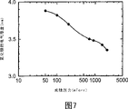
图7是氮化硅膜厚对处理室气体压力的依赖特性图;
图8是形成氮氧化硅膜时的原子态氧和原子态氢的发光强度特性图;
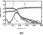
图9是氮氧化硅膜的元素分布特性图;
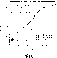
图10是氮氧化硅膜的电流电压特性图;
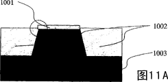
图11A~图11C是浅沟隔离层的剖面原理图;
图12是在凹凸的硅表面上形成的立体晶体管的剖面结构图;
图13是闪存元件的剖面结构示意图;
图14是分阶段说明本发明的闪存元件的形成方法的示意性剖面结构图;
图15是分阶段说明本发明的闪存元件的形成方法的示意性剖面结构图;
图16是分阶段说明本发明的闪存元件的形成方法的示意性剖面结构图;
图17是分阶段说明本发明的闪存元件的形成方法的示意性剖面结构图;
图18是制作在金属衬底SOI上的MOS晶体管的剖面结构示意图;
图19是适应于玻璃衬底和塑料衬底等的等离子体装置示意图;
图20是绝缘膜状的多晶硅晶体管的剖面结构示意图;
图21是三维LSI的剖面结构原理图。
本发明的最佳实施方式
以下,参照附图详细说明采用本发明的优选实施方式。
(第一实施方式)
首先,说明使用等离子体在低温下进行的氧化膜的形成。
图1是使用径向线缝隙天线的等离子体装置的剖面图;
图1是用于本发明的、使用径向线缝隙天线的等离子体处理装置的一个例子的剖面图。
在本实施方式中,为了除去对硅表面悬挂键进行封端氢,在后面的氧化膜形成工序中使用Kr作为等离子体激励气体,并在同一处理室内连续进行除去表面封端氢的处理和氧化处理。
首先,将真空容器(处理室)101内部抽成真空,接着从喷射板102先导入Ar气体,然后将其切换为Kr气体。而且,将所述处理室101内的压力设定为133Pa(1Torr)左右。
接着,将硅衬底103放置在具有加热机构的试料台104上,并将试料温度设定为400℃左右。如果所述硅衬底103的温度在200-550℃的范围内,则与下述结果大致相同。在前一个的前处理工序中,对所述硅衬底103进行稀氢氟酸清洗,其结果,表面的硅悬挂键被氢封端。
接着,从同轴波导管105向径向线缝隙天线106供给频率为2.45GHz的微波,将所述微波从所述径向线缝隙天线106通过设置于处理室101的部分壁面上的电介质板107,导入到所述处理室101内。导入的微波激励从所述喷射板102导入到所述处理室101内的Kr气体,其结果,在所述喷射板102的正下方形成高密度的Kr等离子体。如果供给的微波的频率在900MHz以上、约10GHz以下的范围,则与下述结果大致相同。
在图1的结构中,喷射板102和衬底103的间隔在本实施方式中设定为6cm。该间隔越窄,就越能进行高速的成膜。在本实施方式中,表示了使用径向线缝隙天线的等离子体装置进行成膜的例子,但也可以使用其他方法将微波导入到处理室内并进行等离子体激励。
通过将所述硅衬底103暴露在用Kr气体激励的等离子体中,使所述硅衬底103的表面受低能量Kr离子的照射,除去其表面封端氢。
图2是利用红外光谱仪对所述硅衬底103表面的硅-氢结合进行分析的结果,表示利用Kr等离子体除去硅表面封端氢的效果,其中,所述Kr等离子体被在133Pa(1Torr)压力下,以1.2W/cm2的功率导入到所述处理室101中的微波激励。
参照图2可知,仅在1秒左右的Kr等离子体照射后,硅-氢结合的特征波数2100cm-1附近的光吸收几乎消失,并在约30秒的照射后,几乎完全消失。即可知,通过约30秒的Kr等离子体照射,可以除去封端硅表面的氢。在本实施方式中,进行1分钟的Kr等离子体照射,除去表面封端氢。
接着,从所述喷射板102导入分压比为97/3的Kr/O2混合气体。此时,维持处理室内的压力在133Pa(1Torr)左右。在混合Kr气体和O2气体的高密度激励等离子体中,处于中间激励状态的Kr*和O2分子碰撞,从而能够高效率地产生大量的原子态氧O*。
在本实施例中,用该原子态氧O*对所述硅衬底103的表面进行氧化。现有的硅表面的热氧化方法,使用O2分子或H2O分子进行氧化,需要800℃以上的非常高的处理温度,而本发明的使用原子态氧的氧化处理,可在400℃左右的非常低的温度下进行氧化。为了增大Kr*和O2的碰撞机会,虽然希望处理室的压力高,但是如果过高,产生的O*之间会发生碰撞,从而返回为O2分子。当然,存在最佳气体压力。
图3表示将处理室内的Kr/O2的压力比保持在97/3的基础上改变所述处理室101内的气体压力时,所形成的氧化膜厚度与处理室内压力之间的关系。其中,在图3中,将硅衬底103的温度设定为400℃,进行10分钟的氧化处理。
参照图3可知,在所述处理室101内的压力为约133Pa(1Torr)时,氧化速度最快,该压力及其附近的压力条件是最佳的。该最佳压力不限于所述硅衬底103的面方位为(100)面的情况,也适用于任何面方位的硅表面。
形成期望膜厚的氧化硅膜后,停止导入微波能,并结束等离子体激励,进而将Kr/O2混合气体置换为Ar气体来结束氧化工序。在本工序前后使用Ar气体的原因在于,用比Kr便宜的气体作为净化气体。此外,可回收再利用本工序中使用过的Kr气体。
接以上的氧化膜形成之后,实施电极形成工序、保护膜形成工序、氢烧结处理工序等,来完成包含晶体管和电容的半导体集成电路器件。
在通过升温释放来测定在上述过程形成的氧化硅膜中的氢含量时,在3nm膜厚的氧化硅膜中,按面密度换算时,氢含量为1012/cm2以下。特别是在漏电流小的氧化膜中,按面密度换算时,可知氧化硅膜内的氢含量为1011/cm2以下。另一方面,按面密度换算,在氧化膜形成之前没有进行Kr等离子体暴露的氧化膜含有超过1012/cm2的氢。
此外,用原子力显微镜测定并比较剥离在上述过程形成的氧化硅膜后的硅表面和氧化膜形成前的硅表面的粗糙度时,得知硅表面的粗糙度没有变化。即,即使在除去封端氢并进行氧化后,硅表面也不粗糙。
图4是用全反射X射线荧光光谱仪分析的、根据上述过程形成的氧化硅膜中的Kr密度在深度方向的分布图。其中,图4是关于硅(100)面的结果,但这不局限于(100)面,即使是其他方位,也可以获得同样的结果。
在图4的实验中,将Kr中的氧的分压设定为3%,将处理室内的压力设定为133Pa(1Torr),并在衬底温度为400℃时进行等离子体氧化处理。
参照图4,氧化硅膜中的Kr密度随着远离衬底的硅表面而增大,并在氧化硅膜表面,其密度达到2×10¹¹/cm2左右。因此可知,根据上述过程获得的氧化硅膜是这样的膜:在距离衬底的硅表面4nm以上的区域,膜中的Kr浓度一定,在距离硅表面4nm以下的区域,Kr浓度朝硅/氧化硅膜的界面的方向减少。
图5表示在根据上述过程获得的氧化硅膜中,漏电流对施加电场的依赖性。其中,图5的结果表示氧化硅膜的膜厚为4.4nm时的特性。作为比较,在图5中示出了在氧化膜形成前没有进行Kr等离子体暴露的、同一厚度的氧化膜的漏电流特性。
参照图5可知,没有在Kr等离子体中暴露过的氧化硅膜的漏电流特性与现有的热氧化膜的漏电流特性相同,因此,即使根据Kr/O2微波进行氧化处理,也不能明显改善所得氧化膜的漏电流特性。相反,根据本实施方式的方法,通过照射Kr等离子体来除去封端氢后,导入Kr/O2气体进行氧化后所形成的氧化硅膜,与通过现有的微波等离子体形成的氧化硅膜相比,在同一电场中的漏电流减少了2~3个数量级,显示出非常好的低漏电流特性。并得知即使是膜厚薄至1.7nm的氧化硅膜,也同样能够改善漏电流特性。
图6表示改变所述氧化硅膜的膜厚,来测定本实施方式的氧化硅膜的漏电流特性的结果。其中,在图6中,△表示现有的热氧化膜的漏电流特性,○表示省略在Kr等离子体中进行暴露,用Kr/O2等离子体进行氧化时的氧化硅膜的漏电流特性,而●表示在所述Kr等离子体中进行暴露后,并用所述Kr/O2等离子体进行氧化的本实施例方式的氧化硅膜的漏电流特性。此外,在图6中,用■表示的数据表示在后面说明的氮氧化膜的漏电流特性。
参照图6可知,○所示的省略了在Kr等离子体中进行的暴露工序并通过等离子体氧化工序形成的氧化硅膜的漏电流特性与△所示的热氧化膜的漏电流特性一致,而●所示的本实施方式的氧化硅膜的漏电流特性比○所示的漏电流特性降低了2~3个数量级。此外还可知,本实施方式的氧化硅膜,即使膜厚约为1.5nm,也比得上厚度为2nm的热氧化膜,可以实现1×10⁻²A/cm2的漏电流。
此外,对于由本实施方式获得的氧化硅膜,测定硅/氧化硅膜界面能级密度对面方位的依赖性时,发现在任何面方位的硅表面中,都能够获得约1×1010cm-2eV-1的非常低的界面能级密度。
另外,对于耐压性、热载流子抗性、使应力电流流过时的直至氧化硅膜被破坏的电荷量QBD(Charge-to-Breakdown)等的电特性、可靠性,由本实施方式形成的氧化膜显示出与现有的热氧化膜相同或其之上的良好特性。
如上所述,除去表面封端氢后,通过用Kr/O2高密度等离子体进行硅氧化工序,即使在400℃的低温中,也可以在所有面方位的硅上形成优良的氧化硅膜。获得这种效果的原因在于,通过除去封端氢,氧化膜中的氢含量减少,并且在氧化膜中含有Kr。因氧化膜中的氢很少,氧化硅膜内的元素的弱结合减少,而且通过含有Kr,缓和了膜中和Si/SiO2界面中的应力,使膜中电荷和界面能级密度降低,从而大幅度地改善了氧化硅膜的电特性。
特别是以面密度换算,氢浓度在1012/cm2以下,最好在1011/cm2以下,并含有5×1011/cm2以下的Kr时,将有助于氧化硅膜的电特性、可靠性的改善。
为了实现本发明的氧化膜,除了图1的装置以外,也可以使用能够用等离子体在低温下进行氧化膜形成的其他等离子体处理装置。例如,可以用两级喷射板型等离子体处理装置,该装置具有排出用于通过微波来激励等离子体的Kr气体的第一气体排出结构、以及排出氧气的与所述第一气体排出结构不同的第二气体排出结构。
再有,在本实施方式中,在形成期望膜厚的氧化硅膜时停止导入微波并结束等离子体激励,而且将Kr/O2混合气体置换为Ar气体并结束氧化工序,但也可以这样结束处理,即,在停止导入所述微波能之前,将压力继续保持在133Pa(1Torr)左右的情况下,从喷射板102导入分压比为98/2的Kr/NH3混合气体,在氧化硅膜上形成约0.7nm的氮化硅膜后。根据该方法,可获得在表面上形成了氮化硅膜的氮氧化硅膜,从而可以形成具有更大介电常数的绝缘膜。
(第二实施方式)
下面,论述使用等离子体在低温下进行的氮化膜形成。在氮化膜形成中使用与图1相同的装置。
在本实施方式中,为了形成良好的氮化膜,除去封端氢和形成氮化膜时最好使用Ar或Kr作为等离子体激励气体。
以下表示使用Ar时的一例。
首先,对真空容器(处理室)101进行排气,使其内成为真空,接着从喷射板102导入Ar气体并将处理室内的压力设定在13.3Pa(100mTorr)左右。
接着,将在其之前的前工序中通过加氢水清洗、从而其表面的硅悬挂键被氢封端的硅衬底103导入到所述处理室101中,并装载在具有加热机构的试料台104上。而且将试料的温度设定为500℃。如果该温度在330-550℃的范围内,则下述结果几乎不变。
接着,从同轴波导管105通过径向线缝隙天线106及电介质板107,向处理室内供给2.45GHz的微波,在处理室内产生高密度的Ar等离子体。如果供给的微波频率在900MHz以上、10GHz以下的范围,则以下所述的结果几乎不变。喷射板102和衬底103的间隔在本实施方式中设定为6cm。该间隔越窄,就越能进行高速的成膜。还有,在本实施方式中,表示了通过使用径向线缝隙天线的等离子体装置来进行成膜的例子,但也可以使用其他方法将微波导入到处理室内。
这样,暴露于由Ar气体激励的等离子体中的硅表面受到低能量的Ar离子照射,从而其表面封端氢被除去。本实施方式,在Ar等离子体中暴露1分钟。
接着,在Ar气体中以分压比为2%混合NH3气体并从喷射板102导入。此时,处理室内的压力保持在13.3Pa(100mTorr)左右。在混合Ar气体和NH3气体的高密度激励等离子体中,处于中间激励状态的Ar*和NH3分子碰撞,从而高效率地产生NH*原子团。该NH*原子团对硅衬底表面进行氮化。
接着,在形成期望膜厚的氮化硅膜时停止导入微波能,并结束等离子体激励,而且将Ar/NH3混合气体置换为Ar气体,并结束氮化工序。
在以上的氮化膜形成后,进行电极形成工序、保护膜形成工序、氢烧结处理工序等,从而完成包含晶体管和电容的半导体集成电路器件。
在本实施方式中,示出了通过使用径向线缝隙天线的等离子体装置来形成氮化膜的例子,但也可以使用其他方法将微波导入处理室内。此外,在本实施方式中,在等离子体激励气体上使用Ar,但使用Kr也可以获得同样的结果。此外,在本实施方式中,在等离子体处理气体上使用NH3,但也可以使用N2和H2等的混合气体。
在本发明的氮化硅膜形成中,在除去表面封端氢后,在等离子体中含有氢仍是一个重要的条件。因为等离子体中具有氢,所以在氮化硅膜内及界面的悬挂键上形成Si-H、N-H结合从而被封端,其结果,失去氮化硅膜和截面的电子捕获。
本发明的氮化膜中具有Si-H结合、N-H结合的情况是分别通过测定红外吸收光谱、X射线光电子光谱确认的。因为氢的存在,所以CV特性的磁滞消失,硅/氮化硅膜界面能级密度也被很低地抑制到2×1010cm-2。使用稀有气体(Ar或Kr)和N2/H2的混合气体来形成氮化硅膜时,通过使氢气体的分压为0.5%以上,可以显著地减少膜中的电子和空穴的捕获。
图7表示以上述过程制作的氮化硅膜厚对压力的依赖性。其中,在图7的实验中,将Ar/NH3的分压比设定为98/2,成膜时间为30分钟。
参照图7可知,降低处理室的压力,增加稀有气体(Ar或Kr)对NH3(或N2/H2)施加的能量时,会加快氮化膜的成长速度。从氮化膜形成效率的观点来看,气体压力在6.65~13.3Pa(50~100mTorr)的范围时较好,但是如在其他实施方式中所述的那样,在连续进行氧化和氮化的工序中,可统一在适合的压力上、例如133Pa(1Torr)进行氮化,从生产率的观点来看这也是较好的条件。此外,稀有气体中的NH3(或N2/H2)的分压在1~10%的范围时较好,在2~6%时更好。
由本实施方式获得的氮化硅膜的介电常数为7.9,该值大约相当于氧化硅膜的介电常数的两倍。
在测定由本实施方式获得的氮化硅膜的电流电压特性时发现:在膜厚为3.0nm(按介电常数换算相当于氧化膜为1.5nm)的氮化硅膜施加1V电压时,能够获得比膜厚1.5nm的热氧化膜低5-6数量级以上的漏电流特性。这意味着通过使用本实施例的氮化硅膜,可以突破在栅极绝缘膜上使用氧化硅膜的晶体管中成为问题的微细化界限。
上述氮化膜的成膜条件、物理特性(物性的)及电特性并不局限于(100)面方位的硅表面上,而在包含(111)面的所有面方位的硅中同样成立。
由本实施方式获得的较好的结果,不仅在于除去了封端氢,而且还与氮化膜中包含Ar或Kr的情况也有关系。即,在本实施方式的氮化膜中,氮化膜中和硅/氮化膜界面中的应力通过氮化膜中含有的Ar或Kr被缓和,其结果,使氮化硅膜中的固定电荷和界面能级密度降低,大幅度地改善了电特性、可靠性特性。
与氧化硅膜的情况一样,可以认为,包含面密度为5×10¹¹/cm2以下的Ar或Kr有助于改善氧化硅膜的电特性、可靠性。
为了实现本发明的氮化膜,除了图1的装置以外,还可以使用能够用等离子体在低温下进行氧化膜形成的其他等离子体处理装置。例如,可以用两级喷射板型等离子体处理装置,该装置具有排出用于通过微波来激励等离子体的Ar或Kr气体的第一气体排出结构、以及排出NH3(或N/H气体)的与所述第一气体排出结构不同的第二气体排出结构。
(实施方式3)
下面,说明在栅极绝缘膜上使用等离子体的低温氧化膜和氮化膜的双层结构的实施方式。
本实施方式中使用的氧化膜和氮化膜的形成装置与图1相同。在本实施方式中,为了形成氧化膜和氮化膜,将Kr用作等离子体激励气体。
首先,对真空容器(处理室)101进行排气,使其内成为真空,从喷射板102向所述处理室101内导入Ar气体。接着,将导入的气体从最初的Ar切换成Kr,将所述处理室101内的压力设定在133Pa(1Torr)左右。
接着,将在其之前的前工序中实施稀氢氟酸清洗、从而其表面的硅悬挂键被氢封端的硅衬底103导入到所述处理室101中,并装载在配有加热机构的试料台104上。而且将试料的温度设定为400℃。
接着,从所述同轴波导管105向径向线缝隙天线106供给1分钟的频率为2.45GHz的微波,将所述微波通过电介质板107导入到处理室101内。这样,将所述硅衬底103暴露于在所述处理室101内产生的高密度的Kr等离子体中,从而除去其表面封端氢。
接着,将所述处理室101内的压力保持在133Pa(1Torr)左右的情况下,从所述喷射板102导入分压比为98/3的Kr/O2混合气体,在所述硅衬底103的表面上形成1.5nm的氧化硅膜。
接着,暂时停止供给微波,停止导入O2气体。并用Kr对真空容器(处理室)101内进行清洁后,从喷射板102导入分压比为98/2的Kr/NH3混合气体,而且将处理室内的压力设定在133Pa(1Torr)左右的情况下,再次供给频率为2.56GHz的微波,在所述处理室101内产生高密度的等离子体,从而在所述氧化硅膜的表面上形成1nm的氮化硅膜。
接着,在形成期望膜厚的氮化硅膜时,停止导入微波并结束等离子体激励,进而将Kr/NH3混合气体置换成Ar气体,结束氮氧化工序。
在以上氮氧化硅膜形成后,通过实施电极形成工序、保护膜形成工序、氢烧结处理工序,来完成包含晶体管和电容的半导体集成电路器件。
在测定这样形成的层叠栅极绝缘膜的有效介电常数时,获得约为6的值。另外,漏电流特性、耐压特性、热载流子抗性等电性能、可靠性特性也与前面实施方式1的情况一样良好。此外,在获得的栅极绝缘膜中没有发现对硅衬底103的面方位的依赖性,因此在(100)面以外的任何面方位的硅上都可以形成良好特性的栅极绝缘膜。这样,可以实现同时具备氧化膜的低界面能级特性和氮化膜的高介电常数特性的栅极绝缘膜。
在本实施方式中,示出了在硅的一侧形成氧化膜的氧化膜、氮化膜的双层结构,但根据目的,可以转换氧化膜、氮化膜的顺序,并且还可以形成氧化膜/氮化膜/氧化膜、氮化膜/氧化膜/氮化膜等多种层叠膜。
(第四实施方式)
下面,说明在栅极绝缘膜上使用等离子体的低温氮氧化膜的实施方式。
在本实施方式中使用的氮氧化膜形成装置与图1相同。在本实施方式中,将Kr用作等离子体激励气体。
首先,对真空容器(处理室)101进行排气,使其内成为真空,从喷射板102向所述处理室101内导入Ar气体。接着,将导入到所述处理室101中的气体从Ar切换成Kr,并将处理室内的压力设定在133Pa(1Torr)左右。
接着,将在其之前的前工序中实施稀氢氟酸清洗、从而其表面的硅悬挂键被氢封端的硅衬底103导入到所述处理室101中,并装载在配有加热机构的试料台104上。而且将试料的温度设定为400℃。
接着,从所述同轴波导管105向径向线缝隙天线106供给1分钟的频率为2.45GHz的微波,将所述微波从径向线缝隙天线106通过电介质板107导入到处理室101内,在所述处理室101内产生高密度的Kr等离子体。这样,通过将所述硅衬底103的表面暴露在由Kr气体激励的等离子体中,来除去其表面封端氢。
接着,将所述处理室101的压力维持在133Pa(1Torr)左右,从所述喷射板102导入分压比为96.5/3/0.5的Kr/O2/NH3混合气体,在硅表面上形成3.5nm的氮氧化硅膜。在形成期望膜厚的氮氧化硅膜时,停止导入微波能,结束等离子体激励,并将Kr/O2/NH3混合气体置换为Ar气体,结束氮氧化工序。
在以上的氧化膜形成后,实施电极形成工序、保护膜形成工序、氢烧结处理工序等,来完成包含晶体管和电容的半导体集成电路器件。
如图8所示,通过发光分析测定的原子态氧O*的发生密度在Kr/O2/NH3气体的混合比为97/3/0~95/3/2的范围内没有实质性变化,但如果增大NH3的比率超出此范围时,则原子态氧的发生量将会减少,而代之,原子态氢的量会增加。尤其,Kr/O2/NH3气体的混合比为96.5/3/0.5时,漏电流减少到最小,绝缘耐压、电荷注入也提高。
图9表示用二次离子质谱仪测定的、本实施方式的氮氧化膜内的硅、氧、氮的浓度分布。其中,在图9中,横轴表示从氮氧化膜的表面开始的深度。在图9中,可看到硅、氧、氮的分布在膜内平缓地变化,这并不是因为氮氧化膜的膜厚不均匀,而是因为蚀刻的均匀性差。
参照图9可知,所述氮氧化膜中的氮的浓度在硅/氮氧化硅膜界面和氮氧化硅膜表面中较高,在氮氧化膜中央部分减少。该氮氧化膜所取入的氮含量与硅和氧相比为几成以下。
图10表示本实施方式的氮氧化膜的漏电流对施加电场的依赖性。其中,在图10中,作为比较,还表示了在通过微波等离子体的氧化膜形成之前没有进行Kr等离子体的暴露处理的、同一膜厚的氧化膜的漏电流特性和通过热氧化形成的氧化膜的漏电流特性。
参照图10可知,在通过Kr等离子体照射除去封端氢后,导入Kr/O2/NH3气体进行氮氧化的本实施方式的氮氧化膜中,与根据现有方法形成的氧化膜相比,同一电场下的漏电流的值减小了2~4个数量级,从而能够获得良好的低漏电流特性。
此外,在前面说明的图6中,用■表示这样形成的氮氧化膜的漏电流特性和膜厚的关系。
再次参照图6可知,根据本实施方式,进行Kr照射后形成的氮氧化膜具有与根据相同工序形成的氧化膜相同的漏电流特性,特别是在膜厚为约1.6nm时,漏电流的值也不过为1×10⁻²A/cm2。
另外,在本实施方式的氮氧化膜中,耐压特性、热载流子抗性等电特性、可靠性也优于前面实施方式1的氧化膜。此外,也没有发现对硅衬底的面方位的依赖,因此,不仅在硅的(100)面,而且在任何面方位的硅表面上都能够形成优良特性的栅极绝缘膜。
如上述那样,除去表面封端氢后,通过用Kr/O2/NH3的高密度等离子体进行硅氮氧化工序,即使在400℃的低温中,也可以在所有面方位的硅表面上形成具有优良的特性和膜质量的氮氧化硅膜。
在本实施方式中能够获得这样良好的效果的原因,不仅在于通过除去封端氢,减少了氮氧化膜中的氢含量,而且还在于在氮氧化膜中含有几成以下的氮。在本实施方式的氮氧化膜中,Kr的含量与实施方式1的氧化膜相比大约在1/10以下,而取代Kr含有更多的氮。即,在本实施方式中,由于氮氧化硅膜中的氢少,所以氮氧化膜中的弱结合的比例减少,而通过含有氮,缓和了膜中和Si/SiO2界面中的应力,其结果,使膜中电荷和界面能级的密度降低,从而大幅度地改善了所述氮氧化膜的电特性。特别是所述氮氧化膜中的氢浓度以面密度换算时在1012cm-2以下,最好减少到1011cm-2以下的情况,以及膜中含有浓度为硅或氧浓度的几成以下的氮的情况,被认为有助于氮氧化硅膜的电特性、可靠性的改善。
此外,在本实施方式中,在形成期望膜厚的氮氧化膜时停止导入微波能,并结束等离子体激励,而且将Kr/O2/NH3混合气体置换为Ar气体并结束氮氧化工序,但也可以在停止导入该微波能之前,将压力保持在133Pa(1Torr)左右的情况下,从所述喷射板102导入分压比为98/2的Kr/NH3混合气体,在氮氧化膜的表面上形成约0.7nm的氮化膜后结束氮氧化工序。根据该方法,可在氮氧化硅膜的表面上形成氮化硅膜,从而可形成介电常数更大的绝缘膜。
(第5实施方式)
下面,示出根据本发明第5实施方式的半导体器件的形成方法,该方法在构成浅沟隔离层的元件分离侧壁部分的角部分或在具有凹凸的表面形状的硅表面上形成高质量的氧化膜。
图11A是浅沟隔离层的原理图。
参照图11,图示的浅沟隔离层是这样形成的:即,在硅衬底1003表面上通过等离子体蚀刻来形成隔离沟槽,将形成的沟槽用通过CVD(化学气相沉积)法形成的氧化硅膜1002填充,并且例如用CMP(化学机械抛光)法等对所述氧化硅膜1002进行平坦化。
在本实施方式中,在根据CMP法的所述氧化硅膜1002的研磨工序后,通过将硅衬底暴露于800-900℃的氧化性气氛中来进行牺牲氧化(Sacrificial oxidation),将通过牺牲氧化形成的氧化硅膜在含有氢氟酸的药液中进行蚀刻,获得氢封端的硅表面。在本实施方式中按与实施方式1同样的过程,通过Kr等离子体除去表面封端氢,然后导入Kr/O2气体,形成约2.5nm的氧化硅膜。
根据本实施方式,如图11所示,在浅沟隔离层的角部分中,氧化硅膜以均匀的厚度形成,不发生氧化硅膜的膜厚变薄。包含利用该Kr等离子体的等离子体氧化法形成的浅沟隔离层部分的氧化硅膜整体的QBD(Charge to Breakdown)特性非常良好,即使在注入电荷量为102C/cm2时,也不会引起漏电流的上升,从而能够大幅度地改善器件的可靠性。
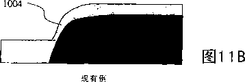
如图11B所示,在通过现有的热氧化法来形成所述氧化硅膜时,随着浅沟隔离层的锥形角增大,浅沟隔离层角部分中的膜很大程度地变薄,但根据本发明的等离子体氧化,即使锥形角增大,也不会使浅沟隔离层角部分的氧化硅膜变薄。因此,本实施例,在浅沟隔离层结构中,通过使沟槽的锥形角接近90度,可以减少元件分离区域的面积。从而能够进一步提高半导体元件的集成度。在现有的热氧化技术中,因图11B所示的沟槽角部分中的热氧化膜的薄膜化的约束,在元件分离部分中使用约70度左右的锥形角,而根据本发明,可使用90度的角度。
图12是根据实施方式1的过程在硅衬底上形成3nm厚度的氧化硅膜的剖面,其中,所述硅衬底具有将硅衬底蚀刻到约90度的凹凸表面形状。
参照图12,可知在任何面上都形成了均匀膜厚的氧化硅膜。
在这样形成的氧化膜中,漏电流和耐压等电特性良好,因此,根据本发明,能够实现具有纵向结构等多个面方位的硅立体结构的、高密度的半导体集成器件。
(第6实施方式)
下面,说明本发明第6实施方式的闪存元件,其中,使用了上述在低温下使用等离子体的氧化膜及氮化膜,或氮氧化膜的形成技术。此外,虽然在以下的说明中,作为一个例子公开了闪存元件,但本发明也适用于有同样层叠结构的EPROM、EEPROM等。
图13是本实施方式的闪存元件的剖面结构示意图。
参照图13,所述闪存元件形成在硅衬底1201上,由形成在所述硅衬底1201上的隧道氧化膜1202、作为形成在所述硅衬底1201上的浮置栅极的第一多晶硅栅极1203、依次形成在所述多晶硅栅极1203上的氧化硅膜1204和氮化硅膜1205、形成在所述氮化硅膜1205上构成控制栅极的第二多晶硅栅极1206构成。在图13中,省略了源极区、漏极区、接触孔、布线图形等的图示。所述氧化硅膜1202根据第一实施方式中说明的氧化硅膜形成方法来形成,而氧化硅膜1204和氮化膜1205的层叠结构根据实施方式3中说明的氮化硅膜形成方法来形成。
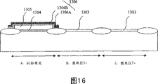
图14~图17是分段说明本实施方式的闪存元件的制造方法的示意性剖面图。
参照图14,在硅衬底1301上通过场氧化膜1302来划分闪存存储单元区域A、高电压晶体管区域B以及低电压晶体管区域C,在各所述区域A~C中,在所述硅衬底1301的表面上形成氧化硅膜1303。所述场氧化膜1302可以通过硅局部氧化法(LOCOS法)或浅沟隔离法等形成。
在本实施方式中,将Kr用作等离子体激励气体来除去表面封端氢,并形成氧化膜及氮化膜。氧化膜、氮化膜形成装置与图1相同。
接着,在图15的工序中,从存储单元区域A中除去所述氧化硅膜1303,通过稀氢氟酸清洗对硅表面进行氢封端。而且,与前面的实施方式1一样,形成隧道氧化膜1304。
即,与前面的实施方式1一样,对所述真空容器(处理室)101进行排气,使其内成为真空,并从喷射板102向所述处理室101中导入Ar气体。接着,将所述Ar气体切换为Kr气体,将处理室101中的压力设定为1Torr左右。
接着,将除去所述氧化硅膜1303的、对硅表面进行稀氢氟酸处理的所述硅衬底1301作为图1的硅衬底103导入到所述处理室101内,并装载在具有加热机构的试料台104上。而且,将试料台的温度设定为400℃。
而且,从所述同轴波导管105向径向线缝隙天线106供给1分钟的频率为2.45GHz的微波,将所述微波从径向线缝隙天线106通过所述电介质板107导入到所述处理室101内。将所述硅衬底1301的表面暴露在如述形成于所述处理室101中的高密度Kr等离子体中,从而,从所述硅衬底1301的硅表面除去封端氢。
接着,从所述喷射板102导入Kr气体、O2气体,在所述区域A以3.5nm的厚度形成作为所述隧道绝缘膜的氧化硅膜1304,接着堆积第一多晶硅层1305,以覆盖所述氧化硅膜1304。
接着,在高电压和低电压晶体管形成区域B、C中,通过所述第一多晶硅层1305构图而将其除去,仅在存储单元区域A的隧道氧化膜1304上,保留第一多晶硅图形1305。
在所述蚀刻后进行清洗,对多晶硅图形1305的表面进行氢封端。
接着,在图16的工序中,与前面第三实施方式一样,形成具有下部氧化膜1306A和上部氮化膜1306B的ON结构的绝缘膜1306,以覆盖所述多晶硅图形1305。
该ON膜如下形成。
对真空容器(处理室)101进行排气,使其内成为真空,将从喷射板102导入的Ar气体切换为Kr气体并进行导入,将处理室内的压力设定为133Pa(1Torr)左右。接着,将进行所述氢封端的、具有多晶硅图形1305的硅衬底1301导入到所述处理室101内,并装载在具有加热机构的试料台104上。而且,将试料台的温度设定为400℃。
接着,从所述同轴波导管105向径向线缝隙天线106供给大约1分钟的频率为2.45GHz的微波,将所述微波从径向线缝隙天线106通过所述电介质板107导入到所述处理室101内,产生高密度的Kr等离子体。其结果,所述多晶硅图形1305的表面被暴露在Kr气体中,使表面封端氢被除去。
接着,将所述处理室101内的压力维持在133Pa(1Torr)左右的情况下,从所述喷射板102向所述处理室101内导入Kr/O2混合气体,在多晶硅表面上形成3nm的氧化硅膜。
接着,在暂时停止微波的供给后,停止Kr气体、O2气体的导入,并对真空容器(处理室)101内进行排气后,从喷射板102导入Kr气体和NH3气体。将所述处理室101内的压力设定为13.3Pa(100mTorr)左右,再次将2.45GHz的微波从所述径向线缝隙天线106供给到所述处理室101内,在处理室内产生高密度的等离子体,在氧化硅膜表面上形成6nm的氮化硅膜。
这样形成9nm的ON膜时,获得的ON膜的膜厚是一样的,而且没有观察到对多晶硅面方位的依赖性,从而得知可获得非常均匀的膜。
在这样形成所述ON膜后,在图17的工序中,通过构图从高电压及低电压晶体管区域B、C中除去绝缘膜1306,接着在高电压及低电压晶体管区域B、C上进行用于阈值电压控制的离子注入。并且,除去形成在所述区域B、C上的氧化膜1303,在所述区域B上形成5nm厚度的栅极绝缘膜1307,然后在所述区域C上形成3nm厚度的栅极绝缘膜1308。
然后,在包含场氧化膜1302的整体结构上依次形成第二多晶硅层1309和硅化物层1310,进而对所述第二多晶硅层1309和硅化物层1310进行构图,在所述高电压晶体管区域B和低电压晶体管区域C中分别形成栅极1311B和1311C。此外,对应于所述存储器区域A,形成栅极1311A。
在图17的工序后,根据标准的半导体工序,形成源极区和漏极区,之后形成层间绝缘膜和接触孔及布线图形等而完成元件。
在本发明中,这些绝缘膜1306A、1306B,即使将其膜厚减少到现有的氧化膜和氮化膜的约一半,也可以维持良好的电特性。即,这些氧化硅膜1306A和氮化硅膜1306B,即使对它们进行薄膜化,也能具有良好的电特性,并且致密、质量高。此外,在本发明中,所述氧化硅膜1306A和氮化硅膜1306B在低温下形成,因此在栅极多晶硅和氧化膜的界面上不产生热存积等,可获得良好的界面。
本发明的闪存元件在低电压下进行信息的写入和删除动作,从而可以抑制衬底电流的产生,进而能够抑制隧道绝缘膜的恶化。因此,可以高成品率地制造二维排列本发明的闪存元件而形成的非易失性半导体存储装置,并且使该半导体存储装置显示出稳定的特性。
本发明的闪存元件,对应于所述绝缘膜1306A、1306B具有良好的膜质量,其漏电流较小,而且可以减小膜厚而不增加漏电流,因此可在5V左右的工作电压下进行写入或删除动作。其结果,闪存元件的存储保持时间比以往增大了两个数量级以上,可重写的次数也增大了两个数量级以上。
此外,绝缘膜1306的膜结构不限于上述ON结构,也可以是同于实施方式1的由氧化膜构成的O结构、同于实施方式2的由氮化膜构成的N结构、或是同于实施方式4的氮氧化膜。此外,所述绝缘膜1306也可以是由氮化膜及氧化膜构成的NO结构、依次层叠氧化膜、氮化膜及氧化膜的ONO结构、以及层叠氮化膜、氧化膜、氮化膜、氧化膜的NONO结构等。选择一种结构作为所述绝缘膜1306时,可以考虑周边电路的高电压晶体管和低电压晶体管的栅极绝缘膜间的匹配性和共用可能性等,根据目的进行选择。
(第7实施方式)
使用图1的装置,可将利用Kr/O2微波激励高密度等离子体的栅极绝缘膜的形成、或将利用Ar(或Kr)/NH3(或N2/H2)微波激励高密度等离子体的栅极氮化膜的形成,应用于不能使用现有的高温工序的、金属层存在于衬底硅内的硅-绝缘体(金属衬底SOI)晶片上的半导体集成电路器件的形成上。特别是在硅的膜厚薄的、完全耗尽的SOI结构中,根据本发明的除去封端氢的效果比较明显。
图18是具有金属衬底SOI结构的MOS晶体管的剖面图。
参照图18,1701是n+型或p+型的低电阻半导体层,1702是NiSi等硅化物层,1703是TaN、TiN等导电性氮化物层;1704是Cu等金属层,1705是TaN、TiN等导电性氮化物层,1706是n+型或p+型的低电阻半导体层,1707是AlN、Si3N4等氮化物绝缘膜,1708是SiO2膜,1709是SiO2层、BPSG层或将它们组合起来的绝缘膜层,1710是n+型漏极区,1711是n+型源极区,1712是p+型漏极区,1713是p+型源极区,1714、1715是以<111>方向取向的硅半导体层,1716是根据本发明实施方式1的过程、通过Kr照射除去表面封端氢后、利用Kr/O2微波激励高密度等离子体形成的SiO2膜,1717和1718分别是用Ta、Ti、TaN/Ta、TiN/Ti等形成的nMOS晶体管和pMOS晶体管的栅极,1719是nMOS晶体管的源极,1720是nMOS晶体管和pMOS晶体管的漏极。1721是pMOS晶体管的源极。1722是衬底表面电极。
在这种用TaN或TiN保护的含有Cu层的衬底中,为了抑制Cu的扩散,热处理温度必须在约700℃以下。n+型或p+型的源极区或漏极区在As+、AsF2 +或BF2 +的离子注入后,在550℃的热处理中形成。
在具有图18的器件结构的半导体器件中,对在栅极绝缘膜上使用热氧化膜的晶体管的亚阈值(sub-threshold)特性和在Kr等离子体照射中除去表面封端氢后、通过Kr/O2微波激励高密度等离子体处理形成栅极绝缘膜的晶体管的亚阈值特性进行比较时,在通过热氧化形成的栅极绝缘膜情况下的亚阈值特性上可观察到弯折或泄漏,而根据本发明形成的栅极绝缘膜情况下的亚阈值特性却非常好。
此外,如果具有台面形元件分离结构,则在台面元件分离结构的侧壁部分会呈现出与硅平面部分不同面方位的硅表面,但是可以通过使用Kr的等离子体氧化来形成栅极绝缘膜,从而对台面元件分离的侧壁部分进行大致与平面部分相同的均匀的氧化,进而可以获得良好的电特性、高可靠性。
此外,根据第二实施方式的过程,即使将用Ar/NH3形成的氮化硅膜用作栅极绝缘膜,也能够制造出具有非常良好的电特性、高可靠性的金属衬底SOI集成电路器件。
在本实施方式中,即使是氮化硅膜的厚度为3nm(以介电常数换算时相当于1.5nm的氧化硅膜膜厚),也可以获得良好的电特性,并且与使用3nm的氧化硅膜相比,可以将晶体管的驱动能力提高2倍左右。
(第8实施方式)
图19是本发明第8实施方式的制造装置一例的原理图,该装置用于对形成液晶显示元件和有机场致发光元件等的玻璃衬底或塑料衬底等大型长方形衬底上所形成的多晶硅或非晶硅层进行氧化处理、氮化处理、或氮氧化处理。
参照图19,通过使真空容器(处理室)1807内处于减压状态,接着从设置于所述处理室1807内的喷射板1801导入Kr/O2混合气体,进而通过螺纹沟泵1802对所述处理室1807内进行排气,将所述处理室1807内的压力设定为133Pa(1Torr)。然后,将玻璃衬底1803放置在具有加热机构的试料台1804上,并将玻璃衬底的温度设定为300℃。
在所述处理室1807中设置多个矩形波导管1805,接着从所述多个矩形波导管1805的各个缝隙部分通过电介质板1806向所述处理室1807内导入微波,在所述处理室1807内产生高密度的等离子体。此时,设置于所述处理室1807中的喷射管1801具有将从波导管发射的微波作为表面波向左右传播的波导路径的作用。
图20表示使用图19的装置来制造本发明的栅极绝缘膜或栅极氮化膜,并形成用于驱动液晶显示元件、有机EL发光元件等的,或用于处理电路的多晶硅薄膜晶体管(TFT)的例子。
首先,阐述形成并使用氧化硅膜的例子。
参照图20,1901是玻璃衬底,1902是Si3N4膜,1903是以(111)面为主取向的多晶硅nMOS的沟道层,1905、1906分别是多晶硅nMOS的源极区、漏极区,1904是以(111)面为主取向的多晶硅pMOS的沟道层,1907、1908分别是多晶硅pMOS的源极区、漏极区。1910是多晶硅nMOS的栅极,1911是多晶硅pMOS的栅极,1912是SiO2、BSG、BPSG等绝缘膜,1913、1914是多晶硅nMOS的源极(同时为多晶硅p-MOS的漏极),1915是多晶硅p-MOS的源极。
形成于绝缘膜上的多晶硅在对于绝缘膜垂直的方向上朝向(111)面时是稳定的,并且是结晶性致密的高质量的多晶硅。在本实施方式中,1909是使用图19的装置根据与实施方式1相同的过程做成的、厚度为0.2μm的本发明的氧化硅膜层,在朝向(111)面的多晶硅上400℃下以3nm来形成。
根据本实施方式可知,在晶体管间的元件分离区域的尖角部分中氧化膜也没有变薄,因此在多晶硅上形成平坦部分和边缘部分都为均匀膜厚的氧化硅膜。用于形成源极、漏极区的离子注入不经过栅极绝缘膜进行,而且在400℃下通过电激活来形成。其结果,可以在400℃以下的温度实施所有工序,并且能够在玻璃衬底上形成晶体管。该晶体管的迁移率是电子时约为300cm2/Vsec以上,空穴时约为150cm2/Vsec以上,源极、漏极耐压和栅极耐压时为12V以上。在沟道长度为1.5-2.0nm左右的晶体管中,可进行超过100MHz的高速动作。氧化硅膜的泄漏特性、多晶硅/氧化膜的界面能级特性也良好。
通过使用本实施方式的晶体管,液晶显示元件、有机EL发光元件可以具有大画面、低价格、高速动作、高可靠性。
虽然本实施方式是将本发明的栅极绝缘膜或栅极氮化膜用于多晶硅上的实施方式,但同样也可以应用在用于液晶显示元件等的非晶硅薄膜晶体管(TFT)的、特别是交错型的薄膜晶体管(TFT)的栅极绝缘膜或栅极氮化膜上。
(第9实施方式)
下面,说明了具有金属层的SOI元件、多晶硅元件、非晶硅元件的三维层叠LSI的实施方式。
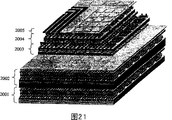
图21是本发明的三维LSI的剖面结构原理图。
在图21中,2001是第一SOI及布线层,2002是第二SOI及布线层,2003是第一多晶硅元件及布线层,2004是第二多晶硅元件及布线层,2005是非晶硅半导体元件和功能材料元件及布线层。
在所述第一SOI及布线层2001和所述第二SOI及布线层2002上,使用在实施方式7中说明的SOI晶体管来制作数字运算处理部分、高精度高速模拟部分、同步DRAM部分、电源部分、接口电路部分等。
在所述第一多晶硅元件和布线层2003中,使用在前面的实施方式6、8中说明的多晶硅晶体管、闪存存储器等来制作并行数字运算部分、功能块间中继部分、存储元件部分等。
另一方面,在所述第二多晶硅元件和布线层2004中,使用所述实施方式8中说明的多晶硅晶体管来形成放大器、AD变换器等并行模拟运算部分。在非晶硅半导体元件、功能材料元件及布线层2005上,制作光传感器、声音传感器、触觉传感器、电波发送接收部分等。
所述非晶硅半导体元件、功能材料元件及设置于布线层2005内的光传感器、声音传感器、触觉传感器、电波发送接收部分的信号由使用所述第二多晶硅元件和设置于布线层2004中的多晶硅晶体管的放大器、AD变换器等并行模拟运算部分处理,而且将该处理在使用所述第一多晶硅元件和布线层2003或所述第二多晶硅元件和设置于布线层2004中的多晶硅晶体管、闪存存储器的并行数字运算部分、存储元件部分中继续进行,进而由使用设置于所述第一SOI和布线层2001或所述第二SOI和布线层2002中的SOI晶体管的数字运算处理部分、高精度高速模拟部分、同步DRAM来处理。
此外,即使设置多个所述第一多晶硅元件和设置于布线层2003中的功能块间中继部分,也不会占很大的芯片面积,并能够调整LSI整体的信号为同步。
根据在上述实施方式中详细说明的本发明的技术可知,能够形成这种三维LSI。
以上,以优选实施例说明了本发明,但本发明并不局限于这些特定的实施例,可在本发明的宗旨内进行各种变形、变更。
工业实用件
根据本发明,在不恶化硅表面的平坦性,不破坏真空的连续工序中,即使在400℃以下的低温下,也可完全除去表面封端氢,因此能够在约500℃以下的低温下、在所有面方位的硅上形成,比用现有的热氧化工序或微波等离子体工序成膜的氧化硅膜特性更优良的、高可靠性的氧化硅膜、氮化硅膜、氮氧化硅膜,从而能够实现高可靠性、高性能的微细晶体管集成电路。
而且,根据本发明,在浅沟隔离层等元件分离侧壁部分的角部分和具有凹凸表面形状的硅表面上,也能够形成漏电流和耐压等特性良好的、薄而高质量的氧化硅膜、氮化硅膜、氮氧化硅膜,从而能够实现将元件分离宽度变小的高密度的元件集成化和具有立体结构的高密度的元件集成化。
此外,通过使用本发明的栅极绝缘膜,可以实现能够大幅增加重写次数的闪存存储元件等。
此外,根据本发明,在形成于绝缘膜上的主要以(111)面取向的多晶硅上,也能够形成高质量的栅极氧化硅膜、栅极氮化硅膜,因此可以实现使用具有高驱动能力的多晶硅晶体管的显示装置,进而可以实现层叠多个晶体管、功能元件的三维集成电路元件,并且此技术所波及的效果很大。
Claims (45)
1.一种半导体器件,包括形成于硅表面上的硅化合物层,其特征在于,
所述硅化合物层至少包含规定的惰性气体,氢含量按面密度换算时在1011/cm2以下。
2.如权利要求1所述的半导体器件,其特征在于,
所述惰性气体至少是氩、氪、氙中的一种。
3.一种半导体器件,是在共用衬底上具有晶体管和电容的半导体存储器件,其中,所述晶体管,具有在硅表面的第一硅化合物层上形成的多晶硅膜,所述电容,包含在多晶硅表面形成的第二硅化合物层,
其特征在于,
所述第一和第二硅化合物层分别至少包含规定的惰性气体,氢含量按面密度换算时在1011/cm2以下。
4.一种半导体器件,将形成于衬底上的多晶硅层或非晶硅层作为活性层,
其特征在于,
在所述硅层的表面上,形成至少包含规定的惰性气体、氢含量按面密度换算时在1011/cm2以下的硅化合物层;
所述半导体器件驱动形成于所述衬底上的显示元件。
5.一种半导体器件的制造方法,用于在硅表面上制造半导体器件,
其特征在于,该方法包括:
将所述硅表面暴露在由第一惰性气体产生的第一等离子体中,除去预先至少存在于部分硅表面的氢的工序;以及
由第二惰性气体和一种或多种气体分子的混合气体产生第二等离子体,并在所述第二等离子体下,在所述硅表面上形成至少包含一部分构成所述气体分子的元素的硅化合物层的工序,所述硅化合物层中的氢含量按面密度换算时在1011/cm2以下。
6.如权利要求5所述的半导体器件的制造方法,其特征在于,
在所述除氢工序之前,包含用含有氢的媒体来处理所述硅表面的工序。
7.如权利要求6所述的半导体器件的制造方法,其特征在于,所述媒体是添加氢的水。
8.如权利要求6所述的半导体器件的制造方法,其特征在于,所述媒体是稀氢氟酸。
9.如权利要求5所述的半导体器件的制造方法,其特征在于,所述硅表面是单晶硅表面。
10.如权利要求9所述的半导体器件的制造方法,其特征在于,所述硅表面由(100)面构成。
11.如权利要求9所述的半导体器件的制造方法,其特征在于,所述硅表面由(111)面构成。
12.如权利要求9所述的半导体器件的制造方法,其特征在于,所述硅表面有多个不同的结晶面。
13.如权利要求12所述的半导体器件的制造方法,其特征在于,所述多个不同的结晶面构成元件分离沟。
14.如权利要求5所述的半导体器件的制造方法,其特征在于,所述硅表面是多晶硅表面。
15.如权利要求5所述的半导体器件的制造方法,其特征在于,所述硅表面是非晶硅表面。
16.如权利要求5所述的半导体器件的制造方法,其特征在于,
所述第一惰性气体和所述第二惰性气体都是从氩气、氪气、氙气构成的组中选择的至少一种气体。
17.如权利要求16所述的半导体器件的制造方法,其特征在于,所述第一惰性气体和所述第二惰性气体相同。
18.如权利要求5所述的半导体器件的制造方法,其特征在于,
所述第二惰性气体由氪气体构成,所述气体分子由氧分子构成,形成氧化硅膜作为所述硅化合物层。
19.如权利要求5所述的半导体器件的制造方法,其特征在于,
所述第二惰性气体是氩气体、或氪气体、或氩和氪的混合气体,所述气体分子由氨分子、或氮分子和氢分子构成,形成氮化硅膜作为所述硅化合物层。
20.如权利要求5所述的半导体器件的制造方法,其特征在于,
所述第二惰性气体是氩气体、或氪气体、或氩和氪的混合气体,所述气体分子由氧分子和氨分子、或氧分子和氮分子及氢分子构成,形成氮氧化硅膜作为所述硅化合物层。
21.如权利要求5所述的半导体器件的制造方法,其特征在于,
所述第一等离子体和所述第二等离子体由微波激励。
22.一种半导体器件的制造方法,用于制造半导体存储器件,所述半导体存储器件在共用衬底上具有晶体管和电容,其中,所述晶体管,具有在硅表面的第一绝缘层上形成的多晶硅膜,所述电容,包含在多晶硅表面形成的第二绝缘层,
其特征在于,该方法包括:
将所述硅表面暴露在由第一惰性气体产生的第一等离子体中,除去预先至少存在于部分所述硅表面上的氢的工序;以及
由第二惰性气体和一种或多种气体分子的混合气体产生第二等离子体,并在所述第二等离子体下,在所述硅表面上形成至少包含一部分构成所述气体分子的元素的硅化合物层来作为所述第一绝缘膜的工序。
23.如权利要求22所述的半导体器件的制造方法,其特征在于,还包括:
将所述多晶硅表面暴露在由第三惰性气体产生的第三等离子体中,来除去预先至少存在于部分所述硅表面的氢的工序;以及
由第四惰性气体和一种或多种气体分子的混合气体产生第四等离子体,在所述第四等离子体下,在所述多晶硅表面上形成至少包含一部分构成所述气体分子的元素的硅化合物层来作为所述第二绝缘膜的工序。
24.如权利要求23所述的半导体器件的制造方法,其特征在于,
所述第一和第三惰性气体至少由从Ar、Kr及Xe构成的组中选择的一种气体构成。
25.如权利要求23所述的半导体器件的制造方法,其特征在于,
所述第二和第四惰性气体由Kr构成,所述第一和第二绝缘膜由氧化硅膜构成。
26.如权利要求23所述的半导体器件的制造方法,其特征在于,
所述第二和第四惰性气体由Ar或Kr构成,所述第一和第二绝缘膜由氮化膜或氮氧化膜构成。
27.如权利要求22至26中任何一项所述的半导体器件的制造方法,其特征在于,
所述第一和第二等离子体由微波激励。
28.一种半导体器件的制造方法,将衬底上的多晶硅层或非晶硅层作为活性层,
其特征在于,该方法包括:
在所述衬底上形成由多晶硅层或非晶硅层构成的硅层的工序;
将所述硅层表面暴露在由第一惰性气体产生的等离子体中,除去至少存在于部分所述硅层表面的氢的工序;以及
由第二惰性气体和一种或多种气体分子的混合气体产生第二等离子体,在所述硅表面上形成至少包含一部分构成所述气体分子的元素的硅化合物层的工序,所述硅化合物层中的氢含量按面密度换算时在1011/cm2以下。
29.如权利要求28所述的半导体器件的制造方法,其特征在于,
所述第一惰性气体至少由从Ar、Kr和Xe构成的组中选择的一种气体构成。
30.如权利要求28所述的半导体器件的制造方法,其特征在于,
所述第二惰性气体由Kr构成,所述硅化合物层由氧化硅膜构成。
31.如权利要求28所述的半导体器件的制造方法,其特征在于,
所述第二惰性气体由Ar或Kr构成,所述硅化合物层由氮化膜或氮氧化膜构成。
32.如权利要求28所述的半导体器件的制造方法,其特征在于,
所述第一及第二等离子体由微波激励。
33.一种半导体器件,其特征在于,包括半导体区和直接形成在该半导体区上的绝缘膜,在所述半导体区和所述绝缘膜之间的界面,表面封端氢按面密度换算时在1011/cm2以下。
34.一种半导体器件,其特征在于,具有将形成于衬底上的多晶硅层或非晶硅层作为活性层而在所述硅层之上直接形成的绝缘膜,在所述硅层和所述绝缘膜之间的界面,表面封端氢按面密度换算时在1011/cm2以下。
35.如权利要求33或34所述的半导体器件,其特征在于,所述绝缘膜包含氧化硅、氮化硅以及氮氧化硅中的至少一种。
36.如权利要求33或34所述的半导体器件,其特征在于,所述绝缘膜包含Ar、Kr和Xe中的至少一种。
37.如权利要求33或34所述的半导体器件,其特征在于,所述绝缘膜包含氮化硅和氮氧化硅中的至少一种,其表面部分的氮浓度大于中央部分的氮浓度。
38.如权利要求33或34所述的半导体器件,其特征在于,所述绝缘膜是栅极绝缘膜,在所述栅极绝缘膜上具有栅电极。
39.如权利要求34所述的半导体器件,其特征在于,该半导体器件驱动所述衬底上形成的显示元件。
40.一种半导体器件的制造方法,其特征在于,包括:
将半导体衬底或衬底上的半导体区的表面暴露在惰性气体等离子体中从而去除表面封端氢的工序;以及
在除去了表面封端氢的半导体表面上通过进行等离子体处理来形成膜的工序。
41.如权利要求40所述的半导体器件的制造方法,其特征在于,所述膜是栅极绝缘膜。
42.如权利要求41所述的半导体器件的制造方法,其特征在于,所述栅极绝缘膜包含氧化硅、氮化硅以及氮氧化硅中的至少一种。
43.如权利要求40至42中任一项所述的半导体器件的制造方法,其特征在于,所述半导体表面是单晶硅表面。
44.如权利要求40至42中任一项所述的半导体器件的制造方法,其特征在于,所述半导体表面是多晶硅表面。
45.如权利要求40至42中任一项所述的半导体器件的制造方法,其特征在于,所述半导体表面是非晶硅表面。
Applications Claiming Priority (6)
| Application Number | Priority Date | Filing Date | Title |
|---|---|---|---|
| JP402834/00 | 2000-12-28 | ||
| JP402834/2000 | 2000-12-28 | ||
| JP2000402834 | 2000-12-28 | ||
| JP2001094245A JP4713752B2 (ja) | 2000-12-28 | 2001-03-28 | 半導体装置およびその製造方法 |
| JP94245/2001 | 2001-03-28 | ||
| JP94245/01 | 2001-03-28 |
Publications (2)
| Publication Number | Publication Date |
|---|---|
| CN1592957A CN1592957A (zh) | 2005-03-09 |
| CN100352016C true CN100352016C (zh) | 2007-11-28 |
Family
ID=26607204
Family Applications (1)
| Application Number | Title | Priority Date | Filing Date |
|---|---|---|---|
| CNB018215378A Expired - Fee Related CN100352016C (zh) | 2000-12-28 | 2001-12-27 | 半导体器件及其制造方法 |
Country Status (10)
| Country | Link |
|---|---|
| US (2) | US6975018B2 (zh) |
| EP (1) | EP1347506A4 (zh) |
| JP (1) | JP4713752B2 (zh) |
| KR (2) | KR100797432B1 (zh) |
| CN (1) | CN100352016C (zh) |
| AU (1) | AU2002217545B2 (zh) |
| CA (1) | CA2433565C (zh) |
| IL (2) | IL156619A0 (zh) |
| TW (2) | TWI249182B (zh) |
| WO (1) | WO2002054473A1 (zh) |
Families Citing this family (51)
| Publication number | Priority date | Publication date | Assignee | Title |
|---|---|---|---|---|
| KR100416308B1 (ko) * | 1999-05-26 | 2004-01-31 | 동경 엘렉트론 주식회사 | 플라즈마 처리 장치 |
| JP4713752B2 (ja) * | 2000-12-28 | 2011-06-29 | 財団法人国際科学振興財団 | 半導体装置およびその製造方法 |
| JP4048048B2 (ja) * | 2001-12-18 | 2008-02-13 | 東京エレクトロン株式会社 | 基板処理方法 |
| US7517751B2 (en) | 2001-12-18 | 2009-04-14 | Tokyo Electron Limited | Substrate treating method |
| JP4164324B2 (ja) * | 2002-09-19 | 2008-10-15 | スパンション エルエルシー | 半導体装置の製造方法 |
| JP4320167B2 (ja) | 2002-12-12 | 2009-08-26 | 忠弘 大見 | 半導体素子及びシリコン酸化窒化膜の製造方法 |
| JP4402044B2 (ja) | 2003-02-06 | 2010-01-20 | 東京エレクトロン株式会社 | プラズマ処理方法 |
| JP2004265916A (ja) * | 2003-02-06 | 2004-09-24 | Tokyo Electron Ltd | 基板のプラズマ酸化処理方法 |
| JP2004319907A (ja) * | 2003-04-18 | 2004-11-11 | Tadahiro Omi | 半導体装置の製造方法および製造装置 |
| JP5014566B2 (ja) * | 2003-06-04 | 2012-08-29 | 国立大学法人東北大学 | 半導体装置およびその製造方法 |
| JP4723797B2 (ja) | 2003-06-13 | 2011-07-13 | 財団法人国際科学振興財団 | Cmosトランジスタ |
| JP2005005620A (ja) * | 2003-06-13 | 2005-01-06 | Toyota Industries Corp | スイッチトキャパシタ回路及びその半導体集積回路 |
| US6992370B1 (en) * | 2003-09-04 | 2006-01-31 | Advanced Micro Devices, Inc. | Memory cell structure having nitride layer with reduced charge loss and method for fabricating same |
| JP4647499B2 (ja) * | 2003-12-18 | 2011-03-09 | 東京エレクトロン株式会社 | 成膜方法およびコンピュータ可読記録媒体 |
| US7161833B2 (en) * | 2004-02-06 | 2007-01-09 | Sandisk Corporation | Self-boosting system for flash memory cells |
| US7466590B2 (en) * | 2004-02-06 | 2008-12-16 | Sandisk Corporation | Self-boosting method for flash memory cells |
| JP2005285942A (ja) * | 2004-03-29 | 2005-10-13 | Tadahiro Omi | プラズマ処理方法及びプラズマ処理装置 |
| US7091089B2 (en) * | 2004-06-25 | 2006-08-15 | Freescale Semiconductor, Inc. | Method of forming a nanocluster charge storage device |
| CN101027941A (zh) * | 2004-09-24 | 2007-08-29 | 大见忠弘 | 有机el发光元件及其制造方法以及显示装置 |
| US7361543B2 (en) | 2004-11-12 | 2008-04-22 | Freescale Semiconductor, Inc. | Method of forming a nanocluster charge storage device |
| KR100673205B1 (ko) * | 2004-11-24 | 2007-01-22 | 주식회사 하이닉스반도체 | 플래쉬 메모리소자의 제조방법 |
| US20060270066A1 (en) | 2005-04-25 | 2006-11-30 | Semiconductor Energy Laboratory Co., Ltd. | Organic transistor, manufacturing method of semiconductor device and organic transistor |
| JP4734019B2 (ja) | 2005-04-26 | 2011-07-27 | 株式会社東芝 | 半導体記憶装置及びその製造方法 |
| TWI408734B (zh) * | 2005-04-28 | 2013-09-11 | Semiconductor Energy Lab | 半導體裝置及其製造方法 |
| US7364954B2 (en) | 2005-04-28 | 2008-04-29 | Semiconductor Energy Laboratory Co., Ltd. | Method for manufacturing semiconductor device |
| JP2006310601A (ja) * | 2005-04-28 | 2006-11-09 | Toshiba Corp | 半導体装置およびその製造方法 |
| US8318554B2 (en) | 2005-04-28 | 2012-11-27 | Semiconductor Energy Laboratory Co., Ltd. | Method of forming gate insulating film for thin film transistors using plasma oxidation |
| US7785947B2 (en) | 2005-04-28 | 2010-08-31 | Semiconductor Energy Laboratory Co., Ltd. | Method for manufacturing semiconductor device comprising the step of forming nitride/oxide by high-density plasma |
| US7410839B2 (en) | 2005-04-28 | 2008-08-12 | Semiconductor Energy Laboratory Co., Ltd. | Thin film transistor and manufacturing method thereof |
| WO2006137384A1 (ja) * | 2005-06-20 | 2006-12-28 | Tohoku University | 層間絶縁膜および配線構造と、それらの製造方法 |
| US7820495B2 (en) * | 2005-06-30 | 2010-10-26 | Semiconductor Energy Laboratory Co., Ltd. | Method for manufacturing semiconductor device |
| KR101192613B1 (ko) | 2005-09-26 | 2012-10-18 | 고에키자이단호진 고쿠사이카가쿠 신고우자이단 | 플라즈마 처리 방법 및 플라즈마 처리 장치 |
| EP1818989A3 (en) | 2006-02-10 | 2010-12-01 | Semiconductor Energy Laboratory Co., Ltd. | Nonvolatile semiconductor storage device and manufacturing method thereof |
| JP5222478B2 (ja) * | 2006-02-10 | 2013-06-26 | 株式会社半導体エネルギー研究所 | 不揮発性半導体記憶装置の作製方法 |
| US7428165B2 (en) | 2006-03-30 | 2008-09-23 | Sandisk Corporation | Self-boosting method with suppression of high lateral electric fields |
| US7511995B2 (en) * | 2006-03-30 | 2009-03-31 | Sandisk Corporation | Self-boosting system with suppression of high lateral electric fields |
| CN101454892B (zh) | 2006-05-26 | 2011-12-14 | 株式会社半导体能源研究所 | 半导体器件及其制造方法 |
| JP5235333B2 (ja) * | 2006-05-26 | 2013-07-10 | 株式会社半導体エネルギー研究所 | 半導体装置の作製方法 |
| JP2007324185A (ja) * | 2006-05-30 | 2007-12-13 | Canon Inc | プラズマ処理方法 |
| US8895388B2 (en) * | 2006-07-21 | 2014-11-25 | Semiconductor Energy Laboratory Co., Ltd. | Method of manufacturing a semiconductor device and a non-volatile semiconductor storage device including the formation of an insulating layer using a plasma treatment |
| JP5010222B2 (ja) * | 2006-09-21 | 2012-08-29 | 株式会社東芝 | 不揮発性半導体記憶装置 |
| KR101070568B1 (ko) * | 2006-09-29 | 2011-10-05 | 도쿄엘렉트론가부시키가이샤 | 실리콘 산화막의 형성 방법, 플라즈마 처리 장치 및 기억 매체 |
| US8581260B2 (en) | 2007-02-22 | 2013-11-12 | Semiconductor Energy Laboratory Co., Ltd. | Semiconductor device including a memory |
| CN102033361B (zh) * | 2008-03-21 | 2013-03-06 | 北京京东方光电科技有限公司 | 液晶取向层的制作方法 |
| WO2010064549A1 (ja) | 2008-12-04 | 2010-06-10 | 三菱電機株式会社 | 薄膜光電変換装置の製造方法 |
| KR101096909B1 (ko) | 2009-12-04 | 2011-12-22 | 주식회사 하이닉스반도체 | 반도체 소자의 트랜지스터 및 그 형성방법 |
| CN103451620A (zh) * | 2013-09-02 | 2013-12-18 | 上海华力微电子有限公司 | 金属硅化物阻挡层的表面处理方法 |
| US9947585B2 (en) * | 2014-06-27 | 2018-04-17 | Intel Corporation | Multi-gate transistor with variably sized fin |
| CN108807165B (zh) * | 2018-06-14 | 2021-04-13 | 上海华力集成电路制造有限公司 | 氧化层的制造方法 |
| US10666353B1 (en) * | 2018-11-20 | 2020-05-26 | Juniper Networks, Inc. | Normal incidence photodetector with self-test functionality |
| CN113169055B (zh) * | 2018-12-05 | 2023-08-08 | 三菱电机株式会社 | 半导体装置及半导体装置的制造方法 |
Citations (4)
| Publication number | Priority date | Publication date | Assignee | Title |
|---|---|---|---|---|
| JPH06120152A (ja) * | 1992-10-06 | 1994-04-28 | Nippondenso Co Ltd | 水素ドープ非晶質半導体膜の製造方法 |
| US5576229A (en) * | 1994-08-30 | 1996-11-19 | Sharp Kabushiki Kaisha | Method of fabricating a thin-film transistor and liquid-crystal display apparatus |
| US6017784A (en) * | 1996-06-09 | 2000-01-25 | Fujitsu Limited | Manufacture method of semiconductor device with suppressed impurity diffusion from gate electrode |
| JP2000260767A (ja) * | 1999-03-10 | 2000-09-22 | Tokyo Electron Ltd | 半導体装置の製造方法 |
Family Cites Families (35)
| Publication number | Priority date | Publication date | Assignee | Title |
|---|---|---|---|---|
| US3447238A (en) * | 1965-08-09 | 1969-06-03 | Raytheon Co | Method of making a field effect transistor by diffusion,coating with an oxide and placing a metal layer on the oxide |
| US4089992A (en) * | 1965-10-11 | 1978-05-16 | International Business Machines Corporation | Method for depositing continuous pinhole free silicon nitride films and products produced thereby |
| US3650042A (en) * | 1969-05-19 | 1972-03-21 | Ibm | Gas barrier for interconnecting and isolating two atmospheres |
| US3765935A (en) * | 1971-08-10 | 1973-10-16 | Bell Telephone Labor Inc | Radiation resistant coatings for semiconductor devices |
| EP0066787B1 (en) * | 1981-05-29 | 1989-11-15 | Kanegafuchi Kagaku Kogyo Kabushiki Kaisha | Process for preparing amorphous silicon semiconductor |
| FR2519770B1 (fr) * | 1982-01-08 | 1985-10-04 | Thomson Csf | Systeme d'antenne a pouvoir separateur eleve |
| EP0115204B1 (en) * | 1982-12-27 | 1989-03-29 | Mitsubishi Kasei Polytec Company | Epitaxial wafer for use in the production of an infrared led |
| DE3689735T2 (de) * | 1985-08-02 | 1994-06-30 | Semiconductor Energy Lab | Verfahren und Gerät zur Herstellung von Halbleitervorrichtungen. |
| US4895734A (en) * | 1987-03-31 | 1990-01-23 | Hitachi Chemical Company, Ltd. | Process for forming insulating film used in thin film electroluminescent device |
| FR2614317B1 (fr) * | 1987-04-22 | 1989-07-13 | Air Liquide | Procede de protection de substrat polymerique par depot par plasma de composes du type oxynitrure de silicium et dispositif pour sa mise en oeuvre. |
| US4854263B1 (en) * | 1987-08-14 | 1997-06-17 | Applied Materials Inc | Inlet manifold and methods for increasing gas dissociation and for PECVD of dielectric films |
| US5164040A (en) * | 1989-08-21 | 1992-11-17 | Martin Marietta Energy Systems, Inc. | Method and apparatus for rapidly growing films on substrates using pulsed supersonic jets |
| JPH0740569B2 (ja) * | 1990-02-27 | 1995-05-01 | エイ・ティ・アンド・ティ・コーポレーション | Ecrプラズマ堆積方法 |
| US5225366A (en) * | 1990-06-22 | 1993-07-06 | The United States Of America As Represented By The Secretary Of The Navy | Apparatus for and a method of growing thin films of elemental semiconductors |
| JP2880322B2 (ja) * | 1991-05-24 | 1999-04-05 | キヤノン株式会社 | 堆積膜の形成方法 |
| JPH0563172A (ja) * | 1991-09-02 | 1993-03-12 | Hitachi Ltd | 半導体装置とその製造方法 |
| US5340754A (en) * | 1992-09-02 | 1994-08-23 | Motorla, Inc. | Method for forming a transistor having a dynamic connection between a substrate and a channel region |
| JP3190745B2 (ja) * | 1992-10-27 | 2001-07-23 | 株式会社東芝 | 気相成長方法 |
| DE4340590A1 (de) * | 1992-12-03 | 1994-06-09 | Hewlett Packard Co | Grabenisolation unter Verwendung dotierter Seitenwände |
| US5543356A (en) * | 1993-11-10 | 1996-08-06 | Hitachi, Ltd. | Method of impurity doping into semiconductor |
| US5716709A (en) * | 1994-07-14 | 1998-02-10 | Competitive Technologies, Inc. | Multilayered nanostructures comprising alternating organic and inorganic ionic layers |
| US5656834A (en) * | 1994-09-19 | 1997-08-12 | Philips Electronics North America Corporation | IC standard cell designed with embedded capacitors |
| JP3016701B2 (ja) * | 1995-02-07 | 2000-03-06 | 三洋電機株式会社 | 水素化非晶質シリコンの製造方法 |
| US5601656A (en) * | 1995-09-20 | 1997-02-11 | Micron Technology, Inc. | Methods for cleaning silicon wafers with an aqueous solution of hydrofluoric acid and hydriodic acid |
| US5763327A (en) * | 1995-11-08 | 1998-06-09 | Advanced Micro Devices, Inc. | Integrated arc and polysilicon etching process |
| US6106678A (en) * | 1996-03-29 | 2000-08-22 | Lam Research Corporation | Method of high density plasma CVD gap-filling |
| US5702869A (en) * | 1996-06-07 | 1997-12-30 | Vanguard International Semiconductor Corporation | Soft ashing method for removing fluorinated photoresists layers from semiconductor substrates |
| JPH10275913A (ja) * | 1997-03-28 | 1998-10-13 | Sanyo Electric Co Ltd | 半導体装置、半導体装置の製造方法及び薄膜トランジスタの製造方法 |
| JP3222404B2 (ja) * | 1997-06-20 | 2001-10-29 | 科学技術振興事業団 | 半導体基板表面の絶縁膜の形成方法及びその形成装置 |
| JP2000022185A (ja) * | 1998-07-03 | 2000-01-21 | Sharp Corp | 太陽電池セル及びその製造方法 |
| US20010052323A1 (en) * | 1999-02-17 | 2001-12-20 | Ellie Yieh | Method and apparatus for forming material layers from atomic gasses |
| KR100745495B1 (ko) * | 1999-03-10 | 2007-08-03 | 동경 엘렉트론 주식회사 | 반도체 제조방법 및 반도체 제조장치 |
| US6461909B1 (en) * | 2000-08-30 | 2002-10-08 | Micron Technology, Inc. | Process for fabricating RuSixOy-containing adhesion layers |
| JP4713752B2 (ja) * | 2000-12-28 | 2011-06-29 | 財団法人国際科学振興財団 | 半導体装置およびその製造方法 |
| US6586792B2 (en) * | 2001-03-15 | 2003-07-01 | Micron Technology, Inc. | Structures, methods, and systems for ferroelectric memory transistors |
-
2001
- 2001-03-28 JP JP2001094245A patent/JP4713752B2/ja not_active Expired - Fee Related
- 2001-12-27 CN CNB018215378A patent/CN100352016C/zh not_active Expired - Fee Related
- 2001-12-27 EP EP01272543A patent/EP1347506A4/en not_active Withdrawn
- 2001-12-27 IL IL15661901A patent/IL156619A0/xx not_active IP Right Cessation
- 2001-12-27 KR KR1020067011455A patent/KR100797432B1/ko not_active IP Right Cessation
- 2001-12-27 TW TW092125032A patent/TWI249182B/zh not_active IP Right Cessation
- 2001-12-27 AU AU2002217545A patent/AU2002217545B2/en not_active Ceased
- 2001-12-27 TW TW090132522A patent/TW587273B/zh not_active IP Right Cessation
- 2001-12-27 CA CA002433565A patent/CA2433565C/en not_active Expired - Fee Related
- 2001-12-27 WO PCT/JP2001/011597 patent/WO2002054473A1/ja active Application Filing
- 2001-12-27 KR KR1020037008861A patent/KR100662310B1/ko not_active IP Right Cessation
- 2001-12-27 US US10/452,000 patent/US6975018B2/en not_active Expired - Lifetime
-
2005
- 2005-08-01 US US11/193,390 patent/US20050272266A1/en not_active Abandoned
-
2007
- 2007-01-30 IL IL181060A patent/IL181060A/en not_active IP Right Cessation
Patent Citations (4)
| Publication number | Priority date | Publication date | Assignee | Title |
|---|---|---|---|---|
| JPH06120152A (ja) * | 1992-10-06 | 1994-04-28 | Nippondenso Co Ltd | 水素ドープ非晶質半導体膜の製造方法 |
| US5576229A (en) * | 1994-08-30 | 1996-11-19 | Sharp Kabushiki Kaisha | Method of fabricating a thin-film transistor and liquid-crystal display apparatus |
| US6017784A (en) * | 1996-06-09 | 2000-01-25 | Fujitsu Limited | Manufacture method of semiconductor device with suppressed impurity diffusion from gate electrode |
| JP2000260767A (ja) * | 1999-03-10 | 2000-09-22 | Tokyo Electron Ltd | 半導体装置の製造方法 |
Also Published As
| Publication number | Publication date |
|---|---|
| KR20030068570A (ko) | 2003-08-21 |
| CN1592957A (zh) | 2005-03-09 |
| JP4713752B2 (ja) | 2011-06-29 |
| US6975018B2 (en) | 2005-12-13 |
| WO2002054473A1 (fr) | 2002-07-11 |
| CA2433565A1 (en) | 2002-07-11 |
| KR20060083232A (ko) | 2006-07-20 |
| US20050272266A1 (en) | 2005-12-08 |
| EP1347506A4 (en) | 2005-04-20 |
| TWI249182B (en) | 2006-02-11 |
| US20040102052A1 (en) | 2004-05-27 |
| CA2433565C (en) | 2008-04-08 |
| KR100797432B1 (ko) | 2008-01-23 |
| IL181060A0 (en) | 2007-07-04 |
| IL156619A0 (en) | 2004-01-04 |
| TW200404332A (en) | 2004-03-16 |
| TW587273B (en) | 2004-05-11 |
| EP1347506A1 (en) | 2003-09-24 |
| KR100662310B1 (ko) | 2006-12-28 |
| AU2002217545B2 (en) | 2005-03-17 |
| JP2002261091A (ja) | 2002-09-13 |
| IL181060A (en) | 2011-03-31 |
Similar Documents
| Publication | Publication Date | Title |
|---|---|---|
| CN100352016C (zh) | 半导体器件及其制造方法 | |
| CN1291461C (zh) | 电介质膜、半导体器件及它们的制造方法 | |
| CN1206736C (zh) | 半导体装置、互补型半导体装置 | |
| CN100347832C (zh) | 电子器件材料的制造方法 | |
| CN1905213A (zh) | 非易失性半导体存储器、半导体器件和非易失性半导体存储器的制造方法 | |
| CN1795547A (zh) | P-沟道功率mis场效应晶体管和开关电路 | |
| CN1263133C (zh) | 半导体装置 | |
| CN1555580A (zh) | 半导体器件及其制造方法 | |
| CN1501455A (zh) | 半导体器件的制造方法 | |
| CN1234156C (zh) | 绝缘膜的形成方法和半导体装置的制造方法 | |
| US7723781B2 (en) | Vertical thin-film transistor with enhanced gate oxide | |
| TWI354332B (zh) | ||
| CN1638061A (zh) | 形成介电薄膜的方法 | |
| CN1860596A (zh) | 电子器件材料的制造方法 | |
| CN1542974A (zh) | 半导体器件及其制造方法 | |
| CN101075577A (zh) | 半导体装置的制造方法 | |
| CN1669153A (zh) | 半导体器件及其制造方法和制造设备 | |
| CN1463045A (zh) | 半导体器件及其制造方法 | |
| CN1663045A (zh) | 半导体器件及其制造方法 | |
| CN1570204A (zh) | 膜形成方法、半导体器件和显示器件及其制造方法 | |
| CN101055832A (zh) | 半导体装置的制造方法 | |
| CN1511337A (zh) | 基板处理方法和装置、半导体装置的制造装置 | |
| CN1346152A (zh) | 薄膜晶体管及半导体器件 | |
| CN1309814A (zh) | 制造光滑电极和具有改进存储保持的薄膜铁电电容器的dc溅射工艺 | |
| CN1303127A (zh) | 非易失性半导体存储器及其制造方法 |
Legal Events
| Date | Code | Title | Description |
|---|---|---|---|
| C06 | Publication | ||
| PB01 | Publication | ||
| C10 | Entry into substantive examination | ||
| SE01 | Entry into force of request for substantive examination | ||
| C14 | Grant of patent or utility model | ||
| GR01 | Patent grant | ||
| CF01 | Termination of patent right due to non-payment of annual fee |
Granted publication date: 20071128 Termination date: 20141227 |
|
| EXPY | Termination of patent right or utility model |