WO2022065006A1 - 積層体の製造方法、アンテナインパッケージの製造方法、積層体及び組成物 - Google Patents
積層体の製造方法、アンテナインパッケージの製造方法、積層体及び組成物 Download PDFInfo
- Publication number
- WO2022065006A1 WO2022065006A1 PCT/JP2021/032590 JP2021032590W WO2022065006A1 WO 2022065006 A1 WO2022065006 A1 WO 2022065006A1 JP 2021032590 W JP2021032590 W JP 2021032590W WO 2022065006 A1 WO2022065006 A1 WO 2022065006A1
- Authority
- WO
- WIPO (PCT)
- Prior art keywords
- pattern portion
- antenna
- group
- magnetic
- pattern
- Prior art date
Links
- 239000000203 mixture Substances 0.000 title claims abstract description 82
- 238000004519 manufacturing process Methods 0.000 title claims abstract description 44
- 150000001875 compounds Chemical class 0.000 claims abstract description 138
- 239000006249 magnetic particle Substances 0.000 claims abstract description 64
- 239000000758 substrate Substances 0.000 claims abstract description 43
- 238000000034 method Methods 0.000 claims abstract description 42
- 238000011161 development Methods 0.000 claims abstract description 16
- 239000000696 magnetic material Substances 0.000 claims description 119
- 239000004065 semiconductor Substances 0.000 claims description 29
- 229910052751 metal Inorganic materials 0.000 claims description 16
- 239000002184 metal Substances 0.000 claims description 16
- 239000011164 primary particle Substances 0.000 claims description 12
- 229910052742 iron Inorganic materials 0.000 claims description 8
- 229910052759 nickel Inorganic materials 0.000 claims description 7
- 230000008569 process Effects 0.000 abstract description 11
- 239000011347 resin Substances 0.000 description 128
- 229920005989 resin Polymers 0.000 description 128
- -1 small molecule compound Chemical class 0.000 description 76
- 125000004435 hydrogen atom Chemical group [H]* 0.000 description 47
- 125000000217 alkyl group Chemical group 0.000 description 39
- 239000010410 layer Substances 0.000 description 32
- 239000004094 surface-active agent Substances 0.000 description 32
- 239000002253 acid Substances 0.000 description 30
- 229910052731 fluorine Inorganic materials 0.000 description 28
- 125000004432 carbon atom Chemical group C* 0.000 description 27
- 238000010586 diagram Methods 0.000 description 27
- 239000003999 initiator Substances 0.000 description 27
- 125000002496 methyl group Chemical group [H]C([H])([H])* 0.000 description 26
- 229920000728 polyester Polymers 0.000 description 21
- 125000000524 functional group Chemical group 0.000 description 20
- 239000000178 monomer Substances 0.000 description 19
- YCKRFDGAMUMZLT-UHFFFAOYSA-N Fluorine atom Chemical compound [F] YCKRFDGAMUMZLT-UHFFFAOYSA-N 0.000 description 18
- 229910045601 alloy Inorganic materials 0.000 description 18
- 239000000956 alloy Substances 0.000 description 18
- 125000002843 carboxylic acid group Chemical group 0.000 description 18
- 239000011737 fluorine Substances 0.000 description 18
- 125000001424 substituent group Chemical group 0.000 description 17
- 239000002904 solvent Substances 0.000 description 15
- 125000002947 alkylene group Chemical group 0.000 description 14
- 125000003118 aryl group Chemical group 0.000 description 14
- 125000004429 atom Chemical group 0.000 description 14
- 230000005540 biological transmission Effects 0.000 description 14
- 125000005647 linker group Chemical group 0.000 description 14
- 125000003647 acryloyl group Chemical group O=C([*])C([H])=C([H])[H] 0.000 description 13
- 230000018109 developmental process Effects 0.000 description 13
- 230000000694 effects Effects 0.000 description 13
- 239000000126 substance Substances 0.000 description 13
- XLYOFNOQVPJJNP-UHFFFAOYSA-N water Substances O XLYOFNOQVPJJNP-UHFFFAOYSA-N 0.000 description 13
- NIXOWILDQLNWCW-UHFFFAOYSA-M Acrylate Chemical compound [O-]C(=O)C=C NIXOWILDQLNWCW-UHFFFAOYSA-M 0.000 description 12
- 125000001153 fluoro group Chemical group F* 0.000 description 12
- 230000003993 interaction Effects 0.000 description 12
- 239000007788 liquid Substances 0.000 description 12
- 229920001296 polysiloxane Polymers 0.000 description 12
- PEDCQBHIVMGVHV-UHFFFAOYSA-N Glycerine Chemical compound OCC(O)CO PEDCQBHIVMGVHV-UHFFFAOYSA-N 0.000 description 11
- 238000004891 communication Methods 0.000 description 11
- 125000004430 oxygen atom Chemical group O* 0.000 description 11
- 229920000642 polymer Polymers 0.000 description 11
- 125000001931 aliphatic group Chemical group 0.000 description 10
- XEEYBQQBJWHFJM-UHFFFAOYSA-N iron Substances [Fe] XEEYBQQBJWHFJM-UHFFFAOYSA-N 0.000 description 10
- 239000003505 polymerization initiator Substances 0.000 description 10
- 229910000859 α-Fe Inorganic materials 0.000 description 10
- XEKOWRVHYACXOJ-UHFFFAOYSA-N Ethyl acetate Chemical compound CCOC(C)=O XEKOWRVHYACXOJ-UHFFFAOYSA-N 0.000 description 9
- HEMHJVSKTPXQMS-UHFFFAOYSA-M Sodium hydroxide Chemical compound [OH-].[Na+] HEMHJVSKTPXQMS-UHFFFAOYSA-M 0.000 description 9
- 238000010521 absorption reaction Methods 0.000 description 9
- NIXOWILDQLNWCW-UHFFFAOYSA-N acrylic acid group Chemical group C(C=C)(=O)O NIXOWILDQLNWCW-UHFFFAOYSA-N 0.000 description 9
- 230000006870 function Effects 0.000 description 9
- 125000001841 imino group Chemical group [H]N=* 0.000 description 9
- 125000000623 heterocyclic group Chemical group 0.000 description 8
- 230000002209 hydrophobic effect Effects 0.000 description 8
- 125000002887 hydroxy group Chemical group [H]O* 0.000 description 8
- 125000005702 oxyalkylene group Chemical group 0.000 description 8
- 239000002245 particle Substances 0.000 description 8
- 125000000391 vinyl group Chemical group [H]C([*])=C([H])[H] 0.000 description 8
- PAPBSGBWRJIAAV-UHFFFAOYSA-N ε-Caprolactone Chemical group O=C1CCCCCO1 PAPBSGBWRJIAAV-UHFFFAOYSA-N 0.000 description 8
- TXBCBTDQIULDIA-UHFFFAOYSA-N 2-[[3-hydroxy-2,2-bis(hydroxymethyl)propoxy]methyl]-2-(hydroxymethyl)propane-1,3-diol Chemical compound OCC(CO)(CO)COCC(CO)(CO)CO TXBCBTDQIULDIA-UHFFFAOYSA-N 0.000 description 7
- 238000000576 coating method Methods 0.000 description 7
- 125000005843 halogen group Chemical group 0.000 description 7
- 125000000962 organic group Chemical group 0.000 description 7
- 239000002243 precursor Substances 0.000 description 7
- OZJPLYNZGCXSJM-UHFFFAOYSA-N 5-valerolactone Chemical compound O=C1CCCCO1 OZJPLYNZGCXSJM-UHFFFAOYSA-N 0.000 description 6
- RYGMFSIKBFXOCR-UHFFFAOYSA-N Copper Chemical compound [Cu] RYGMFSIKBFXOCR-UHFFFAOYSA-N 0.000 description 6
- RTZKZFJDLAIYFH-UHFFFAOYSA-N Diethyl ether Chemical compound CCOCC RTZKZFJDLAIYFH-UHFFFAOYSA-N 0.000 description 6
- 239000006096 absorbing agent Substances 0.000 description 6
- 125000003545 alkoxy group Chemical group 0.000 description 6
- 230000000052 comparative effect Effects 0.000 description 6
- 229910052802 copper Inorganic materials 0.000 description 6
- 239000010949 copper Substances 0.000 description 6
- 125000003700 epoxy group Chemical group 0.000 description 6
- 239000000463 material Substances 0.000 description 6
- 238000010295 mobile communication Methods 0.000 description 6
- 229920001610 polycaprolactone Polymers 0.000 description 6
- 239000004632 polycaprolactone Substances 0.000 description 6
- 239000007787 solid Substances 0.000 description 6
- 239000002344 surface layer Substances 0.000 description 6
- WGTYBPLFGIVFAS-UHFFFAOYSA-M tetramethylammonium hydroxide Chemical compound [OH-].C[N+](C)(C)C WGTYBPLFGIVFAS-UHFFFAOYSA-M 0.000 description 6
- CERQOIWHTDAKMF-UHFFFAOYSA-N Methacrylic acid Chemical compound CC(=C)C(O)=O CERQOIWHTDAKMF-UHFFFAOYSA-N 0.000 description 5
- NBIIXXVUZAFLBC-UHFFFAOYSA-N Phosphoric acid Chemical group OP(O)(O)=O NBIIXXVUZAFLBC-UHFFFAOYSA-N 0.000 description 5
- 239000007864 aqueous solution Substances 0.000 description 5
- 239000003795 chemical substances by application Substances 0.000 description 5
- 125000001309 chloro group Chemical group Cl* 0.000 description 5
- 229920001577 copolymer Polymers 0.000 description 5
- 125000004122 cyclic group Chemical group 0.000 description 5
- 239000012071 phase Substances 0.000 description 5
- 229920001721 polyimide Polymers 0.000 description 5
- 239000000047 product Substances 0.000 description 5
- 239000011734 sodium Substances 0.000 description 5
- 229910052708 sodium Inorganic materials 0.000 description 5
- 125000000542 sulfonic acid group Chemical group 0.000 description 5
- 229920002554 vinyl polymer Polymers 0.000 description 5
- YEJRWHAVMIAJKC-UHFFFAOYSA-N 4-Butyrolactone Chemical compound O=C1CCCO1 YEJRWHAVMIAJKC-UHFFFAOYSA-N 0.000 description 4
- 229910000838 Al alloy Inorganic materials 0.000 description 4
- 229920003171 Poly (ethylene oxide) Polymers 0.000 description 4
- 239000004721 Polyphenylene oxide Substances 0.000 description 4
- PMZURENOXWZQFD-UHFFFAOYSA-L Sodium Sulfate Chemical compound [Na+].[Na+].[O-]S([O-])(=O)=O PMZURENOXWZQFD-UHFFFAOYSA-L 0.000 description 4
- PPBRXRYQALVLMV-UHFFFAOYSA-N Styrene Chemical compound C=CC1=CC=CC=C1 PPBRXRYQALVLMV-UHFFFAOYSA-N 0.000 description 4
- MPIAGWXWVAHQBB-UHFFFAOYSA-N [3-prop-2-enoyloxy-2-[[3-prop-2-enoyloxy-2,2-bis(prop-2-enoyloxymethyl)propoxy]methyl]-2-(prop-2-enoyloxymethyl)propyl] prop-2-enoate Chemical compound C=CC(=O)OCC(COC(=O)C=C)(COC(=O)C=C)COCC(COC(=O)C=C)(COC(=O)C=C)COC(=O)C=C MPIAGWXWVAHQBB-UHFFFAOYSA-N 0.000 description 4
- 125000003368 amide group Chemical group 0.000 description 4
- 238000009835 boiling Methods 0.000 description 4
- 150000001732 carboxylic acid derivatives Chemical class 0.000 description 4
- 239000002270 dispersing agent Substances 0.000 description 4
- 150000002170 ethers Chemical class 0.000 description 4
- 125000001495 ethyl group Chemical group [H]C([H])([H])C([H])([H])* 0.000 description 4
- 239000012634 fragment Substances 0.000 description 4
- 235000011187 glycerol Nutrition 0.000 description 4
- 238000010438 heat treatment Methods 0.000 description 4
- 238000005259 measurement Methods 0.000 description 4
- 239000003921 oil Substances 0.000 description 4
- 229920000570 polyether Polymers 0.000 description 4
- 239000000843 powder Substances 0.000 description 4
- 125000001436 propyl group Chemical group [H]C([*])([H])C([H])([H])C([H])([H])[H] 0.000 description 4
- ZWEHNKRNPOVVGH-UHFFFAOYSA-N 2-Butanone Chemical compound CCC(C)=O ZWEHNKRNPOVVGH-UHFFFAOYSA-N 0.000 description 3
- QGZKDVFQNNGYKY-UHFFFAOYSA-N Ammonia Chemical compound N QGZKDVFQNNGYKY-UHFFFAOYSA-N 0.000 description 3
- QGZKDVFQNNGYKY-UHFFFAOYSA-O Ammonium Chemical compound [NH4+] QGZKDVFQNNGYKY-UHFFFAOYSA-O 0.000 description 3
- WKBOTKDWSSQWDR-UHFFFAOYSA-N Bromine atom Chemical group [Br] WKBOTKDWSSQWDR-UHFFFAOYSA-N 0.000 description 3
- DGAQECJNVWCQMB-PUAWFVPOSA-M Ilexoside XXIX Chemical compound C[C@@H]1CC[C@@]2(CC[C@@]3(C(=CC[C@H]4[C@]3(CC[C@@H]5[C@@]4(CC[C@@H](C5(C)C)OS(=O)(=O)[O-])C)C)[C@@H]2[C@]1(C)O)C)C(=O)O[C@H]6[C@@H]([C@H]([C@@H]([C@H](O6)CO)O)O)O.[Na+] DGAQECJNVWCQMB-PUAWFVPOSA-M 0.000 description 3
- ZMXDDKWLCZADIW-UHFFFAOYSA-N N,N-Dimethylformamide Chemical compound CN(C)C=O ZMXDDKWLCZADIW-UHFFFAOYSA-N 0.000 description 3
- 239000004642 Polyimide Substances 0.000 description 3
- KWYUFKZDYYNOTN-UHFFFAOYSA-M Potassium hydroxide Chemical compound [OH-].[K+] KWYUFKZDYYNOTN-UHFFFAOYSA-M 0.000 description 3
- YXFVVABEGXRONW-UHFFFAOYSA-N Toluene Chemical compound CC1=CC=CC=C1 YXFVVABEGXRONW-UHFFFAOYSA-N 0.000 description 3
- ZJCCRDAZUWHFQH-UHFFFAOYSA-N Trimethylolpropane Chemical compound CCC(CO)(CO)CO ZJCCRDAZUWHFQH-UHFFFAOYSA-N 0.000 description 3
- 125000002723 alicyclic group Chemical group 0.000 description 3
- 239000003963 antioxidant agent Substances 0.000 description 3
- 125000001246 bromo group Chemical group Br* 0.000 description 3
- 229910052799 carbon Inorganic materials 0.000 description 3
- 125000003178 carboxy group Chemical group [H]OC(*)=O 0.000 description 3
- 229910052801 chlorine Inorganic materials 0.000 description 3
- 239000000470 constituent Substances 0.000 description 3
- 239000013078 crystal Substances 0.000 description 3
- 238000001035 drying Methods 0.000 description 3
- 150000002148 esters Chemical class 0.000 description 3
- 125000003055 glycidyl group Chemical group C(C1CO1)* 0.000 description 3
- 239000006247 magnetic powder Substances 0.000 description 3
- 125000000449 nitro group Chemical group [O-][N+](*)=O 0.000 description 3
- 239000003960 organic solvent Substances 0.000 description 3
- 125000003566 oxetanyl group Chemical group 0.000 description 3
- WXZMFSXDPGVJKK-UHFFFAOYSA-N pentaerythritol Chemical compound OCC(CO)(CO)CO WXZMFSXDPGVJKK-UHFFFAOYSA-N 0.000 description 3
- 230000035699 permeability Effects 0.000 description 3
- ISWSIDIOOBJBQZ-UHFFFAOYSA-N phenol group Chemical group C1(=CC=CC=C1)O ISWSIDIOOBJBQZ-UHFFFAOYSA-N 0.000 description 3
- 229920003229 poly(methyl methacrylate) Polymers 0.000 description 3
- 229920000058 polyacrylate Polymers 0.000 description 3
- 238000006116 polymerization reaction Methods 0.000 description 3
- 229920000193 polymethacrylate Polymers 0.000 description 3
- 239000004926 polymethyl methacrylate Substances 0.000 description 3
- 239000002244 precipitate Substances 0.000 description 3
- 238000012545 processing Methods 0.000 description 3
- LLHKCFNBLRBOGN-UHFFFAOYSA-N propylene glycol methyl ether acetate Chemical compound COCC(C)OC(C)=O LLHKCFNBLRBOGN-UHFFFAOYSA-N 0.000 description 3
- 150000003839 salts Chemical class 0.000 description 3
- 230000035945 sensitivity Effects 0.000 description 3
- 229910052710 silicon Inorganic materials 0.000 description 3
- 239000000243 solution Substances 0.000 description 3
- 229910052717 sulfur Inorganic materials 0.000 description 3
- 125000001302 tertiary amino group Chemical group 0.000 description 3
- KBPLFHHGFOOTCA-UHFFFAOYSA-N 1-Octanol Chemical compound CCCCCCCCO KBPLFHHGFOOTCA-UHFFFAOYSA-N 0.000 description 2
- RNFJDJUURJAICM-UHFFFAOYSA-N 2,2,4,4,6,6-hexaphenoxy-1,3,5-triaza-2$l^{5},4$l^{5},6$l^{5}-triphosphacyclohexa-1,3,5-triene Chemical compound N=1P(OC=2C=CC=CC=2)(OC=2C=CC=CC=2)=NP(OC=2C=CC=CC=2)(OC=2C=CC=CC=2)=NP=1(OC=1C=CC=CC=1)OC1=CC=CC=C1 RNFJDJUURJAICM-UHFFFAOYSA-N 0.000 description 2
- UHFFVFAKEGKNAQ-UHFFFAOYSA-N 2-benzyl-2-(dimethylamino)-1-(4-morpholin-4-ylphenyl)butan-1-one Chemical compound C=1C=C(N2CCOCC2)C=CC=1C(=O)C(CC)(N(C)C)CC1=CC=CC=C1 UHFFVFAKEGKNAQ-UHFFFAOYSA-N 0.000 description 2
- 125000003903 2-propenyl group Chemical group [H]C([*])([H])C([H])=C([H])[H] 0.000 description 2
- CSCPPACGZOOCGX-UHFFFAOYSA-N Acetone Chemical compound CC(C)=O CSCPPACGZOOCGX-UHFFFAOYSA-N 0.000 description 2
- 239000004925 Acrylic resin Substances 0.000 description 2
- 229920000178 Acrylic resin Polymers 0.000 description 2
- 229910001339 C alloy Inorganic materials 0.000 description 2
- OKTJSMMVPCPJKN-UHFFFAOYSA-N Carbon Chemical compound [C] OKTJSMMVPCPJKN-UHFFFAOYSA-N 0.000 description 2
- XTHFKEDIFFGKHM-UHFFFAOYSA-N Dimethoxyethane Chemical compound COCCOC XTHFKEDIFFGKHM-UHFFFAOYSA-N 0.000 description 2
- IAZDPXIOMUYVGZ-UHFFFAOYSA-N Dimethylsulphoxide Chemical compound CS(C)=O IAZDPXIOMUYVGZ-UHFFFAOYSA-N 0.000 description 2
- QUSNBJAOOMFDIB-UHFFFAOYSA-N Ethylamine Chemical compound CCN QUSNBJAOOMFDIB-UHFFFAOYSA-N 0.000 description 2
- 239000005977 Ethylene Substances 0.000 description 2
- VZCYOOQTPOCHFL-OWOJBTEDSA-N Fumaric acid Chemical compound OC(=O)\C=C\C(O)=O VZCYOOQTPOCHFL-OWOJBTEDSA-N 0.000 description 2
- OFOBLEOULBTSOW-UHFFFAOYSA-N Malonic acid Chemical compound OC(=O)CC(O)=O OFOBLEOULBTSOW-UHFFFAOYSA-N 0.000 description 2
- SECXISVLQFMRJM-UHFFFAOYSA-N N-Methylpyrrolidone Chemical compound CN1CCCC1=O SECXISVLQFMRJM-UHFFFAOYSA-N 0.000 description 2
- NQRYJNQNLNOLGT-UHFFFAOYSA-N Piperidine Chemical compound C1CCNCC1 NQRYJNQNLNOLGT-UHFFFAOYSA-N 0.000 description 2
- 239000002202 Polyethylene glycol Substances 0.000 description 2
- KAESVJOAVNADME-UHFFFAOYSA-N Pyrrole Chemical compound C=1C=CNC=1 KAESVJOAVNADME-UHFFFAOYSA-N 0.000 description 2
- 229910002796 Si–Al Inorganic materials 0.000 description 2
- 229910008423 Si—B Inorganic materials 0.000 description 2
- CDBYLPFSWZWCQE-UHFFFAOYSA-L Sodium Carbonate Chemical compound [Na+].[Na+].[O-]C([O-])=O CDBYLPFSWZWCQE-UHFFFAOYSA-L 0.000 description 2
- 239000004115 Sodium Silicate Substances 0.000 description 2
- ULUAUXLGCMPNKK-UHFFFAOYSA-N Sulfobutanedioic acid Chemical compound OC(=O)CC(C(O)=O)S(O)(=O)=O ULUAUXLGCMPNKK-UHFFFAOYSA-N 0.000 description 2
- WYURNTSHIVDZCO-UHFFFAOYSA-N Tetrahydrofuran Chemical compound C1CCOC1 WYURNTSHIVDZCO-UHFFFAOYSA-N 0.000 description 2
- 238000002441 X-ray diffraction Methods 0.000 description 2
- 230000001133 acceleration Effects 0.000 description 2
- YRKCREAYFQTBPV-UHFFFAOYSA-N acetylacetone Chemical compound CC(=O)CC(C)=O YRKCREAYFQTBPV-UHFFFAOYSA-N 0.000 description 2
- 150000008065 acid anhydrides Chemical class 0.000 description 2
- 238000007259 addition reaction Methods 0.000 description 2
- 125000004450 alkenylene group Chemical group 0.000 description 2
- 125000004419 alkynylene group Chemical group 0.000 description 2
- 229910052782 aluminium Inorganic materials 0.000 description 2
- XAGFODPZIPBFFR-UHFFFAOYSA-N aluminium Chemical compound [Al] XAGFODPZIPBFFR-UHFFFAOYSA-N 0.000 description 2
- 125000003277 amino group Chemical group 0.000 description 2
- 125000000129 anionic group Chemical group 0.000 description 2
- 239000003945 anionic surfactant Substances 0.000 description 2
- 150000001450 anions Chemical class 0.000 description 2
- 229910052787 antimony Inorganic materials 0.000 description 2
- 230000003078 antioxidant effect Effects 0.000 description 2
- 238000013459 approach Methods 0.000 description 2
- 125000000732 arylene group Chemical group 0.000 description 2
- 230000001588 bifunctional effect Effects 0.000 description 2
- 230000008033 biological extinction Effects 0.000 description 2
- 230000015572 biosynthetic process Effects 0.000 description 2
- 229910052796 boron Inorganic materials 0.000 description 2
- 238000004364 calculation method Methods 0.000 description 2
- 125000000609 carbazolyl group Chemical group C1(=CC=CC=2C3=CC=CC=C3NC12)* 0.000 description 2
- 125000002915 carbonyl group Chemical group [*:2]C([*:1])=O 0.000 description 2
- 239000003093 cationic surfactant Substances 0.000 description 2
- 229910052804 chromium Inorganic materials 0.000 description 2
- 239000011248 coating agent Substances 0.000 description 2
- 125000006165 cyclic alkyl group Chemical group 0.000 description 2
- JHIVVAPYMSGYDF-UHFFFAOYSA-N cyclohexanone Chemical compound O=C1CCCCC1 JHIVVAPYMSGYDF-UHFFFAOYSA-N 0.000 description 2
- BGTOWKSIORTVQH-UHFFFAOYSA-N cyclopentanone Chemical compound O=C1CCCC1 BGTOWKSIORTVQH-UHFFFAOYSA-N 0.000 description 2
- 230000007423 decrease Effects 0.000 description 2
- SWXVUIWOUIDPGS-UHFFFAOYSA-N diacetone alcohol Chemical compound CC(=O)CC(C)(C)O SWXVUIWOUIDPGS-UHFFFAOYSA-N 0.000 description 2
- 238000009713 electroplating Methods 0.000 description 2
- 238000005516 engineering process Methods 0.000 description 2
- 239000003822 epoxy resin Substances 0.000 description 2
- LZCLXQDLBQLTDK-UHFFFAOYSA-N ethyl 2-hydroxypropanoate Chemical compound CCOC(=O)C(C)O LZCLXQDLBQLTDK-UHFFFAOYSA-N 0.000 description 2
- XLLIQLLCWZCATF-UHFFFAOYSA-N ethylene glycol monomethyl ether acetate Natural products COCCOC(C)=O XLLIQLLCWZCATF-UHFFFAOYSA-N 0.000 description 2
- 238000011156 evaluation Methods 0.000 description 2
- 239000003063 flame retardant Substances 0.000 description 2
- 125000003983 fluorenyl group Chemical group C1(=CC=CC=2C3=CC=CC=C3CC12)* 0.000 description 2
- GAEKPEKOJKCEMS-UHFFFAOYSA-N gamma-valerolactone Chemical compound CC1CCC(=O)O1 GAEKPEKOJKCEMS-UHFFFAOYSA-N 0.000 description 2
- UCNNJGDEJXIUCC-UHFFFAOYSA-L hydroxy(oxo)iron;iron Chemical compound [Fe].O[Fe]=O.O[Fe]=O UCNNJGDEJXIUCC-UHFFFAOYSA-L 0.000 description 2
- 238000003384 imaging method Methods 0.000 description 2
- 230000010354 integration Effects 0.000 description 2
- 150000002596 lactones Chemical class 0.000 description 2
- 229910052745 lead Inorganic materials 0.000 description 2
- 230000007257 malfunction Effects 0.000 description 2
- 229910044991 metal oxide Inorganic materials 0.000 description 2
- 150000004706 metal oxides Chemical class 0.000 description 2
- CERQOIWHTDAKMF-UHFFFAOYSA-M methacrylate group Chemical group C(C(=C)C)(=O)[O-] CERQOIWHTDAKMF-UHFFFAOYSA-M 0.000 description 2
- 125000001434 methanylylidene group Chemical group [H]C#[*] 0.000 description 2
- 229910052750 molybdenum Inorganic materials 0.000 description 2
- 229910052757 nitrogen Inorganic materials 0.000 description 2
- 125000004433 nitrogen atom Chemical group N* 0.000 description 2
- 239000002736 nonionic surfactant Substances 0.000 description 2
- 150000002894 organic compounds Chemical class 0.000 description 2
- AJCDFVKYMIUXCR-UHFFFAOYSA-N oxobarium;oxo(oxoferriooxy)iron Chemical compound [Ba]=O.O=[Fe]O[Fe]=O.O=[Fe]O[Fe]=O.O=[Fe]O[Fe]=O.O=[Fe]O[Fe]=O.O=[Fe]O[Fe]=O.O=[Fe]O[Fe]=O AJCDFVKYMIUXCR-UHFFFAOYSA-N 0.000 description 2
- 125000006353 oxyethylene group Chemical group 0.000 description 2
- 238000005192 partition Methods 0.000 description 2
- 150000002978 peroxides Chemical class 0.000 description 2
- 229910052698 phosphorus Inorganic materials 0.000 description 2
- XNGIFLGASWRNHJ-UHFFFAOYSA-N phthalic acid Chemical compound OC(=O)C1=CC=CC=C1C(O)=O XNGIFLGASWRNHJ-UHFFFAOYSA-N 0.000 description 2
- 229920000647 polyepoxide Polymers 0.000 description 2
- 229920001223 polyethylene glycol Polymers 0.000 description 2
- 239000009719 polyimide resin Substances 0.000 description 2
- 229920005672 polyolefin resin Polymers 0.000 description 2
- 229920002635 polyurethane Polymers 0.000 description 2
- 239000004814 polyurethane Substances 0.000 description 2
- 238000007639 printing Methods 0.000 description 2
- 230000005855 radiation Effects 0.000 description 2
- 239000007870 radical polymerization initiator Substances 0.000 description 2
- 230000009257 reactivity Effects 0.000 description 2
- RYYKJJJTJZKILX-UHFFFAOYSA-M sodium octadecanoate Chemical compound [Na+].CCCCCCCCCCCCCCCCCC([O-])=O RYYKJJJTJZKILX-UHFFFAOYSA-M 0.000 description 2
- NTHWMYGWWRZVTN-UHFFFAOYSA-N sodium silicate Chemical compound [Na+].[Na+].[O-][Si]([O-])=O NTHWMYGWWRZVTN-UHFFFAOYSA-N 0.000 description 2
- 229910052911 sodium silicate Inorganic materials 0.000 description 2
- 238000001179 sorption measurement Methods 0.000 description 2
- 125000005504 styryl group Chemical group 0.000 description 2
- 125000005649 substituted arylene group Chemical group 0.000 description 2
- 125000004434 sulfur atom Chemical group 0.000 description 2
- 238000010897 surface acoustic wave method Methods 0.000 description 2
- 238000003786 synthesis reaction Methods 0.000 description 2
- VZCYOOQTPOCHFL-UHFFFAOYSA-N trans-butenedioic acid Natural products OC(=O)C=CC(O)=O VZCYOOQTPOCHFL-UHFFFAOYSA-N 0.000 description 2
- QXJQHYBHAIHNGG-UHFFFAOYSA-N trimethylolethane Chemical compound OCC(C)(CO)CO QXJQHYBHAIHNGG-UHFFFAOYSA-N 0.000 description 2
- 125000004417 unsaturated alkyl group Chemical group 0.000 description 2
- QRPLZGZHJABGRS-UHFFFAOYSA-N xi-5-Dodecanolide Chemical compound CCCCCCCC1CCCC(=O)O1 QRPLZGZHJABGRS-UHFFFAOYSA-N 0.000 description 2
- QNODIIQQMGDSEF-UHFFFAOYSA-N (1-hydroxycyclohexyl)-phenylmethanone Chemical compound C=1C=CC=CC=1C(=O)C1(O)CCCCC1 QNODIIQQMGDSEF-UHFFFAOYSA-N 0.000 description 1
- SKCKRZWCOYHBEC-UHFFFAOYSA-N (3-oxobutan-2-ylideneamino) benzoate Chemical compound CC(=O)C(C)=NOC(=O)C1=CC=CC=C1 SKCKRZWCOYHBEC-UHFFFAOYSA-N 0.000 description 1
- JFFCVOSCPLKMLG-UHFFFAOYSA-N (3-oxobutan-2-ylideneamino) propanoate Chemical compound CCC(=O)ON=C(C)C(C)=O JFFCVOSCPLKMLG-UHFFFAOYSA-N 0.000 description 1
- HQLZSJJJXHJANW-UHFFFAOYSA-N (3-oxopentan-2-ylideneamino) acetate Chemical compound CCC(=O)C(C)=NOC(C)=O HQLZSJJJXHJANW-UHFFFAOYSA-N 0.000 description 1
- FFJCNSLCJOQHKM-CLFAGFIQSA-N (z)-1-[(z)-octadec-9-enoxy]octadec-9-ene Chemical compound CCCCCCCC\C=C/CCCCCCCCOCCCCCCCC\C=C/CCCCCCCC FFJCNSLCJOQHKM-CLFAGFIQSA-N 0.000 description 1
- ABFQGXBZQWZNKI-UHFFFAOYSA-N 1,1-dimethoxyethanol Chemical compound COC(C)(O)OC ABFQGXBZQWZNKI-UHFFFAOYSA-N 0.000 description 1
- JYEUMXHLPRZUAT-UHFFFAOYSA-N 1,2,3-triazine Chemical group C1=CN=NN=C1 JYEUMXHLPRZUAT-UHFFFAOYSA-N 0.000 description 1
- MYWOJODOMFBVCB-UHFFFAOYSA-N 1,2,6-trimethylphenanthrene Chemical compound CC1=CC=C2C3=CC(C)=CC=C3C=CC2=C1C MYWOJODOMFBVCB-UHFFFAOYSA-N 0.000 description 1
- WSLDOOZREJYCGB-UHFFFAOYSA-N 1,2-Dichloroethane Chemical compound ClCCCl WSLDOOZREJYCGB-UHFFFAOYSA-N 0.000 description 1
- XUKSWKGOQKREON-UHFFFAOYSA-N 1,4-diacetoxybutane Chemical compound CC(=O)OCCCCOC(C)=O XUKSWKGOQKREON-UHFFFAOYSA-N 0.000 description 1
- IANQTJSKSUMEQM-UHFFFAOYSA-N 1-benzofuran Chemical group C1=CC=C2OC=CC2=C1 IANQTJSKSUMEQM-UHFFFAOYSA-N 0.000 description 1
- RRQYJINTUHWNHW-UHFFFAOYSA-N 1-ethoxy-2-(2-ethoxyethoxy)ethane Chemical compound CCOCCOCCOCC RRQYJINTUHWNHW-UHFFFAOYSA-N 0.000 description 1
- JOLQKTGDSGKSKJ-UHFFFAOYSA-N 1-ethoxypropan-2-ol Chemical compound CCOCC(C)O JOLQKTGDSGKSKJ-UHFFFAOYSA-N 0.000 description 1
- LIPRQQHINVWJCH-UHFFFAOYSA-N 1-ethoxypropan-2-yl acetate Chemical compound CCOCC(C)OC(C)=O LIPRQQHINVWJCH-UHFFFAOYSA-N 0.000 description 1
- ARXJGSRGQADJSQ-UHFFFAOYSA-N 1-methoxypropan-2-ol Chemical compound COCC(C)O ARXJGSRGQADJSQ-UHFFFAOYSA-N 0.000 description 1
- GQHTUMJGOHRCHB-UHFFFAOYSA-N 2,3,4,6,7,8,9,10-octahydropyrimido[1,2-a]azepine Chemical compound C1CCCCN2CCCN=C21 GQHTUMJGOHRCHB-UHFFFAOYSA-N 0.000 description 1
- BNGLZYYFFZFNDJ-UHFFFAOYSA-N 2-(2-heptadec-1-enyl-4,5-dihydroimidazol-1-yl)ethanol Chemical compound CCCCCCCCCCCCCCCC=CC1=NCCN1CCO BNGLZYYFFZFNDJ-UHFFFAOYSA-N 0.000 description 1
- SBASXUCJHJRPEV-UHFFFAOYSA-N 2-(2-methoxyethoxy)ethanol Chemical compound COCCOCCO SBASXUCJHJRPEV-UHFFFAOYSA-N 0.000 description 1
- JAHNSTQSQJOJLO-UHFFFAOYSA-N 2-(3-fluorophenyl)-1h-imidazole Chemical compound FC1=CC=CC(C=2NC=CN=2)=C1 JAHNSTQSQJOJLO-UHFFFAOYSA-N 0.000 description 1
- XNWFRZJHXBZDAG-UHFFFAOYSA-N 2-METHOXYETHANOL Chemical compound COCCO XNWFRZJHXBZDAG-UHFFFAOYSA-N 0.000 description 1
- WMYINDVYGQKYMI-UHFFFAOYSA-N 2-[2,2-bis(hydroxymethyl)butoxymethyl]-2-ethylpropane-1,3-diol Chemical compound CCC(CO)(CO)COCC(CC)(CO)CO WMYINDVYGQKYMI-UHFFFAOYSA-N 0.000 description 1
- FDSUVTROAWLVJA-UHFFFAOYSA-N 2-[[3-hydroxy-2,2-bis(hydroxymethyl)propoxy]methyl]-2-(hydroxymethyl)propane-1,3-diol;prop-2-enoic acid Chemical compound OC(=O)C=C.OC(=O)C=C.OC(=O)C=C.OC(=O)C=C.OC(=O)C=C.OCC(CO)(CO)COCC(CO)(CO)CO FDSUVTROAWLVJA-UHFFFAOYSA-N 0.000 description 1
- PTJWCLYPVFJWMP-UHFFFAOYSA-N 2-[[3-hydroxy-2-[[3-hydroxy-2,2-bis(hydroxymethyl)propoxy]methyl]-2-(hydroxymethyl)propoxy]methyl]-2-(hydroxymethyl)propane-1,3-diol Chemical compound OCC(CO)(CO)COCC(CO)(CO)COCC(CO)(CO)CO PTJWCLYPVFJWMP-UHFFFAOYSA-N 0.000 description 1
- HEQOJEGTZCTHCF-UHFFFAOYSA-N 2-amino-1-phenylethanone Chemical compound NCC(=O)C1=CC=CC=C1 HEQOJEGTZCTHCF-UHFFFAOYSA-N 0.000 description 1
- NQBXSWAWVZHKBZ-UHFFFAOYSA-N 2-butoxyethyl acetate Chemical compound CCCCOCCOC(C)=O NQBXSWAWVZHKBZ-UHFFFAOYSA-N 0.000 description 1
- ZVUNTIMPQCQCAQ-UHFFFAOYSA-N 2-dodecanoyloxyethyl dodecanoate Chemical compound CCCCCCCCCCCC(=O)OCCOC(=O)CCCCCCCCCCC ZVUNTIMPQCQCAQ-UHFFFAOYSA-N 0.000 description 1
- WBIQQQGBSDOWNP-UHFFFAOYSA-N 2-dodecylbenzenesulfonic acid Chemical compound CCCCCCCCCCCCC1=CC=CC=C1S(O)(=O)=O WBIQQQGBSDOWNP-UHFFFAOYSA-N 0.000 description 1
- ZNQVEEAIQZEUHB-UHFFFAOYSA-N 2-ethoxyethanol Chemical compound CCOCCO ZNQVEEAIQZEUHB-UHFFFAOYSA-N 0.000 description 1
- SVONRAPFKPVNKG-UHFFFAOYSA-N 2-ethoxyethyl acetate Chemical compound CCOCCOC(C)=O SVONRAPFKPVNKG-UHFFFAOYSA-N 0.000 description 1
- BHMLTIAYKIBGRK-UHFFFAOYSA-N 2-imino-1-phenylpropan-1-one Chemical compound CC(=N)C(=O)C1=CC=CC=C1 BHMLTIAYKIBGRK-UHFFFAOYSA-N 0.000 description 1
- LWRBVKNFOYUCNP-UHFFFAOYSA-N 2-methyl-1-(4-methylsulfanylphenyl)-2-morpholin-4-ylpropan-1-one Chemical compound C1=CC(SC)=CC=C1C(=O)C(C)(C)N1CCOCC1 LWRBVKNFOYUCNP-UHFFFAOYSA-N 0.000 description 1
- XLLXMBCBJGATSP-UHFFFAOYSA-N 2-phenylethenol Chemical compound OC=CC1=CC=CC=C1 XLLXMBCBJGATSP-UHFFFAOYSA-N 0.000 description 1
- HCGFUIQPSOCUHI-UHFFFAOYSA-N 2-propan-2-yloxyethanol Chemical compound CC(C)OCCO HCGFUIQPSOCUHI-UHFFFAOYSA-N 0.000 description 1
- HIAHPXLWIQVPMP-UHFFFAOYSA-N 20-aminoicosane-1,1-diol Chemical compound NCCCCCCCCCCCCCCCCCCCC(O)O HIAHPXLWIQVPMP-UHFFFAOYSA-N 0.000 description 1
- DQYSALLXMHVJAV-UHFFFAOYSA-M 3-heptyl-2-[(3-heptyl-4-methyl-1,3-thiazol-3-ium-2-yl)methylidene]-4-methyl-1,3-thiazole;iodide Chemical compound [I-].CCCCCCCN1C(C)=CS\C1=C\C1=[N+](CCCCCCC)C(C)=CS1 DQYSALLXMHVJAV-UHFFFAOYSA-M 0.000 description 1
- JDFDHBSESGTDAL-UHFFFAOYSA-N 3-methoxypropan-1-ol Chemical compound COCCCO JDFDHBSESGTDAL-UHFFFAOYSA-N 0.000 description 1
- CCTFMNIEFHGTDU-UHFFFAOYSA-N 3-methoxypropyl acetate Chemical compound COCCCOC(C)=O CCTFMNIEFHGTDU-UHFFFAOYSA-N 0.000 description 1
- ZCYVEMRRCGMTRW-UHFFFAOYSA-N 7553-56-2 Chemical group [I] ZCYVEMRRCGMTRW-UHFFFAOYSA-N 0.000 description 1
- LPEKGGXMPWTOCB-UHFFFAOYSA-N 8beta-(2,3-epoxy-2-methylbutyryloxy)-14-acetoxytithifolin Natural products COC(=O)C(C)O LPEKGGXMPWTOCB-UHFFFAOYSA-N 0.000 description 1
- KWOLFJPFCHCOCG-UHFFFAOYSA-N Acetophenone Natural products CC(=O)C1=CC=CC=C1 KWOLFJPFCHCOCG-UHFFFAOYSA-N 0.000 description 1
- HRPVXLWXLXDGHG-UHFFFAOYSA-N Acrylamide Chemical compound NC(=O)C=C HRPVXLWXLXDGHG-UHFFFAOYSA-N 0.000 description 1
- 102100040440 Adenylate kinase isoenzyme 5 Human genes 0.000 description 1
- 101710168711 Adenylate kinase isoenzyme 5 Proteins 0.000 description 1
- VHUUQVKOLVNVRT-UHFFFAOYSA-N Ammonium hydroxide Chemical compound [NH4+].[OH-] VHUUQVKOLVNVRT-UHFFFAOYSA-N 0.000 description 1
- 238000012935 Averaging Methods 0.000 description 1
- ZOXJGFHDIHLPTG-UHFFFAOYSA-N Boron Chemical compound [B] ZOXJGFHDIHLPTG-UHFFFAOYSA-N 0.000 description 1
- DKPFZGUDAPQIHT-UHFFFAOYSA-N Butyl acetate Natural products CCCCOC(C)=O DKPFZGUDAPQIHT-UHFFFAOYSA-N 0.000 description 1
- SYSPOOPLPCVGLD-UHFFFAOYSA-N C1(=CC=C(C=C1)S(=O)(=O)OC(C(C=N)=O)C)C Chemical compound C1(=CC=C(C=C1)S(=O)(=O)OC(C(C=N)=O)C)C SYSPOOPLPCVGLD-UHFFFAOYSA-N 0.000 description 1
- 229910052684 Cerium Inorganic materials 0.000 description 1
- VEXZGXHMUGYJMC-UHFFFAOYSA-M Chloride anion Chemical compound [Cl-] VEXZGXHMUGYJMC-UHFFFAOYSA-M 0.000 description 1
- 229910000599 Cr alloy Inorganic materials 0.000 description 1
- XDTMQSROBMDMFD-UHFFFAOYSA-N Cyclohexane Chemical compound C1CCCCC1 XDTMQSROBMDMFD-UHFFFAOYSA-N 0.000 description 1
- RZTOWFMDBDPERY-UHFFFAOYSA-N Delta-Hexanolactone Chemical compound CC1CCCC(=O)O1 RZTOWFMDBDPERY-UHFFFAOYSA-N 0.000 description 1
- QGLBZNZGBLRJGS-UHFFFAOYSA-N Dihydro-3-methyl-2(3H)-furanone Chemical compound CC1CCOC1=O QGLBZNZGBLRJGS-UHFFFAOYSA-N 0.000 description 1
- VGGSQFUCUMXWEO-UHFFFAOYSA-N Ethene Chemical compound C=C VGGSQFUCUMXWEO-UHFFFAOYSA-N 0.000 description 1
- LYCAIKOWRPUZTN-UHFFFAOYSA-N Ethylene glycol Chemical group OCCO LYCAIKOWRPUZTN-UHFFFAOYSA-N 0.000 description 1
- FPVVYTCTZKCSOJ-UHFFFAOYSA-N Ethylene glycol distearate Chemical compound CCCCCCCCCCCCCCCCCC(=O)OCCOC(=O)CCCCCCCCCCCCCCCCC FPVVYTCTZKCSOJ-UHFFFAOYSA-N 0.000 description 1
- 229910017061 Fe Co Inorganic materials 0.000 description 1
- 229910017076 Fe Zr Inorganic materials 0.000 description 1
- 229910000640 Fe alloy Inorganic materials 0.000 description 1
- 229910002551 Fe-Mn Inorganic materials 0.000 description 1
- 229910017082 Fe-Si Inorganic materials 0.000 description 1
- 229910017133 Fe—Si Inorganic materials 0.000 description 1
- 229910001030 Iron–nickel alloy Inorganic materials 0.000 description 1
- UEEJHVSXFDXPFK-UHFFFAOYSA-N N-dimethylaminoethanol Chemical compound CN(C)CCO UEEJHVSXFDXPFK-UHFFFAOYSA-N 0.000 description 1
- 229910001257 Nb alloy Inorganic materials 0.000 description 1
- 229910052779 Neodymium Inorganic materials 0.000 description 1
- 229910017709 Ni Co Inorganic materials 0.000 description 1
- 229910003267 Ni-Co Inorganic materials 0.000 description 1
- 229910003296 Ni-Mo Inorganic materials 0.000 description 1
- 229910003262 Ni‐Co Inorganic materials 0.000 description 1
- 229910018605 Ni—Zn Inorganic materials 0.000 description 1
- OAICVXFJPJFONN-UHFFFAOYSA-N Phosphorus Chemical group [P] OAICVXFJPJFONN-UHFFFAOYSA-N 0.000 description 1
- 229920002035 Pluronic® L 10 Polymers 0.000 description 1
- 239000004952 Polyamide Substances 0.000 description 1
- 239000004962 Polyamide-imide Substances 0.000 description 1
- 239000004695 Polyether sulfone Substances 0.000 description 1
- 229920000265 Polyparaphenylene Polymers 0.000 description 1
- 229920002396 Polyurea Polymers 0.000 description 1
- 229910052777 Praseodymium Inorganic materials 0.000 description 1
- DNIAPMSPPWPWGF-UHFFFAOYSA-N Propylene glycol Chemical group CC(O)CO DNIAPMSPPWPWGF-UHFFFAOYSA-N 0.000 description 1
- 229920000297 Rayon Polymers 0.000 description 1
- 229910004298 SiO 2 Inorganic materials 0.000 description 1
- XUIMIQQOPSSXEZ-UHFFFAOYSA-N Silicon Chemical compound [Si] XUIMIQQOPSSXEZ-UHFFFAOYSA-N 0.000 description 1
- 229910008458 Si—Cr Inorganic materials 0.000 description 1
- DBMJMQXJHONAFJ-UHFFFAOYSA-M Sodium laurylsulphate Chemical compound [Na+].CCCCCCCCCCCCOS([O-])(=O)=O DBMJMQXJHONAFJ-UHFFFAOYSA-M 0.000 description 1
- BCKXLBQYZLBQEK-KVVVOXFISA-M Sodium oleate Chemical compound [Na+].CCCCCCCC\C=C/CCCCCCCC([O-])=O BCKXLBQYZLBQEK-KVVVOXFISA-M 0.000 description 1
- 229920002125 Sokalan® Polymers 0.000 description 1
- 229920002359 Tetronic® Polymers 0.000 description 1
- DPQRMIPRAHPPNE-UHFFFAOYSA-N [(1-oxo-1-phenylpropan-2-ylidene)amino] acetate Chemical compound CC(=O)ON=C(C)C(=O)C1=CC=CC=C1 DPQRMIPRAHPPNE-UHFFFAOYSA-N 0.000 description 1
- ZNZDJSGUWLGTLA-UHFFFAOYSA-N [(1-oxo-1-phenylpropan-2-ylidene)amino] benzoate Chemical compound C=1C=CC=CC=1C(=O)C(C)=NOC(=O)C1=CC=CC=C1 ZNZDJSGUWLGTLA-UHFFFAOYSA-N 0.000 description 1
- HIVQCJOGAHNXBO-UHFFFAOYSA-N [3-prop-2-enoyloxy-2-[[3-prop-2-enoyloxy-2,2-bis(prop-2-enoyloxymethyl)propoxy]methyl]-2-(prop-2-enoyloxymethyl)propyl] propanoate Chemical compound CCC(=O)OCC(COC(=O)C=C)(COC(=O)C=C)COCC(COC(=O)C=C)(COC(=O)C=C)COC(=O)C=C HIVQCJOGAHNXBO-UHFFFAOYSA-N 0.000 description 1
- RKYNNGXLMWHIHW-UHFFFAOYSA-L [OH-].OC[N+](C)(C)CC1=CC=CC=C1.C(CCC)[N+](CCCC)(CCCC)CCCC.[OH-] Chemical compound [OH-].OC[N+](C)(C)CC1=CC=CC=C1.C(CCC)[N+](CCCC)(CCCC)CCCC.[OH-] RKYNNGXLMWHIHW-UHFFFAOYSA-L 0.000 description 1
- 125000004018 acid anhydride group Chemical group 0.000 description 1
- 229920006322 acrylamide copolymer Polymers 0.000 description 1
- 150000008360 acrylonitriles Chemical class 0.000 description 1
- 239000008186 active pharmaceutical agent Substances 0.000 description 1
- 238000012644 addition polymerization Methods 0.000 description 1
- 239000000654 additive Substances 0.000 description 1
- 239000002318 adhesion promoter Substances 0.000 description 1
- 238000005054 agglomeration Methods 0.000 description 1
- 230000002776 aggregation Effects 0.000 description 1
- 239000003513 alkali Substances 0.000 description 1
- 150000005215 alkyl ethers Chemical class 0.000 description 1
- 125000005037 alkyl phenyl group Chemical group 0.000 description 1
- 125000005012 alkyl thioether group Chemical group 0.000 description 1
- 125000005529 alkyleneoxy group Chemical group 0.000 description 1
- JGDITNMASUZKPW-UHFFFAOYSA-K aluminium trichloride hexahydrate Chemical compound O.O.O.O.O.O.Cl[Al](Cl)Cl JGDITNMASUZKPW-UHFFFAOYSA-K 0.000 description 1
- 229940009861 aluminum chloride hexahydrate Drugs 0.000 description 1
- 229910021529 ammonia Inorganic materials 0.000 description 1
- 239000002518 antifoaming agent Substances 0.000 description 1
- WATWJIUSRGPENY-UHFFFAOYSA-N antimony atom Chemical compound [Sb] WATWJIUSRGPENY-UHFFFAOYSA-N 0.000 description 1
- 239000008346 aqueous phase Substances 0.000 description 1
- 229910052785 arsenic Inorganic materials 0.000 description 1
- RQNWIZPPADIBDY-UHFFFAOYSA-N arsenic atom Chemical compound [As] RQNWIZPPADIBDY-UHFFFAOYSA-N 0.000 description 1
- 150000004832 aryl thioethers Chemical group 0.000 description 1
- 125000004104 aryloxy group Chemical group 0.000 description 1
- 239000012298 atmosphere Substances 0.000 description 1
- 239000012752 auxiliary agent Substances 0.000 description 1
- 229910052788 barium Inorganic materials 0.000 description 1
- PWHCIQQGOQTFAE-UHFFFAOYSA-L barium chloride dihydrate Chemical compound O.O.[Cl-].[Cl-].[Ba+2] PWHCIQQGOQTFAE-UHFFFAOYSA-L 0.000 description 1
- 125000005501 benzalkonium group Chemical class 0.000 description 1
- JGFLAAWSLCPCDY-UHFFFAOYSA-N benzene;cyclopenta-1,3-diene;iron Chemical compound [Fe].C1C=CC=C1.C1=CC=CC=C1 JGFLAAWSLCPCDY-UHFFFAOYSA-N 0.000 description 1
- ZYGHJZDHTFUPRJ-UHFFFAOYSA-N benzo-alpha-pyrone Natural products C1=CC=C2OC(=O)C=CC2=C1 ZYGHJZDHTFUPRJ-UHFFFAOYSA-N 0.000 description 1
- JBIROUFYLSSYDX-UHFFFAOYSA-M benzododecinium chloride Chemical compound [Cl-].CCCCCCCCCCCC[N+](C)(C)CC1=CC=CC=C1 JBIROUFYLSSYDX-UHFFFAOYSA-M 0.000 description 1
- WPYMKLBDIGXBTP-UHFFFAOYSA-N benzoic acid Chemical compound OC(=O)C1=CC=CC=C1 WPYMKLBDIGXBTP-UHFFFAOYSA-N 0.000 description 1
- 239000012965 benzophenone Substances 0.000 description 1
- 125000001797 benzyl group Chemical group [H]C1=C([H])C([H])=C(C([H])=C1[H])C([H])([H])* 0.000 description 1
- GSCLMSFRWBPUSK-UHFFFAOYSA-N beta-Butyrolactone Chemical compound CC1CC(=O)O1 GSCLMSFRWBPUSK-UHFFFAOYSA-N 0.000 description 1
- VEZXCJBBBCKRPI-UHFFFAOYSA-N beta-propiolactone Chemical compound O=C1CCO1 VEZXCJBBBCKRPI-UHFFFAOYSA-N 0.000 description 1
- 230000033228 biological regulation Effects 0.000 description 1
- 229910052797 bismuth Inorganic materials 0.000 description 1
- PVEOYINWKBTPIZ-UHFFFAOYSA-N but-3-enoic acid Chemical compound OC(=O)CC=C PVEOYINWKBTPIZ-UHFFFAOYSA-N 0.000 description 1
- 229930188620 butyrolactone Natural products 0.000 description 1
- 229910052791 calcium Inorganic materials 0.000 description 1
- 238000005119 centrifugation Methods 0.000 description 1
- 229960001927 cetylpyridinium chloride Drugs 0.000 description 1
- NFCRBQADEGXVDL-UHFFFAOYSA-M cetylpyridinium chloride monohydrate Chemical compound O.[Cl-].CCCCCCCCCCCCCCCC[N+]1=CC=CC=C1 NFCRBQADEGXVDL-UHFFFAOYSA-M 0.000 description 1
- 238000006243 chemical reaction Methods 0.000 description 1
- 239000003153 chemical reaction reagent Substances 0.000 description 1
- OEYIOHPDSNJKLS-UHFFFAOYSA-N choline Chemical compound C[N+](C)(C)CCO OEYIOHPDSNJKLS-UHFFFAOYSA-N 0.000 description 1
- 229960001231 choline Drugs 0.000 description 1
- 238000004040 coloring Methods 0.000 description 1
- 230000000295 complement effect Effects 0.000 description 1
- 239000011889 copper foil Substances 0.000 description 1
- 238000010219 correlation analysis Methods 0.000 description 1
- 229960000956 coumarin Drugs 0.000 description 1
- 235000001671 coumarin Nutrition 0.000 description 1
- 238000004132 cross linking Methods 0.000 description 1
- 239000003431 cross linking reagent Substances 0.000 description 1
- LDHQCZJRKDOVOX-NSCUHMNNSA-N crotonic acid Chemical compound C\C=C\C(O)=O LDHQCZJRKDOVOX-NSCUHMNNSA-N 0.000 description 1
- 125000004093 cyano group Chemical group *C#N 0.000 description 1
- 150000004292 cyclic ethers Chemical group 0.000 description 1
- IOJUPLGTWVMSFF-UHFFFAOYSA-N cyclobenzothiazole Natural products C1=CC=C2SC=NC2=C1 IOJUPLGTWVMSFF-UHFFFAOYSA-N 0.000 description 1
- 229960002887 deanol Drugs 0.000 description 1
- 230000003247 decreasing effect Effects 0.000 description 1
- FYTRVXSHONWYNE-UHFFFAOYSA-N delta-octanolide Chemical compound CCCC1CCCC(=O)O1 FYTRVXSHONWYNE-UHFFFAOYSA-N 0.000 description 1
- 239000010432 diamond Substances 0.000 description 1
- 229910003460 diamond Inorganic materials 0.000 description 1
- VILAVOFMIJHSJA-UHFFFAOYSA-N dicarbon monoxide Chemical compound [C]=C=O VILAVOFMIJHSJA-UHFFFAOYSA-N 0.000 description 1
- 235000014113 dietary fatty acids Nutrition 0.000 description 1
- HPNMFZURTQLUMO-UHFFFAOYSA-N diethylamine Chemical compound CCNCC HPNMFZURTQLUMO-UHFFFAOYSA-N 0.000 description 1
- 229940019778 diethylene glycol diethyl ether Drugs 0.000 description 1
- XXJWXESWEXIICW-UHFFFAOYSA-N diethylene glycol monoethyl ether Chemical compound CCOCCOCCO XXJWXESWEXIICW-UHFFFAOYSA-N 0.000 description 1
- 229940075557 diethylene glycol monoethyl ether Drugs 0.000 description 1
- GPLRAVKSCUXZTP-UHFFFAOYSA-N diglycerol Chemical compound OCC(O)COCC(O)CO GPLRAVKSCUXZTP-UHFFFAOYSA-N 0.000 description 1
- SBZXBUIDTXKZTM-UHFFFAOYSA-N diglyme Chemical compound COCCOCCOC SBZXBUIDTXKZTM-UHFFFAOYSA-N 0.000 description 1
- 239000003085 diluting agent Substances 0.000 description 1
- 239000000539 dimer Substances 0.000 description 1
- 239000004205 dimethyl polysiloxane Substances 0.000 description 1
- 239000012972 dimethylethanolamine Substances 0.000 description 1
- JMGZBMRVDHKMKB-UHFFFAOYSA-L disodium;2-sulfobutanedioate Chemical compound [Na+].[Na+].OS(=O)(=O)C(C([O-])=O)CC([O-])=O JMGZBMRVDHKMKB-UHFFFAOYSA-L 0.000 description 1
- 239000006185 dispersion Substances 0.000 description 1
- GVGUFUZHNYFZLC-UHFFFAOYSA-N dodecyl benzenesulfonate;sodium Chemical compound [Na].CCCCCCCCCCCCOS(=O)(=O)C1=CC=CC=C1 GVGUFUZHNYFZLC-UHFFFAOYSA-N 0.000 description 1
- 229940060296 dodecylbenzenesulfonic acid Drugs 0.000 description 1
- ODQWQRRAPPTVAG-GZTJUZNOSA-N doxepin Chemical compound C1OC2=CC=CC=C2C(=C/CCN(C)C)/C2=CC=CC=C21 ODQWQRRAPPTVAG-GZTJUZNOSA-N 0.000 description 1
- 229920001971 elastomer Polymers 0.000 description 1
- 230000007613 environmental effect Effects 0.000 description 1
- 125000001033 ether group Chemical group 0.000 description 1
- 229940116333 ethyl lactate Drugs 0.000 description 1
- 239000000194 fatty acid Substances 0.000 description 1
- 229930195729 fatty acid Natural products 0.000 description 1
- 238000011049 filling Methods 0.000 description 1
- 239000003205 fragrance Substances 0.000 description 1
- 239000001530 fumaric acid Substances 0.000 description 1
- JBFHTYHTHYHCDJ-UHFFFAOYSA-N gamma-caprolactone Chemical compound CCC1CCC(=O)O1 JBFHTYHTHYHCDJ-UHFFFAOYSA-N 0.000 description 1
- 229910052732 germanium Inorganic materials 0.000 description 1
- GNPVGFCGXDBREM-UHFFFAOYSA-N germanium atom Chemical compound [Ge] GNPVGFCGXDBREM-UHFFFAOYSA-N 0.000 description 1
- 229940100608 glycol distearate Drugs 0.000 description 1
- 229910052737 gold Inorganic materials 0.000 description 1
- 230000005484 gravity Effects 0.000 description 1
- 150000008282 halocarbons Chemical class 0.000 description 1
- 125000001072 heteroaryl group Chemical group 0.000 description 1
- 125000005553 heteroaryloxy group Chemical group 0.000 description 1
- FUZZWVXGSFPDMH-UHFFFAOYSA-N hexanoic acid Chemical compound CCCCCC(O)=O FUZZWVXGSFPDMH-UHFFFAOYSA-N 0.000 description 1
- 150000002430 hydrocarbons Chemical group 0.000 description 1
- 238000005286 illumination Methods 0.000 description 1
- 150000002460 imidazoles Chemical class 0.000 description 1
- 150000004693 imidazolium salts Chemical class 0.000 description 1
- 230000001771 impaired effect Effects 0.000 description 1
- 239000004615 ingredient Substances 0.000 description 1
- 239000003112 inhibitor Substances 0.000 description 1
- 229910052740 iodine Inorganic materials 0.000 description 1
- NQXWGWZJXJUMQB-UHFFFAOYSA-K iron trichloride hexahydrate Chemical compound O.O.O.O.O.O.[Cl-].Cl[Fe+]Cl NQXWGWZJXJUMQB-UHFFFAOYSA-K 0.000 description 1
- IQPQWNKOIGAROB-UHFFFAOYSA-N isocyanate group Chemical group [N-]=C=O IQPQWNKOIGAROB-UHFFFAOYSA-N 0.000 description 1
- JJTUDXZGHPGLLC-UHFFFAOYSA-N lactide Chemical compound CC1OC(=O)C(C)OC1=O JJTUDXZGHPGLLC-UHFFFAOYSA-N 0.000 description 1
- 229910052746 lanthanum Inorganic materials 0.000 description 1
- 229910001004 magnetic alloy Inorganic materials 0.000 description 1
- VZCYOOQTPOCHFL-UPHRSURJSA-N maleic acid Chemical compound OC(=O)\C=C/C(O)=O VZCYOOQTPOCHFL-UPHRSURJSA-N 0.000 description 1
- 239000011976 maleic acid Substances 0.000 description 1
- 229910052748 manganese Inorganic materials 0.000 description 1
- 230000001404 mediated effect Effects 0.000 description 1
- QSHDDOUJBYECFT-UHFFFAOYSA-N mercury Chemical compound [Hg] QSHDDOUJBYECFT-UHFFFAOYSA-N 0.000 description 1
- 229910052753 mercury Inorganic materials 0.000 description 1
- 229910021645 metal ion Inorganic materials 0.000 description 1
- 150000002738 metalloids Chemical group 0.000 description 1
- 229940057867 methyl lactate Drugs 0.000 description 1
- LVHBHZANLOWSRM-UHFFFAOYSA-N methylenebutanedioic acid Natural products OC(=O)CC(=C)C(O)=O LVHBHZANLOWSRM-UHFFFAOYSA-N 0.000 description 1
- DDTIGTPWGISMKL-UHFFFAOYSA-N molybdenum nickel Chemical compound [Ni].[Mo] DDTIGTPWGISMKL-UHFFFAOYSA-N 0.000 description 1
- JESXATFQYMPTNL-UHFFFAOYSA-N mono-hydroxyphenyl-ethylene Natural products OC1=CC=CC=C1C=C JESXATFQYMPTNL-UHFFFAOYSA-N 0.000 description 1
- 150000002762 monocarboxylic acid derivatives Chemical group 0.000 description 1
- 125000000896 monocarboxylic acid group Chemical group 0.000 description 1
- 125000002950 monocyclic group Chemical group 0.000 description 1
- 125000001624 naphthyl group Chemical group 0.000 description 1
- 229910052758 niobium Inorganic materials 0.000 description 1
- 150000004767 nitrides Chemical class 0.000 description 1
- 229920002114 octoxynol-9 Polymers 0.000 description 1
- 150000004010 onium ions Chemical class 0.000 description 1
- 239000012044 organic layer Substances 0.000 description 1
- 150000001451 organic peroxides Chemical class 0.000 description 1
- 229940105570 ornex Drugs 0.000 description 1
- WCPAKWJPBJAGKN-UHFFFAOYSA-N oxadiazole Chemical group C1=CON=N1 WCPAKWJPBJAGKN-UHFFFAOYSA-N 0.000 description 1
- 125000000160 oxazolidinyl group Chemical group 0.000 description 1
- MPQXHAGKBWFSNV-UHFFFAOYSA-N oxidophosphanium Chemical class [PH3]=O MPQXHAGKBWFSNV-UHFFFAOYSA-N 0.000 description 1
- 150000002923 oximes Chemical class 0.000 description 1
- AUONHKJOIZSQGR-UHFFFAOYSA-N oxophosphane Chemical compound P=O AUONHKJOIZSQGR-UHFFFAOYSA-N 0.000 description 1
- 125000005429 oxyalkyl group Chemical group 0.000 description 1
- 229910052760 oxygen Inorganic materials 0.000 description 1
- 239000001301 oxygen Substances 0.000 description 1
- NWVVVBRKAWDGAB-UHFFFAOYSA-N p-methoxyphenol Chemical compound COC1=CC=C(O)C=C1 NWVVVBRKAWDGAB-UHFFFAOYSA-N 0.000 description 1
- 229910052763 palladium Inorganic materials 0.000 description 1
- 238000000059 patterning Methods 0.000 description 1
- 125000005010 perfluoroalkyl group Chemical group 0.000 description 1
- 239000013500 performance material Substances 0.000 description 1
- 229910000889 permalloy Inorganic materials 0.000 description 1
- 239000013034 phenoxy resin Substances 0.000 description 1
- 229920006287 phenoxy resin Polymers 0.000 description 1
- 125000001997 phenyl group Chemical group [H]C1=C([H])C([H])=C(*)C([H])=C1[H] 0.000 description 1
- 239000011574 phosphorus Substances 0.000 description 1
- 230000000704 physical effect Effects 0.000 description 1
- 239000004014 plasticizer Substances 0.000 description 1
- 230000010287 polarization Effects 0.000 description 1
- 229920000435 poly(dimethylsiloxane) Polymers 0.000 description 1
- 229920002492 poly(sulfone) Polymers 0.000 description 1
- 239000004584 polyacrylic acid Substances 0.000 description 1
- 229920001281 polyalkylene Polymers 0.000 description 1
- 229920002647 polyamide Polymers 0.000 description 1
- 229920002312 polyamide-imide Polymers 0.000 description 1
- 229920001230 polyarylate Polymers 0.000 description 1
- 229920000412 polyarylene Polymers 0.000 description 1
- 229920005668 polycarbonate resin Polymers 0.000 description 1
- 239000004431 polycarbonate resin Substances 0.000 description 1
- 125000003367 polycyclic group Chemical group 0.000 description 1
- 229920001225 polyester resin Polymers 0.000 description 1
- 239000004645 polyester resin Substances 0.000 description 1
- 229920006393 polyether sulfone Polymers 0.000 description 1
- 229920000259 polyoxyethylene lauryl ether Polymers 0.000 description 1
- 229910052700 potassium Inorganic materials 0.000 description 1
- 229940096992 potassium oleate Drugs 0.000 description 1
- MLICVSDCCDDWMD-KVVVOXFISA-M potassium;(z)-octadec-9-enoate Chemical compound [K+].CCCCCCCC\C=C/CCCCCCCC([O-])=O MLICVSDCCDDWMD-KVVVOXFISA-M 0.000 description 1
- 238000001556 precipitation Methods 0.000 description 1
- 150000003141 primary amines Chemical class 0.000 description 1
- 125000002924 primary amino group Chemical group [H]N([H])* 0.000 description 1
- WNEYXFDRCSFJCU-UHFFFAOYSA-N propan-1-amine;hydrate Chemical compound [OH-].CCC[NH3+] WNEYXFDRCSFJCU-UHFFFAOYSA-N 0.000 description 1
- 229960000380 propiolactone Drugs 0.000 description 1
- 125000001453 quaternary ammonium group Chemical group 0.000 description 1
- 238000007348 radical reaction Methods 0.000 description 1
- 150000003254 radicals Chemical class 0.000 description 1
- 239000002994 raw material Substances 0.000 description 1
- 230000007261 regionalization Effects 0.000 description 1
- 229910052702 rhenium Inorganic materials 0.000 description 1
- 229910052703 rhodium Inorganic materials 0.000 description 1
- 239000000523 sample Substances 0.000 description 1
- 229910052706 scandium Inorganic materials 0.000 description 1
- 238000007650 screen-printing Methods 0.000 description 1
- 150000003335 secondary amines Chemical class 0.000 description 1
- 125000000467 secondary amino group Chemical group [H]N([*:1])[*:2] 0.000 description 1
- 238000004062 sedimentation Methods 0.000 description 1
- UQDJGEHQDNVPGU-UHFFFAOYSA-N serine phosphoethanolamine Chemical compound [NH3+]CCOP([O-])(=O)OCC([NH3+])C([O-])=O UQDJGEHQDNVPGU-UHFFFAOYSA-N 0.000 description 1
- 239000010703 silicon Substances 0.000 description 1
- 229910052709 silver Inorganic materials 0.000 description 1
- 229910000029 sodium carbonate Inorganic materials 0.000 description 1
- 229940080264 sodium dodecylbenzenesulfonate Drugs 0.000 description 1
- 235000019333 sodium laurylsulphate Nutrition 0.000 description 1
- 235000019795 sodium metasilicate Nutrition 0.000 description 1
- 229910052938 sodium sulfate Inorganic materials 0.000 description 1
- 235000011152 sodium sulphate Nutrition 0.000 description 1
- 239000012321 sodium triacetoxyborohydride Substances 0.000 description 1
- 239000011029 spinel Substances 0.000 description 1
- 229910052596 spinel Inorganic materials 0.000 description 1
- 125000000547 substituted alkyl group Chemical group 0.000 description 1
- 125000005156 substituted alkylene group Chemical group 0.000 description 1
- 125000003107 substituted aryl group Chemical group 0.000 description 1
- 150000005846 sugar alcohols Polymers 0.000 description 1
- 125000000446 sulfanediyl group Chemical group *S* 0.000 description 1
- 125000000020 sulfo group Chemical group O=S(=O)([*])O[H] 0.000 description 1
- BDHFUVZGWQCTTF-UHFFFAOYSA-M sulfonate Chemical compound [O-]S(=O)=O BDHFUVZGWQCTTF-UHFFFAOYSA-M 0.000 description 1
- 229910000815 supermalloy Inorganic materials 0.000 description 1
- 238000001308 synthesis method Methods 0.000 description 1
- 229910052715 tantalum Inorganic materials 0.000 description 1
- 229910052714 tellurium Inorganic materials 0.000 description 1
- PORWMNRCUJJQNO-UHFFFAOYSA-N tellurium atom Chemical compound [Te] PORWMNRCUJJQNO-UHFFFAOYSA-N 0.000 description 1
- 150000005621 tetraalkylammonium salts Chemical class 0.000 description 1
- 229940073455 tetraethylammonium hydroxide Drugs 0.000 description 1
- LRGJRHZIDJQFCL-UHFFFAOYSA-M tetraethylazanium;hydroxide Chemical compound [OH-].CC[N+](CC)(CC)CC LRGJRHZIDJQFCL-UHFFFAOYSA-M 0.000 description 1
- YLQBMQCUIZJEEH-UHFFFAOYSA-N tetrahydrofuran Natural products C=1C=COC=1 YLQBMQCUIZJEEH-UHFFFAOYSA-N 0.000 description 1
- 238000012719 thermal polymerization Methods 0.000 description 1
- 229920001187 thermosetting polymer Polymers 0.000 description 1
- 229910052718 tin Inorganic materials 0.000 description 1
- 229910052719 titanium Inorganic materials 0.000 description 1
- LDHQCZJRKDOVOX-UHFFFAOYSA-N trans-crotonic acid Natural products CC=CC(O)=O LDHQCZJRKDOVOX-UHFFFAOYSA-N 0.000 description 1
- 238000012546 transfer Methods 0.000 description 1
- 125000005369 trialkoxysilyl group Chemical group 0.000 description 1
- 229910052721 tungsten Inorganic materials 0.000 description 1
- 229910052720 vanadium Inorganic materials 0.000 description 1
- 229910052727 yttrium Inorganic materials 0.000 description 1
- 229910052725 zinc Inorganic materials 0.000 description 1
- 229910052726 zirconium Inorganic materials 0.000 description 1
Images


Classifications
-
- H—ELECTRICITY
- H01—ELECTRIC ELEMENTS
- H01L—SEMICONDUCTOR DEVICES NOT COVERED BY CLASS H10
- H01L23/00—Details of semiconductor or other solid state devices
- H01L23/58—Structural electrical arrangements for semiconductor devices not otherwise provided for, e.g. in combination with batteries
- H01L23/64—Impedance arrangements
- H01L23/66—High-frequency adaptations
-
- H—ELECTRICITY
- H01—ELECTRIC ELEMENTS
- H01Q—ANTENNAS, i.e. RADIO AERIALS
- H01Q1/00—Details of, or arrangements associated with, antennas
- H01Q1/12—Supports; Mounting means
- H01Q1/22—Supports; Mounting means by structural association with other equipment or articles
- H01Q1/2283—Supports; Mounting means by structural association with other equipment or articles mounted in or on the surface of a semiconductor substrate as a chip-type antenna or integrated with other components into an IC package
-
- H—ELECTRICITY
- H01—ELECTRIC ELEMENTS
- H01Q—ANTENNAS, i.e. RADIO AERIALS
- H01Q1/00—Details of, or arrangements associated with, antennas
- H01Q1/36—Structural form of radiating elements, e.g. cone, spiral, umbrella; Particular materials used therewith
- H01Q1/38—Structural form of radiating elements, e.g. cone, spiral, umbrella; Particular materials used therewith formed by a conductive layer on an insulating support
-
- H—ELECTRICITY
- H01—ELECTRIC ELEMENTS
- H01Q—ANTENNAS, i.e. RADIO AERIALS
- H01Q17/00—Devices for absorbing waves radiated from an antenna; Combinations of such devices with active antenna elements or systems
- H01Q17/008—Devices for absorbing waves radiated from an antenna; Combinations of such devices with active antenna elements or systems with a particular shape
-
- H—ELECTRICITY
- H05—ELECTRIC TECHNIQUES NOT OTHERWISE PROVIDED FOR
- H05K—PRINTED CIRCUITS; CASINGS OR CONSTRUCTIONAL DETAILS OF ELECTRIC APPARATUS; MANUFACTURE OF ASSEMBLAGES OF ELECTRICAL COMPONENTS
- H05K9/00—Screening of apparatus or components against electric or magnetic fields
- H05K9/0073—Shielding materials
- H05K9/0075—Magnetic shielding materials
-
- H—ELECTRICITY
- H01—ELECTRIC ELEMENTS
- H01L—SEMICONDUCTOR DEVICES NOT COVERED BY CLASS H10
- H01L2223/00—Details relating to semiconductor or other solid state devices covered by the group H01L23/00
- H01L2223/58—Structural electrical arrangements for semiconductor devices not otherwise provided for
- H01L2223/64—Impedance arrangements
- H01L2223/66—High-frequency adaptations
- H01L2223/6661—High-frequency adaptations for passive devices
- H01L2223/6677—High-frequency adaptations for passive devices for antenna, e.g. antenna included within housing of semiconductor device
-
- H—ELECTRICITY
- H01—ELECTRIC ELEMENTS
- H01L—SEMICONDUCTOR DEVICES NOT COVERED BY CLASS H10
- H01L23/00—Details of semiconductor or other solid state devices
- H01L23/28—Encapsulations, e.g. encapsulating layers, coatings, e.g. for protection
- H01L23/31—Encapsulations, e.g. encapsulating layers, coatings, e.g. for protection characterised by the arrangement or shape
- H01L23/3107—Encapsulations, e.g. encapsulating layers, coatings, e.g. for protection characterised by the arrangement or shape the device being completely enclosed
- H01L23/3121—Encapsulations, e.g. encapsulating layers, coatings, e.g. for protection characterised by the arrangement or shape the device being completely enclosed a substrate forming part of the encapsulation
Definitions
- the present invention relates to a method for manufacturing a laminate having a magnetic material pattern that absorbs electromagnetic waves transmitted from or received by an antenna, a method for manufacturing an antenna-in-package, a laminate, and a composition.
- Patent Document 1 describes a sheet-shaped electromagnetic wave absorber having a dielectric layer and a conductive layer provided on one surface of the dielectric layer.
- the thickness of the conductive layer is in the range of 20 nm to 100 ⁇ m, and the bandwidth of the frequency band in which the electromagnetic wave absorption amount is 20 dB or more in the frequency band of 60 to 90 GHz is 2 GHz or more.
- An object of the present invention is to provide a method for manufacturing a laminate having a magnetic material pattern that absorbs electromagnetic waves transmitted from or received by an antenna, and a method for manufacturing an antenna-in-package. Further provided are a laminate having a magnetic material pattern that absorbs electromagnetic waves transmitted from or received by an antenna, and a composition.
- One aspect of the present invention is a step of applying a composition containing magnetic particles and a polymerizable compound onto a substrate on which an antenna is arranged to form a composition layer, and an exposure treatment and a development treatment on the composition layer.
- a method for manufacturing a laminated body which comprises a step of forming a magnetic material pattern portion by applying the above method, and the magnetic material pattern portion is arranged at least a part of the periphery of the antenna so as to be separated from the antenna on a substrate. Is to provide.
- the semiconductor element is further arranged on the substrate, and the magnetic material pattern portion is arranged between the antenna and the semiconductor element on the substrate. It is preferable that the magnetic pattern portion is present all around the antenna.
- the width of the magnetic pattern portion is preferably an integral multiple of 1/4 of the wavelength of the electromagnetic wave transmitted from or received by the antenna.
- the magnetic pattern portion preferably has an interval of an integral multiple of 1/4 of the wavelength of the electromagnetic wave transmitted from the antenna or received by the antenna.
- the magnetic pattern portion is preferably composed of a combination of lines and spaces that are an integral multiple of the wavelength of the electromagnetic wave transmitted from the antenna or received by the antenna.
- the thickness of the magnetic pattern portion is preferably 300 ⁇ m or less.
- the magnetic particles are magnetic particles containing at least one metal atom selected from the group consisting of Fe, Ni, and Co, and the average primary particle diameter of the magnetic particles is preferably 20 to 1000 nm. ..
- One aspect of the present invention provides a method for manufacturing an antenna-in package, which comprises a method for manufacturing a laminate of the present invention.
- One aspect of the present invention provides a laminate having a substrate, an antenna arranged on the substrate, and a magnetic pattern portion arranged at least a part of the periphery of the antenna apart from the antenna. It is something to do.
- One aspect of the present invention is a composition used for forming a magnetic material pattern portion in the laminated body of the present invention, and provides a composition containing magnetic material particles and a polymerizable compound.
- the present invention it is possible to provide a method for manufacturing a laminated body and a method for manufacturing an antenna-in-package, which can easily manufacture a laminated body having a magnetic material pattern that absorbs electromagnetic waves transmitted from the antenna or received by the antenna. Further, according to the present invention, it is possible to provide a laminate having a magnetic material pattern that absorbs electromagnetic waves transmitted from or received by an antenna, and a composition.
- the width of the magnetic pattern portion is preferably within the range of ⁇ 10% with respect to the value of the width defined as described later.
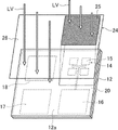
- FIG. 1 is a schematic perspective view showing an example of a laminated body according to an embodiment of the present invention.
- the laminate 10 is provided with, for example, an array antenna 14, an A / D circuit 16, a memory 17, and an ASIC (Application Specific Integrated Circuit) 18 on the substrate 12.
- the A / D circuit 16, the memory 17, and the ASIC 18 are composed of, for example, various semiconductor elements.
- the laminate 10 includes various circuits and elements of a mobile communication terminal such as a smartphone or a wireless communication module, for example, an RF (Radio Frequency) circuit, a power amplifier for transmission, and a low noise amplifier for reception. It has integrated passive elements, switches, phase shifters, etc.
- RF Radio Frequency
- the substrate 12 functions as a support for the laminated body 10, and forms the above-mentioned A / D circuit 16, memory 17, ASIC 18, and the like.
- the substrate 12 is made of polyimide, SiO 2 , or the like.
- the array antenna 14 has, for example, four antennas 15.
- the four antennas 15 are all the same.
- the configurations of the array antenna 14 and the antenna 15 are not particularly limited, and are appropriately determined according to the frequency band for transmission or reception, the polarization direction for reception, and the like. Further, the array antenna 14 has four antennas 15, but is not limited thereto. One antenna may be used instead of the array antenna 14.
- the A / D circuit 16 converts an analog signal into a digital signal, and a known AD converter is used.
- the A / D circuit 16 converts the received signal received by the array antenna 14 by radio waves into a digital signal.
- the ASIC 18 obtains the original data or signal transmitted to the array antenna 14 from the received signal converted into a digital signal. Further, the transmission data or the transmission signal is generated in the state of a digital signal.
- the function of the ASIC 18 is not particularly limited, and is appropriately determined according to the intended use and the like. Further, the A / D circuit 16 converts the transmission data or the transmission signal generated by the ASIC 18 into an analog signal that can be transmitted by the array antenna 14.
- the memory 17 stores the transmission data or transmission signal generated in the above-mentioned ASIC 18, the digital signal received signal received by the array antenna 14, and the like.
- the memory 17 for example, a volatile memory of DRAM (Dynamic Random Access Memory) is used, but HBM (High Bandwidth Memory) is preferable.
- DRAM Dynamic Random Access Memory
- HBM High Bandwidth Memory
- the magnetic material pattern portion 20 is arranged at least in a part of the periphery of the array antenna 14 so as to be separated from the array antenna 14 on the substrate 12.
- the magnetic pattern unit 20 absorbs electromagnetic waves transmitted from the array antenna 14 or received by the array antenna 14.
- the magnetic pattern portion 20 of FIG. 1 is provided on the surface 12a of the substrate 12 so as to cover the A / D circuit 16, the memory 17, and the ASIC 18 except for the array antenna 14.
- the width of the magnetic pattern portion 20 may be an integral multiple of 1/4 of the wavelength of the electromagnetic wave transmitted or received by the array antenna 14 in order to absorb the electromagnetic wave transmitted or received by the array antenna 14 from the array antenna 14. preferable.
- the magnetic pattern portion 20 suppresses electromagnetic interference of the A / D circuit 16, the memory 17, and the ASIC 18 due to the electromagnetic waves emitted by the array antenna 14. As a result, the A / D circuit 16, the memory 17, and the ASIC 18 are not hindered from normal operation, and malfunctions are suppressed.
- the directivity of the antenna output is strengthened, and by further inserting the magnetic material into the layered body of the wafer level package as a structure, the laminated body can be made of the laminated body. High integration and high performance are also possible.
- a composition containing magnetic particles and a polymerizable compound is applied onto a substrate on which an antenna is arranged to form a composition layer, and the composition layer is exposed and developed to obtain a magnetic pattern. It has a step of forming a portion.
- 2 and 3 are schematic perspective views showing a manufacturing method of an example of the laminated body of the embodiment of the present invention in the order of processes. In FIGS. 2 and 3, the same components as those shown in FIG. 1 are designated by the same reference numerals, and detailed description thereof will be omitted.
- an array antenna 14, an A / D circuit 16, a memory 17, and an ASIC 18 are prepared on a substrate 12.
- the array antenna 14, the A / D circuit 16, the memory 17, and the ASIC 18 are formed on the substrate 12 by using various known manufacturing methods of semiconductor devices.
- the composition layer 22 covering the entire surface 12a of the substrate 12 is formed.
- the array antenna 14, the A / D circuit 16, the memory 17, and the ASIC 18 are covered with the composition layer 22.
- the composition layer 22 is a negative type, and the unexposed portion is removed by the development process.
- the photomask 24 shown in FIG. 3 is arranged.
- the photomask 24 is provided with, for example, a mask portion 25 in a region where the array antenna 14 is arranged and a region corresponding to the magnetic material pattern portion 20.
- the exposure light Lv that exposes the composition layer 22 is transmitted through the region 26 other than the mask portion 25.
- the mask portion 25 blocks the exposure light Lv.
- the composition layer 22 exposed using the photomask 24 shown in FIG. 3 is a negative type, and the unexposed portion is removed by the development process. That is, the array antenna 14 and the magnetic material pattern portion 20 are unexposed portions.
- the composition layer 22 is of the positive type, the exposed portion is removed by the development process, so that the light-shielding region of the photomask 24 is opposite to that of the photomask 24 shown in FIG.
- the photomask 24 is arranged on the substrate 12 and exposed, and then developed to form a magnetic pattern portion 20 (see FIG. 1). As a result, the laminated body 10 shown in FIG. 1 is obtained.
- the magnetic material pattern portion 20 (see FIG. 1) can be formed by the exposure treatment and the development treatment, and a highly integrated and high-performance laminated body can be easily manufactured. Conventionally, it is a magnetic material that maximizes ⁇ '', which represents electromagnetic wave absorption, out of the real part ( ⁇ ') of magnetic permeability and the complex part ( ⁇ '') of magnetic permeability, and is a communication standard 5G (Generation). ), A non-photosensitive material that absorbs electromagnetic waves of 28 GHz, 47 GHz, or 78 GHz is used.
- the size of the magnetic material is made an integral multiple of 1/4 of the wavelength of the electromagnetic wave transmitted from or received by the antenna, which enables electromagnetic wave absorption by resonance and saves space. Therefore, the shielding efficiency can be greatly improved.
- the magnetic pattern portion is arranged at least a part of the periphery of the antenna so as to be separated from the antenna on the substrate 12, the surface 12a of the substrate 12 except for the array antenna 14 shown in FIG. 1
- the magnetic material pattern portion 20 provided so as to cover the A / D circuit 16, the memory 17, and the ASIC 18 is not particularly limited.
- various patterns can be used, and the magnetic material pattern portion may be in the form of an FSS (Frequency Selective Surface) element.
- the FSS element shape is composed of a combination of lines and spaces that are integral multiples of the wavelength of the electromagnetic wave transmitted from or received by the antenna.
- the fact that the magnetic material pattern portion 20 is arranged apart from the antenna on the substrate 12 means that the antenna and the magnetic material pattern portion 20 are provided on the same surface of the substrate, and the antenna is provided on the surface of the substrate. Is not provided, and the magnetic material pattern portion is not provided on the back surface of the substrate. If there is a step on the substrate, if the substrate is bent, or if another layer such as an adhesion layer is included between the substrate and the magnetic pattern portion, it is regarded as the same surface.
- the magnetic pattern portion is arranged at least a part of the periphery of the antenna, but it is preferable that the magnetic pattern portion is arranged at 120 ° or more of 360 ° in the horizontal direction centered on the antenna.
- the magnetic pattern portion preferably exists on the entire circumference of the antenna in order to shield the electromagnetic wave from the antenna.
- the entire circumference of the antenna is 337.5 ° or more of 360 ° in the horizontal direction centered on the antenna.
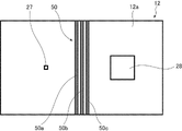
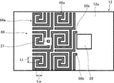
- FIGS. 4 to 30 are schematic views showing the first to 27th examples of the magnetic material pattern portion of the laminated body of the embodiment of the present invention.
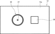
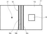
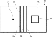
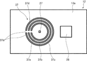
- a magnetic material pattern portion is arranged between one antenna 27 and one semiconductor element 28 on the substrate 12.
- a single annular magnetic material pattern portion 30 that surrounds the entire circumference of the antenna 27 is provided.
- the magnetic pattern portion 30 is arranged on the entire circumference of the antenna 27 and is arranged in an annular shape.
- the width of the magnetic pattern portion 30 is, for example, 1/4 of the wavelength of the electromagnetic wave transmitted from the antenna 27 or received by the antenna 27. Therefore, the width is appropriately set depending on the wavelength of the electromagnetic wave transmitted from the antenna 27 or received by the antenna 27. If the frequency of the electromagnetic wave transmitted from the antenna 27 or received by the antenna 27 is, for example, 60 GHz, the wavelength of the electromagnetic wave is about 5.00 mm, and the width of the magnetic pattern portion 30 is about 1.25 mm.
- the width of the magnetic pattern portion 30 may be an integral multiple of 2 or more of 1/4 of the wavelength of the electromagnetic wave transmitted from the antenna 27 or received by the antenna 27, and is ⁇ 10% with respect to the value of the predetermined width. Tolerable to some extent.
- a double annular magnetic material pattern portion 32 that surrounds the entire circumference of the antenna 27 is provided.
- the magnetic pattern portion 32 is arranged on the entire circumference of the antenna 27 and is arranged in a double annular shape, and is an annular shape that captures the entire circumference of the annular first pattern portion 32a and the first pattern portion 32a. It has a second pattern portion 32b.
- the first pattern portion 32a and the second pattern portion 32b are arranged concentrically.
- the first pattern portion 32a and the second pattern portion 32b have the same width, and are, for example, 1/4 of the wavelength of the electromagnetic wave transmitted from the antenna 27 or received by the antenna 27.
- the width of the first pattern portion 32a and the second pattern portion 32b is about 1.25 mm.
- the distance between the first pattern portion 32a and the second pattern portion 32b is also, for example, an integral multiple of 1/4 of the wavelength of the electromagnetic wave transmitted from the antenna 27 or received by the antenna 27.
- the width and interval described above may be an integral multiple of 2 or more of 1/4 of the wavelength of the electromagnetic wave transmitted from the antenna 27 or received by the antenna 27, and are allowed about ⁇ 10% with respect to the value of the specified width. do.
- a triple annular magnetic material pattern portion 34 that surrounds the entire circumference of the antenna 27 is provided.
- the magnetic pattern portion 34 is arranged on the entire circumference of the antenna 27 and is arranged in a triple annular shape, and is an annular shape that captures the first pattern portion 34a of the annular shape and the entire circumference of the first pattern portion 34a. It has a second pattern portion 34b and an annular third pattern portion 34c that captures the entire circumference of the second pattern portion 34b.
- the first pattern portion 34a, the second pattern portion 34b, and the third pattern portion 34c have the same width and are arranged concentrically.
- the width of the first pattern portion 32a, the width of the second pattern portion 32b, and the width of the third pattern portion 34c are, for example, 1/4 of the wavelength of the electromagnetic wave transmitted from the antenna 27 or received by the antenna 27. In this case, for example, if the frequency of the electromagnetic wave transmitted or received is 60 GHz, the width of the first pattern portion 32a, the width of the second pattern portion 32b, and the width of the third pattern portion 34c are about 1.25 mm. Further, the distance between the first pattern unit 32a, the second pattern unit 32b, and the third pattern unit 34c is also, for example, 1/4 of the wavelength of the electromagnetic wave transmitted from the antenna 27 or received by the antenna 27.
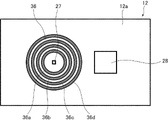
- a quadruple annular magnetic material pattern portion 36 that surrounds the entire circumference of the antenna 27 is provided.
- the magnetic pattern portion 36 is arranged on the entire circumference of the antenna 27 and is arranged in a quadruple annular shape, and is an annular shape that captures the entire circumference of the annular first pattern portion 36a and the first pattern portion 36a. It has a second pattern portion 36b, an annular third pattern portion 36c that captures the entire circumference of the second pattern portion 36b, and an annular fourth pattern portion 36d that captures the entire circumference of the third pattern portion 36c. ..
- the first pattern portion 36a, the second pattern portion 36b, the third pattern portion 36c, and the fourth pattern portion 36d have the same width and are arranged concentrically.
- the width of the first pattern portion 36a, the width of the second pattern portion 36b, the width of the third pattern portion 36c, and the width of the fourth pattern portion 36d are, for example, 1 of the wavelength of the electromagnetic wave transmitted from the antenna 27 or received by the antenna 27. / 4.
- the width of the first pattern portion 32a, the width of the second pattern portion 32b, the width of the third pattern portion 34c, and the width of the fourth pattern portion 36d are , Approximately 1.25 mm.
- the distance between the first pattern unit 32a, the second pattern unit 32b, the third pattern unit 34c, and the fourth pattern unit 36d is also, for example, 1/4 of the wavelength of the electromagnetic wave transmitted from the antenna 27 or received by the antenna 27.
- the width and spacing of the above-mentioned pattern portions in FIGS. 5 to 7 may be 1/4 of the wavelength of the electromagnetic wave transmitted or received by the antenna 27, and may be an integral multiple of 2 or more.
- 4 to 7 are all annular magnetic material pattern portions that surround the entire circumference of the antenna, but the quadruple annular magnetic material pattern portion shown in FIG. 7 is preferable from the viewpoint of the ability to shield electromagnetic waves. ..
- the width of each pattern portion and the interval between the pattern portions are both 1 of the wavelength of the electromagnetic wave transmitted from the antenna 27 or received by the antenna 27, as described above. / 4.
- the width of each of the above-mentioned pattern portions and the interval between the pattern portions are about 1.25 mm.
- the width and spacing of each pattern portion may be an integral multiple of 1/4 of the wavelength of the electromagnetic wave transmitted from the antenna 27 or received by the antenna 27. Allow about ⁇ 10% of the width value.
- a magnetic material pattern portion 38 that surrounds the entire circumference of the antenna 27 is provided.
- the magnetic pattern portion 38 is arranged on the entire circumference of the antenna 27, has a triple triangular pattern, and has a triangular shape that captures the entire circumference of the triangular first pattern portion 38a and the first pattern portion 38a. It has a second pattern portion 38b and a triangular third pattern portion 38c that captures the entire circumference of the second pattern portion 38b.
- the first pattern portion 38a, the second pattern portion 38b, and the third pattern portion 38c have the same width and are similar figures.
- the first pattern portion 38a, the second pattern portion 38b, and the third pattern portion 38c are arranged so that their centers of gravity coincide with each other.
- a magnetic material pattern portion 40 that surrounds the entire circumference of the antenna 27 is provided.
- the magnetic pattern portion 40 is arranged on the entire circumference of the antenna 27, has a triple quadrangular pattern, and captures the quadrangular first pattern portion 40a and the entire circumference of the first pattern portion 40a. It has a second pattern portion 40b and a quadrangular third pattern portion 40c that captures the entire circumference of the second pattern portion 40b.
- the first pattern portion 40a, the second pattern portion 40b, and the third pattern portion 40c have similar figures and are arranged so that their centers are aligned. The center is the point where the two diagonal lines intersect.
- a magnetic material pattern portion 42 that surrounds the entire circumference of the antenna 27 is provided.
- the magnetic pattern portion 42 is arranged on the entire circumference of the antenna 27, has a triple hexagonal pattern, and has a hexagonal shape that captures the entire circumference of the hexagonal first pattern portion 42a and the first pattern portion 42a. It has a second pattern portion 42b and a hexagonal third pattern portion 42c that captures the entire circumference of the second pattern portion 42b.
- the first pattern portion 42a, the second pattern portion 42b, and the third pattern portion 42c have the same width and are similar figures.
- the first pattern portion 42a, the second pattern portion 42b, and the third pattern portion 42c are arranged so that their centers are aligned with each other.
- a magnetic material pattern portion 44 that surrounds the entire circumference of the antenna 27 is provided.
- the magnetic pattern portion 44 is arranged on the entire circumference of the antenna 27, has a triple octagonal pattern, and has an octagonal shape that captures the entire circumference of the octagonal first pattern portion 44a and the first pattern portion 44a. It has a second pattern portion 44b and an octagonal third pattern portion 44c that captures the entire circumference of the second pattern portion 44b.
- the first pattern portion 44a, the second pattern portion 44b, and the third pattern portion 44c have the same width and are similar figures.
- the first pattern portion 44a, the second pattern portion 44b, and the third pattern portion 44c are arranged so that their centers are aligned with each other.
- a magnetic material pattern portion 46 that surrounds the entire circumference of the antenna 27 is provided.
- the magnetic pattern portion 46 is arranged on the entire circumference of the antenna 27, has a triple dodecagonal pattern, and captures the dodecagonal first pattern portion 46a and the entire circumference of the first pattern portion 46a. It has a square-shaped second pattern portion 46b and a ten-shaped third pattern portion 46c that captures the entire circumference of the second pattern portion 46b.
- the first pattern portion 46a, the second pattern portion 46b, and the third pattern portion 46c have the same width and are similar figures.
- the first pattern portion 46a, the second pattern portion 46b, and the third pattern portion 46c are arranged so that their centers are aligned with each other.
- FIGS. 8 to 12 described above each have a triple polygonal magnetic material pattern portion.
- the polygons shown in FIGS. 8 to 10 having a triangular outer shape, a quadrangle, and a hexagon suppress the concentration of reflected electromagnetic waves, and emit electromagnetic waves more than the triple annular magnetic material pattern portion shown in FIG. High ability to shield.
- FIG. 10 shows an octagonal outer shape
- FIG. 11 shows an outer shape of a decagon
- the outer shape is close to a circle
- the ability to shield electromagnetic waves is a triple annular magnetic material pattern portion shown in FIG. Is about the same as.
- a magnetic material pattern portion 48 that surrounds the entire circumference of the antenna 27 is provided.
- the magnetic pattern portion 48 is provided on the entire circumference of the antenna 27, and has a linear first pattern portion 48a, a linear second pattern portion 48b, and a linear third pattern portion 48c. , These are arranged parallel to each other. Further, the first pattern portion 48a, the second pattern portion 48b, and the third pattern portion 48c are arranged so as to face each other with the antenna 27 interposed therebetween.
- a linear shape extending in a direction orthogonal to the first pattern portion 48a, the second pattern portion 48b, and the third pattern portion 48c at both ends of the first pattern portion 48a, the second pattern portion 48b, and the third pattern portion 48c, respectively.
- the fourth pattern portion 48d is arranged.
- the linear fifth pattern portion 48e and the linear sixth pattern portion 48f are arranged in parallel with each other with a gap from the fourth pattern portion 48d. None of the first pattern portion 48a to the sixth pattern portion 48f is connected to other pattern portions. Further, the first pattern portion 48a to the sixth pattern portion 48f have the same width.
- the magnetic material pattern portion 48 is a pattern in which three lines and spaces are combined. For example, when two or more parallel rods are connected like a tuning fork, energy is transmitted and resonates, but the first pattern portion 48a to the sixth pattern portion 48f are all connected to other pattern portions. Since it is not, resonance is suppressed and a high ability to shield electromagnetic waves can be obtained.
- the width of the first pattern portion 48a to the sixth pattern portion 48f is, for example, 1/4 of the wavelength of the electromagnetic wave transmitted from the antenna 27 or received by the antenna 27. In this case, for example, if the frequency of the electromagnetic wave transmitted or received is 60 GHz, it is about 1.25 mm. Further, the interval between the first pattern portion 48a and the sixth pattern portion 48f is also, for example, 1/4 of the wavelength of the electromagnetic wave transmitted from the antenna 27 or received by the antenna 27.
- the width and interval described above may be an integral multiple of 2 or more of the wavelength 1/4 of the electromagnetic wave transmitted or received by the antenna 27, and are allowed to be about ⁇ 10% with respect to the value of the specified width.
- a magnetic material pattern portion 50 is provided between the antenna 27 and the semiconductor element 28 on the substrate 12.
- the magnetic pattern portion 50 is provided on one side of the antenna 27.
- a linear first pattern portion 50a, a linear second pattern portion 50b, and a linear third pattern portion 50c are arranged at intervals in parallel with each other.
- the first pattern portion 50a, the second pattern portion 50b, and the third pattern portion 50c have the same width, and the spacing is the same as the width.
- the width of the first pattern portion 50a, the width of the second pattern portion 50b, and the width of the third pattern portion 50c are, for example, 1/4 of the wavelength of the electromagnetic wave transmitted from the antenna 27 or received by the antenna 27, and are, for example, transmitted.
- the frequency of the received electromagnetic wave is 60 GHz, it is about 1.25 mm.
- the interval is also, for example, 1/4 of the wavelength of the electromagnetic wave transmitted from the antenna 27 or received by the antenna 27.
- the width and spacing described above may be an integral multiple of 2 or more of 1/4 of the wavelength of the electromagnetic wave transmitted from the antenna 27 or received by the antenna 27.
- the magnetic material pattern portion 50 of FIG. 15 is different from the magnetic material pattern portion 50 of FIG. 14 except that the distance between the first pattern portion 50a, the second pattern portion 50b, and the third pattern portion 50c is different. It has the same configuration as that of FIG.
- the distance between the first pattern portion 50a, the second pattern portion 50b, and the third pattern portion 50c is twice the width of the first pattern portion 50a, the second pattern portion 50b, and the third pattern portion 50c.
- the interval is, for example, twice the wavelength of the electromagnetic wave transmitted from the antenna 27 or received by the antenna 27.
- the magnetic material pattern portion 50 of FIG. 16 is different from the magnetic material pattern portion 50 of FIG. 14 except that the distance between the first pattern portion 50a, the second pattern portion 50b, and the third pattern portion 50c is different. It has the same configuration as that of FIG.
- the distance between the first pattern portion 50a, the second pattern portion 50b, and the third pattern portion 50c is three times the width of the first pattern portion 50a, the second pattern portion 50b, and the third pattern portion 50c.
- the interval is, for example, three times the wavelength of the electromagnetic wave transmitted from the antenna 27 or received by the antenna 27.
- the magnetic material pattern portion 50 of FIG. 17 is different from the magnetic material pattern portion 50 of FIG.
- the distance between the first pattern portion 50a, the second pattern portion 50b, and the third pattern portion 50c is different. It has the same configuration as that of FIG.
- the distance between the first pattern portion 50a, the second pattern portion 50b, and the third pattern portion 50c is four times the width of the first pattern portion 50a, the second pattern portion 50b, and the third pattern portion 50c.
- the interval is, for example, four times the wavelength of the electromagnetic wave transmitted from the antenna 27 or received by the antenna 27. 14 to 17 are so-called line-and-space patterns.
- the relationship between the distance between the first pattern portion 50a, the second pattern portion 50b, and the third pattern portion 50c and the width of the first pattern portion 50a, the second pattern portion 50b, and the third pattern portion 50c is
- the interval may be 5 times, 6 times, or 7 times the width.
- the interval may be, for example, 5 times, 6 times, or 7 times the wavelength of the electromagnetic wave transmitted from the antenna 27 or received by the antenna 27.
- the upper limit of the L / S ratio is appropriately determined by the size of the region in which the magnetic pattern is arranged, and the upper limit of the L / S ratio is about 10.
- the width and spacing of each pattern portion are ⁇ with respect to the value of the defined width. Allow about 10%.
- a magnetic material pattern portion 52 that surrounds the antenna 27 is provided.
- the magnetic material pattern portion 52 has, for example, four annular pattern portions 53 in which a part is cut out.
- the width of the notched portion 53a of the pattern portion 53 is, for example, 1/4 of the wavelength of the electromagnetic wave transmitted from the antenna 27 or received by the antenna 27. In this case, for example, if the frequency of the electromagnetic wave transmitted or received is 60 GHz, the width of the notch 53a is about 1.25 mm.
- the pattern portion 53 is arranged around the antenna 27 at intervals of 90 ° with the notch portion 53a facing the antenna 27.
- the pattern portion 53 is arranged on a virtual square 53b.
- the distance between the centers of the opposing pattern portions 53 is, for example, 14 mm.
- the width of the notch 53a may be an integral multiple of 2 or more of 1/4 of the wavelength of the electromagnetic wave transmitted from the antenna 27 or received by the antenna 27. Since the reflection of the electromagnetic wave is canceled by the notch 53a, the ability to shield the electromagnetic wave is higher than that of the configuration of the annular pattern portion having no notch.
- the magnetic pattern portion 54 in FIG. 19 has a different number of pattern portions 53 as compared with FIG. 18, and has, for example, eight.
- the pattern portion 53 is arranged at the corners of the four pattern portions 53 of the magnetic material pattern portion 52 of FIG. The entire circumference of the antenna 27 is surrounded by the pattern portion 53.
- the pattern portions 53 provided at the corners of the four pattern portions 53 of the magnetic material pattern portion 52 of FIG. 18 are arranged so that the cutout portions 53a are in contact with the other pattern portions 53.
- the magnetic material pattern portion 54 shown in FIG. 19 has a higher electromagnetic wave shielding effect than the magnetic material pattern portion 52 shown in FIG. 18, and is more preferable.
- a magnetic material pattern portion 56 is provided between the antenna 27 and the semiconductor element 28 on the substrate 12.
- the pattern portions 53 are arranged in a row on the line CL, for example, and the notch portions 53a are directed toward the antenna 27 side. Further, the antenna 27 and the line CL on which the pattern portion 53 is arranged are separated by a distance of Lc.
- the magnetic material pattern portion 58 of FIG. 21 has the same configuration as that of the magnetic material pattern portion 56 shown in FIG. 20, except that the configuration of the pattern portion 58a is different.
- the pattern portion 58a is annular and is not provided with a notch portion 53a.
- the magnetic material pattern portion 60 of FIG. 22 has the same configuration as that of the magnetic material pattern portion 56 shown in FIG.
- the pattern portion 60a has a disk shape and is not provided with a notch portion 53a.
- the magnetic material pattern portion 37 of FIG. 23 has the same configuration as that of the magnetic material pattern portion 36 of FIG. 6, except that the configurations of the first pattern portion 37a, the second pattern portion 37b, and the third pattern portion 37c are different. Is. Notches 37d are provided in the first pattern portion 37a, the second pattern portion 37b, and the third pattern portion 37c, respectively.
- the first pattern portion 37a, the second pattern portion 37b, and the third pattern portion 37c are arranged concentrically with the cutout portions 37d matching each other.
- the notch 37d is arranged toward the opposite side of the semiconductor element 28.
- the cutout portion 37d has the same configuration as the above-mentioned cutout portion 53a. Further, the magnetic pattern portion 37 of FIG. 23 has a first pattern portion 37a, a second pattern portion 37b, and a third pattern portion 37c, but the present invention is not limited to this, and the first pattern portion 37a alone is not limited to this. good.
- the magnetic pattern portion 62 of FIG. 24 has a pattern using fractals and has an FSS element-like configuration.
- the magnetic material pattern portion 62 for example, four H-shaped pattern portions 62a are arranged in the same direction, and the pattern portion 62b connecting the vertically arranged pattern portions 62a and the pattern portion 62b are connected to each other. It has a pattern portion 62c.
- the pattern portion 62a is composed of sub-pattern portions 62d to 62f.
- the pattern portion 62a, the pattern portion 62b, and the pattern portion 62c form a constituent pattern portion 62g.
- the magnetic pattern portion 62 has two constituent pattern portions 62g.
- the magnetic pattern portion 62 has a fractal structure, and the number of combinations in which the pattern portion is repeated three times increases, and the ability to shield electromagnetic waves increases.
- the width of each of the pattern unit 62a, the pattern unit 62b, the pattern unit 62c, and the sub-pattern unit 62d is, for example, an integral multiple of 1/4 of the wavelength of the electromagnetic wave transmitted from the antenna 27 or received by the antenna 27.
- the distance between the pattern portions in the extending direction of the pattern portion 62c is, for example, an integral multiple of 1/4 of the wavelength of the electromagnetic wave transmitted from the antenna 27 or received by the antenna 27.
- the sub-pattern portion 62f extending from the antenna 27 of the pattern portion 62a toward the semiconductor element 28 is 6 times the wavelength, and is 6 times the wavelength, and the sub-pattern portion 62e extending in the direction orthogonal to the above-mentioned heading direction. Is 5 times the wavelength, and the sub-pattern portion 62e is 3 times the wavelength.
- the pattern portion 62b is 10 times the wavelength, and the pattern portion 62c is 11 times the wavelength 1/4.
- the magnetic material pattern portion 64 of FIG. 25 has a pattern using a space-filling curve, and has an FSS element-like configuration.
- the magnetic pattern portion 64 is a pattern having a recursive structure using a Hilbert curve.
- the width of the magnetic pattern portion 64 is, for example, an integral multiple of 1/4 of the wavelength of the electromagnetic wave transmitted from the antenna 27 or received by the antenna 27.
- the distance between the magnetic material pattern portions 64 in the direction from the antenna 27 toward the semiconductor element 28, that is, the space of the magnetic material pattern portion 64 is, for example, 1/4 of the wavelength of the electromagnetic wave transmitted from the antenna 27 or received by the antenna 27. Is an integral multiple of.
- the magnetic material pattern portion 64 has, for example, a length Lt of 3 times the wavelength and a length Lw of 3 times the wavelength.
- the magnetic pattern portion 66 of FIG. 26 has a spiral pattern portion 66a and a pattern portion 66b that connects the spiral pattern portions 66a to each other.
- six spiral pattern portions 66a are arranged in one row, three in a total of two rows.
- the spiral pattern portion 66a and the pattern portion 66b have, for example, the same width, and the width thereof is, for example, an integral multiple of 1/4 of the wavelength of the electromagnetic wave transmitted from the antenna 27 or received by the antenna 27.
- the magnetic material pattern portion 66 has an FSS element-like structure.
- the distance between the magnetic material pattern portions 66 in the direction from the antenna 27 toward the semiconductor element 28, that is, the space of the magnetic material pattern portion 66 is 1/4 of the wavelength of the electromagnetic wave transmitted from the antenna 27 or received by the antenna 27, for example. Is an integral multiple of.
- the magnetic material pattern portion 66 has, for example, a length Lt of 3 times the wavelength and a length Lw of 3 times the wavelength.
- the magnetic pattern portion 68 of FIG. 27 has a pattern using fractals.
- the magnetic material pattern portion 68 has a pattern portion 68a and a pattern portion 68b connecting the pattern portions 68a arranged apart from each other.
- the pattern portions 68a are arranged in different directions, and the pattern portions 68a arranged to face each other are connected to each other.
- the separated pattern portions 68a are connected by the pattern portions 68b as described above.
- the magnetic material pattern portion 68 has an FSS element-like structure.
- the pattern portion 68a and the pattern portion 68b have, for example, the same width, and the width is an integral multiple of 1/4 of the wavelength of the electromagnetic wave transmitted from the antenna 27 or received by the antenna 27.
- the distance between the magnetic material pattern portions 68 in the direction from the antenna 27 toward the semiconductor element 28, that is, the space of the magnetic material pattern portion 68 is, for example, 1/4 of the wavelength of the electromagnetic wave transmitted from the antenna 27 or received by the antenna 27. Is an integral multiple of.
- the magnetic material pattern portion 68 has, for example, a length Lt of 3 times the wavelength and a length Lw of 3 times the wavelength.
- the magnetic pattern portion 69 of FIG. 28 is a pattern having an opening 69a in the portion of the antenna 27.
- the magnetic pattern portion 70 of FIG. 29 has a plurality of hexagonal pattern portions 70a.
- the magnetic material pattern portion 70 is a honeycomb-shaped pattern.
- Each pattern portion 70a has a hexagonal opening 70b.
- the hexagonal pattern portion 70a is arranged on the surface 12a of the substrate 12 in a two-dimensional close-packed manner.
- the width of the hexagonal pattern portion 70a is an integral multiple of 1/4 of the wavelength of the electromagnetic wave transmitted from the antenna 27 or received by the antenna 27.
- the magnetic material pattern portion 70 has, for example, a length Ld that is three times a wavelength of 1/4. In FIG.
- the hexagonal pattern portion 70a is used, but the present invention is not limited to this, and may be a regular shape pattern portion, a rectangular pattern portion, and a triangular pattern portion, and further. It may be a pattern portion in which an irregularly shaped opening region such as a Voronoi pattern is irregularly defined.
- the magnetic pattern portion 72 of FIG. 30 is, for example, a pattern having a cross-shaped opening 72a.
- the magnetic pattern portion 72 of FIG. 30 also has an FSS element-like structure.
- the pattern portion 72b excluding the opening 72a has the width in the direction from the antenna 27 toward the semiconductor element 28, the length in the above-mentioned direction, and the length in the direction orthogonal to the above-mentioned direction.
- both are integral multiples of 1/4 of the wavelength of the electromagnetic wave transmitted from the antenna 27 or received by the antenna 27.
- the width of the cross-shaped opening 72a is also an integral multiple of 1/4 of the wavelength of the electromagnetic wave transmitted from the antenna 27 or received by the antenna 27.
- the width of the cross-shaped opening 72a is the length in the direction orthogonal to the direction in which the opening 72a extends.
- the length Lf is 9 times the wavelength
- the length Lg is 9 times the wavelength 1/4
- the length Lh is 3 times the wavelength 1/4. It is double.
- the shape of the opening 72a is not limited to a cross as long as the dimensions of each part are an integral multiple of 1/4 of the wavelength of the electromagnetic wave transmitted from the antenna 27 or received by the antenna 27 as described above.
- the thickness of the magnetic material pattern portion is not particularly limited as long as it is not an integral multiple of 1/4 of the wavelength of the electromagnetic wave transmitted from the antenna 27 or received by the antenna 27. do not have.
- the thickness of the magnetic pattern portion is preferably 300 ⁇ m or less from the viewpoint of pattern formation. Further, when the thickness of the magnetic material pattern portion is 300 ⁇ m or less, the height of the laminated body can be reduced.
- the antenna is not particularly limited, and the following antennas are exemplified.
- ⁇ antenna Various antennas used in the communication standard 5G (Generation) using a frequency band of 28 GHz to 80 GHz can be used.
- the antenna for example, a patch antenna, a dipole antenna, or a phased array antenna can be used.
- the antenna is made of, for example, copper or aluminum.
- the thickness of the antenna is preferably 20 to 50 ⁇ m.
- a printed circuit board such as Flame Retardant Type 1 to Type 5 (FR-1 to FR-5) is used, the thickness of the copper wiring is determined by the standard, and the thickness of the antenna is also the thickness of the copper wiring. Same as.
- the thickness of the antenna may be based on the thickness of the copper foil of the copper-clad laminate specified in JIS (Japanese Industrial Standards) C 6484: 2005 (see Table 6 etc. of JIS C 6484: 2005). .. Further, when the antenna is formed of copper by electrolytic plating, the thickness of the antenna is preferably a film thickness that can be formed by electrolytic plating.
- the semiconductor element is not particularly limited, and is, for example, a logic LSI (Large Scale Integration) (for example, ASIC (Application Specific Integrated Circuit), FPGA (Field Programmable Gate Array), ASSP (Application Specific Standard Product), etc.).
- LSI Large Scale Integration
- ASIC Application Specific Integrated Circuit
- FPGA Field Programmable Gate Array
- ASSP Application Specific Standard Product
- Microprocessor for example, CPU (Central Processing Unit), GPU (Graphics Processing Unit), etc.), memory (for example, DRAM (Dynamic Random Access Memory), HMC (Hybrid Memory Cube), MRAM (Magnetic RAM) and PCM (Phase-Change Memory), ReRAM (Resistive RAM: Resistive Random Memory), FeRAM (Ferroelectric RAM: Ferroelectric RAM), Flash Memory (NAND (Not AND) Flash), etc.), Power Devices, Analog IC (Integrated Circuit), (for example, DC (Direct Current) -DC (Direct Current) converter, isolated gate bipolar transistor (IGBT), etc.), A / D converter, MEMS (Micro Electro Mechanical Systems), (for example, acceleration) Sensors, pressure sensors, oscillators, gyro sensors, etc.), power amplifiers, wireless (for example, GPS (Global Positioning System), FM (Frequency Modulation), NFC (Nearfield communication), RFEM (RF Expansion Module), MMIC (Monolithic Microwave) Integrated
- the antenna-in package is a configuration in which an antenna and an FEM (Front End Module) are laminated.
- the FEM is a circuit portion of a transmission / reception end on the antenna side in a wireless circuit.
- the antenna-in package has a configuration in which at least an antenna, an A / D circuit 16, a memory 17, and an ASIC 18 are provided on a substrate, for example, as in the laminated body 10 shown in FIG. 1 described above. .. Further, it has a magnetic material pattern portion 20.
- known methods can be appropriately used for the antenna, the A / D circuit 16, the memory 17, the ASIC 18, and the like, except for the method for manufacturing the magnetic pattern portion 20.
- compositions containing magnetic particles and a polymerizable compound, and a method for producing a laminate will be described.
- various components contained in the composition will be described in detail.
- Magnetic particles contain metal atoms.
- the metal atom includes a metalloid atom such as boron, silicon, germanium, arsenic, antimony, and tellurium.
- the metal atom is an alloy containing a metal element (preferably a magnetic alloy), a metal oxide (preferably a magnetic oxide), a metal nitride (preferably a magnetic oxide), or a metal carbide (preferably a metal carbide). It may be contained in magnetic particles as a magnetic carbide).
- the content of the metal atom with respect to the total mass of the magnetic particles is preferably 50 to 100% by mass, more preferably 75 to 100% by mass, still more preferably 95 to 100% by mass.
- the metal atom is not particularly limited, but preferably contains at least one metal atom selected from the group consisting of Fe, Ni, and Co.
- the content of at least one metal atom selected from the group consisting of Fe, Ni, and Co is the total mass of the metal atoms in the magnetic particles. , 50% by mass or more is preferable, 60% by mass or more is more preferable, and 70% by mass or more is further preferable.
- the upper limit of the content is not particularly limited, and is, for example, 100% by mass or less, preferably 98% by mass or less, and more preferably 95% by mass or less.
- the magnetic particles may contain materials other than Fe, Ni, and Co, and specific examples thereof include Al, Si, S, Sc, Ti, V, Cu, Y, Mo, Rh, Pd, and Ag. , Sn, Sb, Te, Ba, Ta, W, Re, Au, Bi, La, Ce, Pr, Nd, P, Zn, Zr, Mn, Cr, Nb, Pb, Ca, B, C, N, and , O.
- the magnetic particles contain metal atoms other than Fe, Ni, and Co, it is preferable that the magnetic particles contain one or more selected from the group consisting of Si, Cr, B, and Mo.
- the magnetic particles include Fe—Co alloys (preferably permenyl), Fe—Ni alloys (for example, Permalloy), Fe—Zr alloys, Fe—Mn alloys, Fe—Si alloys, and Fe. -Al alloys, Ni—Mo alloys (preferably Super Malloy), Fe—Ni—Co alloys, Fe—Si—Cr alloys, Fe—Si—B alloys, Fe—Si—Al alloys (Fe-Si—Al alloys) Preferably, it is sentust), Fe—Si—B—C alloy, Fe—Si—B—Cr alloy, Fe—Si—B—Cr—C alloy, Fe—Co—Si—B alloy, Fe— Alloys such as Si—B—Nb alloys, Fe nanocrystalline alloys, Fe-based amorphous alloys and Co-based amorphous alloys, as well as spinel ferrites (preferably Ni—Zn-based ferrites, Mn—Zn-based ferrites) and hexagonal
- barium ferrite, magnetoplumbite type hexagonal ferrite and the like may be mentioned.
- the alloy may be amorphous.
- a substituted magnetoplumbite-type hexagonal ferrite in which a part of the iron atom of the hexagonal ferrite is replaced with an aluminum atom can be mentioned.
- a Ba-Fe-Al alloy, a Ca-Fe-Al alloy, or a Pb-Fe-Al alloy in which a part of the alloy is replaced with Ba, Ca or Pb is more preferable from the viewpoint of radio wave absorption in the high frequency band. ..
- the magnetic particles one type may be used alone, or two or more types may be used in combination.
- a surface layer may be provided on the surface of the magnetic particles.
- the magnetic particles since the magnetic particles have a surface layer, it is possible to impart functions to the magnetic particles according to the material of the surface layer.
- the surface layer include an inorganic layer or an organic layer.
- the thickness of the surface layer is not particularly limited, but 3 to 1000 nm is preferable from the viewpoint that the function of the surface layer is more exhibited.
- the average primary particle diameter of the magnetic particles is preferably 20 to 1000 nm.
- the average primary particle diameter of the magnetic particles is more preferably 20 to 500 nm from the viewpoint of dispersion in the composition and pattern resolution.
- the particle size of the primary particles of the magnetic particles was obtained by photographing the magnetic particles with a transmission electron microscope at an imaging magnification of 100,000 times and printing them on a printing paper so as to have a total magnification of 500,000 times. In a particle photograph, the contour of a particle (primary particle) is traced with a digitizer, and the diameter of a circle having the same area as the traced region (circle area phase diameter) is calculated for measurement.
- the primary particles refer to independent particles without agglomeration.
- Imaging using a transmission electron microscope shall be performed by a direct method using a transmission electron microscope at an acceleration voltage of 300 kV. Observation and measurement with a transmission electron microscope can be performed using, for example, a transmission electron microscope H-9000 manufactured by Hitachi and an image analysis software KS-400 manufactured by Carl Zeiss.
- the average primary particle diameter is calculated by arithmetically averaging the particle diameters of the primary particles of at least 100 magnetic particles measured above.
- the shape of the magnetic particles is not particularly limited, and may be plate-shaped, elliptical, spherical, or amorphous.
- the content of the magnetic particles is preferably 20 to 99% by mass, more preferably 25 to 80% by mass, still more preferably 30 to 60% by mass, based on the total mass of the composition.
- the content of the magnetic particles is preferably 30 to 99% by mass, more preferably 30 to 80% by mass, still more preferably 40 to 70% by mass, based on the total solid content of the composition.
- the total solid content of the composition means the components constituting the magnetic pattern portion excluding the solvent in the composition. If it is a component constituting the magnetic pattern portion, even if its property is liquid, it is regarded as a solid content.
- the polymerizable compound is a compound having a polymerizable group (photopolymerizable compound), for example, a compound containing an ethylenically unsaturated bond (hereinafter, also simply referred to as “ethylenically unsaturated group”), and a compound having an ethylenically unsaturated bond.
- ethylenically unsaturated group a compound having an ethylenically unsaturated bond
- An epoxy group and / or a compound having an oxetanyl group, and a compound containing an ethylenically unsaturated group is preferable.
- the composition preferably contains a small molecule compound containing an ethylenically unsaturated group as a polymerizable compound.
- the polymerizable compound is preferably a compound containing one or more ethylenically unsaturated bonds, more preferably a compound containing two or more, further preferably three or more, and particularly preferably five or more.
- the upper limit is, for example, 15 or less.
- examples of the ethylenically unsaturated group include a vinyl group, a (meth) allyl group, a (meth) acryloyl group and the like.
- the polymerizable compound for example, the compounds described in paragraph 0050 of JP-A-2008-260927 and paragraph 0040 of JP-A-2015-068893 can be used, and the above contents are described in the present specification. Be incorporated.
- the polymerizable compound may be in any chemical form such as, for example, a monomer, a prepolymer, an oligomer, a mixture thereof, and a multimer thereof.
- the polymerizable compound is preferably a (meth) acrylate compound having 3 to 15 functionalities, and more preferably a (meth) acrylate compound having 3 to 6 functionalities.
- the polymerizable compound is also preferably a compound containing one or more ethylenically unsaturated groups and having a boiling point of 100 ° C. or higher under normal pressure.
- the compounds described in paragraphs 0227 of JP2013-209760A and paragraphs 0254-0257 of JP2008-292970 can be referred to, and the contents thereof are incorporated in the present specification.
- the polymerizable compounds include dipentaerythritol triacrylate (commercially available KAYARAD D-330; manufactured by Nippon Kayaku Co., Ltd.), dipentaerythritol tetraacrylate (commercially available KAYARAD D-320; manufactured by Nippon Kayaku Co., Ltd.), and the like.
- Dipentaerythritol penta (meth) acrylate (commercially available KAYARAD D-310; manufactured by Nippon Kayaku Co., Ltd.), dipentaerythritol hexa (meth) acrylate (commercially available as KAYARAD DPHA; manufactured by Nippon Kayaku Co., Ltd.), A-DPH -12E; manufactured by Shin-Nakamura Kagaku Co., Ltd.) and structures in which these (meth) acryloyl groups are mediated by ethylene glycol residues or propylene glycol residues (for example, SR454, SR499 commercially available from Sartmer). preferable. These oligomer types can also be used.
- NK ester A-TMMT penentaerythritol tetraacrylate, manufactured by Shin-Nakamura Chemical Co., Ltd.
- KAYARAD RP-1040 penentaerythritol tetraacrylate, manufactured by Shin-Nakamura Chemical Co., Ltd.
- KAYARAD DPEA-12LT KAYARAD DPHA LT
- KAYARAD RP-3060 KAYARAD DPEA-12
- KAYARAD DPEA-12 all trade names
- the polymerizable compound may have an acid group such as a carboxylic acid group, a sulfonic acid group, and a phosphoric acid group.
- an ester of an aliphatic polyhydroxy compound and an unsaturated carboxylic acid is preferable, and an acid is obtained by reacting an unreacted hydroxyl group of the aliphatic polyhydroxy compound with a non-aromatic carboxylic acid anhydride.
- the above polymerizable compound having a group is more preferable, and in this ester, a compound in which the aliphatic polyhydroxy compound is pentaerythritol and / or dipentaerythritol is further preferable.
- the acid value of the polymerizable compound containing an acid group is preferably 0.1 to 40 mgKOH / g, more preferably 5 to 30 mgKOH / g.
- the acid value of the polymerizable compound is 0.1 mgKOH / g or more, the developing and dissolving characteristics are good, and when the acid value is 40 mgKOH / g or less, it is advantageous in production and / or handling. Furthermore, the photopolymerization performance is good and the curability is excellent.
- a compound containing a caprolactone structure is also a preferable embodiment.
- the compound containing a caprolactone structure is not particularly limited as long as the caprolactone structure is contained in the molecule, and for example, trimethylolethane, ditrimethylolethane, trimethylolpropane, ditrimethylolpropane, pentaerythritol, dipentaerythritol, tripentaerythritol, etc.
- Examples thereof include ⁇ -caprolactone-modified polyfunctional (meth) acrylate obtained by esterifying a polyhydric alcohol such as glycerin, diglycerol or trimethylolpropane with (meth) acrylic acid and ⁇ -caprolactone.
- a compound containing a caprolactone structure represented by the following formula (Z-1) is preferable.
- R 1 represents a hydrogen atom or a methyl group
- m represents a number of 1 or 2
- "*" represents a bond.
- R 1 represents a hydrogen atom or a methyl group
- "*" represents a bond
- E represents-((CH 2 ) y CH 2 O)-or-((CH 2 ) y CH (CH 3 ) O)-.
- y represents an integer from 0 to 10
- X represents a (meth) acryloyl group, a hydrogen atom, or a carboxylic acid group.
- the total number of (meth) acryloyl groups is 3 or 4
- m represents an integer of 0 to 10
- the total of each m is an integer of 0 to 40.
- the total number of (meth) acryloyl groups is 5 or 6
- n represents an integer of 0 to 10
- the total of each n is an integer of 0 to 60.
- m is preferably an integer of 0 to 6, and more preferably an integer of 0 to 4. Further, the total of each m is preferably an integer of 2 to 40, more preferably an integer of 2 to 16, and even more preferably an integer of 4 to 8.
- n is preferably an integer of 0 to 6, and more preferably an integer of 0 to 4. Further, the total of each n is preferably an integer of 3 to 60, more preferably an integer of 3 to 24, and even more preferably an integer of 6 to 12.
- the compound represented by the formula (Z-4) or the formula (Z-5) may be used alone or in combination of two or more.
- all 6 Xs are acryloyl groups
- all 6 Xs are acryloyl groups
- among the 6 Xs The embodiment in which at least one is a mixture with a compound having a hydrogen atom is preferable. With such a configuration, the developability can be further improved.
- the total content of the compound represented by the formula (Z-4) or the formula (Z-5) in the polymerizable compound is preferably 20% by mass or more, more preferably 50% by mass or more.
- a pentaerythritol derivative and / or a dipentaerythritol derivative is more preferable.
- the said polymerizable compound may contain a cardo skeleton.
- the polymerizable compound containing a cardo skeleton the polymerizable compound containing a 9,9-bisarylfluorene skeleton is preferable.
- the content of the ethylenically unsaturated group of the polymerizable compound (meaning the value obtained by dividing the number of ethylenically unsaturated groups in the polymerizable compound by the molecular weight (g / mol) of the polymerizable compound) is 5. It is preferably 0.0 mmol / g or more.
- the upper limit is not particularly limited, but is generally 20.0 mmol / g or less.
- the content of the polymerizable compound in the composition is not particularly limited, but is preferably 1 to 40% by mass, more preferably 5 to 30% by mass, and 10 to 25% by mass with respect to the total solid content of the composition. More preferred.
- the composition may contain materials other than the above-mentioned magnetic particles and the polymerizable compound.
- the composition may contain a resin.
- the resin include (meth) acrylic resin, epoxy resin, en-thiol resin, polycarbonate resin, polyether resin, polyarylate resin, polysulfone resin, polyethersulfone resin, polyphenylene resin, polyarylene ether phosphine oxide resin, and polyimide resin.
- examples thereof include polyamideimide resin, polyolefin resin, cyclic olefin resin, polyester resin, styrene resin, and phenoxy resin.
- One of these resins may be used alone, or two or more thereof may be mixed and used.
- an unsaturated double bond for example, an ethylenically unsaturated double bond
- a resin having a polymerizable group such as an epoxy group or an oxetanyl group
- a resin having an acid group, a basic group or an amide group can be mentioned.
- a resin having an acid group, a basic group or an amide group tends to exert a function as a dispersant for dispersing magnetic particles.
- the acid group include a carboxy group, a phosphoric acid group, a sulfo group, a phenolic hydroxyl group and the like, and a carboxy group is preferable.
- the basic group examples include an amino group (ammonia, a group obtained by removing one hydrogen atom from a primary amine or a secondary amine), and an imino group.
- the resin preferably has a carboxy group or an amide group.
- the acid value of the resin is preferably 10 to 500 mgKOH / g, more preferably 30 to 400 mgKOH / g.
- the resin it is preferable to use a resin having a solubility in a solvent of 10 g / L or more because the dispersibility of the resin in the composition is improved, and it is more preferable to use a resin having a solubility in a solvent of 20 g / L or more.
- the upper limit of the solubility of the resin in the solvent is preferably 2000 g / L or less, more preferably 1000 g / L or less.
- the solubility of the resin in the solvent means the amount (g) of the resin dissolved in 1 L of the solvent at 25 ° C.
- the content of the resin is preferably 0.1 to 30% by mass, more preferably 1 to 25% by mass, and even more preferably 5 to 20% by mass with respect to the total mass of the composition.
- One of the preferred embodiments of the resin is a resin (hereinafter, also referred to as “dispersed resin”) that functions as a dispersant for dispersing magnetic particles in the composition.
- dispersed resin a resin that functions as a dispersant for dispersing magnetic particles in the composition.
- the dispersed resin examples include a resin having a repeating unit containing a graft chain (hereinafter, also referred to as “resin A”).
- resin A can be used for purposes other than exerting the function as a dispersant.
- the content of the resin A is preferably 0.1 to 30% by mass, preferably 0.5 to 20% by mass, based on the total mass of the composition, from the viewpoint that the effect of the present invention is more excellent.
- the mass% is more preferable, and 1 to 10% by mass is further preferable.
- the graft chain preferably has 40 to 10000 atoms excluding hydrogen atoms, more preferably 50 to 2000 atoms excluding hydrogen atoms, and has an atomic number excluding hydrogen atoms. It is more preferably 60 to 500.
- the graft chain indicates from the root of the main chain (atom bonded to the main chain in a group branched from the main chain) to the end of the group branched from the main chain.
- the graft chain preferably contains a polymer structure, and examples of such a polymer structure include a poly (meth) acrylate structure (for example, a poly (meth) acrylic structure), a polyester structure, a polyurethane structure, and a polyurea. Examples include a structure, a polyamide structure, and a polyether structure.
- the graft chain is selected from the group consisting of polyester structure, polyether structure, and poly (meth) acrylate structure. It is preferably a graft chain containing at least one of these, and more preferably a graft chain containing at least one of a polyester structure and a polyether structure.
- the resin A may be a resin obtained by using a macromonomer containing a graft chain (a monomer having a polymer structure and binding to a main chain to form a graft chain).
- the macromonomer containing a graft chain (a monomer having a polymer structure and binding to a main chain to form a graft chain) is not particularly limited, but a macromonomer containing a reactive double bond group can be preferably used. ..
- Suitable macromonomers corresponding to the repeating unit containing the above-mentioned graft chain and preferably used for the synthesis of resin A include AA-6, AA-10, AB-6, AS-6, AN-6, and AW-6. , AA-714, AY-707, AY-714, AK-5, AK-30, and AK-32 (all trade names, manufactured by Toagosei Co., Ltd.), and Blemmer PP-100, Blemmer PP-500, Blemmer PP-800, Blemmer PP-1000, Blemmer 55-PET-800, Blemmer PME-4000, Blemmer PSE-400, Blemmer PSE-1300, and Blemmer 43PAPE-600B (all trade names, manufactured by Nichiyu Co., Ltd.) Used.
- the resin A preferably contains at least one structure selected from the group consisting of methyl polyacrylic acid, methyl polymethacrylate, and cyclic or chain polyester, and methyl polyacrylate, polymethyl methacrylate, and the like. And, it is more preferable to include at least one structure selected from the group consisting of chain polyester, and the group consisting of a methyl polyacrylate structure, a polymethyl methacrylate structure, a polycaprolactone structure, and a polyvalerolactone structure. It is more preferred to include at least one more selected structure.
- the resin A may contain one of the above structures alone, or may contain a plurality of these structures.
- the polycaprolactone structure refers to a structure containing a ring-opened structure of ⁇ -caprolactone as a repeating unit.
- the polyvalerolactone structure refers to a structure containing a ring-opened structure of ⁇ -valerolactone as a repeating unit.
- the above-mentioned polycaprolactone structure can be introduced into the resin A.
- the resin A contains a repeating unit in which j and k in the formula (1) and the formula (2) described later are 4
- the above-mentioned polyvalerolactone structure can be introduced into the resin.
- the resin A contains a repeating unit in which X 5 in the formula (4) described later is a hydrogen atom and R 4 is a methyl group
- the above-mentioned methyl polyacrylate structure can be introduced into the resin A.
- the resin A contains a repeating unit in which X 5 in the formula (4) described later is a methyl group and R 4 is a methyl group
- the above-mentioned polymethyl methacrylate structure can be introduced into the resin A.
- the resin A preferably contains a repeating unit represented by any of the following formulas (1) to (4) as a repeating unit containing a graft chain, and the following formula (1A), the following formula (2A), and the following. It is more preferable to include a repeating unit represented by any of the formula (3A), the following formula (3B), and the following formula (4).
- W 1 , W 2 , W 3 and W 4 independently represent an oxygen atom or NH, respectively.
- W 1 , W 2 , W 3 and W 4 are preferably oxygen atoms.
- X 1 , X 2 , X 3 , X 4 and X 5 each independently represent a hydrogen atom or a monovalent organic group.
- X 1 , X 2 , X 3 , X 4 and X 5 are preferably hydrogen atoms or alkyl groups having 1 to 12 carbon atoms (carbon atoms) independently of each other from the viewpoint of synthetic restrictions. Independently, a hydrogen atom or a methyl group is more preferable, and a methyl group is further preferable.
- Y 1 , Y 2 , Y 3 and Y 4 each independently represent a divalent linking group, and the linking group is not particularly structurally restricted.
- Specific examples of the divalent linking group represented by Y 1 , Y 2 , Y 3 and Y 4 include the following linking groups (Y-1) to (Y-21).
- a and B mean the binding sites with the left-terminal group and the right-terminal group in the formulas (1) to (4), respectively.
- (Y-2) or (Y-13) is more preferable because of the ease of synthesis.
- Z 1 , Z 2 , Z 3 and Z 4 each independently represent an organic group.
- the structure of the organic group is not particularly limited, but specifically, an alkyl group, an alkyl group containing —O—, an alkoxy group, an aryloxy group, a heteroaryloxy group, an alkylthioether group, an arylthioether group, and a heteroarylthioether.
- Groups, amino groups and the like can be mentioned.
- the above-mentioned substituent may be further substituted with a substituent (for example, a hydroxyl group, a (meth) acryloyloxy group, etc.).
- a group having a steric repulsion effect is preferable from the viewpoint of improving dispersibility, and each group has 5 carbon atoms independently.
- Alkyl groups or alkoxy groups of to 24 are more preferable, and among them, branched chain-like alkyl groups having 5 to 24 carbon atoms, cyclic alkyl groups having 5 to 24 carbon atoms, or alkoxy groups having 5 to 24 carbon atoms are particularly preferable. Groups are even more preferred.
- the alkyl group contained in the alkoxy group may be linear, branched or cyclic.
- n, m, p, and q are independently integers of 1 to 500. Further, in the equations (1) and (2), j and k independently represent integers of 2 to 8, respectively. For j and k in the formulas (1) and (2), integers of 4 to 6 are preferable, and 5 is more preferable. Further, in the formulas (1) and (2), n and m are preferably integers of 10 or more, and more preferably 20 or more.
- the sum of the number of repetitions of the polycaprolactone structure and the number of repetitions of the polyvalerolactone is preferably an integer of 10 or more, and an integer of 20 or more is preferable. More preferred.
- R 3 represents a branched chain or linear alkylene group, preferably an alkylene group having 1 to 10 carbon atoms, and more preferably an alkylene group having 2 or 3 carbon atoms.
- R 4 represents a hydrogen atom or a monovalent organic group, and the structure of the monovalent organic group is not particularly limited.
- R4 a hydrogen atom, an alkyl group, an aryl group, or a heteroaryl group is preferable, and a hydrogen atom or an alkyl group is more preferable.
- the alkyl group may be a linear alkyl group having 1 to 20 carbon atoms, a branched chain alkyl group having 3 to 20 carbon atoms, or a cyclic alkyl group having 5 to 20 carbon atoms.
- a linear alkyl group having 1 to 20 carbon atoms is more preferable, and a linear alkyl group having 1 to 6 carbon atoms is further preferable.
- q is 2 to 500
- a plurality of X5 and R4 present in the graft chain may be the same or different from each other.
- the resin A may contain two or more types of repeating units containing graft chains having different structures. That is, the molecule of the resin A may contain repeating units represented by the formulas (1) to (4) having different structures from each other, and n, m, p, in the formulas (1) to (4).
- the formulas (1) to (4) may contain repeating units represented by the formulas (1) to (4) having different structures from each other, and n, m, p, in the formulas (1) to (4).
- j and k may contain different structures in the side chains, and in equations (3) and (4).
- R 3 , R 4 and X 5 which are present in a plurality of molecules may be the same or different from each other.
- the repeating unit represented by the formula (1) is more preferably the repeating unit represented by the following formula (1A). Further, the repeating unit represented by the formula (2) is more preferably the repeating unit represented by the following formula (2A).
- X 1 , Y 1 , Z 1 , and n are synonymous with X 1 , Y 1 , Z 1 , and n in formula (1), and the preferred range is also the same.
- X2, Y2, Z2 , and m are synonymous with X2, Y2 , Z2 , and m in formula ( 2 ), and the preferred range is also the same.
- repeating unit represented by the formula (3) is more preferably the repeating unit represented by the following formula (3A) or the formula (3B).
- X 3 , Y 3 , Z 3 , and p are synonymous with X 3 , Y 3 , Z 3 , and p in formula (3), and the preferred ranges are also the same. Is.
- the resin A contains a repeating unit represented by the formula (1A) as a repeating unit containing a graft chain.
- the resin A contains a repeating unit containing a polyalkyleneimine structure and a polyester structure. It is preferable that the repeating unit including the polyalkyleneimine structure and the polyester structure contains the polyalkyleneimine structure in the main chain and the polyester structure as the graft chain.
- the polyalkyleneimine structure is a polymerization structure containing two or more identical or different alkyleneimine chains.
- Specific examples of the alkyleneimine chain include alkyleneimine chains represented by the following formulas (4A) and (4B).
- RX1 and RX2 each independently represent a hydrogen atom or an alkyl group.
- a 1 represents an integer of 2 or more.
- * 1 represents a bond position with a polyester chain, an adjacent alkyleneimine chain, or a hydrogen atom or a substituent.
- RX3 and RX4 each independently represent a hydrogen atom or an alkyl group.
- a 2 represents an integer of 2 or more.
- the polyester chain having an anionic group and the N + specified in the formula (4B) and the anionic group contained in the polyester chain form a salt-crosslinked group. To combine.
- RX1 and RX2 in formula (4A) and RX3 and RX4 in formula (4B) independently represent hydrogen atoms or alkyl groups, respectively.
- the alkyl group preferably has 1 to 6 carbon atoms, and more preferably 1 to 3 carbon atoms.
- both RX1 and RX2 are hydrogen atoms.
- both RX3 and RX4 are hydrogen atoms.
- the a1 in the formula (4A) and the a2 in the formula (4B) are not particularly limited as long as they are integers of 2 or more.
- the upper limit is preferably 10 or less, more preferably 6 or less, further preferably 4 or less, further preferably 2 or 3, and particularly preferably 2.
- * represents a bond position with an adjacent alkyleneimine chain or a hydrogen atom or a substituent.
- substituent include a substituent such as an alkyl group (for example, an alkyl group having 1 to 6 carbon atoms). Further, a polyester chain may be bonded as a substituent.
- the alkyleneimine chain represented by the formula (4A) is preferably linked to the polyester chain at the position * 1 described above. Specifically, it is preferable that the carbonyl carbon in the polyester chain is bonded at the above-mentioned * 1 position.
- Examples of the polyester chain include a polyester chain represented by the following formula (5A).
- the polyester chain contains an anion (preferably oxygen anion O ⁇ ), and this anion and N + in the formula (4B) are salts. It is preferable to form a cross-linking group.
- examples of such a polyester chain include a polyester chain represented by the following formula (5B).
- LX1 in the formula (5A) and LX2 in the formula (5B) each independently represent a divalent linking group.
- the divalent linking group an alkylene group having 3 to 30 carbon atoms is preferable.
- B 11 in the formula (5A) and b 21 in the formula (5B) each independently represent an integer of 2 or more, and the upper limit thereof is, for example, 200 or less.
- B 12 in the formula (5A) and b 22 in the formula (5B) independently represent 0 or 1, respectively.
- X A in the formula (5A) and X B in the formula (5B) independently represent a hydrogen atom or a substituent.
- substituents include an alkyl group, an alkoxy group, a polyalkyleneoxyalkyl group, an aryl group and the like.
- the alkyl group (which may be linear, branched, or cyclic) and the alkyl group contained in the alkoxy group (which may be linear, branched, or cyclic) may be used. ) Is preferably 1 to 30 and more preferably 1 to 10. Further, the alkyl group may further have a substituent, and examples of the substituent include a hydroxyl group and a halogen atom (the halogen atom includes a fluorine atom, a chlorine atom, a bromine atom, an iodine atom and the like). ..
- the polyalkylene oxyalkyl group is a substituent represented by RX6 (OR X7 ) p (O) q ⁇ .
- RX6 represents an alkyl group
- RX7 represents an alkylene group
- p represents an integer of 2 or more
- q represents 0 or 1.
- the alkyl group represented by RX6 is synonymous with the alkyl group represented by XA .
- examples of the alkylene group represented by RX7 include a group obtained by removing one hydrogen atom from the alkyl group represented by XA .
- p is an integer of 2 or more, and the upper limit value thereof is, for example, 10 or less, preferably 5 or less.
- aryl group examples include an aryl group having 6 to 24 carbon atoms (either monocyclic or polycyclic).
- the aryl group may further have a substituent, and examples of the substituent include an alkyl group, a halogen atom, a cyano group and the like.
- polyester chain examples include ⁇ -caprolactone, ⁇ -caprolactone, ⁇ -propiolactone, ⁇ -butyrolactone, ⁇ -valerolactone, ⁇ -valerolactone, enant lactone, ⁇ -butyrolactone, ⁇ -hexanolactone, and ⁇ -octa.
- a structure in which the lactone is opened is preferable, and a structure in which ⁇ -caprolactone or ⁇ -valerolactone is opened is more preferable.
- the repeating unit including the polyalkyleneimine structure and the polyester structure can be synthesized according to the synthesis method described in Japanese Patent No. 5923557.
- the content of the repeating unit including the graft chain is preferably 2 to 100% by mass, more preferably 2 to 90% by mass, and 5 to 30% by mass with respect to the total mass of the resin A in terms of mass. Is more preferable.
- the repeating unit including the graft chain is included in this range, the effect of the present invention is more excellent.
- the resin A may contain a hydrophobic repeating unit that is different from the repeating unit containing the graft chain (that is, does not correspond to the repeating unit containing the graft chain).
- the hydrophobic repeating unit is a repeating unit having no acid group (for example, a carboxylic acid group, a sulfonic acid group, a phosphoric acid group, a phenolic hydroxyl group, etc.).
- the hydrophobic repeating unit is preferably a (corresponding) repeating unit derived from a compound (monomer) having a ClogP value of 1.2 or more, and is a repeating unit derived from a compound having a ClogP value of 1.2 to 8. Is more preferable. Thereby, the effect of the present invention can be more reliably expressed.
- the ClogP value is determined by Daylight Chemical Information System, Inc. It is a value calculated by the program "CLOGP” that can be obtained from.
- This program provides the value of "calculated logP” calculated by Hansch, Leo's fragment approach (see below).
- the fragment approach is based on the chemical structure of a compound, which divides the chemical structure into substructures (fragments) and sums the logP contributions assigned to the fragments to estimate the logP value of the compound. The details are described in the following documents.
- the ClogP value calculated by the program CLOGP v4.82 is used. A. J. Leo, Comprehensive Medicinal Chemistry, Vol. 4, C. Hansch, P.M. G. Sammnens, J. Mol. B. Taylor and C.
- logP means the common logarithm of the partition coefficient P (Partition Cofficient), and quantitatively describes how an organic compound is distributed in the equilibrium of a two-phase system of oil (generally 1-octanol) and water. It is a physical property value expressed as a numerical value, and is expressed by the following formula.
- logP log (Coil / Water)
- Coil represents the molar concentration of the compound in the oil phase
- Water represents the molar concentration of the compound in the aqueous phase.
- the resin A preferably contains, as the hydrophobic repeating unit, one or more repeating units selected from the repeating units derived from the monomers represented by the following formulas (i) to (iii).
- R 1 , R 2 and R 3 are independently hydrogen atoms, halogen atoms (for example, fluorine atoms, chlorine atoms, bromine atoms, etc.), or bromine atoms, respectively. It represents an alkyl group having 1 to 6 carbon atoms (for example, a methyl group, an ethyl group, a propyl group, etc.). R 1 , R 2 and R 3 are preferably hydrogen atoms or alkyl groups having 1 to 3 carbon atoms, and more preferably hydrogen atoms or methyl groups. It is more preferable that R 2 and R 3 are hydrogen atoms.
- X represents an oxygen atom (-O-) or an imino group (-NH-), and an oxygen atom is preferable.
- the divalent linking group includes a divalent aliphatic group (for example, an alkylene group, a substituted alkylene group, an alkenylene group, a substituted alkenylene group, an alkynylene group, a substituted alkynylene group) and a divalent aromatic group (for example, an arylene group).
- a divalent aliphatic group for example, an alkylene group, a substituted alkylene group, an alkenylene group, a substituted alkenylene group, an alkynylene group, a substituted alkynylene group
- a divalent aromatic group for example, an arylene group
- Substituted arylene group divalent heterocyclic group, oxygen atom (-O-), sulfur atom (-S-), imino group (-NH-), substituted imino group (-NR 31- , where R 31 Examples include an aliphatic group, an aromatic group or a heterocyclic group), a carbonyl group (-CO-), and a combination thereof.
- L is preferably a single bond, an alkylene group, or a divalent linking group containing an oxyalkylene structure.
- the oxyalkylene structure is more preferably an oxyethylene structure or an oxypropylene structure.
- L may contain a polyoxyalkylene structure containing two or more oxyalkylene structures repeatedly.
- a polyoxyethylene structure or a polyoxypropylene structure is preferable.
- the polyoxyethylene structure is represented by ⁇ (OCH 2 CH 2 ) n ⁇ , and n is preferably an integer of 2 or more, and more preferably an integer of 2 to 10.
- an aliphatic group for example, an alkyl group, a substituted alkyl group, an unsaturated alkyl group, a substituted unsaturated alkyl group, etc.
- an aromatic group for example, an aryl group, a substituted aryl group, an arylene group, a substituted arylene group
- a heterocyclic group and combinations thereof.
- These groups include oxygen atom (-O-), sulfur atom (-S-), imino group (-NH-), substituted imino group (-NR 31-, where R 31 is an aliphatic group, aromatic group.
- a group or a heterocyclic group) or a carbonyl group (-CO-) may be contained.
- R 4 , R 5 , and R 6 each independently have a hydrogen atom, a halogen atom (for example, a fluorine atom, a chlorine atom, a bromine atom, etc.), and a carbon number of 1 to 6.
- a halogen atom for example, a fluorine atom, a chlorine atom, a bromine atom, etc.
- L and Z are synonymous with the above-mentioned groups.
- R4 , R5, and R6, a hydrogen atom or an alkyl group having 1 to 3 carbon atoms is preferable, and a hydrogen atom is more preferable.
- R 1 , R 2 and R 3 are hydrogen atoms or methyl groups
- L is a divalent compound containing a single bond or an alkylene group or an oxyalkylene structure.
- a compound in which X is an oxygen atom or an imino group and Z is an aliphatic group, a heterocyclic group or an aromatic group is preferable as a linking group.
- R 1 is a hydrogen atom or a methyl group
- L is an alkylene group
- Z is an aliphatic group, a heterocyclic group, or an aromatic group. Is preferred.
- R 4 , R 5 and R 6 are hydrogen atoms or methyl groups
- Z is an aliphatic group, a heterocyclic group or an aromatic group. Certain compounds are preferred.
- the content of the hydrophobic repeating unit is preferably 10 to 90% by mass, more preferably 20 to 80% by mass, based on the total mass of the resin A.
- the resin A may have a functional group capable of forming an interaction with magnetic particles.
- the resin A preferably further contains a repeating unit containing a functional group capable of forming an interaction with the magnetic particles.
- the functional group capable of forming an interaction with the magnetic particles include an acid group, a basic group, a coordinating group, and a reactive functional group.
- a repeating unit containing an acid group, a repeating unit containing a basic group, and a coordinating group are used, respectively. It is preferable to include a repeating unit containing or a repeating unit having a functional group having reactivity.
- the repeating unit containing an alkali-soluble group as an acid group may be the same repeating unit as the repeating unit containing the graft chain described above or a different repeating unit, but includes an alkali-soluble group as an acid group.
- the repeating unit is a repeating unit different from the above-mentioned hydrophobic repeating unit (that is, does not correspond to the above-mentioned hydrophobic repeating unit).
- Examples of the acid group which is a functional group capable of forming an interaction with the magnetic particles include a carboxylic acid group, a sulfonic acid group, a phosphoric acid group, a phenolic hydroxyl group and the like, and a carboxylic acid group, a sulfonic acid group, and the like. And, at least one of phosphorus and an acid group is preferable, and a carboxylic acid group is more preferable.
- the carboxylic acid group has good adsorptivity to magnetic particles and has high dispersibility. That is, it is preferable that the resin A further contains a repeating unit containing at least one of a carboxylic acid group, a sulfonic acid group, and a phosphoric acid group.
- the resin A may have one or more repeating units containing an acid group.
- the content thereof is preferably 5 to 80% by mass, more preferably 10 to 60% by mass, based on the total mass of the resin A.
- Examples of the basic group which is a functional group capable of forming an interaction with the magnetic particles include a primary amino group, a secondary amino group, a tertiary amino group, a heterocycle containing an N atom, and an amide group.
- the preferred basic group is a tertiary amino group in that it has a good adsorption force to magnetic particles and a high dispersibility.
- the resin A may contain one or more of these basic groups. When the resin A contains a repeating unit containing a basic group, the content thereof is preferably 0.01 to 50% by mass, preferably 0.01 to 30% by mass, based on the total mass of the resin A. More preferred.
- Coordinating groups that are functional groups that can interact with magnetic particles and reactive functional groups include, for example, acetylacetoxy groups, trialkoxysilyl groups, isocyanate groups, acid anhydrides, and acidified groups. Things etc. can be mentioned.
- a preferred functional group is an acetylacetoxy group in that it has a good adsorption force to the magnetic particles and has a high dispersibility of the magnetic particles.
- the resin A may have one or more of these groups.
- the content thereof is 10 to 80 with respect to the total mass of the resin A in terms of mass.
- the mass% is preferable, and 20 to 60% by mass is more preferable.
- the resin A contains a functional group capable of forming an interaction with the magnetic particles other than the graft chain
- it may contain a functional group capable of forming an interaction with the various magnetic particles described above.
- the functional group of the above is introduced.
- the resin contained in the composition preferably contains one or more repeating units selected from the repeating units derived from the monomers represented by the following formulas (iv) to (vi).
- R 11 , R 12 , and R 13 each independently have a hydrogen atom, a halogen atom (for example, a fluorine atom, a chlorine atom, a bromine atom, etc.), or a carbon number of 1.
- R11, R12 , and R13 a hydrogen atom or an alkyl group having 1 to 3 carbon atoms is preferable, and a hydrogen atom or a methyl group is more preferable.
- hydrogen atoms are more preferable as R 12 and R 13 .
- X 1 in the formula (iv) represents an oxygen atom (-O-) or an imino group (-NH-), and an oxygen atom is preferable.
- Y in the formula (v) represents a methine group or a nitrogen atom.
- L 1 in the formulas (iv) to (v) represents a single bond or a divalent linking group.
- the definition of the divalent linking group is the same as the definition of the divalent linking group represented by L in the above-mentioned formula (i).
- L 1 is preferably a divalent linking group containing a single bond, an alkylene group or an oxyalkylene structure.
- the oxyalkylene structure is more preferably an oxyethylene structure or an oxypropylene structure.
- L 1 may include a polyoxyalkylene structure containing two or more repeated oxyalkylene structures.
- As the polyoxyalkylene structure a polyoxyethylene structure or a polyoxypropylene structure is preferable.
- the polyoxyethylene structure is represented by ⁇ (OCH 2 CH 2 ) n ⁇ , and n is preferably an integer of 2 or more, and more preferably an integer of 2 to 10.
- Z 1 represents a functional group capable of forming an interaction with magnetic particles other than the graft chain, and a carboxylic acid group or a tertiary amino group is preferable, and a carboxylic acid group is preferable. More preferred.
- R 14 , R 15 , and R 16 are independently hydrogen atoms, halogen atoms (for example, fluorine atoms, chlorine atoms, bromine atoms, etc.), and alkyl groups having 1 to 6 carbon atoms. Represents (eg, methyl group, ethyl group, propyl group, etc.), -Z 1 , or L 1-1 .
- L 1 and Z 1 have the same meaning as L 1 and Z 1 in the above, and the same applies to preferred examples.
- R 14 , R 15 and R 16 a hydrogen atom or an alkyl group having 1 to 3 carbon atoms is preferable, and a hydrogen atom is more preferable.
- R 11 , R 12 and R 13 are independently hydrogen atoms or methyl groups, and L 1 is a divalent linkage containing an alkylene group or an oxyalkylene structure.
- a compound in which X 1 is an oxygen atom or an imino group and Z 1 is a carboxylic acid group is preferable.
- R 11 is a hydrogen atom or a methyl group
- L 1 is an alkylene group
- Z 1 is a carboxylic acid group
- Y is a methine group. Is preferred.
- a compound in which R 14 , R 15 and R 16 are independently hydrogen atoms or methyl groups and Z 1 is a carboxylic acid group is preferable.
- the content of the repeating unit containing the functional group capable of forming an interaction with the magnetic particles is the resin A in terms of mass in terms of the interaction with the magnetic particles, the stability over time, and the permeability to the developing solution. It is preferably 0.05 to 90% by mass, more preferably 1.0 to 80% by mass, still more preferably 10 to 70% by mass, based on the total mass of the above.
- Resin A may contain an ethylenically unsaturated group.
- the ethylenically unsaturated group is not particularly limited, and examples thereof include a (meth) acryloyl group, a vinyl group, and a styryl group, and a (meth) acryloyl group is preferable.
- the resin A preferably contains a repeating unit containing an ethylenically unsaturated group in the side chain, and contains a repeating unit containing an ethylenically unsaturated group in the side chain and is derived from (meth) acrylate (hereinafter referred to as a repeating unit).
- the (meth) acrylic repeating unit containing an ethylenically unsaturated group in the side chain is, for example, a glycidyl group or an alicyclic to the above carboxylic acid group in the resin A containing a (meth) acrylic repeating unit containing a carboxylic acid group.
- Formula It is obtained by an addition reaction of an ethylenically unsaturated compound containing an epoxy group.
- the content thereof is preferably 30 to 70% by mass, more preferably 40 to 60% by mass, based on the total mass of the resin A. ..
- the resin A is a repeating unit containing a graft chain, a hydrophobic repeating unit, and a magnetic substance as long as the effects of the present invention are not impaired. It may further have other repeating units having various functions, which are different from the repeating units containing functional groups capable of forming an interaction with the particles. Examples of such other repeating units include repeating units derived from radically polymerizable compounds selected from acrylonitriles, methacrylonitriles, and the like.
- the resin A can use one or more of these other repeating units, and the content thereof is preferably 0 to 80% by mass, preferably 10 to 60% by mass, based on the total mass of the resin A. % Is more preferable.
- the acid value of the resin A is not particularly limited, but is preferably 0 to 400 mgKOH / g, more preferably 10 to 350 mgKOH / g, further preferably 30 to 300 mgKOH / g, and even more preferably 50 to 200 mgKOH / g. Is particularly preferable.
- the acid value of the resin A is 50 mgKOH / g or more, the sedimentation stability of the magnetic particles can be further improved.
- the acid value can be calculated, for example, from the average content of acid groups in the compound. Further, by changing the content of the repeating unit containing an acid group in the resin, a resin having a desired acid value can be obtained.
- the weight average molecular weight of the resin A is not particularly limited, but for example, 3,000 or more is preferable, 4,000 or more is more preferable, 5,000 or more is further preferable, and 6,000 or more is particularly preferable.
- the upper limit is, for example, preferably 300,000 or less, more preferably 200,000 or less, further preferably 100,000 or less, and particularly preferably 50,000 or less.
- the resin A can be synthesized based on a known method.
- the resin may contain an alkali-soluble resin.
- the alkali-soluble resin means a resin containing a group (alkali-soluble group, for example, an acid group such as a carboxylic acid group) that promotes alkali solubility, and means a resin different from the resin A already described. ..
- alkali-soluble resin examples include resins containing at least one alkali-soluble group in the molecule, and examples thereof include polyhydroxystyrene resin, polysiloxane resin, (meth) acrylic resin, (meth) acrylamide resin, and (meth) acrylic. / (Meta) acrylamide copolymer, epoxy resin, polyimide resin and the like can be mentioned.
- the alkali-soluble resin include a copolymer of an unsaturated carboxylic acid and an ethylenically unsaturated compound.
- the unsaturated carboxylic acid is not particularly limited, but is a monocarboxylic acid such as (meth) acrylic acid, crotonic acid, and vinylacetic acid; a dicarboxylic acid such as itaconic acid, maleic acid, and fumaric acid, or an acid anhydride thereof. Products; and polyvalent carboxylic acid monoesters such as phthalic acid mono (2- (meth) acryloyloxyethyl); and the like.
- Examples of the copolymerizable ethylenically unsaturated compound include methyl (meth) acrylate. Further, the compounds described in paragraphs 0027 of JP-A-2010-09721 and paragraphs 0036 to 0037 of JP-A-2015-068893 can also be used, and the above contents are incorporated in the present specification.
- a copolymerizable ethylenically unsaturated compound may be used in combination with a compound having an ethylenically unsaturated group in the side chain. That is, the alkali-soluble resin may contain repeating units containing an ethylenically unsaturated group in the side chain. As the ethylenically unsaturated group contained in the side chain, a (meth) acrylic acid group is preferable.
- the repeating unit containing an ethylenically unsaturated group in the side chain is, for example, an ethylenically unsaturated compound containing a glycidyl group or an alicyclic epoxy group in the carboxylic acid group of the (meth) acrylic repeating unit containing a carboxylic acid group. Obtained by an addition reaction.
- an alkali-soluble resin containing a curable group is also preferable.
- the curable group include an ethylenically unsaturated group (for example, a (meth) acryloyl group, a vinyl group, a styryl group, etc.), a cyclic ether group (for example, an epoxy group, an oxetanyl group, etc.) and the like.
- an ethylenically unsaturated group is preferable as a curable group, and a (meth) acryloyl group is more preferable, because polymerization can be controlled by a radical reaction.
- alkali-soluble resin containing a curable group an alkali-soluble resin having a curable group in the side chain or the like is preferable.
- the alkali-soluble resin containing a curable group include Dianal NR series (manufactured by Mitsubishi Rayon Co., Ltd.), Photomer 6173 (COOH-containing polyurethane acrylic oligomer. Diamond Shamrock Co., manufactured by Ltd.), Viscort R-264, and KS resist 106.
- Cyclomer P series for example, ACA230AA
- Praxel CF200 series all manufactured by Daicel Co., Ltd.
- Ebecryl3800 manufactured by Daicel Ornex
- Acrylic RD-F8 manufactured by Nippon Catalyst Co., Ltd.
- a polyimide precursor can also be used as the alkali-soluble resin.
- the polyimide precursor means a resin obtained by subjecting a compound containing an acid anhydride group and a diamine compound to an addition polymerization reaction at 40 to 100 ° C.
- alkali-soluble resin examples include [benzyl (meth) acrylate / (meth) acrylic acid / other addition-polymerizable vinyl monomer if necessary] copolymer and [allyl (meth) acrylate / (meth) acrylic acid /.
- Other additive-polymerizable vinyl monomers, if necessary] Copolymers are suitable because they have an excellent balance of film strength, sensitivity, and developability.
- the above-mentioned other addition-polymerizable vinyl monomers may be used alone or in combination of two or more.
- the copolymer preferably has a curable group, and more preferably contains an ethylenically unsaturated group such as a (meth) acryloyl group.
- a curable group may be introduced into the copolymer by using a monomer having a curable group as the above-mentioned other addition-polymerizable vinyl monomer.
- a curable group preferably (preferably (preferably (preferably Meta) Ethylene unsaturated groups such as acryloyl groups
- the other addition-polymerizable vinyl monomer include methyl (meth) acrylate, a styrene-based monomer (hydroxystyrene, etc.), and an ether dimer.
- the ether dimer include a compound represented by the following general formula (ED1) and a compound represented by the following general formula (ED2).
- R 1 and R 2 each independently represent a hydrogen atom or a hydrocarbon group having 1 to 25 carbon atoms.
- R represents a hydrogen atom or an organic group having 1 to 30 carbon atoms.
- the description of JP-A-2010-168539 can be referred to.
- ether dimer for example, paragraph 0317 of Japanese Patent Application Laid-Open No. 2013-209760 can be referred to, and this content is incorporated in the present specification.
- the ether dimer may be only one kind or two or more kinds.
- the acid value of the alkali-soluble resin is not particularly limited, but is preferably 30 to 500 mgKOH / g, and more preferably 50 to 200 mgKOH / g or more.
- the content of the alkali-soluble resin is preferably 0.1 to 40% by mass, more preferably 0.5 to 30% by mass, based on the total mass of the composition. It is more preferably to 20% by mass.
- the composition may contain a solvent.
- the solvent include water and an organic solvent, and an organic solvent is preferable.
- the boiling point of the solvent is preferably 100 to 400 ° C., more preferably 150 to 300 ° C., and even more preferably 170 to 250 ° C. from the viewpoint of coatability. As used herein, the boiling point means a standard boiling point unless otherwise specified.
- organic solvent examples include acetone, methyl ethyl ketone, cyclohexane, ethyl acetate, ethylene dichloride, tetrahydrofuran, toluene, ethylene glycol monomethyl ether, ethylene glycol monoethyl ether, ethylene glycol dimethyl ether, propylene glycol monomethyl ether, propylene glycol monoethyl ether, and acetyl acetone.
- Cyclohexanone, cyclopentanone, diacetone alcohol ethylene glycol monomethyl ether acetate, ethylene glycol ethyl ether acetate, ethylene glycol monoisopropyl ether, ethylene glycol monobutyl ether acetate, 1,4-butanediol diacetate, 3-methoxypropanol, methoxy Methoxyethanol, diethylene glycol monomethyl ether, diethylene glycol monoethyl ether, diethylene glycol dimethyl ether, diethylene glycol diethyl ether, propylene glycol monomethyl ether acetate, propylene glycol monoethyl ether acetate, 3-methoxypropyl acetate, N, N-dimethylformamide, dimethyl sulfoxide, ⁇ - Examples thereof include, but are not limited to, butyrolactone, ethyl acetate, butyl acetate, methyl lactate, N-methyl-2-pyrrolidone
- the content of the solvent is preferably 1 to 60% by mass, more preferably 2 to 50% by mass, still more preferably 3 to 40% by mass, based on the total mass of the composition, from the viewpoint of further excellent effects of the present invention. ..
- the composition may contain a polymerization initiator.
- the polymerization initiator is not particularly limited, and a known polymerization initiator can be used. Examples of the polymerization initiator include a photopolymerization initiator, a thermal polymerization initiator and the like, and a photopolymerization initiator is preferable. As the polymerization initiator, a so-called radical polymerization initiator is preferable.
- the content of the polymerization initiator in the composition is not particularly limited, but is preferably 0.5 to 15% by mass, more preferably 1.0 to 10% by mass, based on the total solid content of the composition. 5 to 8.0% by mass is more preferable.
- photopolymerization initiator examples include halogenated hydrocarbon derivatives (for example, compounds having a triazine skeleton, compounds having an oxadiazole skeleton, etc.), acylphosphine compounds, hexaarylbiimidazoles, oxime compounds, organic peroxides, and thio compounds. , Ketone compounds, aromatic onium salts, ⁇ -hydroxyketone compounds, ⁇ -aminoketone compounds and the like.
- photopolymerization initiator examples include trihalomethyltriazine compounds, benzyldimethylketal compounds, ⁇ -hydroxyketone compounds, ⁇ -aminoketone compounds, acylphosphine compounds, phosphine oxide compounds, metallocene compounds, oxime compounds, and triaryls from the viewpoint of exposure sensitivity.
- An imidazole dimer, an onium compound, a benzothiazole compound, a benzophenone compound, an acetophenone compound, a cyclopentadiene-benzene-iron complex, a halomethyloxadiazole compound, or a 3-aryl substituted coumarin compound is preferable, and an oxime compound and an ⁇ -hydroxyketone compound are preferable.
- ⁇ -Aminoketone compound, and a compound selected from an acylphosphine compound are more preferable, and an oxime compound is further preferable.
- the photopolymerization initiator the compound described in paragraphs 0065 to 0111 of JP-A-2014-130173 and JP-A-6301489, MATERIAL STAGE 37-60p, vol. 19, No. Peroxide-based photopolymerization initiator described in 3, 2019, photopolymerization initiator described in International Publication No. 2018/221177, photopolymerization initiator described in International Publication No. 2018/110179, JP-A-2019-043864.
- Examples thereof include the above-mentioned aminoacetophenone-based initiator having an oxazolidine group, the oxime-based photopolymerization initiator described in JP-A-2013-190459, and the contents thereof are incorporated in the present specification.
- ⁇ -hydroxyketone compounds include Omnirad 184, Omnirad 1173, Omnirad 2959, Omnirad 127 (above, IGM Resins B.V.), Irgacure 184, Irgacure 1173, Irgacure27, Irgacure29. (Manufactured by the company) and the like.
- Commercially available ⁇ -aminoketone compounds include Omnirad 907, Omnirad 369, Omnirad 369E, Omnirad 379EG (above, IGM Resins BV), Irgacure 907, Irgacure 369, Irgacure 369, Irger Made) and the like.
- acylphosphine compounds examples include Omnirad 819, Omnirad TPO (above, manufactured by IGM Resins BV), Irgacure 819, and Irgacure TPO (above, manufactured by BASF).
- Examples of the oxime compound include the compound described in JP-A-2001-233842, the compound described in JP-A-2000-080068, the compound described in JP-A-2006-342166, and J. Am. C. S. The compound according to Perkin II (1979, pp. 1653-1660), J. Mol. C. S. The compound described in Perkin II (1979, pp. 156-162), the compound described in Journal of Photopolisr Science and Technology (1995, pp. 202-232), the compound described in JP-A-2000-066385, the compound described in JP-A-2000-066385.
- oxime compound examples include 3-benzoyloxyiminobutane-2-one, 3-acetoxyiminovtan-2-one, 3-propionyloxyiminobutane-2-one, 2-acetoxyiminopentane-3-one, and the like.
- an oxime compound having a fluorene ring can also be used.
- Specific examples of the oxime compound having a fluorene ring include the compound described in JP-A-2014-137466, the compound described in Japanese Patent No. 6636081, and the compound described in Korean Patent Publication No. 10-2016-0109444. Will be.
- an oxime compound having a skeleton in which at least one benzene ring of the carbazole ring is a naphthalene ring can also be used.
- Specific examples of such an oxime compound include the compounds described in International Publication No. 2013/083505.
- an oxime compound having a fluorine atom can also be used as the photopolymerization initiator.
- Specific examples of the oxime compound having a fluorine atom are described in the compounds described in JP-A-2010-262028, compounds 24, 36-40 described in JP-A-2014-500852, and JP-A-2013-164471.
- Compound (C-3) and the like can be mentioned.
- an oxime compound having a nitro group can be used as the photopolymerization initiator.
- the oxime compound having a nitro group is also preferably a dimer.
- Specific examples of the oxime compound having a nitro group include the compounds described in paragraphs 0031 to 0047 of JP2013-114249A, paragraphs 0008-0012 and 0070-0079 of JP-A-2014-137466, and Patent 4223071. Examples thereof include the compounds described in paragraphs 0007 to 0025 of the publication, ADEKA ARKULS NCI-831 (manufactured by ADEKA Corporation).
- an oxime compound having a benzofuran skeleton can also be used.
- Specific examples include OE-01 to OE-75 described in International Publication No. 2015/036910.
- an oxime compound in which a substituent having a hydroxy group is bonded to the carbazole skeleton can also be used.
- Examples of such a photopolymerization initiator include the compounds described in International Publication No. 2019/088055.
- the oxime compound is preferably a compound having a maximum absorption wavelength in the wavelength range of 350 to 500 nm, and more preferably a compound having a maximum absorption wavelength in the wavelength range of 360 to 480 nm.
- the molar extinction coefficient of the oxime compound at a wavelength of 365 nm or a wavelength of 405 nm is preferably high, more preferably 1000 to 300,000, still more preferably 2000 to 300,000, and more preferably 5000 to 200,000. It is particularly preferable to have.
- the molar extinction coefficient of a compound can be measured using a known method. For example, it is preferable to measure at a concentration of 0.01 g / L using an ethyl acetate solvent with a spectrophotometer (Cary-5 spectrophotometer manufactured by Varian).
- a bifunctional or trifunctional or higher functional photoradical polymerization initiator may be used as the photopolymerization initiator.
- two or more radicals are generated from one molecule of the photoradical polymerization initiator, so that good sensitivity can be obtained.
- the crystallinity is lowered, the solubility in a solvent or the like is improved, the precipitation is less likely to occur with time, and the stability of the composition with time can be improved.
- Specific examples of the bifunctional or trifunctional or higher functional photo-radical polymerization initiators include Japanese Patent Publication No. 2010-527339, Japanese Patent Publication No. 2011-524436, International Publication No.
- the composition may further contain any other component other than the above-mentioned components.
- any other component other than the above-mentioned components for example, surfactants, polymerization inhibitors, antioxidants, sensitizers, co-sensitizers, cross-linking agents (curing agents), curing accelerators, thermosetting agents, plasticizers, diluents, oil sensitizers, etc.
- a rubber component and the like are mentioned, and further, an adhesion promoter to the substrate surface and other auxiliary agents (for example, a defoaming agent, a flame retardant, a leveling agent, a peeling accelerator, an antioxidant, a fragrance, and a surface tension adjustment). Agents, chain transfer agents, etc.) and other known additives may be added as needed.
- surfactant examples include various surfactants such as a fluorine-based surfactant, a nonionic surfactant, a cationic surfactant, an anionic surfactant, and a silicone-based surfactant.
- a fluorine-based surfactant such as a fluorine-based surfactant, a nonionic surfactant, a cationic surfactant, an anionic surfactant, and a silicone-based surfactant.
- the surfactant described in paragraphs 0238 to 0245 of International Publication No. 2015/166779 is mentioned, and the content thereof is incorporated in the present specification.
- fluorine-based surfactant examples include the surfactants described in paragraphs 0060 to 0064 of JP-A-2014-014318 (corresponding paragraphs 0060-0064 of International Publication No. 2014/017669) and the like, JP-A-2011-132503.
- the surfactants described in paragraphs 0117 to 0132 of the publication and the surfactants described in JP-A-2020-008634 are mentioned, and the contents thereof are incorporated in the present specification.
- Commercially available products of fluorine-based surfactants include, for example, Megafax F-171, F-172, F-173, F-176, F-177, F-141, F-142, F-143, F-144.
- a fluorine-based surfactant an acrylic compound having a molecular structure having a functional group containing a fluorine atom and in which a portion of the functional group containing a fluorine atom is cut off and the fluorine atom volatilizes when heat is applied is also available.
- a fluorine-based surfactant include the Megafuck DS series manufactured by DIC Corporation (The Chemical Daily (February 22, 2016), Nikkei Sangyo Shimbun (February 23, 2016)), for example, Megafuck. DS-21 can be mentioned.
- fluorine-based surfactant it is also preferable to use a polymer of a fluorine atom-containing vinyl ether compound having a fluorinated alkyl group or a fluorinated alkylene ether group and a hydrophilic vinyl ether compound.
- a fluorine-based surfactant include the fluorine-based surfactants described in JP-A-2016-216602, the contents of which are incorporated in the present specification.
- a block polymer can also be used as the fluorine-based surfactant.
- a fluorine-based surfactant it has a repeating unit derived from a (meth) acrylate compound having a fluorine atom and 2 or more (preferably 5 or more) alkyleneoxy groups (preferably ethyleneoxy groups and propyleneoxy groups) (meth).
- a fluorine-containing polymer compound containing a repeating unit derived from an acrylate compound can also be preferably used.
- the fluorine-containing surfactants described in paragraphs 0016 to 0037 of JP-A-2010-032698 and the following compounds are also exemplified as the fluorine-based surfactants used in the present invention.
- the weight average molecular weight of the above compound is preferably 3000 to 50,000, for example, 14000.
- % indicating the ratio of the repeating unit is mol%.
- a fluorine-based surfactant a fluorine-containing polymer having an ethylenically unsaturated bond-containing group in the side chain can also be used. Specific examples thereof include the compounds described in paragraphs 0050 to 0090 and paragraphs 0289 to 0295 of JP2010-164965, Megafuck RS-101, RS-102, RS-718K, RS- of DIC Corporation. 72-K and the like can be mentioned. Further, as the fluorine-based surfactant, the compounds described in paragraphs 0015 to 0158 of JP-A-2015-117327 can also be used.
- a fluorine-containing imide salt compound represented by the formula (fi-1) is also preferable to use as a surfactant.
- m represents 1 or 2
- n represents an integer of 1 to 4
- ⁇ represents 1 or 2
- X ⁇ + represents an ⁇ -valent metal ion, a primary ammonium ion, and a first.
- Nonionic surfactants include glycerol, trimethylolpropane, trimethylolethane and their ethoxylates and propoxylates (eg, glycerol propoxylate, glycerol ethoxylate, etc.), polyoxyethylene lauryl ethers, polyoxyethylene stearyl ethers, etc.
- cationic surfactant examples include tetraalkylammonium salt, alkylamine salt, benzalkonium salt, alkylpyridium salt, imidazolium salt and the like. Specific examples thereof include dihydroxyethylstearylamine, 2-heptadecenyl-hydroxyethylimidazoline, lauryldimethylbenzylammonium chloride, cetylpyridinium chloride, stealamidomethylpyridium chloride and the like.
- anionic surfactants include dodecylbenzene sulfonic acid, sodium dodecylbenzene sulfonate, sodium lauryl sulfate, sodium alkyldiphenyl ether disulfonate, sodium alkylnaphthalene sulfonate, sodium dialkyl sulfosuccinate, sodium stearate, potassium oleate, and sodium dioctyl.
- silicone-based surfactant examples include Torre Silicone DC3PA, Torre Silicone SH7PA, Torre Silicone DC11PA, Torre Silicone SH21PA, Torre Silicone SH28PA, Torre Silicone SH29PA, Torre Silicone SH30PA, Torre Silicone SH8400 (all, Toray Dow Corning Co., Ltd.).
- TSF-4440, TSF-4300, TSF-4445, TSF-4460, TSF-4452 above, manufactured by Momentive Performance Materials
- KP-341, KF-6001, KF-6002 above, Shin-Etsu Chemical Industry Co., Ltd.
- BYK-307, BYK-322, BYK-323, BYK-330, BYK-3760, BYK-UV3510 all manufactured by Big Chemie
- FZ-2122 Dow Toray Co., Ltd.
- a compound having the following structure can also be used as the silicone-based surfactant.
- the method for producing a laminate of the present invention includes the following steps 1 and 2.
- Step 1 A composition containing magnetic particles and a polymerizable compound is applied onto a substrate on which an antenna is arranged to form a composition layer.
- Step 2 The composition layer is exposed and developed. , Steps for Forming Magnetic Material Patterns The procedures of steps 1 and 2 will be described in detail below.
- step 1 a composition containing magnetic particles and a polymerizable compound is applied onto a substrate on which an antenna is arranged to form a composition layer.
- the composition used and the substrate on which the antenna is arranged are as described above.
- the method of applying the composition on the substrate is not particularly limited, and various coating methods such as a slit coating method, an inkjet method, a rotary coating method, a cast coating method, a roll coating method, and a screen printing method can be mentioned.
- a drying treatment may be carried out if necessary. Drying (pre-baking) can be performed in, for example, a hot plate, an oven, or the like at a temperature of 50 to 140 ° C. for 10 to 1800 seconds.
- the film thickness of the composition layer is preferably 1 to 10000 ⁇ m, more preferably 10 to 1000 ⁇ m, and even more preferably 15 to 800 ⁇ m.
- Step 2 is a step of subjecting the composition layer to exposure treatment and development treatment to form a magnetic material pattern portion.
- the method of the exposure treatment is not particularly limited, but it is preferable to irradiate the composition layer with light through a photomask having a patterned opening.
- the patterned opening of the photomask is arranged so as to form the magnetic pattern portion having the predetermined shape described above.
- the exposure is preferably performed by irradiation with radiation.
- the radiation that can be used for exposure ultraviolet rays such as g-line, h-line, and i-line are preferable, and a high-pressure mercury lamp is preferable as a light source.
- the irradiation intensity is preferably 5 to 1500 mJ / cm 2 , more preferably 10 to 1000 mJ / cm 2 .
- Post-baking is a post-development heat treatment to complete the cure.
- the heating temperature is preferably 240 ° C. or lower, more preferably 220 ° C. or lower. There is no particular lower limit, but considering efficient and effective treatment, 50 ° C. or higher is preferable, and 100 ° C. or higher is more preferable.
- Post-baking can be performed continuously or in batch using a heating means such as a hot plate, a convection oven (hot air circulation type dryer), and a high frequency heater.
- the type of developer used in the developing process is not particularly limited, but an alkaline developer that does not damage the circuit or the like is desirable.
- the developing temperature is, for example, 20 to 30 ° C.
- the development time is, for example, 20 to 90 seconds. In recent years, it may be carried out for 120 to 180 seconds in order to remove the residue better. Further, in order to further improve the residue removability, the steps of shaking off the developer every 60 seconds and supplying a new developer may be repeated several times.
- an alkaline aqueous solution prepared by dissolving an alkaline compound in water so as to have a concentration of 0.001 to 10% by mass (preferably 0.01 to 5% by mass) is preferable.
- the alkaline compound include sodium hydroxide, potassium hydroxide, sodium carbonate, sodium silicate, sodium metasilicate, aqueous ammonia, ethylamine, diethylamine, dimethylethanolamine, tetramethylammonium hydroxide, tetraethylammonium hydroxide, and tetra.
- Examples thereof include propylammonium hydroxide, tetrabutylammonium hydroxy, benzyltrimethylammonium hydroxide, choline, pyrrole, piperidine, and 1,8-diazabicyclo [5.4.0] -7-undecene (of which, organic alkalis). Is preferable.).
- an alkaline developer it is generally washed with water after development.
- the present invention is basically configured as described above. Although the method for producing the laminate, the method for producing the antenna-in package, the laminate and the composition of the present invention have been described in detail above, the present invention is not limited to the above-described embodiment and does not deviate from the gist of the present invention. Of course, various improvements or changes may be made in the above.
- the attenuation of electromagnetic waves having a frequency of 60 GHz due to electromagnetic wave shielding was evaluated.
- An antenna and a dummy pattern indicating a semiconductor element were arranged on the substrate.
- the antenna was a square with a side of 1.25 mm.
- the dummy pattern consisted of a square copper patch with a side of 10 mm.
- the distance between the antenna and the dummy pattern was set to 24 mm.
- a magnetic pattern portion is provided between the antenna and the dummy pattern. The magnetic pattern portion was set to a multiple value based on a width of 1.25 mm and an interval of 1.25 mm.
- Attenuation due to electromagnetic wave shielding A receiving patch antenna of the same size is placed at the position of the transmitting antenna and the dummy pattern, and the Agilent E8631PNA network analyzer is used via a cascade probe to attenuate the electromagnetic wave by shielding the electromagnetic wave against 60 GHz, and the attenuation rate of the electromagnetic wave with a frequency of 60 GHz. It was measured as (-dB).
- the attenuation (dB) due to electromagnetic wave shielding was evaluated according to the evaluation criteria shown below. Evaluation criteria A: -40 dB or more B: less than -40 dB to -30 dB or more C: less than -30 dB to -20 dB or more D: less than -20 dB
- the components used are as follows.
- Raw material aqueous solution prepared by dissolving 0 g, 25.4 g of barium chloride dihydrate [BaCl 2.2H 2 O] and 10.2 g of aluminum chloride hexahydrate [AlCl 3.6H 2 O ] in 216.0 g of water.
- a solution prepared by adding 113.0 g of water to 181.3 g of a sodium hydroxide aqueous solution having a concentration of 5 mol / L was added at a flow rate of 10 mL / min at the same timing of addition, and the first was added. I got the liquid.
- the liquid temperature of the first liquid was set to 25 ° C.
- 39.8 g of a sodium hydroxide aqueous solution having a concentration of 1 mol / L was added while maintaining this liquid temperature to obtain a second liquid.
- the pH of the obtained second liquid was 10.5 ⁇ 0.5.
- the pH was measured using a desktop pH meter (F-71 manufactured by HORIBA, Ltd.).
- the second liquid was stirred for 15 minutes to obtain a liquid (precursor-containing liquid) containing a precipitate serving as a precursor of magnetoplumbite-type hexagonal ferrite.
- the precursor-containing liquid was subjected to centrifugation (rotation speed: 2000 rpm (revolutions per minute), rotation time: 10 minutes) three times, and the obtained precipitate was collected and washed with water.
- the recovered precipitate was dried in an oven having an internal atmospheric temperature of 95 ° C. for 12 hours to obtain a precursor powder.
- the powder of the precursor was placed in a muffle furnace, the temperature in the furnace was set to 1100 ° C., and the mixture was fired for 4 hours in an air atmosphere to obtain a massive fired body.
- the obtained fired body was used as a crusher using a cutter mill (Wonder Crusher WC-3 manufactured by Osaka Chemical Co., Ltd.), and the variable speed dial of this crusher was set to "5" (rotation speed: about 10,000 to 15,000 rpm). And pulverized for 90 seconds to obtain a magnetic powder.
- a cutter mill Wood Crusher WC-3 manufactured by Osaka Chemical Co., Ltd.
- the crystal structure of the magnetic material constituting each of the above magnetic powders was confirmed by X-ray diffraction analysis.
- X'Pert Pro manufactured by PANalytical Co., Ltd. which is a powder X-ray diffractometer, was used. The measurement conditions are shown below.
- the obtained magnetic powder has a magnetic plumpite-type crystal structure, and is a single-phase magnetic plumpite-type hexagonal ferrite that does not contain a crystal structure other than the magnetic plumpite-type. It was confirmed that it was a powder of.
- (Dispersant) -X-1 A resin represented by the following structural formula.
- the numerical value in each repeating unit in the following formula represents the content (mass%) with respect to all the repeating units.
- the numerical value in each repeating unit in the following formula represents the content (mass%) with respect to all the repeating units.
- (Alkali-soluble resin) B-1 A resin represented by the following structural formula. The numerical value in each repeating unit in the following formula represents the content (mass%) with respect to all the repeating units.
- -B-2 Cyclomer P (ACA) 230AA (manufactured by Daicel Chemical Industry Co., Ltd.)
- -B-3 A resin represented by the following structural formula. The numerical value in each repeating unit in the following formula represents the content (mass%) with respect to all the repeating units.
- composition prepared above was applied onto a substrate on which the antenna was arranged to form a composition layer. Then, the composition layer was subjected to a drying treatment at 100 ° C. for 2 minutes. The coating amount of the composition was adjusted so that the thickness of the composition layer was the thickness of the magnetic material pattern portion shown in Table 1. Next, the composition layer is exposed under the condition of 10 mJ / cm 2 with a USHIO simple exposure apparatus through a mask having a predetermined opening so that the magnetic pattern portion as shown in FIG. 13 is formed. Processing was performed. After the exposure, a shower development process was performed at 23 ° C. for 60 seconds using a simple developing device (manufactured by Mikasa).
- TMAH tetramethylammonium hydroxide
- pattern represents a drawing number representing the shape of the magnetic material pattern portion.
- magnetic material pattern portion represents a drawing number representing the shape of the magnetic material pattern portion.
- film thickness represents the thickness of the formed magnetic material pattern portion.
- L / S resolution represents the minimum pattern size that the photosensitive magnetic composition can be formed by the USHIO simple exposure apparatus.
- the magnetic particles contain at least one metal atom selected from the group consisting of Fe, Ni, and Co, and have an average primary particle diameter of 20 to 1000 nm. In some cases, it was confirmed that a better effect was obtained. Further, from the comparison between Examples 1 and 11, it was confirmed that a more excellent effect can be obtained when the thickness of the magnetic material pattern portion is 300 ⁇ m or less.
- Example 12 to 46 A laminated body having a magnetic material pattern portion according to the same procedure as in Example 1 except that the pattern type, the average primary particle diameter of the magnetic material particles, and the film thickness of the magnetic material pattern portion are changed as shown in the table described later. Manufactured. The results of each example are summarized in a table described later.
- Example 12 the magnetic pattern portion shown in FIG. 18 was used.
- the width of the pattern portion 53 and the width of the cutout portion 53a were set to 1.25 mm, and the pattern portion 53 was arranged on a virtual square 53b having a side length of 14 mm. Further, the outer diameter of the pattern portion 53 is set to 7 mm.
- Example 13 the magnetic pattern portion shown in FIG. 19 was used.
- Example 13 was the same as that of Example 12 except that the number of pattern portions 53 was different.
- Example 14 the magnetic pattern portion shown in FIG. 20 was used.
- the distance Lc was set to 10 mm.
- the pattern portion 53 was the same as that of the twelfth embodiment.
- Example 15 the magnetic pattern portion shown in FIG. 21 was used.
- Example 15 the distance Lc was set to 10 mm.
- the outer diameter of the magnetic pattern portion 58 was set to 7 mm.
- Example 16 the magnetic pattern portion shown in FIG. 22 was used.
- Example 16 the distance Lc was set to 10 mm.
- the diameter of the magnetic pattern portion 60 was set to 7 mm.
- Example 17 the magnetic pattern portion shown in FIG. 14 was used.
- the width of the first pattern portion 50a, the second pattern portion 50b, and the third pattern portion 50c was 1.25 mm, and the interval was 1.25 mm.
- Example 18 was the magnetic pattern portion shown in FIG.
- the width of the first pattern portion 50a, the second pattern portion 50b, and the third pattern portion 50c was 1.25 mm, and the interval was 2.5 mm.
- Example 19 the magnetic pattern portion shown in FIG. 16 was used.
- the width of the first pattern portion 50a, the second pattern portion 50b, and the third pattern portion 50c was 1.25 mm, and the spacing was 3.75 mm.
- Example 20 the magnetic pattern portion shown in FIG. 17 was used.
- the width of the first pattern portion 50a, the second pattern portion 50b, and the third pattern portion 50c was 1.25 mm, and the interval was 5.0 mm.
- Example 21 the magnetic pattern portion shown in FIG. 14 was used, and the L / S was set to 1/5.
- the width of the first pattern portion 50a, the second pattern portion 50b, and the third pattern portion 50c was 1.25 mm, and the spacing was 6.25 mm.
- Example 22 the magnetic pattern portion shown in FIG. 14 was used, and the L / S was set to 1/6.
- the width of the first pattern portion 50a, the second pattern portion 50b, and the third pattern portion 50c was 1.25 mm, and the spacing was 7.5 mm.
- Example 23 the magnetic pattern portion shown in FIG. 14 was used, and the L / S was set to 1/7.
- the width of the first pattern portion 50a, the second pattern portion 50b, and the third pattern portion 50c was 1.25 mm, and the spacing was 8.75 mm.
- Example 24 the magnetic material pattern portion shown in FIG. 4 was used, the width of the magnetic material pattern portion 30 was 1.25 mm, and the inner diameter of the magnetic material pattern portion 30 was 14 mm.
- Example 25 the magnetic pattern portion shown in FIG. 5 was used, the width between the first pattern portion 32a and the second pattern portion 32b was 1.25 mm, and the distance between them was 1.25 mm.
- the inner diameter of the first pattern portion 32a is 14 mm, and the outermost diameter of the second pattern portion 32b is 21.5 mm.
- Example 26 the magnetic pattern portion shown in FIG. 6 was used, the width between the first pattern portion 34a, the second pattern portion 34b, and the third pattern portion 34c was 1.25 mm, and the distance between them was 1.25 mm.
- the inner diameter of the first pattern portion 34a is 14 mm, and the outermost diameter of the third pattern portion 34c is 26.5 mm.
- Example 27 the magnetic pattern portion shown in FIG. 7 is used, the width between the first pattern portion 36a, the second pattern portion 36b, the third pattern portion 36c, and the fourth pattern portion 36d is 1.25 mm, and the distance between the first pattern portion 36a and the second pattern portion 36b is 1.25 mm. It was set to 25 mm.
- the inner diameter of the first pattern portion 36a is 14 mm, and the outermost diameter of the fourth pattern portion 36d is 27.5 mm.
- Example 28 the magnetic pattern portion shown in FIG. 8 was used, the width between the first pattern portion 38a, the second pattern portion 38b, and the third pattern portion 38c was 1.25 mm, and the distance between them was 1.25 mm.
- the internal height of the first pattern portion 38a was 6.5 mm, and the maximum height of the third pattern portion 38c was 25.25 mm.
- the magnetic pattern portion shown in FIG. 9 was used, the width between the first pattern portion 40a, the second pattern portion 40b, and the third pattern portion 40c was 1.25 mm, and the distance between them was 1.25 mm.
- the length of the inner side of the first pattern portion 40a was set to 7 mm, and the length of the outer side of the third pattern portion 40c was set to 19.5 mm.
- Example 30 the magnetic pattern portion shown in FIG. 10 was used, the width between the first pattern portion 42a, the second pattern portion 42b, and the third pattern portion 42c was 1.25 mm, and the distance between them was 1.25 mm.
- the maximum length inside the first pattern portion 42a was 11.55 mm, and the maximum length outside the third pattern portion 42c, that is, the diameter of the circumscribed circle was 25.60 mm.
- Example 31 the magnetic pattern portion shown in FIG. 11 was used, the width between the first pattern portion 44a, the second pattern portion 44b, and the third pattern portion 44c was 1.25 mm, and the distance between them was 1.25 mm.
- the maximum length inside the first pattern portion 44a was 10.67 mm, and the maximum length outside the third pattern portion 44c was 22.44 mm.
- Example 32 the magnetic pattern portion shown in FIG. 12 was used, the width between the first pattern portion 42a, the second pattern portion 42b, and the third pattern portion 42c was 1.25 mm, and the distance between them was 1.25 mm.
- the maximum length inside the first pattern portion 42a was 11.55 mm, and the maximum length outside the third pattern portion 42c, that is, the diameter of the circumscribed circle was 24.69 mm.
- Example 33 the magnetic pattern portion shown in FIG. 24 was used.
- the width of the magnetic pattern portion was 1.25 mm
- the sub-pattern portion 62d was 7.5 mm
- the sub-pattern portion 62e was 6.25 mm
- the sub-pattern portion 62f was 3.75 mm.
- the pattern portion 62b was set to 12.5 mm
- the pattern portion 62c was set to 13.75 mm.
- Example 34 the magnetic pattern portion shown in FIG. 25 was used. In Example 34, the width of the magnetic pattern portion was 1.25 mm, and the length Lt and the length Lw were 3.75 mm.
- Example 35 the magnetic pattern portion shown in FIG. 26 was used. In Example 35, the width of the magnetic pattern portion was 1.25 mm, and the length Lt and the length Lw were 3.75 mm.
- Example 36 the magnetic pattern portion shown in FIG. 27 was used. In Example 36, the width of the magnetic pattern portion was 1.25 mm, and the length Lt and the length Lw were 3.75 mm.
- Example 37 the magnetic pattern portion shown in FIG. 29 was used. In Example 37, the width of the pattern portion 70a was 1.25 mm, and the length Ld was 3.75 mm.
- Example 38 the pitch Pw in the direction from the antenna 27 of the pattern portion 70a toward the semiconductor element 28 was set to 3.13 mm, and the pitch Pt in the direction orthogonal to the above-mentioned direction was set to 3.59 mm.
- Example 38 the magnetic pattern portion shown in FIG. 30 was used.
- the length Lt and the length Lw were set to 3.75 mm.
- Example 39 the magnetic pattern portion shown in FIG. 28 was used.
- the opening 69a is a square having a side length of 5 mm.
- Examples 40 to 46 were magnetic pattern portions shown in FIG. Examples 40 to 46 are a combination pattern of three lines and spaces.
- the width of the first pattern portion 48a to the sixth pattern portion 48f is 1.25 mm
- the distance between the first pattern portion 48a to the third pattern portion 48c is 1.25 mm
- the distance between the fourth pattern portion 48d to the sixth pattern portion 48f is set to 1.25 mm.
- the interval was 1.25 mm.
- the length of the first pattern portion 48a to the third pattern portion 48c in the direction from the antenna 27 to the semiconductor element 28 was set to 12 mm.
- the length of the fourth pattern portion 48d to the sixth pattern portion 48f in the direction orthogonal to the direction from the antenna 27 to the semiconductor element 28 was set to 25.5 mm.
- the length in the direction from the antenna 27 to the semiconductor element 28 was 26.5 mm. Further, the distance between the first pattern portions 48a facing each other across the antenna 27 was 14 mm, and the distance between the fourth pattern portions 48d facing each other across the antenna 27 was 14 mm.
- the twelfth embodiment has a configuration in which four annular pattern portions are arranged so as to surround the antenna.
- eight annular pattern portions are arranged so as to surround the antenna, and surround the entire circumference of the antenna. Since the gap through which the electromagnetic wave leaks is smaller in the thirteenth embodiment than in the twelfth embodiment, the ability to shield the electromagnetic wave is higher.
- a single row of magnetic material pattern portions is provided between the antenna and the dummy pattern, and the configuration does not surround the entire circumference of the antenna.
- Examples 17 to 23 are so-called line-and-space patterns. The larger the ratio of L / S, the larger the shielding ability of electromagnetic waves in calculation, but no difference was observed in Examples 17 to 23.
- Example 24 is a single ring that surrounds the entire circumference of the antenna
- Example 25 is a double ring that surrounds the entire circumference of the antenna
- Example 26 is a triple ring that surrounds the entire circumference of the antenna
- Example 27 is an antenna. It is a quadruple annular magnetic material pattern portion that surrounds the entire circumference of the antenna.
- the quadruple annular magnetic material pattern portion of Example 27 has a high ability to shield electromagnetic waves.
- Examples 28 to 32 each have a triple polygonal magnetic material pattern portion.
- the triangular Example 28, the quadrangular Example 29, and the hexagonal Example 30 have a higher ability to shield electromagnetic waves than the triple annular embodiment 26.
- the octagonal Example 31 and the decagonal Example 32 had the same ability to shield electromagnetic waves as the triple annular Example 26. It is presumed that in Examples 31 and 32, the outer shape became close to a circle, and the absorption power of electromagnetic waves due to the shape of the pattern portion of the magnetic material decreased.
- Examples 33 to 36 have an FSS element-like configuration and have a high ability to shield electromagnetic waves.
- Examples 37 and 38 also have a repeating pattern.
- Example 38 has an FSS element-like configuration, but has a configuration in which continuous magnetic materials are connected in the direction from the antenna to the dummy pattern, that is, in the horizontal direction, and the electromagnetic wave shielding ability is reduced, but the solid film is formed.
- the ability to shield electromagnetic waves is higher than that of Example 39 of the configuration.
- Examples 40 to 46 are combinations of three lines and spaces, but the combined three lines and spaces are not connected to each other. Therefore, the energy of the electromagnetic wave is transmitted, resonance is suppressed, the ability to shield the electromagnetic wave is obtained, and the ability to shield the electromagnetic wave is high.
Abstract
Description
多様な通信システムに対応するためには、それぞれの通信システムに使用される電波の送受信が可能なアンテナが必要とされる。また、近年の携帯通信端末の多機能化及び小型化、更には通信のアクセスポイント等に配置される無線通信モジュールの小型化により、半導体素子及びアンテナ等の実装密度が高くなっている。このため、携帯通信端末及び無線通信モジュールにおいて、例えば、半導体素子が、電磁的な干渉を受けて、正常な動作を妨げられることがあり、これにより、誤動作する可能性もある。そこで、携帯通信端末には、半導体素子に対して電磁的に干渉する電磁波を吸収する電磁波吸収体が配置されている。
また、アンテナから発信又はアンテナが受信する電磁波を吸収する磁性体パターンを有する積層体、及び、組成物を提供する。
本発明の一態様は、磁性体粒子及び重合性化合物を含む組成物を、アンテナが配置された基板上に塗布して、組成物層を形成する工程と、組成物層に露光処理及び現像処理を施して、磁性体パターン部を形成する工程とを有し、磁性体パターン部は、アンテナの周囲のうち少なくとも一部に、アンテナと基板上において離間して配置される、積層体の製造方法を提供するものである。
磁性体パターン部が、アンテナの全周に存在することが好ましい。
磁性体パターン部の幅は、アンテナから発信又はアンテナが受信する電磁波の波長の1/4の整数倍であることが好ましい。
磁性体パターン部は、アンテナから発信又はアンテナが受信する電磁波の波長の1/4の整数倍の間隔を有することが好ましい。
磁性体パターン部は、アンテナから発信又はアンテナが受信する電磁波の波長の1/4の大きさの整数倍であるラインとスペースの組み合わせによって構成されることが好ましい。
磁性体パターン部の厚みは、300μm以下であることが好ましい。
磁性体粒子は、Fe、Ni、及び、Coからなる群から選択される少なくとも1種の金属原子を含む磁性体粒子であり、磁性体粒子の平均一次粒子径が20~1000nmであることが好ましい。
本発明の一態様は、基板と、基板上に配置されたアンテナと、アンテナとは離間して、アンテナの周囲のうち少なくとも一部に配置された磁性体パターン部とを有する、積層体を提供するものである。
本発明の一態様は、本発明の積層体中の磁性体パターン部の形成に用いられる組成物であって、磁性体粒子及び重合性化合物を含む組成物を提供するものである。
また、本発明によれば、アンテナから発信又はアンテナが受信する電磁波を吸収する磁性体パターンを有する積層体、及び、組成物を提供できる。
なお、以下に説明する図は、本発明を説明するための例示的なものであり、以下に示す図に本発明が限定されるものではない。
なお、以下において数値範囲を示す「~」とは両側に記載された数値を含む。例えば、εが数値α~数値βとは、εの範囲は数値αと数値βを含む範囲であり、数学記号で示せばα≦ε≦βである。
「平行」及び「直交」等の角度は、特に記載がなければ、該当する技術分野で一般的に許容される誤差範囲を含む。
また、磁性体パターン部の幅は、後述のように定められた幅の値に対して±10%の範囲内であることが好ましい。
図1は本発明の実施形態の積層体の一例を示す模式的斜視図である。
積層体10は、基板12上に、例えば、アレイアンテナ14、A/D回路16、メモリ17及びASIC(Application Specific Integrated Circuit)18が設けられている。A/D回路16、メモリ17及びASIC18は、例えば、各種の半導体素子で構成される。
積層体10は、上述の構成以外にスマートフォン等の携帯通信端末、又は無線通信モジュールが有する各種の回路及び素子等、例えば、RF(Radio Frequency)回路、送信用パワーアンプ、受信用低雑音アンプ、集積化受動素子、スイッチ、位相シフタ等を有する。
アレイアンテナ14は、例えば、4つのアンテナ15を有する。例えば、4つのアンテナ15は、全て同じである。アレイアンテナ14及びアンテナ15の構成は、特に限定されるものではなく、発信又は受信する周波数帯域、受信する偏波方向等に応じて適宜決定される。また、アレイアンテナ14では、4つのアンテナ15を有するが、これに限定されるものではない。アレイアンテナ14ではなく、1つのアンテナでもよい。
ASIC18は、デジタル信号化された受信信号から、アレイアンテナ14に送信された元のデータ又は信号を得るものである。また、送信データ又は送信信号をデジタル信号の状態で生成するものである。ASIC18の機能は、特に限定されるものではなく、用途等に応じて適宜決定される。
また、A/D回路16は、ASIC18で生成された送信データ又は送信信号をアレイアンテナ14で送信可能なアナログ信号に変換する。
図1の磁性体パターン部20は、アレイアンテナ14を除いて、基板12の表面12aにA/D回路16、メモリ17及びASIC18を覆って設けられている。
磁性体パターン部20の幅は、アレイアンテナ14から発信又はアレイアンテナ14が受信する電磁波を吸収させるために、アレイアンテナ14が発信又は受信する電磁波の波長の1/4の整数倍であることが好ましい。
磁性体パターン部20により、A/D回路16、メモリ17及びASIC18が、アレイアンテナ14が発する電磁波による電磁的な干渉が抑制される。これにより、A/D回路16、メモリ17及びASIC18は正常な動作を妨げられることがなく、誤動作も抑制される。
磁性体パターン部20により、電磁波の吸収を制御することにより、アンテナ出力の指向性を強化したり、更にウエハレベルパッケージの積層体内部に磁性体を構造体として入れたりすることにより、積層体の高集積化と高性能化も可能できる。
磁性体粒子及び重合性化合物を含む組成物を、アンテナが配置された基板上に塗布して、組成物層を形成する工程と、組成物層に露光処理及び現像処理を施して、磁性体パターン部を形成する工程とを有する。
図2及び図3は本発明の実施形態の積層体の一例の製造方法を工程順に示す模式的斜視図である。なお、図2及び図3において、図1示す構成物と同一構成物には、同一符号を付して、その詳細な説明は省略する。
アレイアンテナ14、A/D回路16、メモリ17及びASIC18は、半導体素子の公知の各種の製造方法を用いて、基板12上に形成される。
次に、図2に示すように、基板12の表面12a全面を覆う組成物層22を形成する。アレイアンテナ14、A/D回路16、メモリ17及びASIC18は組成物層22により覆われる。例えば、組成物層22はネガ型であり、現像処理により未露光部が除去される。
図3に示すフォトマスク24を用いて露光される組成物層22はネガ型であり、現像処理により未露光部が除去される。すなわち、アレイアンテナ14と、磁性体パターン部20とが未露光部となる。
なお、組成物層22がポジ型である場合には、現像処理により露光部が除去されるため、フォトマスク24は、遮光する領域が図3に示すフォトマスク24と逆になる。
上述のように、露光処理と現像処理により、磁性体パターン部20(図1参照)を形成することができ、高集積化と高性能化された積層体を簡易に製造できる。
なお、従来は磁性体の透磁率の実数部(μ’)と透磁率の複素数部(μ’’)のうち、電磁波吸収を表すμ’’を最大化する磁性体で、通信規格5G(Generation)に用いられる28GHz、47GHz、又は78GHzの電磁波を吸収する非感光性材料を用いている。しかし、この特性に加えて、パターニングにより、磁性体のサイズを、アンテナから発信又はアンテナが受信する電磁波の波長の1/4の整数倍とすることにより、共鳴による電磁波吸収が可能となり、省スペースで、遮蔽効率を大幅に改善することができる。
なお、磁性体パターン部は、アンテナの周囲のうち少なくとも一部に、アンテナと基板12上において離間して配置されていれば、図1に示す、アレイアンテナ14を除いて、基板12の表面12aにA/D回路16、メモリ17及びASIC18を覆って設けられた磁性体パターン部20に特に限定されるものではない。磁性体パターン部は、様々なパターンのものを用いることができ、FSS(Frequency Selective Surface)素子状でもよい。FSS素子状とは、アンテナから発信又はアンテナが受信する電磁波の波長の1/4の大きさの整数倍であるラインとスペースの組み合わせによって構成されたもののことである。
磁性体パターン部20が、アンテナと基板12上において離間して配置されているとは、基板の同一面に、アンテナと磁性体パターン部20とが設けられた形態であり、基板の表面にアンテナが設けられ、基板の裏面に磁性体パターン部が設けられた形態ではない。基板に段差がある場合、基板が曲がっている場合、基板と磁性体パターン部の間に密着層等の他の層を含む場合も同一面とみなす。
磁性体パターン部は、アンテナの周囲のうち少なくとも一部に配置されているが、アンテナを中心とした水平方向の360°のうち、120°以上に配置されていることが好ましい。
磁性体パターン部は、アンテナからの電磁波を遮蔽するために、アンテナの全周に存在することが好ましい。アンテナの全周とは、アンテナを中心とした水平方向の360°のうち、337.5°以上であることである。
図4~図30は本発明の実施形態の積層体の磁性体パターン部の第1~第27の例を示す模式図である。図4~図30では、基板12上に1つのアンテナ27と1つの半導体素子28との間に、磁性体パターン部が配置された構成としている。
図4~図7は、いずれもアンテナの全周を囲む円環状の磁性体パターン部であるが、電磁波を遮蔽する能力の観点から、図7に示す4重円環状の磁性体パターン部が好ましい。
図8では、アンテナ27の全周囲を囲む磁性体パターン部38が設けられている。磁性体パターン部38は、アンテナ27の全周に配置され、3重三角形状のパターンを有し、三角形状の第1パターン部38aと、第1パターン部38aの全周を取り込む、三角形状の第2パターン部38bと、第2パターン部38bの全周を取り込む、三角形状の第3パターン部38cとを有する。第1パターン部38aと、第2パターン部38bと、第3パターン部38cとは同じ幅であり、かつ相似形である。第1パターン部38aと、第2パターン部38bと、第3パターン部38cとは、重心を一致させて配置されている。
図10では、アンテナ27の全周囲を囲む磁性体パターン部42が設けられている。磁性体パターン部42は、アンテナ27の全周に配置され、3重六角形状のパターンを有し、六角形状の第1パターン部42aと、第1パターン部42aの全周を取り込む、六角形状の第2パターン部42bと、第2パターン部42bの全周を取り込む、六角形状の第3パターン部42cとを有する。第1パターン部42aと、第2パターン部42bと、第3パターン部42cとは同じ幅であり、かつ相似形である。第1パターン部42aと、第2パターン部42bと、第3パターン部42cとは、中心を一致させて配置されている。
図12では、アンテナ27の全周囲を囲む磁性体パターン部46が設けられている。磁性体パターン部46は、アンテナ27の全周に配置され、3重十角形状のパターンを有し、十角形状の第1パターン部46aと、第1パターン部46aの全周を取り込む、十角形状の第2パターン部46bと、第2パターン部46bの全周を取り込む、十角形状の第3パターン部46cとを有する。第1パターン部46aと、第2パターン部46bと、第3パターン部46cとは同じ幅であり、かつ相似形である。第1パターン部46aと、第2パターン部46bと、第3パターン部46cとは、中心を一致させて配置されている。
上述の図8~図12は、いずれも3重の多角形の磁性体パターン部を有する。図8~図10に示す多角形の外形状が三角形、四角形、及び六角形は、反射した電磁波が集中することが抑制され、図6に示す3重円環状の磁性体パターン部よりも電磁波を遮蔽する能力が高い。一方、図10は外形状が八角形であり、図11は外形状が十角形であり、外形状が円に近く、電磁波を遮蔽する能力が図6に示す3重円環状の磁性体パターン部と同程度である。
また、第1パターン部48aと、第2パターン部48bと、第3パターン部48cとがアンテナ27を挟んで、対向して配置されている。
第1パターン部48a、第2パターン部48b及び第3パターン部48cの両端に、それぞれ、第1パターン部48a、第2パターン部48b及び第3パターン部48cと直交する方向に延びた直線状の第4パターン部48dが配置されている。第4パターン部48dと間をあけて、直線状の第5パターン部48eと、直線状の第6パターン部48fとが、互いに平行に配置されている。第1パターン部48a~第6パターン部48fは、いずれも他のパターン部と接続されていない。また、第1パターン部48a~第6パターン部48fは同じ幅である。磁性体パターン部48は、3本のラインアンドスペースの組み合わせたパターンである。
例えば、音叉のように並行な2本以上の棒が連結されていると、エネルギーが伝わって共振するが、第1パターン部48a~第6パターン部48fは、いずれも他のパターン部と接続されていないことから、共振が抑制され、電磁波を遮蔽する高い能力が得られる。
第1パターン部50aの幅、第2パターン部50bの幅、第3パターン部50cの幅は、例えば、アンテナ27から発信又はアンテナ27が受信する電磁波の波長の1/4であり、例えば、発信又は受信する電磁波の周波数が60GHzであれば、約1.25mmである。間隔も、例えば、アンテナ27から発信又はアンテナ27が受信する電磁波の波長の1/4である。なお、上述の幅及び間隔は、アンテナ27から発信又はアンテナ27が受信する電磁波の波長の1/4の、2以上の整数倍でもよい。
図15の磁性体パターン部50は、図14の磁性体パターン部50に比して、第1パターン部50aと、第2パターン部50bと、第3パターン部50cとの間隔が異なる以外は、図14と同様の構成である。第1パターン部50aと、第2パターン部50bと、第3パターン部50cとの間隔は、第1パターン部50a、第2パターン部50b及び第3パターン部50cの幅の2倍である。間隔は、例えば、アンテナ27から発信又はアンテナ27が受信する電磁波の波長の1/4の2倍である。
図17の磁性体パターン部50は、図14の磁性体パターン部50に比して、第1パターン部50aと、第2パターン部50bと、第3パターン部50cとの間隔が異なる以外は、図14と同様の構成である。第1パターン部50aと、第2パターン部50bと、第3パターン部50cとの間隔は、第1パターン部50a、第2パターン部50b及び第3パターン部50cの幅の4倍である。間隔は、例えば、アンテナ27から発信又はアンテナ27が受信する電磁波の波長の1/4の4倍である。
図14~17は、いわゆるラインアンドスペースパターンと呼ばれるものである。
磁性体パターン部の幅をLとし、間隔をSとするとき、磁性体パターン部の幅と間隔をL/Sで表す。L/S=1は、磁性体パターン部の幅と間隔が同じであり、図14に示す構成である。L/S=2は、磁性体パターン部の間隔が幅の2倍であり、図15に示す構成である。
L/Sの比率が大きいほど、電磁波の遮蔽能が計算上大きくなるが、L/Sの比率が大きいほど、磁性パターンを配置する領域が大きくなる。このため、L/Sの比率の上限は、磁性パターンを配置する領域の大きさにより適宜決定され、L/Sの比率の上限は、10程度である。
なお、図14~図17、ならびに後述の図18~図21、図23~図27、図29及び図30においても、各パターン部の幅及び間隔は、定められた幅の値に対して±10%程度許容する。
パターン部53の切り欠かれた切欠部53aの幅は、例えば、アンテナ27から発信又はアンテナ27が受信する電磁波の波長の1/4である。この場合、例えば、発信又は受信する電磁波の周波数が60GHzであれば、切欠部53aの幅は、約1.25mmである。パターン部53は、切欠部53aをアンテナ27に向けて、アンテナ27の周囲に90°間隔で配置されている。パターン部53は、仮想的な正方形53b上に配置される。対向するパターン部53の中心間の距離は、例えば、14mmである。なお、切欠部53aの幅は、アンテナ27から発信又はアンテナ27が受信する電磁波の波長の1/4の、2以上の整数倍でもよい。
切欠部53aにより、電磁波の反射がキャンセルされるため、切欠部がない円環状のパターン部の構成に比して電磁波を遮蔽する能力が高くなる。
図21の磁性体パターン部58は、図20に示す磁性体パターン部56に比して、パターン部58aの構成が異なる以外は、同じ構成である。パターン部58aは、円環状であり、切欠部53aが設けられていない。
図22の磁性体パターン部60は、図20に示す磁性体パターン部56に比して、パターン部60aの構成が異なる以外は、同じ構成である。パターン部60aは、円板状であり、切欠部53aが設けられていない。
図23の磁性体パターン部37は、図6の磁性体パターン部36に比して、第1パターン部37a、第2パターン部37b、及び第3パターン部37cの構成が異なる以外は、同じ構成である。第1パターン部37a、第2パターン部37b、及び第3パターン部37cには、それぞれ切欠部37dが設けられている。切欠部37dを一致させて第1パターン部37a、第2パターン部37b、及び第3パターン部37cが、同心円状に配置されている。なお、切欠部37dは、半導体素子28の反対側に向けて配置されている。なお、切欠部37dは、上述の切欠部53aと同じ構成である。
また、図23の磁性体パターン部37は、第1パターン部37a、第2パターン部37b、及び第3パターン部37cを有するが、これに限定されるものではなく、第1パターン部37aだけでもよい。
磁性体パターン部62は、例えば、4つのH字型のパターン部62aが、同じ向きに配置されており、上下に配置されたパターン部62aを接続するパターン部62bと、パターン部62bを接続するパターン部62cとを有する。パターン部62aは、サブパターン部62d~62fにより構成されている。パターン部62aと、パターン部62bと、パターン部62cとで、構成パターン部62gが形成される。磁性体パターン部62は、2つの構成パターン部62gを有する。磁性体パターン部62は、フラクタル構造であり、パターン部が3回に繰り返される組み合わせが多くなり、電磁波を遮蔽する能力が高くなる。
パターン部62a、パターン部62b、パターン部62c及びサブパターン部62dは、いずれも幅が、例えば、アンテナ27から発信又はアンテナ27が受信する電磁波の波長の1/4の整数倍である。また、パターン部62cの延びる方向におけるパターン部の間隔が、例えば、アンテナ27から発信又はアンテナ27が受信する電磁波の波長の1/4の整数倍である。
例えば、パターン部62aのアンテナ27から半導体素子28に向かう方向に延びたサブパターン部62fは、波長の1/4の6倍であり、上述の向かう方向と直交する方向に延びたサブパターン部62eは、波長の1/4の5倍であり、サブパターン部62eは、波長の1/4の3倍である。パターン部62bは、波長の1/4の10倍であり、パターン部62cは、波長の1/4の11倍である。
磁性体パターン部64の幅は、例えば、アンテナ27から発信又はアンテナ27が受信する電磁波の波長の1/4の整数倍である。また、アンテナ27から半導体素子28に向かう方向における磁性体パターン部64の間隔、すなわち、磁性体パターン部64のスペースが、例えば、アンテナ27から発信又はアンテナ27が受信する電磁波の波長の1/4の整数倍である。
磁性体パターン部64は、例えば、長さLtが、波長の1/4の3倍であり、長さLwが波長の1/4の3倍である。
磁性体パターン部66は、例えば、長さLtが、波長の1/4の3倍であり、長さLwが波長の1/4の3倍である。
パターン部68aは、向きを変えて配置されており、対向して配置されたパターン部68aは接続されている。離間したパターン部68aは、上述のようにパターン部68bで接続されている。磁性体パターン部68はFSS素子状の構成である。パターン部68aとパターン部68bとは、例えば、同じ幅であり、いずれも幅は、アンテナ27から発信又はアンテナ27が受信する電磁波の波長の1/4の整数倍である。また、アンテナ27から半導体素子28に向かう方向における磁性体パターン部68の間隔、すなわち、磁性体パターン部68のスペースが、例えば、アンテナ27から発信又はアンテナ27が受信する電磁波の波長の1/4の整数倍である。
磁性体パターン部68は、例えば、長さLtが、波長の1/4の3倍であり、長さLwが波長の1/4の3倍である。
図29の磁性体パターン部70は、六角形状のパターン部70aを複数有する。磁性体パターン部70は、ハニカム状のパターンである。各パターン部70aは、六角形状の開口部70bを有する。例えば、六角形状のパターン部70aが基板12の表面12aに、2次元の最密充填状に配置されている。六角形状のパターン部70aは、幅がアンテナ27から発信又はアンテナ27が受信する電磁波の波長の1/4の整数倍である。
磁性体パターン部70は、例えば、長さLdが、波長の1/4の3倍である。
図29では、六角形状のパターン部70aとしたが、これに限定されるものではなく、正形状のパターン部、長方形状のパターン部、及び三角形状のパターン部であってもよく、更には、ボロノイパターンのような異形状の開口領域が不規則に画成されるパターン部であってもよい。
磁性体パターン部72では、開口部72aを除いた、パターン部72bが、アンテナ27から半導体素子28に向かう方向における幅、上述の向かう方向の長さ、上述の向かう方向と直交する方向における長さが、いずれもアンテナ27から発信又はアンテナ27が受信する電磁波の波長の1/4の整数倍である。また、十字状の開口部72aの幅も、アンテナ27から発信又はアンテナ27が受信する電磁波の波長の1/4の整数倍である。十字状の開口部72aの幅とは、開口部72aが延びる方向と直交する方向における長さのことである。
磁性体パターン部72は、例えば、長さLfが波長の1/4の9倍であり、長さLgが波長の1/4の9倍であり、長さLhが波長の1/4の3倍である。
なお、開口部72aの形状は、上述のように各部の寸法がアンテナ27から発信又はアンテナ27が受信する電磁波の波長の1/4の整数倍であれば、十字に限定されるものではない。
また、磁性体パターン部の厚みが、300μm以下であれば、積層体を低背化できる。
〔アンテナ〕
周波数帯域が28GHz~80GHzを利用する通信規格5G(Generation)に用いられる各種のアンテナを用いることができる。
アンテナとして、例えば、パッチアンテナ、ダイポールアンテナ、フェイズドアレイアンテナを用いることができる。
アンテナは、例えば、銅、アルミニウムで構成される。また、アンテナの厚みは、20~50μmであることが好ましい。なお、例えば、Flame Retardant Type 1~Type 5(FR-1~FR-5)等のプリント基板を用いた場合、銅配線の厚みは規格で決まっており、アンテナの厚みも、銅配線の厚みに準ずる。また、JIS(Japanese Industrial Standards) C 6484:2005にて規定されている銅張積層板の銅はくの厚み(JIS C 6484:2005の表6等参照)に、アンテナの厚みは準じてもよい。更には、電解めっきを用いて銅により、アンテナを形成した場合、アンテナの厚みは、電解めっきにより形成できる膜厚が好ましい。
〔半導体素子〕
半導体素子は、特に限定されるものではなく、例えば、ロジックLSI(Large Scale Integration)(例えば、ASIC(Application Specific Integrated Circuit)、FPGA(Field Programmable Gate Array)、ASSP(Application Specific Standard Product)等)、マイクロプロセッサ(例えば、CPU(Central Processing Unit)、GPU(Graphics Processing Unit)等)、メモリ(例えば、DRAM(Dynamic Random Access Memory)、HMC(Hybrid Memory Cube)、MRAM(Magnetic RAM:磁気メモリ)とPCM(Phase-Change Memory:相変化メモリ)、ReRAM(Resistive RAM:抵抗変化型メモリ)、FeRAM(Ferroelectric RAM:強誘電体メモリ)、フラッシュメモリ(NAND(Not AND)フラッシュ)等)、パワー・デバイス、アナログIC(Integrated Circuit)、(例えば、DC(Direct Current)-DC(Direct Current)コンバータ、絶縁ゲートバイポーラトランジスタ(IGBT)等)、A/Dコンバータ、MEMS(Micro Electro Mechanical Systems)、(例えば、加速度センサー、圧力センサー、振動子、ジャイロセンサ等)、パワーアンプ、ワイヤレス(例えば、GPS(Global Positioning System)、FM(Frequency Modulation)、NFC(Nearfield communication)、RFEM(RF Expansion Module)、MMIC(Monolithic Microwave Integrated Circuit)、WLAN(Wireless Local Area Network)等)、ディスクリート素子、BSI(Back Side Illumination)、CIS(Contact Image Sensor)、カメラモジュール、CMOS(Complementary Metal Oxide Semiconductor)、Passiveデバイス、バンドパスフィルタ、SAW(Surface Acoustic Wave)フィルタ、RF(Radio Frequency)フィルタ、RFIPD(Radio Frequency Integrated Passive Devices)、BB(Broadband)等が挙げられる。
アンテナインパッケージは、アンテナとFEM(Front End Module)を積層した構成である。FEMは、無線回路において、アンテナ側の送受信端の回路部分のことである。
例えば、アンテナインパッケージは、例えば、上述の図1に示す積層体10のように、基板上に、アンテナと、A/D回路16と、メモリ17と、ASIC18とが少なくとも設けられた構成である。更に、磁性体パターン部20を有する。
アンテナインパッケージの製造方法としては、磁性体パターン部20の製造方法以外は、アンテナと、A/D回路16、メモリ17及びASIC18等は、公知の方法が適宜利用可能である。
以下では、まず、組成物に含まれる各種成分について詳述する。
磁性体粒子は、金属原子を含む。
本明細書中、上記金属原子としては、ホウ素、ケイ素、ゲルマニウム、ヒ素、アンチモン、及び、テルルのような半金属原子も含まれる。
上記金属原子は、金属元素を含む合金(好ましくは、磁性合金)、金属酸化物(好ましくは、磁性酸化物)、金属窒化物(好ましくは、磁性酸化物)、又は、金属炭化物(好ましくは、磁性炭化物)として、磁性体粒子に含まれていてもよい。
磁性体粒子の全質量に対する上記金属原子の含有量は、50~100質量%が好ましく、75~100質量%がより好ましく、95~100質量%が更に好ましい。
Fe、Ni及び、Coからなる群から選択される少なくとも1種の金属原子の含有量(複数種含まれる場合には、その合計含有量)は、磁性体粒子における金属原子の全質量に対して、50質量%以上が好ましく、60質量%以上がより好ましく、70質量%以上が更に好ましい。上記含有量の上限値は特に制限されず、例えば、100質量%以下であり、98質量%以下が好ましく、95質量%以下がより好ましい。
磁性体粒子がFe、Ni、及び、Co以外の金属原子を含む場合、Si、Cr、B、及び、Moからなる群から選択される1種以上を含むのが好ましい。
電波吸収性能の観点から好ましい六方晶フェライトとしては、六方晶フェライトの鉄原子の一部がアルミニウム原子に置換された置換型のマグネトプランバイト型六方晶フェライトが挙げられる。更に合金の一部をBa、Ca又はPbで置き換えたBa―Fe―Al系合金、Ca―Fe―Al系合金、又はPb―Fe―Al系合金が、高周波帯域の電波吸収の観点でより好ましい。
磁性体粒子は、1種を単独で用いても、2種以上を併用してもよい。
表面層としては、無機層又は有機層が挙げられる。
磁性体粒子の一次粒子の粒子径は、磁性体粒子を透過型電子顕微鏡を用いて撮影倍率100,000倍で撮影し、総倍率500,000倍になるように印画紙にプリントして得た粒子写真において、デジタイザーで粒子(一次粒子)の輪郭をトレースし、トレースした領域と同じ面積の円の直径(円面積相径)を算出することで測定する。ここで、一次粒子とは、凝集のない独立した粒子をいう。透過型電子顕微鏡を用いる撮影は、加速電圧300kVで透過型電子顕微鏡を用いて直接法により行うものとする。透過型電子顕微鏡観察及び測定は、例えば日立製透過型電子顕微鏡H-9000型及びカールツァイス製画像解析ソフトKS-400を用いて行うことができる。上記で測定した少なくとも100個の磁性体粒子の一次粒子の粒子径を算術平均して、平均一次粒子径を算出する。
上記磁性体粒子の含有量は、組成物の全固形分に対して、30~99質量%が好ましく、30~80質量%がより好ましく、40~70質量%が更に好ましい。
組成物の全固形分とは、組成物中の溶媒を除いた、磁性パターン部を構成する成分を意味する。磁性パターン部を構成する成分であれば、その性状が液状であっても、固形分とみなす。
重合性化合物は、重合性基を有する化合物(光重合性化合物)であって、例えば、エチレン性不飽和結合を含む基(以下、単に「エチレン性不飽和基」ともいう)を含む化合物、及び、エポキシ基及び/又はオキセタニル基を有する化合物が挙げられ、エチレン性不飽和基を含む化合物が好ましい。
組成物は、エチレン性不飽和基を含む低分子化合物を、重合性化合物として含むことが好ましい。
上記重合性化合物は、エチレン性不飽和結合を1個以上含む化合物が好ましく、2個以上含む化合物がより好ましく、3個以上含む化合物が更に好ましく、5個以上含む化合物が特に好ましい。上限は、例えば、15個以下である。エチレン性不飽和基としては、例えば、ビニル基、(メタ)アリル基、及び、(メタ)アクリロイル基等が挙げられる。
上記重合性化合物は、3~15官能の(メタ)アクリレート化合物が好ましく、3~6官能の(メタ)アクリレート化合物がより好ましい。
カプロラクトン構造を含む化合物としては、分子内にカプロラクトン構造を含む限り特に制限されないが、例えば、トリメチロールエタン、ジトリメチロールエタン、トリメチロールプロパン、ジトリメチロールプロパン、ペンタエリスリトール、ジペンタエリスリトール、トリペンタエリスリトール、グリセリン、ジグリセロール、又は、トリメチロールメラミン等の多価アルコールと、(メタ)アクリル酸及びε-カプロラクトンとをエステル化して得られる、ε-カプロラクトン変性多官能(メタ)アクリレートが挙げられる。中でも下記式(Z-1)で表されるカプロラクトン構造を含む化合物が好ましい。
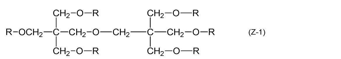

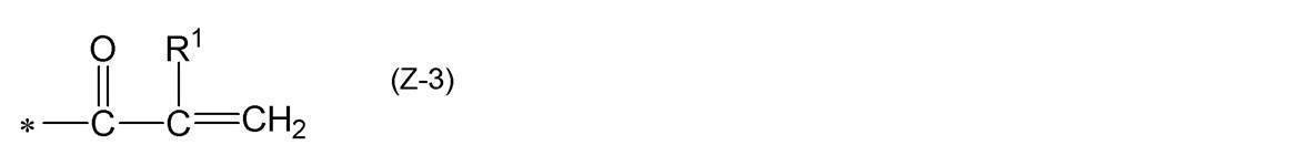

式(Z-4)中、(メタ)アクリロイル基の合計は3個又は4個であり、mは0~10の整数を表し、各mの合計は0~40の整数である。
式(Z-5)中、(メタ)アクリロイル基の合計は5個又は6個であり、nは0~10の整数を表し、各nの合計は0~60の整数である。
また、各mの合計は、2~40の整数が好ましく、2~16の整数がより好ましく、4~8の整数が更に好ましい。
式(Z-5)中、nは、0~6の整数が好ましく、0~4の整数がより好ましい。
また、各nの合計は、3~60の整数が好ましく、3~24の整数がより好ましく、6~12の整数が更に好ましい。
また、式(Z-4)又は式(Z-5)中の-((CH2)yCH2O)-又は-((CH2)yCH(CH3)O)-は、酸素原子側の末端がXに結合する形態が好ましい。
式(Z-4)又は式(Z-5)で表される化合物の中でも、ペンタエリスリトール誘導体及び/又はジペンタエリスリトール誘導体がより好ましい。
カルド骨格を含む上記重合性化合物としては、9,9-ビスアリールフルオレン骨格を含む上記重合性化合物が好ましい。
上記重合性化合物のエチレン性不飽和基の含有量(上記重合性化合物中のエチレン性不飽和基の数を、上記重合性化合物の分子量(g/mol)で除した値を意味する)は5.0mmol/g以上が好ましい。上限は特に制限されないが、一般に、20.0mmol/g以下である。
組成物は、樹脂を含んでいてもよい。
樹脂としては、(メタ)アクリル樹脂、エポキシ樹脂、エン・チオール樹脂、ポリカーボネート樹脂、ポリエーテル樹脂、ポリアリレート樹脂、ポリスルホン樹脂、ポリエーテルスルホン樹脂、ポリフェニレン樹脂、ポリアリーレンエーテルホスフィンオキシド樹脂、ポリイミド樹脂、ポリアミドイミド樹脂、ポリオレフィン樹脂、環状オレフィン樹脂、ポリエステル樹脂、スチレン樹脂、及び、フェノキシ樹脂等が挙げられる。
これらの樹脂から1種を単独で使用してもよく、2種以上を混合して使用してもよい。
また、樹脂の好適態様の一つとしては、酸基、塩基性基又はアミド基を有する樹脂が挙げられる。酸基、塩基性基又はアミド基を有する樹脂は、磁性体粒子を分散させる分散剤としての機能を発揮しやすい。
酸基としては、カルボキシ基、リン酸基、スルホ基、及び、フェノール性水酸基等が挙げられ、カルボキシ基が好ましい。
塩基性基としては、アミノ基(アンモニア、1級アミン又は2級アミンから水素原子を1つ除いた基)、及び、イミノ基が挙げられる。
中でも、樹脂は、カルボキシ基又はアミド基を有することが好ましい。
溶媒に対する樹脂の溶解度の上限値は、2000g/L以下が好ましく、1000g/L以下がより好ましい。
溶媒に対する樹脂の溶解度は、25℃における溶媒1Lに対する樹脂の溶解量(g)を意味する。
分散樹脂としては、グラフト鎖を含む繰り返し単位を有する樹脂(以下、「樹脂A」ともいう。)が挙げられる。ただし、樹脂Aは、分散剤としての機能を発揮させる以外の目的で使用できる。
グラフト鎖を含む繰り返し単位において、グラフト鎖が長くなると立体反発効果が高くなり磁性体粒子の分散性は向上する。一方、グラフト鎖が長すぎると磁性体粒子への吸着力が低下して、磁性体粒子の分散性は低下する傾向となる。このため、グラフト鎖は、水素原子を除いた原子数が40~10000であることが好ましく、水素原子を除いた原子数が50~2000であることがより好ましく、水素原子を除いた原子数が60~500であることが更に好ましい。
ここで、グラフト鎖とは、主鎖の根元(主鎖から枝分かれしている基において主鎖に結合する原子)から、主鎖から枝分かれしている基の末端までを示す。
グラフト鎖と溶媒との相互作用性を向上させ、それにより磁性体粒子の分散性を高めるために、グラフト鎖は、ポリエステル構造、ポリエーテル構造、及び、ポリ(メタ)アクリレート構造からなる群から選ばれる少なくとも1種を含むグラフト鎖であることが好ましく、ポリエステル構造及びポリエーテル構造の少なくともいずれかを含むグラフト鎖であることがより好ましい。
グラフト鎖を含むマクロモノマー(ポリマー構造を有し、主鎖に結合してグラフト鎖を構成するモノマー)としては、特に制限されないが、反応性二重結合性基を含むマクロモノマーを好適に使用できる。
ここで、ポリカプロラクトン構造とは、ε-カプロラクトンを開環した構造を繰り返し単位として含む構造をいう。ポリバレロラクトン構造とは、δ-バレロラクトンを開環した構造を繰り返し単位として含む構造をいう。
また、樹脂Aが後述する式(1)及び後述する式(2)におけるj及びkが4である繰り返し単位を含む場合、樹脂中に、上述したポリバレロラクトン構造を導入できる。
また、樹脂Aが後述する式(4)におけるX5が水素原子であり、R4がメチル基である繰り返し単位を含む場合、樹脂A中に、上述したポリアクリル酸メチル構造を導入できる。
また、樹脂Aが後述する式(4)におけるX5がメチル基であり、R4がメチル基である繰り返し単位を含む場合、樹脂A中に、上述したポリメタクリル酸メチル構造を導入できる。
式(1)~(4)において、X1、X2、X3、X4、及び、X5は、それぞれ独立に、水素原子又は1価の有機基を表す。X1、X2、X3、X4、及び、X5は、合成上の制約の点からは、それぞれ独立に、水素原子又は炭素数(炭素原子数)1~12のアルキル基が好ましく、それぞれ独立に、水素原子又はメチル基がより好ましく、メチル基が更に好ましい。
これらの中でも、Z1、Z2、Z3、及び、Z4で表される有機基としては、特に分散性向上の点から、立体反発効果を含む基が好ましく、それぞれ独立に、炭素数5~24のアルキル基又はアルコキシ基がより好ましく、その中でも、特にそれぞれ独立に炭素数5~24の分岐鎖状アルキル基、炭素数5~24の環状アルキル基、又は、炭素数5~24のアルコキシ基が更に好ましい。なお、アルコキシ基中に含まれるアルキル基は、直鎖状、分岐鎖状、及び、環状のいずれでもよい。
また、式(1)及び(2)において、j及びkは、それぞれ独立に、2~8の整数を表す。式(1)及び(2)におけるj及びkは、4~6の整数が好ましく、5がより好ましい。
また、式(1)及び(2)において、n及びmは、10以上の整数が好ましく、20以上の整数がより好ましい。また、樹脂Aが、ポリカプロラクトン構造、及びポリバレロラクトン構造を含む場合、ポリカプロラクトン構造の繰り返し数と、ポリバレロラクトンの繰返し数の和としては、10以上の整数が好ましく、20以上の整数がより好ましい。
式(4)中、R4は水素原子又は1価の有機基を表し、この1価の有機基の構造は特に制限されない。R4としては、水素原子、アルキル基、アリール基、又は、ヘテロアリール基が好ましく、水素原子又はアルキル基がより好ましい。R4がアルキル基である場合、アルキル基としては、炭素数1~20の直鎖状アルキル基、炭素数3~20の分岐鎖状アルキル基、又は、炭素数5~20の環状アルキル基が好ましく、炭素数1~20の直鎖状アルキル基がより好ましく、炭素数1~6の直鎖状アルキル基が更に好ましい。式(4)において、qが2~500のとき、グラフト鎖中に複数存在するX5及びR4は互いに同じであっても異なっていてもよい。
また、式(2)で表される繰り返し単位としては、下記式(2A)で表される繰り返し単位であることがより好ましい。
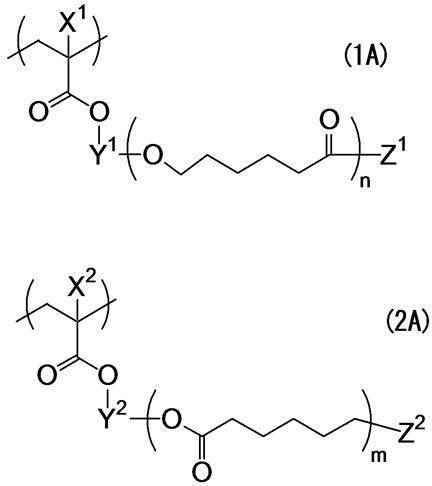


式(4A)及び式(4B)中の*としては、なかでも、隣接するアルキレンイミン鎖と結合する位置を表すことが好ましい。
アルキル基の炭素数としては、炭素数1~6が好ましく、炭素数1~3がより好ましい。
式(4A)中、RX1及びRX2としては、いずれも水素原子であることが好ましい。
式(4B)中、RX3及びRX4としては、いずれも水素原子であることが好ましい。
上記置換基としては、例えばアルキル基(例えば炭素数1~6のアルキル基)等の置換基が挙げられる。また、置換基として、ポリエステル鎖が結合してもよい。
上記ポリエステル鎖としては、下記式(5A)で表されるポリエステル鎖が挙げられる。

このようなポリエステル鎖としては、下記式(5B)で表されるポリエステル鎖が挙げられる。

RX6で表されるアルキル基は、XAで表されるアルキル基と同義である。また、RX7で表されるアルキレン基としては、XAで表されるアルキル基から水素原子を1つ除いた基が挙げられる。
pは、2以上の整数であり、その上限値としては、例えば10以下であり、5以下が好ましい。
上記アリール基は更に置換基を有していてもよく、置換基としては、アルキル基、ハロゲン原子、及び、シアノ基等が挙げられる。
また、樹脂Aは、グラフト鎖を含む繰り返し単位とは異なる(すなわち、グラフト鎖を含む繰り返し単位には相当しない)疎水性繰り返し単位を含んでいてもよい。ただし、本明細書において、疎水性繰り返し単位は、酸基(例えば、カルボン酸基、スルホン酸基、リン酸基、フェノール性水酸基等)を有さない繰り返し単位である。
A. J. Leo, Comprehensive Medicinal Chemistry, Vol.4, C. Hansch, P. G. Sammnens, J. B. Taylor and C. A. Ramsden, Eds., p.295, Pergamon Press, 1990 C. Hansch & A. J. Leo. SUbstituent Constants For Correlation Analysis in Chemistry and Biology. John Wiley & Sons. A.J. Leo. Calculating logPoct from structure. Chem. Rev., 93, 1281-1306, 1993.
logP=log(Coil/Cwater)
式中、Coilは油相中の化合物のモル濃度を、Cwaterは水相中の化合物のモル濃度を表す。
logPの値が0をはさんでプラスに大きくなると油溶性が増し、マイナスで絶対値が大きくなると水溶性が増し、有機化合物の水溶性と負の相関があり、有機化合物の親疎水性を見積るパラメータとして広く利用されている。
R1、R2、及び、R3は、水素原子又は炭素数が1~3のアルキル基であることが好ましく、水素原子又はメチル基であることがより好ましい。R2及びR3は、水素原子であることが更に好ましい。
Xは、酸素原子(-O-)又はイミノ基(-NH-)を表し、酸素原子が好ましい。
また、上記式(ii)で表される単量体として、R1が水素原子又はメチル基であって、Lがアルキレン基であって、Zが脂肪族基、複素環基、又は芳香族基である化合物が好ましい。また、上記式(iii)で表される単量体として、R4、R5、及びR6が水素原子又はメチル基であって、Zが脂肪族基、複素環基、又は芳香族基である化合物が好ましい。
樹脂Aは、磁性体粒子と相互作用を形成し得る官能基を有していてもよい。
樹脂Aは、磁性体粒子と相互作用を形成し得る官能基を含む繰り返し単位を更に含むことが好ましい。
磁性体粒子と相互作用を形成し得る官能基としては、例えば、酸基、塩基性基、配位性基、及び反応性を有する官能基等が挙げられる。
樹脂Aが、酸基、塩基性基、配位性基、又は、反応性を有する官能基を含む場合、それぞれ、酸基を含む繰り返し単位、塩基性基を含む繰り返し単位、配位性基を含む繰り返し単位、又は、反応性を有する官能基を有する繰り返し単位を含むことが好ましい。
すなわち、樹脂Aは、カルボン酸基、スルホン酸基、及び、リン酸基のうち少なくとも1種を含む繰り返し単位を更に含むことが好ましい。
樹脂Aが酸基を含む繰り返し単位を含む場合、その含有量は、質量換算で、樹脂Aの全質量に対して、5~80質量%が好ましく、10~60質量%がより好ましい。
樹脂Aが塩基性基を含む繰り返し単位を含む場合、その含有量は、質量換算で、樹脂Aの全質量に対して、0.01~50質量%が好ましく、0.01~30質量%がより好ましい。
樹脂Aが、配位性基を含む繰り返し単位、又は反応性を有する官能基を含む繰り返し単位を含む場合、これらの含有量は、質量換算で、樹脂Aの全質量に対して、10~80質量%が好ましく、20~60質量%がより好ましい。
式(iv)~(vi)中、R11、R12、及びR13としては、水素原子、又は炭素数が1~3のアルキル基が好ましく、水素原子又はメチル基がより好ましい。一般式(iv)中、R12及びR13としては、水素原子が更に好ましい。
また、式(v)中のYは、メチン基又は窒素原子を表す。
また、式(v)で表される単量体として、R11が水素原子又はメチル基であって、L1がアルキレン基であって、Z1がカルボン酸基であって、Yがメチン基である化合物が好ましい。
更に、式(vi)で表される単量体として、R14、R15、及びR16がそれぞれ独立に水素原子又はメチル基であって、Z1がカルボン酸基である化合物が好ましい。
樹脂Aは、エチレン性不飽和基を含んでいてもよい。
エチレン性不飽和基としては特に制限されないが、例えば、(メタ)アクリロイル基、ビニル基、及び、スチリル基等が挙げられ、(メタ)アクリロイル基が好ましい。
樹脂Aとしては、なかでも、側鎖にエチレン性不飽和基を含む繰り返し単位を含むことが好ましく、側鎖にエチレン性不飽和基を含み、且つ(メタ)アクリレートに由来する繰り返し単位(以下、「側鎖にエチレン性不飽和基を含む(メタ)アクリル系繰り返し単位」ともいう。)を含むことがより好ましい。
側鎖にエチレン性不飽和基を含む(メタ)アクリル系繰り返し単位は、例えば、カルボン酸基を含む(メタ)アクリル系繰り返し単位を含む樹脂A中の上記カルボン酸基に、グリシジル基又は脂環式エポキシ基を含むエチレン性不飽和化合物を付加反応させて得られる。このようにして導入されたエチレン性不飽和基(グリシジル基又は脂環式エポキシ基)を反応させれば、側鎖にエチレン性不飽和基を含む(メタ)アクリル系繰り返し単位を得ることができる。
更に、樹脂Aは、膜形成能等の諸性能を向上する目的で、本発明の効果を損なわない限りにおいて、グラフト鎖を含む繰り返し単位、疎水性繰り返し単位、及び、磁性体粒子と相互作用を形成し得る官能基を含む繰り返し単位とは異なる、種々の機能を有する他の繰り返し単位を更に有していてもよい。
このような、他の繰り返し単位としては、例えば、アクリロニトリル類、及び、メタクリロニトリル類等から選ばれるラジカル重合性化合物に由来の繰り返し単位が挙げられる。
樹脂Aは、これらの他の繰り返し単位を1種又は2種以上使用でき、その含有量は、質量換算で、樹脂Aの全質量に対して、0~80質量%が好ましく、10~60質量%がより好ましい。
樹脂Aの酸価としては特に制限されないが、例えば、0~400mgKOH/gが好ましく、10~350mgKOH/gがより好ましく、30~300mgKOH/gが更に好ましく、50~200mgKOH/gが特に好ましい。
樹脂Aの酸価が50mgKOH/g以上であれば、磁性体粒子の沈降安定性をより向上できる。
樹脂Aは、公知の方法に基づいて合成できる。
樹脂は、アルカリ可溶性樹脂を含んでいてもよい。本明細書において、アルカリ可溶性樹脂とは、アルカリ可溶性を促進する基(アルカリ可溶性基、例えばカルボン酸基等の酸基)を含む樹脂を意味し、既に説明した樹脂Aとは異なる樹脂を意味する。
不飽和カルボン酸としては特に制限されないが、(メタ)アクリル酸、クロトン酸、及び、ビニル酢酸等のモノカルボン酸類;イタコン酸、マレイン酸、及び、フマル酸等のジカルボン酸、又は、その酸無水物;並びに、フタル酸モノ(2-(メタ)アクリロイルオキシエチル)等の多価カルボン酸モノエステル類;等が挙げられる。
側鎖に含まれるエチレン性不飽和基としては、(メタ)アクリル酸基が好ましい。
側鎖にエチレン性不飽和基を含む繰り返し単位は、例えば、カルボン酸基を含む(メタ)アクリル系繰り返し単位のカルボン酸基に、グリシジル基又は脂環式エポキシ基を含むエチレン性不飽和化合物を付加反応させて得られる。
上記硬化性基としては、例えば、エチレン性不飽和基(例えば、(メタ)アクリロイル基、ビニル基、及び、スチリル基等)、及び、環状エーテル基(例えば、エポキシ基、オキセタニル基等)等が挙げられるが、これらに制限されない。
中でも、ラジカル反応で重合制御が可能な点で、硬化性基としては、エチレン性不飽和基が好ましく、(メタ)アクリロイル基がより好ましい。
硬化性基を含むアルカリ可溶性樹脂としては、硬化性基を側鎖に有するアルカリ可溶性樹脂等が好ましい。硬化性基を含むアルカリ可溶性樹脂としては、ダイヤナールNRシリーズ(三菱レイヨン社製)、Photomer6173(COOH含有 polyurethane acrylic oligomer.Diamond Shamrock Co.,Ltd.製)、ビスコートR-264、KSレジスト106(いずれも大阪有機化学工業社製)、サイクロマーPシリーズ(例えば、ACA230AA)、プラクセル CF200シリーズ(いずれもダイセル社製)、Ebecryl3800(ダイセル・オルネクス社製)、及び、アクリキュアRD-F8(日本触媒社製)等が挙げられる。
上記その他の付加重合性ビニルモノマーには、1種単独でも2種以上でもよい。
上記共重合体は、硬化性基を有することが好ましく、(メタ)アクリロイル基等のエチレン性不飽和基を含むことがより好ましい。
例えば、上記その他の付加重合性ビニルモノマーとして硬化性基を有するモノマーを使用して共重合体に硬化性基が導入されていてもよい。また、共重合体中の(メタ)アクリル酸に由来する単位及び/又は上記その他の付加重合性ビニルモノマーに由来する単位の1種以上の、一部又は全部に、硬化性基(好ましくは(メタ)アクリロイル基等のエチレン性不飽和基)が導入されていてもよい。
上記その他の付加重合性ビニルモノマーとしては、例えば、(メタ)アクリル酸メチル、スチレン系単量体(ヒドロキシスチレン等)、及び、エーテルダイマーが挙げられる。
上記エーテルダイマーは、例えば、下記一般式(ED1)で表される化合物、及び、下記一般式(ED2)で表される化合物が挙げられる。


組成物は、溶媒を含んでいてもよい。溶媒としては、水及び有機溶媒が挙げられ、有機溶媒が好ましい。
溶媒の沸点は、塗布性という点から、100~400℃が好ましく、150~300℃がより好ましく、170~250℃が更に好ましい。本明細書において、沸点とは、特に断りのない限り、標準沸点を意味する。
組成物は、重合開始剤を含んでいてもよい。
重合開始剤としては特に制限されず、公知の重合開始剤を使用できる。重合開始剤としては、例えば、光重合開始剤、及び、熱重合開始剤等が挙げられ、光重合開始剤が好ましい。なお、重合開始剤としては、いわゆるラジカル重合開始剤が好ましい。
組成物中における重合開始剤の含有量としては特に制限されないが、組成物の全固形分に対して、0.5~15質量%が好ましく、1.0~10質量%がより好ましく、1.5~8.0質量%が更に好ましい。


組成物は、上述した成分以外のその他の任意成分を更に含んでいてもよい。例えば、界面活性剤、重合禁止剤、酸化防止剤、増感剤、共増感剤、架橋剤(硬化剤)、硬化促進剤、熱硬化促進剤、可塑剤、希釈剤、感脂化剤、及び、ゴム成分等が挙げられ、更に、基板表面への密着促進剤及びその他の助剤類(例えば、消泡剤、難燃剤、レベリング剤、剥離促進剤、酸化防止剤、香料、表面張力調整剤、及び連鎖移動剤等)等の公知の添加剤を必要に応じて加えてもよい。
界面活性剤としては、フッ素系界面活性剤、ノニオン系界面活性剤、カチオン系界面活性剤、アニオン系界面活性剤、シリコーン系界面活性剤等の各種界面活性剤が挙げられる。界面活性剤については、国際公開第2015/166779号の段落0238~0245に記載された界面活性剤が挙げられ、この内容は本明細書に組み込まれる。
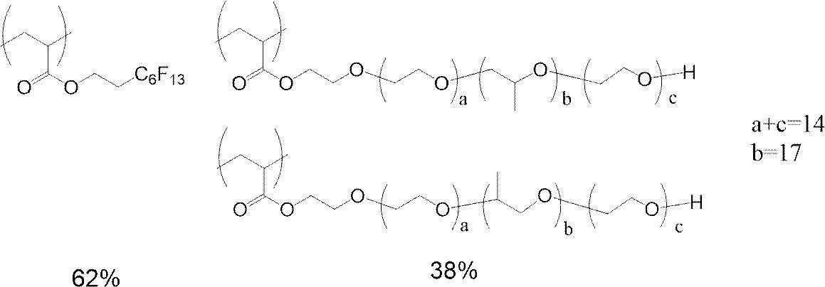

本発明の積層体の製造方法は、以下の工程1及び2を有する。
工程1:磁性体粒子及び重合性化合物を含む組成物を、アンテナが配置された基板上に塗布して、組成物層を形成する工程
工程2:組成物層に露光処理及び現像処理を施して、磁性体パターン部を形成する工程
以下、工程1及び2の手順について詳述する。
工程1では、磁性体粒子及び重合性化合物を含む組成物を、アンテナが配置された基板上に塗布して、組成物層を形成する。
使用される組成物及びアンテナが配置された基板は、上述した通りである。
塗布後、必要に応じて、乾燥処理を実施してもよい。乾燥(プリベーク)は、例えば、ホットプレート、オーブン等で50~140℃の温度で10~1800秒間で行える。
組成物層の膜厚としては、1~10000μmが好ましく、10~1000μmがより好ましく、15~800μmが更に好ましい。
工程2は、組成物層に露光処理及び現像処理を施して、磁性体パターン部を形成する工程である。
露光処理の方法は特に制限されないが、パターン状の開口部を有するフォトマスクを介して組成物層に光照射することが好ましい。フォトマスクのパターン状の開口部は、上述した所定の形状の磁性体パターン部が形成されるように配置される。
露光は、放射線の照射により行うことが好ましい。露光に際して使用できる放射線としては、g線、h線、及び、i線等の紫外線が好ましく、光源としては高圧水銀灯が好まれる。照射強度は5~1500mJ/cm2が好ましく、10~1000mJ/cm2がより好ましい。
ポストベークは、硬化を完全にするための現像後の加熱処理である。その加熱温度は、240℃以下が好ましく、220℃以下がより好ましい。下限は特にないが、効率的かつ効果的な処理を考慮すると、50℃以上が好ましく、100℃以上がより好ましい。
ポストベークは、ホットプレート、コンベクションオーブン(熱風循環式乾燥機)、及び、高周波加熱機等の加熱手段を用いて、連続式又はバッチ式で行える。
現像温度としては、例えば、20~30℃である。
現像時間は、例えば、20~90秒間である。残渣をよりよく除去するため、近年では120~180秒間実施する場合もある。更には、残渣除去性をより向上するため、現像液を60秒ごとに振り切り、更に新たに現像液を供給する工程を数回繰り返す場合もある。
アルカリ性化合物としては、例えば、水酸化ナトリウム、水酸化カリウム、炭酸ナトリウム,硅酸ナトリウム、メタ硅酸ナトリウム、アンモニア水、エチルアミン、ジエチルアミン、ジメチルエタノールアミン、テトラメチルアンモニウムヒドロキシド、テトラエチルアンモニウムヒドロキシド、テトラプロピルアンモニウムヒドロキシド、テトラブチルアンモニウムヒドロキシ、ベンジルトリメチルアンモニウムヒドロキシド、コリン、ピロール、ピペリジン、及び、1,8-ジアザビシクロ[5.4.0]-7-ウンデセン等が挙げられる(このうち、有機アルカリが好ましい。)。
なお、アルカリ現像液として用いた場合は、一般に現像後に水で洗浄処理が施される。
本実施例では、周波数が電磁波の60GHzに対する電磁波遮蔽による減衰を評価した。
基板上に、アンテナと、半導体素子を示すダミーパターンとを配置した。
アンテナは1辺が1.25mmの正方形とした。ダミーパターンは1辺が10mmの正方形の銅パッチで構成した。アンテナとダミーパターンとの距離を24mmとした。アンテナとダミーパターンとの間に磁性体パターン部を設けた。なお、磁性体パターン部を、幅1.25mm、間隔1.25mmを基準とした倍数の値とした。
[電磁波遮蔽による減衰]
送信アンテナとダミーパターンの位置に同じサイズの受信用パッチアンテナを配置し、カスケードプローブを介してAgilent E8361PNAネットワークアナライザを用い、周波数が電磁波の60GHzに対する電磁波遮蔽による減衰を、周波数60GHzの電磁波の減衰率(-dB)として計測した。
電磁波遮蔽による減衰(dB)は、以下に示す評価基準で評価した。
評価基準
A:-40dB以上
B:-40dB未満~-30dB以上
C:-30db未満~-20dB以上
D:-20dB未満
表1に示す、各種成分を混合して、組成物をそれぞれ調製した。
使用される各成分は以下の通りである。
(磁性体粒子)
・バリウムフェライト:以下の方法で合成した
液温35℃に保温した水400.0gを撹拌し、撹拌中の水に、塩化鉄(III)六水和物〔FeCl3・6H2O〕57.0g、塩化バリウム二水和物〔BaCl2・2H2O〕25.4g及び塩化アルミニウム六水和物〔AlCl3・6H2O〕10.2gを水216.0gに溶解して調製した原料水溶液と、濃度5mol/Lの水酸化ナトリウム水溶液181.3gに水113.0gを加えて調製した溶液と、をそれぞれ10mL/minの流速にて、添加のタイミングを同じにして全量添加し、第1の液を得た。
次いで、第1の液の液温を25℃とした後、この液温を保持した状態で、濃度1mol/Lの水酸化ナトリウム水溶液39.8gを添加し、第2の液を得た。得られた第2の液のpHは、10.5±0.5であった。pHは、卓上型pHメータ(堀場製作所社製F-71)を用いて測定した。
次いで、第2の液を15分間撹拌し、マグネトプランバイト型六方晶フェライトの前駆体となる沈殿物を含む液(前駆体含有液)を得た。
次いで、前駆体含有液に対し、遠心分離処理(回転数:2000rpm(revolutions per minute)、回転時間:10分間)を3回行い、得られた沈殿物を回収して水洗した。
次いで、回収した沈殿物を内部雰囲気温度95℃のオーブン内で12時間乾燥させて、前駆体の粉体を得た。
次いで、前駆体の粉体をマッフル炉の中に入れ、大気雰囲気下において、炉内の温度を1100℃に設定し、4時間焼成することにより、塊状の焼成体を得た。
次いで、得られた焼成体を、粉砕機として、カッターミル(大阪ケミカル社製ワンダークラッシャー WC-3)を使用し、この粉砕機の可変速度ダイアルを「5」(回転数:約10000~15000rpm)に設定して90秒間粉砕し、磁性粉末を得た。
-測定条件-
X線源:CuKα線
〔波長:1.54Å(0.154nm)、出力:40mA、45kV〕
スキャン範囲:20°<2θ<70°
スキャン間隔:0.05°
スキャンスピード:0.75°/min
上記X線回折分析の結果、得られた磁性粉体は、マグネトプランバイト型の結晶構造を有しており、マグネトプランバイト型以外の結晶構造を含まない単相のマグネトプランバイト型六方晶フェライトの粉体であることが確認された。
・X-1:以下構造式で表される樹脂。以下の式中の各繰り返し単位中の数値は、全繰り返し単位に対する含有量(質量%)を表す。

・X-2:以下構造式で表される樹脂。以下の式中の各繰り返し単位中の数値は、全繰り返し単位に対する含有量(質量%)を表す。

・B-1:以下構造式で表される樹脂。以下の式中の各繰り返し単位中の数値は、全繰り返し単位に対する含有量(質量%)を表す。

・B-3:以下構造式で表される樹脂。以下の式中の各繰り返し単位中の数値は、全繰り返し単位に対する含有量(質量%)を表す。

・KAYARAD DPHA(日本化薬社製、ジペンタエリスリトールヘキサアクリレートとジペンタエリスリトールペンタアクリレートの混合物)
・KAYARAD RP-1040(日本化薬社製、4官能アクリレート)
・NKエステル A-TMMT(新中村化学社製、多官能アクリレート)
・Irgacure OXE-01(BASF社製、オキシムエステル系開始剤)
・Irgacure OXE-03(BASF社製、オキシムエステル系開始剤)
・p-メトキシフェノール(三立ケミー社製)
・アデカスタブAO-80(ADEKA社製、下記構造の化合物)
・KF-6001(信越化学工業社製、両末端カルビノール変性ポリジメチルシロキサン、水酸基価62mgKOH/g)
・Polyfox PF6320(OMNOVA社製、フッ素系界面活性剤)
・PGMEA(プロピレングリコールモノメチルエーテルアセテート)
次に、図13に示すような磁性体パターン部が形成されるように、所定の開口部を有するマスクを介して、USHIO簡易露光装置にて、10mJ/cm2の条件で組成物層の露光処理を行った。
露光後、簡易現像装置(ミカサ社製)を用いて、23℃で60秒間のシャワー現像処理を行った。なお、現像液には、水酸化テトラメチルアンモニウム(TMAH)の含有量が0.3質量%である水溶液を用いた。
現像後、純水を用いたスピンシャワーによるリンス処理を行い、次いで、スピン乾燥した後、220℃のホットプレートを用いて5分間の加熱処理(ポストベーク)を行い、所定の形状の磁性体パターン部を形成した。
なお、比較例1においては磁性体粒子が使用されていなかった。また、比較例2においては重合性化合物が使用されていないため、現像処理の際に組成物層が全て除去されてしまい、磁性体パターン部が形成されなかった。
また、比較例3においては、上記露光処理を実施せずに、現像処理を実施した。そのため、現像処理の際に組成物層が全て除去されてしまい、磁性体パターン部が形成されなかった。
表1中、「磁性体粒子サイズ」は、磁性体粒子の平均一次粒子径を表す。
表1中、「膜厚」は、形成される磁性体パターン部の厚みを表す。
表1中、「L/S解像性」は、感光性磁性体組成物がUSHIO簡易露光装置で形成することができる最小パターンサイズを表す。
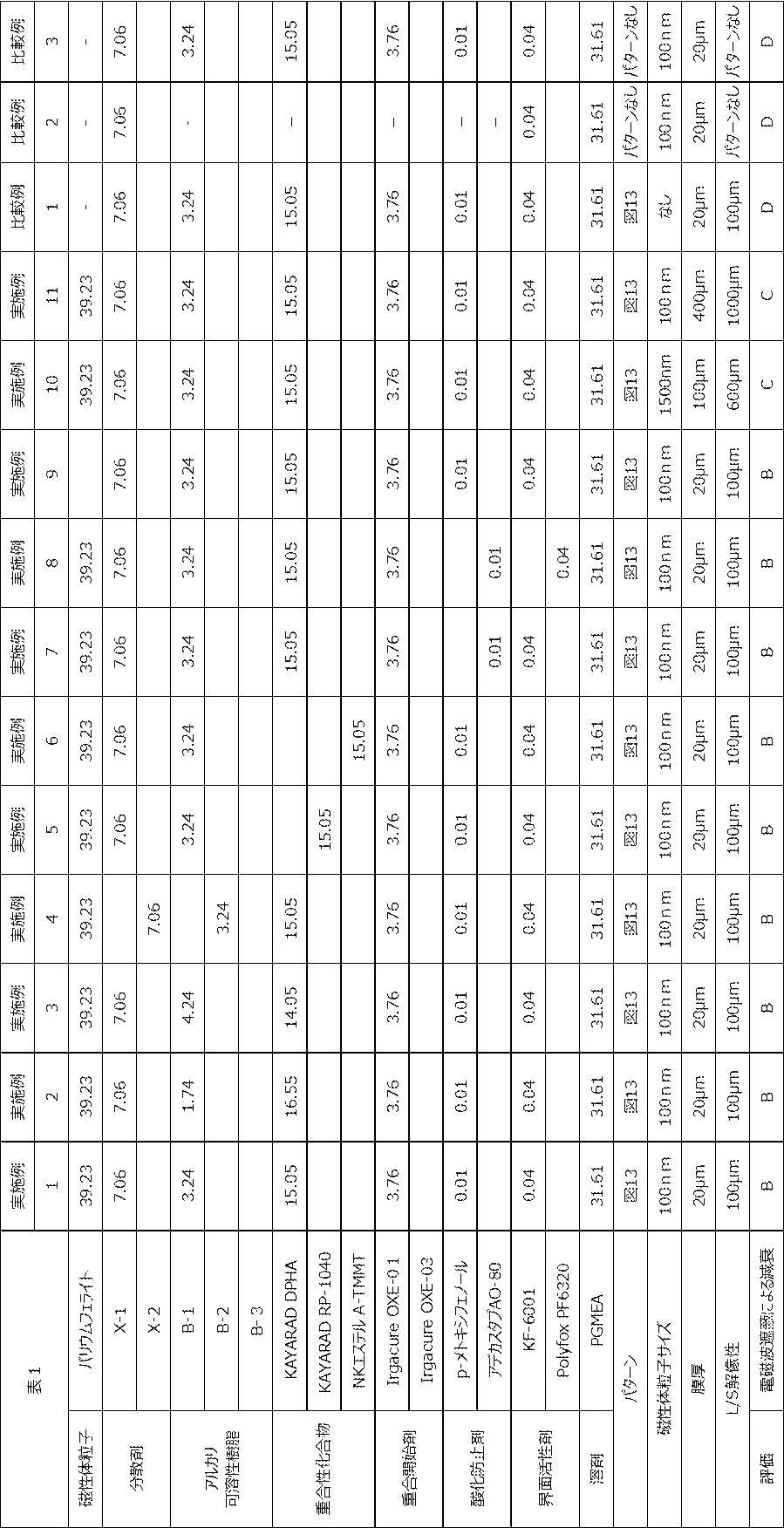
なかでも、実施例1と10との比較より、磁性体粒子が、Fe、Ni、及び、Coからなる群から選択される少なくとも1種の金属原子を含み、平均一次粒子径が20~1000nmである場合、より優れた効果が得られることが確認された。
また、実施例1と11との比較より、磁性体パターン部の厚みが300μm以下である場合、より優れた効果が 得られることが確認された。
パターンの種類、磁性体粒子の平均一次粒子径、磁性体パターン部の膜厚を後述する表に示すように変更した以外は、実施例1と同様の手順に従って、磁性体パターン部を有する積層体を製造した。
各実施例の結果を後述する表にまとめて示す。
実施例13は図19に示す磁性体パターン部とした。実施例13は、実施例12に比して、パターン部53の数が異なる以外は同じとした。
実施例14は図20に示す磁性体パターン部とした。実施例14では、距離Lcを10mmとした。パターン部53は、実施例12と同じとした。
実施例15は図21に示す磁性体パターン部とした。実施例15では、距離Lcを10mmとした。磁性体パターン部58の外直径を7mmとした。
実施例16は図22に示す磁性体パターン部とした。実施例16では、距離Lcを10mmとした。磁性体パターン部60の直径を7mmとした。
実施例17は図14に示す磁性体パターン部とした。第1パターン部50a、第2パターン部50b、及び第3パターン部50cの幅を1.25mmとし、間隔を1.25mmとした。
実施例18は図15に示す磁性体パターン部とした。第1パターン部50a、第2パターン部50b、及び第3パターン部50cの幅を1.25mmとし、間隔を2.5mmとした。
実施例19は図16に示す磁性体パターン部とした。第1パターン部50a、第2パターン部50b、及び第3パターン部50cの幅を1.25mmとし、間隔を3.75mmとした。
実施例21は図14に示す磁性体パターン部とし、L/Sを1/5とした。第1パターン部50a、第2パターン部50b、及び第3パターン部50cの幅を1.25mmとし、間隔を6.25mmとした。
実施例22は図14に示す磁性体パターン部とし、L/Sを1/6とした。第1パターン部50a、第2パターン部50b、及び第3パターン部50cの幅を1.25mmとし、間隔を7.5mmとした。
実施例23は図14に示す磁性体パターン部とし、L/Sを1/7とした。第1パターン部50a、第2パターン部50b、及び第3パターン部50cの幅を1.25mmとし、間隔を8.75mmとした。
実施例24は図4に示す磁性体パターン部とし、磁性体パターン部30の幅を1.25mmとし、磁性体パターン部30の内径を14mmとした。
実施例25は図5に示す磁性体パターン部とし、第1パターン部32aと第2パターン部32bとの幅を1.25mmとし、間隔を1.25mmとした。第1パターン部32aの内径を14mmとし、第2パターン部32bの最外径を21.5mmとした。
実施例27は図7に示す磁性体パターン部とし、第1パターン部36aと第2パターン部36bと第3パターン部36cと第4パターン部36dとの幅を1.25mmとし、間隔を1.25mmとした。第1パターン部36aの内径を14mmとし、第4パターン部36dの最外径を27.5mmとした。
実施例28は図8に示す磁性体パターン部とし、第1パターン部38aと第2パターン部38bと第3パターン部38cとの幅を1.25mmとし、間隔を1.25mmとした。第1パターン部38aの内部の高さを6.5mmとし、第3パターン部38cの最大高さを25.25mmとした。
実施例29は図9に示す磁性体パターン部とし、第1パターン部40aと第2パターン部40bと第3パターン部40cとの幅を1.25mmとし、間隔を1.25mmとした。第1パターン部40aの内側の辺の長さを7mmとし、第3パターン部40cの外側の辺の長さを19.5mmとした。
実施例31は図11に示す磁性体パターン部とし、第1パターン部44aと第2パターン部44bと第3パターン部44cとの幅を1.25mmとし、間隔を1.25mmとした。第1パターン部44aの内側の最大長さを10.67mmとし、第3パターン部44cの外側の最大長さを22.44mmとした。
実施例32は図12に示す磁性体パターン部とし、第1パターン部42aと第2パターン部42bと第3パターン部42cとの幅を1.25mmとし、間隔を1.25mmとした。第1パターン部42aの内側の最大長さを11.55mmとし、第3パターン部42cの外側の最大長さ、すなわち、外接円の直径を24.69mmとした。
実施例33は図24に示す磁性体パターン部とした。実施例33は、磁性体パターン部の幅を1.25mmとし、サブパターン部62dを7.5mmとし、サブパターン部62eを6.25mmとし、サブパターン部62fを3.75mmとた。パターン部62bを12.5mmとし、パターン部62cを13.75mmとした。
実施例35は図26に示す磁性体パターン部とした。実施例35は、磁性体パターン部の幅を1.25mmとし、長さLt及び長さLwを3.75mmとした。
実施例36は図27に示す磁性体パターン部とした。実施例36は、磁性体パターン部の幅を1.25mmとし、長さLt及び長さLwを3.75mmとした。
実施例37は図29に示す磁性体パターン部とした。実施例37は、パターン部70aの幅を1.25mmとし、長さLdを3.75mmとした。また、パターン部70aのアンテナ27から半導体素子28に向かう方向におけるピッチPwを3.13mmとし、上述の向かう方向と直交する方向におけるピッチPtを3.59mmとした。
実施例38は図30に示す磁性体パターン部とした。実施例38は、長さLt及び長さLwを3.75mmとした。
実施例39は図28に示す磁性体パターン部とした。実施例39は、開口部69aを一辺の長さが5mmの正方形とした。


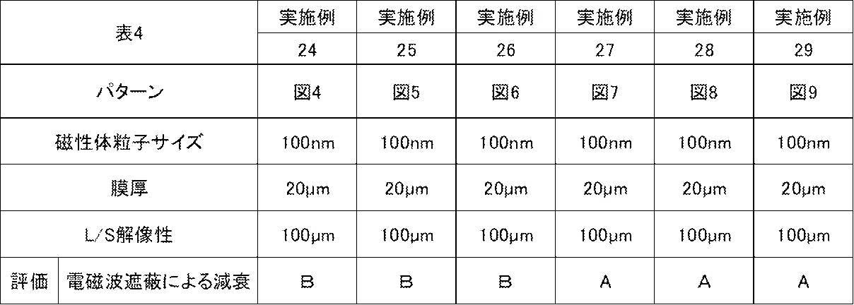


実施例12は、4つの円環状のパターン部をアンテナを囲んで配置した構成である。実施例13は、8つの円環状のパターン部をアンテナを囲んで配置した構成であり、アンテナの全周を囲んでいる。実施例13の方が、実施例12よりも電磁波が漏れる隙間が小さいため、電磁波を遮蔽する能力が高い。
実施例14~16は、アンテナと、ダミーパターンとの間に、1列状の磁性体パターン部を設けた構成であり、アンテナの全周を囲む構成ではない。しかしながら、実施例12よりも電磁波が漏れる隙間が小さく、電磁波を遮蔽する能力が高い。
実施例17~23は、いわゆるラインアンドスペースパターンである。L/Sの比率が大きいほど、電磁波の遮蔽能が計算上大きくなるが、実施例17~23では、差異が見られなかった。
実施例24はアンテナの全周囲を囲む1重円環状、実施例25はアンテナの全周囲を囲む2重円環状、実施例26はアンテナの全周囲を囲む3重円環状、実施例27はアンテナの全周囲を囲む4重円環状の磁性体パターン部である。実施例24~27から、実施例27の4重円環状の磁性体パターン部は、電磁波を遮蔽する能力が高い。
実施例28~32は、いずれも3重の多角形の磁性体パターン部を有する。実施例28~32のうち、三角形の実施例28、四角形の実施例29、六角形の実施例30は、3重円環状の実施例26よりも電磁波を遮蔽する能力が高い。八角形の実施例31、及び十角形の実施例32は、電磁波を遮蔽する能力が3重円環状の実施例26と同等であった。実施例31及び実施例32は、外形状が円に近くなり、磁性体のパターン部の形状による電磁波の吸収力が低下したことによるものと推測される。
実施例40~46は、3本のラインアンドスペースの組み合わせであるが、組み合わせた3本のラインアンドスペース同士は接続されていない。このため、電磁波のエネルギーが伝わって、共振することが抑制され、電磁波を遮蔽する能力が得られ、電磁波を遮蔽する能力が高い。
12 基板
12a 表面
14 アレイアンテナ
15、27 アンテナ
16 A/D回路
17 メモリ
18 ASIC
20 磁性体パターン部
22 組成物層
24 フォトマスク
25 マスク部
26 領域
28 半導体素子
30、32、34、36、37 磁性体パターン部
32a、34a、36a、37a、38a、40a 第1パターン部
32b、34b、36b、37b、38b、40b 第2パターン部
34c、36c、37c、38c、40c 第3パターン部
36d 第4パターン部 48d 第4パターン部
37d 切欠部
38、40、42、44 磁性体パターン部
42a、44a、46a、48a、50a 第1パターン部
42b、44b、46b、48b、50b 第2パターン部
42c、44c、46c、48c、50c 第3パターン部
46、48、50、52、54 磁性体パターン部
48e 第5パターン部
48f 第6パターン部
53 パターン部
53a 切欠部
53b 仮想的な正方形
56、58、60、62 磁性体パターン部
58a、60a、62a、62b、62c パターン部
62d、62e、62f サブパターン部
62g 構成パターン部
64、66、68、69、70、72 磁性体パターン部
66a 渦巻き型パターン部
66b、68a、68b、70a、72b パターン部
69a、70b、72a 開口部
Ld、Lf、Lg、Lh、Lt、Lw 長さ
Lv 露光光
Pt、Pw ピッチ
Claims (11)
- 磁性体粒子及び重合性化合物を含む組成物を、アンテナが配置された基板上に塗布して、組成物層を形成する工程と、
前記組成物層に露光処理及び現像処理を施して、磁性体パターン部を形成する工程とを有し、
前記磁性体パターン部は、前記アンテナの周囲のうち少なくとも一部に、前記アンテナと前記基板上において離間して配置される、積層体の製造方法。 - 前記基板上に、更に半導体素子が配置されており、
前記磁性体パターン部が、前記基板上において前記アンテナと前記半導体素子との間に配置される、請求項1に記載の積層体の製造方法。 - 前記磁性体パターン部が、前記アンテナの全周に存在する、請求項1又は2に記載の積層体の製造方法。
- 前記磁性体パターン部の幅は、前記アンテナから発信又は前記アンテナが受信する電磁波の波長の1/4の整数倍である、請求項1~3のいずれか1項に記載の積層体の製造方法。
- 前記磁性体パターン部は、前記アンテナから発信又は前記アンテナが受信する電磁波の波長の1/4の整数倍の間隔を有する、請求項1~4のいずれか1項に記載の積層体の製造方法。
- 前記磁性体パターン部は、前記アンテナから発信又は前記アンテナが受信する電磁波の波長の1/4の大きさの整数倍であるラインとスペースの組み合わせによって構成される、請求項1~3のいずれか1項に記載の積層体の製造方法。
- 前記磁性体パターン部の厚みは、300μm以下である、請求項1~6のいずれか1項に記載の積層体の製造方法。
- 前記磁性体粒子は、Fe、Ni、及び、Coからなる群から選択される少なくとも1種の金属原子を含む磁性体粒子であり、
前記磁性体粒子の平均一次粒子径が20~1000nmである、請求項1~7のいずれか1項に記載の積層体の製造方法。 - 請求項1~8のいずれか1項に記載の積層体の製造方法を含む、アンテナインパッケージの製造方法。
- 基板と、
前記基板上に配置されたアンテナと、
前記アンテナとは離間して、前記アンテナの周囲のうち少なくとも一部に配置された磁性体パターン部とを有する、積層体。 - 請求項10に記載の積層体中の磁性体パターン部の形成に用いられる組成物であって、
磁性体粒子及び重合性化合物を含む組成物。
Priority Applications (3)
| Application Number | Priority Date | Filing Date | Title |
|---|---|---|---|
| EP21872137.1A EP4220859A4 (en) | 2020-09-28 | 2021-09-06 | METHOD FOR MANUFACTURING LAMINATE, METHOD FOR MANUFACTURING ANTENNA HOUSING, LAMINATE AND COMPOSITION |
| JP2022551835A JPWO2022065006A1 (ja) | 2020-09-28 | 2021-09-06 | |
| US18/184,044 US20230216175A1 (en) | 2020-09-28 | 2023-03-15 | Method for producing laminate, method for producing antenna-in-package, laminate, and composition |
Applications Claiming Priority (2)
| Application Number | Priority Date | Filing Date | Title |
|---|---|---|---|
| JP2020-162310 | 2020-09-28 | ||
| JP2020162310 | 2020-09-28 |
Related Child Applications (1)
| Application Number | Title | Priority Date | Filing Date |
|---|---|---|---|
| US18/184,044 Continuation US20230216175A1 (en) | 2020-09-28 | 2023-03-15 | Method for producing laminate, method for producing antenna-in-package, laminate, and composition |
Publications (1)
| Publication Number | Publication Date |
|---|---|
| WO2022065006A1 true WO2022065006A1 (ja) | 2022-03-31 |
Family
ID=80845235
Family Applications (1)
| Application Number | Title | Priority Date | Filing Date |
|---|---|---|---|
| PCT/JP2021/032590 WO2022065006A1 (ja) | 2020-09-28 | 2021-09-06 | 積層体の製造方法、アンテナインパッケージの製造方法、積層体及び組成物 |
Country Status (5)
| Country | Link |
|---|---|
| US (1) | US20230216175A1 (ja) |
| EP (1) | EP4220859A4 (ja) |
| JP (1) | JPWO2022065006A1 (ja) |
| TW (1) | TW202212157A (ja) |
| WO (1) | WO2022065006A1 (ja) |
Citations (59)
| Publication number | Priority date | Publication date | Assignee | Title |
|---|---|---|---|---|
| JPS6288141A (ja) * | 1985-10-14 | 1987-04-22 | Fuji Photo Film Co Ltd | 磁気記録媒体製造方法 |
| JPH0336081B2 (ja) | 1983-03-23 | 1991-05-30 | Toyo Nainenki Kogyosha Kk | |
| JP2000066385A (ja) | 1998-08-18 | 2000-03-03 | Ciba Specialty Chem Holding Inc | 高感度で高レジスト厚さのi線ホトレジスト用スルホニルオキシム類 |
| JP2000080068A (ja) | 1998-06-26 | 2000-03-21 | Ciba Specialty Chem Holding Inc | 新規o―アシルオキシム光開始剤 |
| JP2001233842A (ja) | 1999-12-15 | 2001-08-28 | Ciba Specialty Chem Holding Inc | オキシムエステルの光開始剤 |
| JP2004534797A (ja) | 2001-06-11 | 2004-11-18 | チバ スペシャルティ ケミカルズ ホールディング インコーポレーテッド | 組み合わされた構造を有するオキシムエステルの光開始剤 |
| JP2006304080A (ja) * | 2005-04-22 | 2006-11-02 | Hitachi Metals Ltd | 磁性体で封止したアンテナを有する電子回路 |
| JP2008260927A (ja) | 2007-03-20 | 2008-10-30 | Toray Ind Inc | 黒色樹脂組成物、樹脂ブラックマトリクス、カラーフィルターおよび液晶表示装置 |
| JP2008292970A (ja) | 2006-09-27 | 2008-12-04 | Fujifilm Corp | 化合物及びその互変異性体、金属錯体化合物、感光性着色硬化性組成物、カラーフィルタ、及びその製造方法 |
| JP4223071B2 (ja) | 2006-12-27 | 2009-02-12 | 株式会社Adeka | オキシムエステル化合物及び該化合物を含有する光重合開始剤 |
| JP2010032698A (ja) | 2008-07-28 | 2010-02-12 | Fujifilm Corp | カラーフィルタ用着色硬化性組成物、カラーフィルタ、カラーフィルタの製造方法、及び液晶表示素子 |
| JP2010097210A (ja) | 2008-09-18 | 2010-04-30 | Toray Ind Inc | 感光性黒色樹脂組成物、樹脂ブラックマトリクス基板、カラーフィルター基板および液晶表示装置 |
| JP2010164965A (ja) | 2008-12-19 | 2010-07-29 | Mitsubishi Chemicals Corp | カラーフィルタ画素形成用組成物、カラーフィルタ、液晶表示装置及び有機elディスプレイ |
| JP2010168539A (ja) | 2008-12-26 | 2010-08-05 | Nippon Shokubai Co Ltd | α−アリルオキシメチルアクリル酸系重合体及びその製造方法 |
| JP2010527339A (ja) | 2007-05-11 | 2010-08-12 | ビーエーエスエフ ソシエタス・ヨーロピア | オキシムエステル光重合開始剤 |
| JP2010262028A (ja) | 2009-04-30 | 2010-11-18 | Nippon Steel Chem Co Ltd | ブラックマトリックス用感光性樹脂組成物 |
| JP2011132503A (ja) | 2009-11-25 | 2011-07-07 | Sumitomo Chemical Co Ltd | 樹脂組成物及び表示装置 |
| JP2011524436A (ja) | 2008-06-06 | 2011-09-01 | ビーエーエスエフ ソシエタス・ヨーロピア | 光開始剤混合物 |
| JP2012014052A (ja) | 2010-07-02 | 2012-01-19 | Fujifilm Corp | 着色感光性樹脂組成物、カラーフィルタ、カラーフィルタの製造方法、及び液晶表示装置 |
| JP2013029760A (ja) | 2011-07-29 | 2013-02-07 | Fujifilm Corp | 着色硬化性組成物、着色硬化膜、カラーフィルタ、パターン形成方法、カラーフィルタの製造方法、固体撮像素子及び画像表示装置 |
| JP2013114249A (ja) | 2011-12-01 | 2013-06-10 | Toppan Printing Co Ltd | 黒色感光性樹脂組成物およびカラーフィルタ |
| JP2013522445A (ja) | 2010-03-22 | 2013-06-13 | ヘンケル コーポレイション | マクロ光開始剤およびそれらの硬化性組成物 |
| WO2013083505A1 (en) | 2011-12-07 | 2013-06-13 | Basf Se | Oxime ester photoinitiators |
| JP2013164471A (ja) | 2012-02-09 | 2013-08-22 | Jsr Corp | 硬化性樹脂組成物、表示素子用硬化膜、表示素子用硬化膜の形成方法及び表示素子 |
| JP2013190459A (ja) | 2012-03-12 | 2013-09-26 | Tokyo Ohka Kogyo Co Ltd | 感光性樹脂組成物、カラーフィルタ、表示装置、光重合開始剤、及び化合物 |
| WO2013167515A1 (en) | 2012-05-09 | 2013-11-14 | Basf Se | Oxime ester photoinitiators |
| JP2014500852A (ja) | 2010-10-05 | 2014-01-16 | ビーエーエスエフ ソシエタス・ヨーロピア | ベンゾカルバゾール化合物のオキシムエステル誘導体ならびに前記誘導体の光重合性の組成物における光開始剤としての使用 |
| WO2014017669A1 (en) | 2012-07-27 | 2014-01-30 | Fujifilm Corporation | Near infrared absorptive liquid composition, near infrared cut filter using the same, method of manufacturing the same, and camera module and method of manufacturing the same |
| JP2014130173A (ja) | 2012-12-27 | 2014-07-10 | Fujifilm Corp | カラーフィルタ用組成物、赤外線透過フィルタ及びその製造方法、並びに赤外線センサー |
| JP2014137466A (ja) | 2013-01-16 | 2014-07-28 | Jsr Corp | 感放射線性着色組成物、着色硬化膜及び表示素子 |
| WO2015004565A1 (en) | 2013-07-08 | 2015-01-15 | Basf Se | Oxime ester photoinitiators |
| WO2015036910A1 (en) | 2013-09-10 | 2015-03-19 | Basf Se | Oxime ester photoinitiators |
| JP2015068893A (ja) | 2013-09-27 | 2015-04-13 | 東レ株式会社 | 樹脂ブラックマトリクス基板 |
| JP2015117327A (ja) | 2013-12-19 | 2015-06-25 | Dic株式会社 | 界面活性剤組成物、コーティング組成物及びレジスト組成物 |
| WO2015152153A1 (ja) | 2014-04-04 | 2015-10-08 | 株式会社Adeka | オキシムエステル化合物及び該化合物を含有する光重合開始剤 |
| WO2015166779A1 (ja) | 2014-05-01 | 2015-11-05 | 富士フイルム株式会社 | 着色組成物、膜、カラーフィルタ、パターン形成方法、カラーフィルタの製造方法、固体撮像素子および赤外線センサ |
| WO2016034963A1 (en) | 2014-09-04 | 2016-03-10 | Basf Se | Polycyclic photoinitiators |
| JP5923557B2 (ja) | 2013-06-24 | 2016-05-24 | 富士フイルム株式会社 | 磁気記録媒体および磁気記録媒体用塗料組成物 |
| KR20160109444A (ko) | 2015-03-11 | 2016-09-21 | 동우 화인켐 주식회사 | 청색 감광성 수지 조성물, 컬러필터 및 이를 포함하는 액정표시장치 |
| JP2016216602A (ja) | 2015-05-20 | 2016-12-22 | Dic株式会社 | フッ素系界面活性剤およびこれを含有する組成物 |
| WO2017033680A1 (ja) | 2015-08-26 | 2017-03-02 | パナソニックヘルスケアホールディングス株式会社 | 超低温フリーザ |
| WO2017051680A1 (ja) | 2015-09-25 | 2017-03-30 | 株式会社Adeka | オキシムエステル化合物及び該化合物を含有する重合開始剤 |
| WO2017110113A1 (ja) * | 2015-12-25 | 2017-06-29 | 株式会社トーキン | 電子装置及び電磁干渉抑制体の配置方法 |
| JP2017523465A (ja) | 2014-07-15 | 2017-08-17 | 常州強力電子新材料股▲ふん▼有限公司Cahngzhou Tronly New Electronic Materials Co.,Ltd. | オキシムエステル類光開始剤含有感光性組成物及びその使用 |
| JP2017151342A (ja) | 2016-02-26 | 2017-08-31 | 東洋インキScホールディングス株式会社 | 感光性着色組成物およびカラーフィルタ |
| JP2017167399A (ja) | 2016-03-17 | 2017-09-21 | 株式会社Dnpファインケミカル | カラーフィルタ用感光性着色樹脂組成物、カラーフィルタ、表示装置 |
| WO2017164127A1 (ja) | 2016-03-25 | 2017-09-28 | 東レ株式会社 | 着色樹脂組成物、カラーフィルタ基板、および液晶表示装置 |
| JP2017198865A (ja) | 2016-04-27 | 2017-11-02 | 東京応化工業株式会社 | 感光性組成物 |
| JP6301489B2 (ja) | 2014-03-18 | 2018-03-28 | 常州強力電子新材料股▲ふん▼有限公司Cahngzhou Tronly New Electronic Materials Co.,Ltd. | ニトロ基含有ビスオキシムエステル系光重合開始剤及びその合成製造方法と応用 |
| WO2018110179A1 (ja) | 2016-12-13 | 2018-06-21 | 日油株式会社 | ペルオキシシンナメート誘導体、該化合物を含有する重合性組成物 |
| WO2018221177A1 (ja) | 2017-06-01 | 2018-12-06 | 日油株式会社 | トリアジンペルオキシド誘導体、該化合物を含有する重合性組成物 |
| JP2019044030A (ja) | 2017-08-31 | 2019-03-22 | 学校法人東京理科大学 | ペルオキシエステル基を有するチオキサントン誘導体を含有する重合性組成物およびその硬化物、当該硬化物の製造方法 |
| JP2019043864A (ja) | 2017-08-31 | 2019-03-22 | 学校法人東京理科大学 | ペルオキシエステル基を有するベンゾフェノン誘導体、該化合物を含有する重合性組成物およびその硬化物、当該硬化物の製造方法 |
| JP2019057730A (ja) | 2018-12-12 | 2019-04-11 | 日東電工株式会社 | 電磁波吸収体 |
| WO2019088055A1 (ja) | 2017-10-30 | 2019-05-09 | 株式会社Adeka | 化合物、組成物、硬化物及び硬化物の製造方法 |
| JP2019167313A (ja) | 2018-03-26 | 2019-10-03 | 日油株式会社 | ペルオキシシンナメート誘導体、該化合物を含有する重合性組成物およびその硬化物、並びに当該硬化物の製造方法 |
| JP2020008634A (ja) | 2018-07-04 | 2020-01-16 | 三菱ケミカル株式会社 | 感光性樹脂組成物、隔壁、有機電界発光素子、画像表示装置及び照明 |
| JP2020055992A (ja) | 2018-07-17 | 2020-04-09 | 奇▲たい▼科技股▲ふん▼有限公司 | 液体光開始化合物とその用途 |
| WO2020084854A1 (ja) | 2018-10-24 | 2020-04-30 | 三菱マテリアル電子化成株式会社 | 含フッ素イミド塩化合物及び界面活性剤 |
Family Cites Families (3)
| Publication number | Priority date | Publication date | Assignee | Title |
|---|---|---|---|---|
| WO2007083430A1 (ja) * | 2006-01-20 | 2007-07-26 | Matsushita Electric Industrial Co., Ltd. | アンテナ内蔵モジュールとカード型情報装置およびそれらの製造方法 |
| US9386688B2 (en) * | 2010-11-12 | 2016-07-05 | Freescale Semiconductor, Inc. | Integrated antenna package |
| WO2020179349A1 (ja) * | 2019-03-01 | 2020-09-10 | リンテック株式会社 | 電磁波吸収フィルム、電磁波吸収シート |
-
2021
- 2021-09-06 WO PCT/JP2021/032590 patent/WO2022065006A1/ja active Application Filing
- 2021-09-06 JP JP2022551835A patent/JPWO2022065006A1/ja active Pending
- 2021-09-06 EP EP21872137.1A patent/EP4220859A4/en active Pending
- 2021-09-14 TW TW110134272A patent/TW202212157A/zh unknown
-
2023
- 2023-03-15 US US18/184,044 patent/US20230216175A1/en active Pending
Patent Citations (65)
| Publication number | Priority date | Publication date | Assignee | Title |
|---|---|---|---|---|
| JPH0336081B2 (ja) | 1983-03-23 | 1991-05-30 | Toyo Nainenki Kogyosha Kk | |
| JPS6288141A (ja) * | 1985-10-14 | 1987-04-22 | Fuji Photo Film Co Ltd | 磁気記録媒体製造方法 |
| JP2000080068A (ja) | 1998-06-26 | 2000-03-21 | Ciba Specialty Chem Holding Inc | 新規o―アシルオキシム光開始剤 |
| JP2000066385A (ja) | 1998-08-18 | 2000-03-03 | Ciba Specialty Chem Holding Inc | 高感度で高レジスト厚さのi線ホトレジスト用スルホニルオキシム類 |
| JP2001233842A (ja) | 1999-12-15 | 2001-08-28 | Ciba Specialty Chem Holding Inc | オキシムエステルの光開始剤 |
| JP2004534797A (ja) | 2001-06-11 | 2004-11-18 | チバ スペシャルティ ケミカルズ ホールディング インコーポレーテッド | 組み合わされた構造を有するオキシムエステルの光開始剤 |
| JP2006342166A (ja) | 2001-06-11 | 2006-12-21 | Ciba Specialty Chem Holding Inc | 組み合わされた構造を有するオキシムエステルの光開始剤 |
| JP2006304080A (ja) * | 2005-04-22 | 2006-11-02 | Hitachi Metals Ltd | 磁性体で封止したアンテナを有する電子回路 |
| JP2008292970A (ja) | 2006-09-27 | 2008-12-04 | Fujifilm Corp | 化合物及びその互変異性体、金属錯体化合物、感光性着色硬化性組成物、カラーフィルタ、及びその製造方法 |
| JP4223071B2 (ja) | 2006-12-27 | 2009-02-12 | 株式会社Adeka | オキシムエステル化合物及び該化合物を含有する光重合開始剤 |
| JP2008260927A (ja) | 2007-03-20 | 2008-10-30 | Toray Ind Inc | 黒色樹脂組成物、樹脂ブラックマトリクス、カラーフィルターおよび液晶表示装置 |
| JP2010527339A (ja) | 2007-05-11 | 2010-08-12 | ビーエーエスエフ ソシエタス・ヨーロピア | オキシムエステル光重合開始剤 |
| JP2011524436A (ja) | 2008-06-06 | 2011-09-01 | ビーエーエスエフ ソシエタス・ヨーロピア | 光開始剤混合物 |
| JP2010032698A (ja) | 2008-07-28 | 2010-02-12 | Fujifilm Corp | カラーフィルタ用着色硬化性組成物、カラーフィルタ、カラーフィルタの製造方法、及び液晶表示素子 |
| JP2010097210A (ja) | 2008-09-18 | 2010-04-30 | Toray Ind Inc | 感光性黒色樹脂組成物、樹脂ブラックマトリクス基板、カラーフィルター基板および液晶表示装置 |
| JP2010164965A (ja) | 2008-12-19 | 2010-07-29 | Mitsubishi Chemicals Corp | カラーフィルタ画素形成用組成物、カラーフィルタ、液晶表示装置及び有機elディスプレイ |
| JP2010168539A (ja) | 2008-12-26 | 2010-08-05 | Nippon Shokubai Co Ltd | α−アリルオキシメチルアクリル酸系重合体及びその製造方法 |
| JP2010262028A (ja) | 2009-04-30 | 2010-11-18 | Nippon Steel Chem Co Ltd | ブラックマトリックス用感光性樹脂組成物 |
| JP2011132503A (ja) | 2009-11-25 | 2011-07-07 | Sumitomo Chemical Co Ltd | 樹脂組成物及び表示装置 |
| JP2013522445A (ja) | 2010-03-22 | 2013-06-13 | ヘンケル コーポレイション | マクロ光開始剤およびそれらの硬化性組成物 |
| JP2012014052A (ja) | 2010-07-02 | 2012-01-19 | Fujifilm Corp | 着色感光性樹脂組成物、カラーフィルタ、カラーフィルタの製造方法、及び液晶表示装置 |
| JP2014500852A (ja) | 2010-10-05 | 2014-01-16 | ビーエーエスエフ ソシエタス・ヨーロピア | ベンゾカルバゾール化合物のオキシムエステル誘導体ならびに前記誘導体の光重合性の組成物における光開始剤としての使用 |
| JP2013029760A (ja) | 2011-07-29 | 2013-02-07 | Fujifilm Corp | 着色硬化性組成物、着色硬化膜、カラーフィルタ、パターン形成方法、カラーフィルタの製造方法、固体撮像素子及び画像表示装置 |
| JP2013114249A (ja) | 2011-12-01 | 2013-06-10 | Toppan Printing Co Ltd | 黒色感光性樹脂組成物およびカラーフィルタ |
| WO2013083505A1 (en) | 2011-12-07 | 2013-06-13 | Basf Se | Oxime ester photoinitiators |
| JP2013164471A (ja) | 2012-02-09 | 2013-08-22 | Jsr Corp | 硬化性樹脂組成物、表示素子用硬化膜、表示素子用硬化膜の形成方法及び表示素子 |
| JP2013190459A (ja) | 2012-03-12 | 2013-09-26 | Tokyo Ohka Kogyo Co Ltd | 感光性樹脂組成物、カラーフィルタ、表示装置、光重合開始剤、及び化合物 |
| WO2013167515A1 (en) | 2012-05-09 | 2013-11-14 | Basf Se | Oxime ester photoinitiators |
| JP2017019766A (ja) | 2012-05-09 | 2017-01-26 | ビーエーエスエフ ソシエタス・ヨーロピアBasf Se | オキシムエステル光開始剤 |
| WO2014017669A1 (en) | 2012-07-27 | 2014-01-30 | Fujifilm Corporation | Near infrared absorptive liquid composition, near infrared cut filter using the same, method of manufacturing the same, and camera module and method of manufacturing the same |
| JP2014041318A (ja) | 2012-07-27 | 2014-03-06 | Fujifilm Corp | 近赤外線吸収性組成物、これを用いた近赤外線カットフィルタ及びその製造方法、並びに、カメラモジュール及びその製造方法 |
| JP2014130173A (ja) | 2012-12-27 | 2014-07-10 | Fujifilm Corp | カラーフィルタ用組成物、赤外線透過フィルタ及びその製造方法、並びに赤外線センサー |
| JP2014137466A (ja) | 2013-01-16 | 2014-07-28 | Jsr Corp | 感放射線性着色組成物、着色硬化膜及び表示素子 |
| JP6065596B2 (ja) | 2013-01-16 | 2017-01-25 | Jsr株式会社 | 感放射線性着色組成物、着色硬化膜及び表示素子 |
| JP5923557B2 (ja) | 2013-06-24 | 2016-05-24 | 富士フイルム株式会社 | 磁気記録媒体および磁気記録媒体用塗料組成物 |
| WO2015004565A1 (en) | 2013-07-08 | 2015-01-15 | Basf Se | Oxime ester photoinitiators |
| JP6469669B2 (ja) | 2013-07-08 | 2019-02-13 | ビーエーエスエフ ソシエタス・ヨーロピアBasf Se | オキシムエステル光開始剤 |
| JP2016532675A (ja) | 2013-07-08 | 2016-10-20 | ビーエーエスエフ ソシエタス・ヨーロピアBasf Se | オキシムエステル光開始剤 |
| WO2015036910A1 (en) | 2013-09-10 | 2015-03-19 | Basf Se | Oxime ester photoinitiators |
| JP2015068893A (ja) | 2013-09-27 | 2015-04-13 | 東レ株式会社 | 樹脂ブラックマトリクス基板 |
| JP2015117327A (ja) | 2013-12-19 | 2015-06-25 | Dic株式会社 | 界面活性剤組成物、コーティング組成物及びレジスト組成物 |
| JP6301489B2 (ja) | 2014-03-18 | 2018-03-28 | 常州強力電子新材料股▲ふん▼有限公司Cahngzhou Tronly New Electronic Materials Co.,Ltd. | ニトロ基含有ビスオキシムエステル系光重合開始剤及びその合成製造方法と応用 |
| WO2015152153A1 (ja) | 2014-04-04 | 2015-10-08 | 株式会社Adeka | オキシムエステル化合物及び該化合物を含有する光重合開始剤 |
| WO2015166779A1 (ja) | 2014-05-01 | 2015-11-05 | 富士フイルム株式会社 | 着色組成物、膜、カラーフィルタ、パターン形成方法、カラーフィルタの製造方法、固体撮像素子および赤外線センサ |
| JP2017523465A (ja) | 2014-07-15 | 2017-08-17 | 常州強力電子新材料股▲ふん▼有限公司Cahngzhou Tronly New Electronic Materials Co.,Ltd. | オキシムエステル類光開始剤含有感光性組成物及びその使用 |
| WO2016034963A1 (en) | 2014-09-04 | 2016-03-10 | Basf Se | Polycyclic photoinitiators |
| KR20160109444A (ko) | 2015-03-11 | 2016-09-21 | 동우 화인켐 주식회사 | 청색 감광성 수지 조성물, 컬러필터 및 이를 포함하는 액정표시장치 |
| JP2016216602A (ja) | 2015-05-20 | 2016-12-22 | Dic株式会社 | フッ素系界面活性剤およびこれを含有する組成物 |
| WO2017033680A1 (ja) | 2015-08-26 | 2017-03-02 | パナソニックヘルスケアホールディングス株式会社 | 超低温フリーザ |
| WO2017051680A1 (ja) | 2015-09-25 | 2017-03-30 | 株式会社Adeka | オキシムエステル化合物及び該化合物を含有する重合開始剤 |
| WO2017110113A1 (ja) * | 2015-12-25 | 2017-06-29 | 株式会社トーキン | 電子装置及び電磁干渉抑制体の配置方法 |
| JP2017151342A (ja) | 2016-02-26 | 2017-08-31 | 東洋インキScホールディングス株式会社 | 感光性着色組成物およびカラーフィルタ |
| JP2017167399A (ja) | 2016-03-17 | 2017-09-21 | 株式会社Dnpファインケミカル | カラーフィルタ用感光性着色樹脂組成物、カラーフィルタ、表示装置 |
| WO2017164127A1 (ja) | 2016-03-25 | 2017-09-28 | 東レ株式会社 | 着色樹脂組成物、カラーフィルタ基板、および液晶表示装置 |
| JP2017198865A (ja) | 2016-04-27 | 2017-11-02 | 東京応化工業株式会社 | 感光性組成物 |
| WO2018110179A1 (ja) | 2016-12-13 | 2018-06-21 | 日油株式会社 | ペルオキシシンナメート誘導体、該化合物を含有する重合性組成物 |
| WO2018221177A1 (ja) | 2017-06-01 | 2018-12-06 | 日油株式会社 | トリアジンペルオキシド誘導体、該化合物を含有する重合性組成物 |
| JP2019044030A (ja) | 2017-08-31 | 2019-03-22 | 学校法人東京理科大学 | ペルオキシエステル基を有するチオキサントン誘導体を含有する重合性組成物およびその硬化物、当該硬化物の製造方法 |
| JP2019043864A (ja) | 2017-08-31 | 2019-03-22 | 学校法人東京理科大学 | ペルオキシエステル基を有するベンゾフェノン誘導体、該化合物を含有する重合性組成物およびその硬化物、当該硬化物の製造方法 |
| WO2019088055A1 (ja) | 2017-10-30 | 2019-05-09 | 株式会社Adeka | 化合物、組成物、硬化物及び硬化物の製造方法 |
| JP2019167313A (ja) | 2018-03-26 | 2019-10-03 | 日油株式会社 | ペルオキシシンナメート誘導体、該化合物を含有する重合性組成物およびその硬化物、並びに当該硬化物の製造方法 |
| JP2020008634A (ja) | 2018-07-04 | 2020-01-16 | 三菱ケミカル株式会社 | 感光性樹脂組成物、隔壁、有機電界発光素子、画像表示装置及び照明 |
| JP2020055992A (ja) | 2018-07-17 | 2020-04-09 | 奇▲たい▼科技股▲ふん▼有限公司 | 液体光開始化合物とその用途 |
| WO2020084854A1 (ja) | 2018-10-24 | 2020-04-30 | 三菱マテリアル電子化成株式会社 | 含フッ素イミド塩化合物及び界面活性剤 |
| JP2019057730A (ja) | 2018-12-12 | 2019-04-11 | 日東電工株式会社 | 電磁波吸収体 |
Non-Patent Citations (5)
| Title |
|---|
| A. J. LEO: "Calculating log Poct from structure", CHEM. REV., vol. 93, 1993, pages 1281 - 1306 |
| A. J. LEO: "Comprehensive Medicinal Chemistry", vol. 4, 1990, PERGAMON PRESS, pages: 295 |
| JOURNAL OF PHOTOPOLYMER SCIENCE AND TECHNOLOGY, 1995, pages 202 - 232 |
| MATERIAL STAGE, vol. 19, no. 3, 2019, pages 37 - 60 |
| See also references of EP4220859A4 |
Also Published As
| Publication number | Publication date |
|---|---|
| EP4220859A4 (en) | 2024-03-27 |
| EP4220859A1 (en) | 2023-08-02 |
| TW202212157A (zh) | 2022-04-01 |
| JPWO2022065006A1 (ja) | 2022-03-31 |
| US20230216175A1 (en) | 2023-07-06 |
Similar Documents
| Publication | Publication Date | Title |
|---|---|---|
| KR102029639B1 (ko) | 전계 효과 트랜지스터의 제조 방법 및 무선 통신 장치의 제조 방법 | |
| WO2021117395A1 (ja) | 磁性粒子含有膜、積層体及び電子部品 | |
| JP6694513B2 (ja) | 遮光性組成物、遮光膜、固体撮像素子、カラーフィルタ、及び、液晶表示装置 | |
| JP7018126B2 (ja) | 導熱層、感光層、感光性組成物、導熱層の製造方法、並びに、積層体および半導体デバイス | |
| KR102453516B1 (ko) | 경화막의 제조 방법, 고체 촬상 소자의 제조 방법 | |
| JPWO2018180477A1 (ja) | 着色膜及びその製造方法、固体撮像素子 | |
| US20220375668A1 (en) | Magnetic particle-containing composition, magnetic particle-containing film, and electronic component | |
| WO2018061644A1 (ja) | 金属窒化物含有粒子、分散組成物、硬化性組成物、硬化膜、及びそれらの製造方法、並びにカラーフィルタ、固体撮像素子、固体撮像装置、赤外線センサ | |
| WO2022065006A1 (ja) | 積層体の製造方法、アンテナインパッケージの製造方法、積層体及び組成物 | |
| KR20220146572A (ko) | 착색 감광성 조성물, 경화물, 컬러 필터, 고체 촬상 소자, 및, 화상 표시 장치 | |
| JPWO2018173692A1 (ja) | 硬化性組成物、硬化膜、遮光膜、固体撮像素子、固体撮像装置、及び、硬化膜の製造方法 | |
| KR102603923B1 (ko) | 감광성 수지 조성물, 경화막, 인덕터, 안테나 | |
| US20240032186A1 (en) | Structure, method for manufacturing structure, and composition | |
| KR20230146036A (ko) | 조성물, 자성 입자 함유 경화물, 자성 입자 도입 기판, 전자 재료 | |
| JP5689691B2 (ja) | チタンブラック分散物、感光性樹脂組成物、遮光膜及びその製造方法、並びに固体撮像素子 | |
| TW202309144A (zh) | 含三嗪環聚合物,及圖型形成用組成物 | |
| JP7083887B2 (ja) | 硬化性組成物、硬化膜、光学素子、固体撮像素子、カラーフィルタ | |
| WO2024048110A1 (ja) | 構造体、及び構造体の製造方法 | |
| KR20230030648A (ko) | 착색 조성물, 경화물, 컬러 필터, 고체 촬상 소자, 화상 표시 장치, 및, 수지 및 그 제조 방법 | |
| TW202130601A (zh) | 組成物、膜、硬化膜、硬化膜的製造方法、電子元件 | |
| WO2022059706A1 (ja) | 組成物、磁性粒子含有膜、及び、電子部品 | |
| TW202208544A (zh) | 組成物、含有磁性粒子之膜及電子零件 | |
| CN116964697A (zh) | 组合物、含磁性粒子的固化物、磁性粒子导入基板、电子材料 | |
| KR20220137949A (ko) | 감광성 조성물, 경화막, 컬러 필터, 차광막, 광학 소자, 고체 촬상 소자, 적외선 센서, 헤드라이트 유닛 |
Legal Events
| Date | Code | Title | Description |
|---|---|---|---|
| 121 | Ep: the epo has been informed by wipo that ep was designated in this application |
Ref document number: 21872137 Country of ref document: EP Kind code of ref document: A1 |
|
| ENP | Entry into the national phase |
Ref document number: 2022551835 Country of ref document: JP Kind code of ref document: A |
|
| WWE | Wipo information: entry into national phase |
Ref document number: 2021872137 Country of ref document: EP |
|
| NENP | Non-entry into the national phase |
Ref country code: DE |
|
| ENP | Entry into the national phase |
Ref document number: 2021872137 Country of ref document: EP Effective date: 20230428 |