WO2017154432A1 - 多層積層板及びこれを用いた多層プリント配線板の製造方法 - Google Patents
多層積層板及びこれを用いた多層プリント配線板の製造方法 Download PDFInfo
- Publication number
- WO2017154432A1 WO2017154432A1 PCT/JP2017/003966 JP2017003966W WO2017154432A1 WO 2017154432 A1 WO2017154432 A1 WO 2017154432A1 JP 2017003966 W JP2017003966 W JP 2017003966W WO 2017154432 A1 WO2017154432 A1 WO 2017154432A1
- Authority
- WO
- WIPO (PCT)
- Prior art keywords
- layer
- dielectric layer
- dielectric
- conductive layer
- multilayer
- Prior art date
- Legal status (The legal status is an assumption and is not a legal conclusion. Google has not performed a legal analysis and makes no representation as to the accuracy of the status listed.)
- Ceased
Links
Images


Classifications
-
- H—ELECTRICITY
- H05—ELECTRIC TECHNIQUES NOT OTHERWISE PROVIDED FOR
- H05K—PRINTED CIRCUITS; CASINGS OR CONSTRUCTIONAL DETAILS OF ELECTRIC APPARATUS; MANUFACTURE OF ASSEMBLAGES OF ELECTRICAL COMPONENTS
- H05K3/00—Apparatus or processes for manufacturing printed circuits
- H05K3/46—Manufacturing multilayer circuits
- H05K3/4611—Manufacturing multilayer circuits by laminating two or more circuit boards
- H05K3/4626—Manufacturing multilayer circuits by laminating two or more circuit boards characterised by the insulating layers or materials
- H05K3/4629—Manufacturing multilayer circuits by laminating two or more circuit boards characterised by the insulating layers or materials laminating inorganic sheets comprising printed circuits, e.g. green ceramic sheets
-
- B—PERFORMING OPERATIONS; TRANSPORTING
- B32—LAYERED PRODUCTS
- B32B—LAYERED PRODUCTS, i.e. PRODUCTS BUILT-UP OF STRATA OF FLAT OR NON-FLAT, e.g. CELLULAR OR HONEYCOMB, FORM
- B32B7/00—Layered products characterised by the relation between layers; Layered products characterised by the relative orientation of features between layers, or by the relative values of a measurable parameter between layers, i.e. products comprising layers having different physical, chemical or physicochemical properties; Layered products characterised by the interconnection of layers
- B32B7/02—Physical, chemical or physicochemical properties
- B32B7/025—Electric or magnetic properties
-
- B—PERFORMING OPERATIONS; TRANSPORTING
- B32—LAYERED PRODUCTS
- B32B—LAYERED PRODUCTS, i.e. PRODUCTS BUILT-UP OF STRATA OF FLAT OR NON-FLAT, e.g. CELLULAR OR HONEYCOMB, FORM
- B32B15/00—Layered products comprising a layer of metal
- B32B15/04—Layered products comprising a layer of metal comprising metal as the main or only constituent of a layer, which is next to another layer of the same or of a different material
- B32B15/08—Layered products comprising a layer of metal comprising metal as the main or only constituent of a layer, which is next to another layer of the same or of a different material of synthetic resin
-
- B—PERFORMING OPERATIONS; TRANSPORTING
- B32—LAYERED PRODUCTS
- B32B—LAYERED PRODUCTS, i.e. PRODUCTS BUILT-UP OF STRATA OF FLAT OR NON-FLAT, e.g. CELLULAR OR HONEYCOMB, FORM
- B32B15/00—Layered products comprising a layer of metal
- B32B15/20—Layered products comprising a layer of metal comprising aluminium or copper
-
- B—PERFORMING OPERATIONS; TRANSPORTING
- B32—LAYERED PRODUCTS
- B32B—LAYERED PRODUCTS, i.e. PRODUCTS BUILT-UP OF STRATA OF FLAT OR NON-FLAT, e.g. CELLULAR OR HONEYCOMB, FORM
- B32B27/00—Layered products comprising a layer of synthetic resin
- B32B27/18—Layered products comprising a layer of synthetic resin characterised by the use of special additives
- B32B27/20—Layered products comprising a layer of synthetic resin characterised by the use of special additives using fillers, pigments, thixotroping agents
-
- B—PERFORMING OPERATIONS; TRANSPORTING
- B32—LAYERED PRODUCTS
- B32B—LAYERED PRODUCTS, i.e. PRODUCTS BUILT-UP OF STRATA OF FLAT OR NON-FLAT, e.g. CELLULAR OR HONEYCOMB, FORM
- B32B7/00—Layered products characterised by the relation between layers; Layered products characterised by the relative orientation of features between layers, or by the relative values of a measurable parameter between layers, i.e. products comprising layers having different physical, chemical or physicochemical properties; Layered products characterised by the interconnection of layers
- B32B7/02—Physical, chemical or physicochemical properties
-
- H—ELECTRICITY
- H01—ELECTRIC ELEMENTS
- H01G—CAPACITORS; CAPACITORS, RECTIFIERS, DETECTORS, SWITCHING DEVICES, LIGHT-SENSITIVE OR TEMPERATURE-SENSITIVE DEVICES OF THE ELECTROLYTIC TYPE
- H01G4/00—Fixed capacitors; Processes of their manufacture
- H01G4/002—Details
- H01G4/018—Dielectrics
- H01G4/20—Dielectrics using combinations of dielectrics from more than one of groups H01G4/02 - H01G4/06
- H01G4/206—Dielectrics using combinations of dielectrics from more than one of groups H01G4/02 - H01G4/06 inorganic and synthetic material
-
- H—ELECTRICITY
- H05—ELECTRIC TECHNIQUES NOT OTHERWISE PROVIDED FOR
- H05K—PRINTED CIRCUITS; CASINGS OR CONSTRUCTIONAL DETAILS OF ELECTRIC APPARATUS; MANUFACTURE OF ASSEMBLAGES OF ELECTRICAL COMPONENTS
- H05K1/00—Printed circuits
- H05K1/02—Details
- H05K1/0213—Electrical arrangements not otherwise provided for
-
- H—ELECTRICITY
- H05—ELECTRIC TECHNIQUES NOT OTHERWISE PROVIDED FOR
- H05K—PRINTED CIRCUITS; CASINGS OR CONSTRUCTIONAL DETAILS OF ELECTRIC APPARATUS; MANUFACTURE OF ASSEMBLAGES OF ELECTRICAL COMPONENTS
- H05K1/00—Printed circuits
- H05K1/02—Details
- H05K1/09—Use of materials for the conductive, e.g. metallic pattern
-
- H—ELECTRICITY
- H05—ELECTRIC TECHNIQUES NOT OTHERWISE PROVIDED FOR
- H05K—PRINTED CIRCUITS; CASINGS OR CONSTRUCTIONAL DETAILS OF ELECTRIC APPARATUS; MANUFACTURE OF ASSEMBLAGES OF ELECTRICAL COMPONENTS
- H05K1/00—Printed circuits
- H05K1/16—Printed circuits incorporating printed electric components, e.g. printed resistors, capacitors or inductors
- H05K1/162—Printed circuits incorporating printed electric components, e.g. printed resistors, capacitors or inductors incorporating printed capacitors
-
- H—ELECTRICITY
- H05—ELECTRIC TECHNIQUES NOT OTHERWISE PROVIDED FOR
- H05K—PRINTED CIRCUITS; CASINGS OR CONSTRUCTIONAL DETAILS OF ELECTRIC APPARATUS; MANUFACTURE OF ASSEMBLAGES OF ELECTRICAL COMPONENTS
- H05K3/00—Apparatus or processes for manufacturing printed circuits
- H05K3/0011—Working of insulating substrates or insulating layers
- H05K3/0044—Mechanical working of the substrate, e.g. drilling or punching
- H05K3/0047—Drilling of holes
-
- H—ELECTRICITY
- H05—ELECTRIC TECHNIQUES NOT OTHERWISE PROVIDED FOR
- H05K—PRINTED CIRCUITS; CASINGS OR CONSTRUCTIONAL DETAILS OF ELECTRIC APPARATUS; MANUFACTURE OF ASSEMBLAGES OF ELECTRICAL COMPONENTS
- H05K3/00—Apparatus or processes for manufacturing printed circuits
- H05K3/02—Apparatus or processes for manufacturing printed circuits in which the conductive material is applied to the surface of the insulating support and is thereafter removed from such areas of the surface which are not intended for current conducting or shielding
- H05K3/06—Apparatus or processes for manufacturing printed circuits in which the conductive material is applied to the surface of the insulating support and is thereafter removed from such areas of the surface which are not intended for current conducting or shielding the conductive material being removed chemically or electrolytically, e.g. by photo-etch process
-
- H—ELECTRICITY
- H05—ELECTRIC TECHNIQUES NOT OTHERWISE PROVIDED FOR
- H05K—PRINTED CIRCUITS; CASINGS OR CONSTRUCTIONAL DETAILS OF ELECTRIC APPARATUS; MANUFACTURE OF ASSEMBLAGES OF ELECTRICAL COMPONENTS
- H05K3/00—Apparatus or processes for manufacturing printed circuits
- H05K3/40—Forming printed elements for providing electric connections to or between printed circuits
- H05K3/4038—Through-connections; Vertical interconnect access [VIA] connections
-
- H—ELECTRICITY
- H05—ELECTRIC TECHNIQUES NOT OTHERWISE PROVIDED FOR
- H05K—PRINTED CIRCUITS; CASINGS OR CONSTRUCTIONAL DETAILS OF ELECTRIC APPARATUS; MANUFACTURE OF ASSEMBLAGES OF ELECTRICAL COMPONENTS
- H05K3/00—Apparatus or processes for manufacturing printed circuits
- H05K3/46—Manufacturing multilayer circuits
- H05K3/4602—Manufacturing multilayer circuits characterized by a special circuit board as base or central core whereon additional circuit layers are built or additional circuit boards are laminated
- H05K3/4608—Manufacturing multilayer circuits characterized by a special circuit board as base or central core whereon additional circuit layers are built or additional circuit boards are laminated comprising an electrically conductive base or core
-
- H—ELECTRICITY
- H05—ELECTRIC TECHNIQUES NOT OTHERWISE PROVIDED FOR
- H05K—PRINTED CIRCUITS; CASINGS OR CONSTRUCTIONAL DETAILS OF ELECTRIC APPARATUS; MANUFACTURE OF ASSEMBLAGES OF ELECTRICAL COMPONENTS
- H05K3/00—Apparatus or processes for manufacturing printed circuits
- H05K3/46—Manufacturing multilayer circuits
- H05K3/4644—Manufacturing multilayer circuits by building the multilayer layer by layer, i.e. build-up multilayer circuits
-
- B—PERFORMING OPERATIONS; TRANSPORTING
- B32—LAYERED PRODUCTS
- B32B—LAYERED PRODUCTS, i.e. PRODUCTS BUILT-UP OF STRATA OF FLAT OR NON-FLAT, e.g. CELLULAR OR HONEYCOMB, FORM
- B32B2250/00—Layers arrangement
- B32B2250/05—5 or more layers
-
- B—PERFORMING OPERATIONS; TRANSPORTING
- B32—LAYERED PRODUCTS
- B32B—LAYERED PRODUCTS, i.e. PRODUCTS BUILT-UP OF STRATA OF FLAT OR NON-FLAT, e.g. CELLULAR OR HONEYCOMB, FORM
- B32B2250/00—Layers arrangement
- B32B2250/40—Symmetrical or sandwich layers, e.g. ABA, ABCBA, ABCCBA
-
- B—PERFORMING OPERATIONS; TRANSPORTING
- B32—LAYERED PRODUCTS
- B32B—LAYERED PRODUCTS, i.e. PRODUCTS BUILT-UP OF STRATA OF FLAT OR NON-FLAT, e.g. CELLULAR OR HONEYCOMB, FORM
- B32B2305/00—Condition, form or state of the layers or laminate
- B32B2305/30—Fillers, e.g. particles, powders, beads, flakes, spheres, chips
-
- B—PERFORMING OPERATIONS; TRANSPORTING
- B32—LAYERED PRODUCTS
- B32B—LAYERED PRODUCTS, i.e. PRODUCTS BUILT-UP OF STRATA OF FLAT OR NON-FLAT, e.g. CELLULAR OR HONEYCOMB, FORM
- B32B2307/00—Properties of the layers or laminate
- B32B2307/20—Properties of the layers or laminate having particular electrical or magnetic properties, e.g. piezoelectric
- B32B2307/202—Conductive
-
- B—PERFORMING OPERATIONS; TRANSPORTING
- B32—LAYERED PRODUCTS
- B32B—LAYERED PRODUCTS, i.e. PRODUCTS BUILT-UP OF STRATA OF FLAT OR NON-FLAT, e.g. CELLULAR OR HONEYCOMB, FORM
- B32B2307/00—Properties of the layers or laminate
- B32B2307/20—Properties of the layers or laminate having particular electrical or magnetic properties, e.g. piezoelectric
- B32B2307/204—Di-electric
-
- B—PERFORMING OPERATIONS; TRANSPORTING
- B32—LAYERED PRODUCTS
- B32B—LAYERED PRODUCTS, i.e. PRODUCTS BUILT-UP OF STRATA OF FLAT OR NON-FLAT, e.g. CELLULAR OR HONEYCOMB, FORM
- B32B2307/00—Properties of the layers or laminate
- B32B2307/20—Properties of the layers or laminate having particular electrical or magnetic properties, e.g. piezoelectric
- B32B2307/212—Electromagnetic interference shielding
-
- B—PERFORMING OPERATIONS; TRANSPORTING
- B32—LAYERED PRODUCTS
- B32B—LAYERED PRODUCTS, i.e. PRODUCTS BUILT-UP OF STRATA OF FLAT OR NON-FLAT, e.g. CELLULAR OR HONEYCOMB, FORM
- B32B2307/00—Properties of the layers or laminate
- B32B2307/50—Properties of the layers or laminate having particular mechanical properties
-
- B—PERFORMING OPERATIONS; TRANSPORTING
- B32—LAYERED PRODUCTS
- B32B—LAYERED PRODUCTS, i.e. PRODUCTS BUILT-UP OF STRATA OF FLAT OR NON-FLAT, e.g. CELLULAR OR HONEYCOMB, FORM
- B32B2307/00—Properties of the layers or laminate
- B32B2307/50—Properties of the layers or laminate having particular mechanical properties
- B32B2307/54—Yield strength; Tensile strength
-
- B—PERFORMING OPERATIONS; TRANSPORTING
- B32—LAYERED PRODUCTS
- B32B—LAYERED PRODUCTS, i.e. PRODUCTS BUILT-UP OF STRATA OF FLAT OR NON-FLAT, e.g. CELLULAR OR HONEYCOMB, FORM
- B32B2457/00—Electrical equipment
- B32B2457/08—PCBs, i.e. printed circuit boards
-
- B—PERFORMING OPERATIONS; TRANSPORTING
- B32—LAYERED PRODUCTS
- B32B—LAYERED PRODUCTS, i.e. PRODUCTS BUILT-UP OF STRATA OF FLAT OR NON-FLAT, e.g. CELLULAR OR HONEYCOMB, FORM
- B32B2457/00—Electrical equipment
- B32B2457/16—Capacitors
-
- B—PERFORMING OPERATIONS; TRANSPORTING
- B32—LAYERED PRODUCTS
- B32B—LAYERED PRODUCTS, i.e. PRODUCTS BUILT-UP OF STRATA OF FLAT OR NON-FLAT, e.g. CELLULAR OR HONEYCOMB, FORM
- B32B27/00—Layered products comprising a layer of synthetic resin
- B32B27/18—Layered products comprising a layer of synthetic resin characterised by the use of special additives
-
- B—PERFORMING OPERATIONS; TRANSPORTING
- B32—LAYERED PRODUCTS
- B32B—LAYERED PRODUCTS, i.e. PRODUCTS BUILT-UP OF STRATA OF FLAT OR NON-FLAT, e.g. CELLULAR OR HONEYCOMB, FORM
- B32B27/00—Layered products comprising a layer of synthetic resin
- B32B27/38—Layered products comprising a layer of synthetic resin comprising epoxy resins
-
- B—PERFORMING OPERATIONS; TRANSPORTING
- B32—LAYERED PRODUCTS
- B32B—LAYERED PRODUCTS, i.e. PRODUCTS BUILT-UP OF STRATA OF FLAT OR NON-FLAT, e.g. CELLULAR OR HONEYCOMB, FORM
- B32B3/00—Layered products comprising a layer with external or internal discontinuities or unevennesses, or a layer of non-planar shape; Layered products comprising a layer having particular features of form
- B32B3/26—Layered products comprising a layer with external or internal discontinuities or unevennesses, or a layer of non-planar shape; Layered products comprising a layer having particular features of form characterised by a particular shape of the outline of the cross-section of a continuous layer; characterised by a layer with cavities or internal voids ; characterised by an apertured layer
- B32B3/266—Layered products comprising a layer with external or internal discontinuities or unevennesses, or a layer of non-planar shape; Layered products comprising a layer having particular features of form characterised by a particular shape of the outline of the cross-section of a continuous layer; characterised by a layer with cavities or internal voids ; characterised by an apertured layer characterised by an apertured layer, the apertures going through the whole thickness of the layer, e.g. expanded metal, perforated layer, slit layer regular cells B32B3/12
-
- H—ELECTRICITY
- H01—ELECTRIC ELEMENTS
- H01G—CAPACITORS; CAPACITORS, RECTIFIERS, DETECTORS, SWITCHING DEVICES, LIGHT-SENSITIVE OR TEMPERATURE-SENSITIVE DEVICES OF THE ELECTROLYTIC TYPE
- H01G2/00—Details of capacitors not covered by a single one of groups H01G4/00-H01G11/00
- H01G2/02—Mountings
- H01G2/06—Mountings specially adapted for mounting on a printed-circuit support
-
- H—ELECTRICITY
- H01—ELECTRIC ELEMENTS
- H01G—CAPACITORS; CAPACITORS, RECTIFIERS, DETECTORS, SWITCHING DEVICES, LIGHT-SENSITIVE OR TEMPERATURE-SENSITIVE DEVICES OF THE ELECTROLYTIC TYPE
- H01G4/00—Fixed capacitors; Processes of their manufacture
- H01G4/002—Details
- H01G4/018—Dielectrics
- H01G4/06—Solid dielectrics
- H01G4/08—Inorganic dielectrics
- H01G4/12—Ceramic dielectrics
-
- H—ELECTRICITY
- H01—ELECTRIC ELEMENTS
- H01G—CAPACITORS; CAPACITORS, RECTIFIERS, DETECTORS, SWITCHING DEVICES, LIGHT-SENSITIVE OR TEMPERATURE-SENSITIVE DEVICES OF THE ELECTROLYTIC TYPE
- H01G4/00—Fixed capacitors; Processes of their manufacture
- H01G4/002—Details
- H01G4/018—Dielectrics
- H01G4/06—Solid dielectrics
- H01G4/08—Inorganic dielectrics
- H01G4/12—Ceramic dielectrics
- H01G4/1209—Ceramic dielectrics characterised by the ceramic dielectric material
- H01G4/1218—Ceramic dielectrics characterised by the ceramic dielectric material based on titanium oxides or titanates
- H01G4/1227—Ceramic dielectrics characterised by the ceramic dielectric material based on titanium oxides or titanates based on alkaline earth titanates
-
- H—ELECTRICITY
- H01—ELECTRIC ELEMENTS
- H01G—CAPACITORS; CAPACITORS, RECTIFIERS, DETECTORS, SWITCHING DEVICES, LIGHT-SENSITIVE OR TEMPERATURE-SENSITIVE DEVICES OF THE ELECTROLYTIC TYPE
- H01G4/00—Fixed capacitors; Processes of their manufacture
- H01G4/002—Details
- H01G4/018—Dielectrics
- H01G4/06—Solid dielectrics
- H01G4/14—Organic dielectrics
- H01G4/18—Organic dielectrics of synthetic material, e.g. derivatives of cellulose
-
- H—ELECTRICITY
- H05—ELECTRIC TECHNIQUES NOT OTHERWISE PROVIDED FOR
- H05K—PRINTED CIRCUITS; CASINGS OR CONSTRUCTIONAL DETAILS OF ELECTRIC APPARATUS; MANUFACTURE OF ASSEMBLAGES OF ELECTRICAL COMPONENTS
- H05K1/00—Printed circuits
- H05K1/02—Details
- H05K1/0213—Electrical arrangements not otherwise provided for
- H05K1/0216—Reduction of cross-talk, noise or electromagnetic interference
- H05K1/023—Reduction of cross-talk, noise or electromagnetic interference using auxiliary mounted passive components or auxiliary substances
- H05K1/0231—Capacitors or dielectric substances
-
- H—ELECTRICITY
- H05—ELECTRIC TECHNIQUES NOT OTHERWISE PROVIDED FOR
- H05K—PRINTED CIRCUITS; CASINGS OR CONSTRUCTIONAL DETAILS OF ELECTRIC APPARATUS; MANUFACTURE OF ASSEMBLAGES OF ELECTRICAL COMPONENTS
- H05K1/00—Printed circuits
- H05K1/18—Printed circuits structurally associated with non-printed electric components
- H05K1/182—Printed circuits structurally associated with non-printed electric components associated with components mounted in printed circuit boards [PCB], e.g. insert-mounted components [IMC]
- H05K1/185—Printed circuits structurally associated with non-printed electric components associated with components mounted in printed circuit boards [PCB], e.g. insert-mounted components [IMC] associated with components encapsulated in the insulating substrate of the PCBs; associated with components incorporated in internal layers of multilayer circuit boards
-
- H—ELECTRICITY
- H05—ELECTRIC TECHNIQUES NOT OTHERWISE PROVIDED FOR
- H05K—PRINTED CIRCUITS; CASINGS OR CONSTRUCTIONAL DETAILS OF ELECTRIC APPARATUS; MANUFACTURE OF ASSEMBLAGES OF ELECTRICAL COMPONENTS
- H05K2201/00—Indexing scheme relating to printed circuits covered by H05K1/00
- H05K2201/01—Dielectrics
- H05K2201/0137—Materials
-
- H—ELECTRICITY
- H05—ELECTRIC TECHNIQUES NOT OTHERWISE PROVIDED FOR
- H05K—PRINTED CIRCUITS; CASINGS OR CONSTRUCTIONAL DETAILS OF ELECTRIC APPARATUS; MANUFACTURE OF ASSEMBLAGES OF ELECTRICAL COMPONENTS
- H05K2201/00—Indexing scheme relating to printed circuits covered by H05K1/00
- H05K2201/01—Dielectrics
- H05K2201/0183—Dielectric layers
- H05K2201/0191—Dielectric layers wherein the thickness of the dielectric plays an important role
-
- H—ELECTRICITY
- H05—ELECTRIC TECHNIQUES NOT OTHERWISE PROVIDED FOR
- H05K—PRINTED CIRCUITS; CASINGS OR CONSTRUCTIONAL DETAILS OF ELECTRIC APPARATUS; MANUFACTURE OF ASSEMBLAGES OF ELECTRICAL COMPONENTS
- H05K2201/00—Indexing scheme relating to printed circuits covered by H05K1/00
- H05K2201/01—Dielectrics
- H05K2201/0183—Dielectric layers
- H05K2201/0195—Dielectric or adhesive layers comprising a plurality of layers, e.g. in a multilayer structure
-
- H—ELECTRICITY
- H05—ELECTRIC TECHNIQUES NOT OTHERWISE PROVIDED FOR
- H05K—PRINTED CIRCUITS; CASINGS OR CONSTRUCTIONAL DETAILS OF ELECTRIC APPARATUS; MANUFACTURE OF ASSEMBLAGES OF ELECTRICAL COMPONENTS
- H05K2201/00—Indexing scheme relating to printed circuits covered by H05K1/00
- H05K2201/02—Fillers; Particles; Fibers; Reinforcement materials
- H05K2201/0203—Fillers and particles
-
- H—ELECTRICITY
- H05—ELECTRIC TECHNIQUES NOT OTHERWISE PROVIDED FOR
- H05K—PRINTED CIRCUITS; CASINGS OR CONSTRUCTIONAL DETAILS OF ELECTRIC APPARATUS; MANUFACTURE OF ASSEMBLAGES OF ELECTRICAL COMPONENTS
- H05K2201/00—Indexing scheme relating to printed circuits covered by H05K1/00
- H05K2201/03—Conductive materials
- H05K2201/0332—Structure of the conductor
- H05K2201/0335—Layered conductors or foils
- H05K2201/0355—Metal foils
-
- H—ELECTRICITY
- H05—ELECTRIC TECHNIQUES NOT OTHERWISE PROVIDED FOR
- H05K—PRINTED CIRCUITS; CASINGS OR CONSTRUCTIONAL DETAILS OF ELECTRIC APPARATUS; MANUFACTURE OF ASSEMBLAGES OF ELECTRICAL COMPONENTS
- H05K2201/00—Indexing scheme relating to printed circuits covered by H05K1/00
- H05K2201/09—Shape and layout
- H05K2201/09209—Shape and layout details of conductors
- H05K2201/0929—Conductive planes
- H05K2201/09309—Core having two or more power planes; Capacitive laminate of two power planes
-
- H—ELECTRICITY
- H05—ELECTRIC TECHNIQUES NOT OTHERWISE PROVIDED FOR
- H05K—PRINTED CIRCUITS; CASINGS OR CONSTRUCTIONAL DETAILS OF ELECTRIC APPARATUS; MANUFACTURE OF ASSEMBLAGES OF ELECTRICAL COMPONENTS
- H05K2201/00—Indexing scheme relating to printed circuits covered by H05K1/00
- H05K2201/09—Shape and layout
- H05K2201/09209—Shape and layout details of conductors
- H05K2201/095—Conductive through-holes or vias
- H05K2201/09509—Blind vias, i.e. vias having one side closed
-
- H—ELECTRICITY
- H05—ELECTRIC TECHNIQUES NOT OTHERWISE PROVIDED FOR
- H05K—PRINTED CIRCUITS; CASINGS OR CONSTRUCTIONAL DETAILS OF ELECTRIC APPARATUS; MANUFACTURE OF ASSEMBLAGES OF ELECTRICAL COMPONENTS
- H05K3/00—Apparatus or processes for manufacturing printed circuits
- H05K3/40—Forming printed elements for providing electric connections to or between printed circuits
- H05K3/42—Plated through-holes or plated via connections
- H05K3/429—Plated through-holes specially for multilayer circuits, e.g. having connections to inner circuit layers
-
- H—ELECTRICITY
- H05—ELECTRIC TECHNIQUES NOT OTHERWISE PROVIDED FOR
- H05K—PRINTED CIRCUITS; CASINGS OR CONSTRUCTIONAL DETAILS OF ELECTRIC APPARATUS; MANUFACTURE OF ASSEMBLAGES OF ELECTRICAL COMPONENTS
- H05K3/00—Apparatus or processes for manufacturing printed circuits
- H05K3/44—Manufacturing insulated metal core circuits or other insulated electrically conductive core circuits
- H05K3/445—Manufacturing insulated metal core circuits or other insulated electrically conductive core circuits having insulated holes or insulated via connections through the metal core
-
- H—ELECTRICITY
- H05—ELECTRIC TECHNIQUES NOT OTHERWISE PROVIDED FOR
- H05K—PRINTED CIRCUITS; CASINGS OR CONSTRUCTIONAL DETAILS OF ELECTRIC APPARATUS; MANUFACTURE OF ASSEMBLAGES OF ELECTRICAL COMPONENTS
- H05K3/00—Apparatus or processes for manufacturing printed circuits
- H05K3/46—Manufacturing multilayer circuits
- H05K3/4611—Manufacturing multilayer circuits by laminating two or more circuit boards
- H05K3/4626—Manufacturing multilayer circuits by laminating two or more circuit boards characterised by the insulating layers or materials
-
- H—ELECTRICITY
- H05—ELECTRIC TECHNIQUES NOT OTHERWISE PROVIDED FOR
- H05K—PRINTED CIRCUITS; CASINGS OR CONSTRUCTIONAL DETAILS OF ELECTRIC APPARATUS; MANUFACTURE OF ASSEMBLAGES OF ELECTRICAL COMPONENTS
- H05K3/00—Apparatus or processes for manufacturing printed circuits
- H05K3/46—Manufacturing multilayer circuits
- H05K3/4611—Manufacturing multilayer circuits by laminating two or more circuit boards
- H05K3/4641—Manufacturing multilayer circuits by laminating two or more circuit boards having integrally laminated metal sheets or special power cores
-
- H—ELECTRICITY
- H05—ELECTRIC TECHNIQUES NOT OTHERWISE PROVIDED FOR
- H05K—PRINTED CIRCUITS; CASINGS OR CONSTRUCTIONAL DETAILS OF ELECTRIC APPARATUS; MANUFACTURE OF ASSEMBLAGES OF ELECTRICAL COMPONENTS
- H05K3/00—Apparatus or processes for manufacturing printed circuits
- H05K3/46—Manufacturing multilayer circuits
- H05K3/4644—Manufacturing multilayer circuits by building the multilayer layer by layer, i.e. build-up multilayer circuits
- H05K3/4652—Adding a circuit layer by laminating a metal foil or a preformed metal foil pattern
-
- H—ELECTRICITY
- H05—ELECTRIC TECHNIQUES NOT OTHERWISE PROVIDED FOR
- H05K—PRINTED CIRCUITS; CASINGS OR CONSTRUCTIONAL DETAILS OF ELECTRIC APPARATUS; MANUFACTURE OF ASSEMBLAGES OF ELECTRICAL COMPONENTS
- H05K3/00—Apparatus or processes for manufacturing printed circuits
- H05K3/46—Manufacturing multilayer circuits
- H05K3/4644—Manufacturing multilayer circuits by building the multilayer layer by layer, i.e. build-up multilayer circuits
- H05K3/4652—Adding a circuit layer by laminating a metal foil or a preformed metal foil pattern
- H05K3/4655—Adding a circuit layer by laminating a metal foil or a preformed metal foil pattern by using a laminate characterized by the insulating layer
-
- Y—GENERAL TAGGING OF NEW TECHNOLOGICAL DEVELOPMENTS; GENERAL TAGGING OF CROSS-SECTIONAL TECHNOLOGIES SPANNING OVER SEVERAL SECTIONS OF THE IPC; TECHNICAL SUBJECTS COVERED BY FORMER USPC CROSS-REFERENCE ART COLLECTIONS [XRACs] AND DIGESTS
- Y10—TECHNICAL SUBJECTS COVERED BY FORMER USPC
- Y10S—TECHNICAL SUBJECTS COVERED BY FORMER USPC CROSS-REFERENCE ART COLLECTIONS [XRACs] AND DIGESTS
- Y10S428/00—Stock material or miscellaneous articles
- Y10S428/901—Printed circuit
-
- Y—GENERAL TAGGING OF NEW TECHNOLOGICAL DEVELOPMENTS; GENERAL TAGGING OF CROSS-SECTIONAL TECHNOLOGIES SPANNING OVER SEVERAL SECTIONS OF THE IPC; TECHNICAL SUBJECTS COVERED BY FORMER USPC CROSS-REFERENCE ART COLLECTIONS [XRACs] AND DIGESTS
- Y10—TECHNICAL SUBJECTS COVERED BY FORMER USPC
- Y10T—TECHNICAL SUBJECTS COVERED BY FORMER US CLASSIFICATION
- Y10T29/00—Metal working
- Y10T29/49—Method of mechanical manufacture
- Y10T29/49002—Electrical device making
- Y10T29/49117—Conductor or circuit manufacturing
- Y10T29/49124—On flat or curved insulated base, e.g., printed circuit, etc.
- Y10T29/49155—Manufacturing circuit on or in base
-
- Y—GENERAL TAGGING OF NEW TECHNOLOGICAL DEVELOPMENTS; GENERAL TAGGING OF CROSS-SECTIONAL TECHNOLOGIES SPANNING OVER SEVERAL SECTIONS OF THE IPC; TECHNICAL SUBJECTS COVERED BY FORMER USPC CROSS-REFERENCE ART COLLECTIONS [XRACs] AND DIGESTS
- Y10—TECHNICAL SUBJECTS COVERED BY FORMER USPC
- Y10T—TECHNICAL SUBJECTS COVERED BY FORMER US CLASSIFICATION
- Y10T29/00—Metal working
- Y10T29/49—Method of mechanical manufacture
- Y10T29/49002—Electrical device making
- Y10T29/49117—Conductor or circuit manufacturing
- Y10T29/49124—On flat or curved insulated base, e.g., printed circuit, etc.
- Y10T29/49155—Manufacturing circuit on or in base
- Y10T29/49165—Manufacturing circuit on or in base by forming conductive walled aperture in base
-
- Y—GENERAL TAGGING OF NEW TECHNOLOGICAL DEVELOPMENTS; GENERAL TAGGING OF CROSS-SECTIONAL TECHNOLOGIES SPANNING OVER SEVERAL SECTIONS OF THE IPC; TECHNICAL SUBJECTS COVERED BY FORMER USPC CROSS-REFERENCE ART COLLECTIONS [XRACs] AND DIGESTS
- Y10—TECHNICAL SUBJECTS COVERED BY FORMER USPC
- Y10T—TECHNICAL SUBJECTS COVERED BY FORMER US CLASSIFICATION
- Y10T428/00—Stock material or miscellaneous articles
- Y10T428/12—All metal or with adjacent metals
- Y10T428/12361—All metal or with adjacent metals having aperture or cut
-
- Y—GENERAL TAGGING OF NEW TECHNOLOGICAL DEVELOPMENTS; GENERAL TAGGING OF CROSS-SECTIONAL TECHNOLOGIES SPANNING OVER SEVERAL SECTIONS OF THE IPC; TECHNICAL SUBJECTS COVERED BY FORMER USPC CROSS-REFERENCE ART COLLECTIONS [XRACs] AND DIGESTS
- Y10—TECHNICAL SUBJECTS COVERED BY FORMER USPC
- Y10T—TECHNICAL SUBJECTS COVERED BY FORMER US CLASSIFICATION
- Y10T428/00—Stock material or miscellaneous articles
- Y10T428/12—All metal or with adjacent metals
- Y10T428/12431—Foil or filament smaller than 6 mils
-
- Y—GENERAL TAGGING OF NEW TECHNOLOGICAL DEVELOPMENTS; GENERAL TAGGING OF CROSS-SECTIONAL TECHNOLOGIES SPANNING OVER SEVERAL SECTIONS OF THE IPC; TECHNICAL SUBJECTS COVERED BY FORMER USPC CROSS-REFERENCE ART COLLECTIONS [XRACs] AND DIGESTS
- Y10—TECHNICAL SUBJECTS COVERED BY FORMER USPC
- Y10T—TECHNICAL SUBJECTS COVERED BY FORMER US CLASSIFICATION
- Y10T428/00—Stock material or miscellaneous articles
- Y10T428/12—All metal or with adjacent metals
- Y10T428/12431—Foil or filament smaller than 6 mils
- Y10T428/12438—Composite
-
- Y—GENERAL TAGGING OF NEW TECHNOLOGICAL DEVELOPMENTS; GENERAL TAGGING OF CROSS-SECTIONAL TECHNOLOGIES SPANNING OVER SEVERAL SECTIONS OF THE IPC; TECHNICAL SUBJECTS COVERED BY FORMER USPC CROSS-REFERENCE ART COLLECTIONS [XRACs] AND DIGESTS
- Y10—TECHNICAL SUBJECTS COVERED BY FORMER USPC
- Y10T—TECHNICAL SUBJECTS COVERED BY FORMER US CLASSIFICATION
- Y10T428/00—Stock material or miscellaneous articles
- Y10T428/12—All metal or with adjacent metals
- Y10T428/12493—Composite; i.e., plural, adjacent, spatially distinct metal components [e.g., layers, joint, etc.]
- Y10T428/12535—Composite; i.e., plural, adjacent, spatially distinct metal components [e.g., layers, joint, etc.] with additional, spatially distinct nonmetal component
-
- Y—GENERAL TAGGING OF NEW TECHNOLOGICAL DEVELOPMENTS; GENERAL TAGGING OF CROSS-SECTIONAL TECHNOLOGIES SPANNING OVER SEVERAL SECTIONS OF THE IPC; TECHNICAL SUBJECTS COVERED BY FORMER USPC CROSS-REFERENCE ART COLLECTIONS [XRACs] AND DIGESTS
- Y10—TECHNICAL SUBJECTS COVERED BY FORMER USPC
- Y10T—TECHNICAL SUBJECTS COVERED BY FORMER US CLASSIFICATION
- Y10T428/00—Stock material or miscellaneous articles
- Y10T428/12—All metal or with adjacent metals
- Y10T428/12493—Composite; i.e., plural, adjacent, spatially distinct metal components [e.g., layers, joint, etc.]
- Y10T428/12535—Composite; i.e., plural, adjacent, spatially distinct metal components [e.g., layers, joint, etc.] with additional, spatially distinct nonmetal component
- Y10T428/12542—More than one such component
-
- Y—GENERAL TAGGING OF NEW TECHNOLOGICAL DEVELOPMENTS; GENERAL TAGGING OF CROSS-SECTIONAL TECHNOLOGIES SPANNING OVER SEVERAL SECTIONS OF THE IPC; TECHNICAL SUBJECTS COVERED BY FORMER USPC CROSS-REFERENCE ART COLLECTIONS [XRACs] AND DIGESTS
- Y10—TECHNICAL SUBJECTS COVERED BY FORMER USPC
- Y10T—TECHNICAL SUBJECTS COVERED BY FORMER US CLASSIFICATION
- Y10T428/00—Stock material or miscellaneous articles
- Y10T428/12—All metal or with adjacent metals
- Y10T428/12493—Composite; i.e., plural, adjacent, spatially distinct metal components [e.g., layers, joint, etc.]
- Y10T428/12535—Composite; i.e., plural, adjacent, spatially distinct metal components [e.g., layers, joint, etc.] with additional, spatially distinct nonmetal component
- Y10T428/12556—Organic component
-
- Y—GENERAL TAGGING OF NEW TECHNOLOGICAL DEVELOPMENTS; GENERAL TAGGING OF CROSS-SECTIONAL TECHNOLOGIES SPANNING OVER SEVERAL SECTIONS OF THE IPC; TECHNICAL SUBJECTS COVERED BY FORMER USPC CROSS-REFERENCE ART COLLECTIONS [XRACs] AND DIGESTS
- Y10—TECHNICAL SUBJECTS COVERED BY FORMER USPC
- Y10T—TECHNICAL SUBJECTS COVERED BY FORMER US CLASSIFICATION
- Y10T428/00—Stock material or miscellaneous articles
- Y10T428/12—All metal or with adjacent metals
- Y10T428/12493—Composite; i.e., plural, adjacent, spatially distinct metal components [e.g., layers, joint, etc.]
- Y10T428/12771—Transition metal-base component
- Y10T428/12861—Group VIII or IB metal-base component
- Y10T428/12903—Cu-base component
-
- Y—GENERAL TAGGING OF NEW TECHNOLOGICAL DEVELOPMENTS; GENERAL TAGGING OF CROSS-SECTIONAL TECHNOLOGIES SPANNING OVER SEVERAL SECTIONS OF THE IPC; TECHNICAL SUBJECTS COVERED BY FORMER USPC CROSS-REFERENCE ART COLLECTIONS [XRACs] AND DIGESTS
- Y10—TECHNICAL SUBJECTS COVERED BY FORMER USPC
- Y10T—TECHNICAL SUBJECTS COVERED BY FORMER US CLASSIFICATION
- Y10T428/00—Stock material or miscellaneous articles
- Y10T428/24—Structurally defined web or sheet [e.g., overall dimension, etc.]
- Y10T428/24273—Structurally defined web or sheet [e.g., overall dimension, etc.] including aperture
- Y10T428/24322—Composite web or sheet
-
- Y—GENERAL TAGGING OF NEW TECHNOLOGICAL DEVELOPMENTS; GENERAL TAGGING OF CROSS-SECTIONAL TECHNOLOGIES SPANNING OVER SEVERAL SECTIONS OF THE IPC; TECHNICAL SUBJECTS COVERED BY FORMER USPC CROSS-REFERENCE ART COLLECTIONS [XRACs] AND DIGESTS
- Y10—TECHNICAL SUBJECTS COVERED BY FORMER USPC
- Y10T—TECHNICAL SUBJECTS COVERED BY FORMER US CLASSIFICATION
- Y10T428/00—Stock material or miscellaneous articles
- Y10T428/25—Web or sheet containing structurally defined element or component and including a second component containing structurally defined particles
-
- Y—GENERAL TAGGING OF NEW TECHNOLOGICAL DEVELOPMENTS; GENERAL TAGGING OF CROSS-SECTIONAL TECHNOLOGIES SPANNING OVER SEVERAL SECTIONS OF THE IPC; TECHNICAL SUBJECTS COVERED BY FORMER USPC CROSS-REFERENCE ART COLLECTIONS [XRACs] AND DIGESTS
- Y10—TECHNICAL SUBJECTS COVERED BY FORMER USPC
- Y10T—TECHNICAL SUBJECTS COVERED BY FORMER US CLASSIFICATION
- Y10T428/00—Stock material or miscellaneous articles
- Y10T428/26—Web or sheet containing structurally defined element or component, the element or component having a specified physical dimension
-
- Y—GENERAL TAGGING OF NEW TECHNOLOGICAL DEVELOPMENTS; GENERAL TAGGING OF CROSS-SECTIONAL TECHNOLOGIES SPANNING OVER SEVERAL SECTIONS OF THE IPC; TECHNICAL SUBJECTS COVERED BY FORMER USPC CROSS-REFERENCE ART COLLECTIONS [XRACs] AND DIGESTS
- Y10—TECHNICAL SUBJECTS COVERED BY FORMER USPC
- Y10T—TECHNICAL SUBJECTS COVERED BY FORMER US CLASSIFICATION
- Y10T428/00—Stock material or miscellaneous articles
- Y10T428/26—Web or sheet containing structurally defined element or component, the element or component having a specified physical dimension
- Y10T428/266—Web or sheet containing structurally defined element or component, the element or component having a specified physical dimension of base or substrate
-
- Y—GENERAL TAGGING OF NEW TECHNOLOGICAL DEVELOPMENTS; GENERAL TAGGING OF CROSS-SECTIONAL TECHNOLOGIES SPANNING OVER SEVERAL SECTIONS OF THE IPC; TECHNICAL SUBJECTS COVERED BY FORMER USPC CROSS-REFERENCE ART COLLECTIONS [XRACs] AND DIGESTS
- Y10—TECHNICAL SUBJECTS COVERED BY FORMER USPC
- Y10T—TECHNICAL SUBJECTS COVERED BY FORMER US CLASSIFICATION
- Y10T428/00—Stock material or miscellaneous articles
- Y10T428/26—Web or sheet containing structurally defined element or component, the element or component having a specified physical dimension
- Y10T428/269—Web or sheet containing structurally defined element or component, the element or component having a specified physical dimension including synthetic resin or polymer layer or component
-
- Y—GENERAL TAGGING OF NEW TECHNOLOGICAL DEVELOPMENTS; GENERAL TAGGING OF CROSS-SECTIONAL TECHNOLOGIES SPANNING OVER SEVERAL SECTIONS OF THE IPC; TECHNICAL SUBJECTS COVERED BY FORMER USPC CROSS-REFERENCE ART COLLECTIONS [XRACs] AND DIGESTS
- Y10—TECHNICAL SUBJECTS COVERED BY FORMER USPC
- Y10T—TECHNICAL SUBJECTS COVERED BY FORMER US CLASSIFICATION
- Y10T428/00—Stock material or miscellaneous articles
- Y10T428/31504—Composite [nonstructural laminate]
- Y10T428/31678—Of metal
Definitions
- the present invention relates to a multilayer laminate. Moreover, this invention relates to the manufacturing method of the multilayer printed wiring board using this multilayer laminated board.
- a technique is known in which a capacitor structure is formed in a printed wiring board, particularly a multilayer printed wiring board, in the same manner as a circuit shape is formed using a copper clad laminate, and this is used as a built-in capacitor. Yes.
- the capacitor structure in the inner layer portion of the multilayer printed wiring board, the capacitor disposed on the outer layer surface can be omitted, and the outer layer circuit can be miniaturized and the density can be increased. As a result, the number of surface-mounted components is reduced, and it becomes easy to manufacture a printed wiring board having a fine pitch circuit.
- a seven-layer capacitive laminate in which conductive layers and dielectric layers are alternately arranged is known.
- this capacitive laminate as seen from the cross-sectional structures of FIGS. 6 to 9 of the document, a circuit pattern is formed in the conductive layer and a conductive via is formed in a portion where the circuit pattern is not formed.
- it is manufactured by repeating the steps of forming a circuit pattern on a conductive layer, forming a dielectric layer thereon, further forming a conductive layer thereon, and further forming a dielectric layer thereon. It is thought that.
- the capacitive laminate described in Patent Document 1 is produced by the process as described above, and in particular, by forming a dielectric layer on the conductive layer on which the circuit pattern is formed. Thus, it is not easy to make the thickness of the dielectric layer constant. In other words, it is not easy to make the capacitance of the dielectric layer constant. Further, the capacitive laminate described in the same document has a total of seven structures including four conductive layers, and due to the layer structure, the conductive layer that exposes the conductive layer located inside is provided It is not easy to connect.
- an object of the present invention is to improve a multilayer laminated board having a built-in capacitor, and more specifically, to provide a multilayer laminated board having a small variation in capacitance of the capacitor.
- the present invention includes a central conductive layer, a first dielectric layer and a second dielectric layer directly disposed on each surface of the central conductive layer, and a first outer surface disposed directly outside the first dielectric layer.
- a multilayer laminate comprising a conductive layer and a second outer conductive layer disposed directly outside the second dielectric layer, In the multilayer laminate, the first outer conductive layer and the second outer conductive layer constitute the outer surface of the multilayer laminate,
- the central conductive layer is formed in a solid state over the entire area in the in-plane direction of the multilayer laminate,
- the present invention provides a multilayer laminate in which the variation in the thickness of the first dielectric layer and the variation in the thickness of the second dielectric layer are each 15% or less.
- the present invention provides the above multilayer laminate, Forming a first through hole penetrating the multilayer laminate in the thickness direction; A non-conductive filler is completely filled in the formed first through hole, A method of manufacturing a multilayer printed wiring board having a step, wherein a second through hole having a smaller diameter than the first through hole is formed at a position filled with the filler so as to penetrate in a thickness direction of the multilayer laminated board. It is to provide.
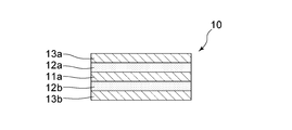
- FIG. 1 is a cross-sectional view schematically showing a structure along the thickness direction of the multilayer laminate of the present invention.
- FIG. 2 is a schematic view showing a manufacturing process of the multilayer laminate shown in FIG. 3 (a) to 3 (c) are schematic views sequentially showing steps of manufacturing a multilayer printed wiring board using the multilayer laminate board shown in FIG. 4 (a) to 4 (c) are schematic views sequentially showing steps for manufacturing a multilayer printed wiring board, continuing from FIG. 3 (c).
- 5 (a) to 5 (c) are schematic diagrams sequentially showing steps for manufacturing a multilayer printed wiring board, continuing from FIG. 4 (c).
- 6 (a) and 6 (b) are schematic diagrams sequentially showing steps for manufacturing a multilayer printed wiring board, continuing from FIG. 5 (c).
- FIGS. 8A to 8C are schematic views sequentially showing steps for manufacturing a multilayer printed wiring board, continuing from FIG. 7C.
- 9 (a) and 9 (b) are schematic views sequentially showing steps for manufacturing a multilayer printed wiring board, continuing from FIG. 8 (c).
- FIG. 1 schematically shows a cross-sectional structure along the thickness direction of a multilayer laminate 10 according to an embodiment of the present invention.
- the multilayer laminated board 10 has a five-layer structure.
- the multilayer laminate 10 has a central conductive layer 11a at the center in the thickness direction.
- a first dielectric layer 12a and a second dielectric layer 12b are disposed on each surface of the central conductive layer 11a.
- the first dielectric layer 12a and the second dielectric layer 12b are directly disposed on the surface of the central conductive layer 11a.
- no layer is interposed between the central conductive layer 11a and the first dielectric layer 12a.
- no layer is interposed between the central conductive layer 11a and the second dielectric layer 12b.
- the outer surface of the first dielectric layer 12a that is, the surface located on the side of the two main surfaces of the first dielectric layer 12a that does not face the central conductive layer 11a, is the first outer conductive layer 13a. Is arranged.
- the second outer conductive layer 13b is disposed on the outer surface of the second dielectric layer 12b.
- the first outer conductive layer 13a is directly disposed on the outer surface of the first dielectric layer 12a. In other words, no layer is interposed between the first outer conductive layer 13a and the first dielectric layer 12a.
- the second outer conductive layer 13b is disposed directly on the outer surface of the second dielectric layer 12b, and no layer is interposed between the second outer conductive layer 13b and the second dielectric layer 12b. Is not intervening.
- the first outer conductive layer 13 a and the second outer conductive layer 13 b form the outer surface of the multilayer laminate 10.
- the outer surface of the first outer conductive layer 13a that is, the surface located on the side not facing the first dielectric layer 12a out of the two main surfaces of the first outer conductive layer 13a
- the layers are also not laminated.
- the outer surface of the second outer conductive layer 13b that is, the surface located on the side not facing the second dielectric layer 12b of the two main surfaces of the first outer conductive layer 13b, no layer is formed. Is not laminated. Since the multilayer laminate 10 has the above configuration, the multilayer laminate 10 has a five-layer structure as a whole as described above.
- the first dielectric layer 12a in the multilayer laminate 10 is preferably composed of the same material at any position of the dielectric layer 12a.
- a first material arbitrarily defined and a second region arbitrarily defined different from the first region may be a constituent material. May be different.
- the constituent material of the first dielectric layer 12a and the second dielectric layer 12b These constituent materials may be the same or different.
- first outer conductive layer 13a and the second outer conductive layer 13b are preferably made of the same material at any position.
- the constituent material is composed of an arbitrarily defined first region and an arbitrarily defined second region different from the first region. It may be different.
- the constituent material of the first outer surface conductive layer 13a and the second outer surface conductive layer 13b may be the same or different.
- the central conductive layer 11 a located in the central area in the thickness direction is formed in a “solid state” over the entire area in the in-plane direction of the multilayer laminate 10.
- the central conductive layer 11a is viewed in a plan view, there is no missing portion such as a hole (through hole) or a notch in the entire thickness direction at any position.
- the central conductive layer 11a has no defect in the entire thickness direction.
- These dielectric layers 12a and 12b can be formed so that their thickness is uniform. As a result, it is possible to effectively suppress variations in the capacitances of the dielectric layers 12a and 12b.
- the degree of thickness variation is measured by the method described below.
- the multilayer laminate 10 is preferably manufactured by the method shown in FIG. Specifically, first, the central conductive layer 11a is prepared. At the same time, a first element 14a and a second element 14b are prepared. The first element 14a is formed by forming a first dielectric layer 12a on one surface of the first outer conductive layer 13a. The second element 14b is formed by forming a second dielectric layer 12b on one surface of the second outer conductive layer 13b.
- the 1st element 14a and the 2nd element 14b are arrange
- the first dielectric layer 12a in the first element 14a is opposed to the central conductive layer 11a
- the second dielectric layer 12b in the second element 14b is opposed to the central conductive layer 11a.
- Elements 14a and 14b are arranged.
- the three members are pressurized under heating in the state.
- the first element 14a and the second element 14b are pressure-bonded to each surface of the central conductive layer 11a, and the multilayer laminated board 10 formed by integrating these three elements is obtained.
- the multilayer laminate 10 can be obtained by a simple operation of simply bonding the first element 14a and the second element 14b manufactured in advance to each surface of the central conductive layer 11a, the first dielectric Variations in thickness are less likely to occur in the body layer 12a and the second dielectric layer 12b. This makes it difficult for the first dielectric layer 12a and the second dielectric layer 12b to vary in capacitance.
- Each of the first element 14a and the second element 14b is formed by applying a resin composition containing dielectric particles and a resin to one surface of each of the first outer conductive layer 13a and the second outer conductive layer 13b. It is preferably manufactured by forming the first dielectric layer 12a and the second dielectric layer 12b.
- the resin composition may be applied.
- a thermosetting resin is used as the resin
- a resin composition containing a thermosetting resin and dielectric particles in an A-stage state and in a varnish-like fluid state is used. What is necessary is just to apply.
- the 1st element 14a and the 2nd element 14b are obtained by giving a heat
- the first element 14a and the second element 14b by such a method, the first dielectric layer 12a and the second dielectric layer 12b having a uniform thickness can be successfully formed.
- thermosetting resin As the resin contained in the first dielectric layer 12a and the second dielectric layer 12b, it is preferable to use a thermosetting resin as described above, and it is particularly preferable to use a highly insulating resin.
- a thermosetting resin the thing similar to what was used until now in the technical field of a printed wiring board can be used.
- the thermosetting resin include epoxy resin, polyimide resin, polyamide resin, polyphenylene ether resin, cyanate resin, maleimide resin, phenol resin, phenoxy resin, and styrene-butadiene resin.
- the thermosetting resin is preferably in the A stage or B stage state when in the state of the first element 14a and the second element 14b, and in the state of the C stage when in the state of the multilayer laminate 10. It is preferable.
- the first dielectric layer 12a and the second dielectric layer 12b are made of a fibrous material such as a glass woven fabric, a glass nonwoven fabric and paper for reinforcing the dielectric layers 12a and 12b, or a polyimide resin, for example.
- the film-like material, that is, the reinforcing material may be included, but it is preferable that the reinforcing material is not included.
- the reinforcing material is a useful material from the viewpoint of imparting strength to the dielectric layers 12a and 12b. On the other hand, however, the use of a reinforcing material has the disadvantage that the thickness of these dielectric layers 12a and 12b increases.
- a central conductive layer 11a and metal foils to be the first and second outer conductive layers 13a and 13b are prepared, and the first and second dielectric layers 12a and 12b are prepared.
- Two dielectric resin layers are prepared, and each dielectric edge resin layer is disposed between the central conductive layer 11a and the first outer conductive layer 13a and between the central conductive layer 11a and the second outer conductive layer 13b.
- a method of obtaining the multilayer laminate 10 by heating and pressurizing under these conditions and integrating them.
- the dielectric resin layer used in this method is obtained by dispersing dielectric particles in a thermosetting resin in a B-stage state.
- the dielectric resin layer can be composed of a sheet or film containing a thermosetting resin and dielectric particles.
- the dielectric edge resin layer needs to contain a thermosetting resin and impregnate a fibrous material such as glass woven fabric, glass nonwoven fabric and paper with a thermosetting resin in a B-stage state. It may be a laminated sheet or a laminated film in which a number of sheets are stacked. A film may be used instead of the fibrous material.
- the dielectric resin layer may contain an inorganic filler.
- the dielectric resin layer is in any form, for example, an epoxy resin, a cyanate resin, a maleimide resin, a polyphenylene ether resin, a phenol resin, a polyimide resin, or the like can be used as the thermosetting resin. .
- the relative dielectric constant of the first dielectric layer 12a and the second dielectric layer 12b is preferably 10 or more, more preferably 20 or more, and still more preferably 40 or more. By setting the relative dielectric constant to be equal to or higher than these values, it is possible to easily increase the capacitance while making the dielectric layers 12a and 12b thinner. These dielectric layers 12a and 12b preferably have a higher relative dielectric constant, but considering the adhesion to the central conductive layer 11a and the first and second outer conductive layers and the strength of the dielectric layers 12a and 12b. 300 or less, more preferably 200 or less, and even more preferably 100 or less.
- the relative permittivity mentioned here is a value measured by the split post dielectric resonance method (use frequency: 1 GHz).
- the dielectric layers 12a and 12b may include the above-described dielectric particles.
- the dielectric particles those having a relative dielectric constant of 50 to 20000 are preferably used.
- a composite oxide having a perovskite structure such as a ceramic based, a lead zirconate based ceramic, a barium zirconate based ceramic, or a calcium zirconate based ceramic can be used.
- barium titanate-based ceramics are preferably used in order to obtain a high dielectric constant, but may be selectively used according to the design quality of the multilayer laminate 10.
- the dielectric particles preferably have a particle size of 0.01 ⁇ m or more and 1.0 ⁇ m or less because the dielectric constant of the dielectric layer 11 can be kept constant regardless of location.
- the particle size referred to here is the volume cumulative particle size D 50 at a cumulative volume of 50% according to the laser diffraction scattering type particle size distribution measurement method.
- the ratio of the dielectric particles contained in the first dielectric layer 12a and the second dielectric layer 12b is independent from the viewpoint of balancing the improvement in capacitance and the strength of the dielectric layers 12a and 12b. It is preferably 60% by mass to 95% by mass, more preferably 60% by mass to 90% by mass, and still more preferably 70% by mass to 90% by mass. The ratio of the dielectric particles contained in these dielectric layers 12a and 12b can be measured from the mass of the remaining particles by sublimating the resin content in the dielectric layers 12a and 12b.
- a dielectric layer that does not contain a reinforcing material and is filled with a high concentration of dielectric particles is very brittle, so when the stress at the time of lamination is high, it cannot withstand that stress and cracks. May occur.
- stacking is possible without damaging the dielectric layer.
- breaking strain energy In the stress ⁇ -strain ⁇ curve in the tensile test of the resin film forming the dielectric layer, the breaking strain energy U (unit: MJ (megajoule)) is calculated by the following integral formula.
- epsilon b shows the strain at break.
- the breaking strain energy U of the dielectric layer is more typically 1.2 MJ or less, more typically 0.8 MJ or less, and further 0.5 MJ or less.
- the lower limit value of the breaking strain energy U is not particularly limited, but if it is 0.01 MJ or more, more preferably 0.02 MJ or more, the thickness uniformity of the dielectric layers 12a and 12b in the multilayer laminate of the present invention is as follows. It can be secured sufficiently.
- the value of the breaking strain energy U is preferably satisfied by one of the dielectric layers 12a and 12b in the multilayer laminate of the present invention, and more preferably by both.
- the dielectric layer having a low breaking strain energy has a property of lowering the tensile strength.
- the tensile strength of the dielectric layer exhibiting a high relative dielectric constant is typically 60.0 MPa or less, more preferably 55.0 MPa or less, and particularly 50.0 MPa or less. The effect is exhibited more advantageously.
- the tensile strength of the dielectric layer is preferably 5.0 MPa or more, more preferably 8.0 MPa or more, from the viewpoint of sufficiently ensuring the adhesion between the dielectric layer and the conductive layer. This tensile strength value is preferably satisfied by one of the dielectric layers 12a and 12b in the multilayer laminate of the present invention, and more preferably by both.
- the dielectric layer has a low tensile elongation at break (breaking strain) of 5.0% or less, further 4.0% or less, and particularly 1.0% or less, the effect of the present invention is further enhanced. It is beneficial.
- the tensile breaking elongation (breaking strain) of the dielectric layer is preferably 0.05% or more from the viewpoint of maintaining flexibility sufficient to withstand handling at the time of manufacturing a printed wiring board. More preferably, it is 0.2% or more.
- the tensile elongation at break is preferably satisfied by one of the dielectric layers 12a and 12b in the multilayer laminate of the present invention, and more preferably by both.
- breaking strain energy, tensile strength and tensile breaking elongation are in accordance with JIS K 7161 (1994) “Plastics—Testing method for tensile properties”, measuring temperature is 25 ° C., distance between gauge points is 50 mm, and tensile speed. The value obtained from the stress-strain curve when measured at 1.0 mm / min (2% / min as the strain rate) is adopted as the standard condition. In addition, when the sample length of a dielectric material layer is remarkably short and the distance between the above-mentioned reference points cannot be taken, it can also measure by the method set to 2% / min of strain rates.
- Indentation elastic modulus Eit Another physical property value indicating the brittleness of the dielectric layer is the indentation elastic modulus Eit.
- Indentation modulus Eit dielectric layer 4800N / mm 2 or more, further 6000 N / mm 2 or more, in particular 8000 N / mm 2 or more and becomes higher the typical.
- This indentation elastic modulus Eit a value measured by a nanoindentation method in accordance with ISO14577 (2015) is adopted.
- the value of the indentation elastic modulus Eit is preferably satisfied by one of the dielectric layers 12a and 12b in the multilayer laminate of the present invention, and more preferably satisfied by both.
- the thicknesses of these dielectric layers 12a and 12b are determined at the stage of product design and circuit design, and are determined in consideration of the required level in the market. In the present invention, the thicknesses of the first dielectric layer 12a and the second dielectric layer 12b are each independently preferably 30 ⁇ m or less, more preferably 16 ⁇ m or less, particularly preferably 12 ⁇ m or less, and most preferably 8 ⁇ m or less.
- the thickness of these dielectric layers 12a and 12b there is no limitation on the lower limit of the thickness of these dielectric layers 12a and 12b, as long as the adjacent conductive layers are not short-circuited.
- it is preferably 0.1 ⁇ m or more independently, and more preferably 0.5 ⁇ m or more in order to prevent the above-described short circuit more reliably.
- the first dielectric layer 12a and the second dielectric layer 12b each have a small variation in thickness measured at a plurality of arbitrary positions, provided that the first dielectric layer 12a and the second dielectric layer 12b have a thickness in the above-described range. This is because variation in the thickness of the capacitors formed from these dielectric layers 12a and 12b is less likely to occur due to the small variation in thickness. From this viewpoint, the dielectric layers 12a and 12b each have a thickness variation of preferably 15% or less, more preferably 10% or less, and still more preferably 8% or less.
- the variation in the thickness of these dielectric layers 12a and 12b is a cross section in the thickness direction of the center of the first dielectric layer 12a or the second dielectric layer 12b and its end portions (for example, four corners if the dielectric layer is rectangular).
- Magnified observation for example, magnification of 500 times or more to measure a total of at least 10 points, find the maximum value, minimum value, and average value, numerical values (units) represented by the following (1) and (2) :%) Is a value defined by a numerical value with a large value. [100 ⁇ (maximum value ⁇ average value) / average value] (1) [100 ⁇ (average value ⁇ minimum value) / average value] (2)
- each of the first dielectric layer 12a and the second dielectric layer 12b has a small thickness variation.
- the first dielectric layer 12a and the second dielectric layer 12b may have the same thickness or may be different.
- the difference between the relative dielectric constant of the first dielectric layer 12a and the relative dielectric constant of the second dielectric layer 12b is preferably small.
- the difference between the relative dielectric constant ⁇ a of the first dielectric layer 12a and the relative dielectric constant ⁇ b of the second dielectric layer 12b is preferably 10% or less, more preferably 5% or less, and 3%. More preferably, it is as follows.
- the difference between the relative dielectric constants ⁇ a and ⁇ b of both the dielectric layers 12a and 12b is small, the design when manufacturing the multilayer printed wiring board using the multilayer laminated board 10 becomes easy. From this viewpoint, it is particularly preferable that the first dielectric layer 12a and the second dielectric layer 12b have the same thickness. It is particularly preferable that the first dielectric layer 12a and the second dielectric layer 12b have the same composition (composition of the resin composition) constituting them.
- the difference between the relative dielectric constants ⁇ a and ⁇ b of both dielectric layers 12a and 12b is defined by [(
- the central conductive layer 11a, the first outer conductive layer 13a, and the second outer conductive layer 13b sandwiching the first dielectric layer 12a and the second dielectric layer 12b are not particularly limited in thickness, and may be thin or thick. Also good.
- the thicknesses of these conductive layers 11a, 13a, and 13b are preferably set independently from, for example, 0.1 ⁇ m to 70 ⁇ m.
- the thicknesses and / or types of the conductive layers 11a, 13a, and 13b may be the same or different.
- these conductive layers 11a, 13a, and 13b are preferably made of metal foil from the viewpoint of the manufacturing process. Such metal foil may be any of rolled foil, electrolytic foil, and vapor phase foil.
- the metal foil is a copper foil, but other metal foils may be used.
- the conductive layers 13a and 13b may be provided with an electric resistance layer (for example, a layer made of Ni-P, Ni-Cr, etc.) on the surface facing the dielectric layer 12.
- the dielectric layer The roughness of the surface facing 12a, 12b is preferably low. From this point of view, the opposing surfaces of the first and second dielectric layers 12a, 12b in the conductive layers 11a, 13a, 13b have their surface roughness expressed by a ten-point average roughness Rz (JIS B0601-1994). Rz is preferably 1.5 ⁇ m or less, more preferably 1.0 ⁇ m or less, and even more preferably no roughening treatment.
- the central conductive layer 11a preferably has a difference in Rz between both surfaces of 1.0 ⁇ m or less, and more preferably 0.5 ⁇ m or less. Since the central conductive layer 11a faces both the dielectric layers 12a and 12b, the thickness of the first and second dielectric layers 12a and 12b is reduced by reducing the difference in roughness between the both surfaces of the central conductive layer 11a. Can be made more uniform.
- the multilayer laminated board 10 having the configuration as described above is suitably used as a material for manufacturing a multilayer printed wiring board. Accordingly, a preferred method for manufacturing a multilayer printed wiring board using the multilayer laminate 10 will be described below.
- first through holes 15 penetrating the multilayer laminated plate 10 over the entire thickness direction are formed at predetermined positions in the multilayer laminated plate 10.
- a drilling means known in the technical field such as a drill can be used as appropriate.
- an appropriate value is selected according to the specific use of the target multilayer printed wiring board.
- a filler 16 is filled into the first through hole 15 formed by perforation.
- a non-conductive material is preferably used.
- the non-conductive material here means a volume resistivity of the material is 1 ⁇ 10 7 ⁇ ⁇ cm or more at 25 ° C..
- it is easy to use a resin and it is particularly preferable to use various thermosetting resins exemplified as the resins constituting the dielectric layers 12a and 12b.
- the first through hole 15 is filled with a thermosetting resin in an A-stage state, and this is then cured.
- a filler 16 made of a cured resin is formed in the first through hole 15.
- the first through hole 15 is completely filled with the filler 16.
- the second through hole 17 is formed as shown in FIG.
- the second through hole 17 is formed at a position where the filler 16 is filled.
- the second through-hole 17 is formed so as to penetrate the multilayer laminate 10 in the thickness direction.
- the shape of the second through hole 17 is preferably similar to the shape of the first through hole 15.
- the second through hole 17 and the first through hole 15 are both circular (true circles).
- the second through hole 17 has a smaller diameter than the first through hole 15.
- the second through hole 17 is preferably formed so that the centroid of the first through hole 15 and the centroid of the second through hole 17 coincide with each other in plan view of the multilayer laminate 10.
- the second through hole 17 and the first through hole 15 in the plan view of the multilayer laminate 10 are both circular
- the second through hole is so arranged that the through holes 17 and 15 are concentric. 17 is preferably formed.
- the shape of the filler 16 after the second through hole 17 is formed changes from a columnar shape to a cylindrical shape. Therefore, the inner wall of the second through hole 17 is made of a nonconductive material.
- the third conductive layers 18a and 18b are formed on the outer surfaces of the first and second outer conductive layers 13a and 13b in the multilayer laminate 10.
- a fourth conductive layer 19 is formed on the inner wall of the second through hole 17.
- the fourth conductive layer 19 is formed so as to be electrically connected to the two third conductive layers 18a and 18b. Since the 4th conductive layer 19 is formed in the surface of the filler 16 comprised from a nonelectroconductive material, the 4th conductive layer 19 and the center conductive layer 11a are insulated with a filler, and become non-conducting.
- an electroless plating method is used to form the third conductive layers 18a and 18b and the fourth conductive layer 19, but the method is not limited thereto.
- patterning for circuit formation is performed on the multilayer laminate 10.
- a process of forming a circuit by patterning the first and second outer conductive layers 13a and 13b including the third conductive layers 18a and 18b is shown.
- various lithography methods known in the art can be appropriately used.
- the third conductive layers 18a and 18b and the first and second outer conductive layers 13a and 13b are partially removed for patterning, the first conductive layer 13a is at least one of the removed portions on the first outer conductive layer 13a side. It is preferable to perform patterning so that the first missing portion Ra and the second missing portion Rb, which is at least one of the removed portions on the second outer surface conductive layer 13b side, overlap in a plan view of the multilayer laminate 10. .
- the insulating resin layer 20 is laminated on each surface of the multilayer laminate 10 as shown in FIG.
- the resin contained in the insulating resin layer 20 serves as a filler, so that the inside of the second through hole 17 is completely filled, and each surface of the multilayer laminate 10 is completely covered with the insulating resin layer 20.
- the insulating resin layer 20 those known in the technical field can be used without particular limitation. Since the insulating resin layer 20 generally includes a B-stage thermosetting resin as a non-conductive material, in the lamination using the insulating resin layer 20, the insulating resin layer 20 is heated to produce the insulating resin layer 20.
- the layer 20 is preferably bonded to the multilayer laminate 10.
- the insulating resin layer may be (a) a required number of prepregs impregnated with an insulating resin in a fibrous material such as glass woven fabric, glass nonwoven fabric and paper.
- the insulating resin to be impregnated include epoxy resin, cyanate resin, maleimide resin, polyphenylene ether resin, phenol resin, and polyimide resin.
- an insulating resin layer (that is, a layer not including a fibrous material) made of an insulating resin such as an epoxy resin, a polyimide resin, or a polyester resin may be used.
- the inorganic filler in the insulating resin layer can be contained.
- the filler filled in the second through hole 17 is an insulating resin and an inorganic filler.
- the fifth conductive layers 21a and 21b are formed on each surface of the insulating resin layer 20, respectively.
- Both the fifth conductive layers 21a and 21b can be made of, for example, a metal foil.
- the insulating resin layers 20 and 20 and the fifth conductive layers 21a and 21b can be stacked by various methods. For example, first, the semi-cured B-stage insulating resin layers 20 and 20 are laminated on each surface of the multilayer laminate 10, and the fifth conductive layers 21a and 21b are laminated thereon. Then, the insulating resin layer 20 is cured by pressing under heating, and these three are joined and integrated. Further, instead of separately preparing the insulating resin layers 20 and 20 and the fifth conductive layers 21a and 21b, these layers may be laminated with a metal foil with resin.
- patterning is performed on the fifth conductive layer 21b. This patterning is performed in order to form a conformal mask for drilling the insulating resin layer 20. A part of the fifth conductive layer 21b is removed by patterning to form a third missing portion Rc.
- the insulating resin layer 20 is punched with a laser beam through the missing portion Rc removed by the patterning in the fifth conductive layer 21b. Drilling the insulating resin layer 20 is performed so that the third conductive layer 18b is exposed.
- the third through hole 22 penetrating over the entire thickness direction is formed as shown in FIG. 5C.
- the third through hole 22 is formed by removing the conductive layers 13a and 13b from the circuit pattern formed on the first outer conductive layers 13a and 13b in the step shown in FIG. This is performed for the first missing portion Ra and the second missing portion Rb, which are the formed portions.
- sixth conductive layers 23a and 23b are formed on the outer surfaces of the fifth conductive layers 21a and 21b as shown in FIG.
- the sixth conductive layer 23b is also formed on the side surface of the hole 25 formed in the fifth conductive layer 21b and the insulating resin layer 20, and connects the sixth conductive layer 23b and the exposed third conductive layer 18b.
- a seventh conductive layer 24 is formed on the inner wall of the third through hole 22.
- the seventh conductive layer 24 is formed so as to be electrically connected to the two sixth conductive layers 23a and 23b.
- the seventh conductive layer 24 is formed on the side surface of the third through hole 22 so as to be electrically connected to the fifth conductive layers 21a and 21b and the central conductive layer 11a.
- an electroless plating method is used to form the sixth conductive layers 23a and 23b and the seventh conductive layer 24, but the method is not limited thereto.
- the connection between the sixth conductive layer 23b and the seventh conductive layer 24 is disconnected.
- the cutting can be performed, for example, by patterning the sixth conductive layer 23b.
- the cut portion is on the fifth conductive layer 21b.
- known means such as laser light irradiation or etching can be used.
- a hole 26 is formed in the sixth conductive layer 23b and the fifth conductive layer 21b in the thickness direction so that the surface of the insulating resin layer 20 is exposed. As a result, the connection between the sixth conductive layer 23b and the fifth conductive layer 21b and the seventh conductive layer 24 is disconnected.
- the first and second dielectric layers 12a and 12b are respectively composed of the central conductive layer 11a and the first and second outer conductive layers.
- a built-in capacitor is formed by being disposed between 13a and 13b.
- the central conductive layer 11 a is connected to the sixth conductive layer 23 a exposed on one surface of the multilayer printed wiring board 100 through the seventh conductive layer 24.
- the first and second outer conductive layers 13 a and 13 b are connected to the sixth conductive layer 23 b exposed on the other surface of the multilayer printed wiring board 100 through the third conductive layers 18 a and 18 b and the fourth conductive layer 19. Connected. Therefore, the built-in capacitor can function by applying a voltage between the sixth conductive layers 23a and 23b.
- the multilayer printed wiring board 100 having the built-in capacitors can be obtained without impairing the thickness uniformity of the first and second dielectric layers 12 a and 12 b. Therefore, this built-in capacitor has a suppressed variation in its capacitance. Further, the central conductive layer 11a and the first and second outer conductive layers 13a and 13b in the multilayer laminate 10 can be easily connected to an external conductive layer.
- the manufacturing method of this embodiment is the same process up to FIG. 3A in the above-described embodiment. Then, after the step shown in FIG. 3A, patterning for circuit formation is performed on the multilayer laminate 10 as shown in FIG. 7A. In the figure, a step of patterning the first and second outer conductive layers 13a and 13b to form a circuit is shown.
- the first missing portion Ra which is at least one of the removed portions on the first outer conductive layer 13a side
- the second missing portion Rb which is at least one of the removed portions on the outer surface conductive layer 13b side
- the insulating resin layer 20 is laminated on each surface of the multilayer laminate 10 as shown in FIG. Thereby, the resin contained in the insulating resin layer 20 serves as a filler, and the first through hole 15 is completely filled, and each surface of the multilayer laminate 10 is completely covered with the insulating resin layer 20.
- the insulating resin layer 20 can contain an inorganic filler as in the embodiment shown in FIG.
- the filler filled in the first through hole 15 is an insulating resin and an inorganic filler.
- the fifth conductive layers 21a and 21b are patterned. This patterning is performed in order to form a conformal mask for drilling the insulating resin layer 20. Part of the fifth conductive layers 21a and 21b is removed by patterning to form a third missing portion Rc.
- a laser is applied to the insulating resin layer 20 through the third missing portion Rc (see FIG. 7C) of the fifth conductive layers 21a and 21b removed by the patterning. Drilling with light. Drilling into the insulating resin layer 20 is performed so that the first and second outer conductive layers 13a and 13b are exposed.
- the second through hole 17 is formed.
- the second through hole 17 is formed at a position where the first through hole 15 is filled with the insulating resin layer 20.
- the second through hole 17 is formed so as to penetrate through the multilayer laminated plate 10 in the entire thickness direction.
- the second through hole 17 has a smaller diameter than the first through hole 15.
- the second through hole 17 is preferably formed so that the centroid of the first through hole 15 and the centroid of the second through hole 17 coincide with each other in plan view of the multilayer laminate 10.
- the shape of the insulating resin layer 20 in the first through hole 15 after the second through hole 17 is formed changes from a columnar shape to a cylindrical shape. Therefore, the inner wall of the second through hole 17 is made of a non-conductive material.
- the third through hole 22 is formed.
- the third through hole 22 is formed so as to penetrate through the entire thickness direction of the multilayer laminate 10.
- the formation of the third through hole 22 is performed, for example, by removing the conductive layers 13a and 13b from the circuit pattern formed on the first outer conductive layers 13a and 13b in the step shown in FIG. This is performed for the first missing portion Ra and the second missing portion Rb, which are the formed portions.
- the diameter of the third through hole 22 is preferably the same as the diameter of the second through hole 17 formed previously.
- the third conductive layers 18a and 18b are formed on the outer surfaces of the fifth conductive layers 21a and 21b as shown in FIG. 9A.
- the third conductive layers 18a and 18b are also formed on the side surfaces of the holes 25 formed in the fifth conductive layer 21b and the insulating resin layer 20, and the third conductive layers 18a and 18b and the exposed first and first conductive layers are formed.
- the outer surface conductive layers 13a and 13b are connected.
- the fourth conductive layer 19 is formed on the inner wall of the second through hole 17, and the seventh conductive layer 24 is formed on the inner wall of the third through hole 22.
- the fourth conductive layer 19 is formed so as to be electrically connected to the two third conductive layers 18a and 18b.
- the seventh conductive layer 24 is formed to be electrically connected to the two third conductive layers 18a and 18b. Since the fourth conductive layer 19 is formed on the surface of the insulating resin layer 20 made of a nonconductive material, the fourth conductive layer 19 and the central conductive layer 11a are insulated by the insulating resin layer 20 and become non-conductive. . On the other hand, since the seventh conductive layer 24 is formed directly on the inner wall of the third through hole 22, the central conductive layer 11a exposed on the inner wall of the third through hole 22 and the seventh conductive layer 24 are electrically connected. .
- the connection between the third conductive layers 18a and 18b and the seventh conductive layer 24 is disconnected.
- the cutting can be performed, for example, by patterning the third conductive layers 18a and 18b by etching or the like.
- the locations where these connections are disconnected are on the fifth conductive layers 21a and 21b.
- holes 26 are formed in the third conductive layers 18a and 18b and the fifth conductive layers 21a and 21b in the thickness direction so that the surface of the insulating resin layer 20 is exposed. To do.
- the connection between the third conductive layers 18 a and 18 b and the fifth conductive layers 21 a and 21 b and the seventh conductive layer 24 is disconnected.
- the first and second dielectric layers 12a and 12b are respectively composed of the central conductive layer 11a and the first and second outer conductive layers.
- a built-in capacitor is formed by being disposed between 13a and 13b.
- the central conductive layer 11 a is connected to the third conductive layers 18 a ′ and 18 b ′ exposed on the outer surface of the multilayer printed wiring board 100 through the seventh conductive layer 24.
- the first and second outer conductive layers 13a and 13b are directly connected to the third conductive layers 18a "and 18b". Therefore, the built-in capacitor can function by applying a voltage between the third conductive layers 18a 'and 18b' and the third conductive layers 18a "and 18b".
- the use of the multilayer laminated board 10 makes it possible to incorporate the first and second dielectric layers 12a and 12b without impairing the thickness uniformity.
- a multilayer printed wiring board 100 having a capacitor is obtained. Therefore, this built-in capacitor has a suppressed variation in its capacitance.
- the third missing portion Rc is formed by removing a part of the fifth conductive layers 21a and 21b in order to form a conformal mask.
- the third missing portion Rc may not be formed.
- the third through hole 22 is formed after the second through hole 17 is formed, but this order may be reversed. Alternatively, the second through hole 17 and the third through hole 22 may be formed simultaneously. These through holes 17 and 22 can generally be formed using a drill.
- a multilayer laminated board in which the variation in the capacitance of the built-in capacitor is suppressed.
Landscapes
- Engineering & Computer Science (AREA)
- Microelectronics & Electronic Packaging (AREA)
- Manufacturing & Machinery (AREA)
- Chemical & Material Sciences (AREA)
- Inorganic Chemistry (AREA)
- Power Engineering (AREA)
- Ceramic Engineering (AREA)
- Production Of Multi-Layered Print Wiring Board (AREA)
- Laminated Bodies (AREA)
Abstract
Description
前記多層積層板においては、第1外面導電層及び第2外面導電層が、該多層積層板の外面をなし、
前記中央導電層は、前記多層積層板の面内方向の全域にわたり、べた状態で形成されており、
第1誘電体層の厚みのばらつき及び第2誘電体層の厚みのばらつきが、それぞれ独立に15%以下である、多層積層板を提供するものである。
前記多層積層板をその厚み方向に貫通する第1スルーホールを形成し、
形成された第1スルーホール内に非導電性の充填剤を完全充填し、
第1スルーホールよりも小径の第2スルーホールを、前記充填剤が充填された位置に、前記多層積層板の厚み方向に貫通するように形成する、工程を有する多層プリント配線板の製造方法を提供するものである。
前記脆さを示す物性値としては、破断ひずみエネルギーを採用することが好適である。誘電体層を形成する樹脂フィルムの引張試験における応力σ-ひずみε曲線において、破断ひずみエネルギーU(単位:MJ(メガジュール))は、下記積分式によって算出される。なお、εbは破断時のひずみを示す。

一方で、誘電体層と、導電層との密着性を十分に確保する点では、誘電体層の引張強度は、5.0MPa以上であることが好ましく、より好ましくは8.0MPa以上である。
この引張強度の値は、本発明の多層積層板における誘電体層12a,12bのいずれか一方で満たされることが好ましく、双方で満たされることが更に好ましい。
一方で、プリント配線板製造時のハンドリングに最低限耐え得るだけの可撓性を保持する点では、誘電体層の引張破断伸び率(破断ひずみ)は、0.05%以上であることが好ましく、より好ましくは0.2%以上である。
この引張破断伸び率の値は、本発明の多層積層板における誘電体層12a,12bのいずれか一方で満たされることが好ましく、双方で満たされることが更に好ましい。
なお、上述した破断ひずみエネルギー、引張強度及び引張破断伸び率は、JISK7161(1994)「プラスチック-引張特性の試験方法」に準拠し、測定温度を25℃、標点間の距離を50mm、引張速度を1.0mm/min(ひずみ速度として2%/min)で測定したときの応力ひずみ曲線から求めた値を標準条件として採用するものとする。なお、誘電体層の試料長が著しく短く、上述した標点間の距離が取れない場合は、ひずみ速度2%/minとした方法で測定することも可能である。
これらの誘電体層12a,12bの厚みのばらつきは、第1誘電体層12a又は第2誘電体層12bの中心とその端部(例えば誘電体層が矩形であれば四隅)の厚み方向の断面を拡大観察(例えば500倍以上に拡大)することで合計で最低10点を測定し、その最大値、最小値及び平均値を求め、下記(1)及び(2)で表される数値(単位:%)のうち、値の大きい数値によって定義される値である。
〔100×(最大値-平均値)/平均値〕 (1)
〔100×(平均値-最小値)/平均値〕 (2)
絶縁樹脂層20,20及び第5導電層21a,21bの積層は種々の方法で行うことができる。例えば、まず多層積層板10の各面に対して、半硬化のBステージ状態の絶縁樹脂層20,20を積層するとともに、その上に第5導電層21a,21bを積層する。そして、加熱下にプレスすることで絶縁樹脂層20が硬化してこれら三者が接合一体化される。また、絶縁樹脂層20,20及び第5導電層21a,21bを別途用意することに代えて、これらの積層を樹脂付金属箔によって行ってもよい。
11a 中央導電層
12a 第1誘電体層
12b 第2誘電体層
13a 第1外面導電層
13b 第2外面導電層
14a 第1エレメント
14b 第2エレメント
15 第1スルーホール
16 充填剤
17 第2スルーホール
18a,18b 第3導電層
19 第4導電層
20 絶縁樹脂層
21a,21b 第5導電層
22 第3スルーホール
23a,23b 第6導電層
24 第7導電層
25,26 穴
100 多層プリント配線板
Ra 第1欠落部
Rb 第2欠落部
Rc 第3欠落部
Claims (9)
- 中央導電層と、該中央導電層の各面にそれぞれ直接配置された第1誘電体層及び第2誘電体層と、第1誘電体層の外側に直接配置された第1外面導電層と、第2誘電体層の外側に直接配置された第2外面導電層とを備えた多層積層板であって、
前記多層積層板においては、第1外面導電層及び第2外面導電層が、該多層積層板の外面をなし、
前記中央導電層は、前記多層積層板の面内方向の全域にわたり、べた状態で形成されており、
第1誘電体層の厚みのばらつき及び第2誘電体層の厚みのばらつきが、それぞれ独立に15%以下である、多層積層板。 - 第1誘電体層の比誘電率と第2誘電体層の比誘電率との差が10%以下である請求項1に記載の多層積層板。
- 第1誘電体層の厚み及び第2誘電体層の厚みが、それぞれ独立に0.1μm以上30μm以下である請求項1又は2に記載の多層積層板。
- 第1誘電体層の厚みと第2誘電体層の厚みとが同じである請求項3に記載の多層積層板。
- 第1誘電体層及び第2誘電体層がそれぞれ誘電体粒子及び樹脂を含み、これらの誘電体層に占める該誘電体粒子の割合が、それぞれ独立に60質量%以上95質量%以下である請求項1ないし4のいずれか一項に記載の多層積層板。
- 第1誘電体層の組成と第2の誘電体層の組成とが同じである請求項5に記載の多層積層板。
- 第1誘電体層及び第2誘電体層の応力σ-ひずみε曲線における破断ひずみエネルギーが、それぞれ1.8MJ以下である、請求項1ないし6のいずれか一項に記載の多層積層板。
- 前記各導電層がいずれも銅箔からなり、その厚みがそれぞれ独立に0.1μm以上70μm以下である請求項1ないし7のいずれか一項に記載の多層積層板。
- 請求項1に記載の多層積層板を用意し、
前記多層積層板をその厚み方向に貫通する第1スルーホールを形成し、
形成された第1スルーホール内に非導電性の充填剤を完全充填し、
第1スルーホールよりも小径の第2スルーホールを、前記充填剤が充填された位置に、前記多層積層板の厚み方向に貫通するように形成する、工程を有する多層プリント配線板の製造方法。
Priority Applications (5)
| Application Number | Priority Date | Filing Date | Title |
|---|---|---|---|
| MYPI2018702988A MY191270A (en) | 2016-03-10 | 2017-02-03 | Multilayer laminate and method for producing multilayer printed wiring board using same |
| CN201780015169.6A CN108781517B (zh) | 2016-03-10 | 2017-02-03 | 多层层叠板以及使用其的多层印刷电路板的制造方法 |
| KR1020187024746A KR102737460B1 (ko) | 2016-03-10 | 2017-02-03 | 다층 적층판 및 이것을 이용한 다층 프린트 배선판의 제조 방법 |
| US16/082,393 US11285700B2 (en) | 2016-03-10 | 2017-02-03 | Multilayer laminate and method for producing multilayer printed wiring board using same |
| JP2018504056A JP6916165B2 (ja) | 2016-03-10 | 2017-02-03 | 多層積層板及びこれを用いた多層プリント配線板の製造方法 |
Applications Claiming Priority (2)
| Application Number | Priority Date | Filing Date | Title |
|---|---|---|---|
| PCT/JP2016/057563 WO2017154167A1 (ja) | 2016-03-10 | 2016-03-10 | 多層積層板及びこれを用いた多層プリント配線板の製造方法 |
| JPPCT/JP2016/057563 | 2016-03-10 |
Publications (1)
| Publication Number | Publication Date |
|---|---|
| WO2017154432A1 true WO2017154432A1 (ja) | 2017-09-14 |
Family
ID=59789155
Family Applications (2)
| Application Number | Title | Priority Date | Filing Date |
|---|---|---|---|
| PCT/JP2016/057563 Ceased WO2017154167A1 (ja) | 2016-03-10 | 2016-03-10 | 多層積層板及びこれを用いた多層プリント配線板の製造方法 |
| PCT/JP2017/003966 Ceased WO2017154432A1 (ja) | 2016-03-10 | 2017-02-03 | 多層積層板及びこれを用いた多層プリント配線板の製造方法 |
Family Applications Before (1)
| Application Number | Title | Priority Date | Filing Date |
|---|---|---|---|
| PCT/JP2016/057563 Ceased WO2017154167A1 (ja) | 2016-03-10 | 2016-03-10 | 多層積層板及びこれを用いた多層プリント配線板の製造方法 |
Country Status (7)
| Country | Link |
|---|---|
| US (1) | US11285700B2 (ja) |
| JP (1) | JP6916165B2 (ja) |
| KR (1) | KR102737460B1 (ja) |
| CN (1) | CN108781517B (ja) |
| MY (1) | MY191270A (ja) |
| TW (1) | TWI702621B (ja) |
| WO (2) | WO2017154167A1 (ja) |
Families Citing this family (5)
| Publication number | Priority date | Publication date | Assignee | Title |
|---|---|---|---|---|
| KR102927896B1 (ko) * | 2018-08-30 | 2026-02-13 | 미츠비시 가스 가가쿠 가부시키가이샤 | 적층체, 금속박 피복 적층판, 패터닝된 금속박이 부착된 적층체, 빌드업 구조를 갖는 적층체, 프린트 배선판, 다층 코어리스 기판, 및 그 제조 방법 |
| CN117120536A (zh) * | 2021-03-24 | 2023-11-24 | 松下知识产权经营株式会社 | 树脂组合物、预浸料、带树脂的膜、带树脂的金属箔、覆金属箔层压板、以及布线板 |
| EP4081005A1 (en) | 2021-04-23 | 2022-10-26 | AT & S Austria Technologie & Systemtechnik Aktiengesellschaft | Component carrier |
| WO2023218801A1 (ja) * | 2022-05-13 | 2023-11-16 | 株式会社村田製作所 | コンデンサ |
| US12250771B2 (en) | 2022-07-21 | 2025-03-11 | Rockwell Collins, Inc. | Capacitor bank assembly |
Citations (4)
| Publication number | Priority date | Publication date | Assignee | Title |
|---|---|---|---|---|
| JP2006210536A (ja) * | 2005-01-26 | 2006-08-10 | Ngk Spark Plug Co Ltd | 電子部品の製造方法、電子部品付き配線基板 |
| JP2007184386A (ja) * | 2006-01-06 | 2007-07-19 | Matsushita Electric Works Ltd | 誘電体層付導電性基材、その製造方法、キャパシタ及びプリント配線基板 |
| JP2009004457A (ja) * | 2007-06-19 | 2009-01-08 | Taiyo Yuden Co Ltd | コンデンサ内蔵多層基板 |
| JP2009043769A (ja) * | 2007-08-06 | 2009-02-26 | Ngk Spark Plug Co Ltd | コンデンサ内蔵配線基板及びその製造方法、支持体付きコンデンサ |
Family Cites Families (144)
| Publication number | Priority date | Publication date | Assignee | Title |
|---|---|---|---|---|
| GB690328A (en) * | 1948-10-20 | 1953-04-15 | Strong Harold Vezey | Improvements relating to electric capacitors and printed circuits containing capacitors |
| US2593829A (en) * | 1949-01-13 | 1952-04-22 | Bayer Ag | Electrical capacitor and foil therefor |
| JPH023631Y2 (ja) * | 1984-12-28 | 1990-01-29 | ||
| US4996097A (en) * | 1989-03-16 | 1991-02-26 | W. L. Gore & Associates, Inc. | High capacitance laminates |
| US5155655A (en) * | 1989-08-23 | 1992-10-13 | Zycon Corporation | Capacitor laminate for use in capacitive printed circuit boards and methods of manufacture |
| KR920700460A (ko) * | 1989-09-21 | 1992-02-19 | 마에다 가쯔노스께 | 필름콘덴서 및 그의 제조방법 |
| JPH0793496B2 (ja) * | 1990-10-04 | 1995-10-09 | 日立化成工業株式会社 | 銅張積層板用銅箔樹脂接着層 |
| AU2392592A (en) * | 1992-07-16 | 1994-02-14 | Zycon Corporation | Printed circuit board with internal capacitor |
| US5530288A (en) * | 1994-10-12 | 1996-06-25 | International Business Machines Corporation | Passive interposer including at least one passive electronic component |
| US5509200A (en) * | 1994-11-21 | 1996-04-23 | International Business Machines Corporation | Method of making laminar stackable circuit board structure |
| US5604167A (en) * | 1995-10-16 | 1997-02-18 | Ferro Corporation | Y5V dielectric composition |
| US5847327A (en) * | 1996-11-08 | 1998-12-08 | W.L. Gore & Associates, Inc. | Dimensionally stable core for use in high density chip packages |
| JPH11207870A (ja) * | 1998-01-27 | 1999-08-03 | Nitto Denko Corp | 金属箔張回路用基板およびこれを用いてなる回路板ならびに金属箔張回路板 |
| JP3614644B2 (ja) * | 1998-02-27 | 2005-01-26 | 松下電器産業株式会社 | 積層体の製造方法 |
| US20020048137A1 (en) * | 1998-04-01 | 2002-04-25 | Williams Thomas J. | Two-layered embedded capacitor |
| US6608760B2 (en) * | 1998-05-04 | 2003-08-19 | Tpl, Inc. | Dielectric material including particulate filler |
| US20040109298A1 (en) * | 1998-05-04 | 2004-06-10 | Hartman William F. | Dielectric material including particulate filler |
| JP2000133947A (ja) * | 1998-10-27 | 2000-05-12 | Toppan Printing Co Ltd | 多層プリント配線板用絶縁層樹脂組成物 |
| US6215649B1 (en) * | 1998-11-05 | 2001-04-10 | International Business Machines Corporation | Printed circuit board capacitor structure and method |
| JP2000244130A (ja) * | 1998-12-25 | 2000-09-08 | Ngk Spark Plug Co Ltd | 配線基板、コア基板及びその製造方法 |
| US6274224B1 (en) * | 1999-02-01 | 2001-08-14 | 3M Innovative Properties Company | Passive electrical article, circuit articles thereof, and circuit articles comprising a passive electrical article |
| US6613413B1 (en) * | 1999-04-26 | 2003-09-02 | International Business Machines Corporation | Porous power and ground planes for reduced PCB delamination and better reliability |
| US6291779B1 (en) * | 1999-06-30 | 2001-09-18 | International Business Machines Corporation | Fine pitch circuitization with filled plated through holes |
| JP2001094265A (ja) * | 1999-09-24 | 2001-04-06 | Sumitomo Bakelite Co Ltd | 多層プリント配線板用絶縁樹脂付き銅箔 |
| US6562179B1 (en) * | 1999-11-04 | 2003-05-13 | Mitsubishi Gas Chemical Company, Inc. | High relative-permittivity B-staged sheet, high relative-permittivity prepreg, its production process, and printed wiring board comprising any one of these |
| US6480370B1 (en) * | 1999-12-28 | 2002-11-12 | Intel Corporation | Polymeric dielectric material for high-energy density capacitors |
| JP2001192536A (ja) * | 2000-01-11 | 2001-07-17 | Mitsubishi Gas Chem Co Inc | 高比誘電率bステージシート、それを用いたプリント配線板 |
| JP2001261861A (ja) * | 2000-03-17 | 2001-09-26 | Hitachi Chem Co Ltd | プリプレグの製造方法、プリプレグ、金属張り積層板及び印刷配線板 |
| US6467160B1 (en) * | 2000-03-28 | 2002-10-22 | International Business Machines Corporation | Fine pitch circuitization with unfilled plated through holes |
| EP1269808B1 (en) * | 2000-03-31 | 2007-08-22 | Dyconex AG | Method for fabricating electrical connecting elements, and connecting element |
| JP2001347600A (ja) * | 2000-06-06 | 2001-12-18 | Matsushita Electric Works Ltd | 積層板 |
| US6657849B1 (en) * | 2000-08-24 | 2003-12-02 | Oak-Mitsui, Inc. | Formation of an embedded capacitor plane using a thin dielectric |
| JP4529262B2 (ja) * | 2000-09-14 | 2010-08-25 | ソニー株式会社 | 高周波モジュール装置及びその製造方法 |
| JP2002117738A (ja) * | 2000-10-06 | 2002-04-19 | Korea Inst Of Science & Technology | 高分子マトリックスを用いた誘電体セラミックス厚膜の製造方法 |
| JP2002260959A (ja) * | 2001-03-01 | 2002-09-13 | Nec Corp | 積層コンデンサとその製造方法およびこのコンデンサを用いた半導体装置、電子回路基板 |
| SG99360A1 (en) * | 2001-04-19 | 2003-10-27 | Gul Technologies Singapore Ltd | A method for forming a printed circuit board and a printed circuit board formed thereby |
| US6756628B2 (en) * | 2001-05-30 | 2004-06-29 | Matsushita Electric Industrial Co., Ltd. | Capacitor sheet with built in capacitors |
| JP2003011270A (ja) * | 2001-07-02 | 2003-01-15 | Jsr Corp | 導電性箔付き誘電体層およびこれを用いたコンデンサ、ならびにその形成方法 |
| JP2003031719A (ja) * | 2001-07-16 | 2003-01-31 | Shinko Electric Ind Co Ltd | 半導体パッケージ及びその製造方法並びに半導体装置 |
| JP3770537B2 (ja) * | 2001-07-30 | 2006-04-26 | 三井金属鉱業株式会社 | キャパシター及びそれを形成するための両面銅張積層板の製造方法 |
| JP4148501B2 (ja) * | 2002-04-02 | 2008-09-10 | 三井金属鉱業株式会社 | プリント配線板の内蔵キャパシタ層形成用の誘電体フィラー含有樹脂及びその誘電体フィラー含有樹脂を用いて誘電体層を形成した両面銅張積層板並びにその両面銅張積層板の製造方法 |
| JP2003318510A (ja) * | 2002-04-23 | 2003-11-07 | Matsushita Electric Works Ltd | インピーダンス検査用積層板及びその製造方法並びにインピーダンス検査用積層板のインピーダンス測定方法 |
| JP4080799B2 (ja) * | 2002-06-28 | 2008-04-23 | 三井金属鉱業株式会社 | 金属材表面への誘電体フィラー含有ポリイミド被膜の形成方法並びにプリント配線板用のキャパシタ層形成用の銅張積層板の製造方法及びその製造方法で得られた銅張積層板 |
| JP4488684B2 (ja) * | 2002-08-09 | 2010-06-23 | イビデン株式会社 | 多層プリント配線板 |
| JP2004134421A (ja) * | 2002-10-08 | 2004-04-30 | Nec Tokin Corp | コンデンサ内蔵配線基板及びその製造方法 |
| KR100482822B1 (ko) * | 2002-10-24 | 2005-04-14 | 대덕전자 주식회사 | 캐패시터 내장형 인쇄 회로 기판 제조 방법 |
| KR100455890B1 (ko) * | 2002-12-24 | 2004-11-06 | 삼성전기주식회사 | 커패시터 내장형 인쇄회로기판 및 그 제조 방법 |
| TWI262204B (en) * | 2003-05-14 | 2006-09-21 | Eternal Chemical Co Ltd | Resin composition having high dielectric constant and uses thereof |
| JP4300890B2 (ja) * | 2003-06-11 | 2009-07-22 | 日立化成工業株式会社 | 多層配線板の製造方法 |
| US7164197B2 (en) * | 2003-06-19 | 2007-01-16 | 3M Innovative Properties Company | Dielectric composite material |
| JP4274861B2 (ja) * | 2003-06-27 | 2009-06-10 | Tdk株式会社 | 多層基板およびその製造方法 |
| AU2003252667A1 (en) * | 2003-07-22 | 2005-02-04 | Matsushita Electric Works, Ltd. | Resin composition for printed wiring board, prepreg, laminate and printed wiring board using the same |
| JP4047243B2 (ja) * | 2003-08-07 | 2008-02-13 | 株式会社日立製作所 | 有機・無機酸化物混合体薄膜、それを用いた受動素子内蔵電子基板及び有機・無機酸化物混合体薄膜の製造方法 |
| JP2005064316A (ja) * | 2003-08-18 | 2005-03-10 | Hitachi Chem Co Ltd | 受動素子内蔵プリント配線板の製造法、得られる配線板及び半導体装置 |
| JP4453301B2 (ja) * | 2003-08-22 | 2010-04-21 | 凸版印刷株式会社 | 配線基板の製造方法 |
| KR100512688B1 (ko) * | 2003-11-21 | 2005-09-07 | 대덕전자 주식회사 | 캐패시터 내장형 인쇄 회로 기판 제조 방법 |
| DE602004004983T2 (de) * | 2003-12-05 | 2007-10-31 | NGK Spark Plug Co., Ltd., Nagoya | Kondensator und Verfahren zu seiner Herstellung |
| KR100649580B1 (ko) * | 2003-12-15 | 2006-11-28 | 삼성전기주식회사 | 스핀코팅에 의한 적층세라믹 커패시터의 제조방법 및적층세라믹 커패시터 |
| JP2005187914A (ja) * | 2003-12-26 | 2005-07-14 | Mitsui Mining & Smelting Co Ltd | 電着塗装法で形成したポリイミド樹脂被膜の平滑化熱処理方法及びその平滑化熱処理の施されたポリイミド樹脂被膜並びにそのポリイミド樹脂被膜を絶縁層に用いたフレキシブル銅張積層板 |
| US7098544B2 (en) * | 2004-01-06 | 2006-08-29 | International Business Machines Corporation | Edge seal for integrated circuit chips |
| US7413815B2 (en) * | 2004-02-19 | 2008-08-19 | Oak-Mitsui Inc. | Thin laminate as embedded capacitance material in printed circuit boards |
| JP4570070B2 (ja) * | 2004-03-16 | 2010-10-27 | 三井金属鉱業株式会社 | 絶縁層形成用の樹脂層を備えたキャリア箔付電解銅箔、銅張積層板、プリント配線板、多層銅張積層板の製造方法及びプリント配線板の製造方法 |
| US7270845B2 (en) * | 2004-03-31 | 2007-09-18 | Endicott Interconnect Technologies, Inc. | Dielectric composition for forming dielectric layer for use in circuitized substrates |
| KR100586963B1 (ko) * | 2004-05-04 | 2006-06-08 | 삼성전기주식회사 | 유전체 형성용 조성물, 이로 제조된 캐패시터층 및 이를포함하는 인쇄회로기판 |
| EP1754398A4 (en) * | 2004-05-15 | 2010-03-24 | Stablcor Inc | LADDER PLATE WITH GUIDING SUPPORTING KERN WITH RESIN-FILLED CHANNELS |
| JP2006032510A (ja) * | 2004-07-14 | 2006-02-02 | Cmk Corp | コンデンサを内蔵したプリント配線板 |
| US8062539B2 (en) * | 2004-08-10 | 2011-11-22 | Mitsui Mining & Smelting Co., Ltd. | Method for manufacturing multilayer printed wiring board and multilayer printed wiring board obtained by the same |
| US8205329B2 (en) * | 2004-08-11 | 2012-06-26 | Mitsuimining & Smelting Co., Ltd. | Method for manufacturing dielectric layer constituting material, dielectric layer constituting material obtained thereby; method for manufacturing capacitor circuit forming piece using dielectric layer constituting material, capacitor circuit forming piece obtained thereby; and multi-layer printed wiring board obtained by using dielectric layer constituting material and/or capacitor circuit forming piece |
| KR100638620B1 (ko) * | 2004-09-23 | 2006-10-26 | 삼성전기주식회사 | 임베디드 수동소자용 인쇄회로기판재료 |
| US7430128B2 (en) * | 2004-10-18 | 2008-09-30 | E.I. Du Pont De Nemours And Company | Capacitive/resistive devices, organic dielectric laminates and printed wiring boards incorporating such devices, and methods of making thereof |
| JP2006147606A (ja) * | 2004-11-16 | 2006-06-08 | Nec Toppan Circuit Solutions Inc | シート状コンデンサとその製造方法 |
| JP2006165400A (ja) * | 2004-12-09 | 2006-06-22 | Mitsui Mining & Smelting Co Ltd | キャパシタ層形成材の製造方法及びその製造方法で得られたキャパシタ層形成材 |
| US7495887B2 (en) * | 2004-12-21 | 2009-02-24 | E.I. Du Pont De Nemours And Company | Capacitive devices, organic dielectric laminates, and printed wiring boards incorporating such devices, and methods of making thereof |
| US9572258B2 (en) * | 2004-12-30 | 2017-02-14 | Intel Corporation | Method of forming a substrate core with embedded capacitor and structures formed thereby |
| KR100649633B1 (ko) * | 2005-02-15 | 2006-11-27 | 삼성전기주식회사 | 접착력, 내열성 및 난연성이 우수한 임베디드 커패시터용수지 조성물 |
| KR100576882B1 (ko) * | 2005-02-15 | 2006-05-10 | 삼성전기주식회사 | Tcc 특성이 우수한 커패시터용 수지 조성물 및 폴리머/세라믹 복합체 |
| JP2006229097A (ja) * | 2005-02-21 | 2006-08-31 | Mitsubishi Materials Corp | コンデンサフィルム及びその製造方法 |
| US7596842B2 (en) * | 2005-02-22 | 2009-10-06 | Oak-Mitsui Inc. | Method of making multilayered construction for use in resistors and capacitors |
| KR100688743B1 (ko) * | 2005-03-11 | 2007-03-02 | 삼성전기주식회사 | 멀티 레이어 커패시터 내장형의 인쇄회로기판의 제조방법 |
| US7627947B2 (en) * | 2005-04-21 | 2009-12-08 | Endicott Interconnect Technologies, Inc. | Method for making a multilayered circuitized substrate |
| US20060258327A1 (en) * | 2005-05-11 | 2006-11-16 | Baik-Woo Lee | Organic based dielectric materials and methods for minaturized RF components, and low temperature coefficient of permittivity composite devices having tailored filler materials |
| JP5176290B2 (ja) * | 2005-06-15 | 2013-04-03 | 東レ株式会社 | ペースト組成物、誘電体組成物、誘電体シート、およびこれらを用いたキャパシタ内蔵回路基板 |
| US7504150B2 (en) * | 2005-06-15 | 2009-03-17 | E.I. Du Pont De Nemours & Company | Polymer-based capacitor composites capable of being light-activated and receiving direct metalization, and methods and compositions related thereto |
| KR100755603B1 (ko) * | 2005-06-30 | 2007-09-06 | 삼성전기주식회사 | 내장형 박막 캐패시터, 적층구조물 및 제조방법 |
| KR100631994B1 (ko) * | 2005-07-28 | 2006-10-09 | 삼성전기주식회사 | 폴리머-세라믹 복합체, 이를 이용한 커패시터,레진코팅동박판 및 동박적층원판 |
| US7893359B2 (en) * | 2005-09-19 | 2011-02-22 | Industrial Technology Research Institute | Embedded capacitor core having a multiple-layer structure |
| KR100665261B1 (ko) * | 2005-10-13 | 2007-01-09 | 삼성전기주식회사 | 온도변화에 따른 정전용량변화가 작은 복합 유전체 조성물및 이를 이용한 시그널 매칭용 임베디드 캐패시터 |
| KR100691437B1 (ko) * | 2005-11-02 | 2007-03-09 | 삼성전기주식회사 | 폴리머-세라믹의 유전체 조성물, 이를 이용하는 내장형캐패시터와 인쇄회로기판 |
| US20070116976A1 (en) * | 2005-11-23 | 2007-05-24 | Qi Tan | Nanoparticle enhanced thermoplastic dielectrics, methods of manufacture thereof, and articles comprising the same |
| US7741396B2 (en) * | 2005-11-23 | 2010-06-22 | General Electric Company | Composites having tunable dielectric constants, methods of manufacture thereof, and articles comprising the same |
| KR101248738B1 (ko) * | 2005-12-07 | 2013-03-28 | 엔지케이 스파크 플러그 캄파니 리미티드 | 유전체 구조체, 유전체 구조체의 제조방법 및 유전체구조체를 포함한 배선기판 |
| US7361847B2 (en) * | 2005-12-30 | 2008-04-22 | Motorola, Inc. | Capacitance laminate and printed circuit board apparatus and method |
| TWI295102B (en) * | 2006-01-13 | 2008-03-21 | Ind Tech Res Inst | Multi-functional substrate structure |
| KR100878414B1 (ko) * | 2006-10-27 | 2009-01-13 | 삼성전기주식회사 | 캐패시터 내장형 인쇄회로기판 및 제조방법 |
| TWI334747B (en) * | 2006-12-22 | 2010-12-11 | Unimicron Technology Corp | Circuit board structure having embedded electronic components |
| KR100826410B1 (ko) * | 2006-12-29 | 2008-04-29 | 삼성전기주식회사 | 캐패시터 및 이를 이용한 캐패시터 내장형 다층 기판 구조 |
| KR20090104029A (ko) * | 2007-01-18 | 2009-10-05 | 니폰 가가쿠 고교 가부시키가이샤 | 개질 페로브스카이트형 복합 산화물, 그 제조 방법 및 복합 유전체 재료 |
| KR100861618B1 (ko) * | 2007-03-02 | 2008-10-07 | 삼성전기주식회사 | 내장형 캐패시터의 공차 향상을 위한 인쇄회로기판 및 그제조방법 |
| JP6095039B2 (ja) | 2007-03-10 | 2017-03-15 | サンミナ−エスシーアイ コーポレーション | 内蔵型容量性積層体 |
| KR100849791B1 (ko) * | 2007-03-12 | 2008-07-31 | 삼성전기주식회사 | 캐패시터 내장형 인쇄회로기판 |
| JP2008227153A (ja) * | 2007-03-13 | 2008-09-25 | Hitachi Chem Co Ltd | キャパシタ内蔵多層プリント配線板用誘電体材料,キャパシタ部材とキャパシタ内蔵多層プリント配線板およびキャパシタ内蔵多層プリント配線板の製造方法 |
| US7804678B2 (en) * | 2007-04-25 | 2010-09-28 | Industrial Technology Research Institute | Capacitor devices |
| JP4884298B2 (ja) * | 2007-05-17 | 2012-02-29 | 日本化薬株式会社 | 樹脂層付き銅箔 |
| US7886414B2 (en) * | 2007-07-23 | 2011-02-15 | Samsung Electro-Mechanics Co., Ltd. | Method of manufacturing capacitor-embedded PCB |
| KR100849410B1 (ko) * | 2007-07-23 | 2008-07-31 | 삼성전기주식회사 | 캐패시터 내장형 인쇄회로기판의 제조방법 |
| US20100202100A1 (en) * | 2007-07-31 | 2010-08-12 | Daikin Industries ,Ltd. | Highly dielectric film |
| US8069559B2 (en) * | 2007-08-24 | 2011-12-06 | World Properties, Inc. | Method of assembling an insulated metal substrate |
| KR101470684B1 (ko) * | 2008-01-18 | 2014-12-08 | 도레이 카부시키가이샤 | 고유전율 페이스트 조성물 및 그것을 이용한 유전체 조성물 |
| KR100966638B1 (ko) * | 2008-03-25 | 2010-06-29 | 삼성전기주식회사 | 커패시터 내장형 인쇄회로기판 및 그 제조방법 |
| KR20090105350A (ko) * | 2008-04-02 | 2009-10-07 | 삼성전기주식회사 | 내장형 캐패시터 |
| JP5188256B2 (ja) * | 2008-04-30 | 2013-04-24 | 新光電気工業株式会社 | キャパシタ部品の製造方法 |
| US7791897B2 (en) * | 2008-09-09 | 2010-09-07 | Endicott Interconnect Technologies, Inc. | Multi-layer embedded capacitance and resistance substrate core |
| WO2010065973A1 (de) * | 2008-12-10 | 2010-06-17 | Unitel Gmbh | Mehr-lagen-leiterplatte mit stromversorgungsflächen |
| US8866018B2 (en) * | 2009-01-12 | 2014-10-21 | Oak-Mitsui Technologies Llc | Passive electrical devices and methods of fabricating passive electrical devices |
| JP5407775B2 (ja) * | 2009-03-31 | 2014-02-05 | Tdk株式会社 | 薄膜コンデンサの製造方法及び薄膜コンデンサ |
| TWI394189B (zh) * | 2009-06-04 | 2013-04-21 | Ind Tech Res Inst | 電容基板結構 |
| WO2010144792A1 (en) * | 2009-06-11 | 2010-12-16 | Rogers Corporation | Dielectric materials, methods of forming subassemblies therefrom, and the subassemblies formed therewith |
| US8094429B2 (en) * | 2009-06-22 | 2012-01-10 | Industrial Technology Research Institute | Multilayer capacitors and methods for making the same |
| US7911029B2 (en) * | 2009-07-11 | 2011-03-22 | Ji Cui | Multilayer electronic devices for imbedded capacitor |
| CN101996767B (zh) * | 2009-08-10 | 2013-03-13 | 小岛压力加工工业株式会社 | 薄膜电容器及其制造方法 |
| EP2519089B1 (en) * | 2009-12-24 | 2017-09-13 | Murata Manufacturing Co., Ltd. | Circuit module |
| US8510936B2 (en) * | 2009-12-29 | 2013-08-20 | Subtron Technology Co., Ltd. | Manufacturing method of package carrier |
| JP5636224B2 (ja) * | 2010-08-06 | 2014-12-03 | 三井金属鉱業株式会社 | フィラー含有樹脂層付金属箔及びフィラー含有樹脂層付金属箔の製造方法 |
| CN101974205A (zh) * | 2010-08-20 | 2011-02-16 | 广东生益科技股份有限公司 | 用于埋入式电容器的树脂组合物、使用其制作的介电层及覆金属箔板 |
| KR20120026870A (ko) * | 2010-09-10 | 2012-03-20 | 삼성전자주식회사 | 회로 기판 및 이를 포함하는 반도체 모듈 |
| JP2012186440A (ja) * | 2011-02-18 | 2012-09-27 | Ibiden Co Ltd | インダクタ部品とその部品を内蔵しているプリント配線板及びインダクタ部品の製造方法 |
| US20120228014A1 (en) * | 2011-03-08 | 2012-09-13 | Endicott Interconnect Technologies, Inc. | Circuitized substrate with internal thin film capacitor and method of making same |
| JP2012227240A (ja) * | 2011-04-18 | 2012-11-15 | Sanyo Electric Co Ltd | 積層構造体及びその製造方法 |
| JP5178899B2 (ja) * | 2011-05-27 | 2013-04-10 | 太陽誘電株式会社 | 多層基板 |
| JP5864954B2 (ja) * | 2011-08-26 | 2016-02-17 | 新光電気工業株式会社 | 基材 |
| CN103298274B (zh) * | 2012-02-24 | 2016-02-24 | 北大方正集团有限公司 | 一种埋容印制电路板的制作方法以及埋容印制电路板 |
| KR102038407B1 (ko) * | 2012-02-27 | 2019-10-30 | 삼성전자주식회사 | 배선 기판 및 이를 포함하는 반도체 모듈 |
| CN102651278B (zh) * | 2012-05-24 | 2014-05-28 | 北京科技大学 | 一种埋入式电容器及其制备方法 |
| WO2014081918A2 (en) * | 2012-11-21 | 2014-05-30 | 3M Innovative Properties Company | Multilayer film including first and second dielectric layers |
| US20150294793A1 (en) * | 2012-11-21 | 2015-10-15 | 3M Innovative Properties Company | Multilayer film including first and second dielectric layers |
| KR101987280B1 (ko) * | 2012-12-20 | 2019-06-10 | 삼성전기주식회사 | 인쇄회로기판용 수지 조성물, 절연필름, 프리프레그 및 인쇄회로기판 |
| WO2014109139A1 (ja) * | 2013-01-09 | 2014-07-17 | 株式会社村田製作所 | 樹脂多層基板およびその製造方法 |
| CN103289322B (zh) * | 2013-03-01 | 2016-04-13 | 广东丹邦科技有限公司 | 介电复合物、埋入式电容膜及埋入式电容膜的制备方法 |
| JP6649770B2 (ja) * | 2014-02-21 | 2020-02-19 | 三井金属鉱業株式会社 | 内蔵キャパシタ層形成用銅張積層板、多層プリント配線板及び多層プリント配線板の製造方法 |
| WO2016094310A1 (en) * | 2014-12-08 | 2016-06-16 | Eestor, Inc. | Capacitor and method of making |
| CN107636819B (zh) * | 2015-03-12 | 2022-07-22 | 奥特斯奥地利科技与系统技术有限公司 | 印刷电路板和制造印刷电路板的方法 |
| WO2017085849A1 (ja) * | 2015-11-19 | 2017-05-26 | 三井金属鉱業株式会社 | 誘電体層を有するプリント配線板の製造方法 |
| JP6883449B2 (ja) * | 2017-03-13 | 2021-06-09 | Jx金属株式会社 | 電磁波シールド材 |
| US20180315547A1 (en) * | 2017-05-01 | 2018-11-01 | Eestor, Inc. | Capacitor and method of making |
-
2016
- 2016-03-10 WO PCT/JP2016/057563 patent/WO2017154167A1/ja not_active Ceased
-
2017
- 2017-02-03 JP JP2018504056A patent/JP6916165B2/ja active Active
- 2017-02-03 KR KR1020187024746A patent/KR102737460B1/ko active Active
- 2017-02-03 WO PCT/JP2017/003966 patent/WO2017154432A1/ja not_active Ceased
- 2017-02-03 CN CN201780015169.6A patent/CN108781517B/zh active Active
- 2017-02-03 US US16/082,393 patent/US11285700B2/en active Active
- 2017-02-03 MY MYPI2018702988A patent/MY191270A/en unknown
- 2017-02-15 TW TW106104845A patent/TWI702621B/zh active
Patent Citations (4)
| Publication number | Priority date | Publication date | Assignee | Title |
|---|---|---|---|---|
| JP2006210536A (ja) * | 2005-01-26 | 2006-08-10 | Ngk Spark Plug Co Ltd | 電子部品の製造方法、電子部品付き配線基板 |
| JP2007184386A (ja) * | 2006-01-06 | 2007-07-19 | Matsushita Electric Works Ltd | 誘電体層付導電性基材、その製造方法、キャパシタ及びプリント配線基板 |
| JP2009004457A (ja) * | 2007-06-19 | 2009-01-08 | Taiyo Yuden Co Ltd | コンデンサ内蔵多層基板 |
| JP2009043769A (ja) * | 2007-08-06 | 2009-02-26 | Ngk Spark Plug Co Ltd | コンデンサ内蔵配線基板及びその製造方法、支持体付きコンデンサ |
Also Published As
| Publication number | Publication date |
|---|---|
| TW201732849A (zh) | 2017-09-16 |
| MY191270A (en) | 2022-06-13 |
| JPWO2017154432A1 (ja) | 2019-01-10 |
| CN108781517B (zh) | 2021-10-26 |
| CN108781517A (zh) | 2018-11-09 |
| US20190110364A1 (en) | 2019-04-11 |
| KR20180120682A (ko) | 2018-11-06 |
| TWI702621B (zh) | 2020-08-21 |
| WO2017154167A1 (ja) | 2017-09-14 |
| JP6916165B2 (ja) | 2021-08-11 |
| US11285700B2 (en) | 2022-03-29 |
| KR102737460B1 (ko) | 2024-12-04 |
Similar Documents
| Publication | Publication Date | Title |
|---|---|---|
| CN108353509B (zh) | 具有电介质层的印刷电路板的制造方法 | |
| US8933556B2 (en) | Wiring board | |
| JP6916165B2 (ja) | 多層積層板及びこれを用いた多層プリント配線板の製造方法 | |
| TWI384513B (zh) | 電容器元件及其製造方法 | |
| KR102496228B1 (ko) | 양면 동장 적층판 | |
| KR102043733B1 (ko) | 다층 배선 기판 | |
| TWI598007B (zh) | 用於形成內藏電容器層之貼銅積層板、內藏電容器電路之多層印刷配線板以及內藏電容器電路之多層印刷配線板的製造方法 | |
| WO2006080073A1 (ja) | 多層回路基板の製造方法、多層回路基板 | |
| CN113628832B (zh) | 线圈组件 | |
| JP4207517B2 (ja) | 素子内蔵基板 | |
| JP4269657B2 (ja) | 誘電体積層シート、基板内蔵キャパシターシート及び素子内蔵基板 | |
| JP2009070938A (ja) | 部品内蔵型多層プリント配線板及びその製造方法 | |
| JP2005322677A (ja) | キャパシタ内蔵配線板、キャパシタ内蔵配線板の製造方法 | |
| JP2003046260A (ja) | 多層回路基板及びその製造方法 |
Legal Events
| Date | Code | Title | Description |
|---|---|---|---|
| WWE | Wipo information: entry into national phase |
Ref document number: 2018504056 Country of ref document: JP |
|
| ENP | Entry into the national phase |
Ref document number: 20187024746 Country of ref document: KR Kind code of ref document: A |
|
| NENP | Non-entry into the national phase |
Ref country code: DE |
|
| 121 | Ep: the epo has been informed by wipo that ep was designated in this application |
Ref document number: 17762777 Country of ref document: EP Kind code of ref document: A1 |
|
| 122 | Ep: pct application non-entry in european phase |
Ref document number: 17762777 Country of ref document: EP Kind code of ref document: A1 |