WO2015083491A1 - 電子素子およびシート材 - Google Patents
電子素子およびシート材 Download PDFInfo
- Publication number
- WO2015083491A1 WO2015083491A1 PCT/JP2014/079573 JP2014079573W WO2015083491A1 WO 2015083491 A1 WO2015083491 A1 WO 2015083491A1 JP 2014079573 W JP2014079573 W JP 2014079573W WO 2015083491 A1 WO2015083491 A1 WO 2015083491A1
- Authority
- WO
- WIPO (PCT)
- Prior art keywords
- sheet material
- electronic
- resin
- base material
- insulating layer
- Prior art date
- Legal status (The legal status is an assumption and is not a legal conclusion. Google has not performed a legal analysis and makes no representation as to the accuracy of the status listed.)
- Ceased
Links
Images


Classifications
-
- H—ELECTRICITY
- H05—ELECTRIC TECHNIQUES NOT OTHERWISE PROVIDED FOR
- H05K—PRINTED CIRCUITS; CASINGS OR CONSTRUCTIONAL DETAILS OF ELECTRIC APPARATUS; MANUFACTURE OF ASSEMBLAGES OF ELECTRICAL COMPONENTS
- H05K9/00—Screening of apparatus or components against electric or magnetic fields
- H05K9/0007—Casings
- H05K9/002—Casings with localised screening
- H05K9/0022—Casings with localised screening of components mounted on printed circuit boards [PCB]
- H05K9/0024—Shield cases mounted on a PCB, e.g. cans or caps or conformal shields
- H05K9/0031—Shield cases mounted on a PCB, e.g. cans or caps or conformal shields combining different shielding materials
-
- H—ELECTRICITY
- H05—ELECTRIC TECHNIQUES NOT OTHERWISE PROVIDED FOR
- H05K—PRINTED CIRCUITS; CASINGS OR CONSTRUCTIONAL DETAILS OF ELECTRIC APPARATUS; MANUFACTURE OF ASSEMBLAGES OF ELECTRICAL COMPONENTS
- H05K9/00—Screening of apparatus or components against electric or magnetic fields
- H05K9/0064—Earth or grounding circuit
-
- H—ELECTRICITY
- H05—ELECTRIC TECHNIQUES NOT OTHERWISE PROVIDED FOR
- H05K—PRINTED CIRCUITS; CASINGS OR CONSTRUCTIONAL DETAILS OF ELECTRIC APPARATUS; MANUFACTURE OF ASSEMBLAGES OF ELECTRICAL COMPONENTS
- H05K9/00—Screening of apparatus or components against electric or magnetic fields
- H05K9/0073—Shielding materials
- H05K9/0081—Electromagnetic shielding materials, e.g. EMI, RFI shielding
Definitions
- the present invention relates to an electronic element and a sheet material.
- a conductive box-shaped shield can is provided on the wiring substrate so as to cover the electronic component in order to protect the electronic component mounted on the wiring substrate from, for example, electromagnetic waves.
- a conductive box-shaped shield can be provided on the wiring substrate so as to cover the electronic component in order to protect the electronic component mounted on the wiring substrate from, for example, electromagnetic waves.
- metal shield cans are hard and have little or no flexibility. For this reason, when the shield can is installed (joined) on the wiring board, it is necessary to provide a gap having a certain size between the shield can and the electronic component in order to prevent the electronic component from being damaged. This is also an obstacle to making electronic devices thinner.
- such an electronic device has a problem that it is difficult to efficiently remove heat generated by the electronic component by providing the gap.
- the present invention makes it easy to remove heat from an electronic component, a thin and highly reliable electronic element, and a sheet that exhibits a sufficient electromagnetic wave shielding effect and can be thinned. To provide materials.
- An electronic device of the present invention includes a wiring board provided with a mounting surface, and an electronic board provided with a plurality of electronic components mounted on the mounting surface of the wiring board; A sheet-like base material laminated on the electronic substrate and having conductivity, and at least one insulating layer provided on the electronic substrate side of the base material and having a size including at least one electronic component.
- Sheet material In addition to grounding the base material of the sheet material, the sheet material includes a ground portion for fixing the sheet material and the electronic substrate.
- the ground portion includes a ground wiring provided on the mounting surface side of the wiring board,
- the insulating layer has a size smaller than the base material in plan view, It is preferable that the base material is in contact with the ground wiring in an exposed region exposed from the insulating layer.
- the mounting surface of the wiring board is partitioned by the ground wiring, and includes a plurality of mounting regions for mounting the predetermined electronic component,
- the at least one insulating layer preferably includes a plurality of the insulating layers provided corresponding to the mounting regions.
- the base material includes a cured product of a curable resin and conductive particles dispersed in the cured product.
- the curable resin is preferably at least one of a thermosetting resin and a photocurable resin.
- the conductive particles preferably have an average particle size of 1 to 100 ⁇ m.
- the base material includes a main body portion including a cured product of the curable resin and the conductive particles, and a metal film provided in contact with the main body portion.
- the metal film has a size substantially equal to the insulating layer in plan view.
- the metal film has a size substantially equal to the main body portion in plan view.
- the average thickness of the metal film is preferably 0.004 to 2500% of the average thickness of the base material.
- the base material is provided in contact with the insulating layer, and includes a first portion containing first conductive particles, and the first portion on a side opposite to the insulating layer. And a second portion containing the second conductive particles in an amount greater than the content of the first conductive particles in the first portion.
- the average thickness of the substrate is preferably 2 to 500 ⁇ m.
- the surface of the insulating layer on the electronic substrate side is a smooth surface.
- the surface of the insulating layer on the electronic substrate side is a rough surface.
- the average thickness of the insulating layer is a ratio of 50 to 200 when the average thickness of the substrate is 100.
- the insulating layer includes a resin and thermally conductive particles dispersed in the resin and having a thermal conductivity higher than the thermal conductivity of the resin.
- the constituent material of the thermally conductive particles contains at least one of aluminum oxide, aluminum nitride, and boron nitride.
- the content of the thermally conductive particles in the insulating layer is preferably 25 to 95% by weight.
- the electronic element of the present invention preferably further includes a protective layer provided on the opposite side of the base material from the electronic substrate and having a function of protecting the base material.
- the sheet material is in a state before being laminated on the electronic substrate, and the average thickness of the first region where the edge of the electronic component is in contact is the first region other than the first region. It is preferable to be configured to be larger than the average thickness of the region 2.
- the plurality of electronic components include two or more electronic components provided side by side,
- the average thickness of the first region that forms a linear shape that continuously contacts the edge of the electronic component provided in parallel is the first region. It is preferable to be configured to be larger than the average thickness of the second region other than.
- the average thickness in the first region of the sheet material is A [ ⁇ m]
- the average thickness in the second region is When the thickness is B [ ⁇ m]
- a / B is preferably 1.05 to 3.
- the sheet material may further include at least one insulating portion provided on the electronic substrate side and at a position corresponding to the edge portion of the base material and separated from the insulating layer. It is preferable to have.
- the at least one insulating portion includes a plurality of the insulating portions provided at intervals from each other along an edge portion of the base material.
- the insulating portion is formed in a frame shape along the edge of the base material.
- the average thickness of the insulating portion is smaller than the average thickness of the insulating layer.
- the portion of the sheet material provided with the insulating portion constitutes a gripping portion that is gripped when the sheet material is separated from the electronic substrate.
- the sheet material of the present invention is laminated on an electronic board including a wiring board having a mounting surface and a plurality of electronic components mounted on the mounting surface of the wiring board, and the electronic board via a ground portion.
- a sheet material used to be fixed to In a state where the sheet material is laminated on the electronic substrate, a sheet-like base material having conductivity in contact with the ground portion, In a state where the sheet material is laminated on the electronic substrate, the sheet material is positioned on the electronic substrate side of the base material and has at least one insulating layer having a size including at least one electronic component. .
- the base material is provided in contact with the insulating layer and has a first part having adhesiveness, and a second part provided on the opposite side of the first part to the insulating layer. It is preferable to have this part.
- the first portion contains a first resin and first conductive particles dispersed in the first resin
- the second portion includes a second resin. It is preferable to contain a resin and second conductive particles dispersed in the second resin in an amount larger than the content of the first conductive particles in the first portion.
- the content of the first conductive particles in the first portion is preferably 1 to 100 parts by weight with respect to 100 parts by weight of the first resin.
- the content of the second conductive particles in the second portion is preferably 100 to 1500 parts by weight with respect to 100 parts by weight of the second resin.
- the shape of the first conductive particles is preferably different from the shape of the second conductive particles.
- the first conductive particles preferably have a dendritic shape or a spherical shape.
- the present invention having the above configuration, by using a sheet material having high flexibility, it is not necessary to consider the damage of the electronic component when the sheet material is laminated on the wiring board. For this reason, it becomes possible to narrow the space
- the present invention it is easy to remove the heat generated from the electronic component, and the thin and highly reliable electronic element can exhibit a sufficient electromagnetic wave shielding effect and the obtained electronic element can be thinned.
- Sheet material can be provided.
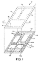
- FIG. 1 is an exploded perspective view showing the configuration of the electronic device of the present invention.
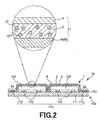
- FIG. 2 is a longitudinal cross-sectional view (a cross-sectional view taken along line AA in FIG. 1) showing the configuration of the sheet material according to the first embodiment (a state bonded to the electronic substrate).
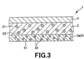
- FIG. 3 is an enlarged cross-sectional view illustrating the configuration of the sheet material according to the second embodiment (a state before being bonded to the electronic substrate).
- FIG. 4 is an enlarged cross-sectional view illustrating a configuration of the sheet material according to the third embodiment (a state before being bonded to the electronic substrate).
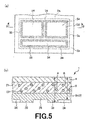
- FIGS. 5A and 5B are diagrams (a) is a plan view showing the vicinity of the insulating layer, and FIG.
- FIG. 5B is a plan view showing the structure of the sheet material according to the fourth embodiment (before being bonded to the electronic substrate).
- FIG. 3 is a diagram showing a central portion in a cross section taken along line BB.
- FIG. 6 is a plan view showing another configuration of the sheet material according to the fourth embodiment (a state before being bonded to the electronic substrate).
- 7A and 7B are diagrams showing the configuration of the sheet material according to the fifth embodiment (the state before being bonded to the electronic substrate), where FIG. 7A is a plan view and FIG. 7B is a cross-sectional view taken along line CC in FIG. The figure which shows the center part and edge part in FIG.
- FIG. 8 is a plan view illustrating another configuration of the sheet material according to the fifth embodiment (a state before bonding to the electronic substrate).
- FIG. 9 is a longitudinal sectional view showing the configuration of the end of the electronic device of the sixth embodiment.
- FIG. 10 is an enlarged cross-sectional view illustrating a configuration of the sheet material according to
- FIG. 1 is an exploded perspective view showing the configuration of the electronic device of the present invention.
- the upper side in FIG. 1 is “upper” and the lower side is “lower”.
- the electronic element 10 of the present invention includes an electronic substrate 100 and a sheet material 1 bonded (laminated) to the electronic substrate 100.
- the electronic substrate 100 First, prior to the description of the sheet material 1, the electronic substrate 100 will be described.
- the electronic board 100 include a flexible printed board, a rigid printed board, and a rigid flexible board.
- the electronic substrate 100 includes a wiring substrate 110 having a mounting surface 101 and a plurality of semiconductor chips (electronic components) 120 mounted on the mounting surface 101 of the wiring substrate 110.
- the semiconductor chip 120 include a CPU chip, a memory chip, a power supply chip, and a sound source chip.
- the wiring substrate 110 includes a substrate 111, a wiring 112 formed on the substrate 111, and a ground wiring (ground portion) 113.
- One end of the wiring 112 is connected to the power supply, and the other end is connected to a terminal of the semiconductor chip 120.
- the ground wiring 113 is formed in a frame shape so as to avoid the wiring 112 and is grounded.
- the mounting surface 101 is partitioned into first to third mounting regions 101a to 101c by the ground wiring 113 as shown in FIG.
- a predetermined semiconductor chip 120 is mounted on each of the mounting regions 101a to 101c.
- the sheet material 1 is bonded to the electronic substrate 100 having such a configuration. Hereinafter, the sheet material 1 will be described.
- FIG. 2 is a longitudinal cross-sectional view (a cross-sectional view taken along line AA in FIG. 1) showing the configuration of the sheet material according to the first embodiment (a state bonded to the electronic substrate).
- the upper side in FIG. 2 is “upper” and the lower side is “lower”.
- the sheet material 1 includes a sheet-like base material 2 having conductivity, an insulating layer 3 provided on the lower surface (one surface) of the base material 2, and the upper surface (the other side) of the base material 2. And a hard coat layer 4 provided on the surface.
- the sheet material 1 is bonded to the electronic substrate 100 with the insulating layer 3 facing the electronic substrate 100.
- the substrate 2 only needs to have conductivity, and may be formed of a metal film.
- the resin film including the solidified or cured product of the resin 21 and the conductive particles 22 is used. It is preferable that it is comprised.
- the substrate 2 may be a combination of these metal films and resin films, or may be a combination of two or more different resin films. The configuration of such a combination will be described in a later embodiment.
- this metal film can be formed using the thing similar to the metal quoted in the electroconductive particle 22.
- the conductivity of the base material 2 can be set to isotropic conductivity or anisotropic conductivity according to the type (purpose) of the wiring board 110.
- the isotropic conductivity means that the base material 2 has conductivity in the thickness direction and the surface direction
- the anisotropic conductivity means that the base material 2 has conductivity only in the thickness direction. Say that.
- Examples of the resin 21 include thermoplastic resins, curable resins, and the like, and one or more of these can be used in combination.
- Examples of the curable resin include a thermosetting resin, a photocurable resin, an anaerobic curable resin, a reaction curable resin, and the like. At least one of the thermosetting resin and the photocurable resin is used. preferable. The effect obtained by using at least one of a curable resin, in particular, a thermosetting resin and a photocurable resin, as the resin 21 will be described later.
- thermoplastic resin examples include polyolefin resins, vinyl resins, styrene / acrylic resins, diene resins, terpene resins, petroleum resins, cellulose resins, polyamide resins, polyurethane resins, polyester resins, Examples thereof include polycarbonate resins and fluorine resins.
- the thermosetting resin may be a resin having at least one functional group in one molecule that can be used for a crosslinking reaction by heating.
- this functional group for example, hydroxyl group, phenolic hydroxyl group, methoxymethyl group, carboxyl group, amino group, epoxy group, oxetanyl group, oxazoline group, oxazine group, aziridine group, thiol group, isocyanate group, blocked isocyanate group, Examples thereof include a blocked carboxyl group and a silanol group.
- thermosetting resins include, for example, acrylic resins, maleic resins, polybutadiene resins, polyester resins, polyurethane resins, urea resins, epoxy resins, oxetane resins, phenoxy resins, Polyimide resin, polyamide resin, polyamideimide resin, phenol resin, cresol resin, melamine resin, alkyd resin, amino resin, polylactic acid resin, oxazoline resin, benzoxazine resin, silicone resin And fluorine-based resins.
- acrylic resins acrylic resins, maleic resins, polybutadiene resins, polyester resins, polyurethane resins, urea resins, epoxy resins, oxetane resins, phenoxy resins, Polyimide resin, polyamide resin, polyamideimide resin, phenol resin, cresol resin, melamine resin, alkyd resin, amino resin, polylactic acid resin, oxazoline resin, benzoxazine resin, silicone resin And fluorine-based resin
- the base material 2 is made of a curing agent such as a resin or a low-molecular compound that reacts with the functional group to form a chemical crosslink in addition to the thermosetting resin. It is preferable to include.
- a curing agent is not particularly limited.
- a curing agent capable of causing a curing reaction to proceed at a relatively high temperature such as a phenolic curing agent such as a phenol novolac resin, or an amine curing agent such as dicyandiamide or aromatic diamine.
- the curing agent examples include an curing agent, an isocyanate curing agent, an epoxy curing agent, an aziridine curing agent, and a metal chelate curing agent that can cause the curing reaction to proceed at a relatively low temperature (for example, 120 ° C. or less).
- the photocurable resin may be a resin having one or more unsaturated bonds in one molecule that cause a crosslinking reaction by light.
- the photocurable resin include, for example, acrylic resins, maleic resins, polybutadiene resins, polyester resins, polyurethane resins, epoxy resins, oxetane resins, phenoxy resins, polyimide resins, polyamides. Resin, phenol resin, alkyd resin, amino resin, polylactic acid resin, oxazoline resin, benzoxazine resin, silicone resin, fluorine resin and the like.
- the conductive particles 22 are dispersed in such a solidified or cured product of the resin 21.
- the base material 2 sheet material 1
- the conductive particles 22 include metal particles, carbon particles, conductive resin particles, and the like, and one or more of these can be used in combination.
- the metal constituting the metal particles examples include gold, platinum, silver, copper, nickel, aluminum, iron or alloys thereof, ITO, ATO, etc., but copper is preferable from the viewpoint of price and conductivity.
- the metal particle may be a particle including a core made of metal and a coating layer that covers the core and is made of metal. Examples of such metal particles include silver-coated copper particles obtained by coating a nucleus composed of copper with a coating layer composed of silver.
- examples of carbon constituting the carbon particles include acetylene black, ketjen black, furnace black, carbon nanotube, carbon nanofiber, graphite, fullerene, graphene and the like.
- examples of the conductive resin constituting the conductive resin particles include poly (3,4-ethylenedioxythiophene), polyacetylene, polythiophene, and the like.
- the average particle diameter of the conductive particles 22 is preferably about 1 to 100 ⁇ m, more preferably about 3 to 75 ⁇ m, and further preferably about 5 to 50 ⁇ m.
- the filling rate of the conductive particles 22 in the substrate 2 can be improved. For this reason, the electromagnetic wave shielding effect of the base material 2 (sheet material 1) can be improved more.
- the resin composition is prepared by mixing with the resin 21, the fluidity is improved, so that the moldability to the substrate 2 is improved.
- the shape of the conductive particles 22 may be any shape such as a spherical shape, a needle shape, a flake shape, or a dendritic shape.
- the average particle diameter of the conductive particles 22 can be obtained by measurement using a general laser diffraction method, scattering method, or the like, and the average value of diameters assuming a circle equal to the projected area of the fine particle aggregate. Can be the average particle size.
- the content of the conductive particles 22 in the substrate 2 is not particularly limited, but is preferably 100 to 1500 parts by weight, more preferably 100 to 1000 parts by weight with respect to 100 parts by weight of the resin 21. .
- the base material 2 can be provided with necessary and sufficient conductivity regardless of the type of the conductive particles 22.
- the electromagnetic wave shielding effect can be sufficiently enhanced.
- liquidity of the resin composition containing the resin 21 and the electroconductive particle 22 increases, and it is preferable also from becoming easy to form the base material 2.
- the average thickness of the substrate 2 is not particularly limited, but is preferably about 2 to 500 ⁇ m, and more preferably about 5 to 100 ⁇ m. By making the average thickness of the base material 2 within the above range, it is possible to reduce the thickness of the base material 2 while preventing the mechanical strength of the base material 2 from being lowered.
- the base material 2 is, for example, a colorant (pigment, dye), a flame retardant, a filler (inorganic additive), a lubricant, an antiblocking agent, a metal deactivator, a thickener, a dispersant, a silane coupling.
- a colorant pigment, dye
- a filler inorganic additive
- a lubricant for example, a lubricant
- an antiblocking agent e.g., stannous, sodium sulfate
- a metal deactivator e.g., sodium bicarbonate
- a thickener e.g., sodium bicarbonate
- dispersant e.g., sodium silane coupling
- silane coupling e.g., sodium silane coupling
- Agents rust inhibitors, copper damage inhibitors, reducing agents, antioxidants, tackifier resins, plasticizers, ultraviolet absorbers, antifoaming agents, leveling regulators, and the like.
- Examples of the colorant include organic pigments, carbon black, ultramarine blue, petals, zinc white, titanium oxide, graphite and the like.
- Examples of the flame retardant include a halogen-containing flame retardant, a phosphorus-containing flame retardant, a nitrogen-containing flame retardant, and an inorganic flame retardant.
- Examples of the filler include glass fiber, silica, talc, and ceramic.
- examples of the lubricant include fatty acid esters, hydrocarbon resins, paraffin, higher fatty acids, fatty acid amides, aliphatic alcohols, metal soaps, modified silicones, and the like.
- examples of the anti-blocking agent include calcium carbonate, silica, polymethylsilsesquiosan, aluminum silicate salt and the like.
- the insulating layer 3 is provided on the lower surface (surface on the electronic substrate 100 side) of the base material 2.
- the first insulating layer 3 a corresponding to the first mounting region 100 a of the mounting surface 101 (wiring substrate 110) and the second mounting are formed on the lower surface of the base material 2.
- a second insulating layer 3b corresponding to the region 100b and a third insulating layer 3c corresponding to the third mounting region 100c are provided.
- Each of the first to third insulating layers 3a to 3c (hereinafter collectively referred to simply as “insulating layer 3”) is smaller than the substrate 2 in plan view, and is a sheet.
- the size includes one or more semiconductor chips 120.
- a strip-shaped exposed region 2a exposed from the first to third insulating layers 3a to 3c is formed on the lower surface of the substrate 2. Therefore, the exposed region 2 a has a shape corresponding to the shape of the ground wiring 113 of the wiring board 110.
- the exposed region 2a of the base material 2 constitutes a connecting portion (joining portion) that connects (joins) the sheet material 1 to the wiring board 110.
- the cured product is obtained by curing the curable resin after bringing the exposed region 2 a of the base material 2 into contact with the ground wiring 113 of the wiring substrate 110.
- the sheet material 1 and the electronic substrate 100 can be joined (fixed) at the contact portion.
- the insulating layer 3 only needs to have sufficient insulating properties, and can be formed using a hard resin or a curable resin (particularly a thermosetting resin).
- a hard resin include acrylic, polyurethane, polyurethane urea, epoxy, epoxy ester, polyester, polycarbonate, polyphenylene sulfide, and the like, and one or more of these can be used in combination.
- the curable resin the same curable resin as mentioned in the resin 21 can be used.
- the insulating layer 3 may contain the same curing agent as described in the base material 2.
- the degree of curing (fully cured or semi-cured state) of the insulating layer 3 in the sheet material 1 before lamination (before use) on the electronic substrate 100 the degree of fluidity (solid state or gel state), and adhesiveness.
- the degree of curing can be controlled.
- the insulating layer 3 includes, for example, a colorant (pigment, dye), a flame retardant, a filler (inorganic additive), a lubricant, an antiblocking agent, a metal deactivator, a thickener, a dispersant, a silane coupling.
- a colorant pigment, dye
- a flame retardant for example, a flame retardant, a filler (inorganic additive), a lubricant, an antiblocking agent, a metal deactivator, a thickener, a dispersant, a silane coupling.
- a colorant pigment, dye
- a filler inorganic additive
- the average thickness of the insulating layer 3 is not particularly limited, but is preferably about 50 to 200 when the average thickness of the substrate 2 is 100, more preferably about 75 to 150. preferable. Specifically, the average thickness of the insulating layer 3 is preferably about 1 to 1000 ⁇ m, and more preferably about 3 to 200 ⁇ m. Thereby, the insulating layer 3 can impart excellent followability to the surface of the electronic substrate 100 to the insulating layer 3 (sheet material 1) while maintaining sufficient insulation.
- the insulating layer 3 and the surface of the semiconductor chip 120 are in close contact with each other.
- the adhesion of the insulating layer 3 to the surface of the semiconductor chip 120 can be further improved.
- this operation may be performed under reduced pressure or vacuum when the sheet material 1 is bonded to the electronic substrate 100.
- the lower surface of the insulating layer 3 may be a smooth surface or a rough surface. If the lower surface of the insulating layer 3 (surface on the electronic substrate 100 side) is a smooth surface, the contact area between the insulating layer 3 and the surface of the semiconductor chip 120 can be increased, and the heat dissipation effect of the sheet material 1 can be improved. Can do. On the other hand, when the lower surface of the insulating layer 3 is formed of a rough surface, the contact area between the insulating layer 3 and the surface of the semiconductor chip 120 can be slightly reduced, and when the electronic substrate 100 is recycled, the insulating layer 3 ( The sheet material 1) can be removed more easily.
- a hard coat layer (protective layer) 4 having a function of protecting the base material 2 is provided on the upper surface of the base material 2 (the surface opposite to the electronic substrate 100). Thereby, damage to substrate 2 can be prevented suitably.
- Such a hard coat layer 4 includes, for example, a bifunctional or monofunctional or monofunctional monomer having an ⁇ , ⁇ -unsaturated double bond, a vinyl monomer, an allyl monomer, a monofunctional (meth) acrylate monomer, a polyfunctional monomer, It is preferably composed of a polymer (cured product) of a radical polymerization monomer such as a functional (meth) acrylate monomer.
- a radical polymerization monomer such as a functional (meth) acrylate monomer.
- the bifunctional or higher monomer having an ⁇ , ⁇ -unsaturated double bond is, for example, a relatively low molecular weight monomer having a molecular weight of less than 1000 (so-called narrowly-defined monomer), for example, having a weight average molecular weight of 1000 or more. It may be a relatively high molecular weight oligomer or prepolymer of less than 10,000.
- examples of the oligomer having an ⁇ , ⁇ -unsaturated double bond include polyester (meth) acrylate, polyurethane (meth) acrylate, epoxy (meth) acrylate, (meth) acrylated maleic acid-modified polybutadiene, and the like. It is done.
- vinyl monomer examples include styrene, ⁇ -methylstyrene, divinylbenzene, N-vinylpyrrolidone, vinyl acetate, N-vinylformaldehyde, N-vinylcaprolactam, alkyl vinyl ether and the like.
- allyl monomers include trimethacryl isocyanurate and triallyl cyanurate.
- Examples of monofunctional (meth) acrylate monomers include 2- (meth) acryloyloxyethyl phthalate, 2- (meth) acryloyloxyethyl-2-hydroxyethyl phthalate, and 2- (meth) acryloyloxyethyl hexahydro.
- polyfunctional (meth) acrylate monomer examples include 1,3-butylene glycol di (meth) acrylate, 1,4-butanediol di (meth) acrylate, 1,6-hexanediol di (meth) acrylate, 1, 9-nonanediol di (meth) acrylate, bisphenol A di (meth) acrylate, bisphenol F di (meth) acrylate, diethylene glycol di (meth) acrylate, hexahydrophthalic acid di (meth) acrylate, hydroxypivalate neopentyl glycol di (Meth) acrylate, neopentyl glycol di (meth) acrylate, hydroxypivalate ester neopentyl glycol di (meth) acrylate, pentaerythritol di (meth) acrylate, di (meth) acrylate phthalate Polyethylene glycol di (meth) acrylate, poly(
- the hard coat layer 4 is made of, for example, a polyester resin such as polyethylene terephthalate (PET) or polybutylene terephthalate (PBT), an acrylic resin such as polymethyl methacrylate, polyethylene, polypropylene, ethylene-vinyl acetate copolymer. It can also be composed of a thermoplastic resin such as a polyolefin-based resin such as a coalescence.
- a polyester resin such as polyethylene terephthalate (PET) or polybutylene terephthalate (PBT)
- an acrylic resin such as polymethyl methacrylate
- polyethylene polypropylene
- ethylene-vinyl acetate copolymer ethylene-vinyl acetate copolymer
- thermoplastic resin such as a polyolefin-based resin such as a coalescence.
- the hard coat layer 4 is, for example, a colorant (pigment, dye), a flame retardant, a filler (inorganic additive), a lubricant, an antiblocking agent, a metal deactivator, a thickener, a dispersant, a silane cup.
- a ring agent, a rust preventive agent, a copper damage inhibitor, a reducing agent, an antioxidant, a tackifier resin, a plasticizer, an ultraviolet absorber, an antifoaming agent, a leveling regulator, and the like may be contained.
- the average thickness of the hard coat layer 4 is not particularly limited, but is preferably about 0.1 to 10 ⁇ m, preferably 0.5 to 5 ⁇ m. More preferred is the degree.
- the average thickness of the hard coat layer 4 is preferably about 1 to 50 ⁇ m, and more preferably about 5 to 30 ⁇ m.
- the protective layer is not limited to the hard coat layer 4 and may be a cushion layer, a print layer, or the like that absorbs external stress or impact, and is a laminate in which these layers are combined. Also good.
- the sheet material 1 as described above can be manufactured, for example, as follows.
- the resin composition for a hard coat layer on a release sheet After applying the resin composition for a hard coat layer on a release sheet, it is cured or solidified. Thereby, the hard coat layer 4 is obtained.
- the base material resin composition is applied onto the hard coat layer 4, it is semi-cured, cured or solidified. Thereby, the base material 2 is obtained. In this state, the base material 2 may or may not have adhesiveness.
- the insulating layer resin composition is coated on the substrate 2, it is semi-cured, cured or solidified. Thereby, the insulating layer 3 is obtained. In this state, the insulating layer 3 may or may not have adhesiveness.
- Examples of methods for applying each resin composition include gravure coating, kiss coating, die coating, lip coating, comma coating, blade coating, roll coating, knife coating, spray coating, and bar coating.
- a spout coat method, a dip coat method, or the like can be used.
- seat material 1 may be made to join these layers mutually.
- a heat conduction layer for example, a water vapor barrier layer, an oxygen barrier layer, a low dielectric constant layer, a high dielectric constant layer,
- a heat conduction layer for example, a heat conduction layer, a water vapor barrier layer, an oxygen barrier layer, a low dielectric constant layer, a high dielectric constant layer,
- a heat conduction layer for example, a heat conduction layer, a water vapor barrier layer, an oxygen barrier layer, a low dielectric constant layer, a high dielectric constant layer,
- a low dielectric loss tangent layer for example, a heat conduction layer, a water vapor barrier layer, an oxygen barrier layer, a low dielectric constant layer, a high dielectric constant layer,
- a heat resistant layer for example, a heat conduction layer, a water vapor barrier layer, an oxygen barrier layer, a low dielectric constant layer, a high dielectric constant layer,
- a heat conduction layer for example, a water vapor barrier layer, an oxygen barrier layer,
- Such a sheet material 1 is bonded to the electronic substrate 100 as follows.
- the sheet material 1 is laminated on the electronic substrate 100 with the insulating layer 3 facing the electronic substrate 100 side.
- the insulating layer 3 is in close contact with the surface of the semiconductor chip 120, and the exposed region 2a of the base material 2 is in contact with the ground wiring 113.
- the sheet material 1 is fixed (bonded) to the electronic substrate 100.
- the electronic element 10 is obtained.
- the degree of adhesion of the insulating layer 3 to the surface of the semiconductor chip 120 is increased by performing thermocompression bonding under reduced pressure or vacuum. As a result, not only the electromagnetic wave shielding effect by the sheet material 1 but also a good heat dissipation effect is exhibited.
- the thermosetting resin is cured by the heating and pressing, and the exposed region 2a of the substrate 2 is grounded by the cured product.
- the wiring 113 is firmly joined.
- the mechanical strength of the base material 2 (sheet material 1) itself is also improved by the curing of the thermosetting resin.
- the base material 2 contains a photocurable resin, light (active radiation) is irradiated to the exposed area
- a brazing material (solder) is provided on the ground wiring 113 prior to the thermocompression bonding, so that the exposed region 2a of the base material 2 becomes the ground wiring 113. It is firmly joined through the brazing material.
- Such an electronic element 10 is easy to remove heat from the semiconductor chip 120, is thin, and has high reliability.
- a mobile phone such as a smartphone, a personal computer, a tablet terminal, LED lighting, It can be used for in-vehicle parts such as organic EL lighting, liquid crystal television, organic EL television, digital camera, digital video camera and automobile.
- FIG. 3 is an enlarged cross-sectional view showing the configuration of the sheet material according to the second embodiment (a state before being bonded to the electronic substrate).
- the second embodiment will be described, the description will focus on the differences from the first embodiment, and the description of the same matters will be omitted.
- the upper side in FIG. 3 is “upper” and the lower side is “lower”.
- the sheet material 1 of the second embodiment is the same as the first embodiment except for the configuration of the insulating layer 3 (first to third insulating layers 3a to 3c). That is, as shown in FIG. 3, the insulating layer 3 of the second embodiment includes a resin 31 and thermally conductive particles 32 dispersed in the resin 31 and having a thermal conductivity higher than that of the resin 31. Including. By including the heat conductive particles 32 in the insulating layer 3, the heat conductivity of the sheet material 1 is improved, and the heat dissipation effect by the sheet material 1 is further increased.
- Examples of the constituent material of the heat conductive particles 32 include metal oxides such as calcium oxide, magnesium oxide, and aluminum oxide, metal hydroxides such as aluminum hydroxide and magnesium hydroxide, aluminum nitride, and boron nitride.
- Metal carbonates such as calcium carbonate, magnesium carbonate, metal silicates such as calcium silicate, crystalline silica, amorphous silica, silicon compounds such as silicon carbide, etc. 1 type or 2 types or more can be used in combination.
- the constituent material of the thermally conductive particles 32 is preferably at least one of aluminum oxide, aluminum nitride, and boron nitride, and aluminum oxide is more preferable because of high heat resistance and insulation reliability. Further, spherical aluminum oxide is excellent in that it can be closely packed in the insulating layer 3, and is particularly preferable in that it can prevent the elastic modulus of the insulating layer 3 from being unnecessarily increased even when the filling amount is increased.
- the heat conductive particles 32 may include a plurality of types of particles.
- the average particle diameter of the heat conductive particles 32 is not particularly limited, but is preferably about 0.1 to 250 ⁇ m, and more preferably about 0.5 to 100 ⁇ m. Since the heat conductive particles 32 having such an average particle diameter are easily dispersed uniformly in the insulating layer 3, the heat conductivity of the insulating layer 3 can be further increased.
- the shape of the heat conductive particles 32 may be any shape such as a spherical shape, a needle shape, a flake shape, or a dendritic shape.
- the average particle diameter of the heat conductive particles 32 can be obtained by measurement using a general laser diffraction method, scattering method, or the like, and the average diameter when a circle equal to the projected area of the fine particle aggregate is assumed. The value can be the average particle size.
- the content of the heat conductive particles 32 in the insulating layer 3 is not particularly limited, but is preferably about 25 to 95% by weight, and more preferably about 35 to 85% by weight. By making the content of the heat conductive particles 32 in the insulating layer 3 within the above range, the thermal conductivity of the insulating layer 3 is sufficiently improved while preventing the mechanical strength of the insulating layer 3 from being lowered. Can do.
- the same resin that can be used for the insulating layer 3 in the first embodiment can be used.
- the insulating layer 3 may contain the same curing agent as described in the first embodiment.
- FIG. 4 is an enlarged cross-sectional view showing a configuration of the sheet material according to the third embodiment (a state before being bonded to the electronic substrate).
- the third embodiment will be described. The description will focus on the differences from the first embodiment, and the description of the same matters will be omitted. In the following, for convenience of explanation, the upper side in FIG. 4 is “upper” and the lower side is “lower”.
- the sheet material 1 of the third embodiment is the same as the first embodiment except that the configuration of the base material 2 is different. That is, as shown in FIGS. 4A and 4B, the base material 2 of the third embodiment includes a main body portion 20 including a resin 21 and conductive particles 22, and the insulating layer 3 side of the main body portion 20. And a metal film 23 provided in contact with the main body 20. When the base material 2 includes the metal film 23, the electromagnetic wave shielding effect and the heat dissipation effect of the base material 2 (sheet material 1) are more suitably exhibited.
- the metal film 23 is formed by attaching (joining) a metal foil formed of the metal mentioned in the conductive particle 22 to the main body 20, or the metal oxide (eg, ITO, ATO) mentioned in the conductive particle 22.
- a method of forming a deposited film or a sputtering film on the main body 20 by vapor deposition or sputtering, a method of forming a printed film on the main body 20 by printing a conductive paste (for example, silver paste), etc. Can be obtained.
- various copper foil is preferable from the surface of electroconductivity and cost, and rolled copper foil or electrolytic copper foil is more preferable.
- the average thickness of the metal film 23 is not particularly limited, but is preferably about 0.004 to 2500% of the average thickness of the base material 2, and preferably about 0.025 to 75%. By making the average thickness of the metal film 23 within the above range, the electromagnetic wave shielding effect and the heat radiation effect of the base material 2 are sufficiently exhibited while preventing the flexibility of the base material 2 (sheet material 1) from being lowered. Is done.
- the specific average thickness of the metal film 23 is preferably as follows.
- the average thickness is preferably about 50 to 300 nm, and more preferably about 75 to 200 nm.
- the average thickness is preferably about 20 to 80 nm, and more preferably about 25 to 70 nm.
- the average thickness is preferably about 0.01 to 20 ⁇ m, and more preferably about 0.1 to 15 ⁇ m.
- the metal film 23 may be substantially the same size as the insulating layer 3 in a plan view, and as shown in FIG. The sizes may be approximately equal.
- the sheet material 1 can be firmly bonded to the electronic substrate 100 using the main body portion 20 of the exposed region 2 a.
- the metal film 23 in the exposed region 2a can be metal-bonded to the ground wiring 113 of the wiring board 110 by, for example, laser irradiation. For this reason, extremely high joining between the sheet material 1 and the electronic substrate 100 is possible.
- such a metal film 23 may have a mesh shape or a shape having a plurality of through holes formed by punching. By making such a shape, water vapor permeability can be imparted to the metal film 23.
- the metal film 23 may be provided so as to be in contact with the main body 20, and may be provided on the hard coat layer 4 side instead of the insulating layer 3 side. These may be provided at any arbitrary position, or a combination thereof.
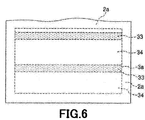
- FIGS. 5A and 5B are diagrams showing the configuration of the sheet material according to the fourth embodiment (the state before being bonded to the electronic substrate), where FIG. 5A is a plan view showing the vicinity of the insulating layer 3a, and FIG. FIG. 6 is a plan view showing another configuration of the sheet material of the fourth embodiment (a state before being bonded to the electronic substrate).
- the fourth embodiment will be described. The description will focus on the differences from the first embodiment, and the description of the same matters will be omitted. In the following, for convenience of explanation, the upper side in FIG. 5B and FIG. 6 is “upper” and the lower side is “lower”.
- the thickness of the insulating layer 3 is non-uniform in a state before the sheet material 1 is bonded to the electronic substrate 100 (a state before use of the sheet material 1).
- the average thickness of the region 33 is larger than the average thickness of the second region 34 other than the first region 33.
- the first region 33 has a rectangular frame shape in plan view corresponding to the outer peripheral shape of the semiconductor chip 120.
- the average thickness of the first region 33 of the sheet material 1 is A [ ⁇ m]
- the average thickness of the second region 34 is B [ ⁇ m].
- a / B is preferably about 1.05 to 3, more preferably about 1.05 to 1.4, and still more preferably about 1.1 to 1.25.
- Such an insulating layer 3 is formed on the first region 33 of the insulating layer 3 after forming a portion having a uniform thickness on the substrate 2 side of the insulating layer 3 by the method described in the first embodiment. It can be obtained by stacking and forming quadrangular frame shapes.
- the first region 33 is not limited to the region shown in FIG. 5A, and may be a region where the sheet material 1 is particularly easily broken.
- the first region 33 is provided as shown in FIG. 6. Further, it can be a linear region continuously contacting along the edge of the two semiconductor chips 120.
- the extent to which the sheet material 1 is stretched is increased at the locations where the semiconductor chips 120 are densely arranged. For this reason, a linear region straddling the two semiconductor chips 120 as shown in FIG. 6 is defined as the first region 33, and the thickness of the insulating layer 3 (sheet material 1) in the first region 33 is increased. Thus, breakage of the sheet material 1 can be sufficiently prevented.
- the sheet material 1 in the state before the sheet material 1 is bonded to the electronic substrate 100, the sheet material 1 only needs to have an average thickness of the first region 33 larger than an average thickness of the second region 34.
- the base material 2 instead of forming the insulating layer 3 to be partially thick, the base material 2 is partially thick, and the hard coat layer 4 is partially thick. Or a combination thereof.
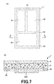
- FIG. 7A and 7B are diagrams showing the configuration of the sheet material according to the fifth embodiment (the state before being bonded to the electronic substrate), where FIG. 7A is a plan view, and FIG. FIG. 8 is a plan view showing another configuration of the sheet material of the fifth embodiment (a state before being joined to the electronic substrate).
- FIG. 7B the upper side in FIG. 7B is referred to as “upper” and the lower side is referred to as “lower”.
- the sheet material 1 of the fifth embodiment has an insulating portion 35 provided separately from the insulating layer 3 along the edge portion of the lower surface of the base material 2, and otherwise the same as in the first embodiment. It is. That is, as shown in FIGS. 7A and 7B, the insulating portion 35 is formed along the edge of the lower surface of the substrate 2 so as to surround the first to third insulating layers (3a to 3c). It is formed in a rectangular frame shape. With this configuration, it is possible to prevent the base material 2 and the mounting surface 101 of the wiring board 110 from directly contacting each other at the edge of the sheet material 1 in a state where the sheet material 1 is bonded (laminated) to the electronic substrate 100. it can. For this reason, the unintentional short circuit between the base material 2 and the wiring board 110 can be prevented, and the highly reliable electronic device 10 can be obtained.
- the portion of the sheet material 1 on which the insulating portion 35 is formed is gripped, which becomes a trigger for the peeling operation.
- the peeling operation can be easily performed. That is, the portion of the sheet material 1 where the insulating portion 35 is provided constitutes a grip portion that is gripped when the sheet material 1 is separated from the electronic substrate 100 on which the sheet material 1 is laminated.
- the insulating portion 35 is formed in a frame shape along the edge portion of the base material 2, so that the peeling operation is performed from any part of the entire circumference of the sheet material 1. Can start.
- the constituent material of the insulating part 35 is preferably the same as the hard resin mentioned in the insulating layer 3 of the first embodiment.
- the insulating portion 35 By configuring the insulating portion 35 with a hard resin, it is possible to prevent the insulating portion 35 from being bonded to the mounting surface 101 of the wiring substrate 110. For this reason, when the sheet material 1 is peeled from the electronic substrate 100, the portion of the sheet material 1 where the insulating portion 35 is formed can be gripped more easily and reliably.
- the average thickness of the insulating portion 35 is preferably set smaller than the average thickness of the insulating layer 3. Thereby, the insulating part 35 can be made into the state which contacted the mounting surface 101 of the wiring board 110 lightly. For this reason, when the sheet material 1 is peeled off from the electronic substrate 100, the portion of the sheet material 1 on which the insulating portion 35 is formed becomes easier to grip.
- the insulating portion 35 can be formed by, for example, the same method as the insulating layer 3, and may be formed in the same process as the insulating layer 3, or may be formed in a process different from the insulating layer 3. It may be.
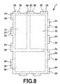
- the base member 2 is provided with a plurality of ear portions 24 formed at intervals along the edge portion, and an insulating portion 35 is provided on the lower surface of each ear portion 24. May be. That is, a plurality of insulating portions 35 may be provided along the edge portion of the base material 2 at intervals.
- the electronic substrate 100 can be accommodated in the casing of the electronic device with the ear portion 24 folded. For this reason, it can prevent that the ear
- ear 24 (insulating part 35) may be provided from the viewpoint of starting the peeling operation when the electronic substrate 100 is recycled.
- FIG. 9 is a longitudinal sectional view showing the configuration of the end of the electronic device of the sixth embodiment.
- the sixth embodiment will be described, the description will focus on differences from the first embodiment, and the description of the same matters will be omitted.
- the upper side in FIG. 9 is “upper” and the lower side is “lower”.
- the sheet material 1 of the sixth embodiment includes a base material 2 made of a metal film and an insulating layer 3 provided on the lower surface (one surface) of the base material 2. It has a two-layer structure.
- a plurality of conductive pins 114 are provided on the upper surface of the ground wiring 113 at predetermined intervals along the longitudinal direction of the ground wiring 113. Each conductive pin 114 is arranged with the needle tip (top) facing upward.
- the ground portion is configured by the ground wiring 113 and the conductive pin 114.
- the conductive pin 114 may be formed integrally with the ground wiring 113.
- the ground wiring 113 may be omitted and the conductive pin 114 may be directly grounded.
- Such conductive pins 114 can be formed using the same metals as those mentioned in the conductive particles 22 of the first embodiment.
- the sheet material 1 may have the same configuration as the sheet material 1 of the first to fifth embodiments.
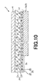
- FIG. 10 is an enlarged cross-sectional view illustrating the configuration of the sheet material according to the seventh embodiment (a state before being bonded to the electronic substrate).
- the seventh embodiment will be described, the description will focus on the differences from the first embodiment, and description of similar matters will be omitted.
- the upper side in FIG. 10 is “upper” and the lower side is “lower”.
- the sheet material 1 of the seventh embodiment is the same as the first embodiment except that the configuration of the base material 2 is different. That is, as shown in FIG. 10, the base material 2 of the seventh embodiment includes a lower layer (first portion) 2 ⁇ / b> X provided in contact with the insulating layer 3, and the lower layer 2 ⁇ / b> X (on the opposite side to the insulating layer 3). ) Provided on the upper layer (second portion) 2Y.
- the lower layer 2X includes a resin (first resin) 25 and conductive particles (first conductive particles) 26 dispersed in the resin 25, and the upper layer 2Y includes a resin (second resin) 21. And conductive particles (second conductive particles) 22 dispersed in the resin 21. Further, the content in the upper layer 2Y of the conductive particles 22 is set to be larger than the content in the lower layer 2X of the conductive particles 25.
- the upper layer 2Y can exhibit high electromagnetic shielding properties, and the lower layer 2X can be provided with adhesiveness depending on the type of the resin 25 and the like. Therefore, when the sheet material 1 of this embodiment is laminated on the electronic substrate 100, the exposed region 2a of the sheet material 1 (base material 2) is attached to the ground wiring 113 by using the adhesiveness of the lower layer 2X. And can be fixed.
- thermocompression bonding the sheet material 1 to the electronic substrate 100 is omitted, that is, the sheet material 1 is attached to the electronic substrate 100 manually by the operator. Can do. Therefore, the production efficiency of the electronic substrate 100 can be improved. Moreover, since the operation of thermocompression bonding can be omitted, the semiconductor chip 120 can be prevented from being deteriorated by heating at this time, and the electronic element 10 with higher reliability can be obtained.
- the resin 25 is preferably a resin (including rubber) having a glass transition temperature of 0 ° C. or lower, and a resin (including rubber) having a glass transition temperature of ⁇ 10 ° C. or lower from the viewpoint of imparting higher adhesion to the lower layer 2X. More preferably, a resin (including rubber) having a glass transition temperature of ⁇ 20 ° C. or lower is more preferable. Specific examples of such resins (including rubber) include various resins such as acrylic resins and urethane resins, various rubbers such as natural rubber and synthetic rubber, and various thermoplastics such as styrene block copolymers. An elastomer etc. are mentioned. Further, the lower layer 2X may contain the same curing agent as described in the first embodiment.
- the lower layer 2X may have either isotropic conductivity or anisotropic conductivity, but preferably has anisotropic conductivity. Thereby, the electric current which flows into upper layer 2Y can be smoothly transmitted by ground wiring 113 via lower layer 2X, and the electromagnetic wave shielding effect of substrate 2 (sheet material 1) is more suitably exhibited.
- the conductive particles 26 dispersed in the resin 25 particles having the same kind and average particle diameter as the conductive particles 22 described in the first embodiment can be used.
- the shape of the conductive particles 26 can also be the same shape as the conductive particles 22 described in the first embodiment, but is preferably dendritic or spherical.
- the dendritic or spherical conductive particles 26 can impart necessary and sufficient conductivity to the lower layer 2X even if the content in the lower layer 2X is relatively small.
- the adhesiveness of lower layer 2X can be improved more by making content in the lower layer 2X of the electroconductive particle 26 into a small quantity.
- the content of the conductive particles 26 in the lower layer 2X is preferably 1 to 100 parts by weight and more preferably 10 to 50 parts by weight with respect to 100 parts by weight of the resin 25.
- the resin 21 and the conductive particles 22 contained in the upper layer 2Y provided on the lower layer 2X can have the same configuration as described in the first embodiment.
- the upper layer 2Y may contain the same curing agent as described in the first embodiment.
- the upper layer 2Y may have either isotropic conductivity or anisotropic conductivity, but preferably has isotropic conductivity. Thereby, electromagnetic waves can be reliably captured by the upper layer 2Y, and the converted current can be quickly transmitted to the lower layer 2X.
- the lower layer 2X an anisotropic conductivity that is different from the isotropic conductivity of the upper layer 2Y
- the lower layer 2X and the upper layer 2Y can share different roles, and the base material 2 (sheet material 1 The electromagnetic wave shielding effect of) is more suitably exhibited.
- the shape of the conductive particles 22 is preferably different from the conductive particles 26 (particularly flakes).
- the upper layer 2 ⁇ / b> Y can contain a large amount of the conductive particles 22 and can have sufficient isotropic conductivity.
- the content in the upper layer 2Y of the conductive particles 22 is preferably 100 to 1500 parts by weight, more preferably 100 to 1000 parts by weight with respect to 100 parts by weight of the resin 21.
- the content in the upper layer 2Y of the conductive particles 22 is preferably 100 to 1500 parts by weight, more preferably 100 to 1000 parts by weight with respect to 100 parts by weight of the resin 21.
- the average thickness of the lower layer 2X is Tx [ ⁇ m] and the average thickness Ty [ ⁇ m] of the upper layer 2Y
- these ratios Ty / Tx are not particularly limited. It is preferably about 1 to 7.5, and more preferably about 2 to 5.
- the base material 2 that exhibits a higher electromagnetic shielding effect is obtained.
- the average thickness of the lower layer 2X is preferably about 0.5 to 150 ⁇ m, more preferably about 1.5 to 25 ⁇ m, and the average thickness of the upper layer 2Y is 1.5 to The thickness is preferably about 350 ⁇ m, more preferably about 3.5 to 75 ⁇ m.
- the upper layer 2Y may be composed of the same metal film as described in the third and sixth embodiments.
- the insulating layer 3 is provided on the lower surface (surface on the electronic substrate 100 side) of the base material 2.
- the insulating layer 3 can have the same configuration as described in the first or second embodiment, and also uses a resin composition containing the same resin 21 and curing agent as the upper layer 2Y. Can be formed.
- the insulating layer 3 may or may not have adhesiveness.
- the sheet material 1 of the present embodiment is preferably attached to the electronic substrate 100 manually by the operator.
- the insulating layer 3 has adhesiveness, the sheet material 1 can be easily positioned with respect to the electronic substrate 100 and the production efficiency of the electronic element 10 can be further improved. If the sheet material 1 is not sticky, the sheet material 1 is easily peeled off from the electronic substrate 100 even if it is once attached to the electronic substrate 100, and the position of the sheet material 1 relative to the electronic substrate 100 can be easily corrected.
- the sheet material 1 is fixed (laminated) to the electronic substrate 100 and then the layer is in this state. May be post-cured. Thereby, while being able to join the sheet material 1 to the electronic substrate 100, the mechanical strength of the sheet material 1 can also be improved.
- the lower layer 2X is made of a resin (including rubber) having a glass transition temperature of 0 ° C. or lower, a first curing agent capable of causing a curing reaction to proceed at a relatively low temperature as described in the first embodiment, If formed using a resin composition containing a second curing agent capable of causing a curing reaction to proceed at a higher temperature than the first curing agent and the conductive particles 26, the first material is used before the sheet material 1 is used.
- the lower layer 2X is made into a gel state (semi-solid state) by the action of the curing agent, and the lower layer 2X is made into a solid state by the action of the second curing agent by post-curing after the sheet material 1 is fixed (laminated) to the electronic substrate 100. It can be.
- the sheet material 1 is manufactured by forming the hard coat layer 4, the upper layer 2Y, the lower layer 2X, and the insulating layer 3 by coating the resin composition constituting each layer in the same manner as in the first embodiment. can do.
- the sheet material 1 since the lower layer 2X has adhesiveness, the sheet material 1 is prepared by previously preparing a laminated body in which the hard coat layer 4, the upper layer 2Y, and the lower layer 2X are laminated, and the insulating layer 3 created separately. You may manufacture by sticking to the lower layer 2X of a laminated body.
- one or more intermediate layers for any purpose may be provided between the lower layer 2X and the upper layer 2Y.
- an intermediate layer include an adhesion layer for improving adhesion between the lower layer 2X and the upper layer 2Y, the metal film 23 of the third embodiment, and the like.
- the adhesion layer is preferably composed of, for example, a mixture of a resin composition constituting the lower layer 2X and a resin composition constituting the upper layer 2Y.
- seat material can be substituted with the thing of the arbitrary structures which can exhibit the same function.
- arbitrary components may be added.
- the electronic element and the sheet material may be combined with any one of the first to seventh embodiments.
- the sheet material of each said embodiment has a hard-coat layer (protective layer), what is necessary is just to provide a hard-coat layer (protective layer) as needed, and can also be abbreviate
- the ground portion is not particularly limited as long as it can ground the base material of the sheet material (connected to the reference potential), and the form and shape thereof are not particularly limited.
- the sheet material may include a single insulating layer, and the single insulating layer may cover all electronic components, or the single sheet material may cover one electronic component. It may be.
- each part (each layer) constituting the sheet material has a portion that is slightly stretched when bonded (laminated) to the electronic substrate, but when the thickness of each part is defined as an average value (average thickness) The value is substantially equal before and after bonding to the electronic substrate.
- An electronic element includes a wiring board having a mounting surface, an electronic board having a plurality of electronic components mounted on the mounting surface of the wiring board, and a sheet having electrical conductivity laminated on the electronic board.
- a sheet material comprising: a base material; and at least one insulating layer provided on the electronic substrate side of the base material and having a size including at least one electronic component; and the base material of the sheet material.
- grounding a ground portion for fixing the sheet material and the electronic substrate is provided. Thereby, it is easy to remove heat generated from the electronic component, and a thin and highly reliable electronic element can be provided. Therefore, the present invention has industrial applicability.
Landscapes
- Engineering & Computer Science (AREA)
- Microelectronics & Electronic Packaging (AREA)
- Physics & Mathematics (AREA)
- Electromagnetism (AREA)
- Laminated Bodies (AREA)
- Shielding Devices Or Components To Electric Or Magnetic Fields (AREA)
- Cooling Or The Like Of Electrical Apparatus (AREA)
Priority Applications (3)
| Application Number | Priority Date | Filing Date | Title |
|---|---|---|---|
| KR1020167012862A KR20160074559A (ko) | 2013-12-03 | 2014-11-07 | 전자 소자 및 시트재 |
| KR1020187014727A KR102150258B1 (ko) | 2013-12-03 | 2014-11-07 | 전자 소자 및 시트재 |
| CN201480065951.5A CN105794331A (zh) | 2013-12-03 | 2014-11-07 | 电子元件以及片材 |
Applications Claiming Priority (2)
| Application Number | Priority Date | Filing Date | Title |
|---|---|---|---|
| JP2013-249809 | 2013-12-03 | ||
| JP2013249809 | 2013-12-03 |
Publications (1)
| Publication Number | Publication Date |
|---|---|
| WO2015083491A1 true WO2015083491A1 (ja) | 2015-06-11 |
Family
ID=53273262
Family Applications (1)
| Application Number | Title | Priority Date | Filing Date |
|---|---|---|---|
| PCT/JP2014/079573 Ceased WO2015083491A1 (ja) | 2013-12-03 | 2014-11-07 | 電子素子およびシート材 |
Country Status (5)
| Country | Link |
|---|---|
| JP (1) | JP6623513B2 (enExample) |
| KR (2) | KR20160074559A (enExample) |
| CN (1) | CN105794331A (enExample) |
| TW (1) | TW201524284A (enExample) |
| WO (1) | WO2015083491A1 (enExample) |
Cited By (4)
| Publication number | Priority date | Publication date | Assignee | Title |
|---|---|---|---|---|
| EP3361851A1 (fr) * | 2017-02-13 | 2018-08-15 | Commissariat à l'énergie atomique et aux énergies alternatives | Structure de blindage electromagnetique pour cartes electroniques |
| FR3062981A1 (fr) * | 2017-02-13 | 2018-08-17 | Commissariat Energie Atomique | Structure de blindage electromagnetique pour cartes electroniques |
| EP3506325A1 (en) * | 2017-12-21 | 2019-07-03 | The Boeing Company | Multilayer stack comprising conductive polymer layers with enhanced conductivity and stability and fabrication method therefor |
| WO2023095697A1 (ja) * | 2021-11-29 | 2023-06-01 | 東洋インキScホールディングス株式会社 | 保護シート、電子デバイスパッケージ及びその製造方法 |
Families Citing this family (13)
| Publication number | Priority date | Publication date | Assignee | Title |
|---|---|---|---|---|
| JP2018060990A (ja) * | 2016-07-08 | 2018-04-12 | 住友ベークライト株式会社 | 封止用フィルム、電子部品搭載基板の封止方法および封止用フィルム被覆電子部品搭載基板 |
| JP6747129B2 (ja) * | 2016-07-20 | 2020-08-26 | 東洋インキScホールディングス株式会社 | 電子素子 |
| KR101915947B1 (ko) * | 2016-07-20 | 2019-01-30 | 스템코 주식회사 | 연성 회로 기판 및 그 제조 방법 |
| JP2018060991A (ja) * | 2016-09-28 | 2018-04-12 | 住友ベークライト株式会社 | 封止用フィルム、電子部品搭載基板の封止方法および封止用フィルム被覆電子部品搭載基板 |
| US10403582B2 (en) * | 2017-06-23 | 2019-09-03 | Tdk Corporation | Electronic circuit package using composite magnetic sealing material |
| JP2019021757A (ja) * | 2017-07-14 | 2019-02-07 | 住友ベークライト株式会社 | 封止用フィルムおよび電子部品搭載基板の封止方法 |
| KR102031418B1 (ko) | 2017-09-19 | 2019-10-11 | 학교법인혜화학원 | 산조인 복합오일을 포함하는 항아토피성 피부염 약학 조성물 |
| KR102071110B1 (ko) | 2017-09-19 | 2020-01-29 | 학교법인혜화학원 | 독활 복합오일을 포함하는 항아토피성 약학 조성물 |
| JP6992083B2 (ja) * | 2017-10-13 | 2022-01-13 | タツタ電線株式会社 | シールドパッケージ |
| JP2019091866A (ja) * | 2017-11-17 | 2019-06-13 | 東洋インキScホールディングス株式会社 | 電子素子の製造方法 |
| JP6497477B1 (ja) * | 2018-10-03 | 2019-04-10 | 東洋インキScホールディングス株式会社 | 電磁波シールドシート、および電子部品搭載基板 |
| JP7290083B2 (ja) | 2019-07-31 | 2023-06-13 | 株式会社オートネットワーク技術研究所 | 配線部材 |
| JP7010323B2 (ja) * | 2020-04-02 | 2022-01-26 | 東洋インキScホールディングス株式会社 | 電子素子 |
Citations (8)
| Publication number | Priority date | Publication date | Assignee | Title |
|---|---|---|---|---|
| JPH09116289A (ja) * | 1995-10-24 | 1997-05-02 | Tokin Corp | ノイズ抑制型電子装置およびその製造方法 |
| JPH10173392A (ja) * | 1996-12-09 | 1998-06-26 | Daido Steel Co Ltd | 電磁波遮蔽用シート |
| JP2000276053A (ja) * | 1999-03-29 | 2000-10-06 | Sato Corp | 多層ラベル |
| JP2003273562A (ja) * | 2002-03-13 | 2003-09-26 | Murata Mfg Co Ltd | 電磁波シールドシートおよび電子機器 |
| JP2005064266A (ja) * | 2003-08-13 | 2005-03-10 | Murata Mfg Co Ltd | 電磁波シールドシートおよび電子機器 |
| JP2009081400A (ja) * | 2007-09-27 | 2009-04-16 | Mitsubishi Electric Corp | 電子機器端末のシールド構造 |
| JP2009188083A (ja) * | 2008-02-05 | 2009-08-20 | Murata Mfg Co Ltd | 電磁遮蔽シート及び電磁遮蔽方法 |
| JP2012146869A (ja) * | 2011-01-13 | 2012-08-02 | Alps Electric Co Ltd | 磁性シート及び磁性シートの製造方法 |
Family Cites Families (17)
| Publication number | Priority date | Publication date | Assignee | Title |
|---|---|---|---|---|
| CA1255203A (en) * | 1984-11-15 | 1989-06-06 | Paul A. Krieger | Transfer adhesive sandwich and method of applying adhesive to substrates |
| JPH01164099A (ja) * | 1987-12-21 | 1989-06-28 | Shin Etsu Chem Co Ltd | 放熱シールドシート |
| JPH1187984A (ja) * | 1997-09-05 | 1999-03-30 | Yamaichi Electron Co Ltd | 実装回路装置 |
| JP4406484B2 (ja) * | 1999-12-03 | 2010-01-27 | ポリマテック株式会社 | 熱伝導性電磁波シールドシート |
| JP2005536059A (ja) * | 2002-08-14 | 2005-11-24 | ハネウェル・インターナショナル・インコーポレーテッド | 電子回路からの電磁放射を低減する方法及び装置 |
| JP2006286915A (ja) * | 2005-03-31 | 2006-10-19 | Taiyo Yuden Co Ltd | 回路モジュール |
| CN101273674A (zh) * | 2005-08-30 | 2008-09-24 | 松下电器产业株式会社 | 基板结构 |
| US8058951B2 (en) * | 2005-09-30 | 2011-11-15 | Panasonic Corporation | Sheet-like composite electronic component and method for manufacturing same |
| JP4857927B2 (ja) | 2006-06-13 | 2012-01-18 | 日産自動車株式会社 | サスペンション構造 |
| JPWO2008026247A1 (ja) * | 2006-08-29 | 2010-01-14 | 日本包材株式会社 | 電磁波シールド構造とその形成方法 |
| JP2009021578A (ja) * | 2007-06-15 | 2009-01-29 | Ngk Spark Plug Co Ltd | 補強材付き配線基板 |
| KR100874689B1 (ko) | 2008-09-08 | 2008-12-18 | 두성산업 주식회사 | 방열, 전자파 차폐, 및 전자파와 충격 흡수 특성이 향상된 롤 타입 복합 시트 및 그 제조 방법 |
| JP2011124413A (ja) * | 2009-12-11 | 2011-06-23 | Murata Mfg Co Ltd | 電子部品モジュールの製造方法及び電子部品モジュール |
| JP5528259B2 (ja) * | 2010-05-17 | 2014-06-25 | 日東電工株式会社 | 配線回路基板の製造方法 |
| JP2012124413A (ja) | 2010-12-10 | 2012-06-28 | Fuji Electric Co Ltd | 薄膜太陽電池の製造装置 |
| JP5587804B2 (ja) * | 2011-01-21 | 2014-09-10 | 日本特殊陶業株式会社 | 電子部品実装用配線基板の製造方法、電子部品実装用配線基板、及び電子部品付き配線基板の製造方法 |
| KR101250677B1 (ko) * | 2011-09-30 | 2013-04-03 | 삼성전기주식회사 | 반도체 패키지 및 그의 제조 방법 |
-
2014
- 2014-11-07 KR KR1020167012862A patent/KR20160074559A/ko not_active Ceased
- 2014-11-07 WO PCT/JP2014/079573 patent/WO2015083491A1/ja not_active Ceased
- 2014-11-07 JP JP2014226595A patent/JP6623513B2/ja active Active
- 2014-11-07 TW TW103138729A patent/TW201524284A/zh unknown
- 2014-11-07 KR KR1020187014727A patent/KR102150258B1/ko active Active
- 2014-11-07 CN CN201480065951.5A patent/CN105794331A/zh active Pending
Patent Citations (8)
| Publication number | Priority date | Publication date | Assignee | Title |
|---|---|---|---|---|
| JPH09116289A (ja) * | 1995-10-24 | 1997-05-02 | Tokin Corp | ノイズ抑制型電子装置およびその製造方法 |
| JPH10173392A (ja) * | 1996-12-09 | 1998-06-26 | Daido Steel Co Ltd | 電磁波遮蔽用シート |
| JP2000276053A (ja) * | 1999-03-29 | 2000-10-06 | Sato Corp | 多層ラベル |
| JP2003273562A (ja) * | 2002-03-13 | 2003-09-26 | Murata Mfg Co Ltd | 電磁波シールドシートおよび電子機器 |
| JP2005064266A (ja) * | 2003-08-13 | 2005-03-10 | Murata Mfg Co Ltd | 電磁波シールドシートおよび電子機器 |
| JP2009081400A (ja) * | 2007-09-27 | 2009-04-16 | Mitsubishi Electric Corp | 電子機器端末のシールド構造 |
| JP2009188083A (ja) * | 2008-02-05 | 2009-08-20 | Murata Mfg Co Ltd | 電磁遮蔽シート及び電磁遮蔽方法 |
| JP2012146869A (ja) * | 2011-01-13 | 2012-08-02 | Alps Electric Co Ltd | 磁性シート及び磁性シートの製造方法 |
Cited By (8)
| Publication number | Priority date | Publication date | Assignee | Title |
|---|---|---|---|---|
| EP3361851A1 (fr) * | 2017-02-13 | 2018-08-15 | Commissariat à l'énergie atomique et aux énergies alternatives | Structure de blindage electromagnetique pour cartes electroniques |
| FR3062982A1 (fr) * | 2017-02-13 | 2018-08-17 | Commissariat A L'energie Atomique Et Aux Energies Alternatives | Structure de blindage electromagnetique pour cartes electroniques |
| FR3062981A1 (fr) * | 2017-02-13 | 2018-08-17 | Commissariat Energie Atomique | Structure de blindage electromagnetique pour cartes electroniques |
| EP3506325A1 (en) * | 2017-12-21 | 2019-07-03 | The Boeing Company | Multilayer stack comprising conductive polymer layers with enhanced conductivity and stability and fabrication method therefor |
| US10541065B2 (en) | 2017-12-21 | 2020-01-21 | The Boeing Company | Multilayer stack with enhanced conductivity and stability |
| WO2023095697A1 (ja) * | 2021-11-29 | 2023-06-01 | 東洋インキScホールディングス株式会社 | 保護シート、電子デバイスパッケージ及びその製造方法 |
| JPWO2023095697A1 (enExample) * | 2021-11-29 | 2023-06-01 | ||
| JP7609301B2 (ja) | 2021-11-29 | 2025-01-07 | artience株式会社 | 保護シート、電子デバイスパッケージ及びその製造方法 |
Also Published As
| Publication number | Publication date |
|---|---|
| KR102150258B1 (ko) | 2020-09-01 |
| KR20160074559A (ko) | 2016-06-28 |
| KR20180059952A (ko) | 2018-06-05 |
| CN105794331A (zh) | 2016-07-20 |
| JP6623513B2 (ja) | 2019-12-25 |
| JP2015130484A (ja) | 2015-07-16 |
| TW201524284A (zh) | 2015-06-16 |
Similar Documents
| Publication | Publication Date | Title |
|---|---|---|
| JP6623513B2 (ja) | 電子素子およびシート材 | |
| TWI742020B (zh) | 接著片、切割膠帶一體型接著片及半導體裝置之製造方法 | |
| TWI807011B (zh) | 電磁波屏蔽片 | |
| CN104170023B (zh) | 导电性微粒及其制造方法、导电性树脂组成物、导电性薄片、以及电磁波屏蔽薄片 | |
| US20160076829A1 (en) | Heat dissipating sheet | |
| TWI802757B (zh) | 電磁波遮蔽片以及電子零件搭載基板 | |
| CN102376614A (zh) | 倒装芯片型半导体背面用膜和半导体背面用切割带集成膜 | |
| WO2020129985A1 (ja) | 電子部品搭載基板および電子機器 | |
| JP6468389B1 (ja) | 積層体、部品搭載基板、および部品搭載基板の製造方法 | |
| JP2019091866A (ja) | 電子素子の製造方法 | |
| CN105358641A (zh) | 导电性粘接膜的制造方法、导电性粘接膜、连接体的制造方法 | |
| JP6607331B1 (ja) | 電子部品搭載基板および電子機器 | |
| JP7010323B2 (ja) | 電子素子 | |
| JP6704860B2 (ja) | Cof型半導体パッケージ及び液晶表示装置 | |
| JP7232996B2 (ja) | 電子部品搭載基板および電子機器 | |
| TWI693267B (zh) | 接著劑及連接構造體 | |
| JP6747129B2 (ja) | 電子素子 | |
| JP6451801B1 (ja) | 電磁波シールド電子機器の製造方法、および前記電磁波シールド電子機器の製造方法に用いられる電磁波シールドフィルム | |
| TWI590750B (zh) | 絕緣散熱薄片、散熱器及電子機器 | |
| JP2022040177A (ja) | 電子部品搭載基板および電子機器 | |
| JP2019046947A (ja) | 電磁波シールド用フィルムの製造方法 | |
| CN119585865A (zh) | 散热片 | |
| JP2015097242A (ja) | プレス接着用金属箔及び電子部品パッケージ | |
| JP2019089958A (ja) | 樹脂組成物及び積層体 | |
| HK1229996A1 (en) | Connection method and assembly |
Legal Events
| Date | Code | Title | Description |
|---|---|---|---|
| 121 | Ep: the epo has been informed by wipo that ep was designated in this application |
Ref document number: 14867156 Country of ref document: EP Kind code of ref document: A1 |
|
| ENP | Entry into the national phase |
Ref document number: 20167012862 Country of ref document: KR Kind code of ref document: A |
|
| NENP | Non-entry into the national phase |
Ref country code: DE |
|
| 122 | Ep: pct application non-entry in european phase |
Ref document number: 14867156 Country of ref document: EP Kind code of ref document: A1 |