WO2015083491A1 - 電子素子およびシート材 - Google Patents
電子素子およびシート材 Download PDFInfo
- Publication number
- WO2015083491A1 WO2015083491A1 PCT/JP2014/079573 JP2014079573W WO2015083491A1 WO 2015083491 A1 WO2015083491 A1 WO 2015083491A1 JP 2014079573 W JP2014079573 W JP 2014079573W WO 2015083491 A1 WO2015083491 A1 WO 2015083491A1
- Authority
- WO
- WIPO (PCT)
- Prior art keywords
- sheet material
- electronic
- resin
- base material
- insulating layer
- Prior art date
Links
- 239000000463 material Substances 0.000 title claims abstract description 281
- 239000000758 substrate Substances 0.000 claims abstract description 139
- 239000010410 layer Substances 0.000 claims description 226
- 229920005989 resin Polymers 0.000 claims description 134
- 239000011347 resin Substances 0.000 claims description 134
- 239000002245 particle Substances 0.000 claims description 107
- 229910052751 metal Inorganic materials 0.000 claims description 43
- 239000002184 metal Substances 0.000 claims description 43
- 239000011241 protective layer Substances 0.000 claims description 7
- 230000008030 elimination Effects 0.000 abstract 1
- 238000003379 elimination reaction Methods 0.000 abstract 1
- NIXOWILDQLNWCW-UHFFFAOYSA-M Acrylate Chemical compound [O-]C(=O)C=C NIXOWILDQLNWCW-UHFFFAOYSA-M 0.000 description 100
- -1 for example Chemical class 0.000 description 31
- 239000003795 chemical substances by application Substances 0.000 description 30
- 230000000694 effects Effects 0.000 description 25
- 239000004065 semiconductor Substances 0.000 description 24
- 239000000178 monomer Substances 0.000 description 16
- 239000011342 resin composition Substances 0.000 description 13
- 229920001187 thermosetting polymer Polymers 0.000 description 13
- 239000000047 product Substances 0.000 description 12
- RYGMFSIKBFXOCR-UHFFFAOYSA-N Copper Chemical compound [Cu] RYGMFSIKBFXOCR-UHFFFAOYSA-N 0.000 description 10
- OKTJSMMVPCPJKN-UHFFFAOYSA-N Carbon Chemical compound [C] OKTJSMMVPCPJKN-UHFFFAOYSA-N 0.000 description 9
- 238000000034 method Methods 0.000 description 9
- LYCAIKOWRPUZTN-UHFFFAOYSA-N Ethylene glycol Chemical compound OCCO LYCAIKOWRPUZTN-UHFFFAOYSA-N 0.000 description 8
- RNFJDJUURJAICM-UHFFFAOYSA-N 2,2,4,4,6,6-hexaphenoxy-1,3,5-triaza-2$l^{5},4$l^{5},6$l^{5}-triphosphacyclohexa-1,3,5-triene Chemical compound N=1P(OC=2C=CC=CC=2)(OC=2C=CC=CC=2)=NP(OC=2C=CC=CC=2)(OC=2C=CC=CC=2)=NP=1(OC=1C=CC=CC=1)OC1=CC=CC=C1 RNFJDJUURJAICM-UHFFFAOYSA-N 0.000 description 7
- 238000006243 chemical reaction Methods 0.000 description 7
- 239000011248 coating agent Substances 0.000 description 7
- 238000000576 coating method Methods 0.000 description 7
- 229910052802 copper Inorganic materials 0.000 description 7
- 239000010949 copper Substances 0.000 description 7
- 229920001971 elastomer Polymers 0.000 description 7
- 239000003063 flame retardant Substances 0.000 description 7
- VYPSYNLAJGMNEJ-UHFFFAOYSA-N Silicium dioxide Chemical compound O=[Si]=O VYPSYNLAJGMNEJ-UHFFFAOYSA-N 0.000 description 6
- 239000005060 rubber Substances 0.000 description 6
- 229920000178 Acrylic resin Polymers 0.000 description 5
- 239000004925 Acrylic resin Substances 0.000 description 5
- 238000010586 diagram Methods 0.000 description 5
- 230000017525 heat dissipation Effects 0.000 description 5
- 239000003112 inhibitor Substances 0.000 description 5
- TWNQGVIAIRXVLR-UHFFFAOYSA-N oxo(oxoalumanyloxy)alumane Chemical compound O=[Al]O[Al]=O TWNQGVIAIRXVLR-UHFFFAOYSA-N 0.000 description 5
- VTYYLEPIZMXCLO-UHFFFAOYSA-L Calcium carbonate Chemical compound [Ca+2].[O-]C([O-])=O VTYYLEPIZMXCLO-UHFFFAOYSA-L 0.000 description 4
- 239000004593 Epoxy Substances 0.000 description 4
- BQCADISMDOOEFD-UHFFFAOYSA-N Silver Chemical compound [Ag] BQCADISMDOOEFD-UHFFFAOYSA-N 0.000 description 4
- PPBRXRYQALVLMV-UHFFFAOYSA-N Styrene Chemical compound C=CC1=CC=CC=C1 PPBRXRYQALVLMV-UHFFFAOYSA-N 0.000 description 4
- 239000003086 colorant Substances 0.000 description 4
- 239000000470 constituent Substances 0.000 description 4
- 239000000945 filler Substances 0.000 description 4
- 230000009477 glass transition Effects 0.000 description 4
- WGCNASOHLSPBMP-UHFFFAOYSA-N hydroxyacetaldehyde Natural products OCC=O WGCNASOHLSPBMP-UHFFFAOYSA-N 0.000 description 4
- 239000000314 lubricant Substances 0.000 description 4
- 239000002923 metal particle Substances 0.000 description 4
- 229920001225 polyester resin Polymers 0.000 description 4
- 239000004645 polyester resin Substances 0.000 description 4
- 229920001223 polyethylene glycol Polymers 0.000 description 4
- 229910052709 silver Inorganic materials 0.000 description 4
- 239000004332 silver Substances 0.000 description 4
- 239000007787 solid Substances 0.000 description 4
- 229920005992 thermoplastic resin Polymers 0.000 description 4
- 229910052582 BN Inorganic materials 0.000 description 3
- PZNSFCLAULLKQX-UHFFFAOYSA-N Boron nitride Chemical compound N#B PZNSFCLAULLKQX-UHFFFAOYSA-N 0.000 description 3
- YCKRFDGAMUMZLT-UHFFFAOYSA-N Fluorine atom Chemical compound [F] YCKRFDGAMUMZLT-UHFFFAOYSA-N 0.000 description 3
- PEDCQBHIVMGVHV-UHFFFAOYSA-N Glycerine Chemical compound OCC(O)CO PEDCQBHIVMGVHV-UHFFFAOYSA-N 0.000 description 3
- 239000005062 Polybutadiene Substances 0.000 description 3
- 239000002202 Polyethylene glycol Substances 0.000 description 3
- BLRPTPMANUNPDV-UHFFFAOYSA-N Silane Chemical compound [SiH4] BLRPTPMANUNPDV-UHFFFAOYSA-N 0.000 description 3
- 239000000654 additive Substances 0.000 description 3
- 230000000996 additive effect Effects 0.000 description 3
- 239000002518 antifoaming agent Substances 0.000 description 3
- 239000003963 antioxidant agent Substances 0.000 description 3
- 229910052799 carbon Inorganic materials 0.000 description 3
- 239000003638 chemical reducing agent Substances 0.000 description 3
- 239000011889 copper foil Substances 0.000 description 3
- PMHQVHHXPFUNSP-UHFFFAOYSA-M copper(1+);methylsulfanylmethane;bromide Chemical compound Br[Cu].CSC PMHQVHHXPFUNSP-UHFFFAOYSA-M 0.000 description 3
- 235000014113 dietary fatty acids Nutrition 0.000 description 3
- MTHSVFCYNBDYFN-UHFFFAOYSA-N diethylene glycol Chemical compound OCCOCCO MTHSVFCYNBDYFN-UHFFFAOYSA-N 0.000 description 3
- 239000002270 dispersing agent Substances 0.000 description 3
- 239000000194 fatty acid Substances 0.000 description 3
- 229930195729 fatty acid Natural products 0.000 description 3
- 239000011737 fluorine Substances 0.000 description 3
- 229910052731 fluorine Inorganic materials 0.000 description 3
- 239000011888 foil Substances 0.000 description 3
- 125000000524 functional group Chemical group 0.000 description 3
- 238000010438 heat treatment Methods 0.000 description 3
- JEIPFZHSYJVQDO-UHFFFAOYSA-N iron(III) oxide Inorganic materials O=[Fe]O[Fe]=O JEIPFZHSYJVQDO-UHFFFAOYSA-N 0.000 description 3
- ZFSLODLOARCGLH-UHFFFAOYSA-N isocyanuric acid Chemical compound OC1=NC(O)=NC(O)=N1 ZFSLODLOARCGLH-UHFFFAOYSA-N 0.000 description 3
- 238000005304 joining Methods 0.000 description 3
- 238000004519 manufacturing process Methods 0.000 description 3
- 239000006078 metal deactivator Substances 0.000 description 3
- ISWSIDIOOBJBQZ-UHFFFAOYSA-N phenol group Chemical class C1(=CC=CC=C1)O ISWSIDIOOBJBQZ-UHFFFAOYSA-N 0.000 description 3
- 239000000049 pigment Substances 0.000 description 3
- 239000004014 plasticizer Substances 0.000 description 3
- 229920002857 polybutadiene Polymers 0.000 description 3
- 229920000642 polymer Polymers 0.000 description 3
- 229920001451 polypropylene glycol Polymers 0.000 description 3
- 229920005749 polyurethane resin Polymers 0.000 description 3
- 229910000077 silane Inorganic materials 0.000 description 3
- 238000004544 sputter deposition Methods 0.000 description 3
- 239000002562 thickening agent Substances 0.000 description 3
- 125000000391 vinyl group Chemical group [H]C([*])=C([H])[H] 0.000 description 3
- 229920002554 vinyl polymer Polymers 0.000 description 3
- PUPZLCDOIYMWBV-UHFFFAOYSA-N (+/-)-1,3-Butanediol Chemical compound CC(O)CCO PUPZLCDOIYMWBV-UHFFFAOYSA-N 0.000 description 2
- MYRTYDVEIRVNKP-UHFFFAOYSA-N 1,2-Divinylbenzene Chemical compound C=CC1=CC=CC=C1C=C MYRTYDVEIRVNKP-UHFFFAOYSA-N 0.000 description 2
- IMSODMZESSGVBE-UHFFFAOYSA-N 2-Oxazoline Chemical compound C1CN=CO1 IMSODMZESSGVBE-UHFFFAOYSA-N 0.000 description 2
- TXBCBTDQIULDIA-UHFFFAOYSA-N 2-[[3-hydroxy-2,2-bis(hydroxymethyl)propoxy]methyl]-2-(hydroxymethyl)propane-1,3-diol Chemical compound OCC(CO)(CO)COCC(CO)(CO)CO TXBCBTDQIULDIA-UHFFFAOYSA-N 0.000 description 2
- QTWJRLJHJPIABL-UHFFFAOYSA-N 2-methylphenol;3-methylphenol;4-methylphenol Chemical compound CC1=CC=C(O)C=C1.CC1=CC=CC(O)=C1.CC1=CC=CC=C1O QTWJRLJHJPIABL-UHFFFAOYSA-N 0.000 description 2
- 125000003903 2-propenyl group Chemical group [H]C([*])([H])C([H])=C([H])[H] 0.000 description 2
- CMLFRMDBDNHMRA-UHFFFAOYSA-N 2h-1,2-benzoxazine Chemical compound C1=CC=C2C=CNOC2=C1 CMLFRMDBDNHMRA-UHFFFAOYSA-N 0.000 description 2
- XEEYBQQBJWHFJM-UHFFFAOYSA-N Iron Chemical compound [Fe] XEEYBQQBJWHFJM-UHFFFAOYSA-N 0.000 description 2
- PXHVJJICTQNCMI-UHFFFAOYSA-N Nickel Chemical compound [Ni] PXHVJJICTQNCMI-UHFFFAOYSA-N 0.000 description 2
- NBIIXXVUZAFLBC-UHFFFAOYSA-N Phosphoric acid Chemical compound OP(O)(O)=O NBIIXXVUZAFLBC-UHFFFAOYSA-N 0.000 description 2
- 239000006096 absorbing agent Substances 0.000 description 2
- NIXOWILDQLNWCW-UHFFFAOYSA-N acrylic acid group Chemical group C(C=C)(=O)O NIXOWILDQLNWCW-UHFFFAOYSA-N 0.000 description 2
- 230000009471 action Effects 0.000 description 2
- 229920000180 alkyd Polymers 0.000 description 2
- 229920003180 amino resin Polymers 0.000 description 2
- 230000004888 barrier function Effects 0.000 description 2
- 230000001588 bifunctional effect Effects 0.000 description 2
- IISBACLAFKSPIT-UHFFFAOYSA-N bisphenol A Chemical compound C=1C=C(O)C=CC=1C(C)(C)C1=CC=C(O)C=C1 IISBACLAFKSPIT-UHFFFAOYSA-N 0.000 description 2
- PXKLMJQFEQBVLD-UHFFFAOYSA-N bisphenol F Chemical compound C1=CC(O)=CC=C1CC1=CC=C(O)C=C1 PXKLMJQFEQBVLD-UHFFFAOYSA-N 0.000 description 2
- 238000005219 brazing Methods 0.000 description 2
- WERYXYBDKMZEQL-UHFFFAOYSA-N butane-1,4-diol Chemical compound OCCCCO WERYXYBDKMZEQL-UHFFFAOYSA-N 0.000 description 2
- 229910000019 calcium carbonate Inorganic materials 0.000 description 2
- 125000003178 carboxy group Chemical group [H]OC(*)=O 0.000 description 2
- 239000011247 coating layer Substances 0.000 description 2
- 230000008878 coupling Effects 0.000 description 2
- 238000010168 coupling process Methods 0.000 description 2
- 238000005859 coupling reaction Methods 0.000 description 2
- 229930003836 cresol Natural products 0.000 description 2
- 238000004132 cross linking Methods 0.000 description 2
- SZXQTJUDPRGNJN-UHFFFAOYSA-N dipropylene glycol Chemical compound OCCCOCCCO SZXQTJUDPRGNJN-UHFFFAOYSA-N 0.000 description 2
- 239000003822 epoxy resin Substances 0.000 description 2
- 150000002148 esters Chemical class 0.000 description 2
- 150000004665 fatty acids Chemical class 0.000 description 2
- 239000010419 fine particle Substances 0.000 description 2
- 229910002804 graphite Inorganic materials 0.000 description 2
- 239000010439 graphite Substances 0.000 description 2
- LNEPOXFFQSENCJ-UHFFFAOYSA-N haloperidol Chemical compound C1CC(O)(C=2C=CC(Cl)=CC=2)CCN1CCCC(=O)C1=CC=C(F)C=C1 LNEPOXFFQSENCJ-UHFFFAOYSA-N 0.000 description 2
- 125000002887 hydroxy group Chemical class [H]O* 0.000 description 2
- 238000009413 insulation Methods 0.000 description 2
- IQPQWNKOIGAROB-UHFFFAOYSA-N isocyanate group Chemical group [N-]=C=O IQPQWNKOIGAROB-UHFFFAOYSA-N 0.000 description 2
- 238000010030 laminating Methods 0.000 description 2
- 238000003475 lamination Methods 0.000 description 2
- 238000007561 laser diffraction method Methods 0.000 description 2
- 238000005259 measurement Methods 0.000 description 2
- 229910044991 metal oxide Inorganic materials 0.000 description 2
- 150000004706 metal oxides Chemical class 0.000 description 2
- SLCVBVWXLSEKPL-UHFFFAOYSA-N neopentyl glycol Chemical compound OCC(C)(C)CO SLCVBVWXLSEKPL-UHFFFAOYSA-N 0.000 description 2
- AHHWIHXENZJRFG-UHFFFAOYSA-N oxetane Chemical compound C1COC1 AHHWIHXENZJRFG-UHFFFAOYSA-N 0.000 description 2
- WXZMFSXDPGVJKK-UHFFFAOYSA-N pentaerythritol Chemical compound OCC(CO)(CO)CO WXZMFSXDPGVJKK-UHFFFAOYSA-N 0.000 description 2
- 239000005011 phenolic resin Substances 0.000 description 2
- 229920006287 phenoxy resin Polymers 0.000 description 2
- 239000013034 phenoxy resin Substances 0.000 description 2
- BASFCYQUMIYNBI-UHFFFAOYSA-N platinum Chemical compound [Pt] BASFCYQUMIYNBI-UHFFFAOYSA-N 0.000 description 2
- 229920000747 poly(lactic acid) Polymers 0.000 description 2
- 229920006122 polyamide resin Polymers 0.000 description 2
- 229920001707 polybutylene terephthalate Polymers 0.000 description 2
- 229920000647 polyepoxide Polymers 0.000 description 2
- 229920000728 polyester Polymers 0.000 description 2
- 229920000139 polyethylene terephthalate Polymers 0.000 description 2
- 239000005020 polyethylene terephthalate Substances 0.000 description 2
- 229920001721 polyimide Polymers 0.000 description 2
- 239000009719 polyimide resin Substances 0.000 description 2
- 239000004626 polylactic acid Substances 0.000 description 2
- 229920005672 polyolefin resin Polymers 0.000 description 2
- 229920002635 polyurethane Polymers 0.000 description 2
- 239000004814 polyurethane Substances 0.000 description 2
- 230000008569 process Effects 0.000 description 2
- 238000000790 scattering method Methods 0.000 description 2
- 239000000377 silicon dioxide Substances 0.000 description 2
- 229920002050 silicone resin Polymers 0.000 description 2
- KDYFGRWQOYBRFD-UHFFFAOYSA-N succinic acid Chemical compound OC(=O)CCC(O)=O KDYFGRWQOYBRFD-UHFFFAOYSA-N 0.000 description 2
- XLYOFNOQVPJJNP-UHFFFAOYSA-N water Chemical compound O XLYOFNOQVPJJNP-UHFFFAOYSA-N 0.000 description 2
- DTGKSKDOIYIVQL-WEDXCCLWSA-N (+)-borneol Chemical group C1C[C@@]2(C)[C@@H](O)C[C@@H]1C2(C)C DTGKSKDOIYIVQL-WEDXCCLWSA-N 0.000 description 1
- DKZFIPFKXAGEBP-UHFFFAOYSA-N (3-hydroxy-2,2-dimethylpropyl) benzoate Chemical compound OCC(C)(C)COC(=O)C1=CC=CC=C1 DKZFIPFKXAGEBP-UHFFFAOYSA-N 0.000 description 1
- MJYFYGVCLHNRKB-UHFFFAOYSA-N 1,1,2-trifluoroethyl 2-methylprop-2-enoate Chemical compound CC(=C)C(=O)OC(F)(F)CF MJYFYGVCLHNRKB-UHFFFAOYSA-N 0.000 description 1
- 229940058015 1,3-butylene glycol Drugs 0.000 description 1
- ALVZNPYWJMLXKV-UHFFFAOYSA-N 1,9-Nonanediol Chemical compound OCCCCCCCCCO ALVZNPYWJMLXKV-UHFFFAOYSA-N 0.000 description 1
- WGYZMNBUZFHYRX-UHFFFAOYSA-N 1-(1-methoxypropan-2-yloxy)propan-2-ol Chemical compound COCC(C)OCC(C)O WGYZMNBUZFHYRX-UHFFFAOYSA-N 0.000 description 1
- XUIXZBXRQFZHIT-UHFFFAOYSA-N 1-[1-(1-hydroxypropan-2-yloxy)propan-2-yloxy]-3-methoxypropan-2-ol Chemical compound COCC(O)COC(C)COC(C)CO XUIXZBXRQFZHIT-UHFFFAOYSA-N 0.000 description 1
- JWYVGKFDLWWQJX-UHFFFAOYSA-N 1-ethenylazepan-2-one Chemical compound C=CN1CCCCCC1=O JWYVGKFDLWWQJX-UHFFFAOYSA-N 0.000 description 1
- CZZVAVMGKRNEAT-UHFFFAOYSA-N 2,2-dimethylpropane-1,3-diol;3-hydroxy-2,2-dimethylpropanoic acid Chemical compound OCC(C)(C)CO.OCC(C)(C)C(O)=O CZZVAVMGKRNEAT-UHFFFAOYSA-N 0.000 description 1
- BJELTSYBAHKXRW-UHFFFAOYSA-N 2,4,6-triallyloxy-1,3,5-triazine Chemical compound C=CCOC1=NC(OCC=C)=NC(OCC=C)=N1 BJELTSYBAHKXRW-UHFFFAOYSA-N 0.000 description 1
- AOFFRVQVWKIQEV-UHFFFAOYSA-N 2-(2-hydroxy-4-prop-2-enoyloxybutoxy)carbonylbenzoic acid Chemical compound C=CC(=O)OCCC(O)COC(=O)C1=CC=CC=C1C(O)=O AOFFRVQVWKIQEV-UHFFFAOYSA-N 0.000 description 1
- HLIQLHSBZXDKLV-UHFFFAOYSA-N 2-(2-hydroxyethoxy)-1-phenoxyethanol Chemical compound OCCOCC(O)OC1=CC=CC=C1 HLIQLHSBZXDKLV-UHFFFAOYSA-N 0.000 description 1
- RKYJPYDJNQXILT-UHFFFAOYSA-N 2-(2-prop-2-enoyloxyethoxycarbonyl)benzoic acid Chemical compound OC(=O)C1=CC=CC=C1C(=O)OCCOC(=O)C=C RKYJPYDJNQXILT-UHFFFAOYSA-N 0.000 description 1
- BXPKASQEUYICBF-UHFFFAOYSA-N 2-(3-prop-2-enoyloxypropoxycarbonyl)benzoic acid Chemical compound OC(=O)C1=CC=CC=C1C(=O)OCCCOC(=O)C=C BXPKASQEUYICBF-UHFFFAOYSA-N 0.000 description 1
- WMYINDVYGQKYMI-UHFFFAOYSA-N 2-[2,2-bis(hydroxymethyl)butoxymethyl]-2-ethylpropane-1,3-diol Chemical compound CCC(CO)(CO)COCC(CC)(CO)CO WMYINDVYGQKYMI-UHFFFAOYSA-N 0.000 description 1
- LCZVSXRMYJUNFX-UHFFFAOYSA-N 2-[2-(2-hydroxypropoxy)propoxy]propan-1-ol Chemical compound CC(O)COC(C)COC(C)CO LCZVSXRMYJUNFX-UHFFFAOYSA-N 0.000 description 1
- XXHDHAPOSIFMIG-UHFFFAOYSA-N 2-[2-[2-(2-hydroxyethoxy)ethoxy]ethoxy]-1-phenoxyethanol Chemical compound OCCOCCOCCOCC(O)OC1=CC=CC=C1 XXHDHAPOSIFMIG-UHFFFAOYSA-N 0.000 description 1
- OBFOSROPNNOGQF-UHFFFAOYSA-N 2-[2-[2-[2-[2-(2-hydroxyethoxy)ethoxy]ethoxy]ethoxy]ethoxy]-1-phenoxyethanol Chemical compound OCCOCCOCCOCCOCCOCC(O)OC1=CC=CC=C1 OBFOSROPNNOGQF-UHFFFAOYSA-N 0.000 description 1
- 125000000954 2-hydroxyethyl group Chemical group [H]C([*])([H])C([H])([H])O[H] 0.000 description 1
- 125000004200 2-methoxyethyl group Chemical group [H]C([H])([H])OC([H])([H])C([H])([H])* 0.000 description 1
- 125000003504 2-oxazolinyl group Chemical group O1C(=NCC1)* 0.000 description 1
- BCHZICNRHXRCHY-UHFFFAOYSA-N 2h-oxazine Chemical group N1OC=CC=C1 BCHZICNRHXRCHY-UHFFFAOYSA-N 0.000 description 1
- AGNTUZCMJBTHOG-UHFFFAOYSA-N 3-[3-(2,3-dihydroxypropoxy)-2-hydroxypropoxy]propane-1,2-diol Chemical compound OCC(O)COCC(O)COCC(O)CO AGNTUZCMJBTHOG-UHFFFAOYSA-N 0.000 description 1
- RDFQSFOGKVZWKF-UHFFFAOYSA-N 3-hydroxy-2,2-dimethylpropanoic acid Chemical compound OCC(C)(C)C(O)=O RDFQSFOGKVZWKF-UHFFFAOYSA-N 0.000 description 1
- SXIFAEWFOJETOA-UHFFFAOYSA-N 4-hydroxy-butyl Chemical group [CH2]CCCO SXIFAEWFOJETOA-UHFFFAOYSA-N 0.000 description 1
- NOWKCMXCCJGMRR-UHFFFAOYSA-N Aziridine Chemical compound C1CN1 NOWKCMXCCJGMRR-UHFFFAOYSA-N 0.000 description 1
- LCFVJGUPQDGYKZ-UHFFFAOYSA-N Bisphenol A diglycidyl ether Chemical compound C=1C=C(OCC2OC2)C=CC=1C(C)(C)C(C=C1)=CC=C1OCC1CO1 LCFVJGUPQDGYKZ-UHFFFAOYSA-N 0.000 description 1
- XMWRBQBLMFGWIX-UHFFFAOYSA-N C60 fullerene Chemical compound C12=C3C(C4=C56)=C7C8=C5C5=C9C%10=C6C6=C4C1=C1C4=C6C6=C%10C%10=C9C9=C%11C5=C8C5=C8C7=C3C3=C7C2=C1C1=C2C4=C6C4=C%10C6=C9C9=C%11C5=C5C8=C3C3=C7C1=C1C2=C4C6=C2C9=C5C3=C12 XMWRBQBLMFGWIX-UHFFFAOYSA-N 0.000 description 1
- 244000043261 Hevea brasiliensis Species 0.000 description 1
- 239000013032 Hydrocarbon resin Substances 0.000 description 1
- 229920000877 Melamine resin Polymers 0.000 description 1
- 239000004640 Melamine resin Substances 0.000 description 1
- WHNWPMSKXPGLAX-UHFFFAOYSA-N N-Vinyl-2-pyrrolidone Chemical compound C=CN1CCCC1=O WHNWPMSKXPGLAX-UHFFFAOYSA-N 0.000 description 1
- OAICVXFJPJFONN-UHFFFAOYSA-N Phosphorus Chemical compound [P] OAICVXFJPJFONN-UHFFFAOYSA-N 0.000 description 1
- 229920001609 Poly(3,4-ethylenedioxythiophene) Polymers 0.000 description 1
- 239000004952 Polyamide Substances 0.000 description 1
- 239000004962 Polyamide-imide Substances 0.000 description 1
- 239000004698 Polyethylene Substances 0.000 description 1
- 239000004734 Polyphenylene sulfide Substances 0.000 description 1
- GWEVSGVZZGPLCZ-UHFFFAOYSA-N Titan oxide Chemical compound O=[Ti]=O GWEVSGVZZGPLCZ-UHFFFAOYSA-N 0.000 description 1
- ZJCCRDAZUWHFQH-UHFFFAOYSA-N Trimethylolpropane Chemical compound CCC(CO)(CO)CO ZJCCRDAZUWHFQH-UHFFFAOYSA-N 0.000 description 1
- 239000007983 Tris buffer Substances 0.000 description 1
- 229920001807 Urea-formaldehyde Polymers 0.000 description 1
- XTXRWKRVRITETP-UHFFFAOYSA-N Vinyl acetate Chemical compound CC(=O)OC=C XTXRWKRVRITETP-UHFFFAOYSA-N 0.000 description 1
- XLOMVQKBTHCTTD-UHFFFAOYSA-N Zinc monoxide Chemical compound [Zn]=O XLOMVQKBTHCTTD-UHFFFAOYSA-N 0.000 description 1
- YKTSYUJCYHOUJP-UHFFFAOYSA-N [O--].[Al+3].[Al+3].[O-][Si]([O-])([O-])[O-] Chemical class [O--].[Al+3].[Al+3].[O-][Si]([O-])([O-])[O-] YKTSYUJCYHOUJP-UHFFFAOYSA-N 0.000 description 1
- 239000006230 acetylene black Substances 0.000 description 1
- 150000001252 acrylic acid derivatives Chemical class 0.000 description 1
- 229910045601 alloy Inorganic materials 0.000 description 1
- 239000000956 alloy Substances 0.000 description 1
- XYLMUPLGERFSHI-UHFFFAOYSA-N alpha-Methylstyrene Chemical compound CC(=C)C1=CC=CC=C1 XYLMUPLGERFSHI-UHFFFAOYSA-N 0.000 description 1
- HSFWRNGVRCDJHI-UHFFFAOYSA-N alpha-acetylene Natural products C#C HSFWRNGVRCDJHI-UHFFFAOYSA-N 0.000 description 1
- 229910052782 aluminium Inorganic materials 0.000 description 1
- XAGFODPZIPBFFR-UHFFFAOYSA-N aluminium Chemical compound [Al] XAGFODPZIPBFFR-UHFFFAOYSA-N 0.000 description 1
- WNROFYMDJYEPJX-UHFFFAOYSA-K aluminium hydroxide Chemical compound [OH-].[OH-].[OH-].[Al+3] WNROFYMDJYEPJX-UHFFFAOYSA-K 0.000 description 1
- 229910000147 aluminium phosphate Inorganic materials 0.000 description 1
- 150000001412 amines Chemical class 0.000 description 1
- 125000003277 amino group Chemical group 0.000 description 1
- 230000003078 antioxidant effect Effects 0.000 description 1
- 150000004984 aromatic diamines Chemical class 0.000 description 1
- QVGXLLKOCUKJST-UHFFFAOYSA-N atomic oxygen Chemical compound [O] QVGXLLKOCUKJST-UHFFFAOYSA-N 0.000 description 1
- 125000004069 aziridinyl group Chemical group 0.000 description 1
- IRERQBUNZFJFGC-UHFFFAOYSA-L azure blue Chemical compound [Na+].[Na+].[Na+].[Na+].[Na+].[Na+].[Na+].[Na+].[Al+3].[Al+3].[Al+3].[Al+3].[Al+3].[Al+3].[S-]S[S-].[O-][Si]([O-])([O-])[O-].[O-][Si]([O-])([O-])[O-].[O-][Si]([O-])([O-])[O-].[O-][Si]([O-])([O-])[O-].[O-][Si]([O-])([O-])[O-].[O-][Si]([O-])([O-])[O-] IRERQBUNZFJFGC-UHFFFAOYSA-L 0.000 description 1
- 125000001797 benzyl group Chemical group [H]C1=C([H])C([H])=C(C([H])=C1[H])C([H])([H])* 0.000 description 1
- 239000002981 blocking agent Substances 0.000 description 1
- CDQSJQSWAWPGKG-UHFFFAOYSA-N butane-1,1-diol Chemical compound CCCC(O)O CDQSJQSWAWPGKG-UHFFFAOYSA-N 0.000 description 1
- 235000019437 butane-1,3-diol Nutrition 0.000 description 1
- 125000006226 butoxyethyl group Chemical group 0.000 description 1
- 125000000484 butyl group Chemical group [H]C([*])([H])C([H])([H])C([H])([H])C([H])([H])[H] 0.000 description 1
- BRPQOXSCLDDYGP-UHFFFAOYSA-N calcium oxide Chemical compound [O-2].[Ca+2] BRPQOXSCLDDYGP-UHFFFAOYSA-N 0.000 description 1
- 239000000292 calcium oxide Substances 0.000 description 1
- ODINCKMPIJJUCX-UHFFFAOYSA-N calcium oxide Inorganic materials [Ca]=O ODINCKMPIJJUCX-UHFFFAOYSA-N 0.000 description 1
- 239000000378 calcium silicate Substances 0.000 description 1
- 229910052918 calcium silicate Inorganic materials 0.000 description 1
- OYACROKNLOSFPA-UHFFFAOYSA-N calcium;dioxido(oxo)silane Chemical compound [Ca+2].[O-][Si]([O-])=O OYACROKNLOSFPA-UHFFFAOYSA-N 0.000 description 1
- 239000006229 carbon black Substances 0.000 description 1
- 239000002134 carbon nanofiber Substances 0.000 description 1
- 229910021393 carbon nanotube Inorganic materials 0.000 description 1
- 239000002041 carbon nanotube Substances 0.000 description 1
- 150000004649 carbonic acid derivatives Chemical class 0.000 description 1
- 239000012461 cellulose resin Substances 0.000 description 1
- 239000000919 ceramic Substances 0.000 description 1
- 239000013522 chelant Substances 0.000 description 1
- 238000004581 coalescence Methods 0.000 description 1
- 150000001875 compounds Chemical class 0.000 description 1
- 229910002026 crystalline silica Inorganic materials 0.000 description 1
- QSAWQNUELGIYBC-UHFFFAOYSA-N cyclohexane-1,2-dicarboxylic acid Chemical compound OC(=O)C1CCCCC1C(O)=O QSAWQNUELGIYBC-UHFFFAOYSA-N 0.000 description 1
- 125000000113 cyclohexyl group Chemical group [H]C1([H])C([H])([H])C([H])([H])C([H])(*)C([H])([H])C1([H])[H] 0.000 description 1
- QGBSISYHAICWAH-UHFFFAOYSA-N dicyandiamide Chemical compound NC(N)=NC#N QGBSISYHAICWAH-UHFFFAOYSA-N 0.000 description 1
- 238000007607 die coating method Methods 0.000 description 1
- 150000001993 dienes Chemical class 0.000 description 1
- XXJWXESWEXIICW-UHFFFAOYSA-N diethylene glycol monoethyl ether Chemical compound CCOCCOCCO XXJWXESWEXIICW-UHFFFAOYSA-N 0.000 description 1
- 229940075557 diethylene glycol monoethyl ether Drugs 0.000 description 1
- 125000003438 dodecyl group Chemical group [H]C([H])([H])C([H])([H])C([H])([H])C([H])([H])C([H])([H])C([H])([H])C([H])([H])C([H])([H])C([H])([H])C([H])([H])C([H])([H])C([H])([H])* 0.000 description 1
- 239000000806 elastomer Substances 0.000 description 1
- 125000003700 epoxy group Chemical group 0.000 description 1
- 125000001495 ethyl group Chemical group [H]C([H])([H])C([H])([H])* 0.000 description 1
- 239000005038 ethylene vinyl acetate Substances 0.000 description 1
- 230000006355 external stress Effects 0.000 description 1
- 229910003472 fullerene Inorganic materials 0.000 description 1
- 239000006232 furnace black Substances 0.000 description 1
- 239000003365 glass fiber Substances 0.000 description 1
- PCHJSUWPFVWCPO-UHFFFAOYSA-N gold Chemical compound [Au] PCHJSUWPFVWCPO-UHFFFAOYSA-N 0.000 description 1
- 229910052737 gold Inorganic materials 0.000 description 1
- 239000010931 gold Substances 0.000 description 1
- 229910021389 graphene Inorganic materials 0.000 description 1
- 238000007756 gravure coating Methods 0.000 description 1
- 229910052736 halogen Inorganic materials 0.000 description 1
- 150000002367 halogens Chemical class 0.000 description 1
- 230000020169 heat generation Effects 0.000 description 1
- XXMIOPMDWAUFGU-UHFFFAOYSA-N hexane-1,6-diol Chemical compound OCCCCCCO XXMIOPMDWAUFGU-UHFFFAOYSA-N 0.000 description 1
- 229920006270 hydrocarbon resin Polymers 0.000 description 1
- 239000012796 inorganic flame retardant Substances 0.000 description 1
- 229910052742 iron Inorganic materials 0.000 description 1
- 125000000959 isobutyl group Chemical group [H]C([H])([H])C([H])(C([H])([H])[H])C([H])([H])* 0.000 description 1
- 239000012948 isocyanate Substances 0.000 description 1
- 150000002513 isocyanates Chemical class 0.000 description 1
- 125000001972 isopentyl group Chemical group [H]C([H])([H])C([H])(C([H])([H])[H])C([H])([H])C([H])([H])* 0.000 description 1
- 239000003273 ketjen black Substances 0.000 description 1
- 238000007759 kiss coating Methods 0.000 description 1
- 239000004973 liquid crystal related substance Substances 0.000 description 1
- ZLNQQNXFFQJAID-UHFFFAOYSA-L magnesium carbonate Chemical compound [Mg+2].[O-]C([O-])=O ZLNQQNXFFQJAID-UHFFFAOYSA-L 0.000 description 1
- 239000001095 magnesium carbonate Substances 0.000 description 1
- 229910000021 magnesium carbonate Inorganic materials 0.000 description 1
- VTHJTEIRLNZDEV-UHFFFAOYSA-L magnesium dihydroxide Chemical compound [OH-].[OH-].[Mg+2] VTHJTEIRLNZDEV-UHFFFAOYSA-L 0.000 description 1
- 239000000347 magnesium hydroxide Substances 0.000 description 1
- 229910001862 magnesium hydroxide Inorganic materials 0.000 description 1
- 239000000395 magnesium oxide Substances 0.000 description 1
- CPLXHLVBOLITMK-UHFFFAOYSA-N magnesium oxide Inorganic materials [Mg]=O CPLXHLVBOLITMK-UHFFFAOYSA-N 0.000 description 1
- AXZKOIWUVFPNLO-UHFFFAOYSA-N magnesium;oxygen(2-) Chemical compound [O-2].[Mg+2] AXZKOIWUVFPNLO-UHFFFAOYSA-N 0.000 description 1
- 229910000000 metal hydroxide Inorganic materials 0.000 description 1
- 150000004692 metal hydroxides Chemical class 0.000 description 1
- 229910052914 metal silicate Inorganic materials 0.000 description 1
- 150000002739 metals Chemical class 0.000 description 1
- VNWKTOKETHGBQD-UHFFFAOYSA-N methane Chemical compound C VNWKTOKETHGBQD-UHFFFAOYSA-N 0.000 description 1
- 125000004184 methoxymethyl group Chemical group [H]C([H])([H])OC([H])([H])* 0.000 description 1
- 125000002496 methyl group Chemical group [H]C([H])([H])* 0.000 description 1
- 238000002156 mixing Methods 0.000 description 1
- 239000000203 mixture Substances 0.000 description 1
- 229920003052 natural elastomer Polymers 0.000 description 1
- 229920001194 natural rubber Polymers 0.000 description 1
- 229910052759 nickel Inorganic materials 0.000 description 1
- QJGQUHMNIGDVPM-UHFFFAOYSA-N nitrogen group Chemical group [N] QJGQUHMNIGDVPM-UHFFFAOYSA-N 0.000 description 1
- 229920003986 novolac Polymers 0.000 description 1
- 230000000414 obstructive effect Effects 0.000 description 1
- OTLDLKLSNZMTTA-UHFFFAOYSA-N octahydro-1h-4,7-methanoindene-1,5-diyldimethanol Chemical compound C1C2C3C(CO)CCC3C1C(CO)C2 OTLDLKLSNZMTTA-UHFFFAOYSA-N 0.000 description 1
- 125000002347 octyl group Chemical group [H]C([*])([H])C([H])([H])C([H])([H])C([H])([H])C([H])([H])C([H])([H])C([H])([H])C([H])([H])[H] 0.000 description 1
- 239000012860 organic pigment Substances 0.000 description 1
- 125000003566 oxetanyl group Chemical group 0.000 description 1
- 229910052760 oxygen Inorganic materials 0.000 description 1
- 239000001301 oxygen Substances 0.000 description 1
- 125000000913 palmityl group Chemical group [H]C([*])([H])C([H])([H])C([H])([H])C([H])([H])C([H])([H])C([H])([H])C([H])([H])C([H])([H])C([H])([H])C([H])([H])C([H])([H])C([H])([H])C([H])([H])C([H])([H])C([H])([H])C([H])([H])[H] 0.000 description 1
- 239000012188 paraffin wax Substances 0.000 description 1
- 230000002093 peripheral effect Effects 0.000 description 1
- 230000035699 permeability Effects 0.000 description 1
- 239000003208 petroleum Substances 0.000 description 1
- 125000000951 phenoxy group Chemical group [H]C1=C([H])C([H])=C(O*)C([H])=C1[H] 0.000 description 1
- 125000001997 phenyl group Chemical group [H]C1=C([H])C([H])=C(*)C([H])=C1[H] 0.000 description 1
- 229910052698 phosphorus Inorganic materials 0.000 description 1
- 239000011574 phosphorus Substances 0.000 description 1
- XNGIFLGASWRNHJ-UHFFFAOYSA-L phthalate(2-) Chemical compound [O-]C(=O)C1=CC=CC=C1C([O-])=O XNGIFLGASWRNHJ-UHFFFAOYSA-L 0.000 description 1
- STIABRLGDKHASC-UHFFFAOYSA-N phthalic acid;prop-2-enoic acid Chemical compound OC(=O)C=C.OC(=O)C1=CC=CC=C1C(O)=O STIABRLGDKHASC-UHFFFAOYSA-N 0.000 description 1
- 229910052697 platinum Inorganic materials 0.000 description 1
- 229920003229 poly(methyl methacrylate) Polymers 0.000 description 1
- 229920001197 polyacetylene Polymers 0.000 description 1
- 229920002647 polyamide Polymers 0.000 description 1
- 229920002312 polyamide-imide Polymers 0.000 description 1
- 229920001610 polycaprolactone Polymers 0.000 description 1
- 239000004632 polycaprolactone Substances 0.000 description 1
- 229920000515 polycarbonate Polymers 0.000 description 1
- 239000004417 polycarbonate Substances 0.000 description 1
- 229920005668 polycarbonate resin Polymers 0.000 description 1
- 239000004431 polycarbonate resin Substances 0.000 description 1
- 229920000573 polyethylene Polymers 0.000 description 1
- 239000004926 polymethyl methacrylate Substances 0.000 description 1
- 229920000069 polyphenylene sulfide Polymers 0.000 description 1
- 229920001296 polysiloxane Polymers 0.000 description 1
- 229920000123 polythiophene Polymers 0.000 description 1
- 229920003226 polyurethane urea Polymers 0.000 description 1
- 238000011417 postcuring Methods 0.000 description 1
- 238000003825 pressing Methods 0.000 description 1
- 230000003449 preventive effect Effects 0.000 description 1
- 230000001737 promoting effect Effects 0.000 description 1
- 238000004080 punching Methods 0.000 description 1
- 230000005855 radiation Effects 0.000 description 1
- 230000000191 radiation effect Effects 0.000 description 1
- 238000010526 radical polymerization reaction Methods 0.000 description 1
- 125000005372 silanol group Chemical group 0.000 description 1
- HBMJWWWQQXIZIP-UHFFFAOYSA-N silicon carbide Chemical compound [Si+]#[C-] HBMJWWWQQXIZIP-UHFFFAOYSA-N 0.000 description 1
- 229910010271 silicon carbide Inorganic materials 0.000 description 1
- 150000003377 silicon compounds Chemical class 0.000 description 1
- 235000012239 silicon dioxide Nutrition 0.000 description 1
- 239000000344 soap Substances 0.000 description 1
- 229910000679 solder Inorganic materials 0.000 description 1
- 238000005507 spraying Methods 0.000 description 1
- 125000004079 stearyl group Chemical group [H]C([*])([H])C([H])([H])C([H])([H])C([H])([H])C([H])([H])C([H])([H])C([H])([H])C([H])([H])C([H])([H])C([H])([H])C([H])([H])C([H])([H])C([H])([H])C([H])([H])C([H])([H])C([H])([H])C([H])([H])C([H])([H])[H] 0.000 description 1
- 229920006132 styrene block copolymer Polymers 0.000 description 1
- 239000000126 substance Substances 0.000 description 1
- 239000001384 succinic acid Substances 0.000 description 1
- 239000013589 supplement Substances 0.000 description 1
- 229920003051 synthetic elastomer Polymers 0.000 description 1
- 239000005061 synthetic rubber Substances 0.000 description 1
- 239000000454 talc Substances 0.000 description 1
- 229910052623 talc Inorganic materials 0.000 description 1
- 238000010345 tape casting Methods 0.000 description 1
- 150000003505 terpenes Chemical class 0.000 description 1
- 235000007586 terpenes Nutrition 0.000 description 1
- 125000000999 tert-butyl group Chemical group [H]C([H])([H])C(*)(C([H])([H])[H])C([H])([H])[H] 0.000 description 1
- UWHCKJMYHZGTIT-UHFFFAOYSA-N tetraethylene glycol Chemical compound OCCOCCOCCOCCO UWHCKJMYHZGTIT-UHFFFAOYSA-N 0.000 description 1
- 229920001169 thermoplastic Polymers 0.000 description 1
- 229920002803 thermoplastic polyurethane Polymers 0.000 description 1
- 239000004416 thermosoftening plastic Substances 0.000 description 1
- 125000003396 thiol group Chemical group [H]S* 0.000 description 1
- OGIDPMRJRNCKJF-UHFFFAOYSA-N titanium oxide Inorganic materials [Ti]=O OGIDPMRJRNCKJF-UHFFFAOYSA-N 0.000 description 1
- 125000002889 tridecyl group Chemical group [H]C([*])([H])C([H])([H])C([H])([H])C([H])([H])C([H])([H])C([H])([H])C([H])([H])C([H])([H])C([H])([H])C([H])([H])C([H])([H])C([H])([H])C([H])([H])[H] 0.000 description 1
- ZIBGPFATKBEMQZ-UHFFFAOYSA-N triethylene glycol Chemical compound OCCOCCOCCO ZIBGPFATKBEMQZ-UHFFFAOYSA-N 0.000 description 1
- JLGLQAWTXXGVEM-UHFFFAOYSA-N triethylene glycol monomethyl ether Chemical compound COCCOCCOCCO JLGLQAWTXXGVEM-UHFFFAOYSA-N 0.000 description 1
- 235000013799 ultramarine blue Nutrition 0.000 description 1
- 239000006097 ultraviolet radiation absorber Substances 0.000 description 1
- 238000007740 vapor deposition Methods 0.000 description 1
- 239000011787 zinc oxide Substances 0.000 description 1
- 235000014692 zinc oxide Nutrition 0.000 description 1
- PAPBSGBWRJIAAV-UHFFFAOYSA-N ε-Caprolactone Chemical compound O=C1CCCCCO1 PAPBSGBWRJIAAV-UHFFFAOYSA-N 0.000 description 1
Images


Classifications
-
- H—ELECTRICITY
- H05—ELECTRIC TECHNIQUES NOT OTHERWISE PROVIDED FOR
- H05K—PRINTED CIRCUITS; CASINGS OR CONSTRUCTIONAL DETAILS OF ELECTRIC APPARATUS; MANUFACTURE OF ASSEMBLAGES OF ELECTRICAL COMPONENTS
- H05K9/00—Screening of apparatus or components against electric or magnetic fields
- H05K9/0007—Casings
- H05K9/002—Casings with localised screening
- H05K9/0022—Casings with localised screening of components mounted on printed circuit boards [PCB]
- H05K9/0024—Shield cases mounted on a PCB, e.g. cans or caps or conformal shields
- H05K9/0031—Shield cases mounted on a PCB, e.g. cans or caps or conformal shields combining different shielding materials
-
- H—ELECTRICITY
- H05—ELECTRIC TECHNIQUES NOT OTHERWISE PROVIDED FOR
- H05K—PRINTED CIRCUITS; CASINGS OR CONSTRUCTIONAL DETAILS OF ELECTRIC APPARATUS; MANUFACTURE OF ASSEMBLAGES OF ELECTRICAL COMPONENTS
- H05K9/00—Screening of apparatus or components against electric or magnetic fields
- H05K9/0064—Earth or grounding circuit
-
- H—ELECTRICITY
- H05—ELECTRIC TECHNIQUES NOT OTHERWISE PROVIDED FOR
- H05K—PRINTED CIRCUITS; CASINGS OR CONSTRUCTIONAL DETAILS OF ELECTRIC APPARATUS; MANUFACTURE OF ASSEMBLAGES OF ELECTRICAL COMPONENTS
- H05K9/00—Screening of apparatus or components against electric or magnetic fields
- H05K9/0073—Shielding materials
- H05K9/0081—Electromagnetic shielding materials, e.g. EMI, RFI shielding
Definitions
- the present invention relates to an electronic element and a sheet material.
- a conductive box-shaped shield can is provided on the wiring substrate so as to cover the electronic component in order to protect the electronic component mounted on the wiring substrate from, for example, electromagnetic waves.
- a conductive box-shaped shield can be provided on the wiring substrate so as to cover the electronic component in order to protect the electronic component mounted on the wiring substrate from, for example, electromagnetic waves.
- metal shield cans are hard and have little or no flexibility. For this reason, when the shield can is installed (joined) on the wiring board, it is necessary to provide a gap having a certain size between the shield can and the electronic component in order to prevent the electronic component from being damaged. This is also an obstacle to making electronic devices thinner.
- such an electronic device has a problem that it is difficult to efficiently remove heat generated by the electronic component by providing the gap.
- the present invention makes it easy to remove heat from an electronic component, a thin and highly reliable electronic element, and a sheet that exhibits a sufficient electromagnetic wave shielding effect and can be thinned. To provide materials.
- An electronic device of the present invention includes a wiring board provided with a mounting surface, and an electronic board provided with a plurality of electronic components mounted on the mounting surface of the wiring board; A sheet-like base material laminated on the electronic substrate and having conductivity, and at least one insulating layer provided on the electronic substrate side of the base material and having a size including at least one electronic component.
- Sheet material In addition to grounding the base material of the sheet material, the sheet material includes a ground portion for fixing the sheet material and the electronic substrate.
- the ground portion includes a ground wiring provided on the mounting surface side of the wiring board,
- the insulating layer has a size smaller than the base material in plan view, It is preferable that the base material is in contact with the ground wiring in an exposed region exposed from the insulating layer.
- the mounting surface of the wiring board is partitioned by the ground wiring, and includes a plurality of mounting regions for mounting the predetermined electronic component,
- the at least one insulating layer preferably includes a plurality of the insulating layers provided corresponding to the mounting regions.
- the base material includes a cured product of a curable resin and conductive particles dispersed in the cured product.
- the curable resin is preferably at least one of a thermosetting resin and a photocurable resin.
- the conductive particles preferably have an average particle size of 1 to 100 ⁇ m.
- the base material includes a main body portion including a cured product of the curable resin and the conductive particles, and a metal film provided in contact with the main body portion.
- the metal film has a size substantially equal to the insulating layer in plan view.
- the metal film has a size substantially equal to the main body portion in plan view.
- the average thickness of the metal film is preferably 0.004 to 2500% of the average thickness of the base material.
- the base material is provided in contact with the insulating layer, and includes a first portion containing first conductive particles, and the first portion on a side opposite to the insulating layer. And a second portion containing the second conductive particles in an amount greater than the content of the first conductive particles in the first portion.
- the average thickness of the substrate is preferably 2 to 500 ⁇ m.
- the surface of the insulating layer on the electronic substrate side is a smooth surface.
- the surface of the insulating layer on the electronic substrate side is a rough surface.
- the average thickness of the insulating layer is a ratio of 50 to 200 when the average thickness of the substrate is 100.
- the insulating layer includes a resin and thermally conductive particles dispersed in the resin and having a thermal conductivity higher than the thermal conductivity of the resin.
- the constituent material of the thermally conductive particles contains at least one of aluminum oxide, aluminum nitride, and boron nitride.
- the content of the thermally conductive particles in the insulating layer is preferably 25 to 95% by weight.
- the electronic element of the present invention preferably further includes a protective layer provided on the opposite side of the base material from the electronic substrate and having a function of protecting the base material.
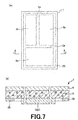
- the sheet material is in a state before being laminated on the electronic substrate, and the average thickness of the first region where the edge of the electronic component is in contact is the first region other than the first region. It is preferable to be configured to be larger than the average thickness of the region 2.
- the plurality of electronic components include two or more electronic components provided side by side,
- the average thickness of the first region that forms a linear shape that continuously contacts the edge of the electronic component provided in parallel is the first region. It is preferable to be configured to be larger than the average thickness of the second region other than.
- the average thickness in the first region of the sheet material is A [ ⁇ m]
- the average thickness in the second region is When the thickness is B [ ⁇ m]
- a / B is preferably 1.05 to 3.
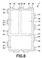
- the sheet material may further include at least one insulating portion provided on the electronic substrate side and at a position corresponding to the edge portion of the base material and separated from the insulating layer. It is preferable to have.
- the at least one insulating portion includes a plurality of the insulating portions provided at intervals from each other along an edge portion of the base material.
- the insulating portion is formed in a frame shape along the edge of the base material.
- the average thickness of the insulating portion is smaller than the average thickness of the insulating layer.
- the portion of the sheet material provided with the insulating portion constitutes a gripping portion that is gripped when the sheet material is separated from the electronic substrate.
- the sheet material of the present invention is laminated on an electronic board including a wiring board having a mounting surface and a plurality of electronic components mounted on the mounting surface of the wiring board, and the electronic board via a ground portion.
- a sheet material used to be fixed to In a state where the sheet material is laminated on the electronic substrate, a sheet-like base material having conductivity in contact with the ground portion, In a state where the sheet material is laminated on the electronic substrate, the sheet material is positioned on the electronic substrate side of the base material and has at least one insulating layer having a size including at least one electronic component. .
- the base material is provided in contact with the insulating layer and has a first part having adhesiveness, and a second part provided on the opposite side of the first part to the insulating layer. It is preferable to have this part.
- the first portion contains a first resin and first conductive particles dispersed in the first resin
- the second portion includes a second resin. It is preferable to contain a resin and second conductive particles dispersed in the second resin in an amount larger than the content of the first conductive particles in the first portion.
- the content of the first conductive particles in the first portion is preferably 1 to 100 parts by weight with respect to 100 parts by weight of the first resin.
- the content of the second conductive particles in the second portion is preferably 100 to 1500 parts by weight with respect to 100 parts by weight of the second resin.
- the shape of the first conductive particles is preferably different from the shape of the second conductive particles.
- the first conductive particles preferably have a dendritic shape or a spherical shape.
- the present invention having the above configuration, by using a sheet material having high flexibility, it is not necessary to consider the damage of the electronic component when the sheet material is laminated on the wiring board. For this reason, it becomes possible to narrow the space
- the present invention it is easy to remove the heat generated from the electronic component, and the thin and highly reliable electronic element can exhibit a sufficient electromagnetic wave shielding effect and the obtained electronic element can be thinned.
- Sheet material can be provided.
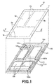
- FIG. 1 is an exploded perspective view showing the configuration of the electronic device of the present invention.
- FIG. 2 is a longitudinal cross-sectional view (a cross-sectional view taken along line AA in FIG. 1) showing the configuration of the sheet material according to the first embodiment (a state bonded to the electronic substrate).
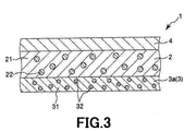
- FIG. 3 is an enlarged cross-sectional view illustrating the configuration of the sheet material according to the second embodiment (a state before being bonded to the electronic substrate).
- FIG. 4 is an enlarged cross-sectional view illustrating a configuration of the sheet material according to the third embodiment (a state before being bonded to the electronic substrate).
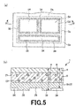
- FIGS. 5A and 5B are diagrams (a) is a plan view showing the vicinity of the insulating layer, and FIG.
- FIG. 5B is a plan view showing the structure of the sheet material according to the fourth embodiment (before being bonded to the electronic substrate).
- FIG. 3 is a diagram showing a central portion in a cross section taken along line BB.
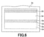
- FIG. 6 is a plan view showing another configuration of the sheet material according to the fourth embodiment (a state before being bonded to the electronic substrate).
- 7A and 7B are diagrams showing the configuration of the sheet material according to the fifth embodiment (the state before being bonded to the electronic substrate), where FIG. 7A is a plan view and FIG. 7B is a cross-sectional view taken along line CC in FIG. The figure which shows the center part and edge part in FIG.
- FIG. 8 is a plan view illustrating another configuration of the sheet material according to the fifth embodiment (a state before bonding to the electronic substrate).
- FIG. 9 is a longitudinal sectional view showing the configuration of the end of the electronic device of the sixth embodiment.
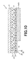
- FIG. 10 is an enlarged cross-sectional view illustrating a configuration of the sheet material according to
- FIG. 1 is an exploded perspective view showing the configuration of the electronic device of the present invention.
- the upper side in FIG. 1 is “upper” and the lower side is “lower”.
- the electronic element 10 of the present invention includes an electronic substrate 100 and a sheet material 1 bonded (laminated) to the electronic substrate 100.
- the electronic substrate 100 First, prior to the description of the sheet material 1, the electronic substrate 100 will be described.
- the electronic board 100 include a flexible printed board, a rigid printed board, and a rigid flexible board.
- the electronic substrate 100 includes a wiring substrate 110 having a mounting surface 101 and a plurality of semiconductor chips (electronic components) 120 mounted on the mounting surface 101 of the wiring substrate 110.
- the semiconductor chip 120 include a CPU chip, a memory chip, a power supply chip, and a sound source chip.
- the wiring substrate 110 includes a substrate 111, a wiring 112 formed on the substrate 111, and a ground wiring (ground portion) 113.
- One end of the wiring 112 is connected to the power supply, and the other end is connected to a terminal of the semiconductor chip 120.
- the ground wiring 113 is formed in a frame shape so as to avoid the wiring 112 and is grounded.
- the mounting surface 101 is partitioned into first to third mounting regions 101a to 101c by the ground wiring 113 as shown in FIG.
- a predetermined semiconductor chip 120 is mounted on each of the mounting regions 101a to 101c.
- the sheet material 1 is bonded to the electronic substrate 100 having such a configuration. Hereinafter, the sheet material 1 will be described.
- FIG. 2 is a longitudinal cross-sectional view (a cross-sectional view taken along line AA in FIG. 1) showing the configuration of the sheet material according to the first embodiment (a state bonded to the electronic substrate).
- the upper side in FIG. 2 is “upper” and the lower side is “lower”.
- the sheet material 1 includes a sheet-like base material 2 having conductivity, an insulating layer 3 provided on the lower surface (one surface) of the base material 2, and the upper surface (the other side) of the base material 2. And a hard coat layer 4 provided on the surface.
- the sheet material 1 is bonded to the electronic substrate 100 with the insulating layer 3 facing the electronic substrate 100.
- the substrate 2 only needs to have conductivity, and may be formed of a metal film.
- the resin film including the solidified or cured product of the resin 21 and the conductive particles 22 is used. It is preferable that it is comprised.
- the substrate 2 may be a combination of these metal films and resin films, or may be a combination of two or more different resin films. The configuration of such a combination will be described in a later embodiment.
- this metal film can be formed using the thing similar to the metal quoted in the electroconductive particle 22.
- the conductivity of the base material 2 can be set to isotropic conductivity or anisotropic conductivity according to the type (purpose) of the wiring board 110.
- the isotropic conductivity means that the base material 2 has conductivity in the thickness direction and the surface direction
- the anisotropic conductivity means that the base material 2 has conductivity only in the thickness direction. Say that.
- Examples of the resin 21 include thermoplastic resins, curable resins, and the like, and one or more of these can be used in combination.
- Examples of the curable resin include a thermosetting resin, a photocurable resin, an anaerobic curable resin, a reaction curable resin, and the like. At least one of the thermosetting resin and the photocurable resin is used. preferable. The effect obtained by using at least one of a curable resin, in particular, a thermosetting resin and a photocurable resin, as the resin 21 will be described later.
- thermoplastic resin examples include polyolefin resins, vinyl resins, styrene / acrylic resins, diene resins, terpene resins, petroleum resins, cellulose resins, polyamide resins, polyurethane resins, polyester resins, Examples thereof include polycarbonate resins and fluorine resins.
- the thermosetting resin may be a resin having at least one functional group in one molecule that can be used for a crosslinking reaction by heating.
- this functional group for example, hydroxyl group, phenolic hydroxyl group, methoxymethyl group, carboxyl group, amino group, epoxy group, oxetanyl group, oxazoline group, oxazine group, aziridine group, thiol group, isocyanate group, blocked isocyanate group, Examples thereof include a blocked carboxyl group and a silanol group.
- thermosetting resins include, for example, acrylic resins, maleic resins, polybutadiene resins, polyester resins, polyurethane resins, urea resins, epoxy resins, oxetane resins, phenoxy resins, Polyimide resin, polyamide resin, polyamideimide resin, phenol resin, cresol resin, melamine resin, alkyd resin, amino resin, polylactic acid resin, oxazoline resin, benzoxazine resin, silicone resin And fluorine-based resins.
- acrylic resins acrylic resins, maleic resins, polybutadiene resins, polyester resins, polyurethane resins, urea resins, epoxy resins, oxetane resins, phenoxy resins, Polyimide resin, polyamide resin, polyamideimide resin, phenol resin, cresol resin, melamine resin, alkyd resin, amino resin, polylactic acid resin, oxazoline resin, benzoxazine resin, silicone resin And fluorine-based resin
- the base material 2 is made of a curing agent such as a resin or a low-molecular compound that reacts with the functional group to form a chemical crosslink in addition to the thermosetting resin. It is preferable to include.
- a curing agent is not particularly limited.
- a curing agent capable of causing a curing reaction to proceed at a relatively high temperature such as a phenolic curing agent such as a phenol novolac resin, or an amine curing agent such as dicyandiamide or aromatic diamine.
- the curing agent examples include an curing agent, an isocyanate curing agent, an epoxy curing agent, an aziridine curing agent, and a metal chelate curing agent that can cause the curing reaction to proceed at a relatively low temperature (for example, 120 ° C. or less).
- the photocurable resin may be a resin having one or more unsaturated bonds in one molecule that cause a crosslinking reaction by light.
- the photocurable resin include, for example, acrylic resins, maleic resins, polybutadiene resins, polyester resins, polyurethane resins, epoxy resins, oxetane resins, phenoxy resins, polyimide resins, polyamides. Resin, phenol resin, alkyd resin, amino resin, polylactic acid resin, oxazoline resin, benzoxazine resin, silicone resin, fluorine resin and the like.
- the conductive particles 22 are dispersed in such a solidified or cured product of the resin 21.
- the base material 2 sheet material 1
- the conductive particles 22 include metal particles, carbon particles, conductive resin particles, and the like, and one or more of these can be used in combination.
- the metal constituting the metal particles examples include gold, platinum, silver, copper, nickel, aluminum, iron or alloys thereof, ITO, ATO, etc., but copper is preferable from the viewpoint of price and conductivity.
- the metal particle may be a particle including a core made of metal and a coating layer that covers the core and is made of metal. Examples of such metal particles include silver-coated copper particles obtained by coating a nucleus composed of copper with a coating layer composed of silver.
- examples of carbon constituting the carbon particles include acetylene black, ketjen black, furnace black, carbon nanotube, carbon nanofiber, graphite, fullerene, graphene and the like.
- examples of the conductive resin constituting the conductive resin particles include poly (3,4-ethylenedioxythiophene), polyacetylene, polythiophene, and the like.
- the average particle diameter of the conductive particles 22 is preferably about 1 to 100 ⁇ m, more preferably about 3 to 75 ⁇ m, and further preferably about 5 to 50 ⁇ m.
- the filling rate of the conductive particles 22 in the substrate 2 can be improved. For this reason, the electromagnetic wave shielding effect of the base material 2 (sheet material 1) can be improved more.
- the resin composition is prepared by mixing with the resin 21, the fluidity is improved, so that the moldability to the substrate 2 is improved.
- the shape of the conductive particles 22 may be any shape such as a spherical shape, a needle shape, a flake shape, or a dendritic shape.
- the average particle diameter of the conductive particles 22 can be obtained by measurement using a general laser diffraction method, scattering method, or the like, and the average value of diameters assuming a circle equal to the projected area of the fine particle aggregate. Can be the average particle size.
- the content of the conductive particles 22 in the substrate 2 is not particularly limited, but is preferably 100 to 1500 parts by weight, more preferably 100 to 1000 parts by weight with respect to 100 parts by weight of the resin 21. .
- the base material 2 can be provided with necessary and sufficient conductivity regardless of the type of the conductive particles 22.
- the electromagnetic wave shielding effect can be sufficiently enhanced.
- liquidity of the resin composition containing the resin 21 and the electroconductive particle 22 increases, and it is preferable also from becoming easy to form the base material 2.
- the average thickness of the substrate 2 is not particularly limited, but is preferably about 2 to 500 ⁇ m, and more preferably about 5 to 100 ⁇ m. By making the average thickness of the base material 2 within the above range, it is possible to reduce the thickness of the base material 2 while preventing the mechanical strength of the base material 2 from being lowered.
- the base material 2 is, for example, a colorant (pigment, dye), a flame retardant, a filler (inorganic additive), a lubricant, an antiblocking agent, a metal deactivator, a thickener, a dispersant, a silane coupling.
- a colorant pigment, dye
- a filler inorganic additive
- a lubricant for example, a lubricant
- an antiblocking agent e.g., stannous, sodium sulfate
- a metal deactivator e.g., sodium bicarbonate
- a thickener e.g., sodium bicarbonate
- dispersant e.g., sodium silane coupling
- silane coupling e.g., sodium silane coupling
- Agents rust inhibitors, copper damage inhibitors, reducing agents, antioxidants, tackifier resins, plasticizers, ultraviolet absorbers, antifoaming agents, leveling regulators, and the like.
- Examples of the colorant include organic pigments, carbon black, ultramarine blue, petals, zinc white, titanium oxide, graphite and the like.
- Examples of the flame retardant include a halogen-containing flame retardant, a phosphorus-containing flame retardant, a nitrogen-containing flame retardant, and an inorganic flame retardant.
- Examples of the filler include glass fiber, silica, talc, and ceramic.
- examples of the lubricant include fatty acid esters, hydrocarbon resins, paraffin, higher fatty acids, fatty acid amides, aliphatic alcohols, metal soaps, modified silicones, and the like.
- examples of the anti-blocking agent include calcium carbonate, silica, polymethylsilsesquiosan, aluminum silicate salt and the like.
- the insulating layer 3 is provided on the lower surface (surface on the electronic substrate 100 side) of the base material 2.
- the first insulating layer 3 a corresponding to the first mounting region 100 a of the mounting surface 101 (wiring substrate 110) and the second mounting are formed on the lower surface of the base material 2.
- a second insulating layer 3b corresponding to the region 100b and a third insulating layer 3c corresponding to the third mounting region 100c are provided.
- Each of the first to third insulating layers 3a to 3c (hereinafter collectively referred to simply as “insulating layer 3”) is smaller than the substrate 2 in plan view, and is a sheet.
- the size includes one or more semiconductor chips 120.
- a strip-shaped exposed region 2a exposed from the first to third insulating layers 3a to 3c is formed on the lower surface of the substrate 2. Therefore, the exposed region 2 a has a shape corresponding to the shape of the ground wiring 113 of the wiring board 110.
- the exposed region 2a of the base material 2 constitutes a connecting portion (joining portion) that connects (joins) the sheet material 1 to the wiring board 110.
- the cured product is obtained by curing the curable resin after bringing the exposed region 2 a of the base material 2 into contact with the ground wiring 113 of the wiring substrate 110.
- the sheet material 1 and the electronic substrate 100 can be joined (fixed) at the contact portion.
- the insulating layer 3 only needs to have sufficient insulating properties, and can be formed using a hard resin or a curable resin (particularly a thermosetting resin).
- a hard resin include acrylic, polyurethane, polyurethane urea, epoxy, epoxy ester, polyester, polycarbonate, polyphenylene sulfide, and the like, and one or more of these can be used in combination.
- the curable resin the same curable resin as mentioned in the resin 21 can be used.
- the insulating layer 3 may contain the same curing agent as described in the base material 2.
- the degree of curing (fully cured or semi-cured state) of the insulating layer 3 in the sheet material 1 before lamination (before use) on the electronic substrate 100 the degree of fluidity (solid state or gel state), and adhesiveness.
- the degree of curing can be controlled.
- the insulating layer 3 includes, for example, a colorant (pigment, dye), a flame retardant, a filler (inorganic additive), a lubricant, an antiblocking agent, a metal deactivator, a thickener, a dispersant, a silane coupling.
- a colorant pigment, dye
- a flame retardant for example, a flame retardant, a filler (inorganic additive), a lubricant, an antiblocking agent, a metal deactivator, a thickener, a dispersant, a silane coupling.
- a colorant pigment, dye
- a filler inorganic additive
- the average thickness of the insulating layer 3 is not particularly limited, but is preferably about 50 to 200 when the average thickness of the substrate 2 is 100, more preferably about 75 to 150. preferable. Specifically, the average thickness of the insulating layer 3 is preferably about 1 to 1000 ⁇ m, and more preferably about 3 to 200 ⁇ m. Thereby, the insulating layer 3 can impart excellent followability to the surface of the electronic substrate 100 to the insulating layer 3 (sheet material 1) while maintaining sufficient insulation.
- the insulating layer 3 and the surface of the semiconductor chip 120 are in close contact with each other.
- the adhesion of the insulating layer 3 to the surface of the semiconductor chip 120 can be further improved.
- this operation may be performed under reduced pressure or vacuum when the sheet material 1 is bonded to the electronic substrate 100.
- the lower surface of the insulating layer 3 may be a smooth surface or a rough surface. If the lower surface of the insulating layer 3 (surface on the electronic substrate 100 side) is a smooth surface, the contact area between the insulating layer 3 and the surface of the semiconductor chip 120 can be increased, and the heat dissipation effect of the sheet material 1 can be improved. Can do. On the other hand, when the lower surface of the insulating layer 3 is formed of a rough surface, the contact area between the insulating layer 3 and the surface of the semiconductor chip 120 can be slightly reduced, and when the electronic substrate 100 is recycled, the insulating layer 3 ( The sheet material 1) can be removed more easily.
- a hard coat layer (protective layer) 4 having a function of protecting the base material 2 is provided on the upper surface of the base material 2 (the surface opposite to the electronic substrate 100). Thereby, damage to substrate 2 can be prevented suitably.
- Such a hard coat layer 4 includes, for example, a bifunctional or monofunctional or monofunctional monomer having an ⁇ , ⁇ -unsaturated double bond, a vinyl monomer, an allyl monomer, a monofunctional (meth) acrylate monomer, a polyfunctional monomer, It is preferably composed of a polymer (cured product) of a radical polymerization monomer such as a functional (meth) acrylate monomer.
- a radical polymerization monomer such as a functional (meth) acrylate monomer.
- the bifunctional or higher monomer having an ⁇ , ⁇ -unsaturated double bond is, for example, a relatively low molecular weight monomer having a molecular weight of less than 1000 (so-called narrowly-defined monomer), for example, having a weight average molecular weight of 1000 or more. It may be a relatively high molecular weight oligomer or prepolymer of less than 10,000.
- examples of the oligomer having an ⁇ , ⁇ -unsaturated double bond include polyester (meth) acrylate, polyurethane (meth) acrylate, epoxy (meth) acrylate, (meth) acrylated maleic acid-modified polybutadiene, and the like. It is done.
- vinyl monomer examples include styrene, ⁇ -methylstyrene, divinylbenzene, N-vinylpyrrolidone, vinyl acetate, N-vinylformaldehyde, N-vinylcaprolactam, alkyl vinyl ether and the like.
- allyl monomers include trimethacryl isocyanurate and triallyl cyanurate.
- Examples of monofunctional (meth) acrylate monomers include 2- (meth) acryloyloxyethyl phthalate, 2- (meth) acryloyloxyethyl-2-hydroxyethyl phthalate, and 2- (meth) acryloyloxyethyl hexahydro.
- polyfunctional (meth) acrylate monomer examples include 1,3-butylene glycol di (meth) acrylate, 1,4-butanediol di (meth) acrylate, 1,6-hexanediol di (meth) acrylate, 1, 9-nonanediol di (meth) acrylate, bisphenol A di (meth) acrylate, bisphenol F di (meth) acrylate, diethylene glycol di (meth) acrylate, hexahydrophthalic acid di (meth) acrylate, hydroxypivalate neopentyl glycol di (Meth) acrylate, neopentyl glycol di (meth) acrylate, hydroxypivalate ester neopentyl glycol di (meth) acrylate, pentaerythritol di (meth) acrylate, di (meth) acrylate phthalate Polyethylene glycol di (meth) acrylate, poly(
- the hard coat layer 4 is made of, for example, a polyester resin such as polyethylene terephthalate (PET) or polybutylene terephthalate (PBT), an acrylic resin such as polymethyl methacrylate, polyethylene, polypropylene, ethylene-vinyl acetate copolymer. It can also be composed of a thermoplastic resin such as a polyolefin-based resin such as a coalescence.
- a polyester resin such as polyethylene terephthalate (PET) or polybutylene terephthalate (PBT)
- an acrylic resin such as polymethyl methacrylate
- polyethylene polypropylene
- ethylene-vinyl acetate copolymer ethylene-vinyl acetate copolymer
- thermoplastic resin such as a polyolefin-based resin such as a coalescence.
- the hard coat layer 4 is, for example, a colorant (pigment, dye), a flame retardant, a filler (inorganic additive), a lubricant, an antiblocking agent, a metal deactivator, a thickener, a dispersant, a silane cup.
- a ring agent, a rust preventive agent, a copper damage inhibitor, a reducing agent, an antioxidant, a tackifier resin, a plasticizer, an ultraviolet absorber, an antifoaming agent, a leveling regulator, and the like may be contained.
- the average thickness of the hard coat layer 4 is not particularly limited, but is preferably about 0.1 to 10 ⁇ m, preferably 0.5 to 5 ⁇ m. More preferred is the degree.
- the average thickness of the hard coat layer 4 is preferably about 1 to 50 ⁇ m, and more preferably about 5 to 30 ⁇ m.
- the protective layer is not limited to the hard coat layer 4 and may be a cushion layer, a print layer, or the like that absorbs external stress or impact, and is a laminate in which these layers are combined. Also good.
- the sheet material 1 as described above can be manufactured, for example, as follows.
- the resin composition for a hard coat layer on a release sheet After applying the resin composition for a hard coat layer on a release sheet, it is cured or solidified. Thereby, the hard coat layer 4 is obtained.
- the base material resin composition is applied onto the hard coat layer 4, it is semi-cured, cured or solidified. Thereby, the base material 2 is obtained. In this state, the base material 2 may or may not have adhesiveness.
- the insulating layer resin composition is coated on the substrate 2, it is semi-cured, cured or solidified. Thereby, the insulating layer 3 is obtained. In this state, the insulating layer 3 may or may not have adhesiveness.
- Examples of methods for applying each resin composition include gravure coating, kiss coating, die coating, lip coating, comma coating, blade coating, roll coating, knife coating, spray coating, and bar coating.
- a spout coat method, a dip coat method, or the like can be used.
- seat material 1 may be made to join these layers mutually.
- a heat conduction layer for example, a water vapor barrier layer, an oxygen barrier layer, a low dielectric constant layer, a high dielectric constant layer,
- a heat conduction layer for example, a heat conduction layer, a water vapor barrier layer, an oxygen barrier layer, a low dielectric constant layer, a high dielectric constant layer,
- a heat conduction layer for example, a heat conduction layer, a water vapor barrier layer, an oxygen barrier layer, a low dielectric constant layer, a high dielectric constant layer,
- a low dielectric loss tangent layer for example, a heat conduction layer, a water vapor barrier layer, an oxygen barrier layer, a low dielectric constant layer, a high dielectric constant layer,
- a heat resistant layer for example, a heat conduction layer, a water vapor barrier layer, an oxygen barrier layer, a low dielectric constant layer, a high dielectric constant layer,
- a heat conduction layer for example, a water vapor barrier layer, an oxygen barrier layer,
- Such a sheet material 1 is bonded to the electronic substrate 100 as follows.
- the sheet material 1 is laminated on the electronic substrate 100 with the insulating layer 3 facing the electronic substrate 100 side.
- the insulating layer 3 is in close contact with the surface of the semiconductor chip 120, and the exposed region 2a of the base material 2 is in contact with the ground wiring 113.
- the sheet material 1 is fixed (bonded) to the electronic substrate 100.
- the electronic element 10 is obtained.
- the degree of adhesion of the insulating layer 3 to the surface of the semiconductor chip 120 is increased by performing thermocompression bonding under reduced pressure or vacuum. As a result, not only the electromagnetic wave shielding effect by the sheet material 1 but also a good heat dissipation effect is exhibited.
- the thermosetting resin is cured by the heating and pressing, and the exposed region 2a of the substrate 2 is grounded by the cured product.
- the wiring 113 is firmly joined.
- the mechanical strength of the base material 2 (sheet material 1) itself is also improved by the curing of the thermosetting resin.
- the base material 2 contains a photocurable resin, light (active radiation) is irradiated to the exposed area
- a brazing material (solder) is provided on the ground wiring 113 prior to the thermocompression bonding, so that the exposed region 2a of the base material 2 becomes the ground wiring 113. It is firmly joined through the brazing material.
- Such an electronic element 10 is easy to remove heat from the semiconductor chip 120, is thin, and has high reliability.
- a mobile phone such as a smartphone, a personal computer, a tablet terminal, LED lighting, It can be used for in-vehicle parts such as organic EL lighting, liquid crystal television, organic EL television, digital camera, digital video camera and automobile.
- FIG. 3 is an enlarged cross-sectional view showing the configuration of the sheet material according to the second embodiment (a state before being bonded to the electronic substrate).
- the second embodiment will be described, the description will focus on the differences from the first embodiment, and the description of the same matters will be omitted.
- the upper side in FIG. 3 is “upper” and the lower side is “lower”.
- the sheet material 1 of the second embodiment is the same as the first embodiment except for the configuration of the insulating layer 3 (first to third insulating layers 3a to 3c). That is, as shown in FIG. 3, the insulating layer 3 of the second embodiment includes a resin 31 and thermally conductive particles 32 dispersed in the resin 31 and having a thermal conductivity higher than that of the resin 31. Including. By including the heat conductive particles 32 in the insulating layer 3, the heat conductivity of the sheet material 1 is improved, and the heat dissipation effect by the sheet material 1 is further increased.
- Examples of the constituent material of the heat conductive particles 32 include metal oxides such as calcium oxide, magnesium oxide, and aluminum oxide, metal hydroxides such as aluminum hydroxide and magnesium hydroxide, aluminum nitride, and boron nitride.
- Metal carbonates such as calcium carbonate, magnesium carbonate, metal silicates such as calcium silicate, crystalline silica, amorphous silica, silicon compounds such as silicon carbide, etc. 1 type or 2 types or more can be used in combination.
- the constituent material of the thermally conductive particles 32 is preferably at least one of aluminum oxide, aluminum nitride, and boron nitride, and aluminum oxide is more preferable because of high heat resistance and insulation reliability. Further, spherical aluminum oxide is excellent in that it can be closely packed in the insulating layer 3, and is particularly preferable in that it can prevent the elastic modulus of the insulating layer 3 from being unnecessarily increased even when the filling amount is increased.
- the heat conductive particles 32 may include a plurality of types of particles.
- the average particle diameter of the heat conductive particles 32 is not particularly limited, but is preferably about 0.1 to 250 ⁇ m, and more preferably about 0.5 to 100 ⁇ m. Since the heat conductive particles 32 having such an average particle diameter are easily dispersed uniformly in the insulating layer 3, the heat conductivity of the insulating layer 3 can be further increased.
- the shape of the heat conductive particles 32 may be any shape such as a spherical shape, a needle shape, a flake shape, or a dendritic shape.
- the average particle diameter of the heat conductive particles 32 can be obtained by measurement using a general laser diffraction method, scattering method, or the like, and the average diameter when a circle equal to the projected area of the fine particle aggregate is assumed. The value can be the average particle size.
- the content of the heat conductive particles 32 in the insulating layer 3 is not particularly limited, but is preferably about 25 to 95% by weight, and more preferably about 35 to 85% by weight. By making the content of the heat conductive particles 32 in the insulating layer 3 within the above range, the thermal conductivity of the insulating layer 3 is sufficiently improved while preventing the mechanical strength of the insulating layer 3 from being lowered. Can do.
- the same resin that can be used for the insulating layer 3 in the first embodiment can be used.
- the insulating layer 3 may contain the same curing agent as described in the first embodiment.
- FIG. 4 is an enlarged cross-sectional view showing a configuration of the sheet material according to the third embodiment (a state before being bonded to the electronic substrate).
- the third embodiment will be described. The description will focus on the differences from the first embodiment, and the description of the same matters will be omitted. In the following, for convenience of explanation, the upper side in FIG. 4 is “upper” and the lower side is “lower”.
- the sheet material 1 of the third embodiment is the same as the first embodiment except that the configuration of the base material 2 is different. That is, as shown in FIGS. 4A and 4B, the base material 2 of the third embodiment includes a main body portion 20 including a resin 21 and conductive particles 22, and the insulating layer 3 side of the main body portion 20. And a metal film 23 provided in contact with the main body 20. When the base material 2 includes the metal film 23, the electromagnetic wave shielding effect and the heat dissipation effect of the base material 2 (sheet material 1) are more suitably exhibited.
- the metal film 23 is formed by attaching (joining) a metal foil formed of the metal mentioned in the conductive particle 22 to the main body 20, or the metal oxide (eg, ITO, ATO) mentioned in the conductive particle 22.
- a method of forming a deposited film or a sputtering film on the main body 20 by vapor deposition or sputtering, a method of forming a printed film on the main body 20 by printing a conductive paste (for example, silver paste), etc. Can be obtained.
- various copper foil is preferable from the surface of electroconductivity and cost, and rolled copper foil or electrolytic copper foil is more preferable.
- the average thickness of the metal film 23 is not particularly limited, but is preferably about 0.004 to 2500% of the average thickness of the base material 2, and preferably about 0.025 to 75%. By making the average thickness of the metal film 23 within the above range, the electromagnetic wave shielding effect and the heat radiation effect of the base material 2 are sufficiently exhibited while preventing the flexibility of the base material 2 (sheet material 1) from being lowered. Is done.
- the specific average thickness of the metal film 23 is preferably as follows.
- the average thickness is preferably about 50 to 300 nm, and more preferably about 75 to 200 nm.
- the average thickness is preferably about 20 to 80 nm, and more preferably about 25 to 70 nm.
- the average thickness is preferably about 0.01 to 20 ⁇ m, and more preferably about 0.1 to 15 ⁇ m.
- the metal film 23 may be substantially the same size as the insulating layer 3 in a plan view, and as shown in FIG. The sizes may be approximately equal.
- the sheet material 1 can be firmly bonded to the electronic substrate 100 using the main body portion 20 of the exposed region 2 a.
- the metal film 23 in the exposed region 2a can be metal-bonded to the ground wiring 113 of the wiring board 110 by, for example, laser irradiation. For this reason, extremely high joining between the sheet material 1 and the electronic substrate 100 is possible.
- such a metal film 23 may have a mesh shape or a shape having a plurality of through holes formed by punching. By making such a shape, water vapor permeability can be imparted to the metal film 23.
- the metal film 23 may be provided so as to be in contact with the main body 20, and may be provided on the hard coat layer 4 side instead of the insulating layer 3 side. These may be provided at any arbitrary position, or a combination thereof.
- FIGS. 5A and 5B are diagrams showing the configuration of the sheet material according to the fourth embodiment (the state before being bonded to the electronic substrate), where FIG. 5A is a plan view showing the vicinity of the insulating layer 3a, and FIG. FIG. 6 is a plan view showing another configuration of the sheet material of the fourth embodiment (a state before being bonded to the electronic substrate).
- the fourth embodiment will be described. The description will focus on the differences from the first embodiment, and the description of the same matters will be omitted. In the following, for convenience of explanation, the upper side in FIG. 5B and FIG. 6 is “upper” and the lower side is “lower”.
- the thickness of the insulating layer 3 is non-uniform in a state before the sheet material 1 is bonded to the electronic substrate 100 (a state before use of the sheet material 1).
- the average thickness of the region 33 is larger than the average thickness of the second region 34 other than the first region 33.
- the first region 33 has a rectangular frame shape in plan view corresponding to the outer peripheral shape of the semiconductor chip 120.
- the average thickness of the first region 33 of the sheet material 1 is A [ ⁇ m]
- the average thickness of the second region 34 is B [ ⁇ m].
- a / B is preferably about 1.05 to 3, more preferably about 1.05 to 1.4, and still more preferably about 1.1 to 1.25.
- Such an insulating layer 3 is formed on the first region 33 of the insulating layer 3 after forming a portion having a uniform thickness on the substrate 2 side of the insulating layer 3 by the method described in the first embodiment. It can be obtained by stacking and forming quadrangular frame shapes.
- the first region 33 is not limited to the region shown in FIG. 5A, and may be a region where the sheet material 1 is particularly easily broken.
- the first region 33 is provided as shown in FIG. 6. Further, it can be a linear region continuously contacting along the edge of the two semiconductor chips 120.
- the extent to which the sheet material 1 is stretched is increased at the locations where the semiconductor chips 120 are densely arranged. For this reason, a linear region straddling the two semiconductor chips 120 as shown in FIG. 6 is defined as the first region 33, and the thickness of the insulating layer 3 (sheet material 1) in the first region 33 is increased. Thus, breakage of the sheet material 1 can be sufficiently prevented.
- the sheet material 1 in the state before the sheet material 1 is bonded to the electronic substrate 100, the sheet material 1 only needs to have an average thickness of the first region 33 larger than an average thickness of the second region 34.
- the base material 2 instead of forming the insulating layer 3 to be partially thick, the base material 2 is partially thick, and the hard coat layer 4 is partially thick. Or a combination thereof.
- FIG. 7A and 7B are diagrams showing the configuration of the sheet material according to the fifth embodiment (the state before being bonded to the electronic substrate), where FIG. 7A is a plan view, and FIG. FIG. 8 is a plan view showing another configuration of the sheet material of the fifth embodiment (a state before being joined to the electronic substrate).
- FIG. 7B the upper side in FIG. 7B is referred to as “upper” and the lower side is referred to as “lower”.
- the sheet material 1 of the fifth embodiment has an insulating portion 35 provided separately from the insulating layer 3 along the edge portion of the lower surface of the base material 2, and otherwise the same as in the first embodiment. It is. That is, as shown in FIGS. 7A and 7B, the insulating portion 35 is formed along the edge of the lower surface of the substrate 2 so as to surround the first to third insulating layers (3a to 3c). It is formed in a rectangular frame shape. With this configuration, it is possible to prevent the base material 2 and the mounting surface 101 of the wiring board 110 from directly contacting each other at the edge of the sheet material 1 in a state where the sheet material 1 is bonded (laminated) to the electronic substrate 100. it can. For this reason, the unintentional short circuit between the base material 2 and the wiring board 110 can be prevented, and the highly reliable electronic device 10 can be obtained.
- the portion of the sheet material 1 on which the insulating portion 35 is formed is gripped, which becomes a trigger for the peeling operation.
- the peeling operation can be easily performed. That is, the portion of the sheet material 1 where the insulating portion 35 is provided constitutes a grip portion that is gripped when the sheet material 1 is separated from the electronic substrate 100 on which the sheet material 1 is laminated.
- the insulating portion 35 is formed in a frame shape along the edge portion of the base material 2, so that the peeling operation is performed from any part of the entire circumference of the sheet material 1. Can start.
- the constituent material of the insulating part 35 is preferably the same as the hard resin mentioned in the insulating layer 3 of the first embodiment.
- the insulating portion 35 By configuring the insulating portion 35 with a hard resin, it is possible to prevent the insulating portion 35 from being bonded to the mounting surface 101 of the wiring substrate 110. For this reason, when the sheet material 1 is peeled from the electronic substrate 100, the portion of the sheet material 1 where the insulating portion 35 is formed can be gripped more easily and reliably.
- the average thickness of the insulating portion 35 is preferably set smaller than the average thickness of the insulating layer 3. Thereby, the insulating part 35 can be made into the state which contacted the mounting surface 101 of the wiring board 110 lightly. For this reason, when the sheet material 1 is peeled off from the electronic substrate 100, the portion of the sheet material 1 on which the insulating portion 35 is formed becomes easier to grip.
- the insulating portion 35 can be formed by, for example, the same method as the insulating layer 3, and may be formed in the same process as the insulating layer 3, or may be formed in a process different from the insulating layer 3. It may be.
- the base member 2 is provided with a plurality of ear portions 24 formed at intervals along the edge portion, and an insulating portion 35 is provided on the lower surface of each ear portion 24. May be. That is, a plurality of insulating portions 35 may be provided along the edge portion of the base material 2 at intervals.
- the electronic substrate 100 can be accommodated in the casing of the electronic device with the ear portion 24 folded. For this reason, it can prevent that the ear
- ear 24 (insulating part 35) may be provided from the viewpoint of starting the peeling operation when the electronic substrate 100 is recycled.
- FIG. 9 is a longitudinal sectional view showing the configuration of the end of the electronic device of the sixth embodiment.
- the sixth embodiment will be described, the description will focus on differences from the first embodiment, and the description of the same matters will be omitted.
- the upper side in FIG. 9 is “upper” and the lower side is “lower”.
- the sheet material 1 of the sixth embodiment includes a base material 2 made of a metal film and an insulating layer 3 provided on the lower surface (one surface) of the base material 2. It has a two-layer structure.
- a plurality of conductive pins 114 are provided on the upper surface of the ground wiring 113 at predetermined intervals along the longitudinal direction of the ground wiring 113. Each conductive pin 114 is arranged with the needle tip (top) facing upward.
- the ground portion is configured by the ground wiring 113 and the conductive pin 114.
- the conductive pin 114 may be formed integrally with the ground wiring 113.
- the ground wiring 113 may be omitted and the conductive pin 114 may be directly grounded.
- Such conductive pins 114 can be formed using the same metals as those mentioned in the conductive particles 22 of the first embodiment.
- the sheet material 1 may have the same configuration as the sheet material 1 of the first to fifth embodiments.
- FIG. 10 is an enlarged cross-sectional view illustrating the configuration of the sheet material according to the seventh embodiment (a state before being bonded to the electronic substrate).
- the seventh embodiment will be described, the description will focus on the differences from the first embodiment, and description of similar matters will be omitted.
- the upper side in FIG. 10 is “upper” and the lower side is “lower”.
- the sheet material 1 of the seventh embodiment is the same as the first embodiment except that the configuration of the base material 2 is different. That is, as shown in FIG. 10, the base material 2 of the seventh embodiment includes a lower layer (first portion) 2 ⁇ / b> X provided in contact with the insulating layer 3, and the lower layer 2 ⁇ / b> X (on the opposite side to the insulating layer 3). ) Provided on the upper layer (second portion) 2Y.
- the lower layer 2X includes a resin (first resin) 25 and conductive particles (first conductive particles) 26 dispersed in the resin 25, and the upper layer 2Y includes a resin (second resin) 21. And conductive particles (second conductive particles) 22 dispersed in the resin 21. Further, the content in the upper layer 2Y of the conductive particles 22 is set to be larger than the content in the lower layer 2X of the conductive particles 25.
- the upper layer 2Y can exhibit high electromagnetic shielding properties, and the lower layer 2X can be provided with adhesiveness depending on the type of the resin 25 and the like. Therefore, when the sheet material 1 of this embodiment is laminated on the electronic substrate 100, the exposed region 2a of the sheet material 1 (base material 2) is attached to the ground wiring 113 by using the adhesiveness of the lower layer 2X. And can be fixed.
- thermocompression bonding the sheet material 1 to the electronic substrate 100 is omitted, that is, the sheet material 1 is attached to the electronic substrate 100 manually by the operator. Can do. Therefore, the production efficiency of the electronic substrate 100 can be improved. Moreover, since the operation of thermocompression bonding can be omitted, the semiconductor chip 120 can be prevented from being deteriorated by heating at this time, and the electronic element 10 with higher reliability can be obtained.
- the resin 25 is preferably a resin (including rubber) having a glass transition temperature of 0 ° C. or lower, and a resin (including rubber) having a glass transition temperature of ⁇ 10 ° C. or lower from the viewpoint of imparting higher adhesion to the lower layer 2X. More preferably, a resin (including rubber) having a glass transition temperature of ⁇ 20 ° C. or lower is more preferable. Specific examples of such resins (including rubber) include various resins such as acrylic resins and urethane resins, various rubbers such as natural rubber and synthetic rubber, and various thermoplastics such as styrene block copolymers. An elastomer etc. are mentioned. Further, the lower layer 2X may contain the same curing agent as described in the first embodiment.
- the lower layer 2X may have either isotropic conductivity or anisotropic conductivity, but preferably has anisotropic conductivity. Thereby, the electric current which flows into upper layer 2Y can be smoothly transmitted by ground wiring 113 via lower layer 2X, and the electromagnetic wave shielding effect of substrate 2 (sheet material 1) is more suitably exhibited.
- the conductive particles 26 dispersed in the resin 25 particles having the same kind and average particle diameter as the conductive particles 22 described in the first embodiment can be used.
- the shape of the conductive particles 26 can also be the same shape as the conductive particles 22 described in the first embodiment, but is preferably dendritic or spherical.
- the dendritic or spherical conductive particles 26 can impart necessary and sufficient conductivity to the lower layer 2X even if the content in the lower layer 2X is relatively small.
- the adhesiveness of lower layer 2X can be improved more by making content in the lower layer 2X of the electroconductive particle 26 into a small quantity.
- the content of the conductive particles 26 in the lower layer 2X is preferably 1 to 100 parts by weight and more preferably 10 to 50 parts by weight with respect to 100 parts by weight of the resin 25.
- the resin 21 and the conductive particles 22 contained in the upper layer 2Y provided on the lower layer 2X can have the same configuration as described in the first embodiment.
- the upper layer 2Y may contain the same curing agent as described in the first embodiment.
- the upper layer 2Y may have either isotropic conductivity or anisotropic conductivity, but preferably has isotropic conductivity. Thereby, electromagnetic waves can be reliably captured by the upper layer 2Y, and the converted current can be quickly transmitted to the lower layer 2X.
- the lower layer 2X an anisotropic conductivity that is different from the isotropic conductivity of the upper layer 2Y
- the lower layer 2X and the upper layer 2Y can share different roles, and the base material 2 (sheet material 1 The electromagnetic wave shielding effect of) is more suitably exhibited.
- the shape of the conductive particles 22 is preferably different from the conductive particles 26 (particularly flakes).
- the upper layer 2 ⁇ / b> Y can contain a large amount of the conductive particles 22 and can have sufficient isotropic conductivity.
- the content in the upper layer 2Y of the conductive particles 22 is preferably 100 to 1500 parts by weight, more preferably 100 to 1000 parts by weight with respect to 100 parts by weight of the resin 21.
- the content in the upper layer 2Y of the conductive particles 22 is preferably 100 to 1500 parts by weight, more preferably 100 to 1000 parts by weight with respect to 100 parts by weight of the resin 21.
- the average thickness of the lower layer 2X is Tx [ ⁇ m] and the average thickness Ty [ ⁇ m] of the upper layer 2Y
- these ratios Ty / Tx are not particularly limited. It is preferably about 1 to 7.5, and more preferably about 2 to 5.
- the base material 2 that exhibits a higher electromagnetic shielding effect is obtained.
- the average thickness of the lower layer 2X is preferably about 0.5 to 150 ⁇ m, more preferably about 1.5 to 25 ⁇ m, and the average thickness of the upper layer 2Y is 1.5 to The thickness is preferably about 350 ⁇ m, more preferably about 3.5 to 75 ⁇ m.
- the upper layer 2Y may be composed of the same metal film as described in the third and sixth embodiments.
- the insulating layer 3 is provided on the lower surface (surface on the electronic substrate 100 side) of the base material 2.
- the insulating layer 3 can have the same configuration as described in the first or second embodiment, and also uses a resin composition containing the same resin 21 and curing agent as the upper layer 2Y. Can be formed.
- the insulating layer 3 may or may not have adhesiveness.
- the sheet material 1 of the present embodiment is preferably attached to the electronic substrate 100 manually by the operator.
- the insulating layer 3 has adhesiveness, the sheet material 1 can be easily positioned with respect to the electronic substrate 100 and the production efficiency of the electronic element 10 can be further improved. If the sheet material 1 is not sticky, the sheet material 1 is easily peeled off from the electronic substrate 100 even if it is once attached to the electronic substrate 100, and the position of the sheet material 1 relative to the electronic substrate 100 can be easily corrected.
- the sheet material 1 is fixed (laminated) to the electronic substrate 100 and then the layer is in this state. May be post-cured. Thereby, while being able to join the sheet material 1 to the electronic substrate 100, the mechanical strength of the sheet material 1 can also be improved.
- the lower layer 2X is made of a resin (including rubber) having a glass transition temperature of 0 ° C. or lower, a first curing agent capable of causing a curing reaction to proceed at a relatively low temperature as described in the first embodiment, If formed using a resin composition containing a second curing agent capable of causing a curing reaction to proceed at a higher temperature than the first curing agent and the conductive particles 26, the first material is used before the sheet material 1 is used.
- the lower layer 2X is made into a gel state (semi-solid state) by the action of the curing agent, and the lower layer 2X is made into a solid state by the action of the second curing agent by post-curing after the sheet material 1 is fixed (laminated) to the electronic substrate 100. It can be.
- the sheet material 1 is manufactured by forming the hard coat layer 4, the upper layer 2Y, the lower layer 2X, and the insulating layer 3 by coating the resin composition constituting each layer in the same manner as in the first embodiment. can do.
- the sheet material 1 since the lower layer 2X has adhesiveness, the sheet material 1 is prepared by previously preparing a laminated body in which the hard coat layer 4, the upper layer 2Y, and the lower layer 2X are laminated, and the insulating layer 3 created separately. You may manufacture by sticking to the lower layer 2X of a laminated body.
- one or more intermediate layers for any purpose may be provided between the lower layer 2X and the upper layer 2Y.
- an intermediate layer include an adhesion layer for improving adhesion between the lower layer 2X and the upper layer 2Y, the metal film 23 of the third embodiment, and the like.
- the adhesion layer is preferably composed of, for example, a mixture of a resin composition constituting the lower layer 2X and a resin composition constituting the upper layer 2Y.
- seat material can be substituted with the thing of the arbitrary structures which can exhibit the same function.
- arbitrary components may be added.
- the electronic element and the sheet material may be combined with any one of the first to seventh embodiments.
- the sheet material of each said embodiment has a hard-coat layer (protective layer), what is necessary is just to provide a hard-coat layer (protective layer) as needed, and can also be abbreviate
- the ground portion is not particularly limited as long as it can ground the base material of the sheet material (connected to the reference potential), and the form and shape thereof are not particularly limited.
- the sheet material may include a single insulating layer, and the single insulating layer may cover all electronic components, or the single sheet material may cover one electronic component. It may be.
- each part (each layer) constituting the sheet material has a portion that is slightly stretched when bonded (laminated) to the electronic substrate, but when the thickness of each part is defined as an average value (average thickness) The value is substantially equal before and after bonding to the electronic substrate.
- An electronic element includes a wiring board having a mounting surface, an electronic board having a plurality of electronic components mounted on the mounting surface of the wiring board, and a sheet having electrical conductivity laminated on the electronic board.
- a sheet material comprising: a base material; and at least one insulating layer provided on the electronic substrate side of the base material and having a size including at least one electronic component; and the base material of the sheet material.
- grounding a ground portion for fixing the sheet material and the electronic substrate is provided. Thereby, it is easy to remove heat generated from the electronic component, and a thin and highly reliable electronic element can be provided. Therefore, the present invention has industrial applicability.
Abstract
本発明の電子素子は、実装面を備える配線基板と、該配線基板の前記実装面上に実装された複数の電子部品とを備える電子基板と、該電子基板に積層され、導電性を備えるシート状の基材と、該基材の前記電子基板側に設けられ、少なくとも1つの前記電子部品を包含するサイズを備える少なくとも1つの絶縁層とを備えるシート材と、該シート材の前記基材を接地するとともに、前記シート材と前記電子基板とを固定するグランド部とを有する。これにより、電子部品からの発熱の除去が容易であり、薄型で信頼性の高い電子素子を提供することができる。
Description
本発明は、電子素子およびシート材に関する。
スマートフォン等の電子機器では、配線基板上に搭載された電子部品を、例えば、電磁波等から保護するために、導電性を有する箱状のシールド缶を、電子部品を覆うように配線基板上に設けることが行われる(例えば、特許文献1参照)。
しかしながら、かかるシールド缶は、一般に金属で構成されるため、サイズを小さくする(特に、薄型化する)のに限界がある。したがって、シールド缶を配線基板に設置してなる電子素子、さらには電子素子を組み込んだ電子機器の更なる薄型化への要求に対応することができないという問題がある。
また、金属製のシールド缶は、硬質であり、その柔軟性がないか極めて低い。このため、シールド缶を配線基板に設置(接合)する際に、電子部品が破損するのを防止すべく、シールド缶と電子部品との間に、一定のサイズを備える間隙を設ける必要がある。このことも、電子素子の薄型化への障害となっている。
加えて、かかる電子素子では、前記間隙を設けることにより、電子部品の発熱を効率的に除去し難いという問題もある。
したがって、本発明は、電子部品からの発熱の除去が容易であり、薄型で信頼性の高い電子素子、および、十分な電磁波シールド効果を発揮するとともに、得られる電子素子の薄型化が可能なシート材を提供することにある。
このような目的は、以下の本発明により達成される。
本発明の電子素子は、実装面を備える配線基板と、該配線基板の前記実装面上に実装された複数の電子部品とを備える電子基板と、
該電子基板に積層され、導電性を備えるシート状の基材と、該基材の前記電子基板側に設けられ、少なくとも1つの前記電子部品を包含するサイズを備える少なくとも1つの絶縁層とを備えるシート材と、
該シート材の前記基材を接地するとともに、前記シート材と前記電子基板とを固定するグランド部とを有することを特徴とする。
該電子基板に積層され、導電性を備えるシート状の基材と、該基材の前記電子基板側に設けられ、少なくとも1つの前記電子部品を包含するサイズを備える少なくとも1つの絶縁層とを備えるシート材と、
該シート材の前記基材を接地するとともに、前記シート材と前記電子基板とを固定するグランド部とを有することを特徴とする。
本発明の電子素子では、前記グランド部は、前記配線基板の前記実装面側に設けられたグランド配線を含み、
前記絶縁層は、平面視で前記基材よりも小さいサイズを備え、
前記基材は、前記絶縁層から露出する露出領域において、前記グランド配線に接触していることが好ましい。
前記絶縁層は、平面視で前記基材よりも小さいサイズを備え、
前記基材は、前記絶縁層から露出する露出領域において、前記グランド配線に接触していることが好ましい。
本発明の電子素子では、前記配線基板の前記実装面は、前記グランド配線により区画され、所定の前記電子部品を実装する複数の実装領域を備え、
前記少なくとも1つの絶縁層は、各前記実装領域に対応して設けられた複数の前記絶縁層を含むことが好ましい。
前記少なくとも1つの絶縁層は、各前記実装領域に対応して設けられた複数の前記絶縁層を含むことが好ましい。
本発明の電子素子では、前記基材は、硬化性樹脂の硬化物と、該硬化物に分散された導電性粒子とを含むことが好ましい。
本発明の電子素子では、前記硬化性樹脂は、熱硬化性樹脂および光硬化性樹脂のうちの少なくとも一方であることが好ましい。
本発明の電子素子では、前記導電性粒子の平均粒径は、1~100μmであることが好ましい。
本発明の電子素子では、前記基材は、前記硬化性樹脂の硬化物と前記導電性粒子とを含む本体部と、該本体部と接触して設けられた金属膜とを備えることが好ましい。
本発明の電子素子では、前記金属膜は、平面視で前記絶縁層とほぼ等しいサイズを備えることが好ましい。
本発明の電子素子では、前記金属膜は、平面視で前記本体部とほぼ等しいサイズを備えることが好ましい。
本発明の電子素子では、前記金属膜の平均厚さは、前記基材の平均厚さの0.004~2500%であることが好ましい。
本発明の電子素子では、前記基材は、前記絶縁層に接触して設けられ、第1の導電性粒子を含有する第1の部分と、該第1の部分の前記絶縁層と反対側に設けられ、前記第1の導電性粒子の前記第1の部分中の含有量より多い量で第2の導電性粒子を含有する第2の部分とを有することが好ましい。
本発明の電子素子では、前記基材の平均厚さは、2~500μmであることが好ましい。
本発明の電子素子では、前記絶縁層の前記電子基板側の面は、平滑面で構成されていることが好ましい。
本発明の電子素子では、前記絶縁層の前記電子基板側の面は、粗面で構成されていることが好ましい。
本発明の電子素子では、前記絶縁層の平均厚さは、前記基材の平均厚さを100としたときに50~200の割合であることが好ましい。
本発明の電子素子では、前記絶縁層は、樹脂と、該樹脂に分散され、前記樹脂の熱伝導率よりも熱伝導率の高い熱伝導性粒子とを含むことが好ましい。
本発明の電子素子では、前記熱伝導性粒子の構成材料は、酸化アルミニウム、窒化アルミニウム、窒化ホウ素のうちの少なくとも1種を含有することが好ましい。
本発明の電子素子では、前記熱伝導性粒子の前記絶縁層中の含有量は、25~95重量%であることが好ましい。
本発明の電子素子では、さらに、前記基材の前記電子基板と反対側に設けられ、前記基材を保護する機能を備える保護層を有することが好ましい。
本発明の電子素子では、前記シート材は、前記電子基板に積層する前の状態で、前記電子部品の縁部が接触する第1の領域の平均厚さが、前記第1の領域以外の第2の領域の平均厚さよりも大きくなるように構成されていることが好ましい。
本発明の電子素子では、前記複数の電子部品は、併設された2つ以上の前記電子部品を含み、
前記シート材は、前記電子基板に積層する前の状態で、前記併設された電子部品の縁部に連続して接触する直線状をなす第1の領域の平均厚さが、前記第1の領域以外の第2の領域の平均厚さよりも大きくなるように構成されていることが好ましい。
前記シート材は、前記電子基板に積層する前の状態で、前記併設された電子部品の縁部に連続して接触する直線状をなす第1の領域の平均厚さが、前記第1の領域以外の第2の領域の平均厚さよりも大きくなるように構成されていることが好ましい。
本発明の電子素子では、前記シート材を前記電子基板に積層する前の状態で、前記シート材の前記第1の領域における平均厚さをA[μm]とし、前記第2の領域における平均厚さをB[μm]としたとき、A/Bが1.05~3であることが好ましい。
本発明の電子素子では、前記シート材は、さらに、前記電子基板側であって、前記基材の縁部に対応する位置に、前記絶縁層と分離して設けられた少なくとも1つの絶縁部を有することが好ましい。
本発明の電子素子では、前記少なくとも1つの絶縁部は、前記基材の縁部に沿って、互いに間隔をおいて設けられた複数の前記絶縁部を含むことが好ましい。
本発明の電子素子では、前記絶縁部は、前記基材の縁部に沿って枠状に形成されていることが好ましい。
本発明の電子素子では、前記絶縁部の平均厚さは、前記絶縁層の平均厚さよりも小さいことが好ましい。
本発明の電子素子では、前記シート材の前記絶縁部が設けられた部分は、前記電子基板から前記シート材を分離する際に把持する把持部を構成することが好ましい。
また、本発明のシート材は、実装面を備える配線基板と、該配線基板の前記実装面上に実装された複数の電子部品とを備える電子基板に積層し、グランド部を介して前記電子基板に固定するようにして使用されるシート材であって、
当該シート材を前記電子基板に積層した状態で、前記グランド部に接触する導電性を備えるシート状の基材と、
当該シート材を前記電子基板に積層した状態で、前記基材の前記電子基板側に位置し、少なくとも1つの前記電子部品を包含するサイズを備える少なくとも1つの絶縁層とを有することを特徴とする。
当該シート材を前記電子基板に積層した状態で、前記グランド部に接触する導電性を備えるシート状の基材と、
当該シート材を前記電子基板に積層した状態で、前記基材の前記電子基板側に位置し、少なくとも1つの前記電子部品を包含するサイズを備える少なくとも1つの絶縁層とを有することを特徴とする。
本発明のシート材では、前記基材は、前記絶縁層に接触して設けられ、粘着性を備える第1の部分と、該第1の部分の前記絶縁層と反対側に設けられた第2の部分とを有することが好ましい。
本発明のシート材では、前記第1の部分は、第1の樹脂と、該第1の樹脂に分散された第1の導電性粒子とを含有し、前記第2の部分は、第2の樹脂と、該第2の樹脂に前記第1の導電性粒子の前記第1の部分中の含有量より多い量で分散された第2の導電性粒子とを含有することが好ましい。
本発明のシート材では、前記第1の導電性粒子の前記第1の部分中の含有量は、前記第1の樹脂100重量部に対して1~100重量部であることが好ましい。
本発明のシート材では、前記第2の導電性粒子の前記第2の部分中の含有量は、前記第2の樹脂100重量部に対して100~1500重量部であることが好ましい。
本発明のシート材では、前記第1の導電性粒子の形状と、前記第2の導電性粒子の形状とが異なることが好ましい。
本発明のシート材では、前記第1の導電性粒子の形状は、樹枝状または球状であることが好ましい。
上記構成の本発明によれば、高い柔軟性を備えるシート材を使用することにより、このシート材を配線基板に積層する際に、電子部品の破損を考慮する必要がない。このため、シート材と電子部品とが密着または接触するまで、それらの間隔を狭めることが可能になる。これにより、シート材を電子基板に積層してなる電子素子の更なる薄型化を図ることができる。さらに、電子部品の発熱をシート材を介して効率よく除去することもできる。
したがって、本発明によれば、電子部品からの発熱の除去が容易であり、薄型で信頼性の高い電子素子、および、十分な電磁波シールド効果を発揮するとともに、得られる電子素子の薄型化が可能なシート材を提供することができる。
以下、本発明の電子素子およびシート材について、添付図面に示す好適実施形態に基づいて詳細に説明する。
図1は、本発明の電子素子の構成を示す分解斜視図である。なお、以下では、説明の都合上、図1中の上側を「上」、下側を「下」とする。
本発明の電子素子10は、電子基板100と、電子基板100に接合(積層)されたシート材1とを有する。まず、シート材1の説明に先立って、電子基板100について説明する。なお、電子基板100としては、例えば、フレキシブルプリント基板、リジッドプリント基板、リジッドフレキシルブル基板等が挙げられる。
電子基板100は、実装面101を備える配線基板110と、この配線基板110の実装面101上に実装された複数の半導体チップ(電子部品)120とを備えている。なお、半導体チップ120としては、例えば、CPUチップ、メモリチップ、電源チップ、音源チップ等が挙げられる。
配線基板110は、基板111と、この基板111上に形成された配線112およびグランド配線(グランド部)113とで構成されている。配線112の一端部は、電源に接続され、他端部は、半導体チップ120の端子に接続されている。グランド配線113は、配線112を避けるようにして枠状に形成され、接地されている。本実施形態では、図1に示すように、このグランド配線113により、実装面101が第1~第3の実装領域101a~101cに区画されている。これらの実装領域101a~101cには、それぞれ、所定の半導体チップ120が実装されている。
かかる構成の電子基板100にシート材1が接合されている。以下、シート材1について説明する。
<第1実施形態>
まず、シート材1の第1実施形態について説明する。
まず、シート材1の第1実施形態について説明する。
図2は、第1実施形態のシート材の構成(電子基板に接合した状態)を示す縦断面図(図1中のA-A線断面図)である。なお、以下では、説明の都合上、図2中の上側を「上」、下側を「下」とする。
図2に示すように、シート材1は、導電性を備えるシート状の基材2と、基材2の下面(一方の面)に設けられた絶縁層3と、基材2の上面(他方の面)に設けられたハードコート層4とを有している。かかるシート材1は、絶縁層3を電子基板100側にして、電子基板100に接合されている。
基材2は、導電性を有していればよく、金属膜で構成することもできるが、本実施形態のように、樹脂21の固化物または硬化物と導電性粒子22とを含む樹脂膜で構成されているのが好ましい。なお、基材2は、これらの金属膜と樹脂膜との膜の組み合わせであってもよく、2種以上の異なる樹脂膜の組み合わせであってもよい。このような組み合わせの構成については、後の実施形態において示す。また、基材2を金属膜で構成する場合、この金属膜は、導電性粒子22において挙げる金属と同様のものを用いて形成することができる。
また、基材2は、配線基板110の種類(目的)に応じて、その導電性を等方導電性または異方導電性に設定することができる。なお、等方導電性とは、基材2がその厚さ方向および面方向に導電性を有することを言い、異方導電性とは、基材2がその厚さ方向のみに導電性を有することを言う。
樹脂21としては、例えば、熱可塑性樹脂、硬化性樹脂等が挙げられ、これらのうちの1種または2種以上を組み合わせて用いることができる。また、硬化性樹脂としては、例えば、熱硬化性樹脂、光硬化性樹脂、嫌気硬化性樹脂、反応硬化性樹脂等が挙げられるが、熱硬化性樹脂および光硬化性樹脂のうちの少なくとも一方が好ましい。樹脂21として、硬化性樹脂、特に、熱硬化性樹脂および光硬化性樹脂のうちの少なくとも一方を用いることによる効果は、後に説明する。
熱可塑性樹脂としては、例えば、ポリオレフィン系樹脂、ビニル系樹脂、スチレン・アクリル系樹脂、ジエン系樹脂、テルペン系樹脂、石油系樹脂、セルロース系樹脂、ポリアミド系樹脂、ポリウレタン系樹脂、ポリエステル系樹脂、ポリカーボネート系樹脂、フッ素系樹脂等が挙げられる。
熱硬化性樹脂としては、加熱による架橋反応に利用できる官能基を1分子中に1つ以上有する樹脂であればよい。この官能基としては、例えば、水酸基、フェノール性水酸基、メトキシメチル基、カルボキシル基、アミノ基、エポキシ基、オキセタニル基、オキサゾリン基、オキサジン基、アジリジン基、チオール基、イソシアネート基、ブロック化イソシアネート基、ブロック化カルボキシル基、シラノール基等が挙げられる。
かかる熱硬化性樹脂の具体例としては、例えば、アクリル系樹脂、マレイン酸系樹脂、ポリブタジエン系樹脂、ポリエステル系樹脂、ポリウレタン系樹脂、尿素系樹脂、エポキシ系樹脂、オキセタン系樹脂、フェノキシ系樹脂、ポリイミド系樹脂、ポリアミド系樹脂、ポリアミドイミド系樹脂、フェノール系樹脂、クレゾール系樹脂、メラミン系樹脂、アルキド系樹脂、アミノ系樹脂、ポリ乳酸系樹脂、オキサゾリン系樹脂、ベンゾオキサジン系樹脂、シリコーン系樹脂、フッ素系樹脂等が挙げられる。
また、熱硬化性樹脂を用いる場合、基材2は、熱硬化性樹脂の他、必要に応じて、上記官能基と反応し化学的架橋を形成する樹脂または低分子化合物のような硬化剤を含むことが好ましい。このような硬化剤としては、特に限定されないが、例えば、フェノールノボラック樹脂等のフェノール系硬化剤、ジシアンジアミド、芳香族ジアミン等のアミン系硬化剤のような比較的高温で硬化反応を進行させ得る硬化剤、イソシアネート系硬化剤、エポキシ系硬化剤、アジリジン系硬化剤、金属キレート系硬化剤等の比較的低温(例えば、120℃以下)で硬化反応を進行させ得る硬化剤が挙げられる。
なお、これらの硬化剤のうちの1種を単独で用いてもよく、2種以上を組み合わせて用いるようにしてもよい。硬化剤の種類、それらの組み合わせおよび含有量等を適宜選択することにより、電子基板100に積層する前(使用前)のシート材1における基材2の硬化の程度(完全硬化状態または半硬化状態)、流動性の程度(固体状態またはゲル状態)および粘着性の程度(高粘着性、低粘着性または非粘着性)のうちの少なくとも1つを制御することができる。
一方、光硬化性樹脂としては、光により架橋反応を起こす不飽和結合を1分子中に1つ以上有する樹脂であればよい。光硬化性樹脂の具体例としては、例えば、アクリル系樹脂、マレイン酸系樹脂、ポリブタジエン系樹脂、ポリエステル系樹脂、ポリウレタン系樹脂、エポキシ系樹脂、オキセタン系樹脂、フェノキシ系樹脂、ポリイミド系樹脂、ポリアミド系樹脂、フェノール系樹脂、アルキド系樹脂、アミノ系樹脂、ポリ乳酸系樹脂、オキサゾリン系樹脂、ベンゾオキサジン系樹脂、シリコーン系樹脂、フッ素系樹脂等が挙げられる。
本実施形態の基材2では、このような樹脂21の固化物または硬化物に導電性粒子22が分散されている。かかる構成により、基材2(シート材1)は、電磁波シールド効果を発揮する。導電性粒子22としては、例えば、金属粒子、炭素粒子、導電性樹脂粒子等が挙げられ、これらのうちの1種または2種以上を組み合わせて用いることができる。
金属粒子を構成する金属としては、例えば、金、白金、銀、銅、ニッケル、アルミニウム、鉄またはそれらの合金、あるいは、ITO、ATO等が挙げられるが、価格と導電性の面から銅が好ましい。また、金属粒子は、金属で構成された核体と、この核体を被覆し、金属で構成された被覆層とを備える粒子であってもよい。かかる金属粒子としては、例えば、銅で構成された核体を、銀で構成された被覆層で被覆してなる銀コート銅粒子等が挙げられる。
また、炭素粒子を構成する炭素としては、例えば、アセチレンブラック、ケッチェンブラック、ファーネスブラック、カーボンナノチューブ、カーボンナノファイバー、グラファイト、フラーレン、グラフェン等が挙げられる。また、導電性樹脂粒子を構成する導電性樹脂としては、例えば、ポリ(3,4-エチレンジオキシチオフェン)、ポリアセチレン、ポリチオフェン等が挙げられる。
導電性粒子22の平均粒径は、1~100μm程度であるのが好ましく、3~75μm程度であるのがより好ましく、5~50μm程度であるのがさらに好ましい。導電性粒子22の平均粒径を前記範囲とすることにより、基材2中の導電性粒子22の充填率を向上することができる。このため、基材2(シート材1)の電磁波シールド効果をより高めることができる。また、例えば、樹脂21と混合して樹脂組成物を調製した際に、その流動性が良好となるため、基材2への成形性が向上する。
また、導電性粒子22の形状は、球状、針状、フレーク状、樹枝状等のいかなる形状であってもよい。なお、導電性粒子22の平均粒径は、一般的なレーザー回折法、散乱法などにより測定して求めることができ、その微粒子集合体の投影面積に等しい円を仮定したときの直径の平均値を平均粒径とすることができる。
導電性粒子22の基材2中の含有量は、特に限定されないが、樹脂21の100重量部に対して100~1500重量部であるのが好ましく、100~1000重量部であるのがより好ましい。導電性粒子22の基材2中の含有量を前記範囲とすることにより、導電性粒子22の種類によらず、基材2に必要かつ十分な導電性を付与することができ、基材2の電磁波シールド効果を十分に高めることができる。また、樹脂21と導電性粒子22とを含む樹脂組成物の流動性が高まり、基材2をより形成し易くなることからも好ましい。
また、基材2の平均厚さも、特に限定されないが、2~500μm程度であるのが好ましく、5~100μm程度であるのがより好ましい。基材2の平均厚さを前記範囲とすることにより、基材2の機械的強度の低下を防止しつつ、基材2の薄型化を図ることができる。
なお、基材2は、例えば、着色剤(顔料、染料)、難燃剤、充填剤(無機添加剤)、滑剤、ブロッキング防止剤、金属不活性化剤、増粘剤、分散剤、シランカップリング剤、防錆剤、銅害防止剤、還元剤、酸化防止剤、粘着付与樹脂、可塑剤、紫外線吸収剤、消泡剤、レベリング調整剤等を含有してもよい。
着色剤としては、例えば、有機顔料、カーボンブラック、群青、弁柄、亜鉛華、酸化チタン、黒鉛等が挙げられる。難燃剤としては、例えば、ハロゲン含有難燃剤、りん含有難燃剤、窒素含有難燃剤、無機難燃剤等が挙げられる。充填剤としては、例えば、ガラス繊維、シリカ、タルク、セラミック等が挙げられる。
また、滑剤としては、例えば、脂肪酸エステル、炭化水素樹脂、パラフィン、高級脂肪酸、脂肪酸アミド、脂肪族アルコール、金属石鹸、変性シリコーン等が挙げられる。ブロッキング防止剤としては、例えば、炭酸カルシウム、シリカ、ポリメチルシルセスキオサン、ケイ酸アルミニウム塩等が挙げられる。
このような基材2の下面(電子基板100側の面)には、絶縁層3が設けられている。本実施形態では、図1に示すように、基材2の下面には、実装面101(配線基板110)の第1の実装領域100aに対応する第1の絶縁層3aと、第2の実装領域100bに対応する第2の絶縁層3bと、第3の実装領域100cに対応する第3の絶縁層3cとが設けられている。
第1~第3の絶縁層3a~3c(以下、これらを総称して、単に「絶縁層3」と言うこともある。)は、それぞれ、平面視で基材2よりも小さく、かつ、シート材1を電子基板100に積層した状態で、1つ以上の半導体チップ120を包含するサイズを備えている。かかる構成により、基材2の下面は、第1~第3の絶縁層3a~3cから露出する帯状の露出領域2aが形成されている。したがって、この露出領域2aは、配線基板110のグランド配線113の形状に対応する形状をなしている。シート材1を配線基板110に接合した状態で、露出領域2aがグランド配線113に接触し、基材2が接地される。すなわち、基材2の露出領域2aは、シート材1を配線基板110に接続(接合)する接続部(接合部)を構成する。
例えば、基材2が樹脂21として硬化性樹脂を含有する場合、基材2の露出領域2aを配線基板110のグランド配線113に接触させた後、硬化性樹脂を硬化させることにより、その硬化物により当該接触部分においてシート材1と電子基板100とを接合(固定)することができる。
絶縁層3は、十分な絶縁性を備えていればよく、硬質樹脂や硬化性樹脂(特に、熱硬化性樹脂)を用いて形成することができる。硬質樹脂の具体例としては、例えば、アクリル、ポリウレタン、ポリウレタンウレア、エポキシ、エポキシエステル、ポリエステル、ポリカーボネート、ポリフェニレンサルファイド等が挙げられ、これらのうちの1種または2種以上を組み合わせて用いることができる。一方、硬化性樹脂としては、樹脂21において挙げた硬化性樹脂と同様のものを用いることができる。
また、硬化性樹脂として熱硬化性樹脂を用いる場合、絶縁層3は、基材2で記載したのと同様の硬化剤を含有してもよい。これにより、電子基板100に積層する前(使用前)のシート材1における絶縁層3の硬化の程度(完全硬化状態または半硬化状態)、流動性の程度(固体状態またはゲル状態)および粘着性の程度(高粘着性、低粘着性または非粘着性)のうちの少なくとも1つを制御することができる。
また、絶縁層3は、例えば、着色剤(顔料、染料)、難燃剤、充填剤(無機添加剤)、滑剤、ブロッキング防止剤、金属不活性化剤、増粘剤、分散剤、シランカップリング剤、防錆剤、銅害防止剤、還元剤、酸化防止剤、粘着付与樹脂、可塑剤、紫外線吸収剤、消泡剤、レベリング調整剤等を含有してもよい。
絶縁層3の平均厚さは、特に限定されないが、基材2の平均厚さを100としたときに50~200程度の割合であるのが好ましく、75~150程度の割合であるのがより好ましい。具体的には、絶縁層3の平均厚さは、1~1000μm程度であるのが好ましく、3~200μm程度であるのがより好ましい。これにより、絶縁層3は、十分な絶縁性を維持しつつ、絶縁層3(シート材1)に電子基板100の表面に対する優れた追従性を付与することができる。
また、半導体チップ120からの放熱を促進させる観点からは、図2に示すように、絶縁層3と半導体チップ120の表面とが密着していることが好ましいが、絶縁層3の平均厚さと基材2の平均厚さとの関係を前記範囲とすることにより、絶縁層3の半導体チップ120の表面に対する密着性をより向上することができる。なお、絶縁層3を半導体チップ120の表面に密着させるためには、シート材1を電子基板100に接合する際に、この操作を減圧下または真空下で行うようにすればよい。
また、絶縁層3の下面(半導体チップ120との接触面)は、平滑面で構成されても、粗面で構成されてもよい。絶縁層3の下面(電子基板100側の面)を平滑面で構成すると、絶縁層3と半導体チップ120の表面との接触面積を増大させることができ、シート材1による放熱効果を向上することができる。一方、絶縁層3の下面を粗面で構成すると、絶縁層3と半導体チップ120の表面との接触面積を若干減少させることができ、電子基板100のリサイクル時に、半導体チップ120から絶縁層3(シート材1)をより容易に除去することができるようになる。
一方、基材2の上面(電子基板100と反対側の面)には、基材2を保護する機能を備えるハードコート層(保護層)4が設けられている。これにより、基材2の破損を好適に防止することができる。
このようなハードコート層4は、例えば、α,β-不飽和二重結合を有する2官能以上の多官能または単官能モノマー、ビニル型モノマー、アリル型モノマー、単官能(メタ)アクリレートモノマー、多官能(メタ)アクリレートモノマーのようなラジカル重合系モノマーの重合物(硬化物)で構成されているのが好ましい。かかるモノマーの重合物でハードコート層4を構成することにより、ハードコート層4の強度が増大して、基材2の破損を防止する効果がより向上する。
なお、α,β-不飽和二重結合を有する2官能以上のモノマーは、例えば分子量が1000未満の比較的低分子量のモノマー(いわゆる狭義のモノマー)であっても、例えば重量平均分子量が1000以上10000未満の比較的高分子量のオリゴマーまたはプレポリマーであってもよい。ここで、α,β-不飽和二重結合を有するオリゴマーとしては、例えば、ポリエステル(メタ)アクリレート、ポリウレタン(メタ)アクリレート、エポキシ(メタ)アクリレート、(メタ)アクリル化マレイン酸変性ポリブタジエン等が挙げられる。
ビニル型モノマーとしては、例えば、スチレン、α-メチルスチレン、ジビニルベンゼン、N-ビニルピロリドン、酢酸ビニル、N-ビニルホルムアルデヒド、N-ビニルカプロラクタム、アルキルビニルエーテル等が挙げられる。また、アリル型モノマーとしては、例えば、トリメタクリルイソシアヌレート、トリアリルシアヌレート等が挙げられる。
単官能(メタ)アクリレートモノマーとしては、例えば、2-(メタ)アクリロイロキシエチルフタレート、2-(メタ)アクリロイロキシエチル-2-ヒドロキシエチルフタレート、2-(メタ)アクリロイロキシエチルヘキサヒドロフタレート、2-(メタ)アクリロイロキシプロピルフタレート、2-エチルヘキシル(メタ)アクリレート、2-エチルヘキシルカルビトール(メタ)アクリレート、2-ヒドロキシブチル(メタ)アクリレート、2-ヒドロキシエチル(メタ)アクリレート、2-ヒドロキシプロピル(メタ)アクリレート、2-メトキシエチル(メタ)アクリレート、3-メトキシブチル(メタ)アクリレート、4-ヒドロキシブチル(メタ)アクリレート、ベンジル(メタ)アクリレート、ブタンジオールモノ(メタ)アクリレート、ブトキシエチル(メタ)アクリレート、ブチル(メタ)アクリレート、カプロラクトン(メタ)アクリレート、セチル(メタ)アクリレート、クレゾール(メタ)アクリレート、シクロヘキシル(メタ)アクリレート、ジシクロペンタニル(メタ)アクリレート、ジシクロペンテニル(メタ)アクリレート、ジシクロペンテニルオキシエチル(メタ)アクリレート、ジエチレングリコールモノエチルエーテル(メタ)アクリレート、ジメチルアミノエチル(メタ)アクリレート、ジプロピレングリコール(メタ)アクリレート、フェニル(メタ)アクリレート、エチル(メタ)アクリレート、イソアミル(メタ)アクリレート、イソボルニル(メタ)アクリレート、イソブチル(メタ)アクリレート、イソデシル(メタ)アクリレート、イソオクチル(メタ)アクリレート、イソステアリル(メタ)アクリレート、イソミリスチル(メタ)アクリレート、ラウロキシポリエチレングリコール(メタ)アクリレート、ラウリル(メタ)アクリレート、メトキシジプロピレングリコール(メタ)アクリレート、メトキシトリプロピレングリコール(メタ)アクリレート、メトキシポリエチレングリコール(メタ)アクリレート、メトキシトリエチレングリコール(メタ)アクリレート、メチル(メタ)アクリレート、ネオペンチルグリコールベンゾエート(メタ)アクリレート、ノニルフェノキシポリエチレングリコール(メタ)アクリレート、ノニルフェノキシポリプロピレングリコール(メタ)アクリレート、オクタフルオロペンチル(メタ)アクリレート、オクトキシポリエチレングリコール-ポリプロピレングリコール(メタ)アクリレート、オクチル(メタ)アクリレート、パラクミルフェノキシエチレングリコール(メタ)アクリレート、パーフルオロオクチルエチル(メタ)アクリレート、フェノキシ(メタ)アクリレート、フェノキシジエチレングリコール(メタ)アクリレート、フェノキシエチル(メタ)アクリレート、フェノキシヘキサエチレングリコール(メタ)アクリレート、フェノキシテトラエチレングリコール(メタ)アクリレート、ポリエチレングリコール(メタ)アクリレート、ステアリル(メタ)アクリレート、コハク酸(メタ)アクリレート、t-ブチル(メタ)アクリレート、t-ブチルシクロヘキシル(メタ)アクリレート、テトラフルオロプロピル(メタ)アクリレート、テトラヒドロフルフリル(メタ)アクリレート、トリブロモフェニル(メタ)アクリレート、トリデシル(メタ)アクリレート、トリフルオロエチル(メタ)アクリレート、β-カルボキシエチル(メタ)アクリレート、ω-カルボキシ-ポリカプロラクトン(メタ)アクリレート、または、これらの誘導体や変性品等が挙げられる。
多官能(メタ)アクリレートモノマーとしては、例えば、1,3-ブチレングリコールジ(メタ)アクリレート、1,4-ブタンジオールジ(メタ)アクリレート、1,6-ヘキサンジオールジ(メタ)アクリレート、1,9-ノナンジオールジ(メタ)アクリレート、ビスフェノールAジ(メタ)アクリレート、ビスフェノールFジ(メタ)アクリレート、ジエチレングリコールジ(メタ)アクリレート、ヘキサヒドロフタル酸ジ(メタ)アクリレート、ヒドロキシピバリン酸ネオペンチルグリコールジ(メタ)アクリレート、ネオペンチルグリコールジ(メタ)アクリレート、ヒドロキシピバリン酸エステルネオペンチルグリコールジ(メタ)アクリレート、ペンタエリスリトールジ(メタ)アクリレート、フタル酸ジ(メタ)アクリレート、ポリエチレングリコールジ(メタ)アクリレート、ポリプロピレングリコールジ(メタ)アクリレート、ポリテトラメチレングリコールジ(メタ)アクリレート、ビスフェノールAジグリシジルエーテルジ(メタ)アクリレート、トリエチレングリコールジ(メタ)アクリレート、テトラエチレングリコールジ(メタ)アクリレート、トリシクロデカンジメタノールジ(メタ)アクリレート、ジメチロールジシクロペンタンジ(メタ)アクリレート、ネオペンチルグリコール変性トリメチロールプロパンジ(メタ)アクリレート、トリプロピレングリコールジ(メタ)アクリレート、トリグリセロールジ(メタ)アクリレート、ジプロピレングリコールジ(メタ)アクリレート、グリセロールトリ(メタ)アクリレート、ペンタエリスリトールトリ(メタ)アクリレート、リン酸トリ(メタ)アクリレート、トリメチロールプロパントリ(メタ)アクリレート、トリメチロールプロパンベンゾエートトリ(メタ)アクリレート、トリス((メタ)アクリロキシエチル)イソシアヌレート、ジ(メタ)アクリル化イソシアヌレート、ジペンタエリスリトールヘキサ(メタ)アクリレート、ジペンタエリスリトールヒドロキシペンタ(メタ)アクリレート、ジトリメチロールプロパンテトラ(メタ)アクリレート、ペンタエリスリトールテトラ(メタ)アクリレート、または、これらの誘導体や変性品等が挙げられる。
なお、ハードコート層4は、例えば、ポリエチレンテレフタレート(PET)、ポリブチレンテレフタレート(PBT)のようなポリエステル系樹脂、ポリメチルメタアクリレートのようなアクリル系樹脂、ポリエチレン、ポリプロピレン、エチレン-酢酸ビニル共重合体のようなポリオレフィン系樹脂等の熱可塑性樹脂で構成することもできる。
また、ハードコート層4は、例えば、着色剤(顔料、染料)、難燃剤、充填剤(無機添加剤)、滑剤、ブロッキング防止剤、金属不活性化剤、増粘剤、分散剤、シランカップリング剤、防錆剤、銅害防止剤、還元剤、酸化防止剤、粘着付与樹脂、可塑剤、紫外線吸収剤、消泡剤、レベリング調整剤等を含有してもよい。
ハードコート層4をモノマーの重合物(硬化物)で構成する場合、ハードコート層4の平均厚さは、特に限定されないが、0.1~10μm程度であるのが好ましく、0.5~5μm程度であるのがより好ましい。一方、ハードコート層4を熱可塑性樹脂の固化物で構成する場合、ハードコート層4の平均厚さは、1~50μm程度であるのが好ましく、5~30μm程度であるのがより好ましい。ハードコート層4の平均厚さを前記範囲とすることにより、シート材1の可撓性を維持しつつ、基材2の破損をより確実に防止することができる。
なお、保護層は、ハードコート層4に限定されるものではなく、外部からの応力や衝撃を吸収するクッション層、印刷層等であってもよく、これらの層を組み合わせた積層体であってもよい。
以上のようなシート材1は、例えば、次のようにして製造することができる。
まず、ハードコート層用樹脂組成物を剥離シート上に塗工した後、硬化または固化させる。これにより、ハードコート層4を得る。
次に、基材用樹脂組成物をハードコート層4上に塗工した後、半硬化、硬化または固化させる。これにより、基材2を得る。この状態で、基材2は、粘着性を有していても、有していなくてもよい。
次に、絶縁層用樹脂組成物を基材2上に塗工した後、半硬化、硬化または固化させる。これにより、絶縁層3を得る。この状態で、絶縁層3は、粘着性を有していても、有していなくてもよい。
各樹脂組成物を塗工する方法としては、例えば、グラビアコート方式、キスコート方式、ダイコート方式、リップコート方式、コンマコート方式、ブレード方式、ロールコート方式、ナイフコート方式、スプレーコート方式、バーコート方式、スピコート方式、ディップコート方式等を使用することができる。
なお、シート材1は、各層を個別に形成した後、これらの層を互いに接合して形成するようにしてもよい。
また、シート材1においては、基材2とハードコート層(保護層)4との間には、例えば、熱伝導層、水蒸気バリア層、酸素バリア層、低誘電率層、高誘電率層、低誘電正接層、高誘電正接層、耐熱性層等の1つ以上の層を設けるようにしてもよい。
このようなシート材1は、次のようにして、電子基板100に接合される。
まず、絶縁層3を電子基板100側にして、シート材1を電子基板100に積層した状態とする。次いで、この状態で、シート材1を電子基板100に対して加熱圧着すると、絶縁層3が半導体チップ120の表面に密着するとともに、基材2の露出領域2aがグランド配線113に接触して、シート材1が電子基板100に固定(接合)される。これにより、電子素子10が得られる。なお、加熱圧着を減圧下または真空下で行うことにより、絶縁層3の半導体チップ120の表面への密着度が高まる。その結果、シート材1による電磁波シールド効果のみならず、良好な放熱効果も発揮される。
なお、基材2が熱硬化性樹脂を含有し、かつ半硬化状態である場合、前記加熱加圧により、熱硬化性樹脂が硬化して、その硬化物により基材2の露出領域2aがグランド配線113に強固に接合される。また、熱硬化性樹脂の硬化により、基材2(シート材1)自体の機械的強度も向上する。また、基材2が光硬化性樹脂を含有する場合、前記加熱圧着後、基材2の露出領域2aに光(活性放射線)を照射する。これにより、光硬化性樹脂が硬化して、その硬化物により基材2の露出領域2aがグランド配線113に強固に接合される。さらに、基材2が金属膜で構成される場合、前記加熱圧着に先立って、グランド配線113上にろう材(半田)を設けるようにすることで、基材2の露出領域2aがグランド配線113にろう材を介して強固に接合される。
このような電子素子10は、半導体チップ120からの発熱の除去が容易であり、薄型で、かつ、高い信頼性を備えており、例えば、スマートフォンなどの携帯電話、パソコン、タブレット端末、LED照明、有機EL照明、液晶テレビ、有機ELテレビ、デジタルカメラ、デジタルビデオカメラ、自動車などの車載部品等に使用することができる。
<第2実施形態>
次に、本発明の第2実施形態について説明する。
次に、本発明の第2実施形態について説明する。
図3は、第2実施形態のシート材の構成(電子基板に接合する前の状態)を示す拡大断面図である。以下、第2実施形態について説明するが、前記第1実施形態との相違点を中心に説明し、同様の事項については、その説明を省略する。なお、以下では、説明の都合上、図3中の上側を「上」、下側を「下」とする。
第2実施形態のシート材1は、絶縁層3(第1~第3の絶縁層3a~3c)の構成が異なり、それ以外は、前記第1実施形態と同様である。すなわち、図3に示すように、第2実施形態の絶縁層3は、樹脂31と、この樹脂31に分散され、樹脂31の熱伝導率よりも熱伝導率の高い熱伝導性粒子32とを含む。絶縁層3が熱伝導性粒子32を含むことにより、シート材1の熱伝導性が向上し、シート材1による放熱効果がより増大する。
熱伝導性粒子32の構成材料としては、例えば、酸化カルシウム、酸化マグネシウム、酸化アルミニウムのような金属酸化物、水酸化アルミニウム、水酸化マグネシウムのような金属水酸化物、窒化アルミニウム、窒化ホウ素のような金属窒化物、炭酸カルシウム、炭酸マグネシウムのような金属炭酸塩、ケイ酸カルシウムのような金属ケイ酸塩、結晶性シリカ、非結晶性シリカ、炭化ケイ素のようなケイ素化合物等が挙げられ、これらのうちの1種または2種以上を組み合わせて用いることができる。
これらの中でも、熱伝導性粒子32の構成材料としては、酸化アルミニウム、窒化アルミニウムおよび窒化ホウ素のうちの少なくとも1種が好ましく、耐熱性および絶縁信頼性が高いことから、酸化アルミニウムがより好ましい。また、球状酸化アルミニウムは、絶縁層3中に最密充填できる点において優れており、充填量を多くした場合でも、絶縁層3の弾性率が不要に上昇するのを防止できる点で特に好ましい。なお、熱伝導性粒子32は、複数種類の粒子を含んでいてもよい。
熱伝導性粒子32の平均粒径は、特に限定されないが、0.1~250μm程度であるのが好ましく、0.5~100μm程度であるのがより好ましい。かかる平均粒径の熱伝導性粒子32は、絶縁層3に均一に分散させ易いため、絶縁層3の熱伝導性をより高めることができる。
また、熱伝導性粒子32の形状は、球状、針状、フレーク状、樹枝状などのいかなる形状でもよい。なお、熱伝導性粒子32の平均粒径は、一般的なレーザー回折法、散乱法などにより測定して求めることができ、その微粒子集合体の投影面積に等しい円を仮定したときの直径の平均値を平均粒径とすることができる。
熱伝導性粒子32の絶縁層3中の含有量は、特に限定されないが、25~95重量%程度であるのが好ましく、35~85重量%程度であるのがより好ましい。熱伝導性粒子32の絶縁層3中の含有量を前記範囲とすることにより、絶縁層3の機械的強度が低下するのを防止しつつ、絶縁層3の熱伝導性を十分に向上することができる。
なお、樹脂31としては、前記第1実施形態において、絶縁層3で使用可能な樹脂と同様のものを用いることができる。また、絶縁層3は、前記第1実施形態で記載したのと同様の硬化剤を含有してもよい。
以上のような第2実施形態においても、前記第1実施形態と同様の作用・効果が発揮される。
<第3実施形態>
次に、本発明の第3実施形態について説明する。
次に、本発明の第3実施形態について説明する。
図4は、第3実施形態のシート材の構成(電子基板に接合する前の状態)を示す拡大断面図である。以下、第3実施形態について説明するが、前記第1実施形態との相違点を中心に説明し、同様の事項については、その説明を省略する。なお、以下では、説明の都合上、図4中の上側を「上」、下側を「下」とする。
第3実施形態のシート材1は、基材2の構成が異なり、それ以外は、前記第1実施形態と同様である。すなわち、図4(a)および(b)に示すように、第3実施形態の基材2は、樹脂21と導電性粒子22とを含む本体部20と、この本体部20の絶縁層3側において、本体部20と接触して設けられた金属膜23とを備えている。基材2が金属膜23を含むことにより、基材2(シート材1)の電磁波シールド効果および放熱効果がより好適に発揮される。
かかる金属膜23は、導電性粒子22において挙げた金属で形成された金属箔を本体部20に貼着(接合)する方法、導電性粒子22において挙げた金属酸化物(例えば、ITO、ATO)を蒸着またはスパッタリングすることにより、蒸着膜またはスパッタリング膜を本体部20上に形成する方法、導電性ペースト(例えば、銀ペースト)を印刷することにより、本体部20上に印刷膜を形成する方法等により得ることができる。なお、金属膜23を金属箔で構成する場合、導電性とコストの面から各種の銅箔が好ましく、圧延銅箔または電解銅箔がより好ましい。
また、金属膜23の平均厚さは、特に限定されないが、基材2の平均厚さの0.004~2500%程度であるのが好ましく、0.025~75%程度であるのが好ましい。金属膜23の平均厚さを前記範囲とすることにより、基材2(シート材1)の可撓性が低下するのを防止しつつ、基材2の電磁波シールド効果および放熱効果が十分に発揮される。
金属膜23の具体的な平均厚さは、次のようにするのが好ましい。例えば、金属膜23を蒸着膜で構成する場合、その平均厚さは、50~300nm程度であるのが好ましく、75~200nm程度であるのがより好ましい。金属膜23をスパッタリング膜で構成する場合、その平均厚さは、20~80nm程度であるのが好ましく、25~70nm程度であるのがより好ましい。また、金属膜23を金属箔または印刷膜で構成する場合、その平均厚さは、0.01~20μm程度であるのが好ましく、0.1~15μm程度であるのがより好ましい。
なお、金属膜23は、図4(a)に示すように、平面視で絶縁層3とほぼ等しいサイズであってもよく、図4(b)に示すように、平面視で本体部20とほぼ等しいサイズであってもよい。図4(a)に示す構成の場合、露出領域2aの本体部20を利用して、シート材1を電子基板100に強固に接合することができる。一方、図4(b)に示す構成の場合、露出領域2aにおける金属膜23を、例えば、レーザー照射等により配線基板110のグランド配線113と金属接合することができる。このため、シート材1と電子基板100との間の極めて高い接合が可能となる。
また、このような金属膜23は、メッシュ形状、パンチングにより形成された複数の貫通孔を有する形状をなしていてもよい。かかる形状をなすことにより、金属膜23に水蒸気透過性を付与することができる。
以上のような第3実施形態においても、前記第1実施形態と同様の作用・効果が発揮される。
なお、金属膜23は、本体部20に接触するように設けられていればよく、絶縁層3側に代えて、ハードコート層4側に設けてもよく、本体部20の厚さ方向の途中の任意の位置に設けるようにしてもよく、これらの組み合わせであってもよい。
<第4実施形態>
次に、本発明の第4実施形態について説明する。
次に、本発明の第4実施形態について説明する。
図5は、第4実施形態のシート材の構成(電子基板に接合する前の状態)を示す図((a)は、絶縁層3a付近を示す平面図、(b)は、(a)中のB-B線断面における中央部を示す図)、図6は、第4実施形態のシート材の他の構成(電子基板に接合する前の状態)を示す平面図である。以下、第4実施形態について説明するが、前記第1実施形態との相違点を中心に説明し、同様の事項については、その説明を省略する。なお、以下では、説明の都合上、図5(b)および図6中の上側を「上」、下側を「下」とする。
第4実施形態のシート材1は、シート材1を電子基板100に接合する前の状態(シート材1の使用前の状態)で、絶縁層3の厚さが不均一であり、それ以外は、前記第1実施形態と同様である。すなわち、図5(a)および(b)に示すように、第4実施形態の絶縁層3は、電子基板100に接合(積層)した際に、半導体チップ120の縁部が接触する第1の領域33の平均厚さが、第1の領域33以外の第2の領域34の平均厚さよりも大きくなっている。図5(a)および(b)の構成では、第1の領域33は、半導体チップ120の外周形状に対応して、平面視で四角形の枠状をなしている。
かかる構成により、半導体チップ120の縁部が接触することで引き伸ばされるシート材1の部分(第1の領域33)に、引き伸ばし量を補完できるだけの十分な厚さが確保される。このため、シート材1を電子基板100に接合する際に、例えシート材1が第1の領域33において引伸ばされても、シート材1が破断するのを防止することができる。
シート材1を電子基板100に接合する前の状態で、シート材1の第1の領域33における平均厚さをA[μm]とし、第2の領域34における平均厚さをB[μm]としたとき、A/Bが1.05~3程度であるのが好ましく、1.05~1.4程度であるのがより好ましく、1.1~1.25程度であるのがさらに好ましい。これにより、絶縁層3(シート材1)の破断をより確実に防止することができる。
このような絶縁層3は、前記第1実施形態に記載した方法により、絶縁層3の基材2側の均一な厚さの部分を形成した後、当該部分の第1の領域33上に、四角形の枠形状を積み重ねて形成することにより得ることができる。
以上のような第4実施形態においても、前記第1実施形態と同様の作用・効果が発揮される。
なお、第1の領域33は、図5(a)に示す領域に限定されず、シート材1の破断が特に生じ易い領域とすればよい。例えば、図1に示す電子基板100では、紙面手前側に、2つの半導体チップ120が左右方向に併設されているが、この場合、第1の領域33は、図6に示すように、併設された2つの半導体チップ120の縁部に沿って連続して接触する直線状の領域とすることができる。一般的に、半導体チップ120が密集して配置される箇所において、シート材1が引き伸ばされる程度が大きくなる。このため、図6に示すような2つの半導体チップ120を跨ぐ直線状の領域を第1の領域33とし、この第1の領域33における絶縁層3(シート材1)の厚さを大きくすることで、シート材1の破断を十分に防止することができる。
また、シート材1を電子基板100に接合する前の状態で、シート材1は、その第1の領域33の平均厚さが第2の領域34の平均厚さより大きくなっていればよく、かかる構成は、絶縁層3の厚さを部分的に大きく形成することに代えて、基材2の厚さを部分的に大きく形成すること、ハードコート層4の厚さを部分的に大きく形成すること、あるいは、これらの組み合わせにより実現することもできる。
<第5実施形態>
次に、本発明の第5実施形態について説明する。
次に、本発明の第5実施形態について説明する。
図7は、第5実施形態のシート材の構成(電子基板に接合する前の状態)を示す図((a)は、平面図、(b)は、(a)中のC-C線断面における中央部および端部を示す図)、図8は、第5実施形態のシート材の他の構成(電子基板に接合する前の状態)を示す平面図である。以下、第5実施形態について説明するが、前記第1実施形態との相違点を中心に説明し、同様の事項については、その説明を省略する。なお、以下では、説明の都合上、図7(b)中の上側を「上」、下側を「下」とする。
第5実施形態のシート材1は、基材2の下面の縁部に沿って、絶縁層3と分離して設けられた絶縁部35を有し、それ以外は、前記第1実施形態と同様である。すなわち、図7(a)および(b)に示すように、絶縁部35は、第1~第3の絶縁層(3a~3c)を囲むように、基材2の下面の縁部に沿って四角形の枠状に形成されている。かかる構成により、シート材1を電子基板100に接合(積層)した状態で、シート材1の縁部において、基材2と配線基板110の実装面101とが直接接触するのを防止することができる。このため、基材2と配線基板110との間における不本意な短絡を防止して、信頼性の高い電子素子10を得ることができる。
また、電子基板100のリサイクル時に、シート材1を電子基板100から引き剥がす際には、シート材1の絶縁部35が形成された部分を把持することで、引き剥がし操作の切っ掛けとなり、その引き剥がし操作を容易に行うことができるようになる。すなわち、シート材1の絶縁部35が設けられた部分は、シート材1が積層された電子基板100からシート材1を分離する際に把持する把持部を構成する。特に、図7(a)に示す構成では、絶縁部35が基材2の縁部に沿って枠状に形成されているため、シート材1の全周のいずれの箇所からも、引き剥がし操作を開始することができる。
かかる絶縁部35の構成材料は、前記第1実施形態の絶縁層3で挙げた硬質樹脂と同様のものを用いるのが好ましい。絶縁部35を硬質樹脂で構成することにより、絶縁部35が配線基板110の実装面101に接合されるのを防止することができる。このため、シート材1を電子基板100から引き剥がす際に、シート材1の絶縁部35が形成された部分をより容易かつ確実に把持することができる。
また、絶縁部35の平均厚さは、絶縁層3の平均厚さよりも小さく設定されているのが好ましい。これにより、絶縁部35を配線基板110の実装面101に軽く接触した状態とすることができる。このため、シート材1を電子基板100から引き剥がす際に、シート材1の絶縁部35が形成された部分が、さらに把持し易くなる。
なお、かかる絶縁部35は、例えば、絶縁層3と同様の方法で形成することができ、絶縁層3と同一の工程で形成してもよく、絶縁層3とは別の工程で形成するようにしてもよい。
以上のような第5実施形態においても、前記第1実施形態と同様の作用・効果が発揮される。
また、図8に示すように、基材2に、その縁部に沿って、互いに間隔をおいて形成した複数の耳部24を設け、各耳部24の下面に絶縁部35を設けるようにしてもよい。すなわち、基材2の縁部に沿って、互いに間隔をおいて複数の絶縁部35を設けるようにしてもよい。かかる構成によれば、電子基板100を電子機器の筐体内に、耳部24を折り曲げた状態で収納することができるようになる。このため、電子機器の組み立て作業において耳部24が邪魔になるのを防止することができる。
なお、電子基板100のリサイクル時における引き剥がし操作の切っ掛けとする観点からは、耳部24(絶縁部35)を1つのみ設けるようにしてもよい。
<第6実施形態>
次に、本発明の第6実施形態について説明する。
次に、本発明の第6実施形態について説明する。
図9は、第6実施形態の電子素子の端部の構成を示す縦断面図である。以下、第6実施形態について説明するが、前記第1実施形態との相違点を中心に説明し、同様の事項については、その説明を省略する。なお、以下では、説明の都合上、図9中の上側を「上」、下側を「下」とする。
図9(a)に示すように、第6実施形態のシート材1は、金属膜で構成された基材2と、基材2の下面(一方の面)に設けられた絶縁層3とを有する2層構成である。また、グランド配線113の上面には、グランド配線113の長手方向に沿って、複数の導電性ピン114が所定の間隔をおいて設けられている。各導電性ピン114は、針先(頂部)を上方に向けて配置されている。
かかる構成によれば、シート材1を電子基板100に積層する際に、基材2の露出領域2aを導電性ピン114により刺通し、グランド配線113に接触させる。これにより、基材2を接地するとともに、シート材1と電子基板100とを固定することができる。したがって、本実施形態では、グランド配線113と導電性ピン114とにより、グランド部が構成されている。
なお、導電性ピン114は、グランド配線113と一体的に形成するようにしてもよい。また、グランド配線113を省略して、導電性ピン114を直接接地するようにしてもよい。かかる導電性ピン114は、第1実施形態の導電性粒子22において挙げた金属と同様のものを用いて形成することができる。
また、図9(b)に示すように、基材2の露出領域2aをグランド配線113に接触させた後、露出領域2aを導電性ピン114により配線基板110(基板111)に向けて刺通するように構成してもよい。
以上のような第6実施形態においても、前記第1実施形態と同様の作用・効果が発揮される。なお、シート材1は、第1~第5実施形態のシート材1と同様の構成であってもよいことは言うまでもない。
<第7実施形態>
次に、本発明の第7実施形態について説明する。
次に、本発明の第7実施形態について説明する。
図10は、第7実施形態のシート材の構成(電子基板に接合する前の状態)を示す拡大断面図である。以下、第7実施形態について説明するが、前記第1実施形態との相違点を中心に説明し、同様の事項については、その説明を省略する。なお、以下では、説明の都合上、図10中の上側を「上」、下側を「下」とする。
第7実施形態のシート材1は、基材2の構成が異なり、それ以外は、前記第1実施形態と同様である。すなわち、図10に示すように、第7実施形態の基材2は、絶縁層3に接触して設けられた下層(第1の部分)2Xと、この下層2X上(絶縁層3と反対側)に設けられた上層(第2の部分)2Yとを有している。
下層2Xは、樹脂(第1の樹脂)25と、この樹脂25に分散された導電性粒子(第1の導電性粒子)26とを含有し、上層2Yは、樹脂(第2の樹脂)21と、この樹脂21に分散された導電性粒子(第2の導電性粒子)22とを含有する。また、導電性粒子22の上層2Y中の含有量が、導電性粒子25の下層2X中の含有量より多くなるように設定されている。
かかる構成により、上層2Yには、高い電磁波シールド性を発揮させることができるとともに、下層2Xには、樹脂25の種類等に応じて粘着性を付与することができる。したがって、本実施形態のシート材1を電子基板100に積層する際には、下層2Xの粘着性を利用することにより、シート材1(基材2)の露出領域2aをグランド配線113に貼着して固定することができる。
このため、第1実施形態のように、シート材1を電子基板100に対して加熱圧着する操作を省略すること、すなわち、作業者の手作業でシート材1を電子基板100に貼着することができる。したがって、電子基板100の生産効率を向上させることができる。また、加熱圧着する操作を省略することができるため、この際の加熱により半導体チップ120が劣化するのを防止することができ、より信頼性の高い電子素子10を得ることができる。
樹脂25としては、下層2Xにより高い粘着性を付与する観点からは、ガラス転移温度が0℃以下の樹脂(ゴムを含む)が好ましく、ガラス転移温度が-10℃以下の樹脂(ゴムを含む)がより好ましく、ガラス転移温度が-20℃以下の樹脂(ゴムを含む)がさらに好ましい。かかる樹脂(ゴムを含む)の具体例としては、例えば、アクリル系樹脂、ウレタン系樹脂のような各種樹脂、天然ゴム、合成ゴムのような各種ゴム、スチレンブロック共重合体のような各種熱可塑性エラストマー等が挙げられる。また、下層2Xは、前記第1実施形態で記載したのと同様の硬化剤を含有してもよい。
下層2Xは、等方導電性または異方導電性のいずれの導電性を有していてもよいが、異方導電性を有するのが好ましい。これにより、上層2Yに流れる電流を下層2Xを介してグランド配線113により円滑に伝えることができ、基材2(シート材1)の電磁波シールド効果がより好適に発揮される。樹脂25に分散される導電性粒子26としては、前記第1実施形態において記載した導電性粒子22と同様の種類および平均粒径の粒子を用いることができる。
導電性粒子26の形状も、前記第1実施形態において記載した導電性粒子22と同様の形状とすることができるが、樹枝状または球状であるのが好ましい。樹枝状または球状の導電性粒子26であれば、その下層2X中の含有量が比較的少なくても、下層2Xに必要かつ十分な導電性を付与することができる。また、導電性粒子26の下層2X中の含有量を少量とすることにより、下層2Xの粘着性をより向上することができる。さらに、樹枝状または球状の導電性粒子26を用いることにより、下層2Xに異方導電性を付与し易くなる。なお、樹枝状の導電性粒子26および球状の導電性粒子26は、それらのいずれか一方のみを用いてもよく、双方を組み合わせて用いてもよい。
導電性粒子26の下層2X中の含有量は、樹脂25の100重量部に対して1~100重量部であるのが好ましく、10~50重量部であるのがより好ましい。導電性粒子26の下層2X中の含有量を前記範囲とすることにより、下層2Xに必要かつ十分な導電性を付与することができ、基材2の電磁波シールド効果を十分に高めることができる。また、樹脂25と導電性粒子26とを含む樹脂組成物の流動性が高まり、下層2Xをより形成し易くなることからも好ましい。
一方、下層2X上に設けられた上層2Yが含有する樹脂21および導電性粒子22は、前記第1実施形態で記載したのと同様の構成とすることができる。また、上層2Yは、前記第1実施形態で記載したのと同様の硬化剤を含有してもよい。
上層2Yも、等方導電性または異方導電性のいずれの導電性を有していてもよいが、等方導電性を有することが好ましい。これにより、上層2Yで確実に電磁波を捕捉し、変換された電流を迅速に下層2Xに伝えることができる。特に、下層2Xを上層2Yの等方導電性と異なる導電性である異方導電性とすることにより、下層2Xと上層2Yとに異なる役割を分担させることができ、基材2(シート材1)の電磁波シールド効果がより好適に発揮されるようになる。
上層2Yに等方導電性を付与する観点からは、導電性粒子22の形状は、導電性粒子26と異なる形状(特に、フレーク状)であるのが好ましい。フレーク状の導電性粒子22であれば、上層2Yは、導電性粒子22を多量に含有することができ、十分な等方導電性を有することができる。
導電性粒子22の上層2Y中の含有量は、樹脂21の100重量部に対して100~1500重量部であるのが好ましく、100~1000重量部であるのがより好ましい。導電性粒子22の上層2Y中の含有量を前記範囲とすることにより、上層2Yに必要かつ十分な導電性を付与することができ、基材2の電磁波シールド効果を十分に高めることができる。また、樹脂21と導電性粒子21とを含む樹脂組成物の流動性が高まり、上層2Yをより形成し易くなることからも好ましい。
なお、本実施形態の基材2において、下層2Xの平均厚さをTx[μm]とし、上層2Yの平均厚さTy[μm]としたとき、これらの比Ty/Txは、特に限定されないが、1~7.5程度であるのが好ましく、2~5程度であるのがより好ましい。比Ty/Txを前記範囲とすることにより、より高い電磁波シールド効果を発揮する基材2が得られる。具体的には、下層2Xの平均厚さは、0.5~150μm程度であるのが好ましく、1.5~25μm程度であるのがより好ましく、上層2Yの平均厚さは、1.5~350μm程度であるのが好ましく、3.5~75μm程度であるのがより好ましい。
また、上層2Yは、前記第3および第6実施形態で記載したのと同様の金属膜で構成してもよい。
また、上層2Yは、前記第3および第6実施形態で記載したのと同様の金属膜で構成してもよい。
このような基材2の下面(電子基板100側の面)には、絶縁層3が設けられている。この絶縁層3は、前記第1または第2実施形態で記載したのと同様の構成とすることができる他、前記上層2Yと同様の樹脂21と硬化剤とを含有する樹脂組成物を用いて形成することができる。なお、絶縁層3は、粘着性を有していても、有していなくてもよい。
前述したように、本実施形態のシート材1は、好ましくは作業者の手作業で電子基板100に貼着される。この際、絶縁層3が粘着性を有すれば、シート材1の電子基板100に対する位置決めを容易に行うことができ、電子素子10の生産効率をより向上させることもがきる一方、絶縁層3が粘着性を有しなければ、一旦シート材1を電子基板100に貼着しても電子基板100から剥離し易く、シート材1の電子基板100に対する位置修正を容易に行うことができる。
なお、下層2X、上層2Yおよび絶縁層3のうちの少なくとも1つの層が半硬化状態および/またはゲル状態である場合、シート材1を電子基板100に固定(積層)した後、かかる状態の層を後硬化させるようにしてもよい。これにより、シート材1を電子基板100に接合することができるとともに、シート材1の機械的強度を向上させることもできる。
例えば、下層2Xを、ガラス転移温度が0℃以下の樹脂(ゴムを含む)と、前記第1実施形態で記載したような比較的低温で硬化反応を進行させ得る第1の硬化剤と、この第1の硬化剤より高い温度で硬化反応を進行させ得る第2の硬化剤と、導電性粒子26とを含有する樹脂組成物を用いて形成すれば、シート材1の使用前において、第1の硬化剤の作用により下層2Xをゲル状態(半固体状態)とし、シート材1を電子基板100に固定(積層)した後の後硬化により、第2の硬化剤の作用により下層2Xを固体状態とすることができる。
また、シート材1は、前記第1実施形態と同様にして、ハードコート層4、上層2Y、下層2Xおよび絶縁層3を、順次、各層を構成する樹脂組成物を塗工により形成して製造することができる。なお、本実施形態では、下層2Xが粘着性を有するため、シート材1は、予めハードコート層4、上層2Yおよび下層2Xが積層された積層体を作成しておき、別途作成した絶縁層3を積層体の下層2Xに貼着することにより製造してもよい。
以上のような第7実施形態においても、前記第1実施形態と同様の作用・効果が発揮される。
なお、下層2Xと上層2Yとの間には、1つ以上の任意の目的の中間層を設けるようにしてもよい。かかる中間層としては、例えば、下層2Xと上層2Yとの密着性を向上させるための密着層、前記第3実施形態の金属膜23等が挙げられる。中間層として密着層を設ける場合、かかる密着層は、例えば、下層2Xを構成する樹脂組成物と上層2Yを構成する樹脂組成物との混合物で構成するのが好ましい。
以上、本発明の電子素子およびシート材を図示の実施形態に基づいて説明したが、本発明は、これらに限定されるものではない。例えば、電子素子およびシート材を構成する各部は、同様の機能を発揮し得る任意の構成のものと置換することができる。また、任意の構成物が付加されていてもよい。
なお、電子素子およびシート材は、前記第1~第7実施形態のうちの任意の構成を組み合わせるようにしてもよい。また、前記各実施形態のシート材は、ハードコート層(保護層)を有するが、ハードコート層(保護層)は、必要に応じて設ければよく、省略することもできる。また、グランド部は、シート材の基材を接地(基準電位に接続)することができればよく、その形態や形状は、特に限定されるものではない。
また、シート材は、1つの絶縁層を備え、この1つの絶縁層で全ての電子部品を覆うような構成であってもよく、1つのシート材で1つの電子部品を覆うような構成となっていてもよい。
また、シート材を構成する各部(各層)には、電子基板に接合(積層)する際に、若干引き伸ばされる箇所も存在するが、各部の厚さを平均値(平均厚さ)として規定した場合、その値は、電子基板に接合する前後においてほぼ等しい。
本発明の電子素子は、実装面を備える配線基板と、該配線基板の前記実装面上に実装された複数の電子部品とを備える電子基板と、該電子基板に積層され、導電性を備えるシート状の基材と、該基材の前記電子基板側に設けられ、少なくとも1つの前記電子部品を包含するサイズを備える少なくとも1つの絶縁層とを備えるシート材と、該シート材の前記基材を接地するとともに、前記シート材と前記電子基板とを固定するグランド部とを有する。これにより、電子部品からの発熱の除去が容易であり、薄型で信頼性の高い電子素子を提供することができる。したがって、本発明は、産業上の利用可能性を有する。
1 シート材
2 基材
2a 露出領域
2X 下層
2Y 上層
20 本体部
21 樹脂
22 導電性粒子
23 金属膜
24 耳部
25 樹脂
26 導電性粒子
3 絶縁層
3a 第1の絶縁層
3b 第2の絶縁層
3c 第3の絶縁層
31 樹脂
32 熱伝導性粒子
33 第1の領域
34 第2の領域
35 絶縁部
4 ハードコート層
10 電子素子
100 電子基板
110 配線基板
101 実装面
101a 第1の実装領域
101b 第2の実装領域
101c 第3の実装領域
111 基板
112 配線
113 グランド配線
114 導電性ピン
120 半導体チップ
2 基材
2a 露出領域
2X 下層
2Y 上層
20 本体部
21 樹脂
22 導電性粒子
23 金属膜
24 耳部
25 樹脂
26 導電性粒子
3 絶縁層
3a 第1の絶縁層
3b 第2の絶縁層
3c 第3の絶縁層
31 樹脂
32 熱伝導性粒子
33 第1の領域
34 第2の領域
35 絶縁部
4 ハードコート層
10 電子素子
100 電子基板
110 配線基板
101 実装面
101a 第1の実装領域
101b 第2の実装領域
101c 第3の実装領域
111 基板
112 配線
113 グランド配線
114 導電性ピン
120 半導体チップ
Claims (17)
- 実装面を備える配線基板と、該配線基板の前記実装面上に実装された複数の電子部品とを備える電子基板と、
該電子基板に積層され、導電性を備えるシート状の基材と、該基材の前記電子基板側に設けられ、少なくとも1つの前記電子部品を包含するサイズを備える少なくとも1つの絶縁層とを備えるシート材と、
該シート材の前記基材を接地するとともに、前記シート材と前記電子基板とを固定するグランド部とを有することを特徴とする電子素子。 - 前記グランド部は、前記配線基板の前記実装面側に設けられたグランド配線を含み、
前記絶縁層は、平面視で前記基材よりも小さいサイズを備え、
前記基材は、前記絶縁層から露出する露出領域において、前記グランド配線に接触している請求項1に記載の電子素子。 - 前記配線基板の前記実装面は、前記グランド配線により区画され、所定の前記電子部品を実装する複数の実装領域を備え、
前記少なくとも1つの絶縁層は、各前記実装領域に対応して設けられた複数の前記絶縁層を含む請求項2に記載の電子素子。 - 前記基材は、硬化性樹脂の硬化物と、該硬化物に分散された導電性粒子とを含む請求項1に記載の電子素子。
- 前記基材は、前記硬化性樹脂の硬化物と前記導電性粒子とを含む本体部と、該本体部と接触して設けられた金属膜とを備える請求項4に記載の電子素子。
- 前記基材は、前記絶縁層に接触して設けられ、第1の導電性粒子を含有する第1の部分と、該第1の部分の前記絶縁層と反対側に設けられ、前記第1の導電性粒子の前記第1の部分中の含有量より多い量で第2の導電性粒子を含有する第2の部分とを有する請求項1に記載の電子素子。
- 前記絶縁層は、樹脂と、該樹脂に分散され、前記樹脂の熱伝導率よりも熱伝導率の高い熱伝導性粒子とを含む請求項1に記載の電子素子。
- さらに、前記基材の前記電子基板と反対側に設けられ、前記基材を保護する機能を備える保護層を有する請求項1に記載の電子素子。
- 前記シート材は、さらに、前記電子基板側であって、前記基材の縁部に対応する位置に、前記絶縁層と分離して設けられた少なくとも1つの絶縁部を有する請求項1に記載の電子素子。
- 前記シート材の前記絶縁部が設けられた部分は、前記電子基板から前記シート材を分離する際に把持する把持部を構成する請求項9に記載の電子素子。
- 実装面を備える配線基板と、該配線基板の前記実装面上に実装された複数の電子部品とを備える電子基板に積層し、グランド部を介して前記電子基板に固定するようにして使用されるシート材であって、
当該シート材を前記電子基板に積層した状態で、前記グランド部に接触する導電性を備えるシート状の基材と、
当該シート材を前記電子基板に積層した状態で、前記基材の前記電子基板側に位置し、少なくとも1つの前記電子部品を包含するサイズを備える少なくとも1つの絶縁層とを有することを特徴とするシート材。 - 前記基材は、前記絶縁層に接触して設けられ、粘着性を備える第1の部分と、該第1の部分の前記絶縁層と反対側に設けられた第2の部分とを有する請求項11に記載のシート材。
- 前記第1の部分は、第1の樹脂と、該第1の樹脂に分散された第1の導電性粒子とを含有し、前記第2の部分は、第2の樹脂と、該第2の樹脂に前記第1の導電性粒子の前記第1の部分中の含有量より多い量で分散された第2の導電性粒子とを含有する請求項12に記載のシート材。
- 前記第1の導電性粒子の前記第1の部分中の含有量は、前記第1の樹脂100重量部に対して1~100重量部である請求項13に記載のシート材。
- 前記第2の導電性粒子の前記第2の部分中の含有量は、前記第2の樹脂100重量部に対して100~1500重量部である請求項13に記載のシート材。
- 前記第1の導電性粒子の形状と、前記第2の導電性粒子の形状とが異なる請求項13に記載のシート材。
- 前記第1の導電性粒子の形状は、樹枝状または球状である請求項13に記載のシート材。
Priority Applications (3)
| Application Number | Priority Date | Filing Date | Title |
|---|---|---|---|
| CN201480065951.5A CN105794331A (zh) | 2013-12-03 | 2014-11-07 | 电子元件以及片材 |
| KR1020167012862A KR20160074559A (ko) | 2013-12-03 | 2014-11-07 | 전자 소자 및 시트재 |
| KR1020187014727A KR102150258B1 (ko) | 2013-12-03 | 2014-11-07 | 전자 소자 및 시트재 |
Applications Claiming Priority (2)
| Application Number | Priority Date | Filing Date | Title |
|---|---|---|---|
| JP2013249809 | 2013-12-03 | ||
| JP2013-249809 | 2013-12-03 |
Publications (1)
| Publication Number | Publication Date |
|---|---|
| WO2015083491A1 true WO2015083491A1 (ja) | 2015-06-11 |
Family
ID=53273262
Family Applications (1)
| Application Number | Title | Priority Date | Filing Date |
|---|---|---|---|
| PCT/JP2014/079573 WO2015083491A1 (ja) | 2013-12-03 | 2014-11-07 | 電子素子およびシート材 |
Country Status (5)
| Country | Link |
|---|---|
| JP (1) | JP6623513B2 (ja) |
| KR (2) | KR102150258B1 (ja) |
| CN (1) | CN105794331A (ja) |
| TW (1) | TW201524284A (ja) |
| WO (1) | WO2015083491A1 (ja) |
Cited By (4)
| Publication number | Priority date | Publication date | Assignee | Title |
|---|---|---|---|---|
| EP3361851A1 (fr) * | 2017-02-13 | 2018-08-15 | Commissariat à l'énergie atomique et aux énergies alternatives | Structure de blindage electromagnetique pour cartes electroniques |
| FR3062981A1 (fr) * | 2017-02-13 | 2018-08-17 | Commissariat Energie Atomique | Structure de blindage electromagnetique pour cartes electroniques |
| EP3506325A1 (en) * | 2017-12-21 | 2019-07-03 | The Boeing Company | Multilayer stack comprising conductive polymer layers with enhanced conductivity and stability and fabrication method therefor |
| WO2023095697A1 (ja) * | 2021-11-29 | 2023-06-01 | 東洋インキScホールディングス株式会社 | 保護シート、電子デバイスパッケージ及びその製造方法 |
Families Citing this family (13)
| Publication number | Priority date | Publication date | Assignee | Title |
|---|---|---|---|---|
| JP2018060990A (ja) * | 2016-07-08 | 2018-04-12 | 住友ベークライト株式会社 | 封止用フィルム、電子部品搭載基板の封止方法および封止用フィルム被覆電子部品搭載基板 |
| JP6747129B2 (ja) * | 2016-07-20 | 2020-08-26 | 東洋インキScホールディングス株式会社 | 電子素子 |
| KR101915947B1 (ko) * | 2016-07-20 | 2019-01-30 | 스템코 주식회사 | 연성 회로 기판 및 그 제조 방법 |
| JP2018060991A (ja) * | 2016-09-28 | 2018-04-12 | 住友ベークライト株式会社 | 封止用フィルム、電子部品搭載基板の封止方法および封止用フィルム被覆電子部品搭載基板 |
| US10403582B2 (en) * | 2017-06-23 | 2019-09-03 | Tdk Corporation | Electronic circuit package using composite magnetic sealing material |
| JP2019021757A (ja) * | 2017-07-14 | 2019-02-07 | 住友ベークライト株式会社 | 封止用フィルムおよび電子部品搭載基板の封止方法 |
| KR102031418B1 (ko) | 2017-09-19 | 2019-10-11 | 학교법인혜화학원 | 산조인 복합오일을 포함하는 항아토피성 피부염 약학 조성물 |
| KR102071110B1 (ko) | 2017-09-19 | 2020-01-29 | 학교법인혜화학원 | 독활 복합오일을 포함하는 항아토피성 약학 조성물 |
| JP6992083B2 (ja) * | 2017-10-13 | 2022-01-13 | タツタ電線株式会社 | シールドパッケージ |
| JP2019091866A (ja) * | 2017-11-17 | 2019-06-13 | 東洋インキScホールディングス株式会社 | 電子素子の製造方法 |
| JP6497477B1 (ja) * | 2018-10-03 | 2019-04-10 | 東洋インキScホールディングス株式会社 | 電磁波シールドシート、および電子部品搭載基板 |
| JP7290083B2 (ja) * | 2019-07-31 | 2023-06-13 | 株式会社オートネットワーク技術研究所 | 配線部材 |
| JP7010323B2 (ja) * | 2020-04-02 | 2022-01-26 | 東洋インキScホールディングス株式会社 | 電子素子 |
Citations (8)
| Publication number | Priority date | Publication date | Assignee | Title |
|---|---|---|---|---|
| JPH09116289A (ja) * | 1995-10-24 | 1997-05-02 | Tokin Corp | ノイズ抑制型電子装置およびその製造方法 |
| JPH10173392A (ja) * | 1996-12-09 | 1998-06-26 | Daido Steel Co Ltd | 電磁波遮蔽用シート |
| JP2000276053A (ja) * | 1999-03-29 | 2000-10-06 | Sato Corp | 多層ラベル |
| JP2003273562A (ja) * | 2002-03-13 | 2003-09-26 | Murata Mfg Co Ltd | 電磁波シールドシートおよび電子機器 |
| JP2005064266A (ja) * | 2003-08-13 | 2005-03-10 | Murata Mfg Co Ltd | 電磁波シールドシートおよび電子機器 |
| JP2009081400A (ja) * | 2007-09-27 | 2009-04-16 | Mitsubishi Electric Corp | 電子機器端末のシールド構造 |
| JP2009188083A (ja) * | 2008-02-05 | 2009-08-20 | Murata Mfg Co Ltd | 電磁遮蔽シート及び電磁遮蔽方法 |
| JP2012146869A (ja) * | 2011-01-13 | 2012-08-02 | Alps Electric Co Ltd | 磁性シート及び磁性シートの製造方法 |
Family Cites Families (17)
| Publication number | Priority date | Publication date | Assignee | Title |
|---|---|---|---|---|
| CA1255203A (en) * | 1984-11-15 | 1989-06-06 | Paul A. Krieger | Transfer adhesive sandwich and method of applying adhesive to substrates |
| JPH01164099A (ja) * | 1987-12-21 | 1989-06-28 | Shin Etsu Chem Co Ltd | 放熱シールドシート |
| JPH1187984A (ja) * | 1997-09-05 | 1999-03-30 | Yamaichi Electron Co Ltd | 実装回路装置 |
| JP4406484B2 (ja) * | 1999-12-03 | 2010-01-27 | ポリマテック株式会社 | 熱伝導性電磁波シールドシート |
| US20060152913A1 (en) * | 2002-08-14 | 2006-07-13 | Manuel Richey | Method and apparatus for reducing electromagnetic emissions from electronic circuits |
| JP2006286915A (ja) * | 2005-03-31 | 2006-10-19 | Taiyo Yuden Co Ltd | 回路モジュール |
| WO2007026439A1 (ja) * | 2005-08-30 | 2007-03-08 | Matsushita Electric Industrial Co., Ltd. | 基板構造 |
| JP4784606B2 (ja) * | 2005-09-30 | 2011-10-05 | パナソニック株式会社 | シート状複合電子部品とその製造方法 |
| JP4857927B2 (ja) | 2006-06-13 | 2012-01-18 | 日産自動車株式会社 | サスペンション構造 |
| WO2008026247A1 (fr) * | 2006-08-29 | 2008-03-06 | Nihon Houzai Co., Ltd. | Structure de barrière à onde électromagnétique et son procédé de formation |
| JP2009021578A (ja) * | 2007-06-15 | 2009-01-29 | Ngk Spark Plug Co Ltd | 補強材付き配線基板 |
| KR100874689B1 (ko) * | 2008-09-08 | 2008-12-18 | 두성산업 주식회사 | 방열, 전자파 차폐, 및 전자파와 충격 흡수 특성이 향상된 롤 타입 복합 시트 및 그 제조 방법 |
| JP2011124413A (ja) * | 2009-12-11 | 2011-06-23 | Murata Mfg Co Ltd | 電子部品モジュールの製造方法及び電子部品モジュール |
| JP5528259B2 (ja) * | 2010-05-17 | 2014-06-25 | 日東電工株式会社 | 配線回路基板の製造方法 |
| JP2012124413A (ja) * | 2010-12-10 | 2012-06-28 | Fuji Electric Co Ltd | 薄膜太陽電池の製造装置 |
| JP5587804B2 (ja) * | 2011-01-21 | 2014-09-10 | 日本特殊陶業株式会社 | 電子部品実装用配線基板の製造方法、電子部品実装用配線基板、及び電子部品付き配線基板の製造方法 |
| KR101250677B1 (ko) * | 2011-09-30 | 2013-04-03 | 삼성전기주식회사 | 반도체 패키지 및 그의 제조 방법 |
-
2014
- 2014-11-07 CN CN201480065951.5A patent/CN105794331A/zh active Pending
- 2014-11-07 JP JP2014226595A patent/JP6623513B2/ja active Active
- 2014-11-07 KR KR1020187014727A patent/KR102150258B1/ko active IP Right Grant
- 2014-11-07 TW TW103138729A patent/TW201524284A/zh unknown
- 2014-11-07 KR KR1020167012862A patent/KR20160074559A/ko active Application Filing
- 2014-11-07 WO PCT/JP2014/079573 patent/WO2015083491A1/ja active Application Filing
Patent Citations (8)
| Publication number | Priority date | Publication date | Assignee | Title |
|---|---|---|---|---|
| JPH09116289A (ja) * | 1995-10-24 | 1997-05-02 | Tokin Corp | ノイズ抑制型電子装置およびその製造方法 |
| JPH10173392A (ja) * | 1996-12-09 | 1998-06-26 | Daido Steel Co Ltd | 電磁波遮蔽用シート |
| JP2000276053A (ja) * | 1999-03-29 | 2000-10-06 | Sato Corp | 多層ラベル |
| JP2003273562A (ja) * | 2002-03-13 | 2003-09-26 | Murata Mfg Co Ltd | 電磁波シールドシートおよび電子機器 |
| JP2005064266A (ja) * | 2003-08-13 | 2005-03-10 | Murata Mfg Co Ltd | 電磁波シールドシートおよび電子機器 |
| JP2009081400A (ja) * | 2007-09-27 | 2009-04-16 | Mitsubishi Electric Corp | 電子機器端末のシールド構造 |
| JP2009188083A (ja) * | 2008-02-05 | 2009-08-20 | Murata Mfg Co Ltd | 電磁遮蔽シート及び電磁遮蔽方法 |
| JP2012146869A (ja) * | 2011-01-13 | 2012-08-02 | Alps Electric Co Ltd | 磁性シート及び磁性シートの製造方法 |
Cited By (6)
| Publication number | Priority date | Publication date | Assignee | Title |
|---|---|---|---|---|
| EP3361851A1 (fr) * | 2017-02-13 | 2018-08-15 | Commissariat à l'énergie atomique et aux énergies alternatives | Structure de blindage electromagnetique pour cartes electroniques |
| FR3062982A1 (fr) * | 2017-02-13 | 2018-08-17 | Commissariat A L'energie Atomique Et Aux Energies Alternatives | Structure de blindage electromagnetique pour cartes electroniques |
| FR3062981A1 (fr) * | 2017-02-13 | 2018-08-17 | Commissariat Energie Atomique | Structure de blindage electromagnetique pour cartes electroniques |
| EP3506325A1 (en) * | 2017-12-21 | 2019-07-03 | The Boeing Company | Multilayer stack comprising conductive polymer layers with enhanced conductivity and stability and fabrication method therefor |
| US10541065B2 (en) | 2017-12-21 | 2020-01-21 | The Boeing Company | Multilayer stack with enhanced conductivity and stability |
| WO2023095697A1 (ja) * | 2021-11-29 | 2023-06-01 | 東洋インキScホールディングス株式会社 | 保護シート、電子デバイスパッケージ及びその製造方法 |
Also Published As
| Publication number | Publication date |
|---|---|
| TW201524284A (zh) | 2015-06-16 |
| JP6623513B2 (ja) | 2019-12-25 |
| CN105794331A (zh) | 2016-07-20 |
| KR20160074559A (ko) | 2016-06-28 |
| JP2015130484A (ja) | 2015-07-16 |
| KR20180059952A (ko) | 2018-06-05 |
| KR102150258B1 (ko) | 2020-09-01 |
Similar Documents
| Publication | Publication Date | Title |
|---|---|---|
| WO2015083491A1 (ja) | 電子素子およびシート材 | |
| TWI742020B (zh) | 接著片、切割膠帶一體型接著片及半導體裝置之製造方法 | |
| US20160076829A1 (en) | Heat dissipating sheet | |
| TWI807011B (zh) | 電磁波屏蔽片 | |
| TW201705156A (zh) | 導電性微粒及其製造方法、導電性樹脂組成物、導電性薄片、以及電磁波屏蔽薄片 | |
| CN113196895B (zh) | 电子零件搭载基板及电子机器 | |
| JP2019091866A (ja) | 電子素子の製造方法 | |
| TWI802757B (zh) | 電磁波遮蔽片以及電子零件搭載基板 | |
| JP7232996B2 (ja) | 電子部品搭載基板および電子機器 | |
| JP6704860B2 (ja) | Cof型半導体パッケージ及び液晶表示装置 | |
| TWI693267B (zh) | 接著劑及連接構造體 | |
| JP6607331B1 (ja) | 電子部品搭載基板および電子機器 | |
| JP7010323B2 (ja) | 電子素子 | |
| JP6747129B2 (ja) | 電子素子 | |
| TW201713179A (zh) | 印刷電路板的製造方法及該方法所使用之印刷電路板保護薄膜、以及片狀積層體 | |
| JP6984352B2 (ja) | 積層体の製造方法、および積層体 | |
| TWI590750B (zh) | 絕緣散熱薄片、散熱器及電子機器 | |
| JP2022040177A (ja) | 電子部品搭載基板および電子機器 | |
| JP6321944B2 (ja) | プレス接着用金属箔及び電子部品パッケージ | |
| JP6451801B1 (ja) | 電磁波シールド電子機器の製造方法、および前記電磁波シールド電子機器の製造方法に用いられる電磁波シールドフィルム | |
| JP2020057759A (ja) | 電磁波シールドシート、および電子部品搭載基板 | |
| JP2019046947A (ja) | 電磁波シールド用フィルムの製造方法 | |
| JP7099365B2 (ja) | 電磁波シールドシート、部品搭載基板、および電子機器 | |
| JP2019089958A (ja) | 樹脂組成物及び積層体 |
Legal Events
| Date | Code | Title | Description |
|---|---|---|---|
| 121 | Ep: the epo has been informed by wipo that ep was designated in this application |
Ref document number: 14867156 Country of ref document: EP Kind code of ref document: A1 |
|
| ENP | Entry into the national phase |
Ref document number: 20167012862 Country of ref document: KR Kind code of ref document: A |
|
| NENP | Non-entry into the national phase |
Ref country code: DE |
|
| 122 | Ep: pct application non-entry in european phase |
Ref document number: 14867156 Country of ref document: EP Kind code of ref document: A1 |