WO2015033506A1 - 放射線検出装置及びその製造方法並びに放射線検出システム - Google Patents
放射線検出装置及びその製造方法並びに放射線検出システム Download PDFInfo
- Publication number
- WO2015033506A1 WO2015033506A1 PCT/JP2014/003730 JP2014003730W WO2015033506A1 WO 2015033506 A1 WO2015033506 A1 WO 2015033506A1 JP 2014003730 W JP2014003730 W JP 2014003730W WO 2015033506 A1 WO2015033506 A1 WO 2015033506A1
- Authority
- WO
- WIPO (PCT)
- Prior art keywords
- sensor panel
- radiation detection
- support
- electrical connection
- manufacturing
- Prior art date
- Legal status (The legal status is an assumption and is not a legal conclusion. Google has not performed a legal analysis and makes no representation as to the accuracy of the status listed.)
- Ceased
Links
Images


Classifications
-
- H—ELECTRICITY
- H10—SEMICONDUCTOR DEVICES; ELECTRIC SOLID-STATE DEVICES NOT OTHERWISE PROVIDED FOR
- H10F—INORGANIC SEMICONDUCTOR DEVICES SENSITIVE TO INFRARED RADIATION, LIGHT, ELECTROMAGNETIC RADIATION OF SHORTER WAVELENGTH OR CORPUSCULAR RADIATION
- H10F39/00—Integrated devices, or assemblies of multiple devices, comprising at least one element covered by group H10F30/00, e.g. radiation detectors comprising photodiode arrays
- H10F39/10—Integrated devices
- H10F39/12—Image sensors
- H10F39/18—Complementary metal-oxide-semiconductor [CMOS] image sensors; Photodiode array image sensors
- H10F39/189—X-ray, gamma-ray or corpuscular radiation imagers
- H10F39/1898—Indirect radiation image sensors, e.g. using luminescent members
-
- A—HUMAN NECESSITIES
- A61—MEDICAL OR VETERINARY SCIENCE; HYGIENE
- A61B—DIAGNOSIS; SURGERY; IDENTIFICATION
- A61B6/00—Apparatus or devices for radiation diagnosis; Apparatus or devices for radiation diagnosis combined with radiation therapy equipment
- A61B6/42—Arrangements for detecting radiation specially adapted for radiation diagnosis
- A61B6/4208—Arrangements for detecting radiation specially adapted for radiation diagnosis characterised by using a particular type of detector
- A61B6/4233—Arrangements for detecting radiation specially adapted for radiation diagnosis characterised by using a particular type of detector using matrix detectors
-
- A—HUMAN NECESSITIES
- A61—MEDICAL OR VETERINARY SCIENCE; HYGIENE
- A61B—DIAGNOSIS; SURGERY; IDENTIFICATION
- A61B6/00—Apparatus or devices for radiation diagnosis; Apparatus or devices for radiation diagnosis combined with radiation therapy equipment
- A61B6/46—Arrangements for interfacing with the operator or the patient
- A61B6/461—Displaying means of special interest
-
- A—HUMAN NECESSITIES
- A61—MEDICAL OR VETERINARY SCIENCE; HYGIENE
- A61B—DIAGNOSIS; SURGERY; IDENTIFICATION
- A61B6/00—Apparatus or devices for radiation diagnosis; Apparatus or devices for radiation diagnosis combined with radiation therapy equipment
- A61B6/52—Devices using data or image processing specially adapted for radiation diagnosis
-
- H—ELECTRICITY
- H10—SEMICONDUCTOR DEVICES; ELECTRIC SOLID-STATE DEVICES NOT OTHERWISE PROVIDED FOR
- H10F—INORGANIC SEMICONDUCTOR DEVICES SENSITIVE TO INFRARED RADIATION, LIGHT, ELECTROMAGNETIC RADIATION OF SHORTER WAVELENGTH OR CORPUSCULAR RADIATION
- H10F39/00—Integrated devices, or assemblies of multiple devices, comprising at least one element covered by group H10F30/00, e.g. radiation detectors comprising photodiode arrays
- H10F39/011—Manufacture or treatment of image sensors covered by group H10F39/12
-
- H—ELECTRICITY
- H10—SEMICONDUCTOR DEVICES; ELECTRIC SOLID-STATE DEVICES NOT OTHERWISE PROVIDED FOR
- H10F—INORGANIC SEMICONDUCTOR DEVICES SENSITIVE TO INFRARED RADIATION, LIGHT, ELECTROMAGNETIC RADIATION OF SHORTER WAVELENGTH OR CORPUSCULAR RADIATION
- H10F39/00—Integrated devices, or assemblies of multiple devices, comprising at least one element covered by group H10F30/00, e.g. radiation detectors comprising photodiode arrays
- H10F39/80—Constructional details of image sensors
- H10F39/804—Containers or encapsulations
-
- H—ELECTRICITY
- H10—SEMICONDUCTOR DEVICES; ELECTRIC SOLID-STATE DEVICES NOT OTHERWISE PROVIDED FOR
- H10F—INORGANIC SEMICONDUCTOR DEVICES SENSITIVE TO INFRARED RADIATION, LIGHT, ELECTROMAGNETIC RADIATION OF SHORTER WAVELENGTH OR CORPUSCULAR RADIATION
- H10F39/00—Integrated devices, or assemblies of multiple devices, comprising at least one element covered by group H10F30/00, e.g. radiation detectors comprising photodiode arrays
- H10F39/80—Constructional details of image sensors
- H10F39/811—Interconnections
-
- H—ELECTRICITY
- H01—ELECTRIC ELEMENTS
- H01L—SEMICONDUCTOR DEVICES NOT COVERED BY CLASS H10
- H01L2924/00—Indexing scheme for arrangements or methods for connecting or disconnecting semiconductor or solid-state bodies as covered by H01L24/00
- H01L2924/0001—Technical content checked by a classifier
- H01L2924/0002—Not covered by any one of groups H01L24/00, H01L24/00 and H01L2224/00
Definitions
- the present invention relates to a radiation detection apparatus, a manufacturing method thereof, and a radiation detection system.
- Patent Document 1 proposes a technique related to a radiation imaging apparatus including a sensor panel having a plurality of photoelectric conversion elements and a scintillator layer.
- the sensor panel has an electrical connection portion electrically connected to the photoelectric conversion element, and a wiring member for reading a signal from the sensor panel to the outside is connected to the electrical connection portion.
- the wiring member is attached by crimping to the electrical connection portion.
- a support substrate is bonded to the back surface of the sensor panel with an adhesive.
- a gap is provided between a portion of the sensor panel where the electrical connection portion is disposed and the support substrate.
- a rigid member is inserted into this gap when the wiring member is crimped. After the wiring member is attached, the rigid member is removed from the gap, and the buffer member is inserted instead.
- the radiation imaging apparatus described in Patent Document 1 is configured such that a rigid member and a buffer member can be exchanged in a gap between a portion of the sensor panel where the electrical connection portion is disposed and the support substrate. In such a configuration, the sensor panel may be damaged when these members are inserted or removed. Accordingly, some aspects of the present invention provide a technique for suppressing breakage / deformation of a sensor panel during crimping of a wiring member in a radiation detection apparatus.
- a method for manufacturing a radiation detection apparatus includes a first surface and a second surface opposite to the first surface, and a pixel array and an electrical connection portion Preparing a sensor panel arranged on the first surface side, and bonding a first support portion for supporting the pixel array from the second surface side of the sensor panel to the sensor panel with an adhesive layer.
- An adhering step, a fixing step of fixing the second connecting portion supporting the electric connecting portion from the second surface side of the sensor panel to the sensor panel so as not to be removed, and a wiring member being crimped to the electric connecting portion There is provided a manufacturing method characterized in that an elastic modulus of the second support portion in the pressure bonding step is higher than an elastic modulus of the adhesive layer in the pressure bonding step.
- a technique for suppressing breakage / deformation of the sensor panel during crimping of the wiring member is provided.
- FIGS. 1A and 1B are diagrams illustrating an example of a method for manufacturing the radiation detection apparatus of FIGS. 1A to 1C.
- 1A and 1B are diagrams illustrating an example of a method for manufacturing the radiation detection apparatus of FIGS. 1A to 1C.
- 1A and 1B are diagrams illustrating an example of a method for manufacturing the radiation detection apparatus of FIGS. 1A to 1C.
- 1A and 1B are diagrams illustrating an example of a method for manufacturing the radiation detection apparatus of FIGS. 1A to 1C.
- FIGS. 1A and 1B are diagrams illustrating an example of a method for manufacturing the radiation detection apparatus of FIGS. 1A to 1C.
- the figure explaining the structural example of the radiation detection apparatus of some embodiment. The figure explaining the structural example of the radiation detection apparatus of some embodiment.
- the figure explaining the structural example of the radiation detection apparatus of some embodiment. The figure explaining the structural example of the radiation detection apparatus of some embodiment.
- FIG. 4 is a view for explaining an example of a manufacturing method of the radiation detection apparatus of FIGS. 3A to 3C.
- FIG. 4 is a view for explaining an example of a manufacturing method of the radiation detection apparatus of FIGS. 3A to 3C.
- the figure explaining the structural example of the radiation detection apparatus of some embodiment. The figure explaining the structural example of the radiation detection apparatus of some embodiment.
- the figure explaining the structural example of the radiation detection apparatus of some embodiment. The figure explaining the structural example of the radiation detection system of some embodiment.
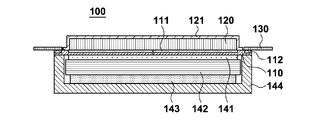
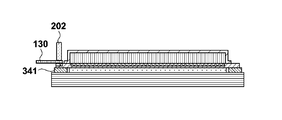
- FIGS. 1A to 1C A configuration example of the radiation detection apparatus 100 according to some embodiments will be described with reference to FIGS. 1A to 1C.
- 1A is a plan view of the radiation detection apparatus 100
- FIG. 1B is a cross-sectional view taken along the line AA ′ of the radiation detection apparatus 100
- FIG. 1C is a cross-sectional view taken along the line BB ′ of the radiation detection apparatus 100. .
- the radiation detection apparatus 100 has the components shown in FIGS. 1A to 1C.
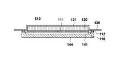
- the sensor panel 110 includes a pixel array 111 and an electrical connection portion 112 on one main surface (the upper surface in FIG. 1B, hereinafter referred to as a front surface).
- a pixel array 111 a plurality of pixels are arranged in an array, and each pixel includes a photoelectric conversion element.
- the electrical connection unit 112 is located outside the pixel array 111 and is electrically connected to the pixel array 111.
- a plurality of electrical connection portions 112 are arranged along two opposing sides of the radiation detection apparatus 100.
- the electrical connection portions 112 may be disposed on two adjacent sides, may be disposed on only one side, or may be disposed on three sides or all sides.
- the sensor panel 110 is configured by a plurality of sensor chips each having the pixel array 111 and the electrical connection portion 112. Around the plurality of sensor chips, a dummy chip 113 having no pixel array 111 and no electrical connection portion 112 is disposed. Instead of this, the sensor panel 110 may be configured by one sensor chip.
- the sensor panel 110 may have any configuration as long as it includes the pixel array 111 and the electrical connection portion 112.
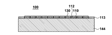
- the sensor panel 110 may be a CMOS sensor or a CCD sensor in which a semiconductor element is formed on a silicon substrate.
- the sensor panel 110 may be a flat panel in which a semiconductor element is formed on a substrate such as glass.
- the radiation detection apparatus 100 may be a front-side irradiation type (a type in which radiation enters from the surface of the sensor panel 110) or a back-side irradiation type (a type in which radiation enters from the back side of the sensor panel).
- the back surface of the sensor panel 110 is a main surface (a lower surface in FIG. 1B) opposite to the front surface of the sensor panel 110.
- imaging is performed using an X-ray having a tube voltage as low as about 25 keV. Therefore, when the radiation detection apparatus 100 is a backside illumination type, a thin substrate may be used to suppress radiation absorption by the substrate of the sensor panel 110, assuming that the radiation detection device 100 is used for mammography.
- Table 1 shows X-rays with a tube voltage of 25 KeV for single crystal silicon substrates of various thicknesses based on the transmittance of a single crystal silicon substrate of 0.775 mm thickness, which is a typical 300 mm wafer thickness. The calculation result of the improvement rate of the transmittance of is shown.
- Table 2 shows the results of calculating the improvement rate of the X-ray transmittance of a tube voltage of 25 KeV with respect to the glass substrate of various thicknesses based on the transmittance of the 0.7 mm-thick glass substrate. .
- the sensor panel 110 may have a protective layer that covers and protects the pixel array 111 on the surface side.
- the protective layer is formed of, for example, an organic resin, and for example, an organic resin having high heat resistance is used.
- organic resins include polyimide resins, styrene resins, epoxy resins, acrylic resins, polyvinylidene chloride resins, polyvinylidene fluoride resins, polyester resins, polyolefin resins, and the like.
- the scintillator layer 120 is disposed on the surface side of the sensor panel 110 at a position that covers the pixel array 111.
- the scintillator layer 120 converts radiation incident on the radiation detection apparatus 100 into light having a wavelength (for example, visible light) that can be detected by the photoelectric conversion element of the pixel array 111.
- the scintillator layer 120 is formed of, for example, an alkali halide material typified by a material (CsI: Tl) in which cesium iodide (hereinafter, CsI) is doped with Tl.
- the scintillator layer 120 is formed of a powder phosphor (hereinafter referred to as GOS) in which a metal oxysulfide (eg, Gd 2 O 2 S) is doped with a trivalent rare earth such as terbium or europium as a light emission center. .
- GOS powder phosphor
- a metal oxysulfide eg, Gd 2 O 2 S
- a trivalent rare earth such as terbium or europium as a light emission center.
- the surface of the scintillator layer 120 other than the surface in contact with the sensor panel 110 may be covered with the scintillator protective layer 121.
- the scintillator protective layer 121 suppresses a decrease in light emission amount and sharpness due to moisture absorption of the scintillator layer 120.
- the scintillator protective layer 121 can be formed by bonding an organic resin having a low moisture permeability or a sheet having a low moisture permeability through an adhesive layer such as an adhesive or a pressure-sensitive adhesive.
- the organic resin having a low moisture permeability include chlorine resins such as polyparaxylylene and polyvinylidene chloride, and fluorine resins such as PCTFE and polyvinylidene fluoride.
- the scintillator protective layer 121 is formed by bonding an aluminum sheet using an adhesive.
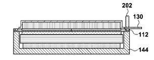
- the wiring member 130 is attached to the electrical connection portion 112.
- the wiring member 130 is, for example, a flexible wiring board (FPC).
- the conductor included in the wiring member 130 is electrically connected to the electrical connection portion 112.
- An external device and the pixel array 111 exchange electrical signals through the wiring member 130 and the electrical connection unit 112.
- the back surface of the sensor panel 110 is bonded to the surface of the support substrate 142 with an adhesive layer 141.
- the adhesive layer 141 is in contact with the portion where the pixel array 111 is disposed on the back surface of the sensor panel 110, but is not in contact with the portion where the electrical connection portion 112 is disposed.
- the support substrate 142 supports the pixel array 111 from the back side of the sensor panel 110.
- a highly heat-resistant member may be used as the support substrate 142.
- a member having a high radiation transmittance may be used as the support substrate 142.
- Such members include light metals such as aluminum, magnesium, aluminum alloys and magnesium alloys, alloys composed of light metals, crystals such as silicon, germanium and carbon, amorphous carbons, glass, ceramics, ceramics, and other amorphous carbon fiber reinforcements.
- light metals such as aluminum, magnesium, aluminum alloys and magnesium alloys, alloys composed of light metals, crystals such as silicon, germanium and carbon, amorphous carbons, glass, ceramics, ceramics, and other amorphous carbon fiber reinforcements.
- composite materials such as plastic (CFRP) and glass fiber reinforced plastic (GFRP), and resins having heat resistance such as aramid resin, polyimide resin, PPS resin, PEEK resin, epoxy resin, and acrylic resin.
- the adhesive layer 141 also functions as a buffer member.
- the back surface of the support substrate 142 is bonded to the bottom of the box-shaped frame 144 by an adhesive layer 143.
- a side wall of the frame body 144 is in contact with a portion of the back surface of the sensor panel 110 where the electrical connection portion 112 is disposed. Therefore, the side wall of the frame body 144 supports the electrical connection portion 112 from the back side of the sensor panel 110.
- the frame body 144 has a higher elastic modulus than the adhesive layer 141.
- the elastic modulus may be, for example, a bulk elastic modulus.
- the compressive strength of the frame 144 is 90 MPa or more (918 kgf / cm 2 or more).
- the frame 144 is made of, for example, metal such as aluminum, aluminum alloy, magnesium, magnesium alloy, iron, stainless steel, crystal such as silicon, germanium, carbon, amorphous such as amorphous carbon, glass, ceramic, CFRP, GFRP And a composite material such as aramid resin, epoxy resin, acrylic resin, polyethylene resin, phenol resin, cellulose acetate resin, and vinyl chloride resin. There is a gap between the side wall of the frame body 144 and the adhesive layer 141.
- the back surface of the sensor panel 110 includes a portion that is not covered by any of them between the frame body 144 and the adhesive layer 141.
- the sensor panel 110 and the support substrate 142 are bonded by an adhesive layer 141, and the frame body 144 and the support substrate 142 are bonded by an adhesive layer 143. Therefore, the frame body 144 is fixed to the sensor panel 110, and the frame body 144 cannot be removed from the radiation detection apparatus 100.
- a sensor panel 110 having a pixel array 111 and an electrical connection portion 112 is prepared. This step may be performed by any method, and an existing method may be used, and thus detailed description is omitted.
- the back surface of the prepared sensor panel 110 may be polished by chemical polishing (etching) or the like to thin the substrate of the sensor panel 110.
- the substrate of the sensor panel 110 may be polished so that the thickness of the substrate becomes 5 mm or less.
- the X-ray transmittance can be improved by 18.5% as compared with the case of a silicon substrate having a thickness of 0.775 mm.
- the thickness of the glass substrate of the sensor panel 110 is set to, for example, 0.3 mm, so that the X-ray transmittance is compared with the case of a 0.7 mm thick glass substrate. Can be improved by 21.8%.
- the adhesive layer 141 is, for example, a silicone pressure-sensitive adhesive having a thickness of 100 ⁇ m.
- the adhesive layer 141 is in contact with the portion where the pixel array 111 is disposed on the back surface of the sensor panel 110, but is not in contact with the portion where the electrical connection portion 112 is disposed.
- the scintillator layer 120 is disposed on the surface side of the sensor panel 110.
- the scintillator layer 120 is formed, for example, by simultaneously heating and evaporating CsI and TlI in a vacuum chamber.
- the resistance heating boat is filled with a phosphor material as an evaporation material, and the sensor panel 110 is installed on a support holder of the evaporation apparatus.
- the inside of the vapor deposition apparatus is evacuated by a vacuum pump, Ar gas is introduced, and the degree of vacuum is adjusted to 0.1 Pa to perform vapor deposition.
- the scintillator layer 120 is formed by applying and drying GOS or the like, for example.
- a scintillator protective layer 121 covering the scintillator layer 120 is formed.
- the scintillator protective layer 121 is formed by laminating an aluminum sheet on which an adhesive is bonded in advance so as to cover the scintillator layer 120 using a roll laminator.
- Polyparaxylylene may be formed by CVD as the scintillator protective layer 121.
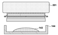
- the sensor panel 110 on which the scintillator layer 120 is formed is placed in a CVD chamber, evacuated to 30 Pa, and then a polyparaxylylene film is formed while rotating the stage on which the sensor panel 110 is placed at 5 rpm. Do. Through the above steps, the structure 200 shown in FIG. 2A is formed.
- an adhesive layer 143 is applied to the bottom of the frame body 144, and the upper side of the structure 200 (upper surface of the scintillator protection layer 121) is vacuum-sucked by the suction stage 201.
- the frame 144 for example, a 2 mm-thick CFRP plate processed into a box shape is used.
- the adhesive layer 143 is formed of, for example, a two-component type epoxy resin that can be cured by mixing two components. By using a two-pack type epoxy resin, the adhesive layer 143 can be cured without heating.
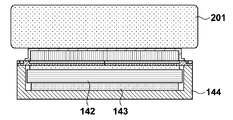
- the structure 200 is attached to the frame 144.
- the structure 200 is pressurized with a pressure of 0.05 MPa, for example. If the pressure at the time of attachment is too high, the sensor panel 110 may break. When the pressure at the time of attachment is too low, the contact between the sensor panel 110 and the frame body 144 becomes insufficient, and the sensor panel 110 may break when the wiring member 130 is attached.
- the wiring member 130 is disposed on the electrical connection portion 112 through an adhesive member such as an anisotropic conductive film (ACF) or a gold bump. Thereafter, the wiring member 130 is thermocompression bonded to the electrical connection portion 112 by the pressure bonding head 202 at a temperature of 100 ° C. to 200 ° C., a pressure of 1 MPa to 5 MPa, and a time of 5 seconds to 5 minutes. In this thermocompression bonding, a part of the sensor panel 110 where the electrical connection portion 112 is disposed is supported by the frame body 144 from the back surface.
- ACF anisotropic conductive film
- the frame body 144 since the frame body 144 has a higher elastic modulus than the adhesive layer 141, the frame body 144 is not easily deformed by the pressure from the crimping head 202. Therefore, deformation of the sensor panel 110 can be suppressed, and the adhesiveness between the electrical connection portion 112 and the wiring member 130 is improved. As a result, the radiation image obtained from the radiation detection apparatus 100 has high quality.
- the wiring member 130 may be bonded to the electrical connection portion 112 by crimping without heating.
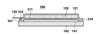
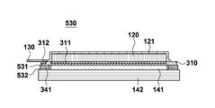
- FIGS. 3A to 3C are plan views of the radiation detection apparatus 300
- FIG. 3B is a cross-sectional view taken along the line AA ′ of the radiation detection apparatus 300
- FIG. 3C is a cross-sectional view taken along the line BB ′ of the radiation detection apparatus 300.
- the radiation detection apparatus 300 includes the components shown in FIGS. 3A to 3C.
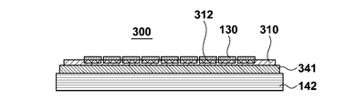
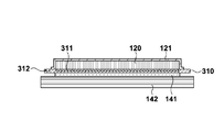
- the sensor panel 310 includes a pixel array 311 and an electrical connection portion 312 on one main surface (the upper surface in FIG. 3B, hereinafter referred to as a front surface). Since the pixel array 311 and the electrical connection unit 312 may be the same as the pixel array 111 and the electrical connection unit 112, description thereof will be omitted.
- the sensor panel 310 is constituted by one sensor chip. However, as in FIGS. 1A to 1C, the sensor panel 310 may be constituted by a plurality of sensor chips.
- a support member 341 is disposed between a portion of the sensor panel 310 where the electrical connection portion 312 is disposed and the support substrate 142. That is, the support member 341 supports the electrical connection portion 312 from the back side of the sensor panel 310.
- the elastic modulus of the support member 341 is larger than the elastic modulus of the adhesive layer 141.
- a material having a compressive strength of 90 MPa or more can be used as the support member 341.
- an organic resin such as an epoxy resin having a compressive strength of 150 MPa may be used.
- a metallic material such as a metal or a metal alloy having a compressive strength of 90 MPa or more may be used.
- the material of the support member 34 stainless steel having a compressive strength of 400 MPa is used.
- a material having adhesiveness may be used as the material of the support member 341. That is, the support member 341 may be an adhesive layer that adheres the back side of the electrical connection portion 312 and the support substrate 142. Further, the material of the support member 341 may have curability such as photocurability and thermosetting.
- the radiation detection apparatus 300 can have the same advantages as the radiation detection apparatus 100. Furthermore, since the radiation detection apparatus 300 has fewer components than the radiation detection apparatus 100, it can be manufactured at low cost.
- a sensor panel 310 having a pixel array 311 and an electrical connection portion 312 is prepared. This step may be performed by any method, and an existing method may be used, and thus detailed description is omitted.
- the sensor panel 310 is bonded to the support substrate 142 with the adhesive layer 141, and the scintillator layer 120 and the scintillator protection layer 121 are formed on the sensor panel 310.
- a support member 341 is inserted between the portion of the sensor panel 310 where the electrical connection portion 312 is disposed and the support substrate 142.
- a dispenser MS-10 manufactured by Musashi Engineering an epoxy resin before curing is placed between the support substrate 142 and the sensor panel 110, and then cured at 80 ° C. for 1 hour.
- the support member 341 is formed.
- the wiring member 130 is crimped to the electrical connection portion 312. Since this process is the same as the process of FIG. 2D, the overlapping description is omitted.
- the support member 341 is disposed after the sensor panel 310 is bonded to the support substrate 142.
- the sensor panel 310 may be bonded to the support substrate 142 after the support member 341 is disposed on the support substrate 142.
- FIGS. 5A to 5C a configuration example of a radiation detection apparatus according to various other embodiments of the present invention will be described with reference to FIGS. 5A to 5C.
- the same elements as those of the radiation detection apparatuses 100 and 300 are denoted by the same reference numerals, and redundant description is omitted.
- the sensor panel 110 is directly bonded to the frame body 144 by the adhesive layer 141.
- a curable adhesive layer 521 is disposed between the frame body 144 and a portion of the back surface of the sensor panel 110 where the electrical connection portion 112 is disposed.
- the back surface of the sensor panel 110 is polished, irregularities such as polishing unevenness and polishing marks by an abrasive may occur on the back surface.
- the unevenness is alleviated by the adhesive layer 521.
- the adhesive layer 521 in a state before being cured is disposed between a portion of the back surface of the sensor panel 110 where the electrical connection portion 112 is disposed and the frame body 144. Thereafter, the adhesive layer 521 is cured.
- the elastic modulus of the adhesive layer 521 after curing is higher than the elastic modulus of the adhesive layer 141.
- the adhesive layer 141 supports the electrical connection portion 112 from the back side of the sensor panel 110.
- a resin such as an epoxy resin, an acrylic resin, a polyethylene resin, a phenol resin, a cellulose acetate resin, or a vinyl chloride resin can be used.
- the support member 341 and the sensor panel 310 are bonded by the adhesive layer 531, and the support member 341 and the support substrate 142 are bonded by the adhesive layer 532. Since both of the adhesive layers 531 and 532 may be the same as the adhesive layer 521, overlapping description is omitted.
- the scintillator layer is formed directly on the sensor panel.
- a scintillator panel having a scintillator layer may be prepared separately from the sensor panel, and the radiation detection apparatus may be formed by superimposing the sensor panel and the scintillator panel.
- the radiation detection apparatus may be a radiation detection apparatus of a type that does not have a scintillator layer and the conversion element of the sensor panel directly converts radiation into electric charges.
- FIG. 6 is a diagram showing an application example of any of the above-described radiation detection apparatuses to an X-ray diagnostic system (radiation detection system).
- X-ray 6060 as radiation generated in the X-ray tube 6050 (radiation source) passes through the chest 6062 of the subject or patient 6061 and enters the detection device 6040 that is one of the above-described radiation detection devices.
- This incident X-ray includes information inside the body of the patient 6061.
- the scintillator emits light in response to the incidence of X-rays, and this is photoelectrically converted to obtain electrical information.
- the radiation detection system includes at least a detection device and a signal processing unit that processes a signal from the detection device.
- This information can be transferred to a remote location by a transmission processing unit such as a telephone line 6090, displayed on a display 6081 serving as a display unit such as a doctor room in another location, or stored in a recording unit such as an optical disc. It is also possible for a doctor to make a diagnosis. Moreover, it can also record on the film 6110 used as a recording medium by the film processor 6100 used as a recording part.
- a transmission processing unit such as a telephone line 6090
- displayed on a display 6081 serving as a display unit such as a doctor room in another location or stored in a recording unit such as an optical disc. It is also possible for a doctor to make a diagnosis.
- it can also record on the film 6110 used as a recording medium by the film processor 6100 used as a recording part.
- CMOS chip is used as the sensor panel 110 in the configuration shown in FIGS. 1A to 1C.
- the back surface of the silicon substrate of the sensor panel 110 is polished until the thickness becomes 0.3 mm.
- a CRFP substrate having a thickness of 1 mm is used as the support substrate 142.
- CsI Tl formed by vacuum deposition is used.
- the scintillator protective layer 121 a film in which an aluminum sheet is bonded is used.
- frame 144 a CFRP substrate impregnated with an epoxy resin is used.
- the adhesive layer 141 a silicone adhesive having a thickness of 100 ⁇ m is used.
- adhesive layer 143 a two-pack type epoxy resin is used.
- a CMOS chip is used as the sensor panel 110 in the configuration shown in FIGS. 3A to 3C.
- the back surface of the silicon substrate of the sensor panel 110 is polished until the thickness becomes 0.3 mm.
- a CRFP substrate having a thickness of 1 mm is used as the support substrate 142.
- CsI Tl formed by vacuum deposition is used.
- the scintillator protective layer 121 a film in which an aluminum sheet is bonded is used.
- an epoxy resin having a compressive strength of 150 MPa is used.
- the adhesive layer 141 a silicone adhesive having a thickness of 100 ⁇ m is used.
- a CMOS chip is used as the sensor panel 110 in the configuration shown in FIGS. 3A to 3C.
- the back surface of the silicon substrate of the sensor panel 110 is polished until the thickness becomes 0.3 mm.
- a CRFP substrate having a thickness of 1 mm is used as the support substrate 142.
- CsI: Tl formed by vacuum deposition is used as the scintillator layer 120.
- the scintillator protective layer 121 a film in which an aluminum sheet is bonded is used.
- the support member 341 stainless steel having a compressive strength of 400 MPa and a thickness of 0.2 mm is used.
- As the adhesive layer 141 a silicone adhesive having a thickness of 200 ⁇ m is used.
- a flat panel is used as the sensor panel 110 in the configuration shown in FIGS. 3A to 3C.
- the back surface of the glass substrate of the sensor panel 110 is polished until the thickness becomes 0.3 mm.
- a CRFP substrate having a thickness of 1 mm is used as the support substrate 142.
- the scintillator layer 120 polyparaxylylene formed by CVD is used.
- the scintillator protective layer 121 a film in which an aluminum sheet is bonded is used.
- an epoxy resin having a compressive strength of 150 MPa is used.
- the adhesive layer 141 a silicone adhesive having a thickness of 100 ⁇ m is used.
Landscapes
- Health & Medical Sciences (AREA)
- Life Sciences & Earth Sciences (AREA)
- Engineering & Computer Science (AREA)
- Medical Informatics (AREA)
- Physics & Mathematics (AREA)
- Pathology (AREA)
- Public Health (AREA)
- Biophysics (AREA)
- Nuclear Medicine, Radiotherapy & Molecular Imaging (AREA)
- Optics & Photonics (AREA)
- Veterinary Medicine (AREA)
- Radiology & Medical Imaging (AREA)
- Biomedical Technology (AREA)
- Heart & Thoracic Surgery (AREA)
- Molecular Biology (AREA)
- Surgery (AREA)
- Animal Behavior & Ethology (AREA)
- General Health & Medical Sciences (AREA)
- High Energy & Nuclear Physics (AREA)
- Mathematical Physics (AREA)
- Computer Vision & Pattern Recognition (AREA)
- Human Computer Interaction (AREA)
- Measurement Of Radiation (AREA)
Priority Applications (1)
| Application Number | Priority Date | Filing Date | Title |
|---|---|---|---|
| US15/053,045 US10283555B2 (en) | 2013-09-06 | 2016-02-25 | Radiation detection apparatus, manufacturing method therefor, and radiation detection system |
Applications Claiming Priority (2)
| Application Number | Priority Date | Filing Date | Title |
|---|---|---|---|
| JP2013185703A JP6310216B2 (ja) | 2013-09-06 | 2013-09-06 | 放射線検出装置及びその製造方法並びに放射線検出システム |
| JP2013-185703 | 2013-09-06 |
Related Child Applications (1)
| Application Number | Title | Priority Date | Filing Date |
|---|---|---|---|
| US15/053,045 Continuation US10283555B2 (en) | 2013-09-06 | 2016-02-25 | Radiation detection apparatus, manufacturing method therefor, and radiation detection system |
Publications (1)
| Publication Number | Publication Date |
|---|---|
| WO2015033506A1 true WO2015033506A1 (ja) | 2015-03-12 |
Family
ID=52628009
Family Applications (1)
| Application Number | Title | Priority Date | Filing Date |
|---|---|---|---|
| PCT/JP2014/003730 Ceased WO2015033506A1 (ja) | 2013-09-06 | 2014-07-15 | 放射線検出装置及びその製造方法並びに放射線検出システム |
Country Status (3)
| Country | Link |
|---|---|
| US (1) | US10283555B2 (enExample) |
| JP (1) | JP6310216B2 (enExample) |
| WO (1) | WO2015033506A1 (enExample) |
Families Citing this family (12)
| Publication number | Priority date | Publication date | Assignee | Title |
|---|---|---|---|---|
| WO2018030140A1 (ja) * | 2016-08-08 | 2018-02-15 | ソニーセミコンダクタソリューションズ株式会社 | 撮像素子、製造方法、および電子機器 |
| JP6778118B2 (ja) | 2017-01-13 | 2020-10-28 | キヤノン株式会社 | 放射線撮像装置及び放射線撮像システム |
| WO2019012846A1 (ja) | 2017-07-10 | 2019-01-17 | キヤノン株式会社 | 放射線撮像装置および放射線撮像システム |
| JP7030478B2 (ja) | 2017-11-09 | 2022-03-07 | キヤノン株式会社 | 撮影台および放射線撮影システム |
| JP7314118B2 (ja) | 2018-03-19 | 2023-07-25 | 富士フイルム株式会社 | 放射線検出器、放射線画像撮影装置及び放射線検出器の製造方法 |
| JP2019174365A (ja) * | 2018-03-29 | 2019-10-10 | シャープ株式会社 | 撮像パネル |
| CN110323235A (zh) * | 2018-03-29 | 2019-10-11 | 夏普株式会社 | 摄像面板 |
| JP6659182B2 (ja) * | 2018-07-23 | 2020-03-04 | キヤノン株式会社 | 放射線撮像装置、その製造方法及び放射線撮像システム |
| JP7185481B2 (ja) * | 2018-10-18 | 2022-12-07 | 浜松ホトニクス株式会社 | 放射線撮像装置 |
| JP7181049B2 (ja) * | 2018-10-18 | 2022-11-30 | 浜松ホトニクス株式会社 | 放射線撮像装置、放射線撮像装置の製造方法、及び放射線撮像装置の修復方法 |
| JP7181050B2 (ja) * | 2018-10-18 | 2022-11-30 | 浜松ホトニクス株式会社 | 放射線撮像装置 |
| JP7289768B2 (ja) * | 2019-10-09 | 2023-06-12 | キヤノン株式会社 | 放射線撮影装置 |
Citations (3)
| Publication number | Priority date | Publication date | Assignee | Title |
|---|---|---|---|---|
| JP2005197729A (ja) * | 1999-06-14 | 2005-07-21 | Sharp Corp | 外部回路実装方法および熱圧着装置 |
| JP2006148005A (ja) * | 2004-11-24 | 2006-06-08 | Canon Inc | 半導体装置、放射線撮像装置、及びその製造方法 |
| JP2008026013A (ja) * | 2006-07-18 | 2008-02-07 | Toshiba Corp | シンチレータパネルおよび放射線検出器 |
Family Cites Families (25)
| Publication number | Priority date | Publication date | Assignee | Title |
|---|---|---|---|---|
| US5952714A (en) * | 1995-08-02 | 1999-09-14 | Matsushita Electronics Corporation | Solid-state image sensing apparatus and manufacturing method thereof |
| AU2001234152A1 (en) * | 2000-02-25 | 2001-09-03 | Hamamatsu Photonics K.K. | X-ray imaging device and method of manufacture thereof |
| JP2002305261A (ja) * | 2001-01-10 | 2002-10-18 | Canon Inc | 電子部品及びその製造方法 |
| JP3519720B2 (ja) * | 2001-06-11 | 2004-04-19 | 松下電器産業株式会社 | 電子デバイス |
| JP2005072978A (ja) * | 2003-08-25 | 2005-03-17 | Renesas Technology Corp | 固体撮像装置およびその製造方法 |
| JP4289913B2 (ja) * | 2003-03-12 | 2009-07-01 | キヤノン株式会社 | 放射線検出装置及びその製造方法 |
| JP2004296656A (ja) * | 2003-03-26 | 2004-10-21 | Canon Inc | 放射線撮像装置 |
| US7355184B2 (en) * | 2003-04-07 | 2008-04-08 | Canon Kabushiki Kaisha | Radiation detecting apparatus and method for manufacturing the same |
| JP4208790B2 (ja) | 2004-08-10 | 2009-01-14 | キヤノン株式会社 | 放射線検出装置の製造方法 |
| US7514686B2 (en) * | 2004-08-10 | 2009-04-07 | Canon Kabushiki Kaisha | Radiation detecting apparatus, scintillator panel, their manufacturing method and radiation detecting system |
| JP4266898B2 (ja) | 2004-08-10 | 2009-05-20 | キヤノン株式会社 | 放射線検出装置とその製造方法および放射線撮像システム |
| JP4464260B2 (ja) | 2004-11-24 | 2010-05-19 | キヤノン株式会社 | 半導体装置、放射線撮像装置、及びその製造方法 |
| JP2007155662A (ja) * | 2005-12-08 | 2007-06-21 | Canon Inc | 放射線検出装置及びそれを用いた放射線撮像システム |
| JP4670855B2 (ja) * | 2007-11-08 | 2011-04-13 | セイコーエプソン株式会社 | 表示装置および時計 |
| JP5607426B2 (ja) | 2010-05-28 | 2014-10-15 | キヤノン株式会社 | 放射線検出装置及び放射線撮像システム |
| JP5562134B2 (ja) | 2010-06-17 | 2014-07-30 | キヤノン株式会社 | 放射線検出装置、その製造方法及び放射線撮像システム |
| JP2012168128A (ja) | 2011-02-16 | 2012-09-06 | Canon Inc | 放射線検出装置及び放射線撮像システム |
| JP5789134B2 (ja) * | 2011-06-16 | 2015-10-07 | 株式会社ジャパンディスプレイ | 照明装置、表示装置及び液晶表示装置 |
| JP5911274B2 (ja) | 2011-11-28 | 2016-04-27 | キヤノン株式会社 | 放射線検出装置及び放射線撮像システム |
| JP6081697B2 (ja) * | 2011-12-07 | 2017-02-15 | 浜松ホトニクス株式会社 | センサユニット及び固体撮像装置 |
| JP2013140036A (ja) | 2011-12-28 | 2013-07-18 | Canon Inc | 放射線検出装置 |
| JP6200171B2 (ja) | 2012-06-04 | 2017-09-20 | キヤノン株式会社 | 放射線検出装置及び撮像システム |
| JP6000680B2 (ja) | 2012-06-20 | 2016-10-05 | キヤノン株式会社 | 放射線検出装置、その製造方法及び撮像システム |
| JP6071283B2 (ja) | 2012-07-04 | 2017-02-01 | キヤノン株式会社 | 放射線検出装置及びその製造方法 |
| JP6092568B2 (ja) | 2012-10-11 | 2017-03-08 | キヤノン株式会社 | 放射線検出装置及び放射線検出システム |
-
2013
- 2013-09-06 JP JP2013185703A patent/JP6310216B2/ja active Active
-
2014
- 2014-07-15 WO PCT/JP2014/003730 patent/WO2015033506A1/ja not_active Ceased
-
2016
- 2016-02-25 US US15/053,045 patent/US10283555B2/en active Active
Patent Citations (3)
| Publication number | Priority date | Publication date | Assignee | Title |
|---|---|---|---|---|
| JP2005197729A (ja) * | 1999-06-14 | 2005-07-21 | Sharp Corp | 外部回路実装方法および熱圧着装置 |
| JP2006148005A (ja) * | 2004-11-24 | 2006-06-08 | Canon Inc | 半導体装置、放射線撮像装置、及びその製造方法 |
| JP2008026013A (ja) * | 2006-07-18 | 2008-02-07 | Toshiba Corp | シンチレータパネルおよび放射線検出器 |
Also Published As
| Publication number | Publication date |
|---|---|
| JP6310216B2 (ja) | 2018-04-11 |
| US20160181308A1 (en) | 2016-06-23 |
| JP2015052535A (ja) | 2015-03-19 |
| US10283555B2 (en) | 2019-05-07 |
Similar Documents
| Publication | Publication Date | Title |
|---|---|---|
| JP6310216B2 (ja) | 放射線検出装置及びその製造方法並びに放射線検出システム | |
| US8648312B2 (en) | Radiation detection apparatus, manufacturing method thereof, and radiation detection system | |
| US9081104B2 (en) | Radiation detection apparatus and radiation detection system | |
| CN102655160B (zh) | 放射线检测装置、闪烁体板、制造方法和放射线检测系统 | |
| JP6100045B2 (ja) | 放射線検出装置、放射線検出システム及び放射線検出装置の製造方法 | |
| CN103515404B (zh) | 放射线检测装置及其制造方法和成像系统 | |
| US9177922B2 (en) | Electric device, method for manufacturing the same, and radiation inspection apparatus | |
| JP4789372B2 (ja) | 放射線検出装置、システム及びそれらに備えられるシンチレータパネル | |
| US20140091225A1 (en) | Radiation imaging apparatus, radiation imaging system, and radiation imaging apparatus manufacturing method | |
| CN103370637A (zh) | 辐射检测设备和辐射检测系统 | |
| JP4464260B2 (ja) | 半導体装置、放射線撮像装置、及びその製造方法 | |
| US10345455B2 (en) | Radiation detection apparatus, radiation imaging system, and method of manufacturing radiation detection apparatus | |
| CN106461794B (zh) | X射线探测器面板 | |
| CN102621574A (zh) | 闪烁体面板、其制造方法和放射线检测设备 | |
| JP2007071836A (ja) | 放射線検出装置及び放射線撮像システム | |
| JP2004061116A (ja) | 放射線検出装置及びシステム | |
| JP2015155799A (ja) | シンチレータ、放射線検出装置、放射線検出装置の製造方法及び放射線検出システム | |
| JP6555955B2 (ja) | 放射線検出装置及び放射線撮像システム | |
| JP7196020B2 (ja) | 放射線検出装置及び放射線撮影システム | |
| JP2023169762A (ja) | 放射線検出器の製造方法、放射線検出器、放射線撮像装置および放射線撮像システム | |
| JP2007057428A (ja) | 放射線検出装置及び放射線撮像システム | |
| JP4819344B2 (ja) | 半導体装置、放射線撮像装置、及びその製造方法 | |
| WO2020166224A1 (ja) | シンチレータプレートの製造方法、シンチレータプレート、放射線検出装置および放射線検出システム | |
| JP2022092707A (ja) | 放射線検出装置の製造方法 | |
| JP2024178814A (ja) | 放射線撮像装置、放射線撮像システムおよび放射線撮像装置の製造方法 |
Legal Events
| Date | Code | Title | Description |
|---|---|---|---|
| 121 | Ep: the epo has been informed by wipo that ep was designated in this application |
Ref document number: 14841813 Country of ref document: EP Kind code of ref document: A1 |
|
| NENP | Non-entry into the national phase |
Ref country code: DE |
|
| 122 | Ep: pct application non-entry in european phase |
Ref document number: 14841813 Country of ref document: EP Kind code of ref document: A1 |