JP4464260B2 - 半導体装置、放射線撮像装置、及びその製造方法 - Google Patents
半導体装置、放射線撮像装置、及びその製造方法 Download PDFInfo
- Publication number
- JP4464260B2 JP4464260B2 JP2004338929A JP2004338929A JP4464260B2 JP 4464260 B2 JP4464260 B2 JP 4464260B2 JP 2004338929 A JP2004338929 A JP 2004338929A JP 2004338929 A JP2004338929 A JP 2004338929A JP 4464260 B2 JP4464260 B2 JP 4464260B2
- Authority
- JP
- Japan
- Prior art keywords
- substrate
- gap
- electrical connection
- electrical
- imaging apparatus
- Prior art date
- Legal status (The legal status is an assumption and is not a legal conclusion. Google has not performed a legal analysis and makes no representation as to the accuracy of the status listed.)
- Expired - Fee Related
Links
- 230000005855 radiation Effects 0.000 title claims description 63
- 238000003384 imaging method Methods 0.000 title claims description 53
- 239000004065 semiconductor Substances 0.000 title claims description 39
- 238000004519 manufacturing process Methods 0.000 title claims description 10
- 239000000758 substrate Substances 0.000 claims description 116
- 239000000853 adhesive Substances 0.000 claims description 25
- 230000001070 adhesive effect Effects 0.000 claims description 25
- 238000006243 chemical reaction Methods 0.000 claims description 14
- 238000000034 method Methods 0.000 claims description 13
- 238000012546 transfer Methods 0.000 claims description 5
- 230000013011 mating Effects 0.000 claims 1
- 239000010408 film Substances 0.000 description 17
- NIXOWILDQLNWCW-UHFFFAOYSA-N acrylic acid group Chemical group C(C=C)(=O)O NIXOWILDQLNWCW-UHFFFAOYSA-N 0.000 description 10
- 239000000463 material Substances 0.000 description 10
- OAICVXFJPJFONN-UHFFFAOYSA-N Phosphorus Chemical compound [P] OAICVXFJPJFONN-UHFFFAOYSA-N 0.000 description 9
- 239000010410 layer Substances 0.000 description 8
- 239000006260 foam Substances 0.000 description 7
- 239000011521 glass Substances 0.000 description 7
- 239000011347 resin Substances 0.000 description 7
- 229920005989 resin Polymers 0.000 description 7
- ZWEHNKRNPOVVGH-UHFFFAOYSA-N 2-Butanone Chemical compound CCC(C)=O ZWEHNKRNPOVVGH-UHFFFAOYSA-N 0.000 description 6
- 229910052751 metal Inorganic materials 0.000 description 6
- 239000002184 metal Substances 0.000 description 6
- 125000006850 spacer group Chemical group 0.000 description 6
- 239000004925 Acrylic resin Substances 0.000 description 5
- 229920000178 Acrylic resin Polymers 0.000 description 5
- 229910021417 amorphous silicon Inorganic materials 0.000 description 5
- 230000000694 effects Effects 0.000 description 5
- 229920000139 polyethylene terephthalate Polymers 0.000 description 5
- 239000005020 polyethylene terephthalate Substances 0.000 description 5
- 239000004820 Pressure-sensitive adhesive Substances 0.000 description 4
- 239000011230 binding agent Substances 0.000 description 4
- 238000010586 diagram Methods 0.000 description 4
- 230000008569 process Effects 0.000 description 4
- 238000012545 processing Methods 0.000 description 4
- 239000010409 thin film Substances 0.000 description 4
- 239000003522 acrylic cement Substances 0.000 description 3
- 239000002585 base Substances 0.000 description 3
- 239000013078 crystal Substances 0.000 description 3
- 238000007689 inspection Methods 0.000 description 3
- 238000002360 preparation method Methods 0.000 description 3
- 230000001681 protective effect Effects 0.000 description 3
- CSCPPACGZOOCGX-UHFFFAOYSA-N Acetone Chemical compound CC(C)=O CSCPPACGZOOCGX-UHFFFAOYSA-N 0.000 description 2
- JOYRKODLDBILNP-UHFFFAOYSA-N Ethyl urethane Chemical compound CCOC(N)=O JOYRKODLDBILNP-UHFFFAOYSA-N 0.000 description 2
- XUIMIQQOPSSXEZ-UHFFFAOYSA-N Silicon Chemical compound [Si] XUIMIQQOPSSXEZ-UHFFFAOYSA-N 0.000 description 2
- 239000004809 Teflon Substances 0.000 description 2
- 229920006362 Teflon® Polymers 0.000 description 2
- 239000003513 alkali Substances 0.000 description 2
- 239000000919 ceramic Substances 0.000 description 2
- 230000007547 defect Effects 0.000 description 2
- 230000002950 deficient Effects 0.000 description 2
- 238000006073 displacement reaction Methods 0.000 description 2
- 239000006261 foam material Substances 0.000 description 2
- 150000004820 halides Chemical class 0.000 description 2
- 238000010438 heat treatment Methods 0.000 description 2
- 238000009434 installation Methods 0.000 description 2
- 239000011159 matrix material Substances 0.000 description 2
- 239000002245 particle Substances 0.000 description 2
- 230000002093 peripheral effect Effects 0.000 description 2
- -1 polyethylene terephthalate Polymers 0.000 description 2
- 239000011241 protective layer Substances 0.000 description 2
- 239000011669 selenium Substances 0.000 description 2
- 229910052710 silicon Inorganic materials 0.000 description 2
- 239000010703 silicon Substances 0.000 description 2
- 229910001220 stainless steel Inorganic materials 0.000 description 2
- 239000010935 stainless steel Substances 0.000 description 2
- RSWGJHLUYNHPMX-UHFFFAOYSA-N Abietic-Saeure Natural products C12CCC(C(C)C)=CC2=CCC2C1(C)CCCC2(C)C(O)=O RSWGJHLUYNHPMX-UHFFFAOYSA-N 0.000 description 1
- CTQNGGLPUBDAKN-UHFFFAOYSA-N O-Xylene Chemical compound CC1=CC=CC=C1C CTQNGGLPUBDAKN-UHFFFAOYSA-N 0.000 description 1
- 239000004698 Polyethylene Substances 0.000 description 1
- 239000004642 Polyimide Substances 0.000 description 1
- KHPCPRHQVVSZAH-HUOMCSJISA-N Rosin Natural products O(C/C=C/c1ccccc1)[C@H]1[C@H](O)[C@@H](O)[C@@H](O)[C@@H](CO)O1 KHPCPRHQVVSZAH-HUOMCSJISA-N 0.000 description 1
- BUGBHKTXTAQXES-UHFFFAOYSA-N Selenium Chemical compound [Se] BUGBHKTXTAQXES-UHFFFAOYSA-N 0.000 description 1
- 229910004298 SiO 2 Inorganic materials 0.000 description 1
- 229910000831 Steel Inorganic materials 0.000 description 1
- 238000010521 absorption reaction Methods 0.000 description 1
- 230000002411 adverse Effects 0.000 description 1
- 229910052782 aluminium Inorganic materials 0.000 description 1
- 229910003481 amorphous carbon Inorganic materials 0.000 description 1
- 230000008901 benefit Effects 0.000 description 1
- 230000005540 biological transmission Effects 0.000 description 1
- NTXGQCSETZTARF-UHFFFAOYSA-N buta-1,3-diene;prop-2-enenitrile Chemical compound C=CC=C.C=CC#N NTXGQCSETZTARF-UHFFFAOYSA-N 0.000 description 1
- XQPRBTXUXXVTKB-UHFFFAOYSA-M caesium iodide Chemical compound [I-].[Cs+] XQPRBTXUXXVTKB-UHFFFAOYSA-M 0.000 description 1
- 230000008859 change Effects 0.000 description 1
- YACLQRRMGMJLJV-UHFFFAOYSA-N chloroprene Chemical compound ClC(=C)C=C YACLQRRMGMJLJV-UHFFFAOYSA-N 0.000 description 1
- 239000011248 coating agent Substances 0.000 description 1
- 230000006378 damage Effects 0.000 description 1
- 230000001066 destructive effect Effects 0.000 description 1
- 238000001514 detection method Methods 0.000 description 1
- 238000003745 diagnosis Methods 0.000 description 1
- HQQADJVZYDDRJT-UHFFFAOYSA-N ethene;prop-1-ene Chemical group C=C.CC=C HQQADJVZYDDRJT-UHFFFAOYSA-N 0.000 description 1
- 230000005669 field effect Effects 0.000 description 1
- 238000005259 measurement Methods 0.000 description 1
- 239000007769 metal material Substances 0.000 description 1
- 238000009659 non-destructive testing Methods 0.000 description 1
- NJPPVKZQTLUDBO-UHFFFAOYSA-N novaluron Chemical compound C1=C(Cl)C(OC(F)(F)C(OC(F)(F)F)F)=CC=C1NC(=O)NC(=O)C1=C(F)C=CC=C1F NJPPVKZQTLUDBO-UHFFFAOYSA-N 0.000 description 1
- 230000003287 optical effect Effects 0.000 description 1
- 238000002161 passivation Methods 0.000 description 1
- 229920000728 polyester Polymers 0.000 description 1
- 229920000573 polyethylene Polymers 0.000 description 1
- 229920001721 polyimide Polymers 0.000 description 1
- 229920000098 polyolefin Polymers 0.000 description 1
- 150000003097 polyterpenes Chemical class 0.000 description 1
- 239000000843 powder Substances 0.000 description 1
- 238000002601 radiography Methods 0.000 description 1
- 230000009467 reduction Effects 0.000 description 1
- 230000004044 response Effects 0.000 description 1
- 238000012216 screening Methods 0.000 description 1
- 229910052711 selenium Inorganic materials 0.000 description 1
- 230000001568 sexual effect Effects 0.000 description 1
- 230000035939 shock Effects 0.000 description 1
- 239000002904 solvent Substances 0.000 description 1
- 238000001179 sorption measurement Methods 0.000 description 1
- 239000010959 steel Substances 0.000 description 1
- 230000001629 suppression Effects 0.000 description 1
- 229910052716 thallium Inorganic materials 0.000 description 1
- BKVIYDNLLOSFOA-UHFFFAOYSA-N thallium Chemical compound [Tl] BKVIYDNLLOSFOA-UHFFFAOYSA-N 0.000 description 1
- KHPCPRHQVVSZAH-UHFFFAOYSA-N trans-cinnamyl beta-D-glucopyranoside Natural products OC1C(O)C(O)C(CO)OC1OCC=CC1=CC=CC=C1 KHPCPRHQVVSZAH-UHFFFAOYSA-N 0.000 description 1
- 238000007740 vapor deposition Methods 0.000 description 1
- 239000008096 xylene Substances 0.000 description 1
Images


Classifications
-
- H—ELECTRICITY
- H01—ELECTRIC ELEMENTS
- H01L—SEMICONDUCTOR DEVICES NOT COVERED BY CLASS H10
- H01L27/00—Devices consisting of a plurality of semiconductor or other solid-state components formed in or on a common substrate
- H01L27/14—Devices consisting of a plurality of semiconductor or other solid-state components formed in or on a common substrate including semiconductor components sensitive to infrared radiation, light, electromagnetic radiation of shorter wavelength or corpuscular radiation and specially adapted either for the conversion of the energy of such radiation into electrical energy or for the control of electrical energy by such radiation
- H01L27/144—Devices controlled by radiation
- H01L27/146—Imager structures
- H01L27/14601—Structural or functional details thereof
- H01L27/14618—Containers
-
- H—ELECTRICITY
- H01—ELECTRIC ELEMENTS
- H01L—SEMICONDUCTOR DEVICES NOT COVERED BY CLASS H10
- H01L27/00—Devices consisting of a plurality of semiconductor or other solid-state components formed in or on a common substrate
- H01L27/14—Devices consisting of a plurality of semiconductor or other solid-state components formed in or on a common substrate including semiconductor components sensitive to infrared radiation, light, electromagnetic radiation of shorter wavelength or corpuscular radiation and specially adapted either for the conversion of the energy of such radiation into electrical energy or for the control of electrical energy by such radiation
- H01L27/144—Devices controlled by radiation
- H01L27/146—Imager structures
- H01L27/14643—Photodiode arrays; MOS imagers
- H01L27/14658—X-ray, gamma-ray or corpuscular radiation imagers
- H01L27/14663—Indirect radiation imagers, e.g. using luminescent members
-
- H—ELECTRICITY
- H05—ELECTRIC TECHNIQUES NOT OTHERWISE PROVIDED FOR
- H05K—PRINTED CIRCUITS; CASINGS OR CONSTRUCTIONAL DETAILS OF ELECTRIC APPARATUS; MANUFACTURE OF ASSEMBLAGES OF ELECTRICAL COMPONENTS
- H05K3/00—Apparatus or processes for manufacturing printed circuits
- H05K3/36—Assembling printed circuits with other printed circuits
- H05K3/361—Assembling flexible printed circuits with other printed circuits
-
- H—ELECTRICITY
- H01—ELECTRIC ELEMENTS
- H01L—SEMICONDUCTOR DEVICES NOT COVERED BY CLASS H10
- H01L2924/00—Indexing scheme for arrangements or methods for connecting or disconnecting semiconductor or solid-state bodies as covered by H01L24/00
- H01L2924/0001—Technical content checked by a classifier
- H01L2924/0002—Not covered by any one of groups H01L24/00, H01L24/00 and H01L2224/00
-
- H—ELECTRICITY
- H05—ELECTRIC TECHNIQUES NOT OTHERWISE PROVIDED FOR
- H05K—PRINTED CIRCUITS; CASINGS OR CONSTRUCTIONAL DETAILS OF ELECTRIC APPARATUS; MANUFACTURE OF ASSEMBLAGES OF ELECTRICAL COMPONENTS
- H05K2201/00—Indexing scheme relating to printed circuits covered by H05K1/00
- H05K2201/01—Dielectrics
- H05K2201/0104—Properties and characteristics in general
- H05K2201/0133—Elastomeric or compliant polymer
-
- H—ELECTRICITY
- H05—ELECTRIC TECHNIQUES NOT OTHERWISE PROVIDED FOR
- H05K—PRINTED CIRCUITS; CASINGS OR CONSTRUCTIONAL DETAILS OF ELECTRIC APPARATUS; MANUFACTURE OF ASSEMBLAGES OF ELECTRICAL COMPONENTS
- H05K2201/00—Indexing scheme relating to printed circuits covered by H05K1/00
- H05K2201/10—Details of components or other objects attached to or integrated in a printed circuit board
- H05K2201/10613—Details of electrical connections of non-printed components, e.g. special leads
- H05K2201/10621—Components characterised by their electrical contacts
- H05K2201/10681—Tape Carrier Package [TCP]; Flexible sheet connector
-
- H—ELECTRICITY
- H05—ELECTRIC TECHNIQUES NOT OTHERWISE PROVIDED FOR
- H05K—PRINTED CIRCUITS; CASINGS OR CONSTRUCTIONAL DETAILS OF ELECTRIC APPARATUS; MANUFACTURE OF ASSEMBLAGES OF ELECTRICAL COMPONENTS
- H05K2201/00—Indexing scheme relating to printed circuits covered by H05K1/00
- H05K2201/20—Details of printed circuits not provided for in H05K2201/01 - H05K2201/10
- H05K2201/2036—Permanent spacer or stand-off in a printed circuit or printed circuit assembly
-
- H—ELECTRICITY
- H05—ELECTRIC TECHNIQUES NOT OTHERWISE PROVIDED FOR
- H05K—PRINTED CIRCUITS; CASINGS OR CONSTRUCTIONAL DETAILS OF ELECTRIC APPARATUS; MANUFACTURE OF ASSEMBLAGES OF ELECTRICAL COMPONENTS
- H05K3/00—Apparatus or processes for manufacturing printed circuits
- H05K3/0058—Laminating printed circuit boards onto other substrates, e.g. metallic substrates
-
- H—ELECTRICITY
- H05—ELECTRIC TECHNIQUES NOT OTHERWISE PROVIDED FOR
- H05K—PRINTED CIRCUITS; CASINGS OR CONSTRUCTIONAL DETAILS OF ELECTRIC APPARATUS; MANUFACTURE OF ASSEMBLAGES OF ELECTRICAL COMPONENTS
- H05K3/00—Apparatus or processes for manufacturing printed circuits
- H05K3/22—Secondary treatment of printed circuits
- H05K3/225—Correcting or repairing of printed circuits
Landscapes
- Engineering & Computer Science (AREA)
- Physics & Mathematics (AREA)
- Power Engineering (AREA)
- Microelectronics & Electronic Packaging (AREA)
- Electromagnetism (AREA)
- Condensed Matter Physics & Semiconductors (AREA)
- General Physics & Mathematics (AREA)
- Computer Hardware Design (AREA)
- Health & Medical Sciences (AREA)
- Toxicology (AREA)
- Manufacturing & Machinery (AREA)
- Measurement Of Radiation (AREA)
- Transforming Light Signals Into Electric Signals (AREA)
- Light Receiving Elements (AREA)
- Solid State Image Pick-Up Elements (AREA)
Description
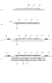
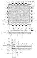
本実施例は、図1〜3に示される放射線撮像装置の例である。
本実施例は、図4(A)〜(C)に示される放射線撮像装置の例である。
以下に、本発明による放射線撮像装置のX線診断システムへの応用例を説明する。図5に、本発明による放射線撮像装置のX線診断システムへの応用例を示す。
10 センサーパネル
20 放射線撮像パネル
100 基板
101 基板の接続電極
110 画素部
150,160 電気部品
161 電気部品の接続電極
180 導電性接着剤
200 シンチレータ
250 接着剤
300 支持部材
350 貼り合わせ部材
501 プレス部材
502 バックアップ
503 ヒーター
505 テフロン(登録商標)シート
510 剛性部材
Claims (11)
- 複数の半導体素子と、該半導体素子の周辺に配され、前記半導体素子に配線を介して電気的に接続された電気接続部と、を有する基板と、
該電気接続部に電気的に接続された電気部品と、
前記基板の前記半導体素子を有する面とは反対側に配され、前記基板と貼り合わせ部材を介して固定された、前記基板を支持する支持部材と、を有する半導体装置において、
少なくとも前記電気接続部を含む領域の前記基板と前記支持部材との間に間隙を有し、
該間隙に配された緩衝部材を有し、該緩衝部材は、前記基板、前記支持部材及び前記貼り合わせ部材とは非接着であることを特徴とする半導体装置。 - 前記緩衝部材は、非接着性の弾性体であることを特徴とする請求項1に記載の半導体装置。
- 放射線又は光を電気信号に変換する変換素子を有する複数の画素が配された画素部と、該画素部の周辺に配され前記画素部に配線を介して電気的に接続された電気接続部と、を有する基板と、
該電気接続部に電気的に接続された電気部品と、
前記基板の前記画素部を有する面とは反対側に配され、前記基板と貼り合わせ部材を介して固定された、前記基板を支持する支持部材と、を有する放射線撮像装置において、
少なくとも前記電気接続部を含む領域の前記基板と前記支持部材との間に間隙を有し、
該間隙に配された緩衝部材を有し、該緩衝部材は、前記基板、前記支持部材及び前記貼り合わせ部材とは非接着であることを特徴とする放射線撮像装置。 - 前記緩衝部材は、非接着性の弾性体であることを特徴とする請求項3に記載の放射線撮像装置。
- 前記変換素子は、光電変換素子であり、
前記画素は、信号転送素子を更に有し、
前記画素の上に配された、放射線を光に変換する波長変換体を有することを特徴とする請求項3または4に記載の放射線撮像装置。 - 前記信号転送素子がスイッチ素子であることを特徴とする請求項5に記載の放射線撮像装置。
- 前記電気部品は、導電性接着剤を介して前記電気接続部に接続されていることを特徴とする請求項3〜6のいずれか1項に記載の放射線撮像装置。
- 前記画素部の周辺に複数の前記電気部品が配置され、
前記間隙は、前記複数の前記電気部品の領域にわたって一括して配置され、前記緩衝部材は、前記複数の前記電気部品に対して1つの前記緩衝部材が前記間隙に配置されていることを特徴とする請求項3〜7のいずれか1項に記載の放射線撮像装置。 - 前記緩衝部材は、1つの前記電気部品に応じて前記間隙に配置されていることを特徴とする請求項3〜7のいずれか1項に記載の放射線撮像装置。
- 複数の半導体素子を含む基板の上に、前記半導体素子の周辺に配された、前記半導体素子に配線を介して電気的に接続された電気接続部を介して電気部品を接続する工程と、
前記基板と支持部材とを、少なくとも前記電気部品が接続された前記電気接続部を含む領域の前記基板と前記支持部材との間に間隙を有するよう貼り合わせ部材を配して固定する工程と、
前記間隙に緩衝部材を配する工程と、
を有する半導体装置の製造方法。 - 複数の半導体素子と、該半導体素子の周辺に配され該半導体素子に電気的に接続された電気接続部と、を有する基板と、該電気接続部に接続された電気部品と、前記基板と貼り合わせ部材を介して固定された支持部材と、少なくとも前記電気部品が接続された前記電気接続部を含む領域の前記基板と前記支持部材との間に設けられた間隙に配された緩衝部材と、を有する半導体装置の製造方法であって、
前記電気接続部から前記電気部品を取り外す工程と、
前記間隙から前記緩衝部材を取り外し、前記緩衝部材が取り外された前記間隙に剛性部材を配置する工程と、
該剛性部材を配置した後に、前記電気接続部に新たな電気部品を接続する工程と、
前記剛性部材を前記間隙から取り外し、前記剛性部材が取り外された前記間隙に緩衝部材を配置する工程と、
を有することを特徴とする半導体装置の製造方法。
Priority Applications (2)
| Application Number | Priority Date | Filing Date | Title |
|---|---|---|---|
| JP2004338929A JP4464260B2 (ja) | 2004-11-24 | 2004-11-24 | 半導体装置、放射線撮像装置、及びその製造方法 |
| US11/286,389 US7564112B2 (en) | 2004-11-24 | 2005-11-25 | Semiconductor device, radiographic imaging apparatus, and method for manufacturing the same |
Applications Claiming Priority (1)
| Application Number | Priority Date | Filing Date | Title |
|---|---|---|---|
| JP2004338929A JP4464260B2 (ja) | 2004-11-24 | 2004-11-24 | 半導体装置、放射線撮像装置、及びその製造方法 |
Publications (3)
| Publication Number | Publication Date |
|---|---|
| JP2006145469A JP2006145469A (ja) | 2006-06-08 |
| JP2006145469A5 JP2006145469A5 (ja) | 2008-01-10 |
| JP4464260B2 true JP4464260B2 (ja) | 2010-05-19 |
Family
ID=36460193
Family Applications (1)
| Application Number | Title | Priority Date | Filing Date |
|---|---|---|---|
| JP2004338929A Expired - Fee Related JP4464260B2 (ja) | 2004-11-24 | 2004-11-24 | 半導体装置、放射線撮像装置、及びその製造方法 |
Country Status (2)
| Country | Link |
|---|---|
| US (1) | US7564112B2 (ja) |
| JP (1) | JP4464260B2 (ja) |
Cited By (1)
| Publication number | Priority date | Publication date | Assignee | Title |
|---|---|---|---|---|
| US10283555B2 (en) | 2013-09-06 | 2019-05-07 | Canon Kabushiki Kaisha | Radiation detection apparatus, manufacturing method therefor, and radiation detection system |
Families Citing this family (18)
| Publication number | Priority date | Publication date | Assignee | Title |
|---|---|---|---|---|
| EP1300694B1 (en) * | 2000-05-19 | 2011-03-23 | Hamamatsu Photonics K.K. | Radiation detector and method of manufacture thereof |
| US7396159B2 (en) * | 2006-06-07 | 2008-07-08 | General Electric Company | X-ray detector panel methods and apparatus |
| DE102006038969B4 (de) * | 2006-08-21 | 2013-02-28 | Siemens Aktiengesellschaft | Röntgenkonverterelement und Verfahren zu dessen Herstellung |
| JP5004848B2 (ja) * | 2007-04-18 | 2012-08-22 | キヤノン株式会社 | 放射線検出装置及び放射線検出システム |
| US7495227B2 (en) * | 2007-07-10 | 2009-02-24 | General Electric Company | Digital x-ray detectors |
| US8399842B2 (en) * | 2009-12-07 | 2013-03-19 | Carestream Health, Inc. | Digital radiographic detector with bonded phosphor layer |
| JP5178900B2 (ja) * | 2010-11-08 | 2013-04-10 | 富士フイルム株式会社 | 放射線検出器 |
| JP2012177624A (ja) * | 2011-02-25 | 2012-09-13 | Fujifilm Corp | 放射線画像検出装置及び放射線画像検出装置の製造方法 |
| JP5788738B2 (ja) * | 2011-08-26 | 2015-10-07 | 富士フイルム株式会社 | 放射線検出器の製造方法 |
| US9450200B2 (en) * | 2012-11-20 | 2016-09-20 | Samsung Display Co., Ltd. | Organic light emitting diode |
| JP6314984B2 (ja) * | 2013-07-04 | 2018-04-25 | コニカミノルタ株式会社 | シンチレータパネル及びその製造方法 |
| US11411041B2 (en) * | 2016-05-16 | 2022-08-09 | Carestream Health, Inc. | Flexible substrate module and fabrication method |
| CN108012442A (zh) * | 2017-12-29 | 2018-05-08 | 广东欧珀移动通信有限公司 | 一种支架 |
| JP7181050B2 (ja) * | 2018-10-18 | 2022-11-30 | 浜松ホトニクス株式会社 | 放射線撮像装置 |
| JP7185481B2 (ja) * | 2018-10-18 | 2022-12-07 | 浜松ホトニクス株式会社 | 放射線撮像装置 |
| JP7181049B2 (ja) * | 2018-10-18 | 2022-11-30 | 浜松ホトニクス株式会社 | 放射線撮像装置、放射線撮像装置の製造方法、及び放射線撮像装置の修復方法 |
| JP2020088066A (ja) * | 2018-11-20 | 2020-06-04 | キヤノン株式会社 | 電子部品および機器 |
| CN113263236B (zh) * | 2021-04-29 | 2023-03-21 | 四川航天燎原科技有限公司 | 一种插针网格阵列封装元器件pga解焊工艺方法 |
Family Cites Families (4)
| Publication number | Priority date | Publication date | Assignee | Title |
|---|---|---|---|---|
| JP3486515B2 (ja) * | 1996-12-13 | 2004-01-13 | キヤノン株式会社 | ガラス基板保持構造及び放射線撮影装置 |
| JP4497663B2 (ja) * | 2000-06-09 | 2010-07-07 | キヤノン株式会社 | 放射線画像撮影装置 |
| JP2002014168A (ja) * | 2000-06-27 | 2002-01-18 | Canon Inc | X線撮像装置 |
| FR2835651B1 (fr) * | 2002-02-06 | 2005-04-15 | St Microelectronics Sa | Dispositif de montage d'un boitier semi-conducteur sur une plaque-support par l'intermediaire d'une embase |
-
2004
- 2004-11-24 JP JP2004338929A patent/JP4464260B2/ja not_active Expired - Fee Related
-
2005
- 2005-11-25 US US11/286,389 patent/US7564112B2/en not_active Expired - Fee Related
Cited By (1)
| Publication number | Priority date | Publication date | Assignee | Title |
|---|---|---|---|---|
| US10283555B2 (en) | 2013-09-06 | 2019-05-07 | Canon Kabushiki Kaisha | Radiation detection apparatus, manufacturing method therefor, and radiation detection system |
Also Published As
| Publication number | Publication date |
|---|---|
| JP2006145469A (ja) | 2006-06-08 |
| US7564112B2 (en) | 2009-07-21 |
| US20060108683A1 (en) | 2006-05-25 |
Similar Documents
| Publication | Publication Date | Title |
|---|---|---|
| US7564112B2 (en) | Semiconductor device, radiographic imaging apparatus, and method for manufacturing the same | |
| JP5693173B2 (ja) | 放射線検出装置及び放射線検出システム | |
| US8648312B2 (en) | Radiation detection apparatus, manufacturing method thereof, and radiation detection system | |
| JP6310216B2 (ja) | 放射線検出装置及びその製造方法並びに放射線検出システム | |
| JP2009133837A (ja) | 放射線検出装置の製造方法、放射線検出装置及び放射線撮像システム | |
| JP2007071836A (ja) | 放射線検出装置及び放射線撮像システム | |
| JP5536527B2 (ja) | 放射線画像撮影装置及び放射線画像撮影システム | |
| CN109324341B (zh) | 放射线检测装置及其制造方法和放射线成像系统 | |
| JP5403848B2 (ja) | 放射線検出装置及び放射線検出システム | |
| KR101818874B1 (ko) | 방사선 검출 장치, 방사선 검출 시스템 및 방사선 검출 장치의 제조 방법 | |
| JP4352964B2 (ja) | 二次元像検出器 | |
| JP5421849B2 (ja) | 放射線画像撮影装置及び放射線画像撮影システム | |
| JP4819344B2 (ja) | 半導体装置、放射線撮像装置、及びその製造方法 | |
| JP2007057428A (ja) | 放射線検出装置及び放射線撮像システム | |
| JP2004061116A (ja) | 放射線検出装置及びシステム | |
| EP3625827B1 (en) | Flexible substrate module and fabrication method | |
| US20200161366A1 (en) | Flexible substrate module and fabrication method | |
| JP2006343277A (ja) | 放射線検出装置及び放射線撮像システム | |
| JP2021056092A (ja) | 放射線撮像装置 | |
| JP2022092707A (ja) | 放射線検出装置の製造方法 | |
| JP7314019B2 (ja) | 放射線検出装置の製造方法 | |
| JP2017223632A (ja) | 放射線検出装置及びその製造方法 | |
| JP6328179B2 (ja) | 放射線検出装置、放射線検出システム、及び、放射線検出装置の製造方法 | |
| JP2022092706A (ja) | 放射線検出装置の製造方法 | |
| JP2023169762A (ja) | 放射線検出器の製造方法、放射線検出器、放射線撮像装置および放射線撮像システム |
Legal Events
| Date | Code | Title | Description |
|---|---|---|---|
| A521 | Request for written amendment filed |
Free format text: JAPANESE INTERMEDIATE CODE: A523 Effective date: 20071116 |
|
| A621 | Written request for application examination |
Free format text: JAPANESE INTERMEDIATE CODE: A621 Effective date: 20071116 |
|
| A131 | Notification of reasons for refusal |
Free format text: JAPANESE INTERMEDIATE CODE: A131 Effective date: 20100105 |
|
| A521 | Request for written amendment filed |
Free format text: JAPANESE INTERMEDIATE CODE: A523 Effective date: 20100126 |
|
| TRDD | Decision of grant or rejection written | ||
| RD04 | Notification of resignation of power of attorney |
Free format text: JAPANESE INTERMEDIATE CODE: A7424 Effective date: 20100201 |
|
| A01 | Written decision to grant a patent or to grant a registration (utility model) |
Free format text: JAPANESE INTERMEDIATE CODE: A01 Effective date: 20100209 |
|
| A01 | Written decision to grant a patent or to grant a registration (utility model) |
Free format text: JAPANESE INTERMEDIATE CODE: A01 |
|
| A61 | First payment of annual fees (during grant procedure) |
Free format text: JAPANESE INTERMEDIATE CODE: A61 Effective date: 20100218 |
|
| FPAY | Renewal fee payment (event date is renewal date of database) |
Free format text: PAYMENT UNTIL: 20130226 Year of fee payment: 3 |
|
| R150 | Certificate of patent or registration of utility model |
Free format text: JAPANESE INTERMEDIATE CODE: R150 |
|
| FPAY | Renewal fee payment (event date is renewal date of database) |
Free format text: PAYMENT UNTIL: 20140226 Year of fee payment: 4 |
|
| LAPS | Cancellation because of no payment of annual fees |