WO2012169053A1 - 半導体装置および半導体装置の製造方法 - Google Patents
半導体装置および半導体装置の製造方法 Download PDFInfo
- Publication number
- WO2012169053A1 WO2012169053A1 PCT/JP2011/063280 JP2011063280W WO2012169053A1 WO 2012169053 A1 WO2012169053 A1 WO 2012169053A1 JP 2011063280 W JP2011063280 W JP 2011063280W WO 2012169053 A1 WO2012169053 A1 WO 2012169053A1
- Authority
- WO
- WIPO (PCT)
- Prior art keywords
- element region
- layer
- region
- semiconductor device
- electrode
- Prior art date
- Legal status (The legal status is an assumption and is not a legal conclusion. Google has not performed a legal analysis and makes no representation as to the accuracy of the status listed.)
- Ceased
Links
Images




Classifications
-
- H—ELECTRICITY
- H10—SEMICONDUCTOR DEVICES; ELECTRIC SOLID-STATE DEVICES NOT OTHERWISE PROVIDED FOR
- H10D—INORGANIC ELECTRIC SEMICONDUCTOR DEVICES
- H10D62/00—Semiconductor bodies, or regions thereof, of devices having potential barriers
- H10D62/10—Shapes, relative sizes or dispositions of the regions of the semiconductor bodies; Shapes of the semiconductor bodies
- H10D62/102—Constructional design considerations for preventing surface leakage or controlling electric field concentration
- H10D62/103—Constructional design considerations for preventing surface leakage or controlling electric field concentration for increasing or controlling the breakdown voltage of reverse-biased devices
- H10D62/105—Constructional design considerations for preventing surface leakage or controlling electric field concentration for increasing or controlling the breakdown voltage of reverse-biased devices by having particular doping profiles, shapes or arrangements of PN junctions; by having supplementary regions, e.g. junction termination extension [JTE]
-
- H—ELECTRICITY
- H10—SEMICONDUCTOR DEVICES; ELECTRIC SOLID-STATE DEVICES NOT OTHERWISE PROVIDED FOR
- H10D—INORGANIC ELECTRIC SEMICONDUCTOR DEVICES
- H10D12/00—Bipolar devices controlled by the field effect, e.g. insulated-gate bipolar transistors [IGBT]
- H10D12/01—Manufacture or treatment
- H10D12/031—Manufacture or treatment of IGBTs
- H10D12/032—Manufacture or treatment of IGBTs of vertical IGBTs
- H10D12/038—Manufacture or treatment of IGBTs of vertical IGBTs having a recessed gate, e.g. trench-gate IGBTs
-
- H—ELECTRICITY
- H10—SEMICONDUCTOR DEVICES; ELECTRIC SOLID-STATE DEVICES NOT OTHERWISE PROVIDED FOR
- H10D—INORGANIC ELECTRIC SEMICONDUCTOR DEVICES
- H10D12/00—Bipolar devices controlled by the field effect, e.g. insulated-gate bipolar transistors [IGBT]
- H10D12/411—Insulated-gate bipolar transistors [IGBT]
- H10D12/441—Vertical IGBTs
- H10D12/461—Vertical IGBTs having non-planar surfaces, e.g. having trenches, recesses or pillars in the surfaces of the emitter, base or collector regions
- H10D12/481—Vertical IGBTs having non-planar surfaces, e.g. having trenches, recesses or pillars in the surfaces of the emitter, base or collector regions having gate structures on slanted surfaces, on vertical surfaces, or in grooves, e.g. trench gate IGBTs
-
- H—ELECTRICITY
- H10—SEMICONDUCTOR DEVICES; ELECTRIC SOLID-STATE DEVICES NOT OTHERWISE PROVIDED FOR
- H10D—INORGANIC ELECTRIC SEMICONDUCTOR DEVICES
- H10D62/00—Semiconductor bodies, or regions thereof, of devices having potential barriers
- H10D62/10—Shapes, relative sizes or dispositions of the regions of the semiconductor bodies; Shapes of the semiconductor bodies
- H10D62/124—Shapes, relative sizes or dispositions of the regions of semiconductor bodies or of junctions between the regions
-
- H—ELECTRICITY
- H10—SEMICONDUCTOR DEVICES; ELECTRIC SOLID-STATE DEVICES NOT OTHERWISE PROVIDED FOR
- H10D—INORGANIC ELECTRIC SEMICONDUCTOR DEVICES
- H10D62/00—Semiconductor bodies, or regions thereof, of devices having potential barriers
- H10D62/10—Shapes, relative sizes or dispositions of the regions of the semiconductor bodies; Shapes of the semiconductor bodies
- H10D62/13—Semiconductor regions connected to electrodes carrying current to be rectified, amplified or switched, e.g. source or drain regions
- H10D62/141—Anode or cathode regions of thyristors; Collector or emitter regions of gated bipolar-mode devices, e.g. of IGBTs
- H10D62/142—Anode regions of thyristors or collector regions of gated bipolar-mode devices
-
- H—ELECTRICITY
- H10—SEMICONDUCTOR DEVICES; ELECTRIC SOLID-STATE DEVICES NOT OTHERWISE PROVIDED FOR
- H10D—INORGANIC ELECTRIC SEMICONDUCTOR DEVICES
- H10D62/00—Semiconductor bodies, or regions thereof, of devices having potential barriers
- H10D62/10—Shapes, relative sizes or dispositions of the regions of the semiconductor bodies; Shapes of the semiconductor bodies
- H10D62/17—Semiconductor regions connected to electrodes not carrying current to be rectified, amplified or switched, e.g. channel regions
- H10D62/393—Body regions of DMOS transistors or IGBTs
-
- H—ELECTRICITY
- H10—SEMICONDUCTOR DEVICES; ELECTRIC SOLID-STATE DEVICES NOT OTHERWISE PROVIDED FOR
- H10D—INORGANIC ELECTRIC SEMICONDUCTOR DEVICES
- H10D62/00—Semiconductor bodies, or regions thereof, of devices having potential barriers
- H10D62/50—Physical imperfections
- H10D62/53—Physical imperfections the imperfections being within the semiconductor body
-
- H—ELECTRICITY
- H10—SEMICONDUCTOR DEVICES; ELECTRIC SOLID-STATE DEVICES NOT OTHERWISE PROVIDED FOR
- H10D—INORGANIC ELECTRIC SEMICONDUCTOR DEVICES
- H10D8/00—Diodes
-
- H—ELECTRICITY
- H10—SEMICONDUCTOR DEVICES; ELECTRIC SOLID-STATE DEVICES NOT OTHERWISE PROVIDED FOR
- H10D—INORGANIC ELECTRIC SEMICONDUCTOR DEVICES
- H10D84/00—Integrated devices formed in or on semiconductor substrates that comprise only semiconducting layers, e.g. on Si wafers or on GaAs-on-Si wafers
- H10D84/60—Integrated devices formed in or on semiconductor substrates that comprise only semiconducting layers, e.g. on Si wafers or on GaAs-on-Si wafers characterised by the integration of at least one component covered by groups H10D10/00 or H10D18/00, e.g. integration of BJTs
- H10D84/611—Combinations of BJTs and one or more of diodes, resistors or capacitors
- H10D84/613—Combinations of vertical BJTs and one or more of diodes, resistors or capacitors
- H10D84/617—Combinations of vertical BJTs and only diodes
-
- H—ELECTRICITY
- H10—SEMICONDUCTOR DEVICES; ELECTRIC SOLID-STATE DEVICES NOT OTHERWISE PROVIDED FOR
- H10P—GENERIC PROCESSES OR APPARATUS FOR THE MANUFACTURE OR TREATMENT OF DEVICES COVERED BY CLASS H10
- H10P32/00—Diffusion of dopants within, into or out of wafers, substrates or parts of devices
- H10P32/10—Diffusion of dopants within, into or out of semiconductor bodies or layers
- H10P32/17—Diffusion of dopants within, into or out of semiconductor bodies or layers characterised by the semiconductor material
- H10P32/171—Diffusion of dopants within, into or out of semiconductor bodies or layers characterised by the semiconductor material being group IV material
-
- H—ELECTRICITY
- H10—SEMICONDUCTOR DEVICES; ELECTRIC SOLID-STATE DEVICES NOT OTHERWISE PROVIDED FOR
- H10P—GENERIC PROCESSES OR APPARATUS FOR THE MANUFACTURE OR TREATMENT OF DEVICES COVERED BY CLASS H10
- H10P32/00—Diffusion of dopants within, into or out of wafers, substrates or parts of devices
- H10P32/10—Diffusion of dopants within, into or out of semiconductor bodies or layers
- H10P32/18—Diffusion lifetime killers
Definitions
- the present application relates to a reverse conduction type semiconductor device in which an IGBT element region and a diode element region are mixed on the same semiconductor substrate.
- Japanese Patent Application Laid-Open No. 2008-192737 discloses a semiconductor device in which IGBT (insulated gate bipolar transistor) and FWD (free wheel diode) are mixed on the same semiconductor substrate.
- IGBT insulated gate bipolar transistor
- FWD free wheel diode
- This semiconductor device by selectively irradiating the FWD region with ions, a defect region having more crystal defects than other regions is formed only in the FWD region.
- the defect area functions as an area (lifetime control area) in which the lifetime of the carrier can be controlled.
- ion irradiation makes it difficult to control the distribution of crystal defects with high accuracy because it is difficult to control the range and distribution of irradiated ions.
- a method of selectively irradiating ions in the FWD region a method of forming an irradiation mask in which an opening is previously formed in a portion corresponding to the FWD region on the wafer surface, and performing ion irradiation through the irradiation mask Is mentioned.
- the irradiation mask is formed on the wafer surface, it is necessary to align the wafer and the irradiation mask, but it is difficult to perform alignment with high accuracy.
- the IGBT has a high resistance. Further, if a defect region is not formed in the FWD region, an increase in reverse recovery charge of the diode occurs.
- the technology of the present application was invented to solve the above problems. That is, the present application provides a technique capable of performing the position control of the lifetime control region with higher accuracy in a semiconductor device in which an IGBT element region and a diode element region are mixed on the same semiconductor substrate.
- the semiconductor device disclosed in the present application is a semiconductor device in which an IGBT element region and a diode element region are mixed on the same semiconductor substrate.
- the IGBT element region includes a second conductivity type drift layer and a first conductivity type body layer.
- the diode element region includes a second conductivity type drift layer and a first conductivity type anode layer.
- the density of the heavy metal contained in the drift layer in the diode element region is set higher than the density of the heavy metal contained in the drift layer in the IGBT element region.
- the density of heavy metal contained in the drift layer in the diode element region is higher than the density of heavy metal contained in the drift layer in the IGBT element region.
- the heavy metal contained in a drift layer has the effect of shortening the lifetime of a carrier.
- region which controls the lifetime of a carrier can be formed in a diode element area
- distribution control of heavy metal can be performed only with temperature and a physical constant. Therefore, it is possible to control the distribution of the lifetime killer with higher accuracy than in the case of introducing crystal defects by irradiation.
- a first conductivity type collector layer, a second conductivity type drift layer, and a first conductivity type body layer may be sequentially stacked in the IGBT element region.
- a first trench electrode may be formed which penetrates the body layer from the surface of the body layer and protrudes into the drift layer and is surrounded by an insulating film.
- An emitter region of the second conductivity type is formed in a range in contact with the first trench electrode through the insulating film and facing the surface of the semiconductor substrate, and the emitter region is separated from the drift layer by the body layer. Also good.
- a second conductivity type cathode layer, a second conductivity type drift layer, and a first conductivity type anode layer may be sequentially stacked.
- a second trench electrode may be formed which penetrates the anode layer from the surface of the anode layer and protrudes into the drift layer and is surrounded by an insulating film.
- the semiconductor device When the semiconductor device is heated, stress is generated in the entire trench, and minute crystal defects are formed in the semiconductor region around the trench. At this time, the stress is generated starting from the boundary surface between the trench and the semiconductor region.
- the total length of the opening boundary line of the second trench electrode formed per unit area of the diode element region is the first length formed per unit area of the IGBT element region. It is made longer than the total length of the opening boundary line of the trench electrode. Therefore, since the existence density of the boundary surface between the trench and the semiconductor region is higher in the diode element region than in the IGBT element region, crystal defects are generated at a higher density.
- the number of crystal defects in the drift layer in the diode element region is larger than the number of crystal defects in the drift layer in the IGBT element region.
- Crystal defects getter (capture / adhere) heavy metals. Therefore, the diode element region can getter heavy metals at a higher density than the IGBT element region. Thereby, since the lifetime of the carrier can be shortened in the diode element region than in the IGBT element region, the recovery loss in the diode element region can be reduced.
- the semiconductor device disclosed in the present application may further include an electrode containing heavy metal, and at least a part of the semiconductor layer in the diode region may be in contact with the electrode.
- the electrode including the heavy metal and the semiconductor layer are in contact with each other, the heavy metal can be introduced into the semiconductor layer in the diode region.
- the electrode includes the first distance between the contact region where the electrode containing heavy metal and the semiconductor layer in the diode element region are in contact with the emitter region in the IGBT element region. It may be longer than the diffusion distance of heavy metal.
- the heavy metal diffuses substantially concentrically starting from the contact area between the electrode and the semiconductor layer.
- the diffusion distance of heavy metals is determined by temperature and physical constant.
- since the first distance between the emitter region and the contact region in the IGBT element region is not less than the diffusion distance, it is possible to prevent heavy metal from diffusing up to the emitter region. Therefore, it is possible to prevent the on-resistance of the IGBT from increasing due to the presence of heavy metal in the vicinity of the emitter region.
- the first distance may be equal to or greater than a second distance determined by the sum of the thickness of the cathode layer and the thickness of the drift layer in the diode element region. Accordingly, it is possible to reliably prevent heavy metal from diffusing up to the emitter region, and thus it is possible to prevent a situation in which the on-resistance of the IGBT increases.
- the semiconductor layer in the diode region and the electrode containing heavy metal are in contact via an intermediate layer having a property of diffusing heavy metal, and the thickness of the intermediate layer is It may be made smaller than the diffusion distance of the heavy metal contained in.
- the intermediate layer include a silicon oxide film.
- the semiconductor device manufacturing method disclosed in the present application is a semiconductor device manufacturing method in which an IGBT element region and a diode element region are mixed on the same semiconductor substrate.
- a heavy metal can be introduce
- the method for manufacturing a semiconductor device disclosed in the present application further includes a first formation step of forming a first trench electrode in the IGBT element region and a second formation step of forming a second trench electrode in the diode element region. You may have.
- the total length of the opening boundary lines forming the openings of the second trench electrode per unit area of the diode element region is The length may be longer than the total length of the opening boundary line that forms the opening of the first trench electrode per unit area of the IGBT element region.
- the first forming step and the second forming step may be performed before the heating step.
- the heavy metal introduced from the back surface of the wafer diffuses in the semiconductor layer by the heating process.
- the diode element region can getter heavy metals at a higher density than the IGBT element region. Thereby, since the lifetime of the carrier can be shortened in the diode element region than in the IGBT element region, the recovery loss in the diode element region can be reduced.
- the semiconductor device manufacturing method disclosed in the present application may further include a polishing step of polishing the back surface of the wafer.
- the polishing process may be performed before the contacting process.
- the method for manufacturing a semiconductor device disclosed in the present application it is possible to form the lifetime control region with high positioning accuracy in the method for manufacturing a semiconductor device having the lifetime control region in a predetermined range.
- FIG. 1 is a plan view of a semiconductor device 1.
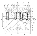
- FIG. 1 is a partial cross-sectional view of a semiconductor device 1.
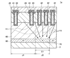
- FIG. It is a partial cross section figure of the semiconductor device 1a.
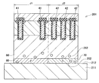
- 6 is a diagram illustrating a manufacturing process of the semiconductor device 1.
- FIG. 1 is a partial cross-sectional view of a semiconductor device 1.
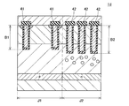
- FIG. 1 is a partial cross-sectional view of a semiconductor device 1.
- FIG. 1 is a partial cross-section figure of semiconductor device 1d.
- the electrode containing heavy metal is in contact with a part of the anode layer in the diode element region.
- the electrode containing heavy metal is in contact with a part of the cathode region in the diode element region.
- the depth of the second trench electrode is made deeper than the depth of the first trench electrode.
- the IGBT element region includes a planar type electrode.
- the wafer holding table is a transfer stage.
- As the heavy metal gold, platinum, silver, copper, chromium, cadmium, mercury, zinc, arsenic, manganese, cobalt, nickel, molybdenum, tungsten, or the like is used.
- FIG. 1 is a plan view of the semiconductor device 1 according to the first embodiment.
- the semiconductor device 1 is a reverse conducting semiconductor device in which IGBTs and diodes are mixed on the same semiconductor substrate.
- the display of the insulating film and the electrode on the trench is omitted for easy viewing.
- the semiconductor device 1 is manufactured using a semiconductor substrate 102 having an outer periphery 104.
- the semiconductor substrate 102 is divided into a cell area in which the IGBT element region J1 and the diode element region J2 are formed, and a termination area 107 surrounding the cell area.
- the cell area is a region in which electrodes for driving the IGBT element region J1 and the diode element region J2 are formed on the surface of the semiconductor substrate 102. Examples of such electrodes include the first electrode 5 and the second electrode 6 (see FIG. 2).
- the termination area 107 is an area where electrodes for driving the IGBT element area J1 and the diode element area J2 are not formed.
- electrodes (not shown) are formed in a region surrounded by a dotted line (IGBT element region J1 and diode element region J2).
- no electrode is formed outside the area surrounded by the dotted line (termination area 107).
- a floating electrode is formed on the surface of the semiconductor substrate 102. These regions do not correspond to the cell area because they are not electrodes for driving the IGBT element region J1 and the diode element region J2.
- a trench is formed at the boundary between the cell area and the termination area 107, or a region where the impurity concentration is higher than other regions is formed. Not applicable to area.
- first trenches 41 are formed so as to extend in the vertical direction of FIG.
- second trenches 42 are formed in the diode element region J2 so as to extend in the vertical direction of FIG.
- the openings of the first trench 41 and the second trench 42 have a rectangular closed loop shape.
- the total length of the opening boundary line that forms the opening of the first trench 41 per unit area of the IGBT element region J1 is defined as a length L1.
- the total length of the opening boundary line that forms the opening of the second trench 42 per unit area of the diode element region J2 is defined as a length L2.
- the area of the IGBT element region J1 and the area of the diode element region J2 are substantially the same.
- two first trenches 41 exist in the IGBT element region J1
- three second trenches 42 exist in the diode element region J2.
- the area of the opening of the first trench 41 and the area of the opening of the second trench 42 are substantially the same. Therefore, the length L2 is longer than the length L1.
- the diode element region J2 is in a state where trenches are formed at a higher density than the IGBT element region J1.
- the number of IGBT element regions J1 and diode element regions J2 included in the cell area is not limited to the description example of the present embodiment, and can be set to an arbitrary number. Further, the number of the first trenches 41 included in the IGBT element region J1 and the number of the second trenches 42 included in the diode element region J2 are not limited to the description example of the present embodiment, and may be set to an arbitrary number. Is possible.
- FIG. 2 is a partial cross-sectional view taken along line II-II in FIG.
- the semiconductor device 1 includes a semiconductor layer 2 made of silicon, a back electrode 3 formed on the back surface 2 b of the semiconductor layer 2, a first electrode 5, and a second electrode 6.
- the first electrode 5 is formed on the surface 2 a of the semiconductor layer 2.
- a trench 7 is formed in the first electrode 5.
- the second electrode 6 is formed on the surface of the first electrode 5 and inside the trench 7. Therefore, the second electrode 6 is in contact with a part of the shallow portion 2U in the diode element region J2 via the contact surface 7a.
- the first electrode 5 is an electrode that does not contain heavy metal.
- the second electrode 6 is an electrode containing heavy metal.
- the heavy metal is a metal element having a specific gravity of 4 to 5 or more, for example, Ni.
- An example of the material of the first electrode 5 is Al.
- the back electrode 3 continuously extends from the back surface of the IGBT element region J1 and the back surface of the diode element region J2.
- the semiconductor layer 2 includes a shallow portion 2U and a deep portion 2L.
- the deep portion 2L includes a p-type collector region 80 and an n-type cathode region 70.
- the collector region 80 is formed in the range of the IGBT element region J1 in the back surface 2b of the semiconductor layer 2.
- the cathode region 70 is formed in the diode element region J2 in the back surface 2b.
- the back electrode 3 described above is connected to the collector region 80 and the cathode region 70 in common.
- the deep portion 2L includes an n ⁇ type drift layer 60, and the drift layer 60 is formed in common on the collector region 80 and the cathode region 70.
- the drift layer 60 includes a heavy metal 62.
- the heavy metal 62 is represented by a white circle symbol in FIG.
- the density of heavy metals contained in the drift layer 60 in the diode element region J2 is set higher than the density of heavy metals contained in the drift layer 60 in the IGBT element region J1.
- the low lifetime region 61 is formed in at least a part of the drift layer 60 in the diode element region J2. Further, the low lifetime region 61 extends between the adjacent second trenches 42.
- the low lifetime region 61 is a region that contains heavy metal 62 at a higher concentration than the other regions of the drift layer 60.
- the heavy metal 62 has the effect of shortening the lifetime of the carrier.
- the lifetime of the hole in the low lifetime region 61 is shorter than the lifetime of the hole in the drift layer 60 in the IGBT element region J1 at the same depth as the low lifetime region 61.
- the heavy metal 62 does not necessarily have to be evenly distributed in the drift layer 60, and exhibits the effect as the low lifetime region 61 even when it is unevenly distributed.
- the IGBT element region J1 may contain heavy metal.
- the density of the heavy metal contained in the drift layer 60 in the diode element region J2 is set higher than the density of the heavy metal contained in the drift layer 60 in the IGBT element region J1, the IGBT element It is possible to ignore heavy metals in region J1. Therefore, in the subsequent drawings, the heavy metal notation (white circle symbol) in the IGBT element region J1 is omitted.
- a plurality of first trenches 41 and second trenches 42 are formed in the semiconductor layer 2.
- Each of the first trench 41 and the second trench 42 extends with its longitudinal direction aligned in the depth direction shown in FIG.
- Each trench extends from the surface 2 a of the semiconductor layer 2 in the depth direction of the semiconductor layer 2.
- the first trench electrode 11 is accommodated in the first trench 41 while being surrounded by the insulating film 14.
- the second trench electrode 12 is accommodated in the second trench 42 while being surrounded by the insulating film 14.
- the shallow portion 2U in the IGBT element region J1 is partitioned into a plurality of p-type body layers 30 by the first trench 41.
- the shallow portion 2U in the diode element region J2 is partitioned into a plurality of p-type anode layers 31 by the second trench 42.
- the body layer 30 in the IGBT element region J1 is provided with an n + -type emitter region 20.
- the emitter region 20 is exposed at a part of the surface 2 a of the semiconductor layer 2 and is in contact with the first trench 41. Therefore, the emitter region 20 is opposed to the second trench electrode 12 with the insulating film 14 interposed therebetween.
- the emitter region 20 is separated from the drift layer 60 by the body layer 30.
- the anode layer 31 in the diode element region J2 is exposed at a part of the surface 2a of the semiconductor layer 2 and is in contact with the second trench.
- the first electrode 5 formed on the surface 2a of the semiconductor layer 2 continuously extends on the surface of the IGBT element region J1 and the surface of the diode element region J2.
- the first electrode 5 is electrically connected to the emitter region 20 and the body layer 30.
- the first electrode 5 is electrically connected to the anode layer 31.
- An insulating film 10 is formed between the first trench electrode 11 and the second trench electrode 12 and the first electrode 5, and they are not electrically connected.
- the first trench electrode 11 and the second trench electrode 12 are connected to a gate wiring (not shown) in a region where the first electrode 5 is not formed (any cross section in the depth direction in FIG. 1).
- the semiconductor device 1 functioning as a reverse conducting IGBT is configured.
- the semiconductor device 1 functions as a circuit in which a diode composed of a diode element region J2 is connected in reverse parallel between a pair of main electrodes (between collector and emitter) of an IGBT composed of an IGBT element region J1.
- the semiconductor device 1 is used for driving an electric load represented by a motor.
- the length L2 (the total length of the opening boundary line of the second trench 42 per unit area of the diode element region J2) is the length L1 (per unit area of the IGBT element region J1). , The total length of the opening boundary line of the first trench 41).
- produces from the boundary surface of a trench and a semiconductor region, the one where the total length of an opening part boundary line is long generate
- the introduction of heavy metal 62 will be described.
- the second electrode 6 is in contact with a part of the shallow portion 2U in the diode element region J2 at the contact surface 7a.
- heavy metal 62 can be introduced into drift layer 60 in diode element region J2 through contact surface 7a.
- the crystal defect has a property of gettering (capturing and fixing) the heavy metal 62. Since the number of crystal defects in the drift layer 60 in the diode element region J2 is larger than the number of crystal defects in the drift layer 60 in the IGBT element region J1, the diode element region J2 includes the IGBT element region J1.
- the heavy metal 62 can be gettered at a higher density.
- the position of the contact surface 7a between the second electrode 6 and the shallow portion 2U will be described.
- the end position on the IGBT element region J1 side on the contact surface 7a in FIG. 2 is defined as a position P1.
- the end position of the emitter region 20 in the IGBT element region J1 on the diode element region J2 side is defined as a position P2.
- a distance between the position P1 and the position P2 is defined as a separation distance A1.
- the heavy metal 62 diffuses substantially concentrically in the shallow part 2U and the deep part 2L, starting from the contact surface 7a.
- the diffusion distance of heavy metal 62 at this time is defined as diffusion distance A2.
- the diffusion distance A2 is obtained by the following expression (1) (Arrhenius relational expression).
- A2 (D ⁇ t) 1/2 Formula (1)
- t is a diffusion time
- D is a diffusion coefficient.
- the diffusion coefficient D is obtained by the following equation (2).
- D D0 ⁇ exp ( ⁇ Ea / k ⁇ T) (2)
- Ea (eV) is the activation energy
- k (eV / K) is the Boltzmann constant
- T (K) is the absolute temperature. From the equations (1) and (2), it can be seen that the diffusion distance A2 of heavy metal is determined by the thermal history after forming the second electrode 6 and the physical constant.
- the separation distance A1 is equal to or greater than the diffusion distance A2.
- the separation distance A1 may be about 40 ⁇ m or more.
- FIG. 3 shows a partial cross-sectional view of the reverse conducting semiconductor device 1a.
- a region where a semiconductor region (cathode region 70) of the same conductivity type as the drift layer 60 (n-type) is in contact with the back electrode 3 is defined as a collector short region C1.
- carriers are injected toward the collector short region C1 not only from the diode element region J2 side but also from the IGBT element region J1 side. That is, the IGBT element region J1 also operates as a diode. Therefore, it is difficult to clearly specify the boundary between the IGBT element region J1 and the diode element region J2.
- the region where the collector short region (cathode region 70) exists and the emitter region 20 does not exist is This is defined as a diode element region J2.
- the emitter region 20 does not exist over the entire region of the collector short region C1. Therefore, in the semiconductor device 1a, the region including all of the collector short region C1 is the diode element region J2.
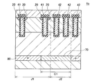
- FIG. 4 shows a partial cross-sectional view of the semiconductor device 1b.
- the emitter region 20 does not exist above a part of the collector short region C1. Therefore, in the semiconductor device 1b, a part of the collector short region C1 becomes the diode element region J2.
- the technique of the present application can also be applied to a semiconductor device including the diode element region J2 having a narrower width than the collector short region C1.
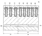
- FIG. 5 shows a partial cross-sectional view of the semiconductor device 1c.
- a dummy trench 43 is formed in the IGBT element region J1.
- the dummy trench 43 is a trench in which the emitter region 20 is not formed.
- the collector region 80 is present vertically below the dummy trench 43 (lower side in FIG. 5), and the collector short region C1 is not present. Therefore, the dummy trench 43 is not regarded as the diode element region J2.
- the form of the dummy trench is not limited to the form of FIG.
- the dummy trench includes a trench in which a floating potential or an emitter potential is applied to the trench electrode instead of the gate potential.
- the operation of the semiconductor device 1 will be described.
- a case where the IGBT element region J1 is turned on will be described.
- a higher voltage than the first electrode 5 is applied to the back electrode 3 of the semiconductor device 1.
- a gate voltage (gate on voltage) equal to or higher than a threshold is applied to the first trench electrode 11 and the second trench electrode 12.
- the body layer 30 facing the second trench electrode 12 via the insulating film 14 is inverted to n-type, and an n-type channel is formed.
- electrons flowing out from the emitter region 20 are injected into the drift layer 60 through the n-type channel.
- the diode element region J2 is in a conductive state.
- a forward voltage higher than that of the back electrode 3 is applied to the first electrode 5 of the semiconductor device 1.
- the gate-on voltage is not applied to the first trench electrode 11 and the second trench electrode 12.
- holes flow out from the body layer 30 and anode layer 31 side to the drift layer 60 side in both the diode element region J2 and the IGBT element region J1.
- electrons move from the cathode region 70 toward the drift layer 60.
- the diode element region J2 becomes conductive.
- the diode element region J2 is changed from the conductive state to the nonconductive state.
- a forward voltage higher than that of the back electrode 3 is applied to the first electrode 5
- a hole is formed from the anode layer 31 side to the drift layer 60 side. Will not leak.
- the diode element region J2 is turned off.
- the holes injected into the drift layer 60 try to return to the anode layer 31.
- the semiconductor device 1 of FIG. 2 includes a low lifetime region 61 in the drift layer 60 in the diode element region J2. Thereby, part of the holes returning to the anode layer 31 disappears in the low lifetime region 61 during the recovery operation of the diode element region J2. Therefore, the recovery current in the diode element region J2 can be reduced, and the recovery loss in the diode element region J2 can be reduced.
- the low lifetime region 61 is not formed in the IGBT element region J1.
- the IGBT element region J1 holes existing in the drift layer 60 are difficult to disappear when the IGBT element region J1 is in the on state, and conductivity modulation is actively performed.
- the on-voltage of the IGBT element region J1 is low as in the case where the low lifetime region 61 is not formed. Therefore, according to the semiconductor device 1 of FIG. 2, the recovery loss can be reduced without increasing the on-voltage of the IGBT element region J1.
- Crystal defects can be introduced in Control of the shape and the like when forming the trench can be performed with higher accuracy than control of the range and distribution of irradiated ions. Therefore, distribution control of crystal defects can be performed with higher accuracy. Further, in the semiconductor device according to the first embodiment, the step of forming the trench electrode and the step of introducing defects can be shared. Accordingly, it is possible to eliminate the necessity of separately providing a process for introducing a defect, such as a process for forming an irradiation mask, and thus manufacturing costs can be reduced.
- the lifetime killer (heavy metal) is distributed by thermal diffusion. Then, the distribution control of the lifetime killer can be performed by the heat history and the physical constant. Therefore, since there are few parameters to handle, it is possible to perform lifetime killer distribution control with higher accuracy.
- heavy metal is used as a lifetime killer. Heavy metals are more effective as lifetime killer than crystal defects. Therefore, the recovery loss in the diode element region J2 can be more effectively reduced. Further, heavy metals have a larger diffusion coefficient than impurities normally used in semiconductors (eg, boron (B), etc.). For example, boron (B) used in the diffusion layer moves on the micrometer order by the heating process. On the other hand, heavy metals move on the order of millimeters by the heating process. If crystal defects are formed at a higher density in the diode element region J2 than in the IGBT element region J1 by controlling the trench density, the heavy metal is gettered at a higher density by the diode element region J2.
- impurities normally used in semiconductors eg, boron (B), etc.
- boron (B) used in the diffusion layer moves on the micrometer order by the heating process.
- heavy metals move on the order of millimeters by the heating process.
- the heavy metal moves to the diode element region J2 due to heat during the manufacturing process, and the heavy metal is gettered to crystal defects in the diode element region J2. That is, the heavy metal is moved by the heating process so that the density of the heavy metal contained in the drift layer 60 in the diode element region J2 is higher than the density of the heavy metal contained in the drift layer 60 in the IGBT element region J1. Can do. Therefore, since the low lifetime region is given to the diode element region J2 with high accuracy, the diode element region J2 can be reduced in recovery.
- the second electrode 6 containing heavy metal has a structure in which a part of the diode element region J2 is in contact with the contact surface 7a.
- the 2nd electrode 6 can be used also as a member for introducing a heavy metal. Therefore, it is possible to eliminate the necessity of separately providing a dedicated member for introducing the heavy metal, so that the manufacturing cost can be suppressed.
- the diode element region J2 there is a configuration in which crystal defects are concentrated in the vicinity of the tip of the trench.
- the tip of the trench is one of the parts where the electric field is highest. Therefore, if crystal defects are concentrated in the vicinity of the tip of the trench, there is a risk that leakage current increases or carriers are accelerated by a high electric field and avalanche breakdown is likely to occur.
- the trench interval in the diode element region J2 is narrower than the trench interval in the IGBT element region J1.
- crystal defects can be formed over a wide range not only near the tip of the second trench 42 but also around the second trench 42 due to thermal stress generated in the entire second trench 42. As a result, it is possible to prevent the occurrence of leakage current and avalanche breakdown.
- the trench interval in the diode element region J2 is narrower than the trench interval in the IGBT element region J1. Therefore, in the diode element region J2, the depletion layer is more easily connected between adjacent trenches, so that the electric field at the tip of the trench can be made difficult to increase.
- the breakdown voltage of the IGBT element region J1 and the breakdown voltage of the diode element region J2 can be individually adjusted without using the substrate resistance or the like. That is, the breakdown voltage of the diode element region J2 can be made higher than the breakdown voltage of the IGBT element region J1. Therefore, it is possible to reduce the area of the diode element region J2 while ensuring the avalanche resistance (breakdown resistance) (thermal mass), and thus the chip size can be reduced.
- step S11 of FIG. 6 trenches are formed from the wafer surface side in the IGBT element region J1 and the diode element region J2.
- the formation density of the second trenches 42 formed in the diode element region J2 is set higher than the formation density of the first trenches 41 formed in the IGBT element region J1.
- the trench is formed in a state where a heavy metal gettering layer is present on the back surface of the wafer.
- a gettering layer is a layer for trapping impurities such as heavy metals. The gettering layer can prevent heavy metal contamination of the device active region.
- a conventionally well-known process can be used for the process of forming the element structure on the wafer surface, the description is omitted here.
- step S12 a surface protective tape is applied to the wafer surface. Thereby, since the wafer front surface side can be brought into contact with the stage or the like, the wafer can be placed on the stage so that the wafer back surface side is exposed.
- step S13 the back surface of the wafer is polished. Thereby, the heavy metal gettering layer formed on the back surface of the wafer is removed.
- step S14 wet etching is performed to clean the polished surface of the wafer.
- the cathode region 70 and the collector region 80 are formed by performing ion implantation from the back surface of the wafer.
- step S15 a surface protection tape peeling process is performed.
- the wafer 201 is placed on the stage 211 so that the back surface 202 of the wafer 201 is in contact with the front surface 212 of the stage 211 as shown in FIG. Further, in the stage 211, a portion in contact with the back surface 202 of the wafer 201 is formed of a material containing heavy metal.
- the heavy metal 262 of the stage 211 is introduced into the wafer 201 through the contact portion between the back surface 202 of the wafer 201 and the front surface 212 of the stage 211.
- the heavy metal 262 is represented by a white circle symbol in FIG.
- step S16 a heating process is performed.
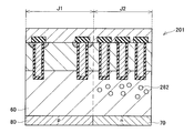
- the heavy metal 262 in the wafer 201 is diffused by the heating process.
- crystal defects are formed at a higher density in the diode element region J2 by controlling the trench density in step S11 described above. Therefore, as shown in FIG. 8, the heavy metal 262 is gettered at a higher density on the diode element region J2 side. That is, the heavy metal 262 is moved by the heating process so that the density of the heavy metal contained in the drift layer 60 in the diode element region J2 is higher than the density of the heavy metal contained in the drift layer 60 in the IGBT element region J1. be able to. Further, the regions (cathode region 70 and collector region 80) where ion implantation has been performed on the back surface of the wafer can be activated by the heating process.
- a heating step (step S16) is provided after the step (step S15) of bringing the wafer into contact with a stage using a heavy metal material.
- the heavy metal introduced from the stage can be diffused and gettered to a minute defect. Therefore, the heavy metal is moved by the heating step so that the density of the heavy metal contained in the drift layer 60 in the diode element region J2 is higher than the density of the heavy metal contained in the drift layer 60 in the IGBT element region J1. Can do.
- the heavy metal is removed from the wafer while the gettering layer is removed by the step of polishing the back surface of the wafer (step S13). Can be introduced in. Therefore, heavy metal can be sufficiently diffused in the semiconductor layer.
- FIG. 9 shows a partial cross-sectional view of the semiconductor device 1d.
- the depth B2 of the second trench 42 in the diode element region J2 is deeper than the depth B1 of the first trench 41 in the IGBT element region J1.
- the thermal stress can be generated in a wider region in the diode element region J2 than in the IGBT element region J1 in the depth direction. Therefore, crystal defects can be formed at a higher density in the diode element region J2.
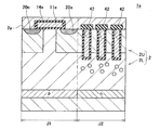
- FIG. 10 is a partial cross-sectional view of the semiconductor device 1e.
- the semiconductor device 1e is different from the semiconductor device 1 (FIG. 2) in that the IGBT element region J1 includes a planar first electrode 11e.
- the first electrode 11e is formed on the surface 2a of the semiconductor layer 2 in a state surrounded by the insulating film 14e. A part of the emitter region 20e is exposed to the surface 2a of the semiconductor layer 2, and a part thereof is in contact with the first electrode 11e.
- a trench is not formed in the IGBT element region J1, but a trench is formed only in the diode element region J2. Therefore, since crystal defects due to the trench can be formed only in the diode element region J2, crystal defects can be generated at a higher density in the diode element region J2 than in the IGBT element region J1.
- the present invention is not limited to this configuration.
- the trench can be arranged in various configurations. In FIGS. 11 to 14, the trench portion is indicated by hatching.
- the diode element region J2 has trenches formed at a higher density than the IGBT element region J1.
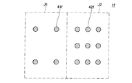
- a semiconductor device 1f shown in FIG. 11 is an example in which trenches are arranged in a dot shape.
- the openings of the first trench 41f and the second trench 42f are circular. Then, four first trenches 41f are formed in the IGBT element region J1, and nine second trenches 42f are formed in the diode element region J2.
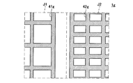
- a semiconductor device 1g shown in FIG. 12 is an example in which trenches are arranged in a lattice shape.
- the diode element region J2 has a higher lattice density than the IGBT element region J1. Therefore, the total length of the opening boundary line of the second trench 42g is longer than the total length of the opening boundary line of the first trench 41g.
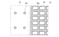
- a semiconductor device 1h shown in FIG. 13 is an example in which a dot-shaped first trench 41f (FIG. 11) and a lattice-shaped second trench 42g (FIG. 12) are combined.
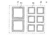
- the semiconductor device 1i shown in FIG. 14 is an example in which trenches are arranged in a discontinuous lattice shape.
- the diode element region J2 has a higher lattice density than the IGBT element region J1. Therefore, the total length of the opening boundary line of the second trench 42 i is longer than the total length of the opening boundary line of the first trench 41 i.
- the method for determining the separation distance A1 is not limited to the method based on the diffusion distance A2.
- the separation distance A1 may be determined to be not less than the distance A3 (FIG. 2) determined by the sum of the thickness of the anode layer 31 and the thickness of the drift layer 60 in the diode element region J2.
- the arrangement form of the second electrode containing heavy metal is not limited to the example of FIG.
- the second electrode 6j is formed on the surface of the back electrode 3 and inside the trench 8. Therefore, the second electrode 6j is in contact with a part of the cathode region 70 in the diode element region J2 via the contact surface 8a.
- the second electrode 6 k is formed inside the cavity 9 of the first electrode 5. Therefore, the second electrode 6k is not exposed on the surface of the semiconductor device 1k.
- the second electrode 6k is in contact with a part of the shallow portion 2U in the diode element region J2 via the contact surface 9a.
- the second electrode 6m is formed on the surface of the first electrode 5 in the diode element region J2 and in the trench 51.
- the second electrode 6m is in contact with a part of the shallow portion 2U in the diode element region J2 via the contact surface 51a.
- the second electrode 6n is formed on the surface of the back electrode 3 in the diode element region J2 and in the trench 52.
- the second electrode 6n is in contact with a part of the cathode region 70 in the diode element region J2 via the contact surface 52a.
- the density of the heavy metal contained in the drift layer 60 in the diode element region J2 is higher than the density of the heavy metal contained in the drift layer 60 in the IGBT element region J1. is there. Therefore, it is not always necessary to introduce crystal defects into the drift layer 60 in the diode element region J2. Therefore, as shown in FIGS. 16 to 18, it is possible to adopt a mode in which no trench is formed in the diode element region J2.
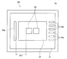
- FIG. 19 is a top view of the separated reverse conducting semiconductor device 1p.
- the separated type semiconductor device is a semiconductor device in which the IGBT element region J1 and the diode element region J2 are formed together in one region.
- two contact surfaces 53 that are in contact with the second electrode containing heavy metal are formed in the diode element region J2.
- a plurality of emitter regions 20p are formed in the IGBT element region J1.
- the separation distance A11 is preferably set to be the diffusion distance A2 or the distance A3 or more.
- the contact surface 53 and the emitter region 20p may have various shapes, for example, a dot shape or a stripe shape, or various shapes may be mixed.
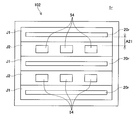
- FIG. 20 shows a top view of the mixed type reverse conducting semiconductor device 1r.
- the mixed type semiconductor device is a semiconductor device in which the IGBT element region J1 and the diode element region J2 are each divided into a plurality of regions.
- the semiconductor device 1r three IGBT element regions J1 and two diode element regions J2 are alternately arranged.
- three contact surfaces 54 that are in contact with the second electrode containing heavy metal are formed.
- An emitter region 20r is formed in the IGBT element region J1.
- the separation distance A21 is preferably set to be equal to or more than the diffusion distance A2 and the distance A3 described above.
- the electrode used for other uses is required between the solder and the element.
- an electrode made of Ni (corresponding to the second electrode 6 in FIG. 2) is formed on the surface of the electrode made of Al (corresponding to the first electrode 5 in FIG. 2). This eliminates the need to separately form a dedicated electrode for introducing heavy metal, thereby reducing manufacturing costs.
- the electrode formed of Ni can be formed by various methods such as plating or sputtering.
- the second electrode containing heavy metal may be in contact with the semiconductor layer in the diode element region J2 through the intermediate layer.
- the intermediate layer is a layer having a property of diffusing heavy metals.
- the thickness of the intermediate layer is made smaller than the diffusion distance A2 of heavy metal contained in the electrode.
- Examples of the intermediate layer include a silicon oxide film.
- the heavy metal contained in the second electrode may be a metal having a specific gravity of 4 or more.
- examples include iron, lead, gold, platinum, silver, copper, chromium, cadmium, mercury, zinc, arsenic, manganese, cobalt, nickel, molybdenum, tungsten, tin, bismuth, uranium, and plutonium.
- ⁇ Modification of Example 2> A modification of the semiconductor device according to the second embodiment will be described below.
- the transfer stage is a full-surface holding stage having a holding surface that comes into contact with the entire back surface of the wafer.
- the holding surface is made of a material containing heavy metal.
- the timing for using the transport stage for introducing heavy metal may be any timing as long as the heavy metal gettering by the thermal process is completed after the heavy metal gettering layer on the back surface of the wafer is removed.
Landscapes
- Metal-Oxide And Bipolar Metal-Oxide Semiconductor Integrated Circuits (AREA)
Abstract
Description
(特徴1)重金属を含む電極は、ダイオード素子領域内のアノード層の一部と接触している。
(特徴2)重金属を含む電極は、ダイオード素子領域内のカソード領域の一部と接触している。
(特徴3)第1トレンチ電極の深さに比して、第2トレンチ電極の深さが深くされている。
(特徴4)IGBT素子領域は、プレーナ型の電極を備えている。
(特徴5)ウェハ保持台は、搬送ステージである。
(特徴6)重金属は、金、白金、銀、銅、クロム、カドミウム、水銀、亜鉛、ヒ素、マンガン、コバルト、ニッケル、モリブデン、タングステン等が用いられる。
A2=(D×t)1/2・・・式(1)
ここで、tは拡散時間、Dは拡散係数である。また、拡散係数Dは、下式(2)で求められる。
D=D0×exp(-Ea/k×T)・・・式(2)
ここで、D0(cm2/s)は拡散定数、Ea(eV)は活性化エネルギー、k(eV/K)はボルツマン定数、T(K)は絶対温度、である。式(1)および式(2)により、重金属の拡散距離A2は、第2電極6を形成した後の熱履歴と、物理定数により決定されることが分かる。
実施例1に係る半導体装置の変形例を、以下に説明する。図9に、半導体装置1dの一部断面図を示す。半導体装置1dは、IGBT素子領域J1内の第1トレンチ41の深さB1に比して、ダイオード素子領域J2内の第2トレンチ42の深さB2が深くされている点が、半導体装置1(図2)と異なっている。これにより、IGBT素子領域J1よりもダイオード素子領域J2の方が、深さ方向についても、より広い領域に熱応力を発生させることができる。よって、ダイオード素子領域J2に、より高密度で結晶欠陥を形成することができる。
実施例2に係る半導体装置の変形例を、以下に説明する。図6のステップS13において裏面研磨が行われた後において、重金属導入用の搬送ステージを使用する形態であってもよい。当該搬送ステージは、ウェハの裏面の全面と接触する保持面を備える、全面保持ステージである。また保持面は、重金属を含む材料で形成されている。これにより、ウェハの搬送時において、保持面とウェハ裏面とを接触させることで、ウェハ内に重金属を導入することができる。また、ウェハの全面を保持することでウェハに反りやたわみを発生させにくくすることができるため、大口径ウェハや薄化されたウェハを確実に搬送することが可能となる。なお、重金属導入用の搬送ステージを使用するタイミングは、ウェハ裏面の重金属ゲッタリング層が除去されてから、熱工程による重金属ゲッタリングが完了するまでの間であれば、何れのタイミングでもよい。
Claims (10)
- 同一半導体基板にIGBT素子領域とダイオード素子領域が混在している半導体装置であり、
IGBT素子領域は、第2導電型のドリフト層と第1導電型のボディ層を備えており、
ダイオード素子領域は、第2導電型のドリフト層と第1導電型のアノード層を備えており、
ダイオード素子領域のドリフト層に含まれる重金属の密度が、IGBT素子領域のドリフト層に含まれる重金属の密度に比して高いことを特徴とする半導体装置。 - IGBT素子領域では、第1導電型のコレクタ層と第2導電型のドリフト層と第1導電型のボディ層が順に積層されており、
ボディ層の表面からボディ層を貫通してドリフト層内に突出しているとともに絶縁膜で囲まれている第1トレンチ電極が形成されており、
その絶縁膜を介して第1トレンチ電極に接しているとともに半導体基板の表面に臨む範囲に第2導電型のエミッタ領域が形成されており、そのエミッタ領域がボディ層によってドリフト層から分離されており、
ダイオード素子領域では、第2導電型のカソード層と第2導電型のドリフト層と第1導電型のアノード層が順に積層されており、
アノード層の表面からアノード層を貫通してドリフト層内に突出しているとともに絶縁膜で囲まれている第2トレンチ電極が形成されており、
第1トレンチ電極の開口部が形成されているボディ層の表面、および、第2トレンチ電極の開口部が形成されているアノード層の表面を観測したときに、ダイオード素子領域の単位面積あたりの第2トレンチ電極の開口部を形成する開口部境界線の合計長さが、IGBT素子領域の単位面積あたりの第1トレンチ電極の開口部を形成する開口部境界線の合計長さに比して長くされていることを特徴とする請求項1に記載の半導体装置。 - 重金属を含む電極をさらに備え、
ダイオード領域内の半導体層の少なくとも一部と電極とが接触していることを特徴とする請求項1または2に記載の半導体装置。 - 重金属を含む電極とダイオード素子領域内の半導体層とが接触する接触領域と、IGBT素子領域内のエミッタ領域との間の第1距離が、電極に含まれる重金属の拡散距離以上であることを特徴とする請求項3に記載の半導体装置。
- 第1距離が、ダイオード素子領域のカソード層の厚さとドリフト層の厚さの和によって定まる第2距離以上であることを特徴とする請求項4に記載の半導体装置。
- ダイオード領域内の半導体層と重金属を含む電極とが、重金属を拡散する性質を有する中間層を介して接触しており、
中間層の厚さは、電極に含まれている重金属の拡散距離よりも小さくされていることを特徴とする請求項3ないし5の何れか1項に記載の半導体装置。 - 同一半導体基板にIGBT素子領域とダイオード素子領域が混在している半導体装置であり、
IGBT素子領域では、第1導電型のコレクタ層と第2導電型のドリフト層と第1導電型のボディ層が順に積層されており、
ボディ層の表面からボディ層を貫通してドリフト層内に突出しているとともに絶縁膜で囲まれている第1トレンチ電極が形成されており、
その絶縁膜を介して第1トレンチ電極に接しているとともに半導体基板の表面に臨む範囲に第2導電型のエミッタ領域が形成されており、そのエミッタ領域がボディ層によってドリフト層から分離されており、
ダイオード素子領域では、第2導電型のカソード層と第2導電型のドリフト層と第1導電型のアノード層が順に積層されており、
アノード層の表面からアノード層を貫通してドリフト層内に突出しているとともに絶縁膜で囲まれている第2トレンチ電極が形成されており、
第1トレンチ電極の開口部が形成されているボディ層の表面、および、第2トレンチ電極の開口部が形成されているアノード層の表面を観測したときに、ダイオード素子領域の単位面積あたりの第2トレンチ電極の開口部を形成する開口部境界線の合計長さが、IGBT素子領域の単位面積あたりの第1トレンチ電極の開口部を形成する開口部境界線の合計長さに比して長くされていることを特徴とする半導体装置。 - 同一半導体基板にIGBT素子領域とダイオード素子領域が混在している半導体装置の製造方法であって、
重金属を含むウェハ保持台にウェハを接触させる接触工程と、
接触工程の後に、ウェハを加熱する加熱工程と、
を備えることを特徴とする半導体装置の製造方法。 - IGBT素子領域に第1トレンチ電極を形成する第1形成工程と、
ダイオード素子領域に第2トレンチ電極を形成する第2形成工程と、
をさらに備え、
第1形成工程と第2形成工程が行われたウェハを表面から観測したときに、ダイオード素子領域の単位面積あたりの第2トレンチ電極の開口部を形成する開口部境界線の合計長さが、IGBT素子領域の単位面積あたりの第1トレンチ電極の開口部を形成する開口部境界線の合計長さに比して長くされており、
第1形成工程および第2形成工程は、加熱工程の前に行われることを特徴とする請求項8に記載の製造方法。 - ウェハの裏面を研磨する研磨工程をさらに備え、
研磨工程は、接触工程の前に行われることを特徴とする請求項8または9に記載の製造方法。
Priority Applications (5)
| Application Number | Priority Date | Filing Date | Title |
|---|---|---|---|
| JP2013519318A JP5630579B2 (ja) | 2011-06-09 | 2011-06-09 | 半導体装置および半導体装置の製造方法 |
| US14/002,522 US9064711B2 (en) | 2011-06-09 | 2011-06-09 | Semiconductor device and method for fabricating semiconductor device |
| DE112011105319.3T DE112011105319B4 (de) | 2011-06-09 | 2011-06-09 | Halbleitervorrichtung und Verfahren zur Herstellung einer Halbleitervorrichtung |
| CN201180071452.3A CN103582936B (zh) | 2011-06-09 | 2011-06-09 | 半导体装置以及半导体装置的制造方法 |
| PCT/JP2011/063280 WO2012169053A1 (ja) | 2011-06-09 | 2011-06-09 | 半導体装置および半導体装置の製造方法 |
Applications Claiming Priority (1)
| Application Number | Priority Date | Filing Date | Title |
|---|---|---|---|
| PCT/JP2011/063280 WO2012169053A1 (ja) | 2011-06-09 | 2011-06-09 | 半導体装置および半導体装置の製造方法 |
Publications (1)
| Publication Number | Publication Date |
|---|---|
| WO2012169053A1 true WO2012169053A1 (ja) | 2012-12-13 |
Family
ID=47295655
Family Applications (1)
| Application Number | Title | Priority Date | Filing Date |
|---|---|---|---|
| PCT/JP2011/063280 Ceased WO2012169053A1 (ja) | 2011-06-09 | 2011-06-09 | 半導体装置および半導体装置の製造方法 |
Country Status (5)
| Country | Link |
|---|---|
| US (1) | US9064711B2 (ja) |
| JP (1) | JP5630579B2 (ja) |
| CN (1) | CN103582936B (ja) |
| DE (1) | DE112011105319B4 (ja) |
| WO (1) | WO2012169053A1 (ja) |
Cited By (8)
| Publication number | Priority date | Publication date | Assignee | Title |
|---|---|---|---|---|
| JP2014175517A (ja) * | 2013-03-11 | 2014-09-22 | Mitsubishi Electric Corp | 半導体装置およびその製造方法 |
| WO2015068203A1 (ja) * | 2013-11-05 | 2015-05-14 | トヨタ自動車株式会社 | 半導体装置 |
| WO2017138231A1 (ja) * | 2016-02-10 | 2017-08-17 | 株式会社デンソー | 半導体装置 |
| JP2017157851A (ja) * | 2013-03-29 | 2017-09-07 | 富士電機株式会社 | 半導体装置および半導体装置の製造方法 |
| JP2021190657A (ja) * | 2020-06-04 | 2021-12-13 | 三菱電機株式会社 | 半導体装置 |
| US11276771B2 (en) | 2018-05-17 | 2022-03-15 | Fuji Electric Co., Ltd. | Semiconductor device |
| WO2023188561A1 (ja) * | 2022-03-28 | 2023-10-05 | 株式会社日立パワーデバイス | 半導体装置および電力変換装置 |
| WO2024185360A1 (ja) * | 2023-03-06 | 2024-09-12 | ローム株式会社 | 逆導通igbtおよび逆導通igbtの製造方法 |
Families Citing this family (18)
| Publication number | Priority date | Publication date | Assignee | Title |
|---|---|---|---|---|
| JP6181597B2 (ja) * | 2014-04-28 | 2017-08-16 | トヨタ自動車株式会社 | 半導体装置及び半導体装置の製造方法 |
| DE112015000610T5 (de) * | 2014-09-04 | 2016-11-17 | Fuji Electric Co., Ltd. | Halbleitervorrichtung und Verfahren zum Herstellen einer Halbleitervorrichtung |
| CN105814694B (zh) * | 2014-10-03 | 2019-03-08 | 富士电机株式会社 | 半导体装置以及半导体装置的制造方法 |
| JP6261494B2 (ja) * | 2014-12-03 | 2018-01-17 | 三菱電機株式会社 | 電力用半導体装置 |
| US9755058B2 (en) * | 2015-02-27 | 2017-09-05 | D3 Semiconductor LLC | Surface devices within a vertical power device |
| JP6274154B2 (ja) | 2015-05-27 | 2018-02-07 | トヨタ自動車株式会社 | 逆導通igbt |
| US10056370B2 (en) * | 2015-07-16 | 2018-08-21 | Fuji Electric Co., Ltd. | Semiconductor device |
| JP6582762B2 (ja) * | 2015-09-03 | 2019-10-02 | 株式会社デンソー | 半導体装置 |
| JP6314965B2 (ja) * | 2015-12-11 | 2018-04-25 | トヨタ自動車株式会社 | 半導体装置の製造方法 |
| JP7001104B2 (ja) * | 2017-12-14 | 2022-01-19 | 富士電機株式会社 | 半導体装置 |
| JP7095303B2 (ja) * | 2018-02-14 | 2022-07-05 | 富士電機株式会社 | 半導体装置 |
| JP2019145708A (ja) | 2018-02-22 | 2019-08-29 | 株式会社東芝 | 半導体装置 |
| CN109713037B (zh) * | 2018-12-29 | 2021-11-23 | 安建科技(深圳)有限公司 | 一种绝缘栅双极性晶体管器件及其制备方法 |
| JP7189848B2 (ja) | 2019-08-07 | 2022-12-14 | 株式会社東芝 | 半導体装置およびその製造方法 |
| WO2021254615A1 (en) * | 2020-06-18 | 2021-12-23 | Dynex Semiconductor Limited | Reverse conducting igbt with controlled anode injection |
| JP7456902B2 (ja) * | 2020-09-17 | 2024-03-27 | 株式会社東芝 | 半導体装置 |
| CN114256066B (zh) * | 2020-09-22 | 2025-03-21 | 珠海格力电器股份有限公司 | 一种少子寿命控制方法 |
| CN119855178A (zh) * | 2025-03-21 | 2025-04-18 | 上海维安半导体有限公司 | 一种折中正向和反向特性的rc-igbt器件及其制备方法 |
Citations (5)
| Publication number | Priority date | Publication date | Assignee | Title |
|---|---|---|---|---|
| JPS6376456A (ja) * | 1986-09-19 | 1988-04-06 | Hitachi Ltd | 銅電極を用いた半導体装置 |
| JP2004363327A (ja) * | 2003-06-04 | 2004-12-24 | Fuji Electric Device Technology Co Ltd | 半導体装置 |
| JP2007317883A (ja) * | 2006-05-25 | 2007-12-06 | Toyota Motor Corp | 半導体装置の製造方法 |
| JP2009272550A (ja) * | 2008-05-09 | 2009-11-19 | Toyota Motor Corp | 半導体装置 |
| JP2010171385A (ja) * | 2008-12-24 | 2010-08-05 | Denso Corp | 半導体装置 |
Family Cites Families (13)
| Publication number | Priority date | Publication date | Assignee | Title |
|---|---|---|---|---|
| JPH0691233B2 (ja) | 1984-12-03 | 1994-11-14 | 新技術事業団 | 半導体受光素子の製造方法 |
| JPH04125933A (ja) | 1990-09-17 | 1992-04-27 | Toshiba Corp | 半導体装置の製造方法 |
| JP4165079B2 (ja) | 2002-01-30 | 2008-10-15 | 富士電機デバイステクノロジー株式会社 | 半導体装置 |
| DE102004012884B4 (de) | 2004-03-16 | 2011-07-21 | IXYS Semiconductor GmbH, 68623 | Leistungs-Halbleiterbauelement in Planartechnik |
| JP4791704B2 (ja) | 2004-04-28 | 2011-10-12 | 三菱電機株式会社 | 逆導通型半導体素子とその製造方法 |
| JP2008192737A (ja) | 2007-02-02 | 2008-08-21 | Denso Corp | 半導体装置 |
| EP2003694B1 (en) * | 2007-06-14 | 2011-11-23 | Denso Corporation | Semiconductor device |
| JP4605251B2 (ja) * | 2007-06-14 | 2011-01-05 | 株式会社デンソー | 半導体装置 |
| JP4840370B2 (ja) * | 2008-01-16 | 2011-12-21 | トヨタ自動車株式会社 | 半導体装置とその半導体装置を備えている給電装置の駆動方法 |
| JP2010263149A (ja) | 2009-05-11 | 2010-11-18 | Toyota Motor Corp | 半導体装置 |
| EP2477226B1 (en) * | 2009-09-07 | 2016-06-22 | Toyota Jidosha Kabushiki Kaisha | Semiconductor device including semiconductor substrate having diode region and igbt region |
| JP4957840B2 (ja) * | 2010-02-05 | 2012-06-20 | 株式会社デンソー | 絶縁ゲート型半導体装置 |
| JP5348276B2 (ja) * | 2011-07-04 | 2013-11-20 | 株式会社デンソー | 半導体装置 |
-
2011
- 2011-06-09 WO PCT/JP2011/063280 patent/WO2012169053A1/ja not_active Ceased
- 2011-06-09 JP JP2013519318A patent/JP5630579B2/ja not_active Expired - Fee Related
- 2011-06-09 DE DE112011105319.3T patent/DE112011105319B4/de not_active Expired - Fee Related
- 2011-06-09 CN CN201180071452.3A patent/CN103582936B/zh not_active Expired - Fee Related
- 2011-06-09 US US14/002,522 patent/US9064711B2/en active Active
Patent Citations (5)
| Publication number | Priority date | Publication date | Assignee | Title |
|---|---|---|---|---|
| JPS6376456A (ja) * | 1986-09-19 | 1988-04-06 | Hitachi Ltd | 銅電極を用いた半導体装置 |
| JP2004363327A (ja) * | 2003-06-04 | 2004-12-24 | Fuji Electric Device Technology Co Ltd | 半導体装置 |
| JP2007317883A (ja) * | 2006-05-25 | 2007-12-06 | Toyota Motor Corp | 半導体装置の製造方法 |
| JP2009272550A (ja) * | 2008-05-09 | 2009-11-19 | Toyota Motor Corp | 半導体装置 |
| JP2010171385A (ja) * | 2008-12-24 | 2010-08-05 | Denso Corp | 半導体装置 |
Cited By (16)
| Publication number | Priority date | Publication date | Assignee | Title |
|---|---|---|---|---|
| JP2014175517A (ja) * | 2013-03-11 | 2014-09-22 | Mitsubishi Electric Corp | 半導体装置およびその製造方法 |
| JP2017157851A (ja) * | 2013-03-29 | 2017-09-07 | 富士電機株式会社 | 半導体装置および半導体装置の製造方法 |
| CN105706238B (zh) * | 2013-11-05 | 2019-03-12 | 丰田自动车株式会社 | 半导体装置 |
| WO2015068203A1 (ja) * | 2013-11-05 | 2015-05-14 | トヨタ自動車株式会社 | 半導体装置 |
| CN105706238A (zh) * | 2013-11-05 | 2016-06-22 | 丰田自动车株式会社 | 半导体装置 |
| JPWO2015068203A1 (ja) * | 2013-11-05 | 2017-03-09 | トヨタ自動車株式会社 | 半導体装置 |
| DE112013007576B4 (de) | 2013-11-05 | 2022-02-03 | Denso Corporation | Halbleitereinrichtung |
| US9960165B2 (en) | 2013-11-05 | 2018-05-01 | Toyota Jidosha Kabushiki Kaisha | Semiconductor device having adjacent IGBT and diode regions with a shifted boundary plane between a collector region and a cathode region |
| WO2017138231A1 (ja) * | 2016-02-10 | 2017-08-17 | 株式会社デンソー | 半導体装置 |
| JP2017143195A (ja) * | 2016-02-10 | 2017-08-17 | 株式会社デンソー | 半導体装置 |
| US11276771B2 (en) | 2018-05-17 | 2022-03-15 | Fuji Electric Co., Ltd. | Semiconductor device |
| JP2021190657A (ja) * | 2020-06-04 | 2021-12-13 | 三菱電機株式会社 | 半導体装置 |
| JP7459666B2 (ja) | 2020-06-04 | 2024-04-02 | 三菱電機株式会社 | 半導体装置 |
| WO2023188561A1 (ja) * | 2022-03-28 | 2023-10-05 | 株式会社日立パワーデバイス | 半導体装置および電力変換装置 |
| JP2023144467A (ja) * | 2022-03-28 | 2023-10-11 | 株式会社 日立パワーデバイス | 半導体装置および電力変換装置 |
| WO2024185360A1 (ja) * | 2023-03-06 | 2024-09-12 | ローム株式会社 | 逆導通igbtおよび逆導通igbtの製造方法 |
Also Published As
| Publication number | Publication date |
|---|---|
| US20140084335A1 (en) | 2014-03-27 |
| JP5630579B2 (ja) | 2014-11-26 |
| DE112011105319T5 (de) | 2014-03-13 |
| CN103582936A (zh) | 2014-02-12 |
| US9064711B2 (en) | 2015-06-23 |
| JPWO2012169053A1 (ja) | 2015-02-23 |
| DE112011105319B4 (de) | 2015-10-08 |
| CN103582936B (zh) | 2016-04-20 |
Similar Documents
| Publication | Publication Date | Title |
|---|---|---|
| JP5630579B2 (ja) | 半導体装置および半導体装置の製造方法 | |
| CN103208492B (zh) | 半导体装置 | |
| US7952143B2 (en) | Semiconductor device having IGBT and diode | |
| US11239356B2 (en) | Semiconductor device and method of manufacturing semiconductor device | |
| CN113745312B (zh) | 半导体装置 | |
| CN104078364A (zh) | 超接合半导体装置的制造方法 | |
| KR20120051774A (ko) | 전력용 반도체 장치 | |
| JP2017183419A (ja) | 半導体装置 | |
| CN102054876A (zh) | 快速恢复二极管 | |
| CN104332495B (zh) | 一种绝缘栅双极晶体管及其制造方法 | |
| KR20160012879A (ko) | 반도체 장치 | |
| JP2011100762A (ja) | 半導体装置の製造方法 | |
| CN101385130B (zh) | 半导体装置及其制造方法 | |
| JP5600985B2 (ja) | 電力半導体装置の製造方法 | |
| JP2016086136A (ja) | 半導体装置の製造方法 | |
| CN106409898A (zh) | 一种具有埋氧化层的沟槽栅igbt及其制作方法 | |
| US20160005843A1 (en) | Semiconductor device and manufacturing method thereof | |
| CN104253154A (zh) | 一种具有内置二极管的igbt及其制造方法 | |
| US9385210B2 (en) | Method for manufacturing semiconductor device using a gettering layer | |
| CN103178103A (zh) | 半导体器件及其制造方法 | |
| JP5645899B2 (ja) | 半導体装置およびその製造方法 | |
| CN109997215A (zh) | 半导体装置的制造方法 | |
| CN105374865A (zh) | 半导体装置 | |
| JP4882214B2 (ja) | 逆阻止型絶縁ゲート形半導体装置およびその製造方法 | |
| JP2019102773A (ja) | 半導体装置の製造方法 |
Legal Events
| Date | Code | Title | Description |
|---|---|---|---|
| WWE | Wipo information: entry into national phase |
Ref document number: 201180071452.3 Country of ref document: CN |
|
| 121 | Ep: the epo has been informed by wipo that ep was designated in this application |
Ref document number: 11867533 Country of ref document: EP Kind code of ref document: A1 |
|
| ENP | Entry into the national phase |
Ref document number: 2013519318 Country of ref document: JP Kind code of ref document: A |
|
| WWE | Wipo information: entry into national phase |
Ref document number: 14002522 Country of ref document: US |
|
| WWE | Wipo information: entry into national phase |
Ref document number: 1120111053193 Country of ref document: DE Ref document number: 112011105319 Country of ref document: DE |
|
| 122 | Ep: pct application non-entry in european phase |
Ref document number: 11867533 Country of ref document: EP Kind code of ref document: A1 |