JP2019145708A - 半導体装置 - Google Patents
半導体装置 Download PDFInfo
- Publication number
- JP2019145708A JP2019145708A JP2018029695A JP2018029695A JP2019145708A JP 2019145708 A JP2019145708 A JP 2019145708A JP 2018029695 A JP2018029695 A JP 2018029695A JP 2018029695 A JP2018029695 A JP 2018029695A JP 2019145708 A JP2019145708 A JP 2019145708A
- Authority
- JP
- Japan
- Prior art keywords
- semiconductor region
- region
- semiconductor
- conductivity type
- type
- Prior art date
- Legal status (The legal status is an assumption and is not a legal conclusion. Google has not performed a legal analysis and makes no representation as to the accuracy of the status listed.)
- Pending
Links
- 239000004065 semiconductor Substances 0.000 title claims abstract description 285
- 239000012535 impurity Substances 0.000 claims description 47
- 230000015556 catabolic process Effects 0.000 abstract description 8
- 230000004888 barrier function Effects 0.000 description 20
- 230000005684 electric field Effects 0.000 description 15
- 230000004048 modification Effects 0.000 description 7
- 238000012986 modification Methods 0.000 description 7
- 238000013459 approach Methods 0.000 description 3
- 239000000463 material Substances 0.000 description 3
- 238000001004 secondary ion mass spectrometry Methods 0.000 description 2
- 229910052710 silicon Inorganic materials 0.000 description 2
- 239000010703 silicon Substances 0.000 description 2
- JBRZTFJDHDCESZ-UHFFFAOYSA-N AsGa Chemical compound [As]#[Ga] JBRZTFJDHDCESZ-UHFFFAOYSA-N 0.000 description 1
- ZOXJGFHDIHLPTG-UHFFFAOYSA-N Boron Chemical compound [B] ZOXJGFHDIHLPTG-UHFFFAOYSA-N 0.000 description 1
- 229910002601 GaN Inorganic materials 0.000 description 1
- 229910001218 Gallium arsenide Inorganic materials 0.000 description 1
- JMASRVWKEDWRBT-UHFFFAOYSA-N Gallium nitride Chemical compound [Ga]#N JMASRVWKEDWRBT-UHFFFAOYSA-N 0.000 description 1
- OAICVXFJPJFONN-UHFFFAOYSA-N Phosphorus Chemical compound [P] OAICVXFJPJFONN-UHFFFAOYSA-N 0.000 description 1
- VYPSYNLAJGMNEJ-UHFFFAOYSA-N Silicium dioxide Chemical compound O=[Si]=O VYPSYNLAJGMNEJ-UHFFFAOYSA-N 0.000 description 1
- XUIMIQQOPSSXEZ-UHFFFAOYSA-N Silicon Chemical compound [Si] XUIMIQQOPSSXEZ-UHFFFAOYSA-N 0.000 description 1
- 229910052782 aluminium Inorganic materials 0.000 description 1
- XAGFODPZIPBFFR-UHFFFAOYSA-N aluminium Chemical compound [Al] XAGFODPZIPBFFR-UHFFFAOYSA-N 0.000 description 1
- 229910052787 antimony Inorganic materials 0.000 description 1
- WATWJIUSRGPENY-UHFFFAOYSA-N antimony atom Chemical compound [Sb] WATWJIUSRGPENY-UHFFFAOYSA-N 0.000 description 1
- 229910052785 arsenic Inorganic materials 0.000 description 1
- RQNWIZPPADIBDY-UHFFFAOYSA-N arsenic atom Chemical compound [As] RQNWIZPPADIBDY-UHFFFAOYSA-N 0.000 description 1
- 229910052796 boron Inorganic materials 0.000 description 1
- 239000004020 conductor Substances 0.000 description 1
- 230000006378 damage Effects 0.000 description 1
- 230000003247 decreasing effect Effects 0.000 description 1
- 230000000694 effects Effects 0.000 description 1
- 230000005484 gravity Effects 0.000 description 1
- 239000011810 insulating material Substances 0.000 description 1
- 229910052751 metal Inorganic materials 0.000 description 1
- 239000002184 metal Substances 0.000 description 1
- 229910052698 phosphorus Inorganic materials 0.000 description 1
- 239000011574 phosphorus Substances 0.000 description 1
- 229910021420 polycrystalline silicon Inorganic materials 0.000 description 1
- 229920005591 polysilicon Polymers 0.000 description 1
- 229910010271 silicon carbide Inorganic materials 0.000 description 1
- HBMJWWWQQXIZIP-UHFFFAOYSA-N silicon carbide Chemical compound [Si+]#[C-] HBMJWWWQQXIZIP-UHFFFAOYSA-N 0.000 description 1
- 229910052814 silicon oxide Inorganic materials 0.000 description 1
Images


Classifications
-
- H—ELECTRICITY
- H01—ELECTRIC ELEMENTS
- H01L—SEMICONDUCTOR DEVICES NOT COVERED BY CLASS H10
- H01L29/00—Semiconductor devices adapted for rectifying, amplifying, oscillating or switching, or capacitors or resistors with at least one potential-jump barrier or surface barrier, e.g. PN junction depletion layer or carrier concentration layer; Details of semiconductor bodies or of electrodes thereof ; Multistep manufacturing processes therefor
- H01L29/66—Types of semiconductor device ; Multistep manufacturing processes therefor
- H01L29/68—Types of semiconductor device ; Multistep manufacturing processes therefor controllable by only the electric current supplied, or only the electric potential applied, to an electrode which does not carry the current to be rectified, amplified or switched
- H01L29/70—Bipolar devices
- H01L29/72—Transistor-type devices, i.e. able to continuously respond to applied control signals
- H01L29/739—Transistor-type devices, i.e. able to continuously respond to applied control signals controlled by field-effect, e.g. bipolar static induction transistors [BSIT]
- H01L29/7393—Insulated gate bipolar mode transistors, i.e. IGBT; IGT; COMFET
- H01L29/7395—Vertical transistors, e.g. vertical IGBT
- H01L29/7396—Vertical transistors, e.g. vertical IGBT with a non planar surface, e.g. with a non planar gate or with a trench or recess or pillar in the surface of the emitter, base or collector region for improving current density or short circuiting the emitter and base regions
- H01L29/7397—Vertical transistors, e.g. vertical IGBT with a non planar surface, e.g. with a non planar gate or with a trench or recess or pillar in the surface of the emitter, base or collector region for improving current density or short circuiting the emitter and base regions and a gate structure lying on a slanted or vertical surface or formed in a groove, e.g. trench gate IGBT
-
- H—ELECTRICITY
- H01—ELECTRIC ELEMENTS
- H01L—SEMICONDUCTOR DEVICES NOT COVERED BY CLASS H10
- H01L27/00—Devices consisting of a plurality of semiconductor or other solid-state components formed in or on a common substrate
- H01L27/02—Devices consisting of a plurality of semiconductor or other solid-state components formed in or on a common substrate including semiconductor components specially adapted for rectifying, oscillating, amplifying or switching and having at least one potential-jump barrier or surface barrier; including integrated passive circuit elements with at least one potential-jump barrier or surface barrier
- H01L27/04—Devices consisting of a plurality of semiconductor or other solid-state components formed in or on a common substrate including semiconductor components specially adapted for rectifying, oscillating, amplifying or switching and having at least one potential-jump barrier or surface barrier; including integrated passive circuit elements with at least one potential-jump barrier or surface barrier the substrate being a semiconductor body
- H01L27/06—Devices consisting of a plurality of semiconductor or other solid-state components formed in or on a common substrate including semiconductor components specially adapted for rectifying, oscillating, amplifying or switching and having at least one potential-jump barrier or surface barrier; including integrated passive circuit elements with at least one potential-jump barrier or surface barrier the substrate being a semiconductor body including a plurality of individual components in a non-repetitive configuration
- H01L27/0611—Devices consisting of a plurality of semiconductor or other solid-state components formed in or on a common substrate including semiconductor components specially adapted for rectifying, oscillating, amplifying or switching and having at least one potential-jump barrier or surface barrier; including integrated passive circuit elements with at least one potential-jump barrier or surface barrier the substrate being a semiconductor body including a plurality of individual components in a non-repetitive configuration integrated circuits having a two-dimensional layout of components without a common active region
- H01L27/0641—Devices consisting of a plurality of semiconductor or other solid-state components formed in or on a common substrate including semiconductor components specially adapted for rectifying, oscillating, amplifying or switching and having at least one potential-jump barrier or surface barrier; including integrated passive circuit elements with at least one potential-jump barrier or surface barrier the substrate being a semiconductor body including a plurality of individual components in a non-repetitive configuration integrated circuits having a two-dimensional layout of components without a common active region without components of the field effect type
- H01L27/0647—Bipolar transistors in combination with diodes, or capacitors, or resistors, e.g. vertical bipolar transistor and bipolar lateral transistor and resistor
- H01L27/0652—Vertical bipolar transistor in combination with diodes, or capacitors, or resistors
- H01L27/0664—Vertical bipolar transistor in combination with diodes
-
- H—ELECTRICITY
- H01—ELECTRIC ELEMENTS
- H01L—SEMICONDUCTOR DEVICES NOT COVERED BY CLASS H10
- H01L27/00—Devices consisting of a plurality of semiconductor or other solid-state components formed in or on a common substrate
- H01L27/02—Devices consisting of a plurality of semiconductor or other solid-state components formed in or on a common substrate including semiconductor components specially adapted for rectifying, oscillating, amplifying or switching and having at least one potential-jump barrier or surface barrier; including integrated passive circuit elements with at least one potential-jump barrier or surface barrier
- H01L27/0203—Particular design considerations for integrated circuits
- H01L27/0248—Particular design considerations for integrated circuits for electrical or thermal protection, e.g. electrostatic discharge [ESD] protection
-
- H—ELECTRICITY
- H01—ELECTRIC ELEMENTS
- H01L—SEMICONDUCTOR DEVICES NOT COVERED BY CLASS H10
- H01L27/00—Devices consisting of a plurality of semiconductor or other solid-state components formed in or on a common substrate
- H01L27/02—Devices consisting of a plurality of semiconductor or other solid-state components formed in or on a common substrate including semiconductor components specially adapted for rectifying, oscillating, amplifying or switching and having at least one potential-jump barrier or surface barrier; including integrated passive circuit elements with at least one potential-jump barrier or surface barrier
- H01L27/04—Devices consisting of a plurality of semiconductor or other solid-state components formed in or on a common substrate including semiconductor components specially adapted for rectifying, oscillating, amplifying or switching and having at least one potential-jump barrier or surface barrier; including integrated passive circuit elements with at least one potential-jump barrier or surface barrier the substrate being a semiconductor body
- H01L27/06—Devices consisting of a plurality of semiconductor or other solid-state components formed in or on a common substrate including semiconductor components specially adapted for rectifying, oscillating, amplifying or switching and having at least one potential-jump barrier or surface barrier; including integrated passive circuit elements with at least one potential-jump barrier or surface barrier the substrate being a semiconductor body including a plurality of individual components in a non-repetitive configuration
- H01L27/07—Devices consisting of a plurality of semiconductor or other solid-state components formed in or on a common substrate including semiconductor components specially adapted for rectifying, oscillating, amplifying or switching and having at least one potential-jump barrier or surface barrier; including integrated passive circuit elements with at least one potential-jump barrier or surface barrier the substrate being a semiconductor body including a plurality of individual components in a non-repetitive configuration the components having an active region in common
- H01L27/0705—Devices consisting of a plurality of semiconductor or other solid-state components formed in or on a common substrate including semiconductor components specially adapted for rectifying, oscillating, amplifying or switching and having at least one potential-jump barrier or surface barrier; including integrated passive circuit elements with at least one potential-jump barrier or surface barrier the substrate being a semiconductor body including a plurality of individual components in a non-repetitive configuration the components having an active region in common comprising components of the field effect type
- H01L27/0727—Devices consisting of a plurality of semiconductor or other solid-state components formed in or on a common substrate including semiconductor components specially adapted for rectifying, oscillating, amplifying or switching and having at least one potential-jump barrier or surface barrier; including integrated passive circuit elements with at least one potential-jump barrier or surface barrier the substrate being a semiconductor body including a plurality of individual components in a non-repetitive configuration the components having an active region in common comprising components of the field effect type in combination with diodes, or capacitors or resistors
-
- H—ELECTRICITY
- H01—ELECTRIC ELEMENTS
- H01L—SEMICONDUCTOR DEVICES NOT COVERED BY CLASS H10
- H01L27/00—Devices consisting of a plurality of semiconductor or other solid-state components formed in or on a common substrate
- H01L27/02—Devices consisting of a plurality of semiconductor or other solid-state components formed in or on a common substrate including semiconductor components specially adapted for rectifying, oscillating, amplifying or switching and having at least one potential-jump barrier or surface barrier; including integrated passive circuit elements with at least one potential-jump barrier or surface barrier
- H01L27/04—Devices consisting of a plurality of semiconductor or other solid-state components formed in or on a common substrate including semiconductor components specially adapted for rectifying, oscillating, amplifying or switching and having at least one potential-jump barrier or surface barrier; including integrated passive circuit elements with at least one potential-jump barrier or surface barrier the substrate being a semiconductor body
- H01L27/06—Devices consisting of a plurality of semiconductor or other solid-state components formed in or on a common substrate including semiconductor components specially adapted for rectifying, oscillating, amplifying or switching and having at least one potential-jump barrier or surface barrier; including integrated passive circuit elements with at least one potential-jump barrier or surface barrier the substrate being a semiconductor body including a plurality of individual components in a non-repetitive configuration
- H01L27/07—Devices consisting of a plurality of semiconductor or other solid-state components formed in or on a common substrate including semiconductor components specially adapted for rectifying, oscillating, amplifying or switching and having at least one potential-jump barrier or surface barrier; including integrated passive circuit elements with at least one potential-jump barrier or surface barrier the substrate being a semiconductor body including a plurality of individual components in a non-repetitive configuration the components having an active region in common
- H01L27/0744—Devices consisting of a plurality of semiconductor or other solid-state components formed in or on a common substrate including semiconductor components specially adapted for rectifying, oscillating, amplifying or switching and having at least one potential-jump barrier or surface barrier; including integrated passive circuit elements with at least one potential-jump barrier or surface barrier the substrate being a semiconductor body including a plurality of individual components in a non-repetitive configuration the components having an active region in common without components of the field effect type
- H01L27/075—Bipolar transistors in combination with diodes, or capacitors, or resistors, e.g. lateral bipolar transistor, and vertical bipolar transistor and resistor
- H01L27/0755—Vertical bipolar transistor in combination with diodes, or capacitors, or resistors
- H01L27/0761—Vertical bipolar transistor in combination with diodes only
-
- H—ELECTRICITY
- H01—ELECTRIC ELEMENTS
- H01L—SEMICONDUCTOR DEVICES NOT COVERED BY CLASS H10
- H01L29/00—Semiconductor devices adapted for rectifying, amplifying, oscillating or switching, or capacitors or resistors with at least one potential-jump barrier or surface barrier, e.g. PN junction depletion layer or carrier concentration layer; Details of semiconductor bodies or of electrodes thereof ; Multistep manufacturing processes therefor
- H01L29/02—Semiconductor bodies ; Multistep manufacturing processes therefor
- H01L29/06—Semiconductor bodies ; Multistep manufacturing processes therefor characterised by their shape; characterised by the shapes, relative sizes, or dispositions of the semiconductor regions ; characterised by the concentration or distribution of impurities within semiconductor regions
- H01L29/0603—Semiconductor bodies ; Multistep manufacturing processes therefor characterised by their shape; characterised by the shapes, relative sizes, or dispositions of the semiconductor regions ; characterised by the concentration or distribution of impurities within semiconductor regions characterised by particular constructional design considerations, e.g. for preventing surface leakage, for controlling electric field concentration or for internal isolations regions
- H01L29/0607—Semiconductor bodies ; Multistep manufacturing processes therefor characterised by their shape; characterised by the shapes, relative sizes, or dispositions of the semiconductor regions ; characterised by the concentration or distribution of impurities within semiconductor regions characterised by particular constructional design considerations, e.g. for preventing surface leakage, for controlling electric field concentration or for internal isolations regions for preventing surface leakage or controlling electric field concentration
- H01L29/0611—Semiconductor bodies ; Multistep manufacturing processes therefor characterised by their shape; characterised by the shapes, relative sizes, or dispositions of the semiconductor regions ; characterised by the concentration or distribution of impurities within semiconductor regions characterised by particular constructional design considerations, e.g. for preventing surface leakage, for controlling electric field concentration or for internal isolations regions for preventing surface leakage or controlling electric field concentration for increasing or controlling the breakdown voltage of reverse biased devices
- H01L29/0615—Semiconductor bodies ; Multistep manufacturing processes therefor characterised by their shape; characterised by the shapes, relative sizes, or dispositions of the semiconductor regions ; characterised by the concentration or distribution of impurities within semiconductor regions characterised by particular constructional design considerations, e.g. for preventing surface leakage, for controlling electric field concentration or for internal isolations regions for preventing surface leakage or controlling electric field concentration for increasing or controlling the breakdown voltage of reverse biased devices by the doping profile or the shape or the arrangement of the PN junction, or with supplementary regions, e.g. junction termination extension [JTE]
- H01L29/0619—Semiconductor bodies ; Multistep manufacturing processes therefor characterised by their shape; characterised by the shapes, relative sizes, or dispositions of the semiconductor regions ; characterised by the concentration or distribution of impurities within semiconductor regions characterised by particular constructional design considerations, e.g. for preventing surface leakage, for controlling electric field concentration or for internal isolations regions for preventing surface leakage or controlling electric field concentration for increasing or controlling the breakdown voltage of reverse biased devices by the doping profile or the shape or the arrangement of the PN junction, or with supplementary regions, e.g. junction termination extension [JTE] with a supplementary region doped oppositely to or in rectifying contact with the semiconductor containing or contacting region, e.g. guard rings with PN or Schottky junction
- H01L29/0623—Buried supplementary region, e.g. buried guard ring
-
- H—ELECTRICITY
- H01—ELECTRIC ELEMENTS
- H01L—SEMICONDUCTOR DEVICES NOT COVERED BY CLASS H10
- H01L29/00—Semiconductor devices adapted for rectifying, amplifying, oscillating or switching, or capacitors or resistors with at least one potential-jump barrier or surface barrier, e.g. PN junction depletion layer or carrier concentration layer; Details of semiconductor bodies or of electrodes thereof ; Multistep manufacturing processes therefor
- H01L29/02—Semiconductor bodies ; Multistep manufacturing processes therefor
- H01L29/06—Semiconductor bodies ; Multistep manufacturing processes therefor characterised by their shape; characterised by the shapes, relative sizes, or dispositions of the semiconductor regions ; characterised by the concentration or distribution of impurities within semiconductor regions
- H01L29/0684—Semiconductor bodies ; Multistep manufacturing processes therefor characterised by their shape; characterised by the shapes, relative sizes, or dispositions of the semiconductor regions ; characterised by the concentration or distribution of impurities within semiconductor regions characterised by the shape, relative sizes or dispositions of the semiconductor regions or junctions between the regions
- H01L29/0692—Surface layout
- H01L29/0696—Surface layout of cellular field-effect devices, e.g. multicellular DMOS transistors or IGBTs
-
- H—ELECTRICITY
- H01—ELECTRIC ELEMENTS
- H01L—SEMICONDUCTOR DEVICES NOT COVERED BY CLASS H10
- H01L29/00—Semiconductor devices adapted for rectifying, amplifying, oscillating or switching, or capacitors or resistors with at least one potential-jump barrier or surface barrier, e.g. PN junction depletion layer or carrier concentration layer; Details of semiconductor bodies or of electrodes thereof ; Multistep manufacturing processes therefor
- H01L29/02—Semiconductor bodies ; Multistep manufacturing processes therefor
- H01L29/06—Semiconductor bodies ; Multistep manufacturing processes therefor characterised by their shape; characterised by the shapes, relative sizes, or dispositions of the semiconductor regions ; characterised by the concentration or distribution of impurities within semiconductor regions
- H01L29/08—Semiconductor bodies ; Multistep manufacturing processes therefor characterised by their shape; characterised by the shapes, relative sizes, or dispositions of the semiconductor regions ; characterised by the concentration or distribution of impurities within semiconductor regions with semiconductor regions connected to an electrode carrying current to be rectified, amplified or switched and such electrode being part of a semiconductor device which comprises three or more electrodes
- H01L29/083—Anode or cathode regions of thyristors or gated bipolar-mode devices
- H01L29/0834—Anode regions of thyristors or gated bipolar-mode devices, e.g. supplementary regions surrounding anode regions
-
- H—ELECTRICITY
- H01—ELECTRIC ELEMENTS
- H01L—SEMICONDUCTOR DEVICES NOT COVERED BY CLASS H10
- H01L29/00—Semiconductor devices adapted for rectifying, amplifying, oscillating or switching, or capacitors or resistors with at least one potential-jump barrier or surface barrier, e.g. PN junction depletion layer or carrier concentration layer; Details of semiconductor bodies or of electrodes thereof ; Multistep manufacturing processes therefor
- H01L29/02—Semiconductor bodies ; Multistep manufacturing processes therefor
- H01L29/06—Semiconductor bodies ; Multistep manufacturing processes therefor characterised by their shape; characterised by the shapes, relative sizes, or dispositions of the semiconductor regions ; characterised by the concentration or distribution of impurities within semiconductor regions
- H01L29/10—Semiconductor bodies ; Multistep manufacturing processes therefor characterised by their shape; characterised by the shapes, relative sizes, or dispositions of the semiconductor regions ; characterised by the concentration or distribution of impurities within semiconductor regions with semiconductor regions connected to an electrode not carrying current to be rectified, amplified or switched and such electrode being part of a semiconductor device which comprises three or more electrodes
- H01L29/1095—Body region, i.e. base region, of DMOS transistors or IGBTs
-
- H—ELECTRICITY
- H01—ELECTRIC ELEMENTS
- H01L—SEMICONDUCTOR DEVICES NOT COVERED BY CLASS H10
- H01L29/00—Semiconductor devices adapted for rectifying, amplifying, oscillating or switching, or capacitors or resistors with at least one potential-jump barrier or surface barrier, e.g. PN junction depletion layer or carrier concentration layer; Details of semiconductor bodies or of electrodes thereof ; Multistep manufacturing processes therefor
- H01L29/40—Electrodes ; Multistep manufacturing processes therefor
- H01L29/41—Electrodes ; Multistep manufacturing processes therefor characterised by their shape, relative sizes or dispositions
- H01L29/423—Electrodes ; Multistep manufacturing processes therefor characterised by their shape, relative sizes or dispositions not carrying the current to be rectified, amplified or switched
- H01L29/42312—Gate electrodes for field effect devices
- H01L29/42316—Gate electrodes for field effect devices for field-effect transistors
- H01L29/4232—Gate electrodes for field effect devices for field-effect transistors with insulated gate
- H01L29/42356—Disposition, e.g. buried gate electrode
- H01L29/4236—Disposition, e.g. buried gate electrode within a trench, e.g. trench gate electrode, groove gate electrode
-
- H—ELECTRICITY
- H01—ELECTRIC ELEMENTS
- H01L—SEMICONDUCTOR DEVICES NOT COVERED BY CLASS H10
- H01L29/00—Semiconductor devices adapted for rectifying, amplifying, oscillating or switching, or capacitors or resistors with at least one potential-jump barrier or surface barrier, e.g. PN junction depletion layer or carrier concentration layer; Details of semiconductor bodies or of electrodes thereof ; Multistep manufacturing processes therefor
- H01L29/66—Types of semiconductor device ; Multistep manufacturing processes therefor
- H01L29/86—Types of semiconductor device ; Multistep manufacturing processes therefor controllable only by variation of the electric current supplied, or only the electric potential applied, to one or more of the electrodes carrying the current to be rectified, amplified, oscillated or switched
- H01L29/861—Diodes
- H01L29/8613—Mesa PN junction diodes
-
- H—ELECTRICITY
- H01—ELECTRIC ELEMENTS
- H01L—SEMICONDUCTOR DEVICES NOT COVERED BY CLASS H10
- H01L29/00—Semiconductor devices adapted for rectifying, amplifying, oscillating or switching, or capacitors or resistors with at least one potential-jump barrier or surface barrier, e.g. PN junction depletion layer or carrier concentration layer; Details of semiconductor bodies or of electrodes thereof ; Multistep manufacturing processes therefor
- H01L29/40—Electrodes ; Multistep manufacturing processes therefor
- H01L29/402—Field plates
- H01L29/407—Recessed field plates, e.g. trench field plates, buried field plates
Landscapes
- Engineering & Computer Science (AREA)
- Power Engineering (AREA)
- Microelectronics & Electronic Packaging (AREA)
- Physics & Mathematics (AREA)
- Condensed Matter Physics & Semiconductors (AREA)
- General Physics & Mathematics (AREA)
- Computer Hardware Design (AREA)
- Ceramic Engineering (AREA)
- Metal-Oxide And Bipolar Metal-Oxide Semiconductor Integrated Circuits (AREA)
- Insulated Gate Type Field-Effect Transistor (AREA)
Abstract
Description
なお、図面は模式的または概念的なものであり、各部分の厚みと幅との関係、部分間の大きさの比率などは、必ずしも現実のものと同一とは限らない。また、同じ部分を表す場合であっても、図面により互いの寸法や比率が異なって表される場合もある。
また、本願明細書と各図において、既に説明したものと同様の要素には同一の符号を付して詳細な説明は適宜省略する。
以下の説明及び図面において、n+、n、n−及びp+、p、p−の表記は、各導電形における不純物濃度の相対的な高低を表す。すなわち、「+」が付されている表記は、「+」及び「−」のいずれも付されていない表記よりも不純物濃度が相対的に高く、「−」が付されている表記は、いずれも付されていない表記よりも不純物濃度が相対的に低いことを示す。また、これらの表記は、それぞれの領域にp形不純物とn形不純物の両方が含まれている場合には、それらの不純物が補償しあった後の正味の不純物濃度の相対的な高低を表す。
以下で説明する各実施形態について、各半導体領域のp形とn形を反転させて各実施形態を実施してもよい。
図1は、第1実施形態に係る半導体装置を表す平面図である。
図2は、図1の部分Aを拡大した斜視断面図である。
図3(a)〜図3(c)は、それぞれ、図2のA−A’断面図、B−B’断面図、及びC−C’断面図である。
図4は、図1のD−D’断面図である。
コレクタ電極31に、エミッタ電極32に対して正の電圧が印加された状態で、ゲート電極20に閾値以上の電圧が印加されると、半導体装置100がオン状態となる。このとき、p形ベース領域3のゲート絶縁層21近傍の領域にチャネル(反転層)が形成される。電子は、このチャネルを通ってn+形エミッタ領域4からn−形ドリフト領域1に注入され、正孔は、p+形コレクタ領域2からn−形ドリフト領域1に注入される。これにより、IGBT領域R1に電流が流れる。その後、ゲート電極20に印加される電圧が閾値よりも低くなると、p形ベース領域3におけるチャネルが消滅し、半導体装置100がオフ状態になる。
n−形ドリフト領域1、p+形コレクタ領域2、p形ベース領域3、n+形エミッタ領域4、n+形カソード領域5、p−形アノード領域6、p形半導体領域7a、p−形半導体領域7b、p+形ガードリング領域8、p+形コンタクト領域11、p+形アノード領域12、及びn形バッファ領域13は、半導体材料として、シリコン、炭化シリコン、窒化ガリウム、またはガリウムヒ素を含む。半導体材料としてシリコンが用いられる場合、n形不純物として、ヒ素、リン、またはアンチモンを用いることができる。p形不純物として、ボロンを用いることができる。
ゲート電極20、第1導電部24、及び第2導電部28は、ポリシリコンなどの導電材料を含む。
ゲート絶縁層21、第1絶縁層25、及び第2絶縁層29は、酸化シリコンなどの絶縁材料を含む。
コレクタ電極31、エミッタ電極32、ゲートパッド33、及びゲート配線34は、アルミニウムなどの金属を含む。
半導体装置100がオン状態からオフ状態に切り替わると、半導体装置100が接続された電気回路のインダクタンス成分により、コレクタ電極31に誘導起電力が加わる場合がある。コレクタ電極31に誘導起電力が加わると、IGBT領域R1内部において、アバランシェ降伏が生じる。一般的に、アバランシェ降伏は、IGBT領域R1において局所的に発生し、これにより、IGBT領域R1を流れる電流フィラメントが発生する。電流フィラメントが発生すると、その箇所の温度が上昇する。従って、同じ箇所で電流フィラメントが発生し続けると、最終的に熱暴走によって半導体装置100が破壊されてしまう。
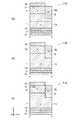
図5は、第1実施形態の変形例に係る半導体装置の一部を表す断面図である。
図6は、第1実施形態の変形例に係る半導体装置の特性を表すグラフである。
図7は、第2実施形態に係る半導体装置を表す斜視断面図である。
第2実施形態に係る半導体装置200は、ゲート電極20の構造について、半導体装置100と差異を有する。
図8は、第3実施形態に係る半導体装置を表す斜視断面図である。
第3実施形態に係る半導体装置300は、n形バリア領域9(第9半導体領域)をさらに有する。n形バリア領域9は、X方向において複数設けられている。複数のn形バリア領域9は、それぞれ、Z方向において、第1部分1aと複数のp形ベース領域3との間に設けられている。
図9は、第4実施形態に係る半導体装置を表す斜視断面図である。
図9に表したように、複数のゲート電極20は、ゲート電極20a、ゲート電極20b、及びゲート電極20cを含む。複数のゲート絶縁層21は、ゲート絶縁層21a、ゲート絶縁層21b、及びゲート絶縁層21cを含む。
また、各半導体領域における不純物濃度については、例えば、SIMS(二次イオン質量分析法)により測定することが可能である。
Claims (11)
- 第1部分と、第2部分と、第1方向において前記第1部分と前記第2部分との間に位置する第3部分と、を有する第1導電形の第1半導体領域と、
前記第1部分の下に設けられた第2導電形の第2半導体領域と、
前記第1部分の上に設けられた第2導電形の第3半導体領域であって、前記第2半導体領域から前記第3半導体領域に向かう第2方向は前記第1方向に対して垂直である、前記第3半導体領域と、
前記第3半導体領域の上に設けられた第1導電形の第4半導体領域と、
前記第1方向において、前記第1半導体領域の一部、前記第3半導体領域、及び前記第4半導体領域の少なくとも一部とゲート絶縁層を介して対向するゲート電極と、
前記第2部分の下に設けられた第1導電形の第5半導体領域と、
前記第2部分の上に設けられた第2導電形の第6半導体領域と、
前記第3部分の上に設けられた第2導電形の第7半導体領域と、
前記第3半導体領域、前記第6半導体領域、及び前記第7半導体領域を囲む第2導電形の第8半導体領域であって、前記第8半導体領域は、
前記第1方向及び前記第2方向に垂直な第3方向において、一部が前記第3半導体領域と並ぶ第1領域と、
前記第3方向において、一部が前記第7半導体領域と並ぶ第2領域と、
を有し、前記第2領域の下端は前記第1領域の下端よりも上方に位置する、前記第8半導体領域と、
を備えた半導体装置。 - 前記第2領域における第2導電形の不純物濃度は、前記第1領域における第2導電形の不純物濃度よりも低い請求項1記載の半導体装置。
- 複数の前記ゲート電極を備え、
複数の前記ゲート電極の1つは、前記第1方向において、前記第7半導体領域と前記複数のゲート電極の別の1つとの間に位置し、
前記複数のゲート電極の前記1つの下端は、前記複数のゲート電極の前記別の1つの下端よりも上方に位置している請求項1または2に記載の半導体装置。 - 前記第1方向において前記第7半導体領域と第1絶縁層を介して対向し、前記第2電極と電気的に接続された第1導電部をさらに備え、
前記第1導電部の下端は、前記複数のゲート電極のそれぞれの下端よりも上方に位置している請求項3記載の半導体装置。 - 前記第1導電部と、前記第1導電部と隣り合う前記ゲート電極と、の間の前記第1方向における距離は、隣り合う前記ゲート電極同士の間の前記第1方向における距離よりも短い請求項4記載の半導体装置。
- 隣り合う前記ゲート電極同士の間の前記第1方向における距離は、前記第1導電部に近づくほど短い請求項4または5に記載の半導体装置。
- 複数の前記第3半導体領域と、
第1導電形の複数の第9半導体領域と、
を備え、
前記複数の第9半導体領域は、それぞれ、前記複数の第3半導体領域と前記第1部分との間に設けられ、
前記複数の第9半導体領域のそれぞれにおける第1導電形の不純物濃度は、前記第1半導体領域における第1導電形の不純物濃度よりも高く、
前記複数の第9半導体領域の1つの前記第1方向における位置は、前記第7半導体領域の前記第1方向における位置と、前記複数の第3半導体領域の別の1つの前記第1方向における位置と、の間にあり、
前記複数の第9半導体領域の前記1つにおける第1導電形の不純物濃度は、前記複数の第9半導体領域の前記別の1つにおける第1導電形の不純物濃度よりも低い請求項1〜6のいずれか1つに記載の半導体装置。 - 第1部分と、第2部分と、第1方向において前記第1部分と前記第2部分との間に位置する第3部分と、を有する第1導電形の第1半導体領域と、
前記第1部分の下に設けられた第2導電形の第2半導体領域と、
前記第1部分の上に設けられた第2導電形の第3半導体領域であって、前記第2半導体領域から前記第3半導体領域に向かう第2方向は前記第1方向に対して垂直である、前記第3半導体領域と、
前記第3半導体領域の上に設けられた第1導電形の第4半導体領域と、
前記第1方向において、前記第1半導体領域の一部、前記第3半導体領域、及び前記第4半導体領域の少なくとも一部とゲート絶縁層を介して対向するゲート電極と、
前記第2部分の下に設けられた第1導電形の第5半導体領域と、
前記第2部分の上に設けられた第2導電形の第6半導体領域と、
前記第3部分の上に設けられた第2導電形の第7半導体領域と、
前記第3半導体領域、前記第6半導体領域、及び前記第7半導体領域を囲む第2導電形の第8半導体領域であって、前記第8半導体領域は、
前記第1方向及び前記第2方向に垂直な第3方向において、一部が前記第3半導体領域と並ぶ第1領域と、
前記第3方向において、一部が前記第7半導体領域と並ぶ第2領域と、
を有し、前記第2領域における第2導電形の不純物濃度は、前記第1領域における第2導電形の不純物濃度よりも高い、前記第8半導体領域と、
を備えた半導体装置。 - 第1部分と、第2部分と、第1方向において前記第1部分と前記第2部分との間に位置する第3部分と、を有する第1導電形の第1半導体領域と、
前記第1部分の下に設けられた第2導電形の第2半導体領域と、
前記第1部分の上に設けられた第2導電形の複数の第3半導体領域であって、前記第2半導体領域から前記複数の第3半導体領域に向かう第2方向は前記第1方向に対して垂直である、前記複数の第3半導体領域と、
前記複数の第3半導体領域の1つの上に設けられた第1導電形の第4半導体領域と、
前記第1方向において、前記第1半導体領域の一部、前記複数の第3半導体領域の前記1つ、及び前記第4半導体領域の少なくとも一部とゲート絶縁層を介して対向するゲート電極と、
前記第2部分の下に設けられた第1導電形の第5半導体領域と、
前記第2部分の上に設けられた第2導電形の第6半導体領域と、
前記第3部分の上に設けられた第2導電形の第7半導体領域と、
前記複数の第3半導体領域、前記第6半導体領域、及び前記第7半導体領域を囲む第2導電形の第8半導体領域と、
複数の第9半導体領域であって、前記複数の第9半導体領域はそれぞれ前記複数の第3半導体領域と前記第1部分との間に設けられ、前記複数の第9半導体領域のそれぞれにおける第1導電形の不純物濃度は、前記第1半導体領域における第1導電形の不純物濃度よりも高く、前記複数の第9半導体領域の1つの前記第1方向における位置は、前記第7半導体領域の前記第1方向における位置と、前記複数の第3半導体領域の別の1つの前記第1方向における位置と、の間にあり、前記複数の第9半導体領域の前記1つにおける第1導電形の不純物濃度は、前記複数の第9半導体領域の前記別の1つにおける第1導電形の不純物濃度よりも低い、前記複数の第9半導体領域と、
を備えた半導体装置。 - 第1部分と、第2部分と、第1方向において前記第1部分と前記第2部分との間に位置する第3部分と、を有する第1導電形の第1半導体領域と、
前記第1部分の下に設けられた第2導電形の第2半導体領域と、
前記第1部分の上に設けられた第2導電形の第3半導体領域であって、前記第2半導体領域から前記第3半導体領域に向かう第2方向は前記第1方向に対して垂直である、前記第3半導体領域と、
前記第3半導体領域の上に設けられた第1導電形の第4半導体領域と、
前記第1方向において、前記第1半導体領域の一部、前記第3半導体領域、及び前記第4半導体領域の少なくとも一部とゲート絶縁層を介して対向するゲート電極と、
前記第2部分の下に設けられた第1導電形の第5半導体領域と、
前記第2部分の上に設けられた第2導電形の第6半導体領域と、
前記第3部分の上に設けられた第2導電形の第7半導体領域と、
前記第1方向において、前記第7半導体領域と第1絶縁層を介して対向する第1導電部であって、前記第1導電部の下端は前記ゲート電極の下端よりも上方に位置する、前記第1導電部と、
前記第3半導体領域、前記第6半導体領域、及び前記第7半導体領域を囲む第2導電形の第8半導体領域と、
を備えた半導体装置。 - 第1部分と、第2部分と、第1方向において前記第1部分と前記第2部分との間に位置する第3部分と、を有する第1導電形の第1半導体領域と、
前記第1部分の下に設けられた第2導電形の第2半導体領域と、
前記第1部分の上に設けられた第2導電形の第3半導体領域であって、前記第2半導体領域から前記第3半導体領域に向かう第2方向は前記第1方向に対して垂直である、前記第3半導体領域と、
前記第3半導体領域の上に設けられた第1導電形の第4半導体領域と、
複数のゲート電極であって、前記複数のゲート電極の1つは、前記第1方向において、前記第1半導体領域の一部、前記第3半導体領域、及び前記第4半導体領域の少なくとも一部とゲート絶縁層を介して対向する、前記複数のゲート電極と、
前記第2部分の下に設けられた第1導電形の第5半導体領域と、
前記第2部分の上に設けられた第2導電形の第6半導体領域と、
前記第3部分の上に設けられた第2導電形の第7半導体領域と、
前記第1方向において前記第7半導体領域と第1絶縁層を介して対向する第1導電部であって、前記第1導電部と、前記第1方向において前記第1導電部と隣り合う前記複数のゲート電極の1つと、の間の距離は、前記第1方向において隣り合う前記ゲート電極同士の間の距離よりも短い、前記第1導電部と、
前記第3半導体領域、前記第6半導体領域、及び前記第7半導体領域を囲む第2導電形の第8半導体領域と、
を備えた半導体装置。
Priority Applications (3)
| Application Number | Priority Date | Filing Date | Title |
|---|---|---|---|
| JP2018029695A JP2019145708A (ja) | 2018-02-22 | 2018-02-22 | 半導体装置 |
| US16/029,799 US10727225B2 (en) | 2018-02-22 | 2018-07-09 | IGBT semiconductor device |
| CN201810767250.6A CN110190053A (zh) | 2018-02-22 | 2018-07-13 | 半导体装置 |
Applications Claiming Priority (1)
| Application Number | Priority Date | Filing Date | Title |
|---|---|---|---|
| JP2018029695A JP2019145708A (ja) | 2018-02-22 | 2018-02-22 | 半導体装置 |
Publications (2)
| Publication Number | Publication Date |
|---|---|
| JP2019145708A true JP2019145708A (ja) | 2019-08-29 |
| JP2019145708A5 JP2019145708A5 (ja) | 2020-03-19 |
Family
ID=67618164
Family Applications (1)
| Application Number | Title | Priority Date | Filing Date |
|---|---|---|---|
| JP2018029695A Pending JP2019145708A (ja) | 2018-02-22 | 2018-02-22 | 半導体装置 |
Country Status (3)
| Country | Link |
|---|---|
| US (1) | US10727225B2 (ja) |
| JP (1) | JP2019145708A (ja) |
| CN (1) | CN110190053A (ja) |
Cited By (1)
| Publication number | Priority date | Publication date | Assignee | Title |
|---|---|---|---|---|
| US11575001B2 (en) | 2020-10-01 | 2023-02-07 | Mitsubishi Electric Corporation | Semiconductor device |
Families Citing this family (8)
| Publication number | Priority date | Publication date | Assignee | Title |
|---|---|---|---|---|
| US9171843B2 (en) | 2013-08-02 | 2015-10-27 | Taiwan Semiconductor Manufacturing Company, Ltd. | Semiconductor device and fabricating the same |
| US11393812B2 (en) * | 2017-12-28 | 2022-07-19 | Fuji Electric Co., Ltd. | Semiconductor device and method of manufacturing semiconductor device |
| JP6935351B2 (ja) * | 2018-03-20 | 2021-09-15 | 株式会社東芝 | 半導体装置 |
| JP7250473B2 (ja) * | 2018-10-18 | 2023-04-03 | 三菱電機株式会社 | 半導体装置 |
| JP7101593B2 (ja) * | 2018-10-30 | 2022-07-15 | 三菱電機株式会社 | 半導体装置 |
| DE102019133030B4 (de) * | 2019-12-04 | 2023-05-04 | Infineon Technologies Austria Ag | Bipolartransistor mit isoliertem gate enthaltende halbleitervorrichtung und herstellungsverfahren |
| JP7403401B2 (ja) * | 2020-07-10 | 2023-12-22 | 三菱電機株式会社 | 半導体装置 |
| JP2022116567A (ja) * | 2021-01-29 | 2022-08-10 | 株式会社東芝 | 半導体装置 |
Citations (3)
| Publication number | Priority date | Publication date | Assignee | Title |
|---|---|---|---|---|
| JP2009021557A (ja) * | 2007-06-14 | 2009-01-29 | Denso Corp | 半導体装置 |
| JP2017098359A (ja) * | 2015-11-20 | 2017-06-01 | トヨタ自動車株式会社 | 逆導通igbt |
| JP2017224685A (ja) * | 2016-06-14 | 2017-12-21 | 株式会社デンソー | 半導体装置 |
Family Cites Families (12)
| Publication number | Priority date | Publication date | Assignee | Title |
|---|---|---|---|---|
| JP5664029B2 (ja) | 2010-09-01 | 2015-02-04 | 株式会社デンソー | 半導体装置 |
| US8716746B2 (en) * | 2010-08-17 | 2014-05-06 | Denso Corporation | Semiconductor device |
| JP5321669B2 (ja) * | 2010-11-25 | 2013-10-23 | 株式会社デンソー | 半導体装置 |
| US9064711B2 (en) | 2011-06-09 | 2015-06-23 | Toyota Jidosha Kabushiki Kaisha | Semiconductor device and method for fabricating semiconductor device |
| JP5787853B2 (ja) * | 2012-09-12 | 2015-09-30 | 株式会社東芝 | 電力用半導体装置 |
| KR20140038750A (ko) * | 2012-09-21 | 2014-03-31 | 삼성전자주식회사 | 반도체 장치 및 그 제조 방법 |
| JP2013145903A (ja) * | 2013-02-28 | 2013-07-25 | Toshiba Corp | 半導体装置 |
| JP2015176927A (ja) * | 2014-03-13 | 2015-10-05 | 株式会社東芝 | 半導体装置および絶縁ゲート型バイポーラトランジスタ |
| JP2016058654A (ja) * | 2014-09-11 | 2016-04-21 | 株式会社東芝 | 半導体装置 |
| JP6597102B2 (ja) * | 2015-09-16 | 2019-10-30 | 富士電機株式会社 | 半導体装置 |
| JP7325167B2 (ja) * | 2017-03-16 | 2023-08-14 | 富士電機株式会社 | 半導体装置の製造方法 |
| JP2018182254A (ja) * | 2017-04-21 | 2018-11-15 | ルネサスエレクトロニクス株式会社 | 半導体装置およびその製造方法 |
-
2018
- 2018-02-22 JP JP2018029695A patent/JP2019145708A/ja active Pending
- 2018-07-09 US US16/029,799 patent/US10727225B2/en active Active
- 2018-07-13 CN CN201810767250.6A patent/CN110190053A/zh active Pending
Patent Citations (3)
| Publication number | Priority date | Publication date | Assignee | Title |
|---|---|---|---|---|
| JP2009021557A (ja) * | 2007-06-14 | 2009-01-29 | Denso Corp | 半導体装置 |
| JP2017098359A (ja) * | 2015-11-20 | 2017-06-01 | トヨタ自動車株式会社 | 逆導通igbt |
| JP2017224685A (ja) * | 2016-06-14 | 2017-12-21 | 株式会社デンソー | 半導体装置 |
Cited By (1)
| Publication number | Priority date | Publication date | Assignee | Title |
|---|---|---|---|---|
| US11575001B2 (en) | 2020-10-01 | 2023-02-07 | Mitsubishi Electric Corporation | Semiconductor device |
Also Published As
| Publication number | Publication date |
|---|---|
| CN110190053A (zh) | 2019-08-30 |
| US20190259747A1 (en) | 2019-08-22 |
| US10727225B2 (en) | 2020-07-28 |
Similar Documents
| Publication | Publication Date | Title |
|---|---|---|
| JP2019145708A (ja) | 半導体装置 | |
| CN108417614B (zh) | 半导体装置 | |
| US11195941B2 (en) | Semiconductor device | |
| JP6392133B2 (ja) | 半導体装置 | |
| JP6445952B2 (ja) | 半導体装置 | |
| JP5768028B2 (ja) | 半導体装置 | |
| CN110310990B (zh) | 半导体装置 | |
| JP2018049908A (ja) | 半導体装置及びその製造方法 | |
| JP6526579B2 (ja) | 半導体装置 | |
| JP2018049866A (ja) | 半導体装置 | |
| JP7204544B2 (ja) | 半導体装置 | |
| JP6588774B2 (ja) | 半導体装置 | |
| JP2019145646A (ja) | 半導体装置 | |
| JP2017157673A (ja) | 半導体装置 | |
| JP2022138939A (ja) | 半導体装置 | |
| US11322585B2 (en) | Semiconductor device | |
| JP7243795B2 (ja) | 半導体装置 | |
| JP6445990B2 (ja) | 半導体装置 | |
| WO2021049351A1 (ja) | 半導体装置 | |
| JP2017037965A (ja) | 半導体装置 | |
| JP2024029584A (ja) | 半導体装置及びその製造方法 | |
| JP2024024290A (ja) | 半導体装置 | |
| JP2023141092A (ja) | 半導体装置 | |
| JP2023045165A (ja) | 半導体装置 | |
| JP2023130809A (ja) | 半導体装置及び半導体パッケージ |
Legal Events
| Date | Code | Title | Description |
|---|---|---|---|
| A521 | Request for written amendment filed |
Free format text: JAPANESE INTERMEDIATE CODE: A523 Effective date: 20200206 |
|
| A621 | Written request for application examination |
Free format text: JAPANESE INTERMEDIATE CODE: A621 Effective date: 20200206 |
|
| A977 | Report on retrieval |
Free format text: JAPANESE INTERMEDIATE CODE: A971007 Effective date: 20201222 |
|
| A131 | Notification of reasons for refusal |
Free format text: JAPANESE INTERMEDIATE CODE: A131 Effective date: 20201224 |
|
| A02 | Decision of refusal |
Free format text: JAPANESE INTERMEDIATE CODE: A02 Effective date: 20210624 |