WO2012014700A1 - パターン形成方法及びポリマーアロイ下地材料 - Google Patents
パターン形成方法及びポリマーアロイ下地材料 Download PDFInfo
- Publication number
- WO2012014700A1 WO2012014700A1 PCT/JP2011/066222 JP2011066222W WO2012014700A1 WO 2012014700 A1 WO2012014700 A1 WO 2012014700A1 JP 2011066222 W JP2011066222 W JP 2011066222W WO 2012014700 A1 WO2012014700 A1 WO 2012014700A1
- Authority
- WO
- WIPO (PCT)
- Prior art keywords
- polymer
- phase
- pattern
- self
- surface layer
- Prior art date
- Legal status (The legal status is an assumption and is not a legal conclusion. Google has not performed a legal analysis and makes no representation as to the accuracy of the status listed.)
- Ceased
Links
Images


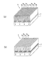

Classifications
-
- H—ELECTRICITY
- H10—SEMICONDUCTOR DEVICES; ELECTRIC SOLID-STATE DEVICES NOT OTHERWISE PROVIDED FOR
- H10P—GENERIC PROCESSES OR APPARATUS FOR THE MANUFACTURE OR TREATMENT OF DEVICES COVERED BY CLASS H10
- H10P76/00—Manufacture or treatment of masks on semiconductor bodies, e.g. by lithography or photolithography
- H10P76/20—Manufacture or treatment of masks on semiconductor bodies, e.g. by lithography or photolithography of masks comprising organic materials
- H10P76/204—Manufacture or treatment of masks on semiconductor bodies, e.g. by lithography or photolithography of masks comprising organic materials of organic photoresist masks
- H10P76/2041—Photolithographic processes
-
- B—PERFORMING OPERATIONS; TRANSPORTING
- B81—MICROSTRUCTURAL TECHNOLOGY
- B81C—PROCESSES OR APPARATUS SPECIALLY ADAPTED FOR THE MANUFACTURE OR TREATMENT OF MICROSTRUCTURAL DEVICES OR SYSTEMS
- B81C1/00—Manufacture or treatment of devices or systems in or on a substrate
- B81C1/00015—Manufacture or treatment of devices or systems in or on a substrate for manufacturing microsystems
- B81C1/00023—Manufacture or treatment of devices or systems in or on a substrate for manufacturing microsystems without movable or flexible elements
- B81C1/00031—Regular or irregular arrays of nanoscale structures, e.g. etch mask layer
-
- B—PERFORMING OPERATIONS; TRANSPORTING
- B82—NANOTECHNOLOGY
- B82Y—SPECIFIC USES OR APPLICATIONS OF NANOSTRUCTURES; MEASUREMENT OR ANALYSIS OF NANOSTRUCTURES; MANUFACTURE OR TREATMENT OF NANOSTRUCTURES
- B82Y10/00—Nanotechnology for information processing, storage or transmission, e.g. quantum computing or single electron logic
-
- B—PERFORMING OPERATIONS; TRANSPORTING
- B82—NANOTECHNOLOGY
- B82Y—SPECIFIC USES OR APPLICATIONS OF NANOSTRUCTURES; MEASUREMENT OR ANALYSIS OF NANOSTRUCTURES; MANUFACTURE OR TREATMENT OF NANOSTRUCTURES
- B82Y40/00—Manufacture or treatment of nanostructures
-
- G—PHYSICS
- G03—PHOTOGRAPHY; CINEMATOGRAPHY; ANALOGOUS TECHNIQUES USING WAVES OTHER THAN OPTICAL WAVES; ELECTROGRAPHY; HOLOGRAPHY
- G03F—PHOTOMECHANICAL PRODUCTION OF TEXTURED OR PATTERNED SURFACES, e.g. FOR PRINTING, FOR PROCESSING OF SEMICONDUCTOR DEVICES; MATERIALS THEREFOR; ORIGINALS THEREFOR; APPARATUS SPECIALLY ADAPTED THEREFOR
- G03F7/00—Photomechanical, e.g. photolithographic, production of textured or patterned surfaces, e.g. printing surfaces; Materials therefor, e.g. comprising photoresists; Apparatus specially adapted therefor
- G03F7/0002—Lithographic processes using patterning methods other than those involving the exposure to radiation, e.g. by stamping
-
- G—PHYSICS
- G03—PHOTOGRAPHY; CINEMATOGRAPHY; ANALOGOUS TECHNIQUES USING WAVES OTHER THAN OPTICAL WAVES; ELECTROGRAPHY; HOLOGRAPHY
- G03F—PHOTOMECHANICAL PRODUCTION OF TEXTURED OR PATTERNED SURFACES, e.g. FOR PRINTING, FOR PROCESSING OF SEMICONDUCTOR DEVICES; MATERIALS THEREFOR; ORIGINALS THEREFOR; APPARATUS SPECIALLY ADAPTED THEREFOR
- G03F7/00—Photomechanical, e.g. photolithographic, production of textured or patterned surfaces, e.g. printing surfaces; Materials therefor, e.g. comprising photoresists; Apparatus specially adapted therefor
- G03F7/26—Processing photosensitive materials; Apparatus therefor
- G03F7/40—Treatment after imagewise removal, e.g. baking
- G03F7/405—Treatment with inorganic or organometallic reagents after imagewise removal
-
- G—PHYSICS
- G03—PHOTOGRAPHY; CINEMATOGRAPHY; ANALOGOUS TECHNIQUES USING WAVES OTHER THAN OPTICAL WAVES; ELECTROGRAPHY; HOLOGRAPHY
- G03F—PHOTOMECHANICAL PRODUCTION OF TEXTURED OR PATTERNED SURFACES, e.g. FOR PRINTING, FOR PROCESSING OF SEMICONDUCTOR DEVICES; MATERIALS THEREFOR; ORIGINALS THEREFOR; APPARATUS SPECIALLY ADAPTED THEREFOR
- G03F7/00—Photomechanical, e.g. photolithographic, production of textured or patterned surfaces, e.g. printing surfaces; Materials therefor, e.g. comprising photoresists; Apparatus specially adapted therefor
- G03F7/26—Processing photosensitive materials; Apparatus therefor
- G03F7/42—Stripping or agents therefor
- G03F7/427—Stripping or agents therefor using plasma means only
-
- H—ELECTRICITY
- H10—SEMICONDUCTOR DEVICES; ELECTRIC SOLID-STATE DEVICES NOT OTHERWISE PROVIDED FOR
- H10P—GENERIC PROCESSES OR APPARATUS FOR THE MANUFACTURE OR TREATMENT OF DEVICES COVERED BY CLASS H10
- H10P50/00—Etching of wafers, substrates or parts of devices
- H10P50/69—Etching of wafers, substrates or parts of devices using masks for semiconductor materials
- H10P50/691—Etching of wafers, substrates or parts of devices using masks for semiconductor materials for Group V materials or Group III-V materials
- H10P50/692—Etching of wafers, substrates or parts of devices using masks for semiconductor materials for Group V materials or Group III-V materials characterised by their composition, e.g. multilayer masks or materials
-
- H—ELECTRICITY
- H10—SEMICONDUCTOR DEVICES; ELECTRIC SOLID-STATE DEVICES NOT OTHERWISE PROVIDED FOR
- H10P—GENERIC PROCESSES OR APPARATUS FOR THE MANUFACTURE OR TREATMENT OF DEVICES COVERED BY CLASS H10
- H10P76/00—Manufacture or treatment of masks on semiconductor bodies, e.g. by lithography or photolithography
- H10P76/40—Manufacture or treatment of masks on semiconductor bodies, e.g. by lithography or photolithography of masks comprising inorganic materials
- H10P76/408—Manufacture or treatment of masks on semiconductor bodies, e.g. by lithography or photolithography of masks comprising inorganic materials characterised by their sizes, orientations, dispositions, behaviours or shapes
- H10P76/4085—Manufacture or treatment of masks on semiconductor bodies, e.g. by lithography or photolithography of masks comprising inorganic materials characterised by their sizes, orientations, dispositions, behaviours or shapes characterised by the processes involved to create the masks
-
- B—PERFORMING OPERATIONS; TRANSPORTING
- B81—MICROSTRUCTURAL TECHNOLOGY
- B81C—PROCESSES OR APPARATUS SPECIALLY ADAPTED FOR THE MANUFACTURE OR TREATMENT OF MICROSTRUCTURAL DEVICES OR SYSTEMS
- B81C2201/00—Manufacture or treatment of microstructural devices or systems
- B81C2201/01—Manufacture or treatment of microstructural devices or systems in or on a substrate
- B81C2201/0101—Shaping material; Structuring the bulk substrate or layers on the substrate; Film patterning
- B81C2201/0147—Film patterning
- B81C2201/0149—Forming nanoscale microstructures using auto-arranging or self-assembling material
Definitions
- Embodiments of the present invention relate to a pattern formation method and a polymer alloy base material.
- a self-assembled monolayer is formed on a substrate, a photoresist is applied thereon, a line-and-space resist pattern is formed by lithography, and oxygen is used with the resist pattern as a mask.
- a part of the SAM is chemically modified by selectively irradiating with X-rays in an atmosphere, the resist pattern is removed, and a block copolymer is coated on the SAM and annealed to form a microphase separation pattern of the block copolymer.
- the method is known.
- a block copolymer is formed by forming a SAM on a substrate, selectively exposing a part of the SAM by interference exposure to form a chemically modified dot pattern, applying a block copolymer on the SAM, and annealing.
- a method of forming a microphase separation pattern is known.
- a monomolecular film made of a polymer compound called a polymer brush is formed on a substrate by heat treatment for a long time, and a photoresist is applied thereon to form a line-and-space resist pattern by lithography.
- the resist pattern is used as a mask to selectively irradiate X-rays in an oxygen atmosphere to remove part of the polymer brush, remove the resist pattern, apply a block copolymer on the polymer brush, and anneal to block.
- Methods for forming microphase separation patterns of copolymers are known.
- a polymer brush is formed on the substrate, an electron beam resist is applied on the substrate, a dot pattern is formed by lithography, and oxygen plasma is irradiated using the dot pattern of the electron beam resist as a mask to partially remove the polymer brush.
- a method of forming a microphase separation pattern of a block copolymer by removing the resist pattern, applying a block copolymer on the SAM, and annealing it is disclosed that the dot pitch of the dot pattern of the block copolymer can be narrower than the dot pitch of the dot pattern formed on the electron beam resist.
- the surface free energy can be controlled more stably than SAM composed of a silane coupling agent.
- the hydroxyl group at the end of the polymer must sufficiently cause a chemical reaction with the surface of the Si substrate, and the hydroxyl group is sufficiently diffused in the vicinity of Si at a temperature at which the polymer is not thermally decomposed. Since it is necessary to provide heat energy exceeding that, heat treatment for a long time is required, and it is not practical as a microfabrication technique for semiconductor devices and the like.
- An object of the present invention is to provide a pattern forming method and a polymer alloy base material capable of forming a highly oriented phase-separated structure pattern in a polymer alloy in a short time.
- the pattern forming method includes stacking a self-assembled monomolecular film and a polymer film on a substrate and chemically bonding the polymer film and the self-assembled monolayer by irradiating energy rays. Forming a polymer surface layer on the self-assembled monolayer and forming a polymer alloy having a phase separation structure pattern on the polymer surface layer.
- (A)-(c) is a perspective view which shows the pattern formation method of the polymer alloy which concerns on 1st Embodiment.
- (D) is a perspective view which shows the pattern formation method of the polymer alloy which concerns on 1st Embodiment.
- (A)-(c) is a perspective view which shows the pattern formation method of the polymer alloy which concerns on 2nd Embodiment.
- (D) is a perspective view which shows the pattern formation method of the polymer alloy which concerns on 2nd Embodiment.
- (e) is a perspective view which shows the pattern formation method of the polymer alloy which concerns on 2nd Embodiment.
- (A), (b) is a perspective view which shows the pattern formation method of the polymer alloy which concerns on 2nd Embodiment.
- (A), (b) is a perspective view which shows the pattern formation method of the polymer alloy which concerns on 3rd Embodiment.
- FIG. 1A (a) to 1 (c), FIG. 1B (d), and (e) are perspective views showing a polymer alloy pattern forming method according to the first embodiment.
- a self-assembled monolayer 2 is formed on a substrate 1.
- the substrate 1 a silicon wafer, a doped silicon wafer, a silicon wafer having an insulating layer or a metal layer serving as an electrode or wiring formed on the surface, a mask blank, a III-V group compound semiconductor wafer such as GaAs, AlGaAs, or the like is used. Can do. Further, a chromium or chromium oxide deposition substrate, an aluminum deposition substrate, an IBSPG coated substrate, a spin-on-glass (SOG) coated substrate, or a SiN coated substrate can also be used. In particular, the substrate 1 preferably has a number of hydroxy groups on the surface from the viewpoint of easy formation of the self-assembled monolayer 2.
- the self-assembled monomolecular film 2 is preferably made of a material that easily reacts with a hydroxy group on the surface of a metal or metal oxide formed on a silicon substrate, for example, a material containing a silane coupling agent.
- the self-assembled monomolecular film 2 is composed of a photopolymerization initiator that efficiently absorbs energy rays such as ultraviolet rays and electron beams and causes a crosslinking reaction with the polymer in contact, for example, a material having a benzophenone skeleton. It is preferable.
- R in the general formula Ia is a linear alkyl having Si—F, Si—Cl, Si—Br, or Si—OH, Si—OCH 3 , Si—OC 2 H 5 , Si—OC 3 H 7 at the terminal. Group, and may have an ether bond or the like in the alkyl chain.
- the material represented by the general formula Ia contains a benzophenone skeleton, it absorbs energy rays efficiently, and the n-orbital electron of the carbonyl group of benzophenone is excited to the ⁇ * -orbital and reacts with the contacting alkyl chain of the polymer. To do.
- the alkyl chain of the polymer in contact is most likely to react with tertiary carbon. For this reason, the self-assembled monolayer 2 made of the material represented by the general formula Ia and the polymer can be cross-linked by irradiation with energy rays.
- the material of the self-assembled monolayer 2 is preferably a material that is easy to synthesize and low in cost among materials represented by the general formula Ia.
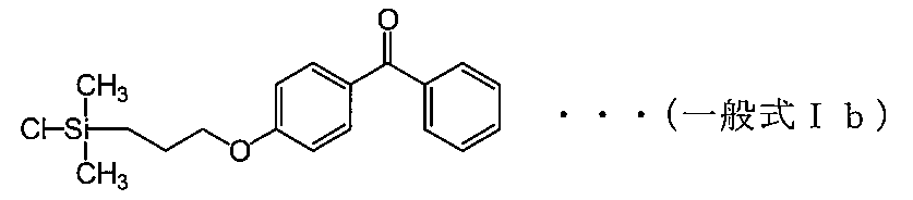
- a silane coupling agent including a benzophenone skeleton represented by the following general formula Ib can be used.
- the self-assembled monolayer 2 spin coating, dip coating, vapor phase growth, doctor blade method, curtain coating, or the like can be used. Before forming the self-assembled monolayer 2, it is preferable to perform a pretreatment such as ultraviolet irradiation on the substrate 1 in order to remove organic impurities attached to the surface of the substrate 1.
- a pretreatment such as ultraviolet irradiation
- the material of the self-assembled monolayer 2 is diluted with a solvent or spin-coated on the substrate 1 as a stock solution, and a hot plate or the like is used if necessary.
- the self-assembled monolayer 2 is formed by baking. Note that the material of the excess self-assembled monolayer 2 adsorbed on the substrate 1 beyond the monolayer is washed away.
- the concentration at which the material of the self-assembled monolayer 2 is diluted with a solvent is preferably 1 to 30 wt%, but is not particularly limited. It is preferable to adjust the concentration in accordance with the degree of spreading of the substrate 1.
- the solvent to be used varies depending on the material of the self-assembled monolayer 2, but a solvent that does not react with the material of the self-assembled monolayer 2 is preferable.
- solvents include aromatic hydrocarbons such as toluene, xylene and mesitylene, cycloalkanes such as cyclohexane, cycloheptane, cyclooctane and cyclononane, alkanes such as hexane, heptane, octane, nonane and decane, methanol, Alkyl alcohols such as ethanol, 1-propanol and 2-propanol can be used.
- organic solvents such as ketones, cellosolves, and esters used for general photoresist solvents can be used from the viewpoints of reactivity, wettability with the substrate 1, and volatility.
- ketones include cyclohexanone, acetone, ethyl methyl ketone, and methyl isobutyl ketone.
- cellosolves include methyl cellosolve, methyl cellosolve acetate, ethyl cellosolve acetate, and butyl cellosolve acetate.
- the esters include ethyl acetate, butyl acetate, isoamyl acetate, ⁇ -butyrolactone, and methyl 3-methoxypropionate.
- Solvents can be used in combination of two or more as required. From the viewpoint of reactivity with the functional group on the surface of the substrate 1, it is preferable to use a dehydrated solvent.
- the temperature at the time of baking on a hot plate or the like is 100 to 200 because the material of the self-assembled monolayer 2 generates energy exceeding the activation energy for chemically bonding with the functional group on the surface of the substrate 1. ° C is preferred.
- the solvent used to wash away (rinse) the material of the extra self-assembled monolayer 2 adsorbed on the substrate 1 beyond the monolayer It is preferable to use the same solvent as used in the above.
- the material of the self-assembled monolayer 2 is diluted with a solvent, and the substrate 1 is immersed in the diluted solution for a certain period of time. A film 2 is formed.
- the concentration at which the material of the self-assembled monolayer 2 is diluted with a solvent is preferably 1 to 30 wt%.
- the solvent to be used is preferably a solvent that does not react with the material of the self-assembled monolayer 2 like the solvent used for spin coating.
- solvents include aromatic hydrocarbons such as toluene, xylene and mesitylene, cycloalkanes such as cyclohexane, cycloheptane, cyclooctane and cyclononane, alkanes such as hexane, heptane, octane, nonane and decane, methanol, Alkyl alcohols such as ethanol, 1-propanol and 2-propanol can be used. From the viewpoint of reactivity with the functional group on the surface of the substrate 1, it is preferable to use a dehydrated solvent.
- the immersion time depends on the concentration, reactivity, etc., but is preferably 1 to 60 minutes.
- the substrate 1 may be immersed by heating the solution.
- the immersion temperature is set to a temperature below the boiling point of the solvent and set so that the material of the self-assembled monolayer 2 does not decompose before reacting with the functional group on the surface of the substrate 1, and is generally adjusted to 40 to 100 ° C. .
- the solvent used to wash away (rinse) the material of the extra self-assembled monolayer 2 adsorbed on the self-assembled monolayer 2 beyond the monolayer is the same as the solvent used for the immersion. It is preferable to use one. After rinsing, it is preferable to blow off an inert gas such as nitrogen or argon to blow off the solvent, and in some cases, heat on a hot plate to remove the solvent.
- an inert gas such as nitrogen or argon
- the material of the self-assembled monolayer 2 is made into a gaseous state by lowering the pressure, raising the temperature, or both, and introducing the substrate 1 into the gas state. Then, the self-assembled monolayer 2 is formed on the surface of the substrate 1 by exposure for a certain time.
- the pressure is lowered or the temperature is raised or both are performed according to the vapor pressure characteristics of the material.
- the material of the excess self-assembled monolayer 2 adsorbed on the substrate 1 beyond the monolayer may be washed away with a solvent.
- a solvent it is preferable to use the same solvent as used in the spin coating described above.
- a polymer film 3 is formed on the self-assembled monomolecular film 2.
- the material of the polymer film 3 is a surface suitable for chemically aligning with the self-assembled monomolecular film 2 by irradiation of high energy rays and adjusting the orientation of the microphase separation structure of the polymer alloy formed on the surface. Use one with energy.
- the substrate 1 is irradiated with high energy rays to chemically bond (crosslink) the polymer film 3 to the self-assembled monomolecular film 2, and the polymer surface layer 4 is self-assembled. Formed on the oxidized monomolecular film 2.
- the energy rays applied to the self-assembled monolayer 2 are not particularly limited as long as the material of the self-assembled monolayer 2 has a wavelength with sensitivity.
- ultraviolet rays mercury lamp i-line, h-line or g-line, xenon lamp light, new ultraviolet light (for example, excimer laser light such as KrF or ArF), X-ray, synchrotron orbital radiation (SR), electron Lines, gamma rays, ion beams, and the like can be used.
- a polymer alloy 5 having a phase separation structure is formed on the polymer surface layer 4.
- the vertical orientation of the phase separation structure of the polymer alloy 5 can be improved as compared with the case where the polymer alloy 5 is directly formed on the self-assembled monolayer 2. it can.
- Polymer alloy 5 is, for example, a block copolymer, a polymer blended with different types of homopolymers, a polymer blended with homopolymers and block copolymers, or a graft copolymer.
- the polymer alloy 5 has a phase separation structure composed of a first phase 5a and a second phase 5b.
- the polymer alloy 5 includes, for example, a block copolymer in which the first phase 5a is made of a polystyrene block chain and the second phase 5b is made of a polybutadiene block chain, or the first phase 5a is made of a polystyrene block chain.
- the second phase 5b is a block copolymer composed of a polymethylmethacrylate block chain.
- the first phase 5a is a block copolymer composed of a polynorbornadiene block chain
- the second phase 5b is composed of a polymethylmethacrylate block chain.
- the first phase 5a and the second phase 5b preferably constitute a lamellar structure.
- the phase separation structure of polymer alloy 5 may be composed of three or more phases.
- the formation method of the polymer alloy 5 is not particularly limited. For example, spin coating, dip coating, doctor blade method, curtain coating, and other methods can be used. After the polymer alloy 5 solution is applied on the polymer surface layer 4, the solvent may be removed by heating on a hot plate if necessary. The heating temperature at this time is preferably 70 to 120 ° C.
- phase-separate the polymer alloy 5 it is generally annealed at a temperature equal to or higher than the glass transition temperature of the polymer alloy 5.
- the phase separation rate of a block copolymer is correlated to the annealing temperature (see, for example, A. M. Welander et al., Macromolecules, 41, 2759-2761, 2008).
- ODT order-disorder transition temperature
- a disordered structure is formed and a phase separation structure cannot be obtained.
- the annealing temperature is preferably 130 to 280 ° C.
- Annealing is performed using an oven or a hot plate. When using an oven, anneal at a low temperature for a long time. When a hot plate is used, annealing is performed at a high temperature for a short time.
- the polymer alloy 5 when annealing is performed in an atmosphere where a reactive gas such as oxygen is present in a minute amount, the polymer alloy 5 may be decomposed when the annealing temperature becomes high. Therefore, from the viewpoint of preventing the decomposition of the polymer alloy 5, it is preferable to anneal in an inert gas atmosphere such as argon or nitrogen. If necessary, annealing may be performed in a forming gas atmosphere containing about 3% hydrogen.
- either one of the first phase 5a and the second phase 5b of the polymer alloy 5 may be selectively removed.
- a line and space pattern can be formed in the polymer alloy 5 by selectively removing one of the first phase 5a and the second phase 5b constituting the lamella structure.
- the polymer alloy 5 is comprised from three or more phases, the one part phase of those phases is removed.
- the first phase 5a and the second phase 5b are required to be composed of block chains that can be selectively removed by any method.
- a block copolymer phase having a block chain of polystyrene and a block copolymer phase having a block chain of polybutadiene can be selectively removed by applying ozone treatment to the block copolymer.
- RIE reactive ion etching
- the polymer alloy 5 is a block copolymer in which the first phase 5a is made of polystyrene block chains and the second phase 5b is made of polybutadiene block chains
- the second phase 5b is treated by ozone treatment. It can be selectively removed leaving only the first phase 5a.
- the polymer alloy 5 is a block copolymer in which the first phase 5a is made of a polystyrene block chain and the second phase 5b is made of a polymethylmethacrylate block chain, or the first phase 5a is a block of polynorbornadiene.
- the second phase 5b is a block copolymer comprising a block chain of polymethyl methacrylate, selectively removing the second phase 5b by RIE using a reactive gas such as O 2, CF 4
- a reactive gas such as O 2, CF 4
- heat treatment or wet etching methods can be used.
- a block copolymer having a polymer chain whose main chain is cleaved by irradiation with energy rays and a polymer chain that is hardly decomposable with respect to energy rays is used as a pattern forming material
- the film is irradiated with light or an electron beam.
- the polymer phase is selectively removed by volatilization by heating or wet etching.
- the first solution is used.
- One of the second phase 5a and the second phase 5b can be selectively removed.
- the developer may be an organic developer or an aqueous developer (alkaline developer).
- Organic developers include alcohols such as methanol, ethanol, and isopropanol, ketones such as cyclohexanone, acetone, ethyl methyl ketone, and methyl isobutyl ketone, cellosolve such as methyl cellosolve, methyl cellosolve acetate, ethyl cellosolve acetate, and butyl cellosolve acetate.
- organic solvents such as ethyl acetate, butyl acetate, isoamyl acetate, ⁇ -butyrolactone, and esters such as methyl 3-methoxypropionate.
- the above-mentioned solvents can be used in combination of two or more as necessary.
- an organic alkaline aqueous solution either an organic alkaline aqueous solution or an inorganic alkaline aqueous solution may be used.
- the organic alkaline aqueous solution include a tetramethylammonium hydroxide aqueous solution, a tetraethylammonium hydroxide aqueous solution, and a choline aqueous solution.
- the inorganic alkaline aqueous solution include a potassium hydroxide aqueous solution and a sodium hydroxide aqueous solution.
- the concentration of the alkaline developer is not limited.
- optional additives can be added to these developers as necessary.
- a surfactant can be added to lower the surface tension of the developer, or a neutral salt can be added to activate development.
- the temperature of the developer is arbitrary, and cold water or hot water can be used.
- the remaining first phase 5a can be used as a mask for etching a base layer, that is, a wafer constituting the substrate 1, a metal layer or an insulating layer on the wafer.
- a monomolecular film of 4- (3′chlorodimethylsilyl) propyloxybenzophenone (CSBP) as a self-assembled monomolecular film 2 is formed on a silicon wafer as a substrate 1, and on that, A polymer film as the polymer film 3 is formed, the CSBP monomolecular film and the polymer film are exposed with an ArF excimer laser to form a polymer surface layer as the polymer surface layer 4, and a block copolymer lamella as the polymer alloy 5 A microphase separation structure was formed.
- CSBP 4- (3′chlorodimethylsilyl) propyloxybenzophenone
- ABP is represented by the following chemical formula.
- CSBP is represented by the following chemical formula.
- a toluene solution of CSBP (2.26 mM, 4 ml) is dropped on the silicon wafer corresponding to the substrate 1, and then a toluene solution of triethylamine (0.247M, 2 ml) is continuously dropped, left for 1 minute, and rotated. The solution was shaken off. Thereafter, the entire surface was rinsed with cyclohexanone, and a polymer solution for the polymer film corresponding to the polymer film 3 was spin-coated thereon. The polymer solution for the polymer film was dissolved in toluene and applied at a rotational speed of 2000 rpm. After coating, the film is baked at 110 ° C. for 90 seconds to form a CSBP self-assembled monomolecular film corresponding to the self-assembled monomolecular film 2 on the silicon wafer, and further, a polymer film corresponding to the polymer film 3 is laminated.
- the polymer solution for the polymer film was adjusted to a concentration of 1 wt%.
- P9225-SMMAran which is a random copolymer (PS-r-PMMA) of polystyrene (PS) and polymethyl methacrylate (PMMA) purchased from Polymer Source, was used.
- P9225-SMMAran has a number average molecular weight (Mn) of 7000, a dispersity (Mw / Mn) of 1.20, and a ratio of the PS moiety to the total molecular weight (f (PS)) of 0.59.
- the prepared polymer film was exposed with an ArF excimer laser at an exposure amount of 10 to 490 mJ / cm 2 . After the exposure, the entire surface of the silicon wafer was rinsed with cyclohexanone to obtain a polymer surface layer corresponding to the polymer surface layer 4.
- P189-SMMA which is a block copolymer (PS-b-PMMA) of polystyrene (PS) and polymethyl methacrylate (PMMA) purchased from Polymer Source, was used.
- P189-SMMA has a PS block and PMMA block having a number average molecular weight (Mn) of 86500 and a dispersity (Mw / Mn) of 1.08.
- Mn number average molecular weight
- Mw / Mn dispersity
- the ratio of the PS moiety to the total molecular weight (f (PS)) is 0.54.
- a polyethylene glycol monomethyl ether acetate (PGMEA) solution of a block copolymer was adjusted to a concentration of 2.0 wt%, spin-coated on a polymer surface layer at a rotation speed of 2000 rpm, and baked on a hot plate at 110 ° C. for 90 seconds to form a polymer alloy.
- a block copolymer corresponding to 5 was formed.
- the block copolymer was phase-separated into a PS phase composed of polystyrene block chains and a PMMA phase composed of polymethylmethacrylate block chains by annealing at 220 ° C. for 1 minute on a hot plate baker in a nitrogen atmosphere.
- NCH-50 silicon chip
- the PMMA phase having a higher etching rate than the PS phase could be selectively removed.
- IPA isopropyl alcohol
- MIBK methyl isobutyl ketone
- the pattern forming method and the forming material of the present embodiment have high controllability of the phase separation structure with respect to the block copolymer.
- the second embodiment is different from the first embodiment in that the polymer alloy 5 is formed after the pattern is formed on the polymer surface layer 4.
- the polymer alloy 5 is formed after the pattern is formed on the polymer surface layer 4.
- a manufacturing method description is abbreviate
- FIGS. 2A (a) to 2 (c), 2B (d), and (e) are perspective views showing a polymer alloy pattern forming method according to the second embodiment.
- a photoresist 6 having a pattern such as line and space is formed on the polymer film 3.
- the polymer surface layer 4 is etched using the photoresist 6 as a mask, and the pattern of the photoresist 6 is transferred to the polymer surface layer 4.
- a polymer alloy 5 having a phase separation structure is formed on the polymer surface layer 4 and the exposed self-assembled monolayer 2.
- the first phase 5a of the polymer alloy 5 is formed on the polymer surface layer 4, and the second phase 5b is formed on the self-assembled monolayer 2 exposed.
- the contact angle of the first phase 5a to the polymer surface layer 4 is smaller than the contact angle to the self-assembled monolayer 2 and the contact angle of the second phase 5b to the self-assembled monolayer 2 is the polymer surface.
- the contact angle with respect to the layer 4 is equal to or smaller than that, or the contact angle with respect to the self-assembled monolayer 2 of the second phase 5b is smaller than the contact angle with respect to the polymer surface layer 4, and the polymer surface layer of the first phase 5a
- the contact angle with respect to 4 is equal to or smaller than the contact angle with respect to the self-assembled monolayer 2
- the first phase 5a is formed on the polymer surface layer 4, and the self-assembled monolayer 2 in which the second phase 5b is exposed. Formed on top.
- either one of the first phase 5a and the second phase 5b of the polymer alloy 5 may be selectively removed.
- the polymer alloy 5 is comprised from three or more phases, the one part phase of those phases is removed.
- the period of the pattern of the phase separation structure of the polymer alloy 5 can be made smaller than the minimum period of the pattern of the photoresist 6 due to the resolution limit of the exposure apparatus.
- a CSBP monomolecular film as a self-assembled monomolecular film 2 is formed on a silicon wafer as a substrate 1, a polymer film as a polymer film 3 is formed thereon, and a CSBP monomolecular film is formed.
- the molecular film and the polymer film are exposed with an ArF excimer laser to form a polymer surface layer as the polymer surface layer 4, and further, a photoresist as a photoresist 6 is laminated, and pattern exposure and development are performed with an ArF excimer laser.
- the polymer surface layer is patterned by reactive ion etching (RIE) using O 2 gas through the resist pattern, and after the resist pattern is peeled off, a lamellar block copolymer as polymer alloy 5 is formed on the pattern of the formed polymer surface layer. A pattern of microphase separation was formed.
- RIE reactive ion etching
- a CSBP toluene solution (2.26 mM, 4 ml) is dropped on a silicon wafer corresponding to the substrate 1, and then a triethylamine toluene solution (0.247M, 2 mL) is continuously dropped.
- the solution was shaken off. Thereafter, the entire surface was rinsed with cyclohexanone, and a polymer solution for the polymer film corresponding to the polymer film 3 was spin-coated thereon.
- the polymer solution for the polymer film was dissolved in toluene and applied at a rotational speed of 2000 rpm. After coating, the film is baked at 110 ° C. for 90 seconds to form a CSBP self-assembled monomolecular film corresponding to the self-assembled monomolecular film 2 on the silicon wafer, and further, a polymer film corresponding to the polymer film 3 is laminated.
- polystyrene (PS) P1071-St, P8007-S, and P8096-S purchased from Polymer Source were used.
- P1071-St, P8007-S, and P8096-S have number average molecular weights (Mn) of 115900, 30000, and 8000, and dispersities (Mw / Mn) of 1.04, 1.07, and 1.06PS, respectively.
- the ratio to molecular weight (f (PS)) is 0.59.
- concentration of the polymer solution using P1071-St, P8007-S, and P8096-S was 1.0 wt%.
- the produced polymer film was exposed with an ArF excimer laser at an exposure amount of 490 mJ / cm 2 . After the exposure, the entire surface of the silicon wafer was rinsed with cyclohexanone to obtain a polymer surface layer corresponding to the polymer surface layer 4.
- a photoresist corresponding to the photoresist 6 was spin-coated on the produced polymer surface layer.
- AR1687 purchased from JSR Corporation was used as the photoresist.
- the photoresist was pattern-exposed with an ArF excimer laser.
- line and space (1: 1) patterns of half pitches 100, 95, 90, 85, 80, 75, 70, and 65 nm were transferred.
- the exposure was 25.5 mJ / cm 2 .
- development was performed with a 2.38% tetramethylammonium hydroxide aqueous solution (AD-10) purchased from Tama Chemical Co., Ltd. and line pitches of half pitch 100, 95, 90, 85, 80, 75, 70, 65 nm
- a space (1: 1) pattern was formed on each photoresist.
- O2 plasma etching was performed with an inductively coupled reactive etching apparatus (ICP-RIE). Coil Power and Platen Power were performed at 10 and 10 W for 2 minutes, respectively, and the polymer surface layer was removed using the photoresist as a mask. Thereafter, the photoresist is removed by rinsing with cyclohexanone for 1 minute, and line and space (1: 1) patterns of half pitch 100, 95, 90, 85, 80, 75, 70, 65 nm are respectively formed on the polymer surface layer. Formed.
- ICP-RIE inductively coupled reactive etching apparatus
- P189-SMMA which is a block copolymer (PS-b-PMMA) of polystyrene (PS) and polymethyl methacrylate (PMMA) purchased from Polymer Source, was used.
- P189-SMMA has a PS block and PMMA block having a number average molecular weight (Mn) of 86500 and a dispersity (Mw / Mn) of 1.08.
- Mn number average molecular weight
- Mw / Mn dispersity
- the ratio of the PS moiety to the total molecular weight (f (PS)) is 0.54.
- a polyethylene glycol monomethyl ether acetate (PGMEA) solution of a block copolymer was adjusted to a concentration of 2.0 wt%, spin-coated on a polymer surface layer at a rotation speed of 2000 rpm, and baked on a hot plate at 110 ° C. for 90 seconds to form a polymer alloy.
- a block copolymer corresponding to 5 was formed.
- the block copolymer was phase-separated into a PS phase composed of polystyrene block chains and a PMMA phase composed of polymethyl methacrylate block chains by annealing in a nitrogen atmosphere.
- Phases obtained by measuring a 500 nm ⁇ 500 nm (500 nm ⁇ ) region of each sample surface with an atomic force microscope (Nanoscope III) using a silicon chip [NCH-50] as a cantilever and in a tapping mode. The pattern orientation of the lamellar microdomain structure was evaluated from the images.
- the PMMA phase having an etching rate higher than that of the PS phase could be selectively removed.
- IPA isopropyl alcohol
- MIBK methyl isobutyl ketone
- the third embodiment is different from the second embodiment in the pattern forming method of the polymer surface layer 4.
- description is abbreviate
- FIGS. 4A and 4B are perspective views showing a polymer alloy pattern forming method according to the third embodiment.
- the polymer film 3 and the self-assembled monomolecular film 2 thereunder are subjected to pattern exposure using high energy rays, and the polymer film 3 in the region irradiated with the high energy rays is exposed.
- the self-assembled monolayer 2 are chemically bonded (crosslinked) to form a polymer surface layer 4 on the self-assembled monolayer 2. That is, a high energy ray is irradiated to a partial region (pattern region) on the substrate 1, and the polymer film 3 and the self-assembled monolayer 2 in the partial region are selectively chemically bonded to form a polymer surface layer. 4 is formed.
- the polymer film 3 is selectively removed leaving the polymer surface layer 4.
- the period of the pattern of the phase separation structure of the polymer alloy 5 is defined as the minimum period of the pattern of the polymer surface layer 4 due to the limit of resolution of the high energy beam used for pattern exposure of the polymer film 3 and the self-assembled monolayer 2. Can be made smaller.
- a polymer alloy is formed on a self-assembled monolayer through a polymer surface layer, whereby a highly oriented phase separation structure pattern can be formed in a polymer alloy in a short time. Can be formed. Further, by selectively removing a part of the phase separation structure, the polymer alloy can be used as an etching mask having a fine pattern.
- the present invention is not limited to the first to third embodiments, and various modifications can be made without departing from the spirit of the invention. Further, the process order of the pattern forming methods shown in the first to third embodiments is not limited to the above.
Landscapes
- Engineering & Computer Science (AREA)
- Chemical & Material Sciences (AREA)
- Nanotechnology (AREA)
- Physics & Mathematics (AREA)
- Manufacturing & Machinery (AREA)
- General Physics & Mathematics (AREA)
- Crystallography & Structural Chemistry (AREA)
- Analytical Chemistry (AREA)
- Microelectronics & Electronic Packaging (AREA)
- Mathematical Physics (AREA)
- Theoretical Computer Science (AREA)
- Condensed Matter Physics & Semiconductors (AREA)
- Plasma & Fusion (AREA)
- Inorganic Chemistry (AREA)
- Organic Chemistry (AREA)
- Exposure Of Semiconductors, Excluding Electron Or Ion Beam Exposure (AREA)
- Photosensitive Polymer And Photoresist Processing (AREA)
- Materials For Photolithography (AREA)
- Formation Of Insulating Films (AREA)
Abstract
[課題]ポリマーアロイに配向性の高い相分離構造のパターンを短時間で形成することのできるパターン形成方法及びポリマーアロイ下地材料を提供する。 [解決手段]基板上に自己組織化単分子膜とポリマー膜を積層し、エネルギー線を照射することにより前記ポリマー膜と前記自己組織化単分子膜を化学結合させて、ポリマー表面層を前記自己組織化単分子膜上に形成し、相分離構造のパターンを有するポリマーアロイを前記ポリマー表面層上に形成することを含むパターン形成方法を提供する。
Description
本発明の実施の形態は、パターン形成方法及びポリマーアロイ下地材料に関する。
従来、LSIをはじめとする半導体デバイスの製造プロセスでは、リソグラフィーによる微細加工技術が採用されている。今後、さらに微細な加工が要求されることは確実であり、リソグラフィーにおける光源の短波長化およびレジストの高性能化が進められている。しかし、これらの対策による解像度の向上は困難になってきている。
これに対して、ブロックコポリマーの相分離構造を利用する微細加工技術が着目されている。この微細加工技術では、ブロックコポリマーの相分離構造を規則的に並べることが要求される。ブロックコポリマーの相分離構造を規則的に並べるために、以下のような方法が提案されている。
たとえば、基板上に自己組織化単分子膜(self-assembled monolayer、SAM)を形成し、その上にフォトレジストを塗布してリソグラフィーによりラインアンドスペースのレジストパターンを形成し、レジストパターンをマスクとして酸素雰囲気でX線を選択的に照射してSAMの一部を化学修飾し、レジストパターンを除去し、SAM上にブロックコポリマーを塗布してアニールすることにより、ブロックコポリマーのミクロ相分離パターンを形成する方法が知られている。
また、基板上にSAMを形成し、干渉露光によりSAMの一部を選択的に露光して化学修飾されたドットパターンを形成し、SAM上にブロックコポリマーを塗布してアニールすることにより、ブロックコポリマーのミクロ相分離パターンを形成する方法が知られている。
しかし、これらのSAMを用いる方法は、SAMの被覆率がばらつきやすく、SAMを形成する分子の化学ポテンシャルが限定されることから、SAMの表面自由エネルギーの制御性が悪く、ブロックコポリマーのミクロ相分離パターンの配向をそろえるのが不安定である問題を含んでいる。
また一方で、基板上にポリマーブラシと呼ばれる高分子化合物から成る単分子膜を長時間、加熱処理することにより形成し、その上にフォトレジストを塗布してリソグラフィーによりラインアンドスペースのレジストパターンを形成し、レジストパターンをマスクとして酸素雰囲気でX線を選択的に照射してポリマーブラシの一部を除去し、レジストパターンを除去し、ポリマーブラシ上にブロックコポリマーを塗布してアニールすることにより、ブロックコポリマーのミクロ相分離パターンを形成する方法が知られている。
さらに、基板上にポリマーブラシを形成し、その上に電子線レジストを塗布してリソグラフィーによりドットパターンを形成し、電子線レジストのドットパターンをマスクとして酸素プラズマを照射してポリマーブラシの一部を除去し、レジストパターンを除去し、SAM上にブロックコポリマーを塗布してアニールすることにより、ブロックコポリマーのミクロ相分離パターンを形成する方法が知られている。この方法では、ブロックコポリマーのドットパターンのドットピッチが、電子線レジストに形成したドットパターンのドットピッチよりも狭くなりうることが開示されている。
これらのポリマーブラシを用いる方法は、ポリマーが表面に広がって単分子膜を形成するため、シランカップリング剤から成るSAMより表面自由エネルギーの制御が安定的に行うことができるが、ポリマーブラシ形成時にポリマー末端のヒドロキシ基がSi基板表面と化学反応を十分に起こす必要があり、ポリマーが熱分解しない程度の温度でSi近傍にヒドロキシ基が十分に拡散し、化学反応に要する活性化エネルギーを十分に越える熱エネルギーを与える必要があるため、長時間の加熱処理を要し、半導体デバイスなどの微細加工技術として実用的でない。
また、基板にベンゾフェノン骨格を有するシランカップリング剤のSAMを形成し、その上にポリマーを積層して、光照射すると、SAMに接触している界面部のポリマー層がベンゾフェノンと架橋反応を起こし、ポリマーが溶解しやすい有機溶剤でリンスしてもその界面部が残る現象が報告されているが、ブロックコポリマーのミクロ相分離パターンの配向を揃える材料として考えられておらず、その有効性は見出されていない。
S. O. Kim et al., Nature, Vol.424, pp.411-414 (2003)
E. W. Edwards et al., Adv. Mater, vol.16, pp.1315-1319(2004)
R. Ruiz et al., Science, Vol. 321, pp. 936-939 (2008)
O. Prucker et al., J. Am. Chem. Soc., Vol. 121, pp. 8766-8770 (1999)
A. M. Welander et al., Macromolecules, 41, 2759-2761, (2008)
K. Asakawa et al., APS March Meeting, (2000)
本発明の課題は、ポリマーアロイに配向性の高い相分離構造のパターンを短時間で形成することのできるパターン形成方法及びポリマーアロイ下地材料を提供することにある。
一実施の形態によれば、パターン形成方法は、基板上に自己組織化単分子膜とポリマー膜を積層し、エネルギー線を照射することにより前記ポリマー膜と前記自己組織化単分子膜を化学結合させて、ポリマー表面層を前記自己組織化単分子膜上に形成し、相分離構造のパターンを有するポリマーアロイを前記ポリマー表面層上に形成することを含む。
(第1の実施の形態)
図1A(a)~(c)、図1B(d)、(e)は、第1の実施の形態に係るポリマーアロイのパターン形成方法を示す斜視図である。
図1A(a)~(c)、図1B(d)、(e)は、第1の実施の形態に係るポリマーアロイのパターン形成方法を示す斜視図である。
まず、図1A(a)に示すように、基板1上に自己組織化単分子膜2を形成する。
基板1として、シリコンウエハー、ドーピングされたシリコンウエハー、表面に絶縁層または電極もしくは配線となる金属層が形成されたシリコンウエハー、マスクブランク、GaAs、AlGaAsなどのIII-V族化合物半導体ウエハーを用いることができる。また、クロムまたは酸化クロム蒸着基板、アルミニウム蒸着基板、IBSPGコート基板、スピンオングラス(SOG)コート基板、SiNコート基板を用いることもできる。特に、基板1は、自己組織化単分子膜2の形成しやすさの観点から、表面に多くのヒドロキシ基を有することが好ましい。
自己組織化単分子膜2は、シリコン基板上に形成された金属や金属酸化物の表面のヒドロキシ基と反応しやすい材料、例えばシランカップリング剤を含む材料、からなることが好ましい。
また、自己組織化単分子膜2は、紫外線や電子線などのエネルギー線を効率よく吸収し、接触しているポリマーと架橋反応を起こす光重合開始剤、例えば、ベンゾフェノン骨格を有する材料、からなることが好ましい。
ベンゾフェノン骨格を有する材料は、例えば、下記の一般式Iaで表される。一般式Ia中のRは、末端にSi-F、Si-Cl、Si-Br、もしくはSi-OH、Si-OCH3、Si-OC2H5、Si-OC3H7を備える直鎖アルキル基であり、アルキル鎖の中にエーテル結合などを有してもよい。
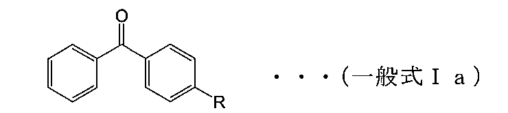
一般式Iaで表される材料は、ベンゾフェノン骨格を含んでいるのでエネルギー線を効率よく吸収し、ベンゾフェノンのカルボニル基のn軌道の電子がπ*軌道に励起され、接触するポリマーのアルキル鎖と反応する。接触するポリマーのアルキル鎖は、第3級炭素が最も反応しやすい。このため、エネルギー線の照射により、一般式Iaで表される材料からなる自己組織化単分子膜2とポリマーを架橋させることができる。
さらに、自己組織化単分子膜2の材料は、一般式Iaで表される材料のうち、合成が簡便で、コストが安いものが好ましい。このような材料として、例えば、下記の一般式Ibで表されるベンゾフェノン骨格を含むシランカップリング剤を用いることができる。
自己組織化単分子膜2を形成する方法としては、スピンコーティング、ディップコーティング、気相成長、ドクターブレード法、カーテンコーティングなどを用いることができる。なお、自己組織化単分子膜2を形成する前に、基板1の表面に付着した有機不純物を除去するために、基板1への紫外線照射などの前処理を行うことが好ましい。
自己組織化単分子膜2の形成にスピンコーティングを用いる場合、自己組織化単分子膜2の材料を溶剤で希釈するかまたは原液のまま基板1上にスピンコートし、必要に応じてホットプレートなどの上でベークして自己組織化単分子膜2を形成する。なお、単分子膜を超えて基板1に吸着されている余分な自己組織化単分子膜2の材料は洗い流される。
スピンコーティングにおいて、自己組織化単分子膜2の材料を溶剤で希釈する濃度は1~30wt%が好ましいが、特に限定されない。基板1に対する塗れ広がりの程度に応じてその濃度を調整することが好ましい。
用いる溶剤は、自己組織化単分子膜2の材料によっても異なるが、自己組織化単分子膜2の材料と反応を起こさないものが好ましい。このような溶剤として、トルエン、キシレン、メシチレンなどの芳香族炭化水素類、シクロヘキサン、シクロヘプタン、シクロオクタン、シクロノナンなどのシクロアルカン類、ヘキサン、ヘプタン、オクタン、ノナン、デカンなどのアルカン類、メタノール、エタノール、1-プロパノール、2-プロパノールなどのアルキルアルコール類などを用いることができる。
上述した溶剤以外にも、反応性、基板1との濡れ性、揮発性の観点から、一般的なフォトレジストの溶剤に用いられるケトン類、セロソルブ類、およびエステル類といった有機溶媒を用いることもできる。ケトン類としては、シクロヘキサノン、アセトン、エチルメチルケトン、メチルイソブチルケトンなどが挙げられる。セロソルブル類としては、メチルセロソルブ、メチルセロソルブアセテート、エチルセロソルブアセテート、ブチルセロソルブアセテートなどが挙げられる。エステル類としては、酢酸エチル、酢酸ブチル、酢酸イソアミル、γ-ブチロラクトン、3-メトキシプロピオン酸メチルが挙げられる。
溶剤は、必要に応じて2種以上を組み合わせて用いることができる。基板1の表面の官能基との反応性の観点から脱水溶剤を用いることが好ましい。
ホットプレートなどの上でベークするときの温度は、自己組織化単分子膜2の材料が基板1の表面の官能基と化学結合するための活性化エネルギーを超えるエネルギーを発生させるため、100~200℃が好ましい。
単分子膜を超えて基板1に吸着されている余分な自己組織化単分子膜2の材料を洗い流す(リンスする)ときに使用する溶剤は、自己組織化単分子膜2の材料を希釈するときに用いた溶剤と同様のものを用いることが好ましい。
自己組織化単分子膜2の形成にディップコーティングを用いる場合、自己組織化単分子膜2の材料を溶剤で希釈し、その希釈溶液中に基板1を一定時間浸漬させて、自己組織化単分子膜2を形成する。
ディップコーティングにおいて、自己組織化単分子膜2の材料を溶剤で希釈する濃度は1~30wt%が好ましい。
用いる溶剤は、スピンコーティングで用いる溶剤と同様に、自己組織化単分子膜2の材料と反応を起こさないものが好ましい。このような溶剤として、トルエン、キシレン、メシチレンなどの芳香族炭化水素類、シクロヘキサン、シクロヘプタン、シクロオクタン、シクロノナンなどのシクロアルカン類、ヘキサン、ヘプタン、オクタン、ノナン、デカンなどのアルカン類、メタノール、エタノール、1-プロパノール、2-プロパノールなどのアルキルアルコール類などを用いることができる。基板1の表面の官能基との反応性の観点から脱水溶剤を用いることが好ましい。
浸漬時間は、濃度、反応性などにも依存するが、1~60分間が好ましい。反応速度の観点から溶液を加熱して基板1を浸漬させてもよい。浸漬温度は、溶剤の沸点以下で、自己組織化単分子膜2の材料が基板1の表面の官能基に反応する前に分解しない温度に設定され、一般的に40~100℃に調節される。
単分子膜を超えて自己組織化単分子膜2に吸着されている余分な自己組織化単分子膜2の材料を洗い流す(リンスする)ときに使用する溶剤は、浸漬に使用した溶剤と同様のものを用いることが好ましい。リンス後に窒素やアルゴンなどの不活性ガスを吹き付けて溶剤を吹き飛ばし、場合によってはホットプレート上で加熱して溶剤を除去することが好ましい。
自己組織化単分子膜2の形成に気相成長を用いる場合、気圧を下げるか温度を上げるかまたはその両方によって自己組織化単分子膜2の材料を気体状態とし、その中へ基板1を導入し、一定時間曝露して基板1の表面に自己組織化単分子膜2を形成する。
気相成長では、自己組織化単分子膜2の材料を気体状態にするために、その材料の蒸気圧特性に応じて、気圧を下げるか温度を上げるかまたはその両方を行う。用いる単分子膜形成材料の沸点に依存するが、材料の安定性の観点から、減圧して気体状態に変わるまで温度を上げることが好ましい。気体状態の自己組織化単分子膜2の材料が存在する空間に基板1を入れるかまたは予め入れておき、1~5時間基板1の表面を曝露することが好ましい。
基板1を曝露した後、必要に応じて、単分子膜を超えて基板1に吸着されている余分な自己組織化単分子膜2の材料を溶剤で洗い流してもよい。この溶剤として、上述したスピンコーティングにおいて用いられる溶剤と同じものを用いることが好ましい。
次に、図1A(b)に示すように、自己組織化単分子膜2上にポリマー膜3を形成する。
ポリマー膜3の材料としては、高エネルギー線の照射により自己組織化単分子膜2と化学結合し、かつその表面上に形成されるポリマーアロイのミクロ相分離構造の配向を整えるために適した表面エネルギーを有するものを用いる。
次に、図1A(c)に示すように、基板1上に高エネルギー線を照射し、ポリマー膜3を自己組織化単分子膜2に化学結合(架橋)させ、ポリマー表面層4を自己組織化単分子膜2上に形成する。なお、ポリマー表面層4を形成した後、ポリマー表面層4上のポリマー膜3の自己組織化単分子膜2に化学結合しなかった部分を除去してもよい。
自己組織化単分子膜2に照射されるエネルギー線は、自己組織化単分子膜2の材料が感度をもつ波長を有するものであれば特に限定されない。具体的には、紫外線、水銀ランプのi線、h線またはg線、キセノンランプ光、新紫外光(たとえばKrFまたはArFなどのエキシマーレーザー光)、X線、シンクロトロンオービタルラジエーション(SR)、電子線、γ線およびイオンビームなどを用いることができる。
次に、図1B(d)に示すように、相分離構造を有するポリマーアロイ5をポリマー表面層4上に形成する。ポリマーアロイ5をポリマー表面層4上に形成することにより、ポリマーアロイ5を自己組織化単分子膜2上に直接形成する場合よりも、ポリマーアロイ5の相分離構造の垂直配向性を高めることができる。
ポリマーアロイ5は、例えば、ブロックコポリマー、異種のホモポリマーをブレンドしたポリマー、ホモポリマーとブロックコポリマーをブレンドしたポリマー、またはグラフトコポリマーである。
ポリマーアロイ5は、第1の相5aおよび第2の相5bからなる相分離構造を有する。ポリマーアロイ5は、例えば、第1の相5aがポリスチレンのブロック鎖からなり、第2の相5bがポリブタジエンのブロック鎖からなるブロックコポリマー、または第1の相5aがポリスチレンのブロック鎖からなり、第2の相5bがポリメチルメタクリレートのブロック鎖からなるブロックコポリマーである。または第1の相5aがポリノルボルナジエンのブロック鎖からなり、第2の相5bがポリメチルメタクリレートのブロック鎖からなるブロックコポリマーである。
また、第1の相5aおよび第2の相5bはラメラ構造を構成することが好ましい。なお、ポリマーアロイ5の相分離構造は、3つ以上の相から構成されてもよい。
ポリマーアロイ5の形成方法は特に限定されない。たとえば、スピンコーティング、ディップコーティング、ドクターブレード法、カーテンコーティング、その他の方法を用いることができる。ポリマーアロイ5の溶液をポリマー表面層4上に塗布した後、必要に応じて、ホットプレート上で加熱して溶剤を除去してもよい。このときの加熱温度は70~120℃が好ましい。
ポリマーアロイ5を相分離させるには、一般的に、ポリマーアロイ5のガラス転移点温度以上の温度でアニールする。例えば、ブロックコポリマーの相分離速度はアニール温度に対して相関性があることが知られている(例えば、A. M. Welander et al., Macromolecules, 41, 2759-2761, 2008参照)。アニール温度が秩序・無秩序転移温度(ODT)を超えて高くなると、無秩序構造になり、相分離構造が得られない。このため、適度な相分離速度が得られる適度な温度でアニールすることが好ましい。ポリマーアロイ5の分子量や種類にもよるが、アニール温度は130~280℃であることが好ましい。アニールはオーブンやホットプレートを用いて行う。オーブンを用いる場合には低温で長時間アニールする。ホットプレートを用いる場合には高温で短時間アニールする。
なお、酸素などの反応性ガスが微量に存在する雰囲気でアニールする場合、アニール温度が高温になるとポリマーアロイ5が分解することがある。そこで、ポリマーアロイ5の分解を防ぐ観点から、アルゴン、窒素などの不活性ガス雰囲気でアニールすることが好ましい。必要に応じて、約3%の水素を含むフォーミングガス雰囲気でアニールしてもよい。
その後、図1B(e)に示すように、ポリマーアロイ5の第1の相5aと第2の相5bのうちのいずれか一方を選択的に除去してもよい。ラメラ構造を構成する第1の相5aと第2の相5bのうちのいずれか一方を選択的に除去することにより、ポリマーアロイ5にラインアンドスペースパターンを形成することができる。なお、ポリマーアロイ5が3つ以上の相から構成される場合は、それらの相のうちの一部の相を除去する。
この工程を行う場合、第1の相5aと第2の相5bは、何らかの方法によりいずれか一方を選択的に除去することのできるブロック鎖からなることが求められる。例えば、ポリスチレンのブロック鎖からなる相とポリブタジエンのブロック鎖からなる相を有するブロックコポリマーにオゾン処理を施すことにより、ポリブタジエンのブロック鎖からなる相を選択的に除去できることが知られている。また、ポリスチレンのブロック鎖からなる相とポリメチルメタクリレートのブロック鎖からなる相を有するブロックコポリマーにO2、CF4などの反応性ガスを用いた反応性イオンエッチング(RIE)を施すことにより、ポリメチルメタクリレートのブロック鎖からなる相を選択的に除去できることが知られている(例えば、K. Asakawa et al., APS March Meeting, 2000を参照)。
そのため、例えば、ポリマーアロイ5が、第1の相5aがポリスチレンのブロック鎖からなり、第2の相5bがポリブタジエンのブロック鎖からなるブロックコポリマーである場合は、オゾン処理により第2の相5bを選択的に除去し、第1の相5aのみを残すことができる。また、ポリマーアロイ5が、第1の相5aがポリスチレンのブロック鎖からなり、第2の相5bがポリメチルメタクリレートのブロック鎖からなるブロックコポリマーである場合や第1の相5aがポリノルボルナジエンのブロック鎖からなり、第2の相5bがポリメチルメタクリレートのブロック鎖からなるブロックコポリマーである場合は、O2、CF4などの反応性ガスを用いたRIEにより第2の相5bを選択的に除去し、第1の相5aのみを残すことができる。
オゾン処理やRIEを施す方法以外に、熱処理またはウェットエッチングを施す方法を用いることができる。主鎖がエネルギー線の照射により切断されるポリマー鎖とエネルギー線に対して難分解性のポリマー鎖とを有するブロックコポリマーをパターン形成材料として用いた場合において、膜に光、もしくは電子線を照射してミクロ相分離構造を構成する1つのポリマー相の主鎖を切断した後、加熱により揮発させるか、ウェットエッチングすることによりそのポリマー相を選択的に除去する。
また、ウェットエッチングを用いる方法では、処理を行う前にエネルギー線を照射しなくても、第1の相5aと第2の相5bの一方を選択的に除去できる現像液を用いると、第1の相5aと第2の相5bの一方を選択的に除去することができる。
現像液は、有機現像液であっても水性現像液(アルカリ現像液)であってもよい。有機現像液としては、メタノール、エタノール、およびイソプロパノールなどのアルコール類、シクロヘキサノン、アセトン、エチルメチルケトン、およびメチルイソブチルケトンなどのケトン類、メチルセロソルブ、メチルセロソルブアセテート、エチルセロソルブアセテート、およびブチルセロソルブアセテートなどセロソルブ類、および酢酸エチル、酢酸ブチル、酢酸イソアミル、γ-ブチロラクトン、および3-メトキシプロピオン酸メチルなどのエステル類といった有機溶媒が挙げられる。上述したような溶剤は、必要に応じて2種以上を組み合わせて用いることができる。
水性現像液としては、有機アルカリ水溶液および無機アルカリ水溶液のいずれを用いてもよい。有機アルカリ水溶液としては、例えばテトラメチルアンモニウムヒドロキシド水溶液、テトラエチルアンモニウムヒドロキシド水溶液、およびコリン水溶液などが挙げられ、無機アルカリ水溶液としては、例えば水酸化カリウム水溶液、および水酸化ナトリウム水溶液などが挙げられる。アルカリ現像液の濃度は限定されない。
また、これらの現像液には、必要に応じて任意の添加剤を添加することもできる。例えば、界面活性剤を添加して現像液の表面張力を下げたり、中性塩を加えて現像を活性にすることもできる。また、現像液の温度も任意であり、冷水を用いることも温水を用いることもできる。
残った第1の相5aは、下地層、すなわち基板1を構成するウエハーや、ウエハー上の金属層または絶縁層、のエッチング用のマスクとして用いることができる。
以下に、本実施の形態の具体例を示す。この具体例においては、基板1としてのシリコンウエハー上に自己組織化単分子膜2としての4-(3’クロロジメチルシリル)プロピルオキシベンゾフェノン(CSBP)の単分子膜を形成し、その上に、ポリマー膜3としてのポリマー膜を形成し、CSBPの単分子膜およびポリマー膜をArFエキシマーレーザーで露光してポリマー表面層4としてのポリマー表面層を形成し、さらにポリマーアロイ5としてのブロックコポリマーのラメラ状のミクロ相分離構造を形成した。
まず、市販の4-ヒドロキシベンゾフェノン(39.6g)と炭酸カリウム(28g)を三口フラスコに入れ、アルゴン置換した。次に、脱水アセトン(120ml)を入れ、よく撹拌してアリルブロミド(18.6ml)を加えた。そして60℃で8時間撹拌した。その後、室温に冷まし、純水(80ml)を加えて攪拌し、ジエチルエーテル(100ml)で2回抽出した。10%NaOH水溶液(100ml)で2回抽出洗浄し、硫酸ナトリウムで乾燥した。エバポレーターにかけ、溶媒を除去して黄白色の残留物を得た。残留物をメタノールから再結晶して吸引ろ過して、真空中で乾燥後、純粋な生成物である4-アリルオキシベンゾフェノン(以下ABPという)を得た(収量43.7g、収率91.9%)。
ABPは、下記の化学式で表される。

次に、得られたABP(2g)と10%Pt-C(10mg)を三口フラスコに入れ、アルゴン置換した。その中へジメチルクロロシラン(20ml)を入れ、撹拌した。40℃で5時間撹拌した。その後、室温まで冷却し、過剰なジメチルクロロシランを真空除去して、残ったオイル状の生成物である4-(3’クロロジメチルシリル)プロピルオキシベンゾフェノン(以下CSBPという)を得た。得られたオイル状の生成物であるCSBPは、使用する際、脱水トルエンに溶かし、触媒をろ過してそのろ液をそのままシリコンウエハーの表面処理溶液として使用した。
CSBPは、下記の化学式で表される。
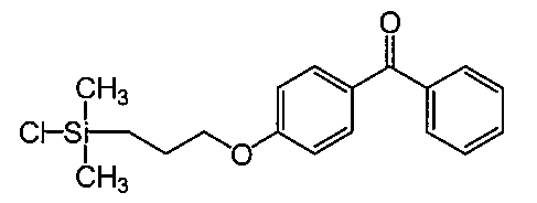
次に、基板1に相当するシリコンウエハー上にCSBPのトルエン溶液(2.26mM、4ml)を垂らし、トリエチルアミンのトルエン溶液(0.247M、2ml)を続けて垂らして、1分間放置し、回転して溶液を振り切った。その後、シクロヘキサノンで全面リンスし、その上にポリマー膜3に相当するポリマー膜用のポリマー溶液を回転塗布した。ポリマー膜用のポリマー溶液は、トルエンに溶かし、回転数2000rpmで塗布した。塗布後に110℃で90秒間ベークして、シリコンウエハー上に自己組織化単分子膜2に相当するCSBPの自己組織化単分子膜を形成し、さらにポリマー膜3に相当するポリマー膜を積層したものを得た。
ポリマー膜用のポリマー溶液は、濃度1wt%に調整した。ポリマー膜用のポリマーとして、Polymer Source社から購入したポリスチレン(PS)とポリメチルメタクリレート(PMMA)のランダム共重合体(PS-r-PMMA)であるP9225-SMMAranを用いた。P9225-SMMAranは、数平均分子量(Mn)が7000、分散度(Mw/Mn)が1.20、PS部分の全体分子量に対する割合(f(PS))が0.59である。
次に、作製したポリマー膜を、ArFエキシマーレーザーにより露光量10~490mJ/cm2で露光した。露光後に、シクロヘキサノンでシリコンウエハー全面をリンスしてポリマー表面層4に相当するポリマー表面層を得た。
別途、ブロックコポリマーの溶液を調製した。ブロックコポリマーとして、Polymer Source社から購入したポリスチレン(PS)とポリメチルメタクリレート(PMMA)のブロック共重合体(PS-b-PMMA)であるP189-SMMAを用いた。P189-SMMAは、PSブロックとPMMAブロックの数平均分子量(Mn)が86500であり、分散度(Mw/Mn)が1.08である。PS部分の全体分子量に対する割合(f(PS))が0.54である。
ブロックコポリマーのポリエチレングリコールモノメチルエーテルアセテート(PGMEA)溶液を2.0wt%の濃度で調整し、ポリマー表面層上に回転数2000rpmで回転塗布し、ホットプレート上において110℃で90秒間ベークしてポリマーアロイ5に相当するブロックコポリマーを形成した。
次いで、窒素雰囲気下のホットプレートベーカー上において220℃で1分間アニール処理することにより、ブロックコポリマーをポリスチレンのブロック鎖からなるPS相とポリメチルメタクリレートのブロック鎖からなるPMMA相に相分離させた。それぞれのサンプル表面の500nm×500nm(500nm□)の領域を、原子間力顕微鏡(Nanoscope II)により、カンチレバーにシリコンチップ[NCH-50]を使用し、タッピングモードで測定して、得られた位相像からラメラ状のミクロ相分離構造の垂直配向性を評価した。
その結果、露光領域全体でバラツキのないラメラ状の垂直配向性を確認でき、観察した領域内において垂直配向性の欠陥がなかった。
さらに、得られた相分離構造を有するブロックコポリマーにO2ガスを用いたRIEを施すことにより、PS相よりもエッチング速度が速いPMMA相を選択的に除去することができた。
また、得られた相分離構造を有するブロックコポリマーをイソプロピルアルコール(IPA)とメチルイソブチルケトン(MIBK)の1:1混合溶液に浸すことにより、PS相よりも溶解速度が速いPMMA相を選択的に除去することができた。
(比較例1)
上記の具体例と同じPSとPMMAのブロックコポリマー(P189-SMMA)の濃度2wt%のポリエチレングリコールモノメチルエーテルアセテート(PGMEA)溶液を作製し、ポリマー表面層を形成せずにシリコンウエハー上に直接回転塗布して、220℃、1分間アニール処理を行なった。しかし、シリコンウエハー上に直接形成したブロックコポリマーには、全くラメラ状の垂直配向性を確認することができなかった。
上記の具体例と同じPSとPMMAのブロックコポリマー(P189-SMMA)の濃度2wt%のポリエチレングリコールモノメチルエーテルアセテート(PGMEA)溶液を作製し、ポリマー表面層を形成せずにシリコンウエハー上に直接回転塗布して、220℃、1分間アニール処理を行なった。しかし、シリコンウエハー上に直接形成したブロックコポリマーには、全くラメラ状の垂直配向性を確認することができなかった。
上記の結果から、本実施の形態のパターン形成方法、形成材料は、ブロックコポリマーに対する高い相分離構造の制御性を有していると考えられる。
〔第2の実施の形態〕
第2の実施の形態は、ポリマー表面層4にパターンを形成した後にポリマーアロイ5を形成する点において第1の実施の形態と異なる。なお、各部材の材料や製造方法等、第1の実施の形態と同様の点については、説明を省略または簡略化する。
第2の実施の形態は、ポリマー表面層4にパターンを形成した後にポリマーアロイ5を形成する点において第1の実施の形態と異なる。なお、各部材の材料や製造方法等、第1の実施の形態と同様の点については、説明を省略または簡略化する。
図2A(a)~(c)、図2B(d)、(e)は、第2の実施の形態に係るポリマーアロイのパターン形成方法を示す斜視図である。
まず、図1A(a)~(c)に示されるポリマー表面層4を形成するまでの工程を第1の実施の形態と同様に行う。
次に、図2A(a)に示すように、ポリマー膜3上にラインアンドスペース等のパターンを有するフォトレジスト6を形成する。
次に、図2A(b)に示すように、フォトレジスト6をマスクとして用いてポリマー表面層4をエッチングし、ポリマー表面層4にフォトレジスト6のパターンを転写する。
次に、図2A(c)に示すように、フォトレジスト6を除去する。
次に、図2B(d)に示すように、相分離構造を有するポリマーアロイ5をポリマー表面層4および露出した自己組織化単分子膜2上に形成する。このとき、ポリマーアロイ5の第1の相5aがポリマー表面層4上に形成され、第2の相5bが露出した自己組織化単分子膜2上に形成される。
例えば、第1の相5aのポリマー表面層4に対する接触角が自己組織化単分子膜2に対する接触角よりも小さく、かつ第2の相5bの自己組織化単分子膜2に対する接触角がポリマー表面層4に対する接触角以下である場合、または、第2の相5bの自己組織化単分子膜2に対する接触角がポリマー表面層4に対する接触角よりも小さく、かつ第1の相5aのポリマー表面層4に対する接触角が自己組織化単分子膜2に対する接触角以下である場合、第1の相5aがポリマー表面層4上に形成され、第2の相5bが露出した自己組織化単分子膜2上に形成される。
その後、図2B(e)に示すように、ポリマーアロイ5の第1の相5aと第2の相5bのうちのいずれか一方を選択的に除去してもよい。なお、ポリマーアロイ5が3つ以上の相から構成される場合は、それらの相のうちの一部の相を除去する。
また、ポリマーアロイ5の第1の相5aと第2の相5bの本来のパターン周期がパターニングされたポリマー表面層4のパターン周期よりも小さい場合は、図3(a)に示すように、ポリマー表面層4の1つのラインおよび自己組織化単分子膜2の1つのスペース上に複数のポリマーアロイ5の相が形成される。この場合、ポリマーアロイ5の相分離構造のパターンの周期を、露光装置の解像度限界によるフォトレジスト6のパターンの最小周期よりも小さくすることができる。
その後、図3(b)に示すように、ポリマーアロイ5の第1の相5aと第2の相5bのうちのいずれか一方を選択的に除去すれば、フォトリソグラフィの露光装置の解像度限界を超える微細なラインアンドスペースパターンを有するマスクを得ることができる。
以下に、本実施の形態の具体例を示す。この具体例においては、基板1としてのシリコンウエハー上に自己組織化単分子膜2としてのCSBPの単分子膜を形成し、その上に、ポリマー膜3としてのポリマー膜を形成し、CSBPの単分子膜およびポリマー膜をArFエキシマーレーザーで露光してポリマー表面層4としてのポリマー表面層を形成し、さらにフォトレジスト6としてのフォトレジストを積層してArFエキシマーレーザーでパターン露光、現像して、そのレジストパターンを通してO2ガスを用いた反応性イオンエッチング(RIE)でポリマー表面層をパターニングして、レジストパターンを剥離後、形成したポリマー表面層のパターン上でポリマーアロイ5としてのブロックコポリマーのラメラ状のミクロ相分離のパターンを形成した。
まず、基板1に相当するシリコンウエハー上にCSBPのトルエン溶液(2.26mM、4ml)を垂らし、トリエチルアミンのトルエン溶液(0.247M、2mL)を続けて垂らして、1分間放置し、回転して溶液を振り切った。その後、シクロヘキサノンで全面リンスし、その上にポリマー膜3に相当するポリマー膜用のポリマー溶液を回転塗布した。ポリマー膜用のポリマー溶液は、トルエンに溶かし、回転数2000rpmで塗布した。塗布後に110℃で90秒間ベークして、シリコンウエハー上に自己組織化単分子膜2に相当するCSBPの自己組織化単分子膜を形成し、さらにポリマー膜3に相当するポリマー膜を積層したものを得た。
ポリマー膜用のポリマーとして、Polymer Source社から購入したポリスチレン(PS)のP1071-St、P8007-S、P8096-Sをそれぞれ用いた。P1071-St、P8007-S、P8096-Sは、数平均分子量(Mn)がそれぞれ、115900、30000、8000、分散度(Mw/Mn)が1.04、1.07、1.06PS部分の全体分子量に対する割合(f(PS))が0.59である。P1071-St、P8007-S、P8096-Sを用いたポリマー溶液の濃度は、いずれも1.0wt%とした。
次に、作製したポリマー膜を、ArFエキシマーレーザーにより露光量490mJ/cm2で露光した。露光後に、シクロヘキサノンでシリコンウエハー全面をリンスしてポリマー表面層4に相当するポリマー表面層を得た。
次いで、作製したポリマー表面層上にフォトレジスト6に相当するフォトレジストを回転塗布した。フォトレジストは、JSR株式会社から購入したAR1687を用いた。そのフォトレジストをArFエキシマーレーザーでパターン露光した。ここで、ハーフピッチ100、95、90、85、80、75、70、65nmのラインアンドスペース(1:1)パターンをそれぞれ転写した。露光量は25.5mJ/cm2で露光した。露光後、多摩化学株式会社から購入した2.38%の水酸化テトラメチルアンモニウム水溶液(AD-10)で現像してハーフピッチ100、95、90、85、80、75、70、65nmのラインアンドスペース(1:1)パターンをそれぞれフォトレジストに形成した。
フォトレジストをパターニングした後、誘導結合型反応性エッチング装置(ICP-RIE)でO2プラズマエッチングを行なった。Coil PowerとPlaten Powerはそれぞれ10、10Wで2分間行い、フォトレジストをマスクとしてポリマー表面層をパターン除去した。その後、シクロヘキサノンで1分間リンスして、フォトレジストを除去して、ハーフピッチ100、95、90、85、80、75、70、65nmのラインアンドスペース(1:1)パターンをそれぞれポリマー表面層に形成した。
別途、ブロックコポリマーの溶液を調製した。ブロックコポリマーとして、Polymer Source社から購入したポリスチレン(PS)とポリメチルメタクリレート(PMMA)のブロック共重合体(PS-b-PMMA)であるP189-SMMAを用いた。P189-SMMAは、PSブロックとPMMAブロックの数平均分子量(Mn)が86500であり、分散度(Mw/Mn)が1.08である。PS部分の全体分子量に対する割合(f(PS))が0.54である。
ブロックコポリマーのポリエチレングリコールモノメチルエーテルアセテート(PGMEA)溶液を2.0wt%の濃度で調整し、ポリマー表面層上に回転数2000rpmで回転塗布し、ホットプレート上において110℃で90秒間ベークしてポリマーアロイ5に相当するブロックコポリマーを形成した。
次いで、窒素雰囲気下でアニール処理することにより、ブロックコポリマーをポリスチレンのブロック鎖からなるPS相とポリメチルメタクリレートのブロック鎖からなるPMMA相に相分離させた。それぞれのサンプル表面の500nm×500nm(500nm□)の領域を、原子間力顕微鏡(Nanoscope III)により、カンチレバーにシリコンチップ[NCH-50]を使用し、タッピングモードで測定して、得られた位相像からラメラ状のミクロドメイン構造のパターン配向性を評価した。
その結果、P1071-St、P8007-S、P8096-Sのいずれのポリマーを用いた場合も、ブロックコポリマーにハーフピッチ25nmのパターン配向したラメラ状のミクロ相分離構造が形成されることが確認された。
また、ハーフピッチ100、95、90、85、80、75、70、65nmのラインアンドスペース(1:1)パターンを有するポリマー表面層上のブロックコポリマーのうち、ハーフピッチ75nmのラインアンドスペースパターンを有するポリマー表面層上に形成されたハーフピッチ25nmのラインアンドスペースパターンを有するブロックコポリマーの垂直配向性が最も高いことが確認された。
さらに、得られた相分離構造を有するブロックコポリマーにO2ガスを用いたRIEを施すことにより、PS相よりもエッチング速度が速いPMMA相を選択的に除去することができた。
また、得られた相分離構造を有するブロックコポリマーをイソプロピルアルコール(IPA)とメチルイソブチルケトン(MIBK)の1:1混合溶液に浸すことにより、PS相よりも溶解速度が速いPMMA相を選択的に除去することができる。
〔第3の実施の形態〕
第3の実施の形態は、ポリマー表面層4のパターン形成方法において第2の実施の形態と異なる。なお、各部材の材料や製造方法等、第1、2の実施の形態と同様の点については、説明を省略または簡略化する。
第3の実施の形態は、ポリマー表面層4のパターン形成方法において第2の実施の形態と異なる。なお、各部材の材料や製造方法等、第1、2の実施の形態と同様の点については、説明を省略または簡略化する。
図4(a)、(b)は、第3の実施の形態に係るポリマーアロイのパターン形成方法を示す斜視図である。
まず、図1A(a)、(b)に示されるポリマー膜3を形成するまでの工程を第1の実施の形態と同様に行う。
次に、図4(a)に示すように、高エネルギー線を用いてポリマー膜3およびその下の自己組織化単分子膜2をパターン露光し、高エネルギー線の照射された領域のポリマー膜3と自己組織化単分子膜2を化学結合(架橋)させ、自己組織化単分子膜2上にポリマー表面層4を形成する。すなわち、高エネルギー線を基板1上の一部の領域(パターン領域)に照射し、その一部の領域のポリマー膜3と自己組織化単分子膜2を選択的に化学結合させてポリマー表面層4を形成する。なお、ポリマー表面層4を形成した後、ポリマー表面層4上のポリマー膜3の自己組織化単分子膜2に化学結合しなかった部分を除去してもよい。
次に、図4(b)に示すように、ポリマー表面層4を残して、ポリマー膜3を選択的に除去する。
その後、ポリマーアロイ5を形成する工程以降の工程を第2の実施の形態と同様に行う。
ポリマーアロイ5の第1の相5aと第2の相5bの本来のパターン周期がパターニングされたポリマー表面層4のパターン周期よりも小さい場合は、図3(a)に示すように、ポリマー表面層4の1つのラインおよび自己組織化単分子膜2の1つのスペース上に複数のポリマーアロイ5の相が形成される。この場合、ポリマーアロイ5の相分離構造のパターンの周期を、ポリマー膜3と自己組織化単分子膜2のパターン露光に用いた高エネルギー線の分解能の限界によるポリマー表面層4のパターンの最小周期よりも小さくすることができる。
その後、図3(b)に示すように、ポリマーアロイ5の第1の相5aと第2の相5bのうちのいずれか一方を選択的に除去すれば、高エネルギー線の分解能の限界を超える微細なラインアンドスペースパターンを有するマスクを得ることができる。
(実施の形態の効果)
第1~3の実施の形態によれば、ポリマーアロイを自己組織化単分子膜上にポリマー表面層を介して形成することにより、配向性の高い相分離構造のパターンを短時間でポリマーアロイに形成することができる。また、相分離構造の一部の相を選択的に除去することにより、ポリマーアロイを微細なパターンを有するエッチングマスクとして用いることができる。
第1~3の実施の形態によれば、ポリマーアロイを自己組織化単分子膜上にポリマー表面層を介して形成することにより、配向性の高い相分離構造のパターンを短時間でポリマーアロイに形成することができる。また、相分離構造の一部の相を選択的に除去することにより、ポリマーアロイを微細なパターンを有するエッチングマスクとして用いることができる。
本発明は、第1~3の実施の形態に限定されず、発明の主旨を逸脱しない範囲内において種々変形実施が可能である。また、第1~3の実施の形態に示されるパターン形成方法の工程順序は、上述したものに限定されない。
1 基板、 2 自己組織化単分子膜、 3 ポリマー膜、 4 ポリマー表面層、 5 ポリマーアロイ、 5a 第1の相、 5b 第2の相、 6 フォトレジスト
Claims (15)
- 基板上に自己組織化単分子膜とポリマー膜を積層し、
エネルギー線を照射することにより前記ポリマー膜と前記自己組織化単分子膜を化学結合させて、ポリマー表面層を前記自己組織化単分子膜上に形成し、
相分離構造のパターンを有するポリマーアロイを前記ポリマー表面層上に形成する、
ことを含むパターン形成方法。 - 前記ポリマー表面層を形成した後、前記ポリマー表面層上の前記ポリマー膜の化学結合しなかった部分を除去することをさらに含む、
請求項1に記載されたパターン形成方法。 - 前記エネルギー線を前記基板上の一部の領域に選択的に照射し、前記一部の領域のポリマー膜と前記自己組織化単分子膜を選択的に化学結合させて前記ポリマー表面層を形成し、
前記エネルギー線が照射されなかった領域の前記ポリマー膜を除去した後に前記ポリマーアロイを形成する、
請求項1に記載されたパターン形成方法。 - 前記ポリマーアロイの前記相分離構造は第1および第2の相により構成され、
前記ポリマー表面層上に前記第1の相が形成され、
前記エネルギー線が照射されなかった領域の前記ポリマー膜が除去されることにより露出した前記自己組織化単分子膜の表面上に前記第2の相が形成される、
請求項3に記載されたパターン形成方法。 - 前記ポリマー表面層上にフォトレジストを塗布し、紫外線または電子線を用いたパターン露光および現像により前記フォトレジストにパターンを形成し、
前記パターンを形成された前記フォトレジストに覆われていない領域の前記ポリマー表面層をエッチングにより除去し、前記パターンを前記ポリマー表面層に転写する工程と、 前記パターンを前記ポリマー表面層に転写した後、前記フォトレジストを溶剤により除去する、
ことをさらに含み、
前記フォトレジストを除去した後に前記ポリマーアロイを形成する、請求項1に記載されたパターン形成方法。 - 前記ポリマーアロイの前記相分離構造は第1および第2の相により構成され、
前記ポリマー表面層上に前記第1の相が形成され、
前記フォトレジストに覆われていない前記領域の前記ポリマー表面層が除去されることにより露出した前記自己組織化単分子膜の表面上に前記第2の相が形成される、
請求項5に記載されたパターン形成方法。 - 前記相分離構造の一部の相を選択的に除去することをさらに含む、
請求項1に記載されたパターン形成方法。 - 前記一部の相は前記相分離構造の他の相よりもエッチング耐性の低いブロック鎖からなる相であり、反応性化学エッチングにより除去される、
請求項7に記載されたパターン形成方法。 - 前記一部の相は前記相分離構造の他の相よりも現像液に溶解しやすいブロック鎖からなる相であり、現像液を用いて除去される、
請求項7に記載されたパターン形成方法。 - 前記ポリマーアロイは、ブロックコポリマー、グラフトコポリマー、ブレンドポリマーの中の少なくとも1種から構成される、
請求項1に記載されたパターン形成方法。 - 前記ポリマーアロイは、
芳香族骨格、アクリル骨格、および脂環式骨格を有するブロックコポリマー、
芳香族骨格を有するホモポリマー、アクリル骨格を有するホモポリマー、および脂環式骨格を有するホモポリマーの中の少なくとも2つを含むブレンドポリマー、
もしくは芳香族骨格を有するホモポリマー、アクリル骨格を有するホモポリマー、または脂環式骨格を有するホモポリマーと前記ブロックコポリマーとを含むポリマーである、請求項1に記載されたパターン形成方法。 - 前記自己組織化単分子膜は、光重合開始剤の誘導体からなる、
請求項1に記載されたパターン形成方法。 - 前記自己組織化単分子膜は、下記の一般式1(一般式1中のR1は、アルキルシリル基、シリル基、アルキルハロゲン化シリル基、ハロゲン化シリル基、アルキルチオール基、チオール基、アルキルヒドロキシ基、ヒドロキシ基、アルキルカルボキシル基、またはカルボキシル基であり、アルキル鎖の中に酸素やハロゲンなどを有してもよい)で表される、ベンゾフェノンを構成要素に含む化合物からなる、
請求項12に記載されたパターン形成方法。

- エネルギー線の照射により自己組織化単分子膜と化学結合する性質を有し、もしくは、エネルギー線の照射によりベンゾフェノンと架橋反応する性質を有し、さらに相分離構造を有するポリマーアロイ形成の下地として用いられるポリマーアロイ下地材料。
- 前記ポリマーアロイは、ブロックコポリマー、グラフトコポリマー、ブレンドポリマーの中の少なくとも1種から構成される、
請求項14に記載されたポリマーアロイ下地材料。
Priority Applications (3)
| Application Number | Priority Date | Filing Date | Title |
|---|---|---|---|
| KR1020137001360A KR101372152B1 (ko) | 2010-07-28 | 2011-07-15 | 패턴 형성 방법 및 중합체 알로이 기재 |
| CN201180035598.2A CN103003918B (zh) | 2010-07-28 | 2011-07-15 | 图案形成方法和聚合物合金基材 |
| US13/750,007 US8986488B2 (en) | 2010-07-28 | 2013-01-25 | Pattern formation method and polymer alloy base material |
Applications Claiming Priority (2)
| Application Number | Priority Date | Filing Date | Title |
|---|---|---|---|
| JP2010-169279 | 2010-07-28 | ||
| JP2010169279A JP5300799B2 (ja) | 2010-07-28 | 2010-07-28 | パターン形成方法及びポリマーアロイ下地材料 |
Related Child Applications (1)
| Application Number | Title | Priority Date | Filing Date |
|---|---|---|---|
| US13/750,007 Continuation US8986488B2 (en) | 2010-07-28 | 2013-01-25 | Pattern formation method and polymer alloy base material |
Publications (1)
| Publication Number | Publication Date |
|---|---|
| WO2012014700A1 true WO2012014700A1 (ja) | 2012-02-02 |
Family
ID=45529916
Family Applications (1)
| Application Number | Title | Priority Date | Filing Date |
|---|---|---|---|
| PCT/JP2011/066222 Ceased WO2012014700A1 (ja) | 2010-07-28 | 2011-07-15 | パターン形成方法及びポリマーアロイ下地材料 |
Country Status (6)
| Country | Link |
|---|---|
| US (1) | US8986488B2 (ja) |
| JP (1) | JP5300799B2 (ja) |
| KR (1) | KR101372152B1 (ja) |
| CN (1) | CN103003918B (ja) |
| TW (1) | TWI482201B (ja) |
| WO (1) | WO2012014700A1 (ja) |
Cited By (4)
| Publication number | Priority date | Publication date | Assignee | Title |
|---|---|---|---|---|
| US8575587B2 (en) | 2011-03-07 | 2013-11-05 | Kabushiki Kaisha Toshiba | Storage device and method of manufacturing the same |
| US8673771B2 (en) | 2012-03-01 | 2014-03-18 | Kabushiki Kaisha Toshiba | Pattern forming method |
| WO2014046241A1 (ja) * | 2012-09-21 | 2014-03-27 | 東京エレクトロン株式会社 | 基板処理システム |
| WO2014119444A1 (ja) * | 2013-01-30 | 2014-08-07 | 東京エレクトロン株式会社 | 基板処理方法及びコンピュータ記憶媒体 |
Families Citing this family (43)
| Publication number | Priority date | Publication date | Assignee | Title |
|---|---|---|---|---|
| JP5542766B2 (ja) * | 2011-09-26 | 2014-07-09 | 株式会社東芝 | パターン形成方法 |
| JP2013201356A (ja) * | 2012-03-26 | 2013-10-03 | Toshiba Corp | 露光方法及びパターン形成方法 |
| JP6177958B2 (ja) * | 2012-04-06 | 2017-08-09 | 東京エレクトロン株式会社 | パターン形成方法、パターン形成装置、及びコンピュータ可読記憶媒体 |
| JP5918122B2 (ja) | 2012-04-06 | 2016-05-18 | 東京エレクトロン株式会社 | パターン形成方法、パターン形成装置、及びコンピュータ可読記憶媒体 |
| JP5758846B2 (ja) * | 2012-05-23 | 2015-08-05 | 東京エレクトロン株式会社 | パターン形成方法、パターン形成装置、及びコンピュータ可読記憶媒体 |
| JP6020991B2 (ja) * | 2012-06-28 | 2016-11-02 | 国立研究開発法人理化学研究所 | 微細パターン形成方法、現像液 |
| JP5902573B2 (ja) | 2012-07-18 | 2016-04-13 | 株式会社東芝 | パターン形成方法 |
| JP6239813B2 (ja) | 2012-07-18 | 2017-11-29 | 株式会社Screenセミコンダクターソリューションズ | 基板処理装置および基板処理方法 |
| JP5764102B2 (ja) * | 2012-09-05 | 2015-08-12 | 株式会社東芝 | パターン形成方法 |
| JP5758363B2 (ja) * | 2012-09-07 | 2015-08-05 | 株式会社東芝 | パターン形成方法 |
| JP5752655B2 (ja) * | 2012-09-10 | 2015-07-22 | 株式会社東芝 | パターン形成方法 |
| JP5813604B2 (ja) * | 2012-09-21 | 2015-11-17 | 株式会社東芝 | パターン形成方法 |
| EP2717296B1 (en) * | 2012-10-02 | 2016-08-31 | Imec | Etching of block-copolymers |
| JP5823424B2 (ja) * | 2013-02-15 | 2015-11-25 | 東京エレクトロン株式会社 | 基板処理方法、プログラム、コンピュータ記憶媒体及び基板処理システム |
| JP6467121B2 (ja) * | 2013-02-20 | 2019-02-06 | 東京応化工業株式会社 | 相分離構造を含む構造体の製造方法 |
| JP5768074B2 (ja) * | 2013-02-28 | 2015-08-26 | 株式会社東芝 | パターン形成方法 |
| JP5802233B2 (ja) * | 2013-03-27 | 2015-10-28 | 株式会社東芝 | パターン形成方法 |
| JP5981392B2 (ja) | 2013-06-19 | 2016-08-31 | 株式会社東芝 | パターン形成方法 |
| US9382444B2 (en) * | 2013-06-24 | 2016-07-05 | Dow Global Technologies Llc | Neutral layer polymers, methods of manufacture thereof and articles comprising the same |
| JP2015028967A (ja) * | 2013-07-30 | 2015-02-12 | 株式会社東芝 | 半導体発光素子及び発光装置 |
| KR102107227B1 (ko) | 2013-12-02 | 2020-05-07 | 에스케이하이닉스 주식회사 | 블록 코폴리머를 이용한 패턴 형성을 위한 구조, 패턴 형성 방법, 및 이를 이용한 반도체소자 제조방법 |
| KR101674972B1 (ko) * | 2013-12-26 | 2016-11-10 | 한국과학기술원 | 나노 스케일 패터닝 방법 및 이로부터 제조된 전자기기용 집적소자 |
| KR102160791B1 (ko) * | 2014-02-03 | 2020-09-29 | 삼성디스플레이 주식회사 | 블록 공중합체 및 이를 사용한 패턴 형성 방법 |
| KR20150101875A (ko) | 2014-02-27 | 2015-09-04 | 삼성전자주식회사 | 블록 공중합체를 이용한 미세 패턴 형성 방법 |
| WO2015170724A1 (ja) * | 2014-05-08 | 2015-11-12 | 国立研究開発法人科学技術振興機構 | ポリマーブラシ |
| JP2016054214A (ja) * | 2014-09-03 | 2016-04-14 | 株式会社東芝 | パターン形成方法 |
| US9396958B2 (en) * | 2014-10-14 | 2016-07-19 | Tokyo Electron Limited | Self-aligned patterning using directed self-assembly of block copolymers |
| JP2016111115A (ja) * | 2014-12-04 | 2016-06-20 | 東京エレクトロン株式会社 | 基板処理方法、プログラム、コンピュータ記憶媒体及び基板処理システム |
| US20170345643A1 (en) * | 2014-12-24 | 2017-11-30 | Intel Corporation | Photodefinable alignment layer for chemical assisted patterning |
| FR3031749B1 (fr) * | 2015-01-21 | 2018-09-28 | Arkema France | Procede d'amelioration de l'uniformite de dimension critique de films ordonnes de copolymeres a blocs |
| KR101932799B1 (ko) | 2015-02-17 | 2018-12-26 | 주식회사 엘지화학 | 블록 공중합체 자기 조립 패턴의 습식 식각 방법 |
| WO2018043305A1 (ja) * | 2016-09-01 | 2018-03-08 | Jsr株式会社 | 基材表面の選択的修飾方法及び組成物 |
| JP6811638B2 (ja) | 2017-02-14 | 2021-01-13 | 株式会社Screenホールディングス | 基板処理方法及びその装置 |
| KR102498632B1 (ko) * | 2018-08-16 | 2023-02-10 | 주식회사 엘지화학 | 기판의 제조 방법 |
| JP7365898B2 (ja) * | 2019-12-27 | 2023-10-20 | 東京エレクトロン株式会社 | 成膜方法及び成膜装置 |
| KR102488382B1 (ko) * | 2021-04-19 | 2023-01-17 | 한국화학연구원 | 클릭반응을 이용한 고밀도 및 고안정성 cnt 필름 코팅 기판 및 이의 제조방법 |
| KR102477148B1 (ko) * | 2021-09-06 | 2022-12-13 | 한국화학연구원 | 클릭반응을 이용한 cnt 트랜지스터 및 이의 제조방법 |
| JP2023045109A (ja) * | 2021-09-21 | 2023-04-03 | キオクシア株式会社 | 組成物、パターン形成方法及び半導体装置 |
| KR102488388B1 (ko) * | 2022-03-30 | 2023-01-13 | 한국화학연구원 | 클릭반응을 이용한 패턴화된 cnt 필름 코팅 기판 및 이의 제조방법 |
| US12290835B2 (en) | 2022-07-18 | 2025-05-06 | Tokyo Electron Limited | Methods for stabilization of self-assembled monolayers (SAMs) using sequentially pulsed initiated chemical vapor deposition (spiCVD) |
| US11691175B1 (en) | 2022-07-18 | 2023-07-04 | Tokyo Electron Limited | Methods for area-selective deposition of polymer films using sequentially pulsed initiated chemical vapor deposition (spiCVD) |
| JP2024064500A (ja) * | 2022-10-28 | 2024-05-14 | 東京エレクトロン株式会社 | 成膜方法および成膜装置 |
| US12604685B2 (en) | 2023-07-19 | 2026-04-14 | Tokyo Electron Limited | Methods for controlling spin-on self-assembled monolayer (SAM) selectivity |
Citations (4)
| Publication number | Priority date | Publication date | Assignee | Title |
|---|---|---|---|---|
| JP2006093644A (ja) * | 2004-08-25 | 2006-04-06 | Seiko Epson Corp | 微細構造体の製造方法、露光装置、電子機器 |
| WO2007127496A2 (en) * | 2006-03-23 | 2007-11-08 | Micron Technology, Inc. | Topography directed patterning |
| WO2010055601A1 (ja) * | 2008-11-12 | 2010-05-20 | パナソニック株式会社 | ブロックコポリマーの自己組織化促進方法及びそれを用いたブロックコポリマーの自己組織化パターン形成方法 |
| JP2011129874A (ja) * | 2009-11-19 | 2011-06-30 | Toshiba Corp | パターン形成方法及びパターン形成装置 |
Family Cites Families (25)
| Publication number | Priority date | Publication date | Assignee | Title |
|---|---|---|---|---|
| JPH0432104A (ja) | 1990-05-25 | 1992-02-04 | Fuji Photo Film Co Ltd | 新規導電性高分子及びそれを用いた導電性材料 |
| JP3940546B2 (ja) * | 1999-06-07 | 2007-07-04 | 株式会社東芝 | パターン形成方法およびパターン形成材料 |
| JP3576056B2 (ja) | 1999-12-28 | 2004-10-13 | 株式会社東芝 | 記録媒体の製造方法および記録媒体 |
| JP3793040B2 (ja) | 2001-05-09 | 2006-07-05 | 株式会社東芝 | 記録媒体およびその製造方法 |
| KR100473799B1 (ko) | 2001-09-12 | 2005-03-07 | 학교법인 포항공과대학교 | 나노미터 수준의 고정밀 패턴 형성방법 |
| US6746825B2 (en) * | 2001-10-05 | 2004-06-08 | Wisconsin Alumni Research Foundation | Guided self-assembly of block copolymer films on interferometrically nanopatterned substrates |
| JP3967114B2 (ja) | 2001-11-22 | 2007-08-29 | 株式会社東芝 | 加工方法 |
| US7252862B2 (en) * | 2004-08-30 | 2007-08-07 | Hewlett-Packard Development Company, L.P. | Increasing adhesion in an imprinting procedure |
| JP5414011B2 (ja) * | 2006-05-23 | 2014-02-12 | 国立大学法人京都大学 | 微細構造体、パターン媒体、及びそれらの製造方法 |
| JP5132117B2 (ja) | 2006-10-10 | 2013-01-30 | キヤノン株式会社 | パターン形成方法 |
| US7553760B2 (en) * | 2006-10-19 | 2009-06-30 | International Business Machines Corporation | Sub-lithographic nano interconnect structures, and method for forming same |
| US7604916B2 (en) | 2006-11-06 | 2009-10-20 | 3M Innovative Properties Company | Donor films with pattern-directing layers |
| US8394483B2 (en) * | 2007-01-24 | 2013-03-12 | Micron Technology, Inc. | Two-dimensional arrays of holes with sub-lithographic diameters formed by block copolymer self-assembly |
| JP4649599B2 (ja) * | 2007-05-31 | 2011-03-09 | 独立行政法人産業技術総合研究所 | In2O3薄膜パターン、In(OH)3薄膜パターン及びそれらの作製方法 |
| JP5301872B2 (ja) | 2007-08-29 | 2013-09-25 | 国立大学法人東北大学 | チオール基含有感紫外線化合物および、その用途 |
| KR101355167B1 (ko) * | 2007-12-14 | 2014-01-28 | 삼성전자주식회사 | 적어도 세 개의 고분자 블록을 구비하는 블록 공중합체를이용한 미세 패턴 형성 방법 |
| US7763319B2 (en) * | 2008-01-11 | 2010-07-27 | International Business Machines Corporation | Method of controlling orientation of domains in block copolymer films |
| US7989026B2 (en) | 2008-01-12 | 2011-08-02 | International Business Machines Corporation | Method of use of epoxy-containing cycloaliphatic acrylic polymers as orientation control layers for block copolymer thin films |
| KR20090083091A (ko) * | 2008-01-29 | 2009-08-03 | 삼성전자주식회사 | 블록 공중합체를 이용한 미세 패턴 형성 방법 |
| KR20090087353A (ko) * | 2008-02-12 | 2009-08-17 | 포항공과대학교 산학협력단 | 자기조립 블록 공중합체를 이용한 나노 구조물 제조방법 |
| US8101261B2 (en) * | 2008-02-13 | 2012-01-24 | Micron Technology, Inc. | One-dimensional arrays of block copolymer cylinders and applications thereof |
| JP2010058314A (ja) | 2008-09-02 | 2010-03-18 | Fujifilm Corp | 可撓性基板上ミクロ相分離構造体、およびその製造方法 |
| KR101148208B1 (ko) * | 2008-12-12 | 2012-05-25 | 삼성전자주식회사 | 패턴화된 구조를 가지는 블록공중합체의 나노구조체 및 그 제조방법 |
| US8486613B2 (en) * | 2008-12-12 | 2013-07-16 | Samsung Electronics Co., Ltd. | Method of manufacturing nano-structure and method of manufacturing a pattern using the method |
| WO2011036816A1 (ja) | 2009-09-28 | 2011-03-31 | 株式会社 東芝 | パターン形成方法 |
-
2010
- 2010-07-28 JP JP2010169279A patent/JP5300799B2/ja not_active Expired - Fee Related
-
2011
- 2011-07-15 KR KR1020137001360A patent/KR101372152B1/ko not_active Expired - Fee Related
- 2011-07-15 CN CN201180035598.2A patent/CN103003918B/zh not_active Expired - Fee Related
- 2011-07-15 WO PCT/JP2011/066222 patent/WO2012014700A1/ja not_active Ceased
- 2011-07-27 TW TW100126670A patent/TWI482201B/zh not_active IP Right Cessation
-
2013
- 2013-01-25 US US13/750,007 patent/US8986488B2/en active Active
Patent Citations (4)
| Publication number | Priority date | Publication date | Assignee | Title |
|---|---|---|---|---|
| JP2006093644A (ja) * | 2004-08-25 | 2006-04-06 | Seiko Epson Corp | 微細構造体の製造方法、露光装置、電子機器 |
| WO2007127496A2 (en) * | 2006-03-23 | 2007-11-08 | Micron Technology, Inc. | Topography directed patterning |
| WO2010055601A1 (ja) * | 2008-11-12 | 2010-05-20 | パナソニック株式会社 | ブロックコポリマーの自己組織化促進方法及びそれを用いたブロックコポリマーの自己組織化パターン形成方法 |
| JP2011129874A (ja) * | 2009-11-19 | 2011-06-30 | Toshiba Corp | パターン形成方法及びパターン形成装置 |
Cited By (8)
| Publication number | Priority date | Publication date | Assignee | Title |
|---|---|---|---|---|
| US8575587B2 (en) | 2011-03-07 | 2013-11-05 | Kabushiki Kaisha Toshiba | Storage device and method of manufacturing the same |
| US8673771B2 (en) | 2012-03-01 | 2014-03-18 | Kabushiki Kaisha Toshiba | Pattern forming method |
| WO2014046241A1 (ja) * | 2012-09-21 | 2014-03-27 | 東京エレクトロン株式会社 | 基板処理システム |
| JP2014063908A (ja) * | 2012-09-21 | 2014-04-10 | Tokyo Electron Ltd | 基板処理システム |
| WO2014119444A1 (ja) * | 2013-01-30 | 2014-08-07 | 東京エレクトロン株式会社 | 基板処理方法及びコンピュータ記憶媒体 |
| JP2014146740A (ja) * | 2013-01-30 | 2014-08-14 | Tokyo Electron Ltd | 基板処理方法、プログラム及びコンピュータ記憶媒体 |
| KR20150114476A (ko) * | 2013-01-30 | 2015-10-12 | 도쿄엘렉트론가부시키가이샤 | 기판 처리 방법 및 컴퓨터 기억 매체 |
| KR102122343B1 (ko) | 2013-01-30 | 2020-06-12 | 도쿄엘렉트론가부시키가이샤 | 기판 처리 방법 및 컴퓨터 기억 매체 |
Also Published As
| Publication number | Publication date |
|---|---|
| TWI482201B (zh) | 2015-04-21 |
| US8986488B2 (en) | 2015-03-24 |
| TW201214514A (en) | 2012-04-01 |
| JP5300799B2 (ja) | 2013-09-25 |
| CN103003918A (zh) | 2013-03-27 |
| US20130133825A1 (en) | 2013-05-30 |
| KR101372152B1 (ko) | 2014-03-07 |
| CN103003918B (zh) | 2015-08-12 |
| JP2012033534A (ja) | 2012-02-16 |
| KR20130054982A (ko) | 2013-05-27 |
Similar Documents
| Publication | Publication Date | Title |
|---|---|---|
| JP5300799B2 (ja) | パターン形成方法及びポリマーアロイ下地材料 | |
| JP5694109B2 (ja) | パターン形成方法 | |
| JP5254381B2 (ja) | パターン形成方法 | |
| JP5318217B2 (ja) | パターン形成方法 | |
| US8623458B2 (en) | Methods of directed self-assembly, and layered structures formed therefrom | |
| US8828493B2 (en) | Methods of directed self-assembly and layered structures formed therefrom | |
| JP6316788B2 (ja) | レリーフ画像形成方法 | |
| TWI387998B (zh) | 微影方法 | |
| CN108137313B (zh) | 用于嵌段共聚物自组装的组合物和方法 | |
| JP2010115832A (ja) | ブロックコポリマーの自己組織化促進方法及びそれを用いたブロックコポリマーの自己組織化パターン形成方法 | |
| EP3500637B1 (en) | Polymer compositions for self-assembly applications | |
| US9891522B2 (en) | Method and composition of a chemically amplified copolymer resist | |
| CN102540710B (zh) | 抗蚀图改善材料、抗蚀图形成方法和半导体装置制造方法 |
Legal Events
| Date | Code | Title | Description |
|---|---|---|---|
| 121 | Ep: the epo has been informed by wipo that ep was designated in this application |
Ref document number: 11812292 Country of ref document: EP Kind code of ref document: A1 |
|
| ENP | Entry into the national phase |
Ref document number: 20137001360 Country of ref document: KR Kind code of ref document: A |
|
| NENP | Non-entry into the national phase |
Ref country code: DE |
|
| 122 | Ep: pct application non-entry in european phase |
Ref document number: 11812292 Country of ref document: EP Kind code of ref document: A1 |