WO2011021607A1 - プラズマ処理装置および基板処理方法 - Google Patents
プラズマ処理装置および基板処理方法 Download PDFInfo
- Publication number
- WO2011021607A1 WO2011021607A1 PCT/JP2010/063831 JP2010063831W WO2011021607A1 WO 2011021607 A1 WO2011021607 A1 WO 2011021607A1 JP 2010063831 W JP2010063831 W JP 2010063831W WO 2011021607 A1 WO2011021607 A1 WO 2011021607A1
- Authority
- WO
- WIPO (PCT)
- Prior art keywords
- inner conductor
- plasma processing
- plate
- stub
- microwave
- Prior art date
- Legal status (The legal status is an assumption and is not a legal conclusion. Google has not performed a legal analysis and makes no representation as to the accuracy of the status listed.)
- Ceased
Links
Images








Classifications
-
- H—ELECTRICITY
- H01—ELECTRIC ELEMENTS
- H01J—ELECTRIC DISCHARGE TUBES OR DISCHARGE LAMPS
- H01J37/00—Discharge tubes with provision for introducing objects or material to be exposed to the discharge, e.g. for the purpose of examination or processing thereof
- H01J37/32—Gas-filled discharge tubes
- H01J37/32009—Arrangements for generation of plasma specially adapted for examination or treatment of objects, e.g. plasma sources
- H01J37/32192—Microwave generated discharge
-
- C—CHEMISTRY; METALLURGY
- C23—COATING METALLIC MATERIAL; COATING MATERIAL WITH METALLIC MATERIAL; CHEMICAL SURFACE TREATMENT; DIFFUSION TREATMENT OF METALLIC MATERIAL; COATING BY VACUUM EVAPORATION, BY SPUTTERING, BY ION IMPLANTATION OR BY CHEMICAL VAPOUR DEPOSITION, IN GENERAL; INHIBITING CORROSION OF METALLIC MATERIAL OR INCRUSTATION IN GENERAL
- C23C—COATING METALLIC MATERIAL; COATING MATERIAL WITH METALLIC MATERIAL; SURFACE TREATMENT OF METALLIC MATERIAL BY DIFFUSION INTO THE SURFACE, BY CHEMICAL CONVERSION OR SUBSTITUTION; COATING BY VACUUM EVAPORATION, BY SPUTTERING, BY ION IMPLANTATION OR BY CHEMICAL VAPOUR DEPOSITION, IN GENERAL
- C23C16/00—Chemical coating by decomposition of gaseous compounds, without leaving reaction products of surface material in the coating, i.e. chemical vapour deposition [CVD] processes
- C23C16/44—Chemical coating by decomposition of gaseous compounds, without leaving reaction products of surface material in the coating, i.e. chemical vapour deposition [CVD] processes characterised by the method of coating
- C23C16/455—Chemical coating by decomposition of gaseous compounds, without leaving reaction products of surface material in the coating, i.e. chemical vapour deposition [CVD] processes characterised by the method of coating characterised by the method used for introducing gases into reaction chamber or for modifying gas flows in reaction chamber
-
- C—CHEMISTRY; METALLURGY
- C23—COATING METALLIC MATERIAL; COATING MATERIAL WITH METALLIC MATERIAL; CHEMICAL SURFACE TREATMENT; DIFFUSION TREATMENT OF METALLIC MATERIAL; COATING BY VACUUM EVAPORATION, BY SPUTTERING, BY ION IMPLANTATION OR BY CHEMICAL VAPOUR DEPOSITION, IN GENERAL; INHIBITING CORROSION OF METALLIC MATERIAL OR INCRUSTATION IN GENERAL
- C23C—COATING METALLIC MATERIAL; COATING MATERIAL WITH METALLIC MATERIAL; SURFACE TREATMENT OF METALLIC MATERIAL BY DIFFUSION INTO THE SURFACE, BY CHEMICAL CONVERSION OR SUBSTITUTION; COATING BY VACUUM EVAPORATION, BY SPUTTERING, BY ION IMPLANTATION OR BY CHEMICAL VAPOUR DEPOSITION, IN GENERAL
- C23C16/00—Chemical coating by decomposition of gaseous compounds, without leaving reaction products of surface material in the coating, i.e. chemical vapour deposition [CVD] processes
- C23C16/44—Chemical coating by decomposition of gaseous compounds, without leaving reaction products of surface material in the coating, i.e. chemical vapour deposition [CVD] processes characterised by the method of coating
- C23C16/50—Chemical coating by decomposition of gaseous compounds, without leaving reaction products of surface material in the coating, i.e. chemical vapour deposition [CVD] processes characterised by the method of coating using electric discharges
- C23C16/511—Chemical coating by decomposition of gaseous compounds, without leaving reaction products of surface material in the coating, i.e. chemical vapour deposition [CVD] processes characterised by the method of coating using electric discharges using microwave discharges
-
- H—ELECTRICITY
- H01—ELECTRIC ELEMENTS
- H01J—ELECTRIC DISCHARGE TUBES OR DISCHARGE LAMPS
- H01J37/00—Discharge tubes with provision for introducing objects or material to be exposed to the discharge, e.g. for the purpose of examination or processing thereof
- H01J37/32—Gas-filled discharge tubes
- H01J37/32009—Arrangements for generation of plasma specially adapted for examination or treatment of objects, e.g. plasma sources
- H01J37/32192—Microwave generated discharge
- H01J37/32211—Means for coupling power to the plasma
- H01J37/3222—Antennas
-
- H—ELECTRICITY
- H01—ELECTRIC ELEMENTS
- H01J—ELECTRIC DISCHARGE TUBES OR DISCHARGE LAMPS
- H01J37/00—Discharge tubes with provision for introducing objects or material to be exposed to the discharge, e.g. for the purpose of examination or processing thereof
- H01J37/32—Gas-filled discharge tubes
- H01J37/32009—Arrangements for generation of plasma specially adapted for examination or treatment of objects, e.g. plasma sources
- H01J37/32192—Microwave generated discharge
- H01J37/32211—Means for coupling power to the plasma
- H01J37/32229—Waveguides
-
- H—ELECTRICITY
- H01—ELECTRIC ELEMENTS
- H01J—ELECTRIC DISCHARGE TUBES OR DISCHARGE LAMPS
- H01J37/00—Discharge tubes with provision for introducing objects or material to be exposed to the discharge, e.g. for the purpose of examination or processing thereof
- H01J37/32—Gas-filled discharge tubes
- H01J37/32431—Constructional details of the reactor
- H01J37/3244—Gas supply means
-
- H—ELECTRICITY
- H05—ELECTRIC TECHNIQUES NOT OTHERWISE PROVIDED FOR
- H05H—PLASMA TECHNIQUE; PRODUCTION OF ACCELERATED ELECTRICALLY-CHARGED PARTICLES OR OF NEUTRONS; PRODUCTION OR ACCELERATION OF NEUTRAL MOLECULAR OR ATOMIC BEAMS
- H05H1/00—Generating plasma; Handling plasma
- H05H1/24—Generating plasma
- H05H1/46—Generating plasma using applied electromagnetic fields, e.g. high frequency or microwave energy
-
- H—ELECTRICITY
- H05—ELECTRIC TECHNIQUES NOT OTHERWISE PROVIDED FOR
- H05H—PLASMA TECHNIQUE; PRODUCTION OF ACCELERATED ELECTRICALLY-CHARGED PARTICLES OR OF NEUTRONS; PRODUCTION OR ACCELERATION OF NEUTRAL MOLECULAR OR ATOMIC BEAMS
- H05H1/00—Generating plasma; Handling plasma
- H05H1/24—Generating plasma
- H05H1/46—Generating plasma using applied electromagnetic fields, e.g. high frequency or microwave energy
- H05H1/461—Microwave discharges
- H05H1/4622—Microwave discharges using waveguides
-
- H—ELECTRICITY
- H05—ELECTRIC TECHNIQUES NOT OTHERWISE PROVIDED FOR
- H05H—PLASMA TECHNIQUE; PRODUCTION OF ACCELERATED ELECTRICALLY-CHARGED PARTICLES OR OF NEUTRONS; PRODUCTION OR ACCELERATION OF NEUTRAL MOLECULAR OR ATOMIC BEAMS
- H05H1/00—Generating plasma; Handling plasma
- H05H1/24—Generating plasma
- H05H1/46—Generating plasma using applied electromagnetic fields, e.g. high frequency or microwave energy
- H05H1/461—Microwave discharges
- H05H1/463—Microwave discharges using antennas or applicators
Definitions
- the present invention relates to a plasma processing apparatus and a substrate processing method, and more particularly to a plasma processing apparatus using a microwave as a plasma source and a substrate processing method performed using such a plasma processing apparatus.
- Semiconductor devices such as LSI (Large Scale Integrated Circuit) are manufactured by subjecting a semiconductor substrate to processing such as etching, CVD (Chemical Vapor Deposition), and sputtering.
- processing such as etching, CVD, and sputtering, there are processing methods using plasma as an energy supply source, that is, plasma etching, plasma CVD, plasma sputtering, and the like.
- Patent Document 1 a technique related to a microwave plasma processing apparatus that uses a microwave when generating plasma is disclosed in Japanese Patent Application Laid-Open No. 2006-179477 (Patent Document 1).
- a dummy load is connected to a cylindrical waveguide between a circular rectangular waveguide and a circular polarization converter.
- the axis of this dummy load is configured to be separated from the reflector toward the circular polarization converter by a quarter wavelength L of the in-tube wavelength of the standing wave reflected by the microwave reflector. Yes.
- the microwave reflected from the radial waveguide box is effectively absorbed by the dummy load.
- FIG. 15 is an enlarged schematic sectional view showing a part of a conventional general plasma processing apparatus.
- the vertical direction of the paper is the vertical direction of the apparatus.
- a microwave is illustrated as an image at a predetermined location.
- a plasma processing apparatus 101 includes a processing container that performs plasma processing on a substrate to be processed therein, a disk-shaped dielectric plate 102 that transmits microwaves into the processing container, and a thin disk.
- a plurality of slot holes penetrating in the plate thickness direction and disposed above the dielectric plate 102 to radiate microwaves to the dielectric plate 102 103, a disk-shaped slow wave plate 104 disposed above the slot antenna plate 103 and propagating microwaves in the radial direction, and a microwave generator 105 disposed outside the processing vessel and generating microwaves
- a microwave supply means 106 for supplying the microwave generated by the microwave generator 105 into the processing container.
- the microwave supply means 106 is provided so as to extend in the vertical direction, and includes a coaxial waveguide 107 connected to the slot antenna plate 103.
- the coaxial waveguide 107 includes a round bar-shaped inner conductor 108 and a cylindrical outer conductor 109 provided on the outer diameter side of the inner conductor 108 with a radial gap 110 between the inner conductor 108 and the inner conductor 108.
- the radial center of the inner conductor 108 is the radial center of the slot antenna plate 103 from the viewpoint of ensuring uniformity in the circumferential direction of the plasma generated below the dielectric plate 102.
- the outer conductor 109 is provided such that the radial center of the outer conductor 109 coincides with the radial center of the inner conductor 108.
- the inner conductor 108 and the outer conductor 109 constituting the coaxial waveguide 107 are manufactured separately.
- the inner conductor 108 and the outer conductor 109 manufactured separately are combined so that the radial center of the inner conductor 108 matches the radial center of the outer conductor 109.
- the slot antenna plate 103 is incorporated into the plasma processing apparatus 101 such that the radial center of the slot antenna plate 103 coincides with the radial center of the inner conductor 108.
- the center line indicating the radial center of the inner conductor 108 is indicated by a one-dot chain line 111
- the center line indicating the radial center of the outer conductor 109 is indicated by a two-dot chain line 112.
- the position between the radial center of the inner conductor 108 and the radial center of the outer conductor 109 is determined. Deviation occurs. This deviation is indicated by a length dimension X in FIG. 15, and is actually about 0.05 mm. Note that, from the viewpoint of easy understanding, the shift indicated by the length dimension X is exaggerated.
- the distance of the radial gap 110 between the inner conductor 108 and the outer conductor 109 differs at the circumferential position of the coaxial waveguide 107. If it does so, the intensity
- FIG. As a result, the intensity of the microwave propagated to the dielectric plate 102 becomes uneven in the circumferential direction, and the electromagnetic field distribution formed on the lower side of the dielectric plate 102 is biased. Such a bias in the electromagnetic field distribution causes non-uniformity in the circumferential direction of plasma generated in the processing container, and as a result, non-uniform processing in the surface of the substrate to be processed occurs.
- An object of the present invention is to provide a plasma processing apparatus capable of making the generated plasma uniform on the lower surface side of the dielectric plate.
- Another object of the present invention is to provide a substrate processing method capable of making the processing in the surface of the substrate to be processed uniform.
- the plasma processing apparatus has an opening on the upper side, a processing container that performs plasma processing on the substrate to be processed therein, a gas supply unit that supplies a gas for plasma processing into the processing container, and a processing container And a holding table for holding the substrate to be processed thereon, a microwave generator for generating microwaves for plasma excitation, and a processing container that is disposed so as to cover the opening of the processing container and sealing the processing container
- a dielectric plate that transmits microwaves into the processing vessel; a slot antenna plate that is provided above the dielectric plate and that radiates microwaves to the dielectric plate; and a slot A slow wave plate that is disposed above the antenna plate and propagates the microwave in the radial direction, and a microwave that is generated by the microwave generator is supplied to the slot antenna plate.
- the microwave supply means is a substantially cylindrical rod-shaped inner conductor whose one end is connected to the center of the slot antenna plate and a substantially cylindrical shape provided on the outer diameter side of the inner conductor with a radial gap between the inner conductor and the inner conductor.
- the outer circumference of the inner conductor in the radial direction and part of the outer circumference of the inner conductor is adjusted by changing means that changes the radial distance to the part facing the part.
- the plasma generated in the processing vessel is generated on the lower surface of the dielectric plate by eliminating the deviation in the circumferential direction of the electromagnetic field distribution formed on the dielectric plate due to the deviation between the center of the inner conductor and the center of the outer conductor. Can be uniform on the side. In this case, for example, it is possible to deal with a deviation in the circumferential direction of the electromagnetic field distribution caused by, for example, a mounting error of the slow wave plate. As a result, the processing within the surface of the substrate to be processed can be made uniform.
- the changing means includes a stub member that can extend from the outer conductor side toward the inner conductor side.
- the stub member includes a rod-shaped portion that is supported on the outer conductor side and is provided so as to extend in the radial direction, and a movement amount adjusting member that adjusts a movement amount of the rod-shaped portion in the radial direction.
- a plurality of stub members may be provided at intervals in the direction in which the coaxial waveguide extends.
- a plurality of stub members are provided at intervals in the circumferential direction.
- the plurality of stub members are provided approximately equally in the circumferential direction.
- the material of at least the portion of the stub member that can be located in the gap is a dielectric.
- the distance between the upper end of the slow wave plate and the stub member is 10 mm or less.
- the changing means can change the radial distance between a part of the outer peripheral surface of the inner conductor and a part facing the part to 4 mm or less.
- the microwave generator includes a magnetron, an isolator, and a tuner.
- the upper side is open, a processing container for performing plasma processing on the substrate to be processed therein, and a gas supply for supplying a gas for plasma processing into the processing container A substrate, a holding stand for holding a substrate to be processed thereon, a microwave generator for generating microwaves for plasma excitation, and a processing container disposed so as to cover the opening of the processing container A dielectric plate that seals the container and allows microwaves to pass through the processing container, and a plurality of slot holes are provided.
- the slot is disposed above the dielectric plate and radiates microwaves to the dielectric plate.
- a microwave supply means for supplying, and the microwave supply means has a substantially round bar-shaped inner conductor whose one end is connected to the center of the slot antenna plate and a radial gap between the inner conductor and the inner conductor.
- a coaxial waveguide including a substantially cylindrical outer conductor provided on the outer diameter side, and a radial direction between a part of the outer peripheral surface of the inner conductor and a portion facing the part of the outer peripheral surface of the inner conductor in the radial direction.
- a plasma processing apparatus having a changing means for changing the distance is prepared, a substrate to be processed is held on a holding table, a microwave is generated by a microwave generator, and a part of the outer peripheral surface of the inner conductor and the diameter are changed by the changing means.
- the plasma generated on the lower surface of the dielectric plate is made uniform on the lower surface side of the dielectric plate by changing the radial distance with the facing portion facing a part of the outer peripheral surface of the inner conductor in the direction, and plasma on the substrate to be processed Process.
- the processing within the surface of the substrate to be processed can be made uniform.
- the outer circumference of the inner conductor in the radial direction and part of the outer circumference of the inner conductor is adjusted by changing means that changes the radial distance to the part facing the part of the surface.
- the plasma generated in the processing vessel is generated on the lower surface of the dielectric plate by eliminating the deviation in the circumferential direction of the electromagnetic field distribution formed on the dielectric plate due to the deviation between the center of the inner conductor and the center of the outer conductor. Can be uniform on the side. In this case, for example, it is possible to deal with a deviation in the circumferential direction of the electromagnetic field distribution caused by, for example, a mounting error of the slow wave plate. As a result, the processing within the surface of the substrate to be processed can be made uniform.
- the processing within the surface of the substrate to be processed can be made uniform.
- FIG. 4 is a cross-sectional view of the coaxial waveguide provided in the plasma processing apparatus shown in FIG. 1 cut along IV-IV in FIG. 2. It is a schematic sectional drawing at the time of cut
- FIG. 6 is a schematic diagram illustrating a one-dimensional equivalent circuit of electric lines of force illustrated in FIG. 5. It is a schematic sectional drawing at the time of cut
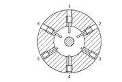
- FIG. 8 is a schematic diagram illustrating a one-dimensional equivalent circuit of electric lines of force illustrated in FIG. 7. It is sectional drawing of the coaxial waveguide provided in the plasma processing apparatus which concerns on one Embodiment of this invention, and provided six stub members, and shows the position of each stub member.
- FIG. 17 It is a figure which shows the relative energy integral value in each direction of a dielectric material board, and shows the time of the distance of the front-end
- FIG. 1 is a schematic sectional view showing a main part of a plasma processing apparatus according to an embodiment of the present invention.
- FIG. 2 is a schematic cross-sectional view showing an enlarged vicinity of the coaxial waveguide provided in the plasma processing apparatus shown in FIG.
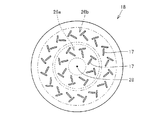
- FIG. 3 is a view of the slot antenna plate provided in the plasma processing apparatus shown in FIG. 1 as viewed from the direction of arrow III in FIG. 4 is a cross-sectional view of the coaxial waveguide provided in the plasma processing apparatus shown in FIG. 1 cut along IV-IV in FIG.
- the vertical direction of the paper is the vertical direction of the apparatus.
- the radial direction refers to the direction from the inner conductor to the outer conductor included in the coaxial waveguide in FIG.
- a plasma processing apparatus 11 is open on the upper side, and a processing container 12 that performs plasma processing on a substrate W to be processed therein, and a gas for plasma excitation in the processing container 12 And a gas supply unit 13 for supplying a gas for plasma processing, a holding base 14 that is disposed in the processing container 12 and holds the substrate W to be processed, and is disposed outside the processing container 12 for plasma excitation.
- a microwave generator 15 for generating microwaves a dielectric plate 16 disposed so as to cover the opening of the processing container 12 to seal the processing container 12 and transmit microwaves into the processing container 12, and a plurality of dielectric plates 16
- a slot antenna plate 18 which is disposed above the dielectric plate 16 and radiates microwaves to the dielectric plate 16, and a slot antenna plate.
- a slow wave plate 19 that propagates the microwave in the radial direction
- a microwave supply means 20 that supplies the microwave generated by the microwave generator 15 into the processing container 12, and a plasma treatment
- a control unit (not shown) for controlling the entire apparatus 11.
- the control unit controls process conditions for plasma processing the substrate W to be processed, such as a gas flow rate in the gas supply unit 13 and a pressure in the processing container 12.
- the microwave generator 15 is indicated by a one-dot chain line in FIG.
- the processing container 12 includes a bottom portion 21 located on the lower side of the holding table 14 and a side wall 22 extending upward from the outer peripheral portion of the bottom portion 21.
- the side wall 22 is cylindrical.
- An exhaust hole 23 for exhaust is provided on the center side in the radial direction of the bottom 21 of the processing container 12.
- the upper side of the processing vessel 12 is open, and is provided by a dielectric plate 16 disposed on the upper side of the processing vessel 12 and an O-ring 24 as a seal member interposed between the dielectric plate 16 and the processing vessel 12.
- the processing container 12 is configured to be sealable.
- a part of the gas supply unit 13 described above is provided so as to be embedded in the side wall 22, and gas is supplied into the processing container 12 from the outside of the processing container 12.
- the lower surface 25 of the dielectric plate 16 is flat.
- the material of the dielectric plate 16 is a dielectric. Specific examples of the material of the dielectric plate 16 include quartz and alumina.
- the both sides of the slot antenna plate 18 in the thickness direction are flat.
- the slot antenna plate 18 is provided with a plurality of slot holes 17 penetrating in the plate thickness direction.
- the slot hole 17 is configured by arranging a pair of two rectangular openings so as to be substantially T-shaped.
- the provided slot holes 17 are roughly divided into an inner peripheral slot hole group 26a disposed on the inner peripheral side and an outer peripheral slot hole group 26b disposed on the outer peripheral side.
- the inner peripheral side slot hole group 26a is eight slot holes 17 provided within a range surrounded by a dotted line in FIG.
- the outer peripheral side slot hole group 26b is 16 slot holes 17 provided in a range surrounded by a one-dot chain line in FIG.
- the eight slot holes 17 are annularly arranged at equal intervals.
- the 16 slot holes 17 are annularly arranged at equal intervals.
- the slot antenna plate 18 has rotational symmetry about the radial center 28, and, for example, has the same shape even when rotated 45 ° about the center 28.
- the slow wave plate 19 In the center of the slow wave plate 19, an opening for arranging an inner conductor 32 provided in a coaxial waveguide 31 to be described later is provided. An end portion on the inner diameter side of the slow wave plate 19 that forms the periphery of the opening protrudes in the thickness direction. That is, the slow wave plate 19 includes a ring-shaped slow wave plate projecting portion 27 that projects in the thickness direction from the end on the inner diameter side. The slow wave plate 19 is attached so that the slow wave plate protrusion 27 is on the upper side.
- the material of the slow wave plate 19 is a dielectric. Specific materials for the slow wave plate 19 include quartz and alumina. The wavelength of the microwave propagating inside the slow wave plate 19 is shorter than the wavelength of the microwave propagating in the atmosphere.
- the dielectric plate 16, the slot antenna plate 18, and the slow wave plate 19 are all disk-shaped.
- the radial center of the dielectric plate 16, the radial center 28 of the slot antenna plate 18, and the radial center of the slow wave plate 19 are made to coincide with each other. To be manufactured. By doing so, in the microwave propagated from the center side toward the outer diameter side, the propagation degree of the microwave in the circumferential direction is made the same, and the plasma generated in the lower side of the dielectric plate 16 is uniform in the circumferential direction. We are trying to ensure sex.
- the radial center 28 of the slot antenna plate 18 is used as a reference.
- the microwave supply means 20 includes an inner conductor 32 having a substantially round bar shape whose one end 35 is connected to the center 28 of the slot antenna plate 18, and an outer diameter of the inner conductor 32 by opening a radial gap 34 with the inner conductor 32.
- a coaxial waveguide 31 including a substantially cylindrical outer conductor 33 provided on the side is provided. That is, the coaxial waveguide 31 is configured by combining the inner conductor 32 and the outer conductor 33 so that the outer peripheral surface 36 of the inner conductor 32 and the inner peripheral surface 37 of the outer conductor 33 face each other.
- the coaxial waveguide 31 is provided so as to extend in the vertical direction of the drawing in FIG.
- Each of the inner conductor 32 and the outer conductor 33 is manufactured separately. Then, the inner conductor 32 and the outer conductor 33 are combined so that the radial center of the inner conductor 32 coincides with the radial center of the outer conductor 33.
- the microwave supply means 20 includes a waveguide 39 whose one end 38 is connected to the microwave generator 15 and a mode converter 40 for converting the mode of the microwave.
- the waveguide 39 is provided so as to extend in the horizontal direction, specifically, in the left-right direction in FIG.
- a waveguide having a circular cross section or a rectangular cross section is used as the waveguide 39.
- FIG. 16 is a schematic diagram showing the configuration of the microwave generator 15.
- the microwave generator 15 is provided on the most upstream side with a magnetron 29a that generates microwaves and on the downstream side of the magnetron 29a, and supplies the microwaves generated by the magnetron 29a to the downstream side.
- the isolator 29b for removing the reflected wave reflected from the downstream side and the phase of the microwave when the microwave generated by the magnetron 29a is propagated downstream are arranged on the downstream side of the isolator 29b.
- 4E tuner 29c as a matching unit for adjusting the frequency.
- the direction in which the microwave is propagated is from upstream to downstream.
- the magnetron 29a is positioned on the most upstream side, and is located downstream in the order of the isolator 29b and the 4E tuner 29c.
- the 4E tuner 29c is provided in the microwave propagation direction and is disposed inside each of the four recesses 30a, 30b, 30c, 30d and the four recesses 30a to 30d that are recessed from the waveguide toward the outer diameter side. It is configured to include four movable short-circuit plates 30e, 30f, 30g, and 30h that are movable in the radial direction and shaped to cover the recesses 30a to 30d.
- the radial direction here is the vertical direction in FIG.
- the four movable short-circuit plates 30e to 30h are respectively moved in the radial direction, and the phase of the microwave propagating in the waveguide 39 is adjusted.
- the left end 30i in FIG. 16 is connected to the end 38 in FIG.
- the microwave generated in the microwave generator 15 is propagated into the processing container 12 through the waveguide 39 and the coaxial waveguide 31.
- microwaves of TE mode which is generated by the microwave generator 15 propagates in the left direction in the drawing showing the the waveguide 39 by the arrow A 1 in FIG. 1, the mode converter 40 is converted into a TEM mode The Then, the microwave is converted into a TEM mode propagates through the coaxial waveguide 31 to the paper surface under the direction indicated by arrow A 2 in Fig. Specifically, the microwave propagates between the inner conductor 32 and the outer conductor 33 where the gap 34 is formed, and between the inner conductor 32 and the cooling plate protrusion 47.
- the microwave propagated through the coaxial waveguide 31 propagates in the radial direction in the slow wave plate 19 and is radiated to the dielectric plate 16 from a plurality of slot holes 17 provided in the slot antenna plate 18.
- the microwave transmitted through the dielectric plate 16 generates an electric field directly below the dielectric plate 16 and generates plasma in the processing container 12.
- the plasma processing apparatus 11 is disposed on the upper side of the upper end portion on the opening side of the side wall 22, and on the upper side of the dielectric plate pressing ring 41 and the dielectric plate pressing ring 41 for pressing the dielectric plate 16 from the upper side.
- An antenna holder 42 that holds the slot antenna plate 18 and the like from above, a cooling plate 43 that is arranged above the slow wave plate 19 and cools the slow wave plate 19, and the antenna holder 42 and cooling plate 43.
- the electromagnetic shielding elastic body 44 that shields the electromagnetic field inside and outside the processing container 12, the outer peripheral fixing ring 45 that fixes the outer peripheral portion of the slot antenna plate 18, and the center of the slot antenna plate 18. And a center fixing plate 46 to be fixed.
- An opening for arranging the coaxial waveguide 31 is provided in the center of the cooling plate 43.
- An end portion on the inner diameter side of the cooling plate 43 forming the periphery of the opening protrudes in the plate thickness direction. That is, the cooling plate 43 includes a ring-shaped cooling plate protrusion 47 that protrudes in the plate thickness direction from the end portion on the inner diameter side. The cooling plate 43 is attached so that the cooling plate protrusion 47 is on the upper side.
- a cylindrical outer conductor 33 is disposed above the cooling plate protrusion 47.
- the upper end of the cooling plate protrusion 47 and the lower end of the outer conductor 33 are in contact with each other.
- the inner circumferential surface 37 of the outer conductor 33 and the inner circumferential surface 50 of the cooling plate protrusion 47 are continuous, and the radial distance between the outer circumferential surface 36 of the inner conductor 32 and the inner circumferential surface 37 of the outer conductor 33, The radial distance between the outer peripheral surface 36 of the inner conductor 32 and the inner peripheral surface 50 of the cooling plate protrusion 47 is the same.
- a gap 34 formed between the inner conductor 32 and the outer conductor 33 is positioned above the above-described slow wave plate protrusion 27.
- a slow wave plate positioning portion 48 protruding in a ring shape on the dielectric plate 16 side is provided on the outer peripheral portion of the cooling plate 43.
- the slow wave plate 19 is positioned in the radial direction by the slow wave plate positioning portion 48.
- the outer peripheral fixing ring 45 fixes the slot antenna plate 18 at the radial position where the slow wave plate positioning portion 48 is provided.
- a receiving recess that is recessed so as to reduce the plate thickness from the upper surface of the dielectric plate 16 so as to receive the center fixing plate 46 in the center in the radial direction. 49 is provided.
- the microwave supply means 20 has a diameter of a part of the outer peripheral surface 36 of the inner conductor 32 and a facing part that opposes a part of the outer peripheral surface of the inner conductor 32 in the radial direction, here the cooling plate protrusion 47.
- a stub member 51 that can extend from the outer conductor 33 side toward the inner conductor 32 side is provided.
- the stub member 51 includes a rod-like portion 52 that is supported on the outer conductor 33 side and is provided so as to extend in the radial direction, and a screw portion 53 as a movement amount adjusting member that adjusts the movement amount of the rod-like portion 52 in the radial direction.
- the threaded portion 53 is provided at the outer diameter side end of the rod-shaped portion 52.
- the stub member 51 is attached to the cooling plate protrusion 47.
- the cooling plate protruding portion 47 is provided with a screw hole 54 that extends straight through in the radial direction and penetrates the stub member so that the screw hole 54 and the screw portion 53 are screwed together.
- 51 is attached to the cooling plate protrusion 47. That is, the stub member 51 is supported on the outer conductor 33 side by the screw portion 53 that is screwed into the screw hole 54 provided in the cooling plate protrusion 47.
- the entire stub member 51 including the rod-like part 52 can be moved in the radial direction.
- the stub member 51 is movable in the left-right direction on the paper surface. The amount of movement is adjusted by the amount of rotation of the screw portion 53.
- a total of six stub members 51 are provided so as to be substantially equidistant in the circumferential direction (see FIG. 4). That is, the six stub members are arranged such that the angle between adjacent stub members in the circumferential direction is 60 °.
- the six stub members 51 can move independently in the radial direction. That is, the radial position of the distal end portion 55 of the rod-like portion 52 included in each stub member 51 can be adjusted separately.
- the outer circumference of the inner conductor in the radial direction and part of the outer circumference of the inner conductor is adjusted by changing means that changes the radial distance to the part facing the part of the surface.
- the plasma generated in the processing vessel is generated on the lower surface of the dielectric plate by eliminating the deviation in the circumferential direction of the electromagnetic field distribution formed on the dielectric plate due to the deviation between the center of the inner conductor and the center of the outer conductor. Can be uniform on the side. In this case, for example, it is possible to deal with a deviation in the circumferential direction of the electromagnetic field distribution caused by, for example, a mounting error of the slow wave plate. As a result, the processing within the surface of the substrate to be processed can be made uniform.
- the upper side is open, a processing container for performing plasma processing on the substrate to be processed in the inside, and a gas for supplying a plasma processing gas into the processing container
- a supply unit, a holding base for holding a substrate to be processed, a microwave generator for generating a microwave for plasma excitation, and a processing container are arranged to cover the opening of the processing container.
- a dielectric plate that seals the processing vessel and transmits microwaves into the processing vessel and a plurality of slot holes are provided, and is disposed above the dielectric plate to radiate microwaves to the dielectric plate.
- a slot antenna plate a slow wave plate that is disposed above the slot antenna plate and propagates microwaves in the radial direction, and a microwave generated by the microwave generator
- a microwave supply means for supplying to the plate, the microwave supply means having a radially round gap between an inner conductor and an inner conductor of a substantially round bar shape whose one end is connected to the center of the slot antenna plate.
- a coaxial waveguide including a substantially cylindrical outer conductor provided on the outer diameter side of the conductor, and a diameter between a portion of the outer peripheral surface of the inner conductor and a portion facing the outer peripheral surface of the inner conductor in the radial direction.
- a plasma processing apparatus having a changing means for changing the direction distance is prepared, a substrate to be processed is held on a holding table, a microwave is generated by a microwave generator, and a part of the outer peripheral surface of the inner conductor is generated by the changing means.
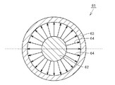
- FIG. 5 is a schematic diagram showing lines of electric force in a conventional coaxial waveguide not provided with a stub member.
- 6 is a conceptual diagram showing a one-dimensional equivalent circuit of the electric force lines shown in FIG. 5 on the dotted line shown in FIG.
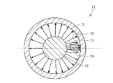
- FIG. 7 is a schematic diagram showing lines of electric force in the coaxial waveguide according to the present invention provided with a stub member.
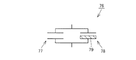
- FIG. 8 is a conceptual diagram showing a one-dimensional equivalent circuit of the electric force lines shown in FIG. 7 on the dotted line shown in FIG.
- the total number of lines of electric force described above is due to the power of the microwave. Further, from the viewpoint of easy understanding, only the inner conductor and the outer conductor included in the coaxial waveguide are shown.
- the electric lines of force 64 extending from the inner conductor 62 toward the outer conductor 63 in the coaxial waveguide 61 are uniform in the circumferential direction. Also in the primary equivalent circuit 65, the capacitances of the left and right capacitors 66 and 67 are the same. Such electric lines of force 64 are generated when the radial center of the inner conductor 62 and the radial center of the outer conductor 63 substantially coincide with each other.
- the radial center of the inner conductor 62 and the radial center of the outer conductor 63 deviate, the balance of the electric lines of force 64 described above is lost. As a result, the uniformity of the generated plasma in the circumferential direction is impaired.
- the radial center of the inner conductor 62 and the radial center of the outer conductor 63 substantially coincide with each other. There is no choice but to reassemble. Specifically, the length dimension X indicating the deviation between the radial centers shown in FIG. 15 is at a level of 0.01 mm.
- the radial center of the inner conductor 72 and the radial center of the outer conductor 73 are the same.
- the distance of the radial direction of the stub member 74 is changed. If there is a portion with a short radial distance between the outer circumferential surface of the inner conductor 72 and another member, here, the stub member 74, the electric lines of force 75 are concentrated on that portion.
- the capacitance of the right capacitor 78 is larger than that of the left capacitor 77 due to the influence of the stub member 74 indicated by hatching 79 in FIG. Therefore, the amount of radial movement of the stub member 74, specifically, the radial distance between the outer peripheral surface of the inner conductor 72 and the stub member 74 is changed, and the balance of the electric lines of force 75 in the circumferential direction is adjusted. This ensures the uniformity of the generated plasma in the circumferential direction.
- FIG. 9 is a cross-sectional view of the coaxial waveguide, showing the position of each stub member.
- the cross section shown in FIG. 9 corresponds to a view obtained by rotating the cross section shown in FIG. 4 by 90 degrees counterclockwise.
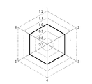
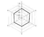
- 10, FIG. 11, FIG. 12 and FIG. 13 are diagrams showing relative energy integration values based on simulation results in each direction of the dielectric plate. Specifically, the numerical values in the radial direction in FIGS. 10 to 13 are obtained by dividing the dielectric plate into six regions in the circumferential direction, calculating the electric field intensity energy integrated value in each region, and calculating the electric field intensity energy integrated value in each region.
- the slot holes are arranged using a rotationally symmetric model that has the same shape even when rotated by 60 °.
- the rotational symmetry of the slot holes and the rotational symmetry of the stub member are not necessarily the same. It doesn't have to be the same.
- FIG. 9 shows a case where the positions of all the stub members are the same, and serves as a reference.
- FIG. 11 shows a case where the distance between the tip of the stub members numbered 1, 2, and 3 and the outer peripheral surface of the inner conductor is 6 mm.
- FIG. 12 shows a case where the distance between the tip of the stub members of Nos.
- FIG. 13 shows a case where the distance between the tip of the stub members numbered 1, 2, and 3 and the outer peripheral surface of the inner conductor is 2 mm.
- the value of 1 ⁇ in FIG. 10 is 0.8%
- the value of 1 ⁇ in FIG. 11 is 1.9%
- the value of 1 ⁇ in FIG. 12 is 3.8%
- 1 ⁇ in FIG. The value of is 7.6%.
- (sigma) shows a standard deviation.
- the relative energy integrated value in the dielectric plate is changed. It changes a lot.
- the stub member is moved in the radial direction even when the radial center of the inner conductor is shifted from the radial center of the outer conductor during manufacturing and the relative energy integrated value is significantly different from that shown in FIG.
- the relative energy integral value in each region can be adjusted. And even if it does not reassemble an inner conductor and an outer conductor, it can approximate to the reference
- the stub member As a material of the stub member, it is preferable that at least a portion of the stub member that can be positioned in the gap is a dielectric. By doing so, the life of the stub member can be extended. Examples of the dielectric include quartz and alumina. Of course, the entire stub member may be made of metal.
- the distance between the upper end of the slow wave plate and the stub member is preferably within 10 mm.
- the axial distance L 1 between 57 be within 10 mm.
- the plasma processing apparatus 11 having the above-described configuration is strongly influenced by the electromagnetic field intensity distribution in the lower region of the coaxial waveguide 31.
- the distance L 1 is longer than 10 mm, the strength of the asymmetric with microwave in the circumferential direction is again symmetrical, i.e., there is a possibility that returning to the original. Therefore, with this configuration, the electromagnetic field distribution can be made more uniform in the circumferential direction more efficiently.
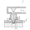
- FIG. 14 is an enlarged schematic cross-sectional view showing the vicinity of the coaxial waveguide of the plasma processing apparatus in this case, and corresponds to FIG.
- the cooling plate protrusion 83 of the cooling plate 82 provided in the plasma processing apparatus 81 according to another embodiment of the present invention is cooled so as to extend obliquely downward with the inner diameter side as the lower side.
- a plurality of screw holes 84 penetrating a part of the plate protrusion 83 are provided.
- the stub member 85 is attached so that it may extend in the diagonally downward direction.
- the point at which the stub member 85 acts specifically, the tip portion of the stub member 85 can be brought closer to the slow wave plate 19.
- the electromagnetic field distribution can be adjusted as close to the retardation plate 19 as possible. Therefore, by providing the stub member 85 so as to extend obliquely downward, the electromagnetic field distribution can be adjusted more effectively in the circumferential direction.
- the stub member 85 and the slow wave plate 86 have a distance L between the front end portion 87 of the stub member 85 and the upper end portion 89 of the slow wave plate projection 88 when the stub member 85 is extended. 3 may be 10 mm or less.
- the changing means may be configured such that a radial distance between a part of the outer peripheral surface of the inner conductor and a part facing the part can be changed to 4 mm or less. preferable.
- the outer peripheral surface 36 of the inner conductor 32 capable of changing the radial distance L 2 between the tip portion 55 of the rod portion 52 provided in the stub member 51, to 4mm below Configure as follows. By doing so, plasma uniformity in the circumferential direction can be improved in a wider category.
- the stub member is supported by the cooling plate protrusion, but is not limited thereto, and may be supported by an outer conductor. Specifically, a screw hole penetrating in the radial direction is provided in the outer conductor, and the stub member is attached so that the screw hole and the screw portion are screwed together. In this case, a facing portion that faces a part of the outer peripheral surface of the inner conductor becomes a part of the inner peripheral surface of the outer conductor.
- the stub members are arranged at equal intervals having rotational symmetry.
- the arrangement of the stub members may not be equal as long as it has rotational symmetry.
- a total of six stub members are provided in the circumferential direction.
- the number of stub members is not limited to this.
- four or eight stub members may be provided as required.
- a member is provided.
- one stub member is provided in the extending direction of the coaxial waveguide, that is, in the same position in the vertical direction.
- a plurality of coaxial waveguides may be provided at intervals in the extending direction.
- the influence of the reflected wave by the stub seat is greatly reduced, the adjustment of the electromagnetic field is facilitated, and the electromagnetic field distribution is changed in the circumferential direction. Can be made more uniform.
- FIG. 17 is a cross-sectional view showing a part of the plasma processing apparatus in this case, which corresponds to FIG.
- a plasma processing apparatus 91 according to still another embodiment of the present invention is provided with two stub member groups 92a and 92b in the vertical direction in FIG.
- the first stub member group 92a as the electromagnetic field adjustment mechanism provided on the lower side is provided on the cooling plate protrusion 47 of the cooling plate 43, similarly to the case of being provided in the plasma processing apparatus 11 shown in FIG. ing.
- Each stub member in the first stub member group 92a has the same configuration as the stub member provided in the plasma processing apparatus shown in FIG.
- each stub member included in the first stub member group 92a can extend in the radial direction, extends straight in the radial direction, and is screwed into a screw hole provided in the cooling plate protrusion 47. It is a structure provided with the thread part and rod-shaped part which were provided in.
- the second stub member group 92 b as the reflected wave compensation mechanism provided on the upper side is provided on the outer conductor 33 of the coaxial waveguide 31.
- Each stub member provided in the second stub member group 92b has the same configuration as each stub member provided in the first stub member group 92a, can extend in the radial direction, and is straight in the radial direction. And a screw portion and a rod-like portion provided so as to be screwed into a screw hole provided in the outer conductor 33.
- the first stub member group 92a is provided with six stub members substantially equally spaced in the circumferential direction as in the case shown in FIG.
- the second stub member group 92b is also provided with six stub members that are substantially equally spaced in the circumferential direction.
- the two stub member groups referred to here are a group of stub members composed of six stub members provided at intervals in the circumferential direction, and are provided at intervals in the vertical direction. It means that.
- each stub member of the 1st stub member group 92a and the 2nd stub member group 92b is configured to be at the same position. That is, when viewed from above in FIG. 17, it looks as shown in FIG. 4, and each stub member in the first stub member group 92a and each stub member in the second stub member group 92b. It is configured so that and appear to overlap.
- the coaxial waveguide 31 is configured to be a quarter of the in-tube wavelength.
- each stub member provided in the first stub member group 92a and the microwave reflectance of each stub member provided in the second stub member group 92b are the same.
- the material of each stub member provided in the first and second stub member groups 92a and 92b is, for example, alumina or metal.
- the first stub member group 92a that functions as an electromagnetic field adjustment mechanism and the second stub member group 92b that functions as a reflected wave compensation mechanism can more efficiently uniformize the electromagnetic field distribution. can do.
- FIG. 18 is a schematic cross-sectional view showing an enlarged vicinity of the coaxial waveguide 31 provided in the plasma processing apparatus 91 shown in FIG. From the viewpoint of easy understanding, FIG. 18 schematically shows the configuration of the first and second stub member groups 92a and 92b.
- the incident wave C 1 incident from the upper side to the lower direction reaches the stub member provided in the first stub member group 92 a as the electromagnetic field adjustment mechanism, part is reflected upward as a reflected wave C 2.
- the incident wave D 1 is after reaching the stub member provided in the second stub member group 92b as a reflection wave compensation mechanism, a portion is reflected upward as a reflected wave D 2.
- interfering reflected waves C 2 to an amount corresponding time round-trip journey distance L 4 is delayed between the first stub member group 92a and the second stub member group 92b is a reflection wave D 2.
- the first stub member group 92a and the second stub member group 92b are a quarter of the guide wavelength of the coaxial waveguide 31.
- the first stub member group The reciprocating path of the distance between 92a and the second stub member group 92b is a half of the in-tube wavelength of the coaxial waveguide 31.
- the phases of the respective reflected waves C 2 and D 2 are shifted by 180 degrees.
- the reflectance in the stub member provided in the first stub member group 92a and the reflectance in the stub member provided in the second stub member group 92b are the same, the reflected waves C 2 and D 2 are exactly the same.
- the electromagnetic fields can be adjusted with greatly reduced influence of the reflected wave. Therefore, the electromagnetic field can be supplied more efficiently and uniformly.
- the 4E tuner 29c provided in the microwave generator 15 and including the movable short-circuit plates 30e to 30h is provided in the waveguide 39 and simply adjusts the phase of the microwave generated by the magnetron 29a.
- the configuration of the member group 92b is greatly different.
- the reflectance of the stub member provided in the first stub member group 92a and the reflectance of the stub member provided in the second stub member group 92b are set to be the same, but according to a specific embodiment.
- the respective reflectances are 0.1 to 0.2, and the reflectance can be 0.03 or less as a total.
- the incident wave C 1 above is smaller partially reflected by the stub member provided in the second stub member group 92b. Therefore, in consideration of this influence, the reflectance of the stub member provided in the first stub member group 92a and the reflectance of the stub member provided in the second stub member group 92b may be changed.
- the vertical distance between the first stub member group and the second stub member group is set to one quarter of the in-tube wavelength of the coaxial waveguide.
- the present invention is not limited to this, and may be an odd multiple of one-fourth of the guide wavelength of the coaxial waveguide.
- the phase of each reflected wave can be shifted by 180 degrees, and the above-described effects can be achieved.
- the influence of the reflected wave can be reduced even if it is slightly deviated from an odd multiple of 1/4 of the in-tube wavelength of the coaxial waveguide.
- each stub member with which a 1st stub member group is equipped and the circumferential position of each stub member with which a 2nd stub member group is equipped
- the present invention is not limited to this, and it may be slightly shifted in the circumferential direction.
- the number of stub members provided in the first stub member group may be different from the number of stub members provided in the second stub member group.
- the stub members included in the first and second stub member groups are provided so as to extend straight in the radial direction. You may decide to make the extending
- the extending direction may be an obliquely downward direction, and both the first and second stub member groups may be used.
- the extending direction may be a diagonally downward direction.
- the stub member is used as the changing unit.
- the changing unit is not limited to this, and another configuration may be used. That is, for example, on the inner peripheral surface of the outer conductor, a protrusion that can extend in the radial direction and can adjust the extension distance may be provided, and this may be used as the changing means. If the outer diameter surface of the outer conductor is recessed, the distance between the inner peripheral surface of the outer conductor and the outer peripheral surface of the inner conductor may be changed according to the recess.
- the changing means is provided on the outer conductor side.
- the changing means is not limited to this, and the changing means may be provided on the inner conductor side.
- the changing means can extend the outer peripheral surface of the inner conductor toward the outer diameter side, that is, the direction in which the gap is formed, and the extension distance can be adjusted.
- the configuration Such a configuration may be adopted.
- the lower surface of the dielectric plate is flattened.
- the present invention is not limited to this.
- the inner side of the dielectric plate Alternatively, a concave portion that is recessed upward may be provided.
- the plasma processing apparatus according to the present invention is effectively used when uniform processing is required within the surface of the substrate to be processed during plasma processing.
Landscapes
- Chemical & Material Sciences (AREA)
- Engineering & Computer Science (AREA)
- Physics & Mathematics (AREA)
- Plasma & Fusion (AREA)
- Analytical Chemistry (AREA)
- Materials Engineering (AREA)
- Metallurgy (AREA)
- Organic Chemistry (AREA)
- Mechanical Engineering (AREA)
- Chemical Kinetics & Catalysis (AREA)
- General Chemical & Material Sciences (AREA)
- Electromagnetism (AREA)
- Spectroscopy & Molecular Physics (AREA)
- Plasma Technology (AREA)
- Chemical Vapour Deposition (AREA)
- Drying Of Semiconductors (AREA)
Abstract
Description
Claims (11)
- 上部側が開口しており、その内部において被処理基板にプラズマ処理を行う処理容器と、
前記処理容器内にプラズマ処理用のガスを供給するガス供給部と、
前記処理容器内に配置され、その上に前記被処理基板を保持する保持台と、
プラズマ励起用のマイクロ波を発生させるマイクロ波発生器と、
前記処理容器の開口を覆うように配置されて前記処理容器を密封すると共に、マイクロ波を前記処理容器内へ透過させる誘電体板と、
複数のスロット孔が設けられており、前記誘電体板の上方側に配置され、マイクロ波を前記誘電体板に放射するスロットアンテナ板と、
前記スロットアンテナ板の上方側に配置され、マイクロ波を径方向に伝播させる遅波板と、
前記マイクロ波発生器により発生させたマイクロ波を前記スロットアンテナ板に供給するマイクロ波供給手段とを備え、
前記マイクロ波供給手段は、一方端部が前記スロットアンテナ板の中心に接続される略丸棒状の内導体および前記内導体との径方向のすき間を開けて前記内導体の外径側に設けられる略円筒状の外導体を含む同軸導波管、および前記内導体の外周面の一部と径方向において前記内導体の外周面の一部に対向する対向部との径方向の距離を変更させる変更手段を備える、プラズマ処理装置。 - 前記変更手段は、前記外導体側から前記内導体側へ向かって延出可能なスタブ部材を含む、請求項1に記載のプラズマ処理装置。
- 前記スタブ部材は、前記外導体側で支持され、径方向に延びるように設けられる棒状部と、前記棒状部の径方向の移動量を調整する移動量調整部材とを含む、請求項2に記載のプラズマ処理装置。
- 前記スタブ部材は、前記同軸導波管が延びる方向に間隔を開けて複数設けられる、請求項2に記載のプラズマ処理装置。
- 前記スタブ部材は、周方向に間隔を開けて複数設けられる、請求項2に記載のプラズマ処理装置。
- 前記複数のスタブ部材は、周方向に略等配に設けられる、請求項5に記載のプラズマ処理装置。
- 前記スタブ部材のうち、少なくとも前記すき間に位置可能な部分の材質は、誘電体である、請求項2に記載のプラズマ処理装置。
- 前記同軸導波管における軸方向において、前記遅波板の上方側の端部と前記スタブ部材との距離は、10mm以下である、請求項2に記載のプラズマ処理装置。
- 前記変更手段は、前記内導体の外周面の一部と前記一部に対向する対向部との径方向の距離を、4mm以下に変更可能である、請求項1に記載のプラズマ処理装置。
- 前記マイクロ波発生器は、マグネトロンと、アイソレータと、チューナとを含む、請求項1に記載のプラズマ処理装置。
- 上部側が開口しており、その内部において被処理基板にプラズマ処理を行う処理容器と、前記処理容器内にプラズマ処理用のガスを供給するガス供給部と、前記処理容器内に配置され、その上に前記被処理基板を保持する保持台と、プラズマ励起用のマイクロ波を発生させるマイクロ波発生器と、前記処理容器の開口を覆うように配置されて前記処理容器を密封すると共に、マイクロ波を前記処理容器内へ透過させる誘電体板と、複数のスロット孔が設けられており、前記誘電体板の上方側に配置され、マイクロ波を前記誘電体板に放射するスロットアンテナ板と、前記スロットアンテナ板の上方側に配置され、マイクロ波を径方向に伝播させる遅波板と、前記マイクロ波発生器により発生させたマイクロ波を前記スロットアンテナ板に供給するマイクロ波供給手段とを備え、前記マイクロ波供給手段は、一方端部が前記スロットアンテナ板の中心に接続される略丸棒状の内導体および前記内導体との径方向のすき間を開けて前記内導体の外径側に設けられる略円筒状の外導体を含む同軸導波管、および前記内導体の外周面の一部と径方向において前記内導体の外周面の一部に対向する対向部との径方向の距離を変更させる変更手段を備えるプラズマ処理装置を準備し、
前記保持台に被処理基板を保持させ、
前記マイクロ波発生器によりマイクロ波を発生させ、
前記変更手段により、前記内導体の外周面の一部と径方向において前記内導体の外周面の一部に対向する対向部との径方向の距離を変更させて、前記処理容器内で発生させるプラズマを前記誘電体板の下面側において均一にして、前記被処理基板に対するプラズマ処理を行う、基板処理方法。
Priority Applications (5)
| Application Number | Priority Date | Filing Date | Title |
|---|---|---|---|
| JP2011527670A JP5440604B2 (ja) | 2009-08-21 | 2010-08-16 | プラズマ処理装置および基板処理方法 |
| US13/391,310 US9237638B2 (en) | 2009-08-21 | 2010-08-16 | Plasma processing apparatus and substrate processing method |
| KR1020127004461A KR101378304B1 (ko) | 2009-08-21 | 2010-08-16 | 플라즈마 처리 장치 및 기판 처리 방법 |
| CN2010800371514A CN102484939A (zh) | 2009-08-21 | 2010-08-16 | 等离子体处理装置和基板处理方法 |
| US14/956,471 US20160093474A1 (en) | 2009-08-21 | 2015-12-02 | Substrate processing method |
Applications Claiming Priority (2)
| Application Number | Priority Date | Filing Date | Title |
|---|---|---|---|
| JP2009191700 | 2009-08-21 | ||
| JP2009-191700 | 2009-08-21 |
Related Child Applications (2)
| Application Number | Title | Priority Date | Filing Date |
|---|---|---|---|
| US13/391,310 A-371-Of-International US9237638B2 (en) | 2009-08-21 | 2010-08-16 | Plasma processing apparatus and substrate processing method |
| US14/956,471 Division US20160093474A1 (en) | 2009-08-21 | 2015-12-02 | Substrate processing method |
Publications (1)
| Publication Number | Publication Date |
|---|---|
| WO2011021607A1 true WO2011021607A1 (ja) | 2011-02-24 |
Family
ID=43607058
Family Applications (1)
| Application Number | Title | Priority Date | Filing Date |
|---|---|---|---|
| PCT/JP2010/063831 Ceased WO2011021607A1 (ja) | 2009-08-21 | 2010-08-16 | プラズマ処理装置および基板処理方法 |
Country Status (6)
| Country | Link |
|---|---|
| US (2) | US9237638B2 (ja) |
| JP (1) | JP5440604B2 (ja) |
| KR (1) | KR101378304B1 (ja) |
| CN (1) | CN102484939A (ja) |
| TW (1) | TW201143545A (ja) |
| WO (1) | WO2011021607A1 (ja) |
Cited By (5)
| Publication number | Priority date | Publication date | Assignee | Title |
|---|---|---|---|---|
| WO2016104205A1 (ja) * | 2014-12-26 | 2016-06-30 | 東京エレクトロン株式会社 | プラズマ処理装置及びプラズマ処理方法 |
| JP2018078010A (ja) * | 2016-11-09 | 2018-05-17 | 東京エレクトロン株式会社 | マイクロ波プラズマ源およびマイクロ波プラズマ処理装置 |
| KR101915833B1 (ko) * | 2014-02-19 | 2018-11-06 | 도쿄엘렉트론가부시키가이샤 | 기판 처리 장치 |
| US10930477B2 (en) | 2017-12-13 | 2021-02-23 | Tokyo Electron Limited | Plasma processing apparatus |
| US11605528B2 (en) | 2019-07-09 | 2023-03-14 | Asm Ip Holding B.V. | Plasma device using coaxial waveguide, and substrate treatment method |
Families Citing this family (294)
| Publication number | Priority date | Publication date | Assignee | Title |
|---|---|---|---|---|
| JP2010118549A (ja) * | 2008-11-13 | 2010-05-27 | Tokyo Electron Ltd | プラズマエッチング方法及びプラズマエッチング装置 |
| US20130023129A1 (en) | 2011-07-20 | 2013-01-24 | Asm America, Inc. | Pressure transmitter for a semiconductor processing environment |
| WO2013098795A1 (en) * | 2011-12-29 | 2013-07-04 | Selex Galileo S.P.A. | Slotted waveguide antenna for near-field focalization of electromagnetic radiation |
| JP2014035887A (ja) * | 2012-08-09 | 2014-02-24 | Tokyo Electron Ltd | プラズマ処理装置、および高周波発生器 |
| US10714315B2 (en) | 2012-10-12 | 2020-07-14 | Asm Ip Holdings B.V. | Semiconductor reaction chamber showerhead |
| US20160376700A1 (en) | 2013-02-01 | 2016-12-29 | Asm Ip Holding B.V. | System for treatment of deposition reactor |
| US11015245B2 (en) | 2014-03-19 | 2021-05-25 | Asm Ip Holding B.V. | Gas-phase reactor and system having exhaust plenum and components thereof |
| US10858737B2 (en) | 2014-07-28 | 2020-12-08 | Asm Ip Holding B.V. | Showerhead assembly and components thereof |
| US10941490B2 (en) | 2014-10-07 | 2021-03-09 | Asm Ip Holding B.V. | Multiple temperature range susceptor, assembly, reactor and system including the susceptor, and methods of using the same |
| JP6501493B2 (ja) | 2014-11-05 | 2019-04-17 | 東京エレクトロン株式会社 | プラズマ処理装置 |
| US10276355B2 (en) | 2015-03-12 | 2019-04-30 | Asm Ip Holding B.V. | Multi-zone reactor, system including the reactor, and method of using the same |
| JP2016225047A (ja) * | 2015-05-27 | 2016-12-28 | 東京エレクトロン株式会社 | プラズマ処理装置 |
| US10458018B2 (en) | 2015-06-26 | 2019-10-29 | Asm Ip Holding B.V. | Structures including metal carbide material, devices including the structures, and methods of forming same |
| US10211308B2 (en) | 2015-10-21 | 2019-02-19 | Asm Ip Holding B.V. | NbMC layers |
| US11139308B2 (en) | 2015-12-29 | 2021-10-05 | Asm Ip Holding B.V. | Atomic layer deposition of III-V compounds to form V-NAND devices |
| US10529554B2 (en) | 2016-02-19 | 2020-01-07 | Asm Ip Holding B.V. | Method for forming silicon nitride film selectively on sidewalls or flat surfaces of trenches |
| US10343920B2 (en) | 2016-03-18 | 2019-07-09 | Asm Ip Holding B.V. | Aligned carbon nanotubes |
| US10367080B2 (en) | 2016-05-02 | 2019-07-30 | Asm Ip Holding B.V. | Method of forming a germanium oxynitride film |
| US11453943B2 (en) | 2016-05-25 | 2022-09-27 | Asm Ip Holding B.V. | Method for forming carbon-containing silicon/metal oxide or nitride film by ALD using silicon precursor and hydrocarbon precursor |
| US10182387B2 (en) | 2016-06-01 | 2019-01-15 | At&T Intellectual Property I, L.P. | Method and apparatus for distributing content via diverse networks |
| JP6683924B2 (ja) * | 2016-06-23 | 2020-04-22 | 東京エレクトロン株式会社 | プラズマ調整用の支援装置、プラズマ調整方法及び記憶媒体 |
| US10612137B2 (en) | 2016-07-08 | 2020-04-07 | Asm Ip Holdings B.V. | Organic reactants for atomic layer deposition |
| US9859151B1 (en) | 2016-07-08 | 2018-01-02 | Asm Ip Holding B.V. | Selective film deposition method to form air gaps |
| JP2018010752A (ja) * | 2016-07-12 | 2018-01-18 | 東京エレクトロン株式会社 | マイクロ波調整方法 |
| US9887082B1 (en) | 2016-07-28 | 2018-02-06 | Asm Ip Holding B.V. | Method and apparatus for filling a gap |
| KR102532607B1 (ko) | 2016-07-28 | 2023-05-15 | 에이에스엠 아이피 홀딩 비.브이. | 기판 가공 장치 및 그 동작 방법 |
| US9812320B1 (en) | 2016-07-28 | 2017-11-07 | Asm Ip Holding B.V. | Method and apparatus for filling a gap |
| US11532757B2 (en) | 2016-10-27 | 2022-12-20 | Asm Ip Holding B.V. | Deposition of charge trapping layers |
| US10714350B2 (en) | 2016-11-01 | 2020-07-14 | ASM IP Holdings, B.V. | Methods for forming a transition metal niobium nitride film on a substrate by atomic layer deposition and related semiconductor device structures |
| KR102546317B1 (ko) | 2016-11-15 | 2023-06-21 | 에이에스엠 아이피 홀딩 비.브이. | 기체 공급 유닛 및 이를 포함하는 기판 처리 장치 |
| KR102762543B1 (ko) | 2016-12-14 | 2025-02-05 | 에이에스엠 아이피 홀딩 비.브이. | 기판 처리 장치 |
| US11581186B2 (en) | 2016-12-15 | 2023-02-14 | Asm Ip Holding B.V. | Sequential infiltration synthesis apparatus |
| US11447861B2 (en) | 2016-12-15 | 2022-09-20 | Asm Ip Holding B.V. | Sequential infiltration synthesis apparatus and a method of forming a patterned structure |
| KR102700194B1 (ko) | 2016-12-19 | 2024-08-28 | 에이에스엠 아이피 홀딩 비.브이. | 기판 처리 장치 |
| US10269558B2 (en) | 2016-12-22 | 2019-04-23 | Asm Ip Holding B.V. | Method of forming a structure on a substrate |
| US11390950B2 (en) | 2017-01-10 | 2022-07-19 | Asm Ip Holding B.V. | Reactor system and method to reduce residue buildup during a film deposition process |
| JP6698560B2 (ja) * | 2017-02-01 | 2020-05-27 | 東京エレクトロン株式会社 | マイクロ波プラズマ源、マイクロ波プラズマ処理装置、およびプラズマ処理方法 |
| US10468261B2 (en) | 2017-02-15 | 2019-11-05 | Asm Ip Holding B.V. | Methods for forming a metallic film on a substrate by cyclical deposition and related semiconductor device structures |
| US10529563B2 (en) | 2017-03-29 | 2020-01-07 | Asm Ip Holdings B.V. | Method for forming doped metal oxide films on a substrate by cyclical deposition and related semiconductor device structures |
| US10770286B2 (en) | 2017-05-08 | 2020-09-08 | Asm Ip Holdings B.V. | Methods for selectively forming a silicon nitride film on a substrate and related semiconductor device structures |
| US12040200B2 (en) | 2017-06-20 | 2024-07-16 | Asm Ip Holding B.V. | Semiconductor processing apparatus and methods for calibrating a semiconductor processing apparatus |
| US11306395B2 (en) | 2017-06-28 | 2022-04-19 | Asm Ip Holding B.V. | Methods for depositing a transition metal nitride film on a substrate by atomic layer deposition and related deposition apparatus |
| JP2019012656A (ja) * | 2017-06-30 | 2019-01-24 | 東京エレクトロン株式会社 | プラズマ発生ユニット及びプラズマ処理装置 |
| KR20190009245A (ko) | 2017-07-18 | 2019-01-28 | 에이에스엠 아이피 홀딩 비.브이. | 반도체 소자 구조물 형성 방법 및 관련된 반도체 소자 구조물 |
| US10541333B2 (en) | 2017-07-19 | 2020-01-21 | Asm Ip Holding B.V. | Method for depositing a group IV semiconductor and related semiconductor device structures |
| US11374112B2 (en) | 2017-07-19 | 2022-06-28 | Asm Ip Holding B.V. | Method for depositing a group IV semiconductor and related semiconductor device structures |
| US11018002B2 (en) | 2017-07-19 | 2021-05-25 | Asm Ip Holding B.V. | Method for selectively depositing a Group IV semiconductor and related semiconductor device structures |
| US10590535B2 (en) | 2017-07-26 | 2020-03-17 | Asm Ip Holdings B.V. | Chemical treatment, deposition and/or infiltration apparatus and method for using the same |
| TWI815813B (zh) | 2017-08-04 | 2023-09-21 | 荷蘭商Asm智慧財產控股公司 | 用於分配反應腔內氣體的噴頭總成 |
| US10770336B2 (en) | 2017-08-08 | 2020-09-08 | Asm Ip Holding B.V. | Substrate lift mechanism and reactor including same |
| US10692741B2 (en) | 2017-08-08 | 2020-06-23 | Asm Ip Holdings B.V. | Radiation shield |
| US11769682B2 (en) | 2017-08-09 | 2023-09-26 | Asm Ip Holding B.V. | Storage apparatus for storing cassettes for substrates and processing apparatus equipped therewith |
| US11139191B2 (en) | 2017-08-09 | 2021-10-05 | Asm Ip Holding B.V. | Storage apparatus for storing cassettes for substrates and processing apparatus equipped therewith |
| US11830730B2 (en) | 2017-08-29 | 2023-11-28 | Asm Ip Holding B.V. | Layer forming method and apparatus |
| US11056344B2 (en) | 2017-08-30 | 2021-07-06 | Asm Ip Holding B.V. | Layer forming method |
| KR102491945B1 (ko) | 2017-08-30 | 2023-01-26 | 에이에스엠 아이피 홀딩 비.브이. | 기판 처리 장치 |
| US11295980B2 (en) | 2017-08-30 | 2022-04-05 | Asm Ip Holding B.V. | Methods for depositing a molybdenum metal film over a dielectric surface of a substrate by a cyclical deposition process and related semiconductor device structures |
| US10658205B2 (en) | 2017-09-28 | 2020-05-19 | Asm Ip Holdings B.V. | Chemical dispensing apparatus and methods for dispensing a chemical to a reaction chamber |
| US10403504B2 (en) | 2017-10-05 | 2019-09-03 | Asm Ip Holding B.V. | Method for selectively depositing a metallic film on a substrate |
| US10923344B2 (en) | 2017-10-30 | 2021-02-16 | Asm Ip Holding B.V. | Methods for forming a semiconductor structure and related semiconductor structures |
| JP6835358B2 (ja) * | 2017-11-24 | 2021-02-24 | 森田テック 株式会社 | アンテナ装置、アンテナシステム、及び計測システム |
| US11022879B2 (en) | 2017-11-24 | 2021-06-01 | Asm Ip Holding B.V. | Method of forming an enhanced unexposed photoresist layer |
| TWI791689B (zh) | 2017-11-27 | 2023-02-11 | 荷蘭商Asm智慧財產控股私人有限公司 | 包括潔淨迷你環境之裝置 |
| JP7214724B2 (ja) | 2017-11-27 | 2023-01-30 | エーエスエム アイピー ホールディング ビー.ブイ. | バッチ炉で利用されるウェハカセットを収納するための収納装置 |
| US10872771B2 (en) | 2018-01-16 | 2020-12-22 | Asm Ip Holding B. V. | Method for depositing a material film on a substrate within a reaction chamber by a cyclical deposition process and related device structures |
| KR102695659B1 (ko) | 2018-01-19 | 2024-08-14 | 에이에스엠 아이피 홀딩 비.브이. | 플라즈마 보조 증착에 의해 갭 충진 층을 증착하는 방법 |
| TWI799494B (zh) | 2018-01-19 | 2023-04-21 | 荷蘭商Asm 智慧財產控股公司 | 沈積方法 |
| DE102018000401A1 (de) * | 2018-01-19 | 2019-07-25 | Ralf Spitzl | Mikrowellenplasmavorrichtung |
| US11081345B2 (en) | 2018-02-06 | 2021-08-03 | Asm Ip Holding B.V. | Method of post-deposition treatment for silicon oxide film |
| US11685991B2 (en) | 2018-02-14 | 2023-06-27 | Asm Ip Holding B.V. | Method for depositing a ruthenium-containing film on a substrate by a cyclical deposition process |
| US10896820B2 (en) | 2018-02-14 | 2021-01-19 | Asm Ip Holding B.V. | Method for depositing a ruthenium-containing film on a substrate by a cyclical deposition process |
| US10731249B2 (en) | 2018-02-15 | 2020-08-04 | Asm Ip Holding B.V. | Method of forming a transition metal containing film on a substrate by a cyclical deposition process, a method for supplying a transition metal halide compound to a reaction chamber, and related vapor deposition apparatus |
| KR102636427B1 (ko) | 2018-02-20 | 2024-02-13 | 에이에스엠 아이피 홀딩 비.브이. | 기판 처리 방법 및 장치 |
| US10975470B2 (en) | 2018-02-23 | 2021-04-13 | Asm Ip Holding B.V. | Apparatus for detecting or monitoring for a chemical precursor in a high temperature environment |
| US11473195B2 (en) | 2018-03-01 | 2022-10-18 | Asm Ip Holding B.V. | Semiconductor processing apparatus and a method for processing a substrate |
| US11629406B2 (en) | 2018-03-09 | 2023-04-18 | Asm Ip Holding B.V. | Semiconductor processing apparatus comprising one or more pyrometers for measuring a temperature of a substrate during transfer of the substrate |
| US11114283B2 (en) | 2018-03-16 | 2021-09-07 | Asm Ip Holding B.V. | Reactor, system including the reactor, and methods of manufacturing and using same |
| KR102646467B1 (ko) | 2018-03-27 | 2024-03-11 | 에이에스엠 아이피 홀딩 비.브이. | 기판 상에 전극을 형성하는 방법 및 전극을 포함하는 반도체 소자 구조 |
| US11230766B2 (en) | 2018-03-29 | 2022-01-25 | Asm Ip Holding B.V. | Substrate processing apparatus and method |
| US11088002B2 (en) | 2018-03-29 | 2021-08-10 | Asm Ip Holding B.V. | Substrate rack and a substrate processing system and method |
| KR102600229B1 (ko) | 2018-04-09 | 2023-11-10 | 에이에스엠 아이피 홀딩 비.브이. | 기판 지지 장치, 이를 포함하는 기판 처리 장치 및 기판 처리 방법 |
| TWI843623B (zh) | 2018-05-08 | 2024-05-21 | 荷蘭商Asm Ip私人控股有限公司 | 藉由循環沉積製程於基板上沉積氧化物膜之方法及相關裝置結構 |
| US12025484B2 (en) | 2018-05-08 | 2024-07-02 | Asm Ip Holding B.V. | Thin film forming method |
| US12272527B2 (en) | 2018-05-09 | 2025-04-08 | Asm Ip Holding B.V. | Apparatus for use with hydrogen radicals and method of using same |
| KR102596988B1 (ko) | 2018-05-28 | 2023-10-31 | 에이에스엠 아이피 홀딩 비.브이. | 기판 처리 방법 및 그에 의해 제조된 장치 |
| US11718913B2 (en) | 2018-06-04 | 2023-08-08 | Asm Ip Holding B.V. | Gas distribution system and reactor system including same |
| TWI840362B (zh) | 2018-06-04 | 2024-05-01 | 荷蘭商Asm Ip私人控股有限公司 | 水氣降低的晶圓處置腔室 |
| US11286562B2 (en) | 2018-06-08 | 2022-03-29 | Asm Ip Holding B.V. | Gas-phase chemical reactor and method of using same |
| KR102568797B1 (ko) | 2018-06-21 | 2023-08-21 | 에이에스엠 아이피 홀딩 비.브이. | 기판 처리 시스템 |
| US10797133B2 (en) | 2018-06-21 | 2020-10-06 | Asm Ip Holding B.V. | Method for depositing a phosphorus doped silicon arsenide film and related semiconductor device structures |
| US11499222B2 (en) | 2018-06-27 | 2022-11-15 | Asm Ip Holding B.V. | Cyclic deposition methods for forming metal-containing material and films and structures including the metal-containing material |
| TWI871083B (zh) | 2018-06-27 | 2025-01-21 | 荷蘭商Asm Ip私人控股有限公司 | 用於形成含金屬材料之循環沉積製程 |
| US10612136B2 (en) | 2018-06-29 | 2020-04-07 | ASM IP Holding, B.V. | Temperature-controlled flange and reactor system including same |
| US10388513B1 (en) | 2018-07-03 | 2019-08-20 | Asm Ip Holding B.V. | Method for depositing silicon-free carbon-containing film as gap-fill layer by pulse plasma-assisted deposition |
| US10755922B2 (en) | 2018-07-03 | 2020-08-25 | Asm Ip Holding B.V. | Method for depositing silicon-free carbon-containing film as gap-fill layer by pulse plasma-assisted deposition |
| US11053591B2 (en) | 2018-08-06 | 2021-07-06 | Asm Ip Holding B.V. | Multi-port gas injection system and reactor system including same |
| US11430674B2 (en) | 2018-08-22 | 2022-08-30 | Asm Ip Holding B.V. | Sensor array, apparatus for dispensing a vapor phase reactant to a reaction chamber and related methods |
| US11024523B2 (en) | 2018-09-11 | 2021-06-01 | Asm Ip Holding B.V. | Substrate processing apparatus and method |
| KR102707956B1 (ko) | 2018-09-11 | 2024-09-19 | 에이에스엠 아이피 홀딩 비.브이. | 박막 증착 방법 |
| US11049751B2 (en) | 2018-09-14 | 2021-06-29 | Asm Ip Holding B.V. | Cassette supply system to store and handle cassettes and processing apparatus equipped therewith |
| CN110970344B (zh) | 2018-10-01 | 2024-10-25 | Asmip控股有限公司 | 衬底保持设备、包含所述设备的系统及其使用方法 |
| US11232963B2 (en) | 2018-10-03 | 2022-01-25 | Asm Ip Holding B.V. | Substrate processing apparatus and method |
| KR102592699B1 (ko) | 2018-10-08 | 2023-10-23 | 에이에스엠 아이피 홀딩 비.브이. | 기판 지지 유닛 및 이를 포함하는 박막 증착 장치와 기판 처리 장치 |
| KR102605121B1 (ko) | 2018-10-19 | 2023-11-23 | 에이에스엠 아이피 홀딩 비.브이. | 기판 처리 장치 및 기판 처리 방법 |
| KR102546322B1 (ko) | 2018-10-19 | 2023-06-21 | 에이에스엠 아이피 홀딩 비.브이. | 기판 처리 장치 및 기판 처리 방법 |
| USD948463S1 (en) | 2018-10-24 | 2022-04-12 | Asm Ip Holding B.V. | Susceptor for semiconductor substrate supporting apparatus |
| CN111101113A (zh) * | 2018-10-25 | 2020-05-05 | 六晶科技有限公司 | 微波等离子体cvd装置及利用其合成金刚石的方法 |
| US12378665B2 (en) | 2018-10-26 | 2025-08-05 | Asm Ip Holding B.V. | High temperature coatings for a preclean and etch apparatus and related methods |
| US11087997B2 (en) | 2018-10-31 | 2021-08-10 | Asm Ip Holding B.V. | Substrate processing apparatus for processing substrates |
| KR102748291B1 (ko) | 2018-11-02 | 2024-12-31 | 에이에스엠 아이피 홀딩 비.브이. | 기판 지지 유닛 및 이를 포함하는 기판 처리 장치 |
| US11572620B2 (en) | 2018-11-06 | 2023-02-07 | Asm Ip Holding B.V. | Methods for selectively depositing an amorphous silicon film on a substrate |
| US11031242B2 (en) | 2018-11-07 | 2021-06-08 | Asm Ip Holding B.V. | Methods for depositing a boron doped silicon germanium film |
| US10847366B2 (en) | 2018-11-16 | 2020-11-24 | Asm Ip Holding B.V. | Methods for depositing a transition metal chalcogenide film on a substrate by a cyclical deposition process |
| US10818758B2 (en) | 2018-11-16 | 2020-10-27 | Asm Ip Holding B.V. | Methods for forming a metal silicate film on a substrate in a reaction chamber and related semiconductor device structures |
| US12040199B2 (en) | 2018-11-28 | 2024-07-16 | Asm Ip Holding B.V. | Substrate processing apparatus for processing substrates |
| US11217444B2 (en) | 2018-11-30 | 2022-01-04 | Asm Ip Holding B.V. | Method for forming an ultraviolet radiation responsive metal oxide-containing film |
| KR102636428B1 (ko) | 2018-12-04 | 2024-02-13 | 에이에스엠 아이피 홀딩 비.브이. | 기판 처리 장치를 세정하는 방법 |
| US11158513B2 (en) | 2018-12-13 | 2021-10-26 | Asm Ip Holding B.V. | Methods for forming a rhenium-containing film on a substrate by a cyclical deposition process and related semiconductor device structures |
| JP7504584B2 (ja) | 2018-12-14 | 2024-06-24 | エーエスエム・アイピー・ホールディング・ベー・フェー | 窒化ガリウムの選択的堆積を用いてデバイス構造体を形成する方法及びそのためのシステム |
| TWI866480B (zh) | 2019-01-17 | 2024-12-11 | 荷蘭商Asm Ip 私人控股有限公司 | 藉由循環沈積製程於基板上形成含過渡金屬膜之方法 |
| KR102727227B1 (ko) | 2019-01-22 | 2024-11-07 | 에이에스엠 아이피 홀딩 비.브이. | 기판 처리 장치 |
| CN111524788B (zh) | 2019-02-01 | 2023-11-24 | Asm Ip私人控股有限公司 | 氧化硅的拓扑选择性膜形成的方法 |
| KR102626263B1 (ko) | 2019-02-20 | 2024-01-16 | 에이에스엠 아이피 홀딩 비.브이. | 처리 단계를 포함하는 주기적 증착 방법 및 이를 위한 장치 |
| TWI845607B (zh) | 2019-02-20 | 2024-06-21 | 荷蘭商Asm Ip私人控股有限公司 | 用來填充形成於基材表面內之凹部的循環沉積方法及設備 |
| TWI873122B (zh) | 2019-02-20 | 2025-02-21 | 荷蘭商Asm Ip私人控股有限公司 | 填充一基板之一表面內所形成的一凹槽的方法、根據其所形成之半導體結構、及半導體處理設備 |
| KR20200102357A (ko) | 2019-02-20 | 2020-08-31 | 에이에스엠 아이피 홀딩 비.브이. | 3-d nand 응용의 플러그 충진체 증착용 장치 및 방법 |
| TWI842826B (zh) | 2019-02-22 | 2024-05-21 | 荷蘭商Asm Ip私人控股有限公司 | 基材處理設備及處理基材之方法 |
| KR102782593B1 (ko) | 2019-03-08 | 2025-03-14 | 에이에스엠 아이피 홀딩 비.브이. | SiOC 층을 포함한 구조체 및 이의 형성 방법 |
| KR102858005B1 (ko) | 2019-03-08 | 2025-09-09 | 에이에스엠 아이피 홀딩 비.브이. | 실리콘 질화물 층을 선택적으로 증착하는 방법, 및 선택적으로 증착된 실리콘 질화물 층을 포함하는 구조체 |
| KR102762833B1 (ko) | 2019-03-08 | 2025-02-04 | 에이에스엠 아이피 홀딩 비.브이. | SiOCN 층을 포함한 구조체 및 이의 형성 방법 |
| JP2020167398A (ja) | 2019-03-28 | 2020-10-08 | エーエスエム・アイピー・ホールディング・ベー・フェー | ドアオープナーおよびドアオープナーが提供される基材処理装置 |
| KR102809999B1 (ko) | 2019-04-01 | 2025-05-19 | 에이에스엠 아이피 홀딩 비.브이. | 반도체 소자를 제조하는 방법 |
| KR102897355B1 (ko) | 2019-04-19 | 2025-12-08 | 에이에스엠 아이피 홀딩 비.브이. | 층 형성 방법 및 장치 |
| KR20200125453A (ko) | 2019-04-24 | 2020-11-04 | 에이에스엠 아이피 홀딩 비.브이. | 기상 반응기 시스템 및 이를 사용하는 방법 |
| KR102929471B1 (ko) | 2019-05-07 | 2026-02-20 | 에이에스엠 아이피 홀딩 비.브이. | 딥 튜브가 있는 화학물질 공급원 용기 |
| KR102869364B1 (ko) | 2019-05-07 | 2025-10-10 | 에이에스엠 아이피 홀딩 비.브이. | 비정질 탄소 중합체 막을 개질하는 방법 |
| KR102929472B1 (ko) | 2019-05-10 | 2026-02-20 | 에이에스엠 아이피 홀딩 비.브이. | 표면 상에 재료를 증착하는 방법 및 본 방법에 따라 형성된 구조 |
| JP7598201B2 (ja) | 2019-05-16 | 2024-12-11 | エーエスエム・アイピー・ホールディング・ベー・フェー | ウェハボートハンドリング装置、縦型バッチ炉および方法 |
| JP7612342B2 (ja) | 2019-05-16 | 2025-01-14 | エーエスエム・アイピー・ホールディング・ベー・フェー | ウェハボートハンドリング装置、縦型バッチ炉および方法 |
| USD947913S1 (en) | 2019-05-17 | 2022-04-05 | Asm Ip Holding B.V. | Susceptor shaft |
| USD975665S1 (en) | 2019-05-17 | 2023-01-17 | Asm Ip Holding B.V. | Susceptor shaft |
| USD935572S1 (en) | 2019-05-24 | 2021-11-09 | Asm Ip Holding B.V. | Gas channel plate |
| USD922229S1 (en) | 2019-06-05 | 2021-06-15 | Asm Ip Holding B.V. | Device for controlling a temperature of a gas supply unit |
| KR20200141002A (ko) | 2019-06-06 | 2020-12-17 | 에이에스엠 아이피 홀딩 비.브이. | 배기 가스 분석을 포함한 기상 반응기 시스템을 사용하는 방법 |
| KR102918757B1 (ko) | 2019-06-10 | 2026-01-28 | 에이에스엠 아이피 홀딩 비.브이. | 석영 에피택셜 챔버를 세정하는 방법 |
| KR20200143254A (ko) | 2019-06-11 | 2020-12-23 | 에이에스엠 아이피 홀딩 비.브이. | 개질 가스를 사용하여 전자 구조를 형성하는 방법, 상기 방법을 수행하기 위한 시스템, 및 상기 방법을 사용하여 형성되는 구조 |
| USD944946S1 (en) | 2019-06-14 | 2022-03-01 | Asm Ip Holding B.V. | Shower plate |
| USD931978S1 (en) | 2019-06-27 | 2021-09-28 | Asm Ip Holding B.V. | Showerhead vacuum transport |
| KR102911421B1 (ko) | 2019-07-03 | 2026-01-12 | 에이에스엠 아이피 홀딩 비.브이. | 기판 처리 장치용 온도 제어 조립체 및 이를 사용하는 방법 |
| CN112216646B (zh) | 2019-07-10 | 2026-02-10 | Asmip私人控股有限公司 | 基板支撑组件及包括其的基板处理装置 |
| KR102895115B1 (ko) | 2019-07-16 | 2025-12-03 | 에이에스엠 아이피 홀딩 비.브이. | 기판 처리 장치 |
| TWI826704B (zh) | 2019-07-17 | 2023-12-21 | 荷蘭商Asm Ip私人控股有限公司 | 自由基輔助引燃電漿系統和方法 |
| KR102860110B1 (ko) | 2019-07-17 | 2025-09-16 | 에이에스엠 아이피 홀딩 비.브이. | 실리콘 게르마늄 구조를 형성하는 방법 |
| US11643724B2 (en) | 2019-07-18 | 2023-05-09 | Asm Ip Holding B.V. | Method of forming structures using a neutral beam |
| TWI839544B (zh) | 2019-07-19 | 2024-04-21 | 荷蘭商Asm Ip私人控股有限公司 | 形成形貌受控的非晶碳聚合物膜之方法 |
| KR102903090B1 (ko) | 2019-07-19 | 2025-12-19 | 에이에스엠 아이피 홀딩 비.브이. | 토폴로지-제어된 비정질 탄소 중합체 막을 형성하는 방법 |
| CN112309843B (zh) | 2019-07-29 | 2026-01-23 | Asmip私人控股有限公司 | 实现高掺杂剂掺入的选择性沉积方法 |
| CN112309899B (zh) | 2019-07-30 | 2025-11-14 | Asmip私人控股有限公司 | 基板处理设备 |
| CN112309900B (zh) | 2019-07-30 | 2025-11-04 | Asmip私人控股有限公司 | 基板处理设备 |
| KR20210015655A (ko) | 2019-07-30 | 2021-02-10 | 에이에스엠 아이피 홀딩 비.브이. | 기판 처리 장치 및 방법 |
| US11587814B2 (en) | 2019-07-31 | 2023-02-21 | Asm Ip Holding B.V. | Vertical batch furnace assembly |
| US11227782B2 (en) | 2019-07-31 | 2022-01-18 | Asm Ip Holding B.V. | Vertical batch furnace assembly |
| US11587815B2 (en) | 2019-07-31 | 2023-02-21 | Asm Ip Holding B.V. | Vertical batch furnace assembly |
| KR20210018759A (ko) | 2019-08-05 | 2021-02-18 | 에이에스엠 아이피 홀딩 비.브이. | 화학물질 공급원 용기를 위한 액체 레벨 센서 |
| KR20210018761A (ko) | 2019-08-09 | 2021-02-18 | 에이에스엠 아이피 홀딩 비.브이. | 냉각 장치를 포함한 히터 어셈블리 및 이를 사용하는 방법 |
| USD965044S1 (en) | 2019-08-19 | 2022-09-27 | Asm Ip Holding B.V. | Susceptor shaft |
| USD965524S1 (en) | 2019-08-19 | 2022-10-04 | Asm Ip Holding B.V. | Susceptor support |
| JP7810514B2 (ja) | 2019-08-21 | 2026-02-03 | エーエスエム・アイピー・ホールディング・ベー・フェー | 成膜原料混合ガス生成装置及び成膜装置 |
| KR20210024423A (ko) | 2019-08-22 | 2021-03-05 | 에이에스엠 아이피 홀딩 비.브이. | 홀을 구비한 구조체를 형성하기 위한 방법 |
| USD940837S1 (en) | 2019-08-22 | 2022-01-11 | Asm Ip Holding B.V. | Electrode |
| USD979506S1 (en) | 2019-08-22 | 2023-02-28 | Asm Ip Holding B.V. | Insulator |
| USD930782S1 (en) | 2019-08-22 | 2021-09-14 | Asm Ip Holding B.V. | Gas distributor |
| USD949319S1 (en) | 2019-08-22 | 2022-04-19 | Asm Ip Holding B.V. | Exhaust duct |
| KR102928101B1 (ko) | 2019-08-23 | 2026-02-13 | 에이에스엠 아이피 홀딩 비.브이. | 비스(디에틸아미노)실란을 사용하여 peald에 의해 개선된 품질을 갖는 실리콘 산화물 막을 증착하기 위한 방법 |
| US11286558B2 (en) | 2019-08-23 | 2022-03-29 | Asm Ip Holding B.V. | Methods for depositing a molybdenum nitride film on a surface of a substrate by a cyclical deposition process and related semiconductor device structures including a molybdenum nitride film |
| KR102868968B1 (ko) | 2019-09-03 | 2025-10-10 | 에이에스엠 아이피 홀딩 비.브이. | 칼코지나이드 막 및 상기 막을 포함한 구조체를 증착하기 위한 방법 및 장치 |
| KR102806450B1 (ko) | 2019-09-04 | 2025-05-12 | 에이에스엠 아이피 홀딩 비.브이. | 희생 캡핑 층을 이용한 선택적 증착 방법 |
| KR102733104B1 (ko) | 2019-09-05 | 2024-11-22 | 에이에스엠 아이피 홀딩 비.브이. | 기판 처리 장치 |
| US12469693B2 (en) | 2019-09-17 | 2025-11-11 | Asm Ip Holding B.V. | Method of forming a carbon-containing layer and structure including the layer |
| US11562901B2 (en) | 2019-09-25 | 2023-01-24 | Asm Ip Holding B.V. | Substrate processing method |
| CN112593212B (zh) | 2019-10-02 | 2023-12-22 | Asm Ip私人控股有限公司 | 通过循环等离子体增强沉积工艺形成拓扑选择性氧化硅膜的方法 |
| TWI846953B (zh) | 2019-10-08 | 2024-07-01 | 荷蘭商Asm Ip私人控股有限公司 | 基板處理裝置 |
| KR102948143B1 (ko) | 2019-10-08 | 2026-04-07 | 에이에스엠 아이피 홀딩 비.브이. | 활성 종을 이용하기 위한 가스 분배 어셈블리를 포함한 반응기 시스템 및 이를 사용하는 방법 |
| TW202128273A (zh) | 2019-10-08 | 2021-08-01 | 荷蘭商Asm Ip私人控股有限公司 | 氣體注入系統、及將材料沉積於反應室內之基板表面上的方法 |
| TWI846966B (zh) | 2019-10-10 | 2024-07-01 | 荷蘭商Asm Ip私人控股有限公司 | 形成光阻底層之方法及包括光阻底層之結構 |
| US12009241B2 (en) | 2019-10-14 | 2024-06-11 | Asm Ip Holding B.V. | Vertical batch furnace assembly with detector to detect cassette |
| TWI834919B (zh) | 2019-10-16 | 2024-03-11 | 荷蘭商Asm Ip私人控股有限公司 | 氧化矽之拓撲選擇性膜形成之方法 |
| US11637014B2 (en) | 2019-10-17 | 2023-04-25 | Asm Ip Holding B.V. | Methods for selective deposition of doped semiconductor material |
| KR102845724B1 (ko) | 2019-10-21 | 2025-08-13 | 에이에스엠 아이피 홀딩 비.브이. | 막을 선택적으로 에칭하기 위한 장치 및 방법 |
| US11996292B2 (en) | 2019-10-25 | 2024-05-28 | Asm Ip Holding B.V. | Methods for filling a gap feature on a substrate surface and related semiconductor structures |
| US11646205B2 (en) | 2019-10-29 | 2023-05-09 | Asm Ip Holding B.V. | Methods of selectively forming n-type doped material on a surface, systems for selectively forming n-type doped material, and structures formed using same |
| KR102890638B1 (ko) | 2019-11-05 | 2025-11-25 | 에이에스엠 아이피 홀딩 비.브이. | 도핑된 반도체 층을 갖는 구조체 및 이를 형성하기 위한 방법 및 시스템 |
| US11501968B2 (en) | 2019-11-15 | 2022-11-15 | Asm Ip Holding B.V. | Method for providing a semiconductor device with silicon filled gaps |
| KR102861314B1 (ko) | 2019-11-20 | 2025-09-17 | 에이에스엠 아이피 홀딩 비.브이. | 기판의 표면 상에 탄소 함유 물질을 증착하는 방법, 상기 방법을 사용하여 형성된 구조물, 및 상기 구조물을 형성하기 위한 시스템 |
| KR20210065848A (ko) | 2019-11-26 | 2021-06-04 | 에이에스엠 아이피 홀딩 비.브이. | 제1 유전체 표면과 제2 금속성 표면을 포함한 기판 상에 타겟 막을 선택적으로 형성하기 위한 방법 |
| CN112951697B (zh) | 2019-11-26 | 2025-07-29 | Asmip私人控股有限公司 | 基板处理设备 |
| CN112885692B (zh) | 2019-11-29 | 2025-08-15 | Asmip私人控股有限公司 | 基板处理设备 |
| CN120432376A (zh) | 2019-11-29 | 2025-08-05 | Asm Ip私人控股有限公司 | 基板处理设备 |
| JP7527928B2 (ja) | 2019-12-02 | 2024-08-05 | エーエスエム・アイピー・ホールディング・ベー・フェー | 基板処理装置、基板処理方法 |
| KR20210070898A (ko) | 2019-12-04 | 2021-06-15 | 에이에스엠 아이피 홀딩 비.브이. | 기판 처리 장치 |
| US11885013B2 (en) | 2019-12-17 | 2024-01-30 | Asm Ip Holding B.V. | Method of forming vanadium nitride layer and structure including the vanadium nitride layer |
| KR102943768B1 (ko) | 2019-12-19 | 2026-03-26 | 에이에스엠 아이피 홀딩 비.브이. | 기판 상의 갭 피처를 충진하는 방법 및 이와 관련된 반도체 소자 구조 |
| JP7360934B2 (ja) * | 2019-12-25 | 2023-10-13 | 東京エレクトロン株式会社 | プラズマ処理装置及びプラズマ処理方法 |
| TWI887322B (zh) | 2020-01-06 | 2025-06-21 | 荷蘭商Asm Ip私人控股有限公司 | 反應器系統、抬升銷、及處理方法 |
| JP7730637B2 (ja) | 2020-01-06 | 2025-08-28 | エーエスエム・アイピー・ホールディング・ベー・フェー | ガス供給アセンブリ、その構成要素、およびこれを含む反応器システム |
| US11993847B2 (en) | 2020-01-08 | 2024-05-28 | Asm Ip Holding B.V. | Injector |
| KR102882467B1 (ko) | 2020-01-16 | 2025-11-05 | 에이에스엠 아이피 홀딩 비.브이. | 고 종횡비 피처를 형성하는 방법 |
| KR102675856B1 (ko) | 2020-01-20 | 2024-06-17 | 에이에스엠 아이피 홀딩 비.브이. | 박막 형성 방법 및 박막 표면 개질 방법 |
| TWI889744B (zh) | 2020-01-29 | 2025-07-11 | 荷蘭商Asm Ip私人控股有限公司 | 污染物捕集系統、及擋板堆疊 |
| TW202513845A (zh) | 2020-02-03 | 2025-04-01 | 荷蘭商Asm Ip私人控股有限公司 | 半導體裝置結構及其形成方法 |
| KR20210100010A (ko) | 2020-02-04 | 2021-08-13 | 에이에스엠 아이피 홀딩 비.브이. | 대형 물품의 투과율 측정을 위한 방법 및 장치 |
| US11776846B2 (en) | 2020-02-07 | 2023-10-03 | Asm Ip Holding B.V. | Methods for depositing gap filling fluids and related systems and devices |
| KR102916725B1 (ko) | 2020-02-13 | 2026-01-23 | 에이에스엠 아이피 홀딩 비.브이. | 수광 장치를 포함하는 기판 처리 장치 및 수광 장치의 교정 방법 |
| KR20210103953A (ko) | 2020-02-13 | 2021-08-24 | 에이에스엠 아이피 홀딩 비.브이. | 가스 분배 어셈블리 및 이를 사용하는 방법 |
| US11781243B2 (en) | 2020-02-17 | 2023-10-10 | Asm Ip Holding B.V. | Method for depositing low temperature phosphorous-doped silicon |
| TWI895326B (zh) | 2020-02-28 | 2025-09-01 | 荷蘭商Asm Ip私人控股有限公司 | 專用於零件清潔的系統 |
| KR102943116B1 (ko) | 2020-03-04 | 2026-03-23 | 에이에스엠 아이피 홀딩 비.브이. | 반응기 시스템용 정렬 고정구 |
| KR20210116240A (ko) | 2020-03-11 | 2021-09-27 | 에이에스엠 아이피 홀딩 비.브이. | 조절성 접합부를 갖는 기판 핸들링 장치 |
| US11876356B2 (en) | 2020-03-11 | 2024-01-16 | Asm Ip Holding B.V. | Lockout tagout assembly and system and method of using same |
| KR102775390B1 (ko) | 2020-03-12 | 2025-02-28 | 에이에스엠 아이피 홀딩 비.브이. | 타겟 토폴로지 프로파일을 갖는 층 구조를 제조하기 위한 방법 |
| US12173404B2 (en) | 2020-03-17 | 2024-12-24 | Asm Ip Holding B.V. | Method of depositing epitaxial material, structure formed using the method, and system for performing the method |
| KR102755229B1 (ko) | 2020-04-02 | 2025-01-14 | 에이에스엠 아이피 홀딩 비.브이. | 박막 형성 방법 |
| TWI887376B (zh) | 2020-04-03 | 2025-06-21 | 荷蘭商Asm Ip私人控股有限公司 | 半導體裝置的製造方法 |
| TWI888525B (zh) | 2020-04-08 | 2025-07-01 | 荷蘭商Asm Ip私人控股有限公司 | 用於選擇性蝕刻氧化矽膜之設備及方法 |
| KR20210128343A (ko) | 2020-04-15 | 2021-10-26 | 에이에스엠 아이피 홀딩 비.브이. | 크롬 나이트라이드 층을 형성하는 방법 및 크롬 나이트라이드 층을 포함하는 구조 |
| US11821078B2 (en) | 2020-04-15 | 2023-11-21 | Asm Ip Holding B.V. | Method for forming precoat film and method for forming silicon-containing film |
| US11996289B2 (en) | 2020-04-16 | 2024-05-28 | Asm Ip Holding B.V. | Methods of forming structures including silicon germanium and silicon layers, devices formed using the methods, and systems for performing the methods |
| KR102901748B1 (ko) | 2020-04-21 | 2025-12-17 | 에이에스엠 아이피 홀딩 비.브이. | 기판을 처리하기 위한 방법 |
| TW202539998A (zh) | 2020-04-24 | 2025-10-16 | 荷蘭商Asm Ip私人控股有限公司 | 包含釩化合物之組成物與容器及用於穩定釩化合物之方法及系統 |
| KR102934380B1 (ko) | 2020-04-24 | 2026-03-05 | 에이에스엠 아이피 홀딩 비.브이. | 바나듐 보라이드 및 바나듐 포스파이드 층을 포함한 구조체를 형성하는 방법 |
| KR102866804B1 (ko) | 2020-04-24 | 2025-09-30 | 에이에스엠 아이피 홀딩 비.브이. | 냉각 가스 공급부를 포함한 수직형 배치 퍼니스 어셈블리 |
| KR20210132600A (ko) | 2020-04-24 | 2021-11-04 | 에이에스엠 아이피 홀딩 비.브이. | 바나듐, 질소 및 추가 원소를 포함한 층을 증착하기 위한 방법 및 시스템 |
| CN113555279A (zh) | 2020-04-24 | 2021-10-26 | Asm Ip私人控股有限公司 | 形成含氮化钒的层的方法及包含其的结构 |
| KR102783898B1 (ko) | 2020-04-29 | 2025-03-18 | 에이에스엠 아이피 홀딩 비.브이. | 고체 소스 전구체 용기 |
| KR20210134869A (ko) | 2020-05-01 | 2021-11-11 | 에이에스엠 아이피 홀딩 비.브이. | Foup 핸들러를 이용한 foup의 빠른 교환 |
| JP7726664B2 (ja) | 2020-05-04 | 2025-08-20 | エーエスエム・アイピー・ホールディング・ベー・フェー | 基板を処理するための基板処理システム |
| JP7736446B2 (ja) | 2020-05-07 | 2025-09-09 | エーエスエム・アイピー・ホールディング・ベー・フェー | 同調回路を備える反応器システム |
| KR102788543B1 (ko) | 2020-05-13 | 2025-03-27 | 에이에스엠 아이피 홀딩 비.브이. | 반응기 시스템용 레이저 정렬 고정구 |
| KR102936676B1 (ko) | 2020-05-15 | 2026-03-10 | 에이에스엠 아이피 홀딩 비.브이. | 다중 전구체를 사용하여 실리콘 게르마늄 균일도를 제어하기 위한 방법 |
| KR102905441B1 (ko) | 2020-05-19 | 2025-12-30 | 에이에스엠 아이피 홀딩 비.브이. | 기판 처리 장치 |
| KR20210145079A (ko) | 2020-05-21 | 2021-12-01 | 에이에스엠 아이피 홀딩 비.브이. | 기판을 처리하기 위한 플랜지 및 장치 |
| KR102795476B1 (ko) | 2020-05-21 | 2025-04-11 | 에이에스엠 아이피 홀딩 비.브이. | 다수의 탄소 층을 포함한 구조체 및 이를 형성하고 사용하는 방법 |
| TWI873343B (zh) | 2020-05-22 | 2025-02-21 | 荷蘭商Asm Ip私人控股有限公司 | 用於在基材上形成薄膜之反應系統 |
| KR20210146802A (ko) | 2020-05-26 | 2021-12-06 | 에이에스엠 아이피 홀딩 비.브이. | 붕소 및 갈륨을 함유한 실리콘 게르마늄 층을 증착하는 방법 |
| TWI876048B (zh) | 2020-05-29 | 2025-03-11 | 荷蘭商Asm Ip私人控股有限公司 | 基板處理方法 |
| TW202212620A (zh) | 2020-06-02 | 2022-04-01 | 荷蘭商Asm Ip私人控股有限公司 | 處理基板之設備、形成膜之方法、及控制用於處理基板之設備之方法 |
| KR20210156219A (ko) | 2020-06-16 | 2021-12-24 | 에이에스엠 아이피 홀딩 비.브이. | 붕소를 함유한 실리콘 게르마늄 층을 증착하는 방법 |
| TWI908816B (zh) | 2020-06-24 | 2025-12-21 | 荷蘭商Asm Ip私人控股有限公司 | 形成含矽層之方法 |
| TWI873359B (zh) | 2020-06-30 | 2025-02-21 | 荷蘭商Asm Ip私人控股有限公司 | 基板處理方法 |
| US12431354B2 (en) | 2020-07-01 | 2025-09-30 | Asm Ip Holding B.V. | Silicon nitride and silicon oxide deposition methods using fluorine inhibitor |
| KR102707957B1 (ko) | 2020-07-08 | 2024-09-19 | 에이에스엠 아이피 홀딩 비.브이. | 기판 처리 방법 |
| KR20220010438A (ko) | 2020-07-17 | 2022-01-25 | 에이에스엠 아이피 홀딩 비.브이. | 포토리소그래피에 사용하기 위한 구조체 및 방법 |
| TWI878570B (zh) | 2020-07-20 | 2025-04-01 | 荷蘭商Asm Ip私人控股有限公司 | 用於沉積鉬層之方法及系統 |
| KR20220011092A (ko) | 2020-07-20 | 2022-01-27 | 에이에스엠 아이피 홀딩 비.브이. | 전이 금속층을 포함하는 구조체를 형성하기 위한 방법 및 시스템 |
| TW202219303A (zh) | 2020-07-27 | 2022-05-16 | 荷蘭商Asm Ip私人控股有限公司 | 薄膜沉積製程 |
| KR20220020210A (ko) | 2020-08-11 | 2022-02-18 | 에이에스엠 아이피 홀딩 비.브이. | 기판 상에 티타늄 알루미늄 카바이드 막 구조체 및 관련 반도체 구조체를 증착하는 방법 |
| KR102915124B1 (ko) | 2020-08-14 | 2026-01-19 | 에이에스엠 아이피 홀딩 비.브이. | 기판 처리 방법 |
| US12040177B2 (en) | 2020-08-18 | 2024-07-16 | Asm Ip Holding B.V. | Methods for forming a laminate film by cyclical plasma-enhanced deposition processes |
| TWI911263B (zh) | 2020-08-25 | 2026-01-11 | 荷蘭商Asm Ip私人控股有限公司 | 清潔基板的方法、選擇性沉積的方法、及反應器系統 |
| TW202534193A (zh) | 2020-08-26 | 2025-09-01 | 荷蘭商Asm Ip私人控股有限公司 | 形成金屬氧化矽層及金屬氮氧化矽層的方法 |
| TWI911265B (zh) | 2020-08-27 | 2026-01-11 | 荷蘭商Asm Ip私人控股有限公司 | 形成圖案化結構的方法、操控機械特性的方法、及裝置結構 |
| TWI904232B (zh) | 2020-09-10 | 2025-11-11 | 荷蘭商Asm Ip私人控股有限公司 | 沉積間隙填充流體之方法及相關系統和裝置 |
| USD990534S1 (en) | 2020-09-11 | 2023-06-27 | Asm Ip Holding B.V. | Weighted lift pin |
| KR20220036866A (ko) | 2020-09-16 | 2022-03-23 | 에이에스엠 아이피 홀딩 비.브이. | 실리콘 산화물 증착 방법 |
| USD1012873S1 (en) | 2020-09-24 | 2024-01-30 | Asm Ip Holding B.V. | Electrode for semiconductor processing apparatus |
| TWI889903B (zh) | 2020-09-25 | 2025-07-11 | 荷蘭商Asm Ip私人控股有限公司 | 基板處理方法 |
| US12009224B2 (en) | 2020-09-29 | 2024-06-11 | Asm Ip Holding B.V. | Apparatus and method for etching metal nitrides |
| KR20220045900A (ko) | 2020-10-06 | 2022-04-13 | 에이에스엠 아이피 홀딩 비.브이. | 실리콘 함유 재료를 증착하기 위한 증착 방법 및 장치 |
| TW202229612A (zh) | 2020-10-06 | 2022-08-01 | 荷蘭商Asm Ip私人控股有限公司 | 在部件的側壁上形成氮化矽的方法及系統 |
| CN114293174A (zh) | 2020-10-07 | 2022-04-08 | Asm Ip私人控股有限公司 | 气体供应单元和包括气体供应单元的衬底处理设备 |
| KR102855834B1 (ko) | 2020-10-14 | 2025-09-04 | 에이에스엠 아이피 홀딩 비.브이. | 단차형 구조 상에 재료를 증착하는 방법 |
| KR102873665B1 (ko) | 2020-10-15 | 2025-10-17 | 에이에스엠 아이피 홀딩 비.브이. | 반도체 소자의 제조 방법, 및 ether-cat을 사용하는 기판 처리 장치 |
| TW202217037A (zh) | 2020-10-22 | 2022-05-01 | 荷蘭商Asm Ip私人控股有限公司 | 沉積釩金屬的方法、結構、裝置及沉積總成 |
| TW202223136A (zh) | 2020-10-28 | 2022-06-16 | 荷蘭商Asm Ip私人控股有限公司 | 用於在基板上形成層之方法、及半導體處理系統 |
| TW202229620A (zh) | 2020-11-12 | 2022-08-01 | 特文特大學 | 沉積系統、用於控制反應條件之方法、沉積方法 |
| TW202229795A (zh) | 2020-11-23 | 2022-08-01 | 荷蘭商Asm Ip私人控股有限公司 | 具注入器之基板處理設備 |
| TW202235649A (zh) | 2020-11-24 | 2022-09-16 | 荷蘭商Asm Ip私人控股有限公司 | 填充間隙之方法與相關之系統及裝置 |
| TW202235675A (zh) | 2020-11-30 | 2022-09-16 | 荷蘭商Asm Ip私人控股有限公司 | 注入器、及基板處理設備 |
| KR20220077875A (ko) | 2020-12-02 | 2022-06-09 | 에이에스엠 아이피 홀딩 비.브이. | 샤워헤드 어셈블리용 세정 고정구 |
| US12255053B2 (en) | 2020-12-10 | 2025-03-18 | Asm Ip Holding B.V. | Methods and systems for depositing a layer |
| US12159788B2 (en) | 2020-12-14 | 2024-12-03 | Asm Ip Holding B.V. | Method of forming structures for threshold voltage control |
| CN114639631A (zh) | 2020-12-16 | 2022-06-17 | Asm Ip私人控股有限公司 | 跳动和摆动测量固定装置 |
| TW202232639A (zh) | 2020-12-18 | 2022-08-16 | 荷蘭商Asm Ip私人控股有限公司 | 具有可旋轉台的晶圓處理設備 |
| KR20220090435A (ko) | 2020-12-22 | 2022-06-29 | 에이에스엠 아이피 홀딩 비.브이. | 전구체 캡슐, 용기 및 방법 |
| TW202226899A (zh) | 2020-12-22 | 2022-07-01 | 荷蘭商Asm Ip私人控股有限公司 | 具匹配器的電漿處理裝置 |
| KR20220090438A (ko) | 2020-12-22 | 2022-06-29 | 에이에스엠 아이피 홀딩 비.브이. | 전이금속 증착 방법 |
| JP7302094B2 (ja) * | 2021-01-21 | 2023-07-03 | 株式会社日立ハイテク | プラズマ処理装置 |
| USD980813S1 (en) | 2021-05-11 | 2023-03-14 | Asm Ip Holding B.V. | Gas flow control plate for substrate processing apparatus |
| USD1023959S1 (en) | 2021-05-11 | 2024-04-23 | Asm Ip Holding B.V. | Electrode for substrate processing apparatus |
| USD981973S1 (en) | 2021-05-11 | 2023-03-28 | Asm Ip Holding B.V. | Reactor wall for substrate processing apparatus |
| USD980814S1 (en) | 2021-05-11 | 2023-03-14 | Asm Ip Holding B.V. | Gas distributor for substrate processing apparatus |
| USD990441S1 (en) | 2021-09-07 | 2023-06-27 | Asm Ip Holding B.V. | Gas flow control plate |
| USD1099184S1 (en) | 2021-11-29 | 2025-10-21 | Asm Ip Holding B.V. | Weighted lift pin |
| USD1060598S1 (en) | 2021-12-03 | 2025-02-04 | Asm Ip Holding B.V. | Split showerhead cover |
Citations (6)
| Publication number | Priority date | Publication date | Assignee | Title |
|---|---|---|---|---|
| JP2001176857A (ja) * | 1999-12-20 | 2001-06-29 | Noriyoshi Sato | プラズマ処理装置 |
| JP2002124196A (ja) * | 2000-10-18 | 2002-04-26 | Hitachi Ltd | マグネトロン及びそれを用いた加工装置 |
| JP2003234327A (ja) * | 2002-02-06 | 2003-08-22 | Tokyo Electron Ltd | プラズマ処理装置 |
| JP2004265611A (ja) * | 2003-01-27 | 2004-09-24 | Tokyo Electron Ltd | プラズマ処理装置およびプラズマ処理方法 |
| JP2006179477A (ja) * | 2000-03-30 | 2006-07-06 | Tokyo Electron Ltd | プラズマ処理装置 |
| JP2008182713A (ja) * | 2008-01-31 | 2008-08-07 | Tokyo Electron Ltd | マイクロ波アンテナ及びマイクロ波プラズマ処理装置 |
Family Cites Families (5)
| Publication number | Priority date | Publication date | Assignee | Title |
|---|---|---|---|---|
| US6263830B1 (en) * | 1999-04-12 | 2001-07-24 | Matrix Integrated Systems, Inc. | Microwave choke for remote plasma generator |
| TW497367B (en) | 2000-03-30 | 2002-08-01 | Tokyo Electron Ltd | Plasma processing apparatus |
| JP4837854B2 (ja) * | 2001-09-28 | 2011-12-14 | 東京エレクトロン株式会社 | 整合器およびプラズマ処理装置 |
| JP3969081B2 (ja) * | 2001-12-14 | 2007-08-29 | 東京エレクトロン株式会社 | プラズマ処理装置 |
| JP4854317B2 (ja) | 2006-01-31 | 2012-01-18 | 東京エレクトロン株式会社 | 基板処理方法 |
-
2010
- 2010-08-16 WO PCT/JP2010/063831 patent/WO2011021607A1/ja not_active Ceased
- 2010-08-16 US US13/391,310 patent/US9237638B2/en not_active Expired - Fee Related
- 2010-08-16 KR KR1020127004461A patent/KR101378304B1/ko active Active
- 2010-08-16 CN CN2010800371514A patent/CN102484939A/zh active Pending
- 2010-08-16 JP JP2011527670A patent/JP5440604B2/ja not_active Expired - Fee Related
- 2010-08-20 TW TW099127846A patent/TW201143545A/zh unknown
-
2015
- 2015-12-02 US US14/956,471 patent/US20160093474A1/en not_active Abandoned
Patent Citations (6)
| Publication number | Priority date | Publication date | Assignee | Title |
|---|---|---|---|---|
| JP2001176857A (ja) * | 1999-12-20 | 2001-06-29 | Noriyoshi Sato | プラズマ処理装置 |
| JP2006179477A (ja) * | 2000-03-30 | 2006-07-06 | Tokyo Electron Ltd | プラズマ処理装置 |
| JP2002124196A (ja) * | 2000-10-18 | 2002-04-26 | Hitachi Ltd | マグネトロン及びそれを用いた加工装置 |
| JP2003234327A (ja) * | 2002-02-06 | 2003-08-22 | Tokyo Electron Ltd | プラズマ処理装置 |
| JP2004265611A (ja) * | 2003-01-27 | 2004-09-24 | Tokyo Electron Ltd | プラズマ処理装置およびプラズマ処理方法 |
| JP2008182713A (ja) * | 2008-01-31 | 2008-08-07 | Tokyo Electron Ltd | マイクロ波アンテナ及びマイクロ波プラズマ処理装置 |
Cited By (8)
| Publication number | Priority date | Publication date | Assignee | Title |
|---|---|---|---|---|
| KR101915833B1 (ko) * | 2014-02-19 | 2018-11-06 | 도쿄엘렉트론가부시키가이샤 | 기판 처리 장치 |
| US10570512B2 (en) | 2014-02-19 | 2020-02-25 | Tokyo Electron Limited | Substrate processing apparatus |
| WO2016104205A1 (ja) * | 2014-12-26 | 2016-06-30 | 東京エレクトロン株式会社 | プラズマ処理装置及びプラズマ処理方法 |
| JPWO2016104205A1 (ja) * | 2014-12-26 | 2017-11-02 | 東京エレクトロン株式会社 | プラズマ処理装置及びプラズマ処理方法 |
| US20170350014A1 (en) * | 2014-12-26 | 2017-12-07 | Tokyo Electron Limited | Plasma processing apparatus and plasma processing method |
| JP2018078010A (ja) * | 2016-11-09 | 2018-05-17 | 東京エレクトロン株式会社 | マイクロ波プラズマ源およびマイクロ波プラズマ処理装置 |
| US10930477B2 (en) | 2017-12-13 | 2021-02-23 | Tokyo Electron Limited | Plasma processing apparatus |
| US11605528B2 (en) | 2019-07-09 | 2023-03-14 | Asm Ip Holding B.V. | Plasma device using coaxial waveguide, and substrate treatment method |
Also Published As
| Publication number | Publication date |
|---|---|
| JPWO2011021607A1 (ja) | 2013-01-24 |
| JP5440604B2 (ja) | 2014-03-12 |
| US20120160809A1 (en) | 2012-06-28 |
| CN102484939A (zh) | 2012-05-30 |
| KR20120036372A (ko) | 2012-04-17 |
| US20160093474A1 (en) | 2016-03-31 |
| TW201143545A (en) | 2011-12-01 |
| US9237638B2 (en) | 2016-01-12 |
| KR101378304B1 (ko) | 2014-03-27 |
Similar Documents
| Publication | Publication Date | Title |
|---|---|---|
| JP5440604B2 (ja) | プラズマ処理装置および基板処理方法 | |
| TWI719290B (zh) | 使用模組化微波源的電漿處理工具 | |
| JP7139528B2 (ja) | プラズマ処理装置 | |
| TWI548311B (zh) | Surface wave plasma generation antenna and surface wave plasma processing device | |
| CN104717820B (zh) | 微波等离子体源和等离子体处理装置 | |
| TWI674042B (zh) | 微波電漿源及電漿處理裝置 | |
| JP6624833B2 (ja) | マイクロ波プラズマ源およびプラズマ処理装置 | |
| WO2009101927A1 (ja) | マイクロ波プラズマ処理装置の天板、プラズマ処理装置およびプラズマ処理方法 | |
| JP2012190899A (ja) | プラズマ処理装置 | |
| US10566174B2 (en) | Plasma processing apparatus | |
| JP2012049353A (ja) | プラズマ処理装置 | |
| JP2020013777A (ja) | モジュール型の高周波源 | |
| WO2018192064A1 (zh) | 表面波等离子体加工设备 | |
| JP2013143448A (ja) | 表面波プラズマ処理装置 | |
| WO2011058921A1 (ja) | プラズマ処理装置およびマイクロ波伝播体 | |
| WO2016104205A1 (ja) | プラズマ処理装置及びプラズマ処理方法 | |
| JP6700127B2 (ja) | マイクロ波プラズマ処理装置 | |
| WO2022059537A1 (ja) | プラズマ処理装置及び半導体デバイスの製造方法 | |
| JP6700128B2 (ja) | マイクロ波プラズマ処理装置 | |
| CN110797250B (zh) | 表面波等离子体加工设备 |
Legal Events
| Date | Code | Title | Description |
|---|---|---|---|
| WWE | Wipo information: entry into national phase |
Ref document number: 201080037151.4 Country of ref document: CN |
|
| 121 | Ep: the epo has been informed by wipo that ep was designated in this application |
Ref document number: 10809948 Country of ref document: EP Kind code of ref document: A1 |
|
| WWE | Wipo information: entry into national phase |
Ref document number: 2011527670 Country of ref document: JP |
|
| ENP | Entry into the national phase |
Ref document number: 20127004461 Country of ref document: KR Kind code of ref document: A |
|
| NENP | Non-entry into the national phase |
Ref country code: DE |
|
| WWE | Wipo information: entry into national phase |
Ref document number: 13391310 Country of ref document: US |
|
| 122 | Ep: pct application non-entry in european phase |
Ref document number: 10809948 Country of ref document: EP Kind code of ref document: A1 |