US6191933B1 - Ceramic capacitor - Google Patents
Ceramic capacitor Download PDFInfo
- Publication number
- US6191933B1 US6191933B1 US09/226,918 US22691899A US6191933B1 US 6191933 B1 US6191933 B1 US 6191933B1 US 22691899 A US22691899 A US 22691899A US 6191933 B1 US6191933 B1 US 6191933B1
- Authority
- US
- United States
- Prior art keywords
- ceramic capacitor
- metal plate
- terminal
- plate terminals
- terminal electrodes
- Prior art date
- Legal status (The legal status is an assumption and is not a legal conclusion. Google has not performed a legal analysis and makes no representation as to the accuracy of the status listed.)
- Expired - Lifetime
Links
Images


Classifications
-
- H—ELECTRICITY
- H01—ELECTRIC ELEMENTS
- H01G—CAPACITORS; CAPACITORS, RECTIFIERS, DETECTORS, SWITCHING DEVICES OR LIGHT-SENSITIVE DEVICES, OF THE ELECTROLYTIC TYPE
- H01G4/00—Fixed capacitors; Processes of their manufacture
- H01G4/002—Details
- H01G4/228—Terminals
- H01G4/232—Terminals electrically connecting two or more layers of a stacked or rolled capacitor
-
- H—ELECTRICITY
- H01—ELECTRIC ELEMENTS
- H01G—CAPACITORS; CAPACITORS, RECTIFIERS, DETECTORS, SWITCHING DEVICES OR LIGHT-SENSITIVE DEVICES, OF THE ELECTROLYTIC TYPE
- H01G4/00—Fixed capacitors; Processes of their manufacture
- H01G4/38—Multiple capacitors, i.e. structural combinations of fixed capacitors
-
- H—ELECTRICITY
- H05—ELECTRIC TECHNIQUES NOT OTHERWISE PROVIDED FOR
- H05K—PRINTED CIRCUITS; CASINGS OR CONSTRUCTIONAL DETAILS OF ELECTRIC APPARATUS; MANUFACTURE OF ASSEMBLAGES OF ELECTRICAL COMPONENTS
- H05K3/00—Apparatus or processes for manufacturing printed circuits
- H05K3/30—Assembling printed circuits with electric components, e.g. with resistor
- H05K3/32—Assembling printed circuits with electric components, e.g. with resistor electrically connecting electric components or wires to printed circuits
- H05K3/34—Assembling printed circuits with electric components, e.g. with resistor electrically connecting electric components or wires to printed circuits by soldering
- H05K3/341—Surface mounted components
- H05K3/3421—Leaded components
- H05K3/3426—Leaded components characterised by the leads
-
- H—ELECTRICITY
- H01—ELECTRIC ELEMENTS
- H01F—MAGNETS; INDUCTANCES; TRANSFORMERS; SELECTION OF MATERIALS FOR THEIR MAGNETIC PROPERTIES
- H01F27/00—Details of transformers or inductances, in general
- H01F27/28—Coils; Windings; Conductive connections
- H01F27/29—Terminals; Tapping arrangements for signal inductances
- H01F27/292—Surface mounted devices
- H01F2027/295—Surface mounted devices with flexible terminals
-
- Y—GENERAL TAGGING OF NEW TECHNOLOGICAL DEVELOPMENTS; GENERAL TAGGING OF CROSS-SECTIONAL TECHNOLOGIES SPANNING OVER SEVERAL SECTIONS OF THE IPC; TECHNICAL SUBJECTS COVERED BY FORMER USPC CROSS-REFERENCE ART COLLECTIONS [XRACs] AND DIGESTS
- Y02—TECHNOLOGIES OR APPLICATIONS FOR MITIGATION OR ADAPTATION AGAINST CLIMATE CHANGE
- Y02P—CLIMATE CHANGE MITIGATION TECHNOLOGIES IN THE PRODUCTION OR PROCESSING OF GOODS
- Y02P70/00—Climate change mitigation technologies in the production process for final industrial or consumer products
- Y02P70/50—Manufacturing or production processes characterised by the final manufactured product
-
- Y—GENERAL TAGGING OF NEW TECHNOLOGICAL DEVELOPMENTS; GENERAL TAGGING OF CROSS-SECTIONAL TECHNOLOGIES SPANNING OVER SEVERAL SECTIONS OF THE IPC; TECHNICAL SUBJECTS COVERED BY FORMER USPC CROSS-REFERENCE ART COLLECTIONS [XRACs] AND DIGESTS
- Y10—TECHNICAL SUBJECTS COVERED BY FORMER USPC
- Y10T—TECHNICAL SUBJECTS COVERED BY FORMER US CLASSIFICATION
- Y10T29/00—Metal working
- Y10T29/43—Electric condenser making
- Y10T29/435—Solid dielectric type
-
- Y—GENERAL TAGGING OF NEW TECHNOLOGICAL DEVELOPMENTS; GENERAL TAGGING OF CROSS-SECTIONAL TECHNOLOGIES SPANNING OVER SEVERAL SECTIONS OF THE IPC; TECHNICAL SUBJECTS COVERED BY FORMER USPC CROSS-REFERENCE ART COLLECTIONS [XRACs] AND DIGESTS
- Y10—TECHNICAL SUBJECTS COVERED BY FORMER USPC
- Y10T—TECHNICAL SUBJECTS COVERED BY FORMER US CLASSIFICATION
- Y10T29/00—Metal working
- Y10T29/49—Method of mechanical manufacture
- Y10T29/49002—Electrical device making
- Y10T29/49117—Conductor or circuit manufacturing
- Y10T29/49124—On flat or curved insulated base, e.g., printed circuit, etc.
- Y10T29/4913—Assembling to base an electrical component, e.g., capacitor, etc.
- Y10T29/49144—Assembling to base an electrical component, e.g., capacitor, etc. by metal fusion
-
- Y—GENERAL TAGGING OF NEW TECHNOLOGICAL DEVELOPMENTS; GENERAL TAGGING OF CROSS-SECTIONAL TECHNOLOGIES SPANNING OVER SEVERAL SECTIONS OF THE IPC; TECHNICAL SUBJECTS COVERED BY FORMER USPC CROSS-REFERENCE ART COLLECTIONS [XRACs] AND DIGESTS
- Y10—TECHNICAL SUBJECTS COVERED BY FORMER USPC
- Y10T—TECHNICAL SUBJECTS COVERED BY FORMER US CLASSIFICATION
- Y10T29/00—Metal working
- Y10T29/49—Method of mechanical manufacture
- Y10T29/49002—Electrical device making
- Y10T29/49117—Conductor or circuit manufacturing
- Y10T29/49124—On flat or curved insulated base, e.g., printed circuit, etc.
- Y10T29/49147—Assembling terminal to base
- Y10T29/49149—Assembling terminal to base by metal fusion bonding
Definitions
- the present invention relates to a ceramic capacitor, and more specifically it relates to a ceramic capacitor employed as a smoothing capacitor for a switching source.
- substrates are normally constituted of an aluminum having a high heat discharge capacity.
- thermal stress occurs at a ceramic capacitor mounted on the aluminum substrate, which has a high coefficient of thermal expansion. This thermal stress causes cracking to occur at the ceramic capacitor, which, in turn, may induce problems such as shorting defects and arcing.
- Japanese Examined Utility Model Publication No. 46258/1993, Japanese Unexamined Patent Publication No. 171911/1992, Japanese Unexamined Patent Publication No. 259205/1992 and the like disclose a structure achieved by soldering a metal plate onto a terminal electrode of the ceramic capacitor and mounting the metal plate onto the aluminum substrate to prevent the ceramic capacitor from being soldered directly onto the aluminum substrate.
- the length of the legs of the metal plate cannot be set at a large value in the products in the prior art and, consequently, if the ceramic capacitor is continuously operated over an extended period of time in an environment where the temperature changes drastically ( ⁇ 55° C. to 120° C.), as in the vicinity of a source, cracks will occur near the ends of the ceramic capacitor, presenting a high risk of arcing. This gravely compromises the reliability of the ceramic capacitor and has been a obstacle to the wider use of ceramic capacitors.
- the metal plate in the prior art is constituted of phosphor bronze, silver, copper, stainless steel, aluminum, nickel silver or the like.
- these metals all have a coefficient of average linear expansion that is markedly higher than the coefficient of average linear expansion of the ceramic dielectric material constituting the ceramic capacitor.
- a great deal of stress is applied to, in particular, the area where the metal plate is connected due to the difference between the coefficient of average linear expansion of the ceramic capacitor element and the coefficient of average linear expansion of the metal plate to result in cracking occurring near the ends of the ceramic capacitor, which may lead to problems such as continuity defects, arcing and the like.
- ceramic capacitors achieving a large capacity by laminating a plurality of laminated ceramic capacitor elements, soldering metal plate terminals onto terminal electrodes of the individual laminated ceramic capacitor elements and electrically connecting in parallel the plurality of laminated ceramic capacitor elements have been proposed (e.g., Japanese Unexamined Patent Publication No. 188810/1992, Japanese Unexamined Patent Publication No. 17679/1996).
- soldering paste containing solder particulates, rosin-type resin, an actuator and the like is employed to solder and secure metal plate terminals onto the terminal electrodes of laminated ceramic capacitor elements.
- the activator is constituted of a halogen compound containing chlorine and the like.
- the particle size of the solder particulate is set at approximately 1 ⁇ m to 50 ⁇ m.
- the rosin-type resin content is set within the range of 50 wt % to 55 wt %.
- the content of the activator which is constituted of a halogen compound containing chlorine and the like is set at approximately 1%.
- the distance formed between the individual capacitor elements when combining the laminated ceramic capacitor elements is maintained within a range of 10 ⁇ m to 20 ⁇ m.
- solder particles and the flux contained in the soldering paste enter the gaps between the laminated ceramic capacitor elements to result in buildup occurring due to the solder balls and the flux, presenting problems such as shorting defects between the terminals and deteriorated insulation.
- the present invention discloses a structure of metal plate terminals, the material that should be selected to constitute the metal plate terminals, the correlation between the coefficient of linear expansion of the ceramic capacitor elements and the coefficient of linear expansion of the metal plate terminals and the soldering requirements to be fulfilled when soldering the ceramic capacitor elements and the metal plate terminals.
- the ceramic capacitor according to the present invention includes at least one ceramic capacitor element and at least a pair of metal plate terminals. Terminal electrodes are provided at the two diametrical side end surfaces of the ceramic capacitor element.
- the metal plate terminals are each connected to one of the terminal electrodes at one end, and are each provided with a folded portion in the middle, with a terminal portion to be connected to an external conductor such as a substrate provided toward the other end of the folded portion.
- the folded portions increase the lengths which extend from the terminal portions to the ends that are connected to the terminal electrodes of the ceramic capacitor element.
- the folded portions achieve a spring-like effect. This ensures that the flexure and the thermal expansion of the substrate are absorbed with a high degree of reliability to reduce the mechanical stress and the thermal stress occurring at the ceramic capacitor element so that cracks can be prevented from occurring at the ceramic capacitor element. Consequently, even when the ceramic capacitor according to the present invention is employed as a smoothing capacitor for a switching source that is often mounted at an aluminum substrate, cracks can be prevented from occurring so that the risk of arcing can be eliminated.
- the flexure and the thermal expansion of the substrate are absorbed to prevent mechanical stress and thermal stress from occurring at the ceramic capacitor element, and an increase in the height is prevented.
- the length of the metal plate terminal extending from the terminal portion located toward the substrate to the ceramic capacitor element mounting portions can be increased without increasing its height, to improve the absorbing effect with respect to flexure and the thermal expansion of the substrate so that the mechanical stress and the thermal stress occurring at the ceramic capacitor element can be reduced.
- the metal plate terminals are each constituted of a metal material having a coefficient of average linear expansion ⁇ of 13 ⁇ 10 ⁇ 6 or lower over the range of ⁇ 55° C. to 125° C. It has been learned that by constituting the metal plate terminals with a metal material achieving such a coefficient of average linear expansion ⁇ , cracks do not occur and the risk of arcing is eliminated even when it is used continuously over an extended period of time in an environment where the temperature changes drastically over the range of ⁇ 55° C. to 125° C. Consequently, even when the ceramic capacitor according to the present invention is employed as a smoothing capacitor in a switching source that is turned on/off frequently and may experience a temperature fluctuation within the range of ⁇ 55° C. to 125° C., a sufficient degree of reliability is assured.
- the coefficient of average linear expansion ⁇ as referred to in the present invention refers to the average value of coefficients of linear expansion measured at a plurality of different temperatures.
- ⁇ 1 ⁇ 2 is satisfied with ⁇ 1 representing the coefficient of average linear expansion of the ceramic capacitor element over a range of 25° C. to ⁇ 55° C. and ⁇ 2 representing the coefficient of average linear expansion of the ceramic capacitor element over a range of 25° C. to 125° C., and the coefficient of average linear expansion ⁇ of the metal plate terminals over the range of ⁇ 55° C. to 125° C. satisfies ⁇ 1.3 ⁇ 2 and ⁇ >0.7 ⁇ 1 .
- the coefficients of average linear expansion of the ceramic dielectric satisfies ⁇ 1 ⁇ 7 ⁇ 10 ⁇ 6 and ⁇ 2 ⁇ 9 ⁇ 10 ⁇ 6 .
- the main constituent of the ceramic dielectric is a lead type complex perovskite, ⁇ 1 ⁇ 2 ⁇ 10 ⁇ 6 and ⁇ 2 ⁇ 3 ⁇ 10 ⁇ 6 are satisfied.
- the coefficient of average linear expansion ⁇ of the metal plate terminals must be set by taking into consideration the different coefficients of average linear expansion ⁇ 1 and ⁇ 2 manifesting when the main constituent of the dielectric is barium titanate and when it is lead-type complex perovskite so that the requirements described earlier are satisfied in both cases.
- the soldering requirements for soldering the ceramic capacitor element and the metal plate terminals are adopted when producing a combined ceramic capacitor constituted by combining a plurality of ceramic capacitor elements.
- the plurality of ceramic capacitor elements are each laminated while maintaining a distance of 20 ⁇ m or less with their terminal electrodes soldered to the metal plate terminals.
- a soldering paste containing solder particles 90% or more of which achieve a particle size of 35 ⁇ m to 55 ⁇ m is used in the soldering process.
- the solder particles and the soldering flux do not enter the gaps between the ceramic capacitor elements. This contributes to an improvement in the reliability.
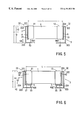
- FIG. 1 is a frontal view of the ceramic capacitor according to the present invention
- FIG. 2 is a frontal sectional view of the ceramic capacitor in FIG. 1;
- FIG. 3 is a partial sectional view illustrating the ceramic capacitor shown in FIGS. 1 and 2 mounted on a circuit board;
- FIG. 4 is an enlarged sectional view illustrating an example of the metal plate terminals that may be employed in the ceramic capacitor according to the present invention
- FIG. 5 is a frontal view illustrating another embodiment of ceramic capacitor according to the present invention.
- FIG. 6 is a frontal view illustrating yet another embodiment of ceramic capacitor according to the present invention.
- FIG. 7 is a perspective illustrating yet another embodiment of the ceramic capacitor according to the present invention.
- FIG. 8 is a frontal view illustrating yet another embodiment of the ceramic capacitor illustrated in FIG. 7;
- FIG. 9 is a perspective illustrating yet another embodiment of the ceramic capacitor according to the present invention.
- FIG. 10 is a frontal view of the ceramic capacitor in FIG. 9;
- FIG. 11 is a frontal view illustrating yet another embodiment of the ceramic capacitor according to the present invention.
- FIG. 12 is a perspective illustrating yet another embodiment of the ceramic capacitor according to the present invention.
- FIG. 13 is a frontal view illustrating yet another embodiment of the ceramic capacitor according to the present invention.
- FIG. 14 is a frontal view illustrating yet another embodiment of the ceramic capacitor according to the present invention.
- FIG. 15 is a frontal view illustrating yet another embodiment of the ceramic capacitor according to the present invention.
- FIG. 16 is a frontal view illustrating yet another embodiment of the ceramic capacitor according to the present invention.
- FIG. 17 is a frontal sectional view illustrating yet another embodiment of the ceramic capacitor according to the present invention.
- FIG. 18 is a frontal sectional view illustrating yet another embodiment of the ceramic capacitor according to the present invention.
- FIG. 19 is a perspective illustrating yet another embodiment of the ceramic capacitor according to the present invention.
- FIG. 20 is a bottom view illustrating yet another embodiment of the ceramic capacitor according to the present invention.
- FIG. 21 is a partial sectional view illustrating an example of the mounted ceramic capacitor shown in FIG. 20;
- FIG. 22 is a frontal view illustrating yet another embodiment of the ceramic capacitor according to the present invention.
- FIG. 23 is a frontal view illustrating yet another embodiment of the ceramic capacitor according to the present invention.
- FIG. 24 is a perspective illustrating yet another embodiment of the ceramic capacitor according to the present invention.
- FIG. 25 is a frontal view illustrating yet another embodiment of the ceramic capacitor illustrated in FIG. 7.
- FIG. 26 is a frontal view illustrating yet another embodiment of the ceramic capacitor according to the present invention.
- the ceramic capacitor according to the present invention includes one ceramic capacitor element 1 and a pair of metal plate terminals 2 and 3 .
- the ceramic capacitor element 1 is provided with terminal electrodes 11 and 12 at the two side end surfaces facing opposite each other in the direction of the length L.
- the ceramic capacitor element 1 is provided with a number of (e.g., 100 layers) internal electrodes 101 and 102 inside a ceramic dielectric base body 100 .
- the internal electrodes 101 are each connected to the terminal electrode 11 at one end, with the other ends constituting free ends, and the internal electrodes 102 are each connected to the terminal electrode 12 at one end with the other ends constituting free ends.
- the materials to constitute the terminal electrodes 11 and 12 , the internal electrodes 101 and 102 and the ceramic dielectric base body 100 , the methods for manufacturing them and the like are of the known art.
- each internal electrode 101 be formed to create a distance ⁇ L 1 between its free end and the terminal electrode 12 .
- Each internal electrode 102 should be formed to create a distance ⁇ L 2 between its free end and the terminal electrode 11 .
- the distances ⁇ L 1 and ⁇ L 2 are minimum distances between the free end and terminal electrode 11 and the free end and the terminal electrode 12 .
- the distance ⁇ L 1 is given as the distance between the line S 11 drawn in the direction of the thickness of the ceramic dielectric base body 100 from the front end of a hanging portion 121 of the terminal electrode 12 deposited onto the front surface and the rear surface of the ceramic dielectric base body 100 and the line S 12 drawn in the direction of the thickness of the ceramic dielectric base body 100 from the front end of the free ends.
- the distance ⁇ L 2 is given as the distance between the line S 21 drawn in the direction of the thickness of the ceramic dielectric base body 100 from the front end of a hanging portion 111 of the terminal electrode 11 deposited onto the front surface and the rear surface of the ceramic dielectric base body 100 and the line S 22 in the direction of the thickness of the ceramic dielectric base body 100 drawn from the front end of the free ends.
- the ceramic capacitor element 1 in FIG. 2 adopts a transverse configuration in which the electrode surfaces of the internal electrodes 101 and 102 extend parallel to the horizontal surface
- a longitudinal configuration achieved by rotating the ceramic capacitor element 1 by approximately 90° from its position in FIG. 2 so that the electrode surfaces of the internal electrodes 101 and 102 extend perpendicular to the horizontal surface may be adopted, instead.
- the metal plate terminal 2 one end 21 of which is connected to the terminal electrode 11 , is provided with a folded portion 22 in the middle area, and a terminal portion 23 to be connected to the outside toward the other end from the folded portion 22 .
- the metal plate terminal 3 one end 31 of which is connected to the terminal electrode 12 , too, is provided with a folded portion 32 in its middle area and a terminal portion 33 to be connected to the outside toward the other end from the folded portion 32 .
- the metal plate terminals 2 and 3 should be constituted of a material having a low electrical resistance and demonstrating outstanding spring property. Typical examples include a phosphor bronze plate. While no particular restriction is imposed on its plate thickness, the plate will be typically 0.1 mm thick.
- the ends 21 and 31 of the metal plate terminals 2 and 3 are respectively connected to the terminal electrodes 11 and 12 via bonding members 4 and 5 .
- FIG. 3 is a partial sectional view illustrating the ceramic capacitor in FIGS. 1 and 2 mounted on a circuit board.
- the ceramic capacitor is mounted on a circuit board 70 , with conductor patterns 71 and 72 formed at the surface of the circuit board 70 .
- the terminal portion 23 of the metal plate terminal 2 provided at the ceramic capacitor is soldered to the conductor pattern 71 with a solder 81
- the terminal portion 33 of the metal plate terminal 3 is soldered to the conductor pattern 72 with a solder 82 .
- the metal plate terminals 2 and 3 are respectively connected to the terminal electrodes 11 and 12 of the ceramic capacitor element 1 at their ends 21 and 31 , and are provided with the folded portions 22 and 32 respectively in their middle areas and the terminal portions 23 and 33 respectively to be connected to the outside toward the other end from the folded portions 22 and 32 .
- the length (height) of the metal plate terminals 2 and 3 structured as described above, extending from the terminal portions to be connected to an external conductor such as a substrate to the ends connected to the terminal electrodes 11 and 12 of the ceramic capacitor element 1 is extended by the folded portions 22 and 32 provided in the middle areas.
- the height from the terminal portions 23 and 33 to the positions at which the metal plate terminals 2 and 3 are connected by using the bonding members 4 and 5 is a component height H
- this height is constituted of the length of the paths h to the apexes of the folded portions 22 and 32 according to the present invention achieving a great increase in height dimension.
- the length of the paths h can be set smaller than the component height H that is allowed in a ceramic capacitor whose entire length is L by adjusting the positions of the apexes of the folded portions 22 and 32 .
- the folded portions 22 and 32 are thus absorbed through the spring effect achieved at the folded portions 22 and 32 to reduce the mechanical stress and the thermal stress occurring at the ceramic capacitor element 1 .
- the distance from the terminal portions 23 and 33 that are mounted at the circuit board 70 to the portions at which the metal electrodes are mounted to the terminal electrodes 11 and 12 of the ceramic capacitor element 1 can be increased by a factor of 2 to 5 compared to the prior art, to prevent cracks from occurring at the ceramic capacitor element 1 .
- the ceramic capacitor is employed as a smoothing capacitor for a switching source that is often mounted at the aluminum circuit board 70 , the occurrence of cracks and the risk of resultant arcing can be avoided.
- the folded portions 22 and 32 provided at the metal plate terminals 2 and 3 , which absorb the flexure and the thermal expansion of the circuit board 70 and prevent an increase in the height.
- the length h of the path over which the spring effect is achieved can be set smaller than the component height H of the ceramic capacitor having the full length L, by adjusting the positions of the apexes of the folded portions 22 and 32 .
- the length h of the path extending from the terminal portions 23 and 33 located toward the circuit board 70 to the ceramic capacitor element mounting portions can be increased for the metal plate terminals 2 and 3 without increasing the component height H, to achieve an improvement in the absorption of the flexure and the thermal expansion of the circuit board 70 by the metal plate terminals 2 and 3 , which, in turn, reduces the mechanical stress and the thermal stress occurring at the ceramic capacitor element 1 .
- the apexes of the folded portions 22 and 32 are set at positions that are lower than the apex of the ceramic capacitor element 1 . Namely, h ⁇ H is satisfied. This structure makes it possible to keep the component height H at a small value.
- the bonding members 4 and 5 for bonding the metal plate terminals 2 and 3 to the terminal electrodes 11 and 12 respectively may be constituted of a conductive adhesive containing resin or of solder.
- the connecting structure whereby the metal plate terminals 2 and 3 are connected to the terminal electrodes 11 and 12 via the bonding members 4 and 5 constituted of a conductive adhesive containing resin hardly any thermal shock is imparted and, consequently, there is no risk of cracks occurring at the ceramic capacitor element 1 before use. This contributes to an improvement in reliability.
- the conductive adhesive contain silver particles as its conductive constituent, since silver particles will improve conductivity.
- Flat silver particles having a particle size of 3 ⁇ m or larger are particularly desirable, as silver particles having such a particle size and shape will achieve an increase in the quantity of silver particles relative to the resin to assure good conductivity.
- the particle size of the silver particles becomes too large, their dispersion in the resin becomes poor, to lower the adhesive strength, it is necessary to determine the maximum particle size of the silver particles to be used by taking into consideration the adhesive strength.
- the resin constituting the conductive adhesive should be a thermosetting resin having a stable temperature resistant property over such a temperature range.
- a thermosetting resin having a stable temperature resistant property over such a temperature range.
- Specific examples of such a resin include epoxy-type thermosetting resin, urethane-type thermosetting resin, polyimide-type thermosetting resin and acrylic-type thermosetting resin.
- electrodes 11 and 12 may be constituted of solder instead of the conductive adhesive described above.
- a solder having a melting point of 200° C. or higher and 400° C. or lower is particularly suited for this application.
- the soldering process is implemented at a temperature of approximately 200° C.
- the bonding members 4 and 5 connecting the metal plate terminals 2 and 3 to the terminal electrodes 11 and 12 must not become fused.
- solder having a melting point of 400° C. or higher is used to constitute the bonding members 4 and 5 , heat exceeding 400° C. will be applied to the ceramic capacitor element 1 while soldering the metal plate terminals 2 and 3 to the terminal electrodes 11 and 12 , to form thermal cracks at the ceramic capacitor element 1 .
- the solder must have a melting point of 400° C. or lower.
- the metal plate terminals 2 and 3 be provided with a cover film having a non-adhesive property with respect to the solder at, at least, surfaces facing opposite the external connection surfaces of the terminal portions 23 and 33 . This aspect is now explained in reference to FIG. 4 .
- a substrate 200 is formed from a plate material constituted of phosphor bronze, iron-nickel alloy or the like and a metal film 201 that achieves good soldering is provided on the side where the external connection surface that is connected to the outside through soldering (the outer side) is present, with a cover film 202 to which the solder does not adhere or adheres less readily is laminated at the inside on the opposite side. Since the use of such metal plate terminals 2 and 3 ensures that the solder does not adhere to the surfaces of the terminal portions 23 and 33 as illustrated in FIG. 3, the areas between the terminal portions 23 and 33 and the terminal portions 23 and 33 are not filled with the solder. Thus, the spring property of the metal plate terminals 2 and 3 is not compromised.
- the cover film 202 may be laminated over the entire lengths of the metal plate terminals 2 and 3 , or may be partially laminated including the terminal portions 23 and 33 .
- the cover film 202 may be constituted of one of the following: a metal oxide film, wax, resin and silicon oil.
- a metal oxide film As a means for forming the metal oxide film, a method whereby a metal film such as Ni or Cu, which readily becomes oxidized is laminated at the surface of the substrate 200 through plating and is left in a natural state to become oxidized may be employed.
- the metal film 201 may be constituted as an Sn or Pb—Sn plated film.
- the terminal portions 23 and 33 are provided under the ceramic capacitor element 1 over a distance. This structure prevents an increase in the area occupied by the terminal portions 23 and 33 at the substrate to achieve a capacitor with a minimum mounting area.
- the folded portion 22 of the metal plate terminal 2 includes a first bent portion 221 and a second bent portion 222 .
- the folded portion 22 is bent to fold away from the terminal electrode 11 at the first bent portion 221 , whereas at the second bent portion 222 , it is bent to extend in a direction parallel to the end surface over a distance from the first bent portion 221 .
- the metal plate terminal 2 is connected to the terminal electrode 11 at the area extending from its front end to the first bent portion 221 .
- the folded portion 32 of the metal plate terminal 3 includes a first bent portion 321 and a second bent portion 322 .
- the folded portion 32 is bent to fold in a direction that moves away from the terminal electrode 12 at the first bent portion 321 , whereas at the second bent portion 322 it is bent to extend in a direction parallel to the end surface over a distance from the first bent portion 321 .
- the metal plate terminal 3 is connected to the terminal electrode 12 at the area extending from its front end to the first bent portion 321 .
- the structure described above achieves a spring effect in the areas extending from the first bent portions 221 and 321 and the second bent portions 222 and 322 to the terminal portions 23 and 33 so that the flexure and the thermal expansion of the substrate can be absorbed through the spring effect.
- the metal plate terminal 2 is provided with a third bent portion 223 .
- the third bent portion 223 partitions the folded portion 22 from the terminal portion 23 .
- the metal plate terminal 3 is provided with a third bent portion 323 .
- the third bent portion 323 partitions the folded portion 32 from the terminal portion 33 .
- the metal plate terminals 2 and 3 are bent at the third bent portions 223 and 323 respectively in a direction in which their terminal portions 23 and 33 are placed closer to the ceramic capacitor element 1 .
- the terminal portions 23 and 33 of the metal plate terminals 2 and 3 are provided under the ceramic capacitor element 1 over distances G 01 and G 02 respectively to minimize the mounting area by preventing an increase in the area occupied by the terminal portions 23 and 33 at the substrate.
- the internal electrodes 101 and the internal electrodes 102 do not overlap each other at the interfaces of the metal plate terminals and the conductive adhesive where cracks and damage tend to occur readily, and near the areas where the conductive adhesive is applied.
- the risks of shorting caused by cracks and of arcing resulting from shorting are drastically reduced.
- first bent portions 221 and 321 and the second bent portions 222 and 322 are bent at an angle of approximately 90° in FIGS. 1 and 2, they may be bent at angles other than 90°. Furthermore, the first bent portions 221 and 321 and the second bent portions 222 and 322 may be bent in a shape without a clear angle, e.g., in an arc shape, instead.
- FIG. 5 is a frontal view illustrating another embodiment of the ceramic capacitor according to the present invention.
- the same reference numbers are assigned to components identical to those in FIGS. 1 and 2 to preclude the necessity for repeated explanation thereof.
- the bonding members 4 and 5 containing resin are partially deposited onto the terminal electrodes 11 and 12 .
- the length h of the path extending from the terminal portions 23 and 33 toward the substrate to the ceramic capacitor element mounting portions can be increased for the metal plate terminals 2 and 3 without increasing the component height H to improve the effect for absorbing the flexure and the thermal expansion of the substrate.
- FIG. 6 is a frontal view illustrating another embodiment of the ceramic capacitor according to the present invention.
- the same reference numbers are assigned to components identical to those in FIGS. 1 and 2 to preclude the necessity for repeated explanation thereof.
- the metal plate terminal 2 is provided with another bent portion 224 in the area extending from its front end to the first bent portion 221 , with the portion extending from the other bent portion 224 to the first bent portion 221 facing opposite a side end surface of the ceramic capacitor element 1 over a distance G 1 and the area between the front end and the other bent portion 224 connected to the terminal electrode 11 .
- the metal plate terminal 3 is provided with another bent portion 324 in the area extending from its front end to the first bent portion 321 , with the portion extending from the other bent portion 324 to the first bent portion 321 facing opposite the side end surface over a distance G 2 and the area between the front end and the other bent portion 324 connected to the terminal electrode 12 .
- the length over which the spring effect is achieved is increased to further improve the effect for absorbing the flexure and the thermal expansion of the substrate.
- the length h of the paths extending from the terminal portions 23 and 33 located toward the substrate to the ceramic capacitor element mounting portions can be increased without having to increase the component height H, for the metal plate terminals 2 and 3 , to improve the absorption effect through which the flexure and the thermal expansion of the substrate are absorbed.
- FIG. 7 is a perspective illustrating yet another embodiment of ceramic capacitor according to the present invention and FIG. 8 is a frontal view of the ceramic capacitor in FIG. 7 .
- the ceramic capacitor in this embodiment is provided with two ceramic capacitor elements 110 and 120 .
- the ceramic capacitor elements 110 and 120 are laminated sequentially, with the terminal electrodes 11 and 12 connected in parallel via the bonding members 4 and 5 .
- the terminal portions 23 and 33 of the metal plate terminals 2 and 3 are provided under the ceramic capacitor element 120 located at the lowermost layer of the ceramic capacitor elements 110 and 120 , over distances G 01 and G 02 respectively to minimize the mounting area by preventing an increase in the area occupied by the terminal portions 23 and 33 at the substrate.
- the folded portions 22 and 32 of the metal plate terminals 2 and 3 include the first bent portions 221 and 321 and the second bent portions 222 and 322 respectively. They are bent away from the terminal electrodes 11 and 12 at the first bent portions 221 and 321 , whereas they are bent at the second bent portions 222 and 322 in a direction extending parallel to the side end surfaces of the ceramic capacitor elements 110 and 120 over distances from the first bent portions 221 and 321 respectively.
- the portions of the metal plate terminals 2 and 3 extending from their front ends to the first bent portions 221 and 321 are connected to the terminal electrodes 11 and 12 formed at the side end surfaces of the ceramic capacitor elements 110 and 120 .
- the bonding members 4 and 5 constituted of solder or a conductive adhesive containing resin are employed to connect the metal plate terminals 2 and 3 to the terminal electrodes 11 and 12 and to connect the ceramic capacitor elements 110 and 120 to each other.
- FIG. 9 is a perspective illustrating yet another embodiment of the ceramic capacitor according to the present invention and FIG. 10 is a frontal view of the ceramic capacitor in FIG. 9 .
- the same reference numbers are assigned to components identical to those in FIGS. 7 and 8.
- the metal plate terminals 2 and 3 are only connected to the terminal electrodes 11 and 12 formed at the side end surfaces of the ceramic capacitor element 120 at the areas extending from their front ends to the first bent portions 221 and 321 .
- This embodiment achieves advantages similar to those achieved in the embodiment illustrated in FIGS. 7 and 8.
- FIG. 11 is a frontal view illustrating yet another embodiment of the ceramic capacitor according to the present invention.
- the same reference numbers are assigned to components identical to those in FIGS. 7 to 10 .
- the metal plate terminals 2 and 3 are only connected to the terminal electrodes 11 and 12 formed at the side end surfaces of the ceramic capacitor element 120 at the areas extending from their front ends to the first bent portions 221 and 321 .
- FIG. 12 is a perspective illustrating yet another embodiment of the ceramic capacitor according to the present invention.
- the metal plate terminals 2 and 3 are respectively provided with notched portions 225 and 325 in the middle areas of the folded portions 22 and 32 in the widthwise direction. The presence of these notched portions 225 and 325 reduces heat conduction occurring from the metal plate terminals 2 and 3 toward the ceramic capacitor elements 110 and 120 to lessen the thermal stress at the ceramic capacitor elements 110 and 120 .
- the rigidity of the metal plate terminals 2 and 3 is reduced, a spring effect that is suited for absorbing the flexure and the thermal expansion of the substrate is achieved.
- FIG. 13 is a frontal view illustrating yet another embodiment of the ceramic capacitor according to the present invention.
- the same reference numbers are assigned to components identical to those in FIGS. 8 to 12 .
- the metal plate terminals 2 and 3 are connected only to the terminal electrodes 11 and 12 formed at the side end surfaces of the ceramic capacitor element 110 at the areas extending from their front ends to the first bent portions 221 and 321 .
- the length h of the paths over which the spring effect is achieved is the length of the areas extending from the terminal portions 23 and 33 to the second bent portions 222 and 322 .
- the length extending to the positions at which the metal plate terminals 2 and 3 are connected via the bonding members 4 and 5 is the length h of the paths that is larger than the height h 0 (see FIG. 1 and the like) in the prior art without the folded portions 22 and 32 .
- the absorption effect for absorbing the flexure and the thermal expansion of the substrate is improved to reduce the mechanical stress and thermal stress occurring at the ceramic capacitor elements 110 and 120 .
- FIG. 14 is a frontal view illustrating yet another embodiment of the ceramic capacitor according to the present invention.
- the metal plate terminals 2 and 3 are respectively provided with other bent portions 224 and 324 at the areas extending from the front ends to the first bent portions 221 and 321 , with the portions extending from the other bent portions 224 and 324 to the first bent portions 221 and 321 facing opposite the side end surfaces of the ceramic capacitor elements 110 and 120 over distances G 1 and G 2 and the areas between the front ends and the other bent portions 224 and 324 connected to the terminal electrodes 11 and 12 .
- the portion between its front end and the other bent portion 224 is located between the terminal electrode 11 of the ceramic capacitor element 110 and the terminal electrode 11 of the ceramic capacitor element 120 and is connected and secured to the terminal electrodes 11 and 11 via the bonding member 4 constituted of solder or a conductive adhesive containing resin.
- the portion between its front end and the other bent portion 324 is located between the terminal electrode 12 of the ceramic capacitor element 110 and the terminal electrode 12 of the ceramic capacitor element 120 and is connected and secured to the terminal electrodes 12 and 12 via the bonding member 5 constituted of solder or a conductive adhesive containing resin.
- FIG. 15 is a frontal view illustrating yet another embodiment of the ceramic capacitor according to the present invention.
- the portion between the front end and the other bent portion 224 at the metal plate terminal 2 is located so that it receives the terminal electrode 11 of the ceramic capacitor element 120 at the lowermost layer and is connected and secured to the terminal electrode 11 by the bonding member 41 constituted of solder or a conductive adhesive containing resin.
- the portion between the front end and the other bent portion 324 at the metal plate terminal 3 is located so that it receives the terminal electrode 12 of the ceramic capacitor element 120 at the lowermost layer and is connected and secured to the terminal electrode 12 by the bonding member 51 constituted of solder or a conductive adhesive containing resin.
- FIG. 16 is a frontal view illustrating yet another embodiment of the ceramic capacitor according to the present invention.
- four ceramic capacitor elements 110 to 140 are sequentially laminated, with the areas between the terminal electrodes 11 — 11 and the areas between the terminal electrodes 12 — 12 bonded with the bonding members 41 to 43 and 51 to 53 constituted of solder or a conductive adhesive containing resin.
- the portion between its front end and the first bent portion 221 is connected and secured to the terminal electrode 11 by the bonding member 41 constituted of solder or a conductive adhesive containing resin.
- the portion between its front end and the first bent portion 321 is connected and secured to the terminal electrode 12 by the bonding member 51 constituted of solder or a conductive adhesive containing resin.
- the embodiment illustrated in FIG. 16 achieves an even greater capacitance than those achieved in the embodiments illustrated in FIGS. 1 to 15 .
- the number of ceramic capacitor elements 110 to 140 may be increased further to achieve the desired capacitance.
- FIG. 17 is a frontal sectional view illustrating yet another embodiment of the ceramic capacitor according to the present invention.
- the same reference numbers are assigned to components identical to those in FIGS. 1 and 2 and their explanation is omitted.
- the terminal electrodes 11 and 12 are formed only at the side end surfaces. Since this structure allows the distance ⁇ L 1 between the internal electrodes 101 and the terminal electrode 12 and the distance ⁇ L 2 between the internal electrodes 102 and the terminal electrode 11 to be set in reference to the side end surfaces of the ceramic dielectric base body 100 , the area over which the internal electrodes 101 and the internal electrodes 102 overlap each other can be increased to assure an even larger capacity.
- FIG. 18 is a frontal sectional view illustrating yet another embodiment of the ceramic capacitor according to the present invention.
- the same reference numbers are assigned to components identical to those in FIG. 17 and their explanation is omitted.
- two ceramic capacitor elements 110 and 120 are provided.
- the ceramic capacitor elements 110 and 120 are laminated sequentially, with the terminal electrodes 11 and 12 connected in parallel via the bonding members 4 and 5 .
- the terminal electrodes 11 and 12 are formed only at the side end surfaces of the ceramic dielectric base body 100 .
- FIG. 19 is a perspective illustrating yet another embodiment of the ceramic capacitor according to the present invention.
- the metal plate terminal 2 is provided with a punched portion 24 .
- the punched portion faces opposite the mounting portion at which the terminal electrode 11 is mounted.
- the metal plate terminal 3 is provided with a punched portion 34 .
- the punched portion 34 faces opposite the mounting portion at which the terminal electrode 12 is mounted.
- connection work for connecting the metal plate terminals 2 and 3 to the terminal electrodes 11 and 12 allows the connection work for connecting the metal plate terminals 2 and 3 to the terminal electrodes 11 and 12 to be carried out with ease by holding the mounting portions of the metal plate terminals 2 and 3 through the punched portions 24 and 34 of the metal plate terminals 2 and 3 respectively to place them in contact with the terminal electrode 11 and 12 .
- the mounting portions can be bonded to the terminal electrodes 11 and 12 with a uniform force.
- FIG. 20 is a bottom view illustrating yet another embodiment of the ceramic capacitor according to the present invention.
- the same reference numbers are assigned to components identical to those in FIGS. 1 and 2 to preclude the necessity for repeated explanation thereof.
- the terminal portion 23 of the metal plate terminal 2 is provided with two holes 231 and 232 .
- the terminal portion 33 of the metal plate terminal 3 is provided with two holes 331 and 332 .
- the quantities of holes at the terminal portions are arbitrary.
- FIG. 21 is a partial sectional view illustrating the ceramic capacitor shown in FIG. 20 mounted at the circuit board 70 .
- solders 821 and 811 are charged to fill the holes 231 and 232 and the holes 331 and 332 at the terminal portions 23 and 33 respectively to solder the ceramic capacitor onto the circuit board 70 with a high degree of reliability.
- FIG. 22 is a frontal view illustrating yet another embodiment of the ceramic capacitor according to the present invention.
- the same reference numbers are assigned to components identical to those in FIGS. 1 and 2 to preclude the necessity for repeated explanation thereof.
- the folded portion 22 of the metal plate terminal 2 includes an acute angle bent portion 221 at which the folded portion 22 is bent to fold at an acute angle in a direction such that it faces roughly opposite the end surface of the ceramic capacitor element 1 .
- the folded portion 32 of the metal plate terminal 3 includes an acute-angle bent portion 321 at which the folded portion 32 is bent at an acute angle in a direction such that it faces roughly opposite the end surface of the ceramic capacitor element 1 .
- a spring effect is achieved in the areas extending from the bending positions 221 and 321 to the terminal portions 23 and 33 , as in the ceramic capacitor illustrated in FIGS. 1 and 2, so that the flexure and the thermal expansion of the substrate are absorbed through the spring effect.
- the maximum distance d between the two portions facing opposite each other formed by the bending at each the metal plate terminals 2 and 3 be set at 300 ⁇ m or less.
- Table I presents test data indicating the crack occurrence rate (%), obtained by performing excitation for two hours at frequencies ranging from 10 Hz to 500 Hz while varying the distance d in ceramic capacitors structured as illustrated in FIG. 22 .
- the quantity of ceramic capacitors that were tested for individual distances d was 100.
- the crack occurrence rate reaches 85% to 100% when the distance d is at 370 ⁇ m or more, well above 300 ⁇ m. In contrast, when the distance d ( ⁇ m) is at or less than 300 ⁇ m, i.e., at 70 ⁇ m and 90 ⁇ m, no cracks occur.
- FIG. 23 is a frontal view illustrating yet another embodiment of the ceramic capacitor according to the present invention.
- the same reference numbers are assigned to components identical to those in FIGS. 1 and 2 to preclude the necessity for repeated explanation thereof.
- the folded portions 22 and 32 on the metal plate terminals 2 and 3 are bent in an arc. In this embodiment, too, advantages similar to those achieved in the embodiment illustrated in FIGS. 1 and 2 are achieved.
- FIGS. 3 to 21 may be adopted when employing the metal plate terminals 2 and 3 shown in FIGS. 22 and 23.
- FIGS. 22 and 23 it goes without saying that there are a number of ways in which the embodiments may be combined.
- the ceramic capacitor elements described above were each provided with internal electrodes constituted of Ag—Pd inside a ceramic dielectric body constituted of lead-type complex perovskite and terminal electrodes constituted of baked electrodes formed from an Ag paste containing glass frit at the two side end surfaces of the ceramic dielectric body facing opposite each other.
- a ceramic capacitor was prepared by employing the means for producing embodiments 1 to 4 without using any metal plate terminals.
- Table II presents the states of crack occurrence manifesting in embodiments 1 to 4 and comparison examples 1 and 2 after a heat cycle test.
- the ceramic capacitor elements described above were each provided with internal electrodes constituted of Ag—Pd embedded in a ceramic dielectric body constituted of lead-type complex perovskite and terminal electrodes constituted of baked electrodes formed from an Ag paste containing glass frit at the two side end surfaces of the ceramic dielectric body facing opposite each other.
- the metal plate terminals were mounted by adopting the structure and the positional arrangement illustrated in FIG. 16.
- a metal plate (phosphor bronze) having a thickness of 0.1 mm that had undergone a silver plating treatment (the middle layer was constituted of nickel, Ni—Ag) was used to constitute the metal plate terminals.
- the terminal portions located at the front ends of the metal plate terminals were pressed onto the side surfaces of the terminal electrodes of the ceramic capacitor element located at the lowermost layer among the ceramic capacitor elements that had been stacked over four levels, with a specific pressure. In this state, heat was applied at 150° C. for 1 hour to thermally harden the conductive adhesive to prepare a combined ceramic capacitor having the four ceramic capacitor elements and the metal plate terminals bonded at the terminal electrodes.
- test pieces prepared through the process described above were embodiments 5 to 7.
- a ceramic capacitor was prepared by employing the means for producing embodiments 5 to 7 without using any metal plate terminals.
- Table III presents the states of crack occurrence manifesting in embodiments 5 to 7 and comparison examples 3 and 4 after a heat cycle test.
- Ceramic capacitor elements with dimensions of 5.6 mm ⁇ 5.0 mm ⁇ 2.3 mm and having a capacitance of 22 ⁇ F., temperature characteristics E and a rated voltage of 25V were prepared.
- the ceramic capacitor elements described above were each provided with internal electrodes constituted of Ag—Pd embedded in a ceramic dielectric body constituted of lead-type complex perovskite and terminal electrodes constituted of baked electrodes formed from an Ag paste containing glass frit at the two side end surfaces facing opposite each other.
- the metal plate terminals were mounted by adopting the structure and the positional arrangement illustrated in FIG. 16.
- a metal plate (phosphor bronze) having a thickness of 0.1 mm that had undergone a silver plating treatment (the middle layer was constituted of nickel, Ni—Ag) was used to constitute the metal plate terminals.
- the terminal portions located at the front ends of the metal plate terminals were pressed onto the side surfaces of the terminal electrodes of the ceramic capacitor element located at the lowermost layer among the ceramic capacitor elements that had been stacked over four levels, with a specific pressure. In this state, heat was applied at 150° C. for 1 hour to thermally harden the conductive adhesive to prepare a combined ceramic capacitor having the four ceramic capacitor elements and the metal plate terminals bonded at the terminal electrodes.
- Ceramic capacitor elements with dimensions of 5.6 mm ⁇ 5.0 mm ⁇ 2.3 mm and having a capacitance of 22 ⁇ F., temperature characteristics E and a rated voltage of 25V were prepared.
- the ceramic capacitor elements described above were each provided with internal electrodes constituted of Ag—Pd inside a ceramic dielectric body constituted of lead-type complex perovskite and terminal electrodes constituted of baked electrodes formed from an Ag paste containing glass frit at the two side end surfaces of the ceramic dielectric body facing opposite each other.
- Ceramic capacitor elements with dimensions of 3.2 mm ⁇ 2.5 mm ⁇ 1.0 mm and having a capacitance of 6.8 ⁇ F., temperature characteristics E and a rated voltage of 16V were prepared.
- the ceramic capacitor elements described above were each provided with internal electrodes constituted of Ag—Pd inside a ceramic dielectric body constituted of lead-type complex perovskite and terminal electrodes constituted of baked electrodes formed from an Ag paste containing glass frit.
- the metal plate terminals were constituted of a metal plate (phosphor bronze) having a thickness of 0.1 mm that had undergone a plating treatment.
- test pieces obtained through the methods explained in reference to embodiment 8 and comparison examples 5 and 6 were placed in a thermal shock test tank with the terminal portions of its metal plate terminals soldered onto an aluminum substrate to undergo thermal shock testing.
- the thermal shock test was conducted for 40 cycles and 100 cycles with the temperature changing from 125° C. to ⁇ 55° C. to 125° C. in a cycle.
- the test pieces were inspected to ascertain the presence/absence of cracks inside the ceramic capacitor elements before and after testing.
- the metal plate terminals 2 and 3 are each constituted of a metal material having a coefficient of average linear expansion ⁇ of 13 ⁇ 10 ⁇ 6 or less over a temperature range of ⁇ 50° C. to 125° C.
- a metal material having a coefficient of average linear expansion ⁇ of 13 ⁇ 10 ⁇ 6 or less over a temperature range of ⁇ 50° C. to 125° C.
- Specific examples of such a metal material include an Fe—Ni alloy with an Fe content of 55 wt % to 70 wt % and an Ni content of 35 wt % to 45 wt %.
- any of the following metal materials may be employed to constitute the metal plate terminals 2 and 3 in the ceramic capacitor according to the present invention.
- the metal plate terminals are constituted by using any of the metal materials having the coefficients of average linear expansion ⁇ listed above, no cracks occur and the risk of arcing is thus eliminated as well even if the ceramic capacitor is continuously operated over an extended period of time in an environment in which the temperature changes drastically within the range of ⁇ 55° C. to 125° C. Consequently, when it is employed as a smoothing capacitor at a switching source that is turned on/off frequently to result in a temperature fluctuation within the range of ⁇ 55° C. to 125° C., a sufficient degree of reliability is assured.
- the metal plate terminals 2 and 3 each realizing a coefficient of average linear expansion ⁇ of 13 ⁇ 10 ⁇ 6 or less over the temperature range of ⁇ 55° C. to 125° C.
- a ceramic capacitor that is free of cracks and also free of risk of arcing even when it is continuously operated over an extended period of time in an environment where the temperature changes drastically over the range of ⁇ 55° C. to 125° C. is achieved.
- Ceramic capacitor elements with dimensions of 5.6 mm ⁇ 5.0 mm ⁇ 2.3 mm and having a capacitance of 22 ⁇ F., temperature characteristics E and a rated voltage of 25V were prepared.
- the ceramic capacitor elements described above were each provided with internal electrodes constituted of Ag—Pd inside a ceramic dielectric body constituted of lead-type complex perovskite and terminal electrodes constituted of baked electrodes formed from an Ag paste containing glass frit at the two side end surfaces of the ceramic dielectric body facing opposite each other.
- FIG. 24 is a perspective of a ceramic capacitor obtained through the process described above and FIG. 25 is a frontal view of the ceramic capacitor illustrated in FIG. 24 .
- the metal plate terminals 2 and 3 were constituted by using different metal materials having a coefficient of average linear expansion at 13 ⁇ 10 ⁇ 6 or lower.
- the metal plate terminals 2 and 3 were constituted of Inconel X-750 (embodiment 11), in embodiment 12 they were constituted of Nimonic 90, in embodiment 13 they were constituted of carbon steel, in embodiment 14 they were constituted of stainless 430, in embodiment 15 they were constituted of Hasteroy B, in embodiment 16 they were constituted of stainless steel 403, in embodiment 17 they were constituted of pure titanium, in embodiment 18 they were constituted of industrial titanium, in embodiment 19 they were constituted of chromium, in embodiment 20 they were constituted of 42 Alloy and in embodiment 21 they were constituted of Invar.
- the ceramic capacitors in embodiments 11 to 21 were each secured to an aluminum substrate through soldering, and were subjected to thermal shock to evaluate occurrence of cracks.
- the thermal shock was applied under the following conditions.
- Embodiments 11 to 21 each underwent 400 heat cycles.
- ceramic capacitors as illustrated in FIGS. 24 and 25 were manufactured by using metal materials each having a coefficient of average linear expansion exceeding 13 ⁇ 10 ⁇ 6 to constitute the metal plate terminals 2 and 3 .
- the metal plate terminals 2 and 3 were constituted of aluminum, in comparison example 12, they were constituted of iron, in comparison example 13, they were constituted of silver, in comparison example 14, they were constituted of phosphor bronze, in comparison example 15, they were constituted of stainless steel 304, in comparison example 16, they were constituted of copper, in comparison example 17, they were constituted of nickel silver, in comparison example 18, they were constituted of stainless steel 317 and in comparison example 19, they were constituted of nickel.
- the ceramic capacitors in comparison examples 11 to 19 were each secured onto an aluminum substrate through soldering to evaluate occurrence of cracks by applying thermal shock.
- the thermal shock was applied under conditions identical to those for embodiments 11 to 20.
- Table IV presents occurrence of cracks observed after the heat cycles in embodiments 11 to 21 and comparison examples 11 to 19.
- the ceramic capacitor elements described above were each provided with internal electrodes constituted of Ag—Pd inside a ceramic dielectric body constituted of lead-type complex perovskite and terminal electrodes constituted of baked electrodes formed from an Ag paste containing glass frit at the two side end surfaces of the ceramic dielectric body facing opposite each other.
- the metal plate terminals 2 and 3 prepared by varying the material composition of an Fe—Ni alloy, were used.
- the metal plate terminals 2 and 3 were constituted of an Fe—Ni alloy having a composition of Fe 55%—Ni 45%.
- the ceramic capacitors in embodiments 22 to 25 were each secured to an aluminum substrate through soldering and were subjected to thermal shock to evaluate occurrence of cracks.
- the thermal shock was applied under the conditions described earlier in reference to embodiments 11 to 21.
- ceramic capacitors in comparison examples 20 and 21 constituted by forming the metal plate terminals 2 and 3 with Fe—Ni alloys having different material compositions were prepared.
- the metal plate terminals 2 and 3 were constituted of an Fe—Ni alloy having a material composition of Fe 50%—Ni 50% and in comparison example 21, they were constituted of an Fe—Ni alloy having a material composition of Fe 75%—Ni 25%.
- the ceramic capacitors in the comparison examples were prepared through a process that is otherwise similar to that adopted to prepare embodiments 22 to 25.
- the ceramic capacitors in comparison examples 20 and 21 were each secured to an aluminum substrate through soldering and subjected to thermal shock to evaluate occurrence of cracks.
- the thermal shock was applied under conditions described earlier in reference to embodiments 11 to 21.
- Table V presents occurrence of cracks observed in embodiments 22 to 25 and comparison examples 20 and 21 after heat cycles.
- the ceramic capacitor element 1 must satisfy ⁇ 1 ⁇ 2 with ⁇ 1 representing the coefficient of average linear expansion over a temperature range of 25° C. to ⁇ 55° C. and ⁇ 2 representing the coefficient of average linear expansion within a range of 25° C. to 125° C.
- the metal plate terminal 2 is connected to the terminal electrode 11 and the metal plate terminal 3 is connected to the terminal electrode 12 .
- the metal plate terminals 2 and 3 must satisfy ⁇ 1.3 ⁇ 2 and ⁇ >0.7 ⁇ 1 with ⁇ representing their coefficient of average linear expansion within a range of ⁇ 55° C. to 125° C.
- the ceramic capacitor element 1 expands to a larger degree than the metal plate terminals 2 and 3 over the temperature range of 25° C. to 125° C., resulting in a compressive stress occurring at the ceramic capacitor element 1 .
- the individual coefficients are set to satisfy ⁇ 2 , no cracks occur at the ceramic capacitor element 1 over the temperature range of 25° C. to 125° C.
- the ceramic capacitor element 1 expands to a lesser degree than the metal plate terminals 2 and 3 over the temperature range of 25° C. to 125° C., resulting in tensile stress occurring at the ceramic capacitor element 1 .
- ⁇ 1.3 ⁇ 2 in this case, no cracks occur even if tensile stress occurs at the ceramic capacitor element 1 since the stress is insignificant.
- both the ceramic capacitor element 1 and the metal plate terminals 2 and 3 tend to contract proportionally with the temperature relative to 25° C.
- ⁇ 1 since the ceramic capacitor element 1 contracts to a lesser degree than the contraction of the metal plate terminals 2 and 3 , compressive stress occurs at the ceramic capacitor element 1 . As a result, no cracks occur at the ceramic capacitor element 1 .
- the ceramic capacitor element 1 contracts to a greater degree than the metal plate terminals 2 and 3 over the temperature range of ⁇ 55° C. to 25° C. resulting in tensile stress occurring at the ceramic capacitor element 1 .
- 0.7 ⁇ 1 ⁇ in this case, no cracks occur even if tensile stress occurs at the ceramic capacitor element 1 since the stress is low.
- the ceramic capacitor element 1 satisfies ⁇ 1 ⁇ 7 ⁇ 10 ⁇ 6 and ⁇ 2 ⁇ 9 ⁇ 10 ⁇ 6 .
- the main constituent of the dielectric base body 100 is lead-type complex perovskite, ⁇ 1 ⁇ 2 ⁇ 10 ⁇ 6 and ⁇ 2 ⁇ 3 ⁇ 10 ⁇ 6 are satisfied.
- a typical example of the lead-type complex perovskite (relaxor) ceramic dielectric material that may be employed in the present invention is a substance expressed with a composition formula Pb(Mg 1/3 Nb 2/3 )O 3 —Pb(Mg 1/2 W 1/2 )O 3 —PbTiO 3 .
- This composition formula is normally expressed as PMN—PMW—PT.
- substances expressed through regularized formulae such as PMN—Pnn—PT, PMN—PZt—PT and PMN—Pnn—PMW—PT may be used as well.
- the coefficients of average linear expansion ⁇ of the metal plate terminals 2 and 3 all satisfy ⁇ 1.3 ⁇ 2 and ⁇ >0.7 ⁇ 1 over the temperature range of ⁇ 55° C. to 125° C.
- ceramic capacitors that do not form any cracks and do not present the risk of arcing even when they are continuously operated over an extended period of time in an environment in which the temperature changes drastically over the range of ⁇ 55° C. to 125° C. are achieved.
- a lead-type dielectric body with dimensions of 5.6 mm ⁇ 5.0 mm ⁇ 2.3 mm and achieving a capacitance of 22 ⁇ F. and temperature characteristics E at a rated voltage of 25V was prepared to constitute a ceramic capacitor element.
- the ceramic capacitor element was provided with internal electrodes constituted of Ag—Pd inside the lead-type ceramic dielectric body and terminal electrodes constituted of baked electrodes that were formed from an Ag paste containing glass frit at the two side end surfaces of the ceramic dielectric body facing opposite each other.
- the coefficient of average linear expansion ⁇ 1 of the lead-type ceramic capacitor element over the temperature range of ⁇ 55° C. to 25° C. was 0.5 to 2 ⁇ 10 ⁇ 6 and its coefficient of average linear expansion ⁇ 2 over the temperature range of 25° C. to 125° C. was 4.2 ⁇ 10 ⁇ 6 .
- Samples of embodiments 31 to 33 were obtained by using metal materials having different coefficients of average linear expansion to constitute the metal plate terminals 2 and 3 .
- the metal plate terminals 2 and 3 were constituted of chromium
- in embodiment 32 they were constituted of 42 Alloy (Fe 58 wt %—Ni 42 wt %) and in embodiment 33 they were constituted of Invar.
- the coefficient of average linear expansion ⁇ of the chromium used in embodiment 31 is 4.5 ⁇ 10 ⁇ 6 and the coefficient of average linear expansion ⁇ of the 42 Alloy used in embodiment 32 is 4.4 ⁇ 10 ⁇ 6 . Consequently, 0.7 ⁇ 1 ⁇ and to the ⁇ 1.3 ⁇ 2 are satisfied in embodiments 31, 32 and 33.
- Ceramic capacitors in comparison examples 31 to 45 were prepared by using materials different from those used in the embodiments to constitute the metal plate terminals 2 and 3 through the process described in reference to embodiments 31 to 33.
- the materials used in comparison examples 31 to 45 to constitute their metal plate terminals 2 and 3 and their coefficients of average linear expansion ⁇ are listed in Table VI.
- Samples of embodiments 31, 32 and 33 and comparison examples 31 to 45 were each secured onto an aluminum substrate through soldering and were subjected to thermal shock to evaluate occurrence of cracks.
- Table VI presents occurrence of cracks observed in embodiments 31 to 33 and comparison examples 31 to 45 after the heat cycles.
- the materials constituting the metal plate terminals 2 and 3 and the coefficients of average linear thermal expansion ⁇ of the metal plate terminals 2 and 3 employed in embodiments 51 to 59 are as indicated in Table VII, all satisfying 0.7 ⁇ 1 ⁇ and ⁇ 1.3 ⁇ 2 .
- the ceramic capacitors in comparison examples 51 to 59 were prepared in the process identical to that through which the embodiments 51 to 59 were prepared except that the materials to constitute the metal plate terminals 2 and 3 were varied.
- the materials constituting the metal plate terminals 2 and 3 and their coefficients of average linear expansion ⁇ in comparison examples 51 to 59 are listed in Table VII. In none of the comparison examples is 0.7 ⁇ 1 ⁇ or ⁇ 1.3 ⁇ 2 satisfied except for comparison example 59, in which 0.7 ⁇ 1 ⁇ is satisfied and ⁇ 1.3 ⁇ 2 is not satisfied.
- Ceramic capacitor elements having internal electrodes whose main constituent was Ni were adopted in embodiments 31 to 33 and 51 to 59 to conduct a comparative examination of occurrence of cracks. The results of the examination demonstrate almost no significant difference for all of the embodiments, i.e., embodiments 31 to 33 and 51 to 59.
- a ceramic capacitor achieving a high degree of corrosion resistance that does not change much over time is inexpensive and achieves a high degree of reliability.
- FIG. 26 illustrates a combined ceramic capacitor constituted by combining a plurality of ceramic capacitor elements 110 to 150 .
- the same reference numbers are assigned to components identical to those included in the previous drawings.
- the shapes and external dimensions of the plurality of ceramic capacitor elements 110 to 150 are almost the same, with each ceramic capacitor element provided with terminal electrodes 11 and 12 at the two ends facing opposite each other.
- the plurality of ceramic capacitor elements 110 to 150 are combined with their terminal electrodes 11 aligned with one another and their terminal electrodes 12 aligned with one another to constitute a capacitor assembly.
- the metal plate terminals 2 and 3 are secured onto the terminal electrodes 11 and 12 provided at the two ends of the capacitor assembly via solders 4 and 5 respectively.
- solder particles contained in the solder paste have a particle size of 35 ⁇ m to 55 ⁇ m and only a small portion of the flux component is contained in the solder paste, the solder particles are effectively prevented from entering the gaps between the electrodes.
- no activator constituted of a halogen compound of chlorine, bromine or the like is contained, any degradation of the insulation resistance is prevented as well.
- the ceramic capacitor elements 110 to 150 are assembled by maintaining gaps g formed between them within a range of approximately 10 ⁇ m to 20 ⁇ m.
- the gaps g may be set at 20 ⁇ m or less by combining the ceramic capacitor elements 110 to 150 provided with the terminal electrodes 11 and 12 whose thickness is set at 20 ⁇ m or less.
- the metal plate terminals 2 and 3 are mounted to the two ends of the capacitor assembly. It is desirable to apply the solder paste at an application quantity of 0.02 mg/mm 2 to 0.06 mg/mm 2 to the areas of the terminal electrodes 11 and 12 and the metal plate terminals 2 and 3 that face opposite each other. At this application quantity, the metal plate terminals 2 and 3 can be secured through soldering while assuring, at least, sufficient mechanical strength. In addition, any degradation of insulation resistance that would occur when the application quantity exceeds 0.06 mg/mm 2 can be prevented as well.
- the capacitor assembly is sent into a reflow furnace for a soldering process. Since the solder paste is composed of the solder particles accounting for 70 wt % to 75 wt % and the rosin-type resin accounting for 25 wt % to 30 wt %, this soldering process can be implemented at 250° C. to 350° C. (temperature rising rate of 14° C./minute). In addition, since the solder paste does not contain an activator constituted of a halogen compound, the soldering process is implemented in a reflow furnace with an oxygen content of 100 ppm or less. Thus, the solder particles are prevented from becoming oxidized and they can be fused with a high degree of reliability even though the solder paste does not contain an activator to prevent formation of solder balls.
- test pieces were examined to ascertain the ⁇ 10 ⁇ 6 presence/absence of solder particle entry and to check for any degradation of the insulation resistance.
- the presence/absence of solder particle entry was verified using a microscope with a magnifying power of 20 on 10 pieces each of the individual comparison examples and the individual embodiments that were judged to be defective if even one solder particle was found in a distance between the laminated ceramic capacitor elements.
- the insulation resistance was examined through a pressure cooker test on 30 pieces each of the comparison examples and the embodiments, conducted at a temperature of 120° C. at a pressure of 2 atm for a period of 100 hours. Any sample in which the insulation resistance became reduced to 10 6 ⁇ or less was judged to be defective. The results of the test are presented in Table IX.
- comparison example 60 which is an example of the prior art and was constituted by using a solder paste containing minute solder particles with their particle sizes ranging from 1 ⁇ m to 50 ⁇ m with a rosin content accounting for 50 wt % to 55 wt %, the solder particles entered gaps between the laminated ceramic capacitor elements at the rate of 100% even though the gaps were set at 10 ⁇ m to 20 ⁇ m.
- 10% of comparison example 60 i.e., an example of the prior art constituted by using the solder paste containing chlorine at 1% with the application quantity of solder paste set at 0.16 mg/mm 2 , manifested a reduction in the insulation resistance.
- the solder paste did not contain any chlorine did not contain any chlorine.
- a reduction in the insulation resistance was observed in 3.4% of comparison example 62, in which the solder paste contained chlorine at 0.2%, even though the gaps between the laminated ceramic capacitor elements were set at 10 ⁇ m to 20 ⁇ m.
Landscapes
- Engineering & Computer Science (AREA)
- Power Engineering (AREA)
- Manufacturing & Machinery (AREA)
- Microelectronics & Electronic Packaging (AREA)
- Fixed Capacitors And Capacitor Manufacturing Machines (AREA)
- Ceramic Capacitors (AREA)
Priority Applications (2)
| Application Number | Priority Date | Filing Date | Title |
|---|---|---|---|
| US09/697,054 US6523235B1 (en) | 1998-01-07 | 2000-10-27 | Method of manufacturing a ceramic capacitor |
| US09/740,870 US6310759B2 (en) | 1997-06-27 | 2000-12-21 | Ceramic capacitor |
Applications Claiming Priority (8)
| Application Number | Priority Date | Filing Date | Title |
|---|---|---|---|
| JP00188498A JP3206734B2 (ja) | 1997-06-27 | 1998-01-07 | セラミックコンデンサ |
| JP10-001884 | 1998-01-07 | ||
| JP10-017565 | 1998-01-29 | ||
| JP01756598A JP3206735B2 (ja) | 1998-01-29 | 1998-01-29 | セラミックコンデンサ |
| JP10-027629 | 1998-02-09 | ||
| JP2762998A JP3206736B2 (ja) | 1998-02-09 | 1998-02-09 | セラミックコンデンサ |
| JP10-142226 | 1998-05-08 | ||
| JP14222698A JPH11329892A (ja) | 1998-05-08 | 1998-05-08 | 複合セラミックコンデンサ並びに同コンデンサの製造方法 |
Related Child Applications (2)
| Application Number | Title | Priority Date | Filing Date |
|---|---|---|---|
| US09/697,054 Division US6523235B1 (en) | 1998-01-07 | 2000-10-27 | Method of manufacturing a ceramic capacitor |
| US09/740,870 Continuation US6310759B2 (en) | 1997-06-27 | 2000-12-21 | Ceramic capacitor |
Publications (1)
| Publication Number | Publication Date |
|---|---|
| US6191933B1 true US6191933B1 (en) | 2001-02-20 |
Family
ID=27453500
Family Applications (3)
| Application Number | Title | Priority Date | Filing Date |
|---|---|---|---|
| US09/226,918 Expired - Lifetime US6191933B1 (en) | 1997-06-27 | 1999-01-05 | Ceramic capacitor |
| US09/697,054 Expired - Lifetime US6523235B1 (en) | 1998-01-07 | 2000-10-27 | Method of manufacturing a ceramic capacitor |
| US09/740,870 Expired - Lifetime US6310759B2 (en) | 1997-06-27 | 2000-12-21 | Ceramic capacitor |
Family Applications After (2)
| Application Number | Title | Priority Date | Filing Date |
|---|---|---|---|
| US09/697,054 Expired - Lifetime US6523235B1 (en) | 1998-01-07 | 2000-10-27 | Method of manufacturing a ceramic capacitor |
| US09/740,870 Expired - Lifetime US6310759B2 (en) | 1997-06-27 | 2000-12-21 | Ceramic capacitor |
Country Status (4)
| Country | Link |
|---|---|
| US (3) | US6191933B1 (de) |
| EP (1) | EP0929087B1 (de) |
| DE (1) | DE69936008T2 (de) |
| TW (1) | TW394963B (de) |
Cited By (63)
| Publication number | Priority date | Publication date | Assignee | Title |
|---|---|---|---|---|
| US6418009B1 (en) * | 2000-09-28 | 2002-07-09 | Nortel Networks Limited | Broadband multi-layer capacitor |
| US6433992B2 (en) * | 1999-12-28 | 2002-08-13 | Murata Manufacturing Co., Ltd. | Monolithic capacitor |
| US6518632B1 (en) * | 1999-01-29 | 2003-02-11 | Murata Manufacturing Co., Ltd. | Ceramic electronic part |
| US20030048625A1 (en) * | 2001-06-18 | 2003-03-13 | Tsuguhisa Ishii | Mounting structure, mounting method and mounting apparatus for high frequency circuit components |
| US6563691B2 (en) * | 2000-09-18 | 2003-05-13 | Kabushiki Kaisha Toshiba | Mounting structure for capacitors |
| US6574089B1 (en) * | 1998-12-15 | 2003-06-03 | Murata Manufacturing Co., Ltd. | Monolithic ceramic capacitor |
| US6576497B2 (en) | 1998-03-31 | 2003-06-10 | Tdk Corporation | Chip-type electronic component |
| US20030161089A1 (en) * | 2002-02-28 | 2003-08-28 | Tdk Corporation | Electronic component |
| EP1353343A2 (de) * | 2002-04-09 | 2003-10-15 | TDK Corporation | Elektronikbauteil mit externen Anschlüssen und dessen Herstellungsverfahren |
| US20040183147A1 (en) * | 2003-03-20 | 2004-09-23 | Tdk Corporation | Electronic device |
| US20050041367A1 (en) * | 2003-08-19 | 2005-02-24 | Tdk Corporation | Electronic component |
| US20050046536A1 (en) * | 2002-04-15 | 2005-03-03 | Ritter Andrew P. | Plated terminations |
| US20060164189A1 (en) * | 2002-09-04 | 2006-07-27 | Nec Corporation | Strip line device, member to be mounted on printed wiring board, circuit board, semiconductor package, and its fabricating method |
| US20060238948A1 (en) * | 2005-04-14 | 2006-10-26 | Rohm Co., Ltd. | Ceramic chip-type electronic component with electrode covering resin and method of making the same |
| US7139160B2 (en) * | 2003-12-18 | 2006-11-21 | Matsushita Electric Industrial Co., Ltd. | Electronic component |
| US20070058326A1 (en) * | 2005-09-13 | 2007-03-15 | Matsushita Electric Industrial Co., Ltd. | Multilayer capacitor and mold capacitor |
| US20070133147A1 (en) * | 2002-04-15 | 2007-06-14 | Avx Corporation | System and method of plating ball grid array and isolation features for electronic components |
| US7331799B1 (en) * | 2006-10-16 | 2008-02-19 | Delta Electronics, Inc. | Stacked electronic component and fastening device thereof |
| US20080144253A1 (en) * | 2006-12-14 | 2008-06-19 | Tdk Corporation | Multilayer capacitor |
| US20080239621A1 (en) * | 2007-03-29 | 2008-10-02 | Azizuddin Tajuddin | Clip-on leadframe |
| US20090053853A1 (en) * | 2007-08-22 | 2009-02-26 | Tdk Corporation | Method for manufacturing electronic component |
| US7576968B2 (en) | 2002-04-15 | 2009-08-18 | Avx Corporation | Plated terminations and method of forming using electrolytic plating |
| US20090284896A1 (en) * | 2008-04-07 | 2009-11-19 | Panasonic Corporation | Laminated ceramic electronic component |
| US20100097739A1 (en) * | 2008-10-17 | 2010-04-22 | Prymak John D | Capacitor Comprising Flex Crack Mitigation Voids |
| US20100123995A1 (en) * | 2008-11-17 | 2010-05-20 | Murata Manufacturing Co., Ltd. | Ceramic capacitor and electronic component including the same |
| WO2010111575A3 (en) * | 2009-03-26 | 2011-01-13 | Kemet Electronics Corporation | Leaded multi-layer ceramic capacitor with low esl and low esr |
| US20110110060A1 (en) * | 2009-11-11 | 2011-05-12 | Tdk Corporation | Electronic component mounting structure |
| CN101587129B (zh) * | 2008-05-19 | 2011-11-16 | 三菱电机株式会社 | 电子组件安装结构以及车载传感器 |
| US20130058005A1 (en) * | 2011-09-06 | 2013-03-07 | Samhwa Capacitor Co., Ltd. | Package type multi layer thin film capacitor for high capacitance |
| US8547677B2 (en) | 2005-03-01 | 2013-10-01 | X2Y Attenuators, Llc | Method for making internally overlapped conditioners |
| US8587915B2 (en) | 1997-04-08 | 2013-11-19 | X2Y Attenuators, Llc | Arrangement for energy conditioning |
| US20140345927A1 (en) * | 2013-05-27 | 2014-11-27 | Murata Manufacturing Co., Ltd. | Ceramic electronic component |
| US20150008026A1 (en) * | 2012-03-29 | 2015-01-08 | Taiyo Yuden Co., Ltd. | Electronic component and method for manufacturing the same |
| US20150122534A1 (en) * | 2013-11-05 | 2015-05-07 | Samsung Electro-Mechanics Co., Ltd. | Multilayer ceramic electronic component and board having the same mounted thereon |
| US20150131202A1 (en) * | 2013-11-08 | 2015-05-14 | Tdk Corporation | Ceramic electronic component |
| US9036319B2 (en) | 1997-04-08 | 2015-05-19 | X2Y Attenuators, Llc | Arrangement for energy conditioning |
| US9054094B2 (en) | 1997-04-08 | 2015-06-09 | X2Y Attenuators, Llc | Energy conditioning circuit arrangement for integrated circuit |
| US9357634B2 (en) | 2012-04-27 | 2016-05-31 | Kemet Electronics Corporation | Coefficient of thermal expansion compensating compliant component |
| US20160203913A1 (en) * | 2015-01-08 | 2016-07-14 | Holy Stone Enterprise Co., Ltd | Multi-layered ceramic electronic device, method for making same |
| US20160307700A1 (en) * | 2015-04-20 | 2016-10-20 | Samsung Electro-Mechanics Co., Ltd. | Capacitor component and board having the same |
| US20160343506A1 (en) * | 2015-05-19 | 2016-11-24 | Samsung Electro-Mechanics Co., Ltd. | Multilayer ceramic electronic component and board having the same |
| US20170103852A1 (en) * | 2015-10-08 | 2017-04-13 | Tdk Corporation | Electronic component |
| US20170103847A1 (en) * | 2015-10-08 | 2017-04-13 | Samsung Electro-Mechanics Co., Ltd. | Electronic component and board having the same |
| US20170186539A1 (en) * | 2015-12-28 | 2017-06-29 | Tdk Corporation | Electronic device |
| US20180033556A1 (en) * | 2016-07-27 | 2018-02-01 | Murata Manufacturing Co., Ltd. | Multilayer ceramic electronic component |
| US20180122578A1 (en) * | 2016-11-01 | 2018-05-03 | Samsung Electro-Mechanics Co., Ltd. | Multilayer electronic component |
| US10056320B2 (en) | 2013-10-29 | 2018-08-21 | Kemet Electronics Corporation | Ceramic capacitors with improved lead designs |
| US20180268996A1 (en) * | 2017-03-20 | 2018-09-20 | Samsung Electro-Mechanics Co., Ltd. | Electronic component, board having the same, and method of manufacturing metal frame |
| US20180294100A1 (en) * | 2017-03-31 | 2018-10-11 | Tdk Corporation | Electronic device |
| US10242805B2 (en) * | 2016-03-31 | 2019-03-26 | Tdk Corporation | Electronic device with external terminal |
| US20190096580A1 (en) * | 2017-09-25 | 2019-03-28 | Tdk Corporation | Electronic component device |
| US20190335588A1 (en) * | 2017-10-24 | 2019-10-31 | Samsung Electro-Mechanics Co., Ltd. | Multilayer electronic component and board having the same |
| CN110400698A (zh) * | 2018-04-25 | 2019-11-01 | 松下知识产权经营株式会社 | 电子部件 |
| US20190378656A1 (en) * | 2018-06-08 | 2019-12-12 | Samsung Electro-Mechanics Co., Ltd. | Electronic component |
| US20200058448A1 (en) * | 2018-08-16 | 2020-02-20 | Samsung Electro-Mechanics Co., Ltd. | Multilayer capacitor |
| US20200219654A1 (en) * | 2018-08-29 | 2020-07-09 | Samsung Electro-Mechanics Co., Ltd. | Electronic component |
| US10726987B2 (en) * | 2017-04-27 | 2020-07-28 | Taiyo Yuden Co., Ltd. | Coil component |
| US10755849B2 (en) | 2017-04-27 | 2020-08-25 | Taiyo Yuden Co., Ltd. | Coil component and electronic device |
| US10902992B2 (en) * | 2019-05-31 | 2021-01-26 | Taiyo Yuden Co., Ltd. | Coil component |
| US10923277B2 (en) | 2014-06-11 | 2021-02-16 | Avx Corporation | Low noise capacitors |
| US11043945B2 (en) * | 2019-03-22 | 2021-06-22 | Yingchao WU | Capacitance-variable pressure sensor |
| US20230097139A1 (en) * | 2021-09-28 | 2023-03-30 | Tdk Corporation | Electronic component with metal terminal |
| US11664159B2 (en) * | 2020-04-14 | 2023-05-30 | KYOCERA AVX Components Corporation | Component array including one or more heat sink layers |
Families Citing this family (56)
| Publication number | Priority date | Publication date | Assignee | Title |
|---|---|---|---|---|
| US6191933B1 (en) * | 1998-01-07 | 2001-02-20 | Tdk Corporation | Ceramic capacitor |
| SG111928A1 (en) * | 2001-01-29 | 2005-06-29 | Semiconductor Energy Lab | Light emitting device |
| SG107573A1 (en) * | 2001-01-29 | 2004-12-29 | Semiconductor Energy Lab | Light emitting device |
| US6707230B2 (en) * | 2001-05-29 | 2004-03-16 | University Of North Carolina At Charlotte | Closed loop control systems employing relaxor ferroelectric actuators |
| US7791860B2 (en) | 2003-07-09 | 2010-09-07 | Maxwell Technologies, Inc. | Particle based electrodes and methods of making same |
| US20050250011A1 (en) * | 2004-04-02 | 2005-11-10 | Maxwell Technologies, Inc. | Particle packaging systems and methods |
| US7352558B2 (en) | 2003-07-09 | 2008-04-01 | Maxwell Technologies, Inc. | Dry particle based capacitor and methods of making same |
| US7508651B2 (en) | 2003-07-09 | 2009-03-24 | Maxwell Technologies, Inc. | Dry particle based adhesive and dry film and methods of making same |
| US20070122698A1 (en) | 2004-04-02 | 2007-05-31 | Maxwell Technologies, Inc. | Dry-particle based adhesive and dry film and methods of making same |
| US7342770B2 (en) | 2003-07-09 | 2008-03-11 | Maxwell Technologies, Inc. | Recyclable dry particle based adhesive electrode and methods of making same |
| US7920371B2 (en) | 2003-09-12 | 2011-04-05 | Maxwell Technologies, Inc. | Electrical energy storage devices with separator between electrodes and methods for fabricating the devices |
| US7495349B2 (en) * | 2003-10-20 | 2009-02-24 | Maxwell Technologies, Inc. | Self aligning electrode |
| US7133275B2 (en) * | 2004-02-06 | 2006-11-07 | Avx Corporation | Integrated capacitor assembly |
| US7384433B2 (en) | 2004-02-19 | 2008-06-10 | Maxwell Technologies, Inc. | Densification of compressible layers during electrode lamination |
| US20060246343A1 (en) * | 2004-04-02 | 2006-11-02 | Maxwell Technologies, Inc. | Dry particle packaging systems and methods of making same |
| DE102004045948A1 (de) * | 2004-09-22 | 2006-04-06 | Epcos Ag | Oberflächenmontierbares Bauelement |
| US7440258B2 (en) | 2005-03-14 | 2008-10-21 | Maxwell Technologies, Inc. | Thermal interconnects for coupling energy storage devices |
| DE102005012395A1 (de) * | 2005-03-17 | 2006-09-21 | Epcos Ag | Durchführungsfilter und elektrisches Mehrschicht-Bauelement |
| TWI348341B (en) * | 2005-05-18 | 2011-09-01 | Chunghwa Picture Tubes Ltd | Electronic element module and electronic device using the same |
| JP2006324555A (ja) * | 2005-05-20 | 2006-11-30 | Nec Tokin Corp | 積層型コンデンサ及びその製造方法 |
| US7453114B2 (en) * | 2005-08-05 | 2008-11-18 | Sbe, Inc. | Segmented end electrode capacitor and method of segmenting an end electrode of a capacitor |
| US7164573B1 (en) * | 2005-08-31 | 2007-01-16 | Kemet Electronic Corporation | High ESR or fused ceramic chip capacitor |
| JP4428355B2 (ja) * | 2006-03-30 | 2010-03-10 | Tdk株式会社 | 電子部品の評価方法 |
| US20080174931A1 (en) * | 2007-01-18 | 2008-07-24 | Skamser Daniel J | Vertical electrode layer design to minimize flex cracks in capacitors |
| US20080201925A1 (en) | 2007-02-28 | 2008-08-28 | Maxwell Technologies, Inc. | Ultracapacitor electrode with controlled sulfur content |
| US8289675B2 (en) * | 2007-05-24 | 2012-10-16 | Daniel Devoe | Stacked multilayer capacitor |
| US7633739B2 (en) * | 2007-05-24 | 2009-12-15 | Daniel Devoe | Stacked multilayer capacitor |
| US20080291602A1 (en) * | 2007-05-24 | 2008-11-27 | Daniel Devoe | Stacked multilayer capacitor |
| DE102009012627B4 (de) * | 2009-03-11 | 2014-04-03 | Epcos Ag | Elektrisches Bauelement und Verfahren zum Reflow-Löten eines elektrischen Bauelements |
| US10381162B2 (en) * | 2010-05-26 | 2019-08-13 | Kemet Electronics Corporation | Leadless stack comprising multiple components |
| FR2964291B1 (fr) * | 2010-08-25 | 2012-08-24 | Hispano Suiza Sa | Circuit imprime comportant au moins un composant ceramique |
| KR101412784B1 (ko) * | 2011-08-31 | 2014-06-27 | 삼성전기주식회사 | 적층 세라믹 커패시터 |
| US8988857B2 (en) * | 2011-12-13 | 2015-03-24 | Kemet Electronics Corporation | High aspect ratio stacked MLCC design |
| GB2502971B (en) * | 2012-06-11 | 2017-10-04 | Knowles (Uk) Ltd | A capacitive structure |
| JP5664597B2 (ja) | 2012-06-12 | 2015-02-04 | 株式会社村田製作所 | 実装構造及び実装方法 |
| JP5874682B2 (ja) * | 2012-08-09 | 2016-03-02 | 株式会社村田製作所 | コンデンサ部品及びコンデンサ部品実装構造体 |
| TWI463710B (zh) * | 2012-10-05 | 2014-12-01 | Subtron Technology Co Ltd | 接合導熱基板與金屬層的方法 |
| JP6011573B2 (ja) * | 2014-03-24 | 2016-10-19 | 株式会社村田製作所 | 電子部品 |
| KR102211742B1 (ko) * | 2015-01-27 | 2021-02-03 | 삼성전기주식회사 | 표면 실장 전자부품 및 전자부품의 실장 기판 |
| JP6443104B2 (ja) * | 2015-02-13 | 2018-12-26 | 株式会社村田製作所 | コイル部品 |
| DE102015102866B4 (de) | 2015-02-27 | 2023-02-02 | Tdk Electronics Ag | Keramisches Bauelement, Bauelementanordnung und Verfahren zur Herstellung eines keramischen Bauelements |
| US9929123B2 (en) * | 2015-06-08 | 2018-03-27 | Analog Devices, Inc. | Resonant circuit including bump pads |
| US10224149B2 (en) * | 2015-12-09 | 2019-03-05 | Kemet Electronics Corporation | Bulk MLCC capacitor module |
| US10403439B2 (en) * | 2015-12-21 | 2019-09-03 | Palo Alto Research Center Incorporated | Multilayer capacitor |
| KR102632349B1 (ko) * | 2016-09-05 | 2024-02-02 | 삼성전기주식회사 | 커패시터 부품 |
| JP6780394B2 (ja) * | 2016-09-12 | 2020-11-04 | Tdk株式会社 | 電子部品 |
| JP6862789B2 (ja) * | 2016-11-22 | 2021-04-21 | Tdk株式会社 | セラミック電子部品 |
| JP2018206813A (ja) * | 2017-05-30 | 2018-12-27 | 株式会社村田製作所 | 積層セラミック電子部品 |
| KR102150550B1 (ko) * | 2018-10-10 | 2020-09-01 | 삼성전기주식회사 | 적층 세라믹 전자부품 집합체 |
| CN113316829B (zh) | 2019-01-28 | 2023-07-18 | 京瓷Avx元器件公司 | 具有超宽带性能的多层陶瓷电容器 |
| WO2020159809A1 (en) | 2019-01-28 | 2020-08-06 | Avx Corporation | Multilayer ceramic capacitor having ultra-broadband performance |
| WO2020159807A1 (en) | 2019-01-28 | 2020-08-06 | Avx Corporation | Multilayer ceramic capacitor having ultra-broadband performance |
| US11211201B2 (en) | 2019-01-28 | 2021-12-28 | Avx Corporation | Multilayer ceramic capacitor having ultra-broadband performance |
| JP7446318B2 (ja) | 2019-01-28 | 2024-03-08 | キョーセラ・エイブイエックス・コンポーネンツ・コーポレーション | 超広帯域性能を有する積層セラミックコンデンサ |
| US11705280B2 (en) | 2019-04-25 | 2023-07-18 | KYOCERA AVX Components Corporation | Multilayer capacitor having open mode electrode configuration and flexible terminations |
| US11219121B2 (en) * | 2020-01-08 | 2022-01-04 | Honeywell International Inc. | Circuit board assembly with electronic surface mount device and mount arrangement for thermal protection |
Citations (9)
| Publication number | Priority date | Publication date | Assignee | Title |
|---|---|---|---|---|
| JPH04171911A (ja) | 1990-11-06 | 1992-06-19 | Mitsubishi Materials Corp | 複合セラミックコンデンサ |
| JPH04188810A (ja) | 1990-11-22 | 1992-07-07 | Mitsubishi Materials Corp | 複合セラミックコンデンサ |
| JPH04188813A (ja) | 1990-11-22 | 1992-07-07 | Mitsubishi Materials Corp | 複合セラミックコンデンサ及びその製造方法 |
| JPH04259205A (ja) | 1991-02-13 | 1992-09-14 | Marcon Electron Co Ltd | チップ形セラミックコンデンサ |
| JPH0546258A (ja) | 1991-08-09 | 1993-02-26 | Shin Meiwa Ind Co Ltd | 機構系の駆動方法 |
| JPH0817679A (ja) | 1994-06-30 | 1996-01-19 | Kyocera Corp | 複合セラミックコンデンサ |
| US5716481A (en) | 1994-10-31 | 1998-02-10 | Tdk Corporation | Manufacturing method and manufacturing apparatus for ceramic electronic components |
| US5805409A (en) | 1995-08-18 | 1998-09-08 | Tdk Corporation | Multi-layer electronic part having external electrodes that have a thermosetting resin and metal particles |
| US6046902A (en) * | 1997-07-23 | 2000-04-04 | Murata Manufacturing Co., Ltd. | Ceramic electronic part having u-shape terminals |
Family Cites Families (9)
| Publication number | Priority date | Publication date | Assignee | Title |
|---|---|---|---|---|
| US4517155A (en) * | 1982-05-18 | 1985-05-14 | Union Carbide Corporation | Copper base metal termination for multilayer ceramic capacitors |
| DE3813435A1 (de) * | 1988-04-21 | 1989-11-02 | Siemens Ag | Bauelement in chip-bauweise zum befestigen auf einer schaltplatte, mit einem elektrischen oder elektronischen funktionskoerper |
| JP2608995B2 (ja) * | 1991-02-12 | 1997-05-14 | 松下電器産業株式会社 | 光ビーム加熱半田用ソルダーペースト |
| JPH05101965A (ja) * | 1991-10-08 | 1993-04-23 | Meitec Corp | 電子部品の電極端子およびその半田付け方法 |
| JPH06104139A (ja) * | 1992-09-21 | 1994-04-15 | Matsushita Electric Ind Co Ltd | セラミックチップ部品 |
| JP3282750B2 (ja) * | 1993-07-05 | 2002-05-20 | 株式会社村田製作所 | チップ型電子部品 |
| JP3230394B2 (ja) * | 1994-06-01 | 2001-11-19 | 株式会社村田製作所 | 磁器コンデンサ |
| US6191933B1 (en) * | 1998-01-07 | 2001-02-20 | Tdk Corporation | Ceramic capacitor |
| JP3758408B2 (ja) * | 1998-06-24 | 2006-03-22 | 株式会社村田製作所 | セラミック電子部品 |
-
1999
- 1999-01-05 US US09/226,918 patent/US6191933B1/en not_active Expired - Lifetime
- 1999-01-05 DE DE69936008T patent/DE69936008T2/de not_active Expired - Lifetime
- 1999-01-05 EP EP99300051A patent/EP0929087B1/de not_active Expired - Lifetime
- 1999-01-06 TW TW087121980A patent/TW394963B/zh not_active IP Right Cessation
-
2000
- 2000-10-27 US US09/697,054 patent/US6523235B1/en not_active Expired - Lifetime
- 2000-12-21 US US09/740,870 patent/US6310759B2/en not_active Expired - Lifetime
Patent Citations (10)
| Publication number | Priority date | Publication date | Assignee | Title |
|---|---|---|---|---|
| JPH04171911A (ja) | 1990-11-06 | 1992-06-19 | Mitsubishi Materials Corp | 複合セラミックコンデンサ |
| JPH04188810A (ja) | 1990-11-22 | 1992-07-07 | Mitsubishi Materials Corp | 複合セラミックコンデンサ |
| JPH04188813A (ja) | 1990-11-22 | 1992-07-07 | Mitsubishi Materials Corp | 複合セラミックコンデンサ及びその製造方法 |
| JPH04259205A (ja) | 1991-02-13 | 1992-09-14 | Marcon Electron Co Ltd | チップ形セラミックコンデンサ |
| JPH0546258A (ja) | 1991-08-09 | 1993-02-26 | Shin Meiwa Ind Co Ltd | 機構系の駆動方法 |
| JPH0817679A (ja) | 1994-06-30 | 1996-01-19 | Kyocera Corp | 複合セラミックコンデンサ |
| US5716481A (en) | 1994-10-31 | 1998-02-10 | Tdk Corporation | Manufacturing method and manufacturing apparatus for ceramic electronic components |
| US5935365A (en) * | 1994-10-31 | 1999-08-10 | Tdk Corporation | Manufacturing method and manufacturing apparatus for ceramic electronic components |
| US5805409A (en) | 1995-08-18 | 1998-09-08 | Tdk Corporation | Multi-layer electronic part having external electrodes that have a thermosetting resin and metal particles |
| US6046902A (en) * | 1997-07-23 | 2000-04-04 | Murata Manufacturing Co., Ltd. | Ceramic electronic part having u-shape terminals |
Cited By (121)
| Publication number | Priority date | Publication date | Assignee | Title |
|---|---|---|---|---|
| US8587915B2 (en) | 1997-04-08 | 2013-11-19 | X2Y Attenuators, Llc | Arrangement for energy conditioning |
| US9373592B2 (en) | 1997-04-08 | 2016-06-21 | X2Y Attenuators, Llc | Arrangement for energy conditioning |
| US9054094B2 (en) | 1997-04-08 | 2015-06-09 | X2Y Attenuators, Llc | Energy conditioning circuit arrangement for integrated circuit |
| US9036319B2 (en) | 1997-04-08 | 2015-05-19 | X2Y Attenuators, Llc | Arrangement for energy conditioning |
| US9019679B2 (en) | 1997-04-08 | 2015-04-28 | X2Y Attenuators, Llc | Arrangement for energy conditioning |
| US6576497B2 (en) | 1998-03-31 | 2003-06-10 | Tdk Corporation | Chip-type electronic component |
| US6574089B1 (en) * | 1998-12-15 | 2003-06-03 | Murata Manufacturing Co., Ltd. | Monolithic ceramic capacitor |
| US6518632B1 (en) * | 1999-01-29 | 2003-02-11 | Murata Manufacturing Co., Ltd. | Ceramic electronic part |
| US6433992B2 (en) * | 1999-12-28 | 2002-08-13 | Murata Manufacturing Co., Ltd. | Monolithic capacitor |
| US6563691B2 (en) * | 2000-09-18 | 2003-05-13 | Kabushiki Kaisha Toshiba | Mounting structure for capacitors |
| US6418009B1 (en) * | 2000-09-28 | 2002-07-09 | Nortel Networks Limited | Broadband multi-layer capacitor |
| US20030048625A1 (en) * | 2001-06-18 | 2003-03-13 | Tsuguhisa Ishii | Mounting structure, mounting method and mounting apparatus for high frequency circuit components |
| US20030161089A1 (en) * | 2002-02-28 | 2003-08-28 | Tdk Corporation | Electronic component |
| US6781816B2 (en) * | 2002-02-28 | 2004-08-24 | Tdk Corporation | Electronic component |
| EP1353343A3 (de) * | 2002-04-09 | 2006-09-27 | TDK Corporation | Elektronikbauteil mit externen Anschlüssen und dessen Herstellungsverfahren |
| EP1353343A2 (de) * | 2002-04-09 | 2003-10-15 | TDK Corporation | Elektronikbauteil mit externen Anschlüssen und dessen Herstellungsverfahren |
| US7463474B2 (en) * | 2002-04-15 | 2008-12-09 | Avx Corporation | System and method of plating ball grid array and isolation features for electronic components |
| US11195659B2 (en) | 2002-04-15 | 2021-12-07 | Avx Corporation | Plated terminations |
| US20050046536A1 (en) * | 2002-04-15 | 2005-03-03 | Ritter Andrew P. | Plated terminations |
| US20070133147A1 (en) * | 2002-04-15 | 2007-06-14 | Avx Corporation | System and method of plating ball grid array and isolation features for electronic components |
| US10366835B2 (en) | 2002-04-15 | 2019-07-30 | Avx Corporation | Plated terminations |
| US10020116B2 (en) | 2002-04-15 | 2018-07-10 | Avx Corporation | Plated terminations |
| US9666366B2 (en) | 2002-04-15 | 2017-05-30 | Avx Corporation | Method of making multi-layer electronic components with plated terminations |
| US7576968B2 (en) | 2002-04-15 | 2009-08-18 | Avx Corporation | Plated terminations and method of forming using electrolytic plating |
| US20060164189A1 (en) * | 2002-09-04 | 2006-07-27 | Nec Corporation | Strip line device, member to be mounted on printed wiring board, circuit board, semiconductor package, and its fabricating method |
| US7315226B2 (en) | 2002-09-04 | 2008-01-01 | Nec Corporation | Strip line device, printed wiring board mounting member, circuit board, semiconductor package, and method of forming same |
| US20080053692A1 (en) * | 2002-09-04 | 2008-03-06 | Nec Corporation | Strip line device, printed wiring board mounting member, circuit board, semiconductor package, and method of forming same |
| US6958899B2 (en) * | 2003-03-20 | 2005-10-25 | Tdk Corporation | Electronic device |
| US20040183147A1 (en) * | 2003-03-20 | 2004-09-23 | Tdk Corporation | Electronic device |
| US6940708B2 (en) * | 2003-08-19 | 2005-09-06 | Tdk Corporation | Electronic component |
| US20050041367A1 (en) * | 2003-08-19 | 2005-02-24 | Tdk Corporation | Electronic component |
| US7139160B2 (en) * | 2003-12-18 | 2006-11-21 | Matsushita Electric Industrial Co., Ltd. | Electronic component |
| US9001486B2 (en) | 2005-03-01 | 2015-04-07 | X2Y Attenuators, Llc | Internally overlapped conditioners |
| US8547677B2 (en) | 2005-03-01 | 2013-10-01 | X2Y Attenuators, Llc | Method for making internally overlapped conditioners |
| US7362559B2 (en) * | 2005-04-14 | 2008-04-22 | Rohm Co., Ltd. | Ceramic chip-type electronic component with electrode covering resin and method of making the same |
| US20060238948A1 (en) * | 2005-04-14 | 2006-10-26 | Rohm Co., Ltd. | Ceramic chip-type electronic component with electrode covering resin and method of making the same |
| US7333318B2 (en) * | 2005-09-13 | 2008-02-19 | Matsushita Electric Industrial Co., Ltd. | Multilayer capacitor and mold capacitor |
| US20070058326A1 (en) * | 2005-09-13 | 2007-03-15 | Matsushita Electric Industrial Co., Ltd. | Multilayer capacitor and mold capacitor |
| US7331799B1 (en) * | 2006-10-16 | 2008-02-19 | Delta Electronics, Inc. | Stacked electronic component and fastening device thereof |
| US8310808B2 (en) * | 2006-12-14 | 2012-11-13 | Tdk Corporation | Multilayer capacitor |
| US20080144253A1 (en) * | 2006-12-14 | 2008-06-19 | Tdk Corporation | Multilayer capacitor |
| US20080239621A1 (en) * | 2007-03-29 | 2008-10-02 | Azizuddin Tajuddin | Clip-on leadframe |
| US20090053853A1 (en) * | 2007-08-22 | 2009-02-26 | Tdk Corporation | Method for manufacturing electronic component |
| US8291585B2 (en) * | 2007-08-22 | 2012-10-23 | Tdk Corporation | Method for manufacturing electronic component |
| US20110226403A1 (en) * | 2008-04-07 | 2011-09-22 | Murata Manufacturing Co., Ltd. | Method of producing a laminated ceramic electronic component |
| US20090284896A1 (en) * | 2008-04-07 | 2009-11-19 | Panasonic Corporation | Laminated ceramic electronic component |
| US8806728B2 (en) | 2008-04-07 | 2014-08-19 | Murata Manufacturing Co., Ltd. | Method of producing a laminated ceramic electronic component |
| US7969709B2 (en) * | 2008-04-07 | 2011-06-28 | Murata Manufacturing Co., Ltd. | Laminated ceramic electronic component |
| CN101587129B (zh) * | 2008-05-19 | 2011-11-16 | 三菱电机株式会社 | 电子组件安装结构以及车载传感器 |
| US8576537B2 (en) | 2008-10-17 | 2013-11-05 | Kemet Electronics Corporation | Capacitor comprising flex crack mitigation voids |
| US20100097739A1 (en) * | 2008-10-17 | 2010-04-22 | Prymak John D | Capacitor Comprising Flex Crack Mitigation Voids |
| US8713770B2 (en) | 2008-10-17 | 2014-05-06 | Kemet Electronics Corporation | Capacitor comprising flex crack mitigation voids |
| US8797712B2 (en) * | 2008-11-17 | 2014-08-05 | Murata Manufacturing Co., Ltd. | Ceramic capacitor and electronic component including the same |
| US8233265B2 (en) | 2008-11-17 | 2012-07-31 | Murata Manufacturing Co., Ltd. | Ceramic capacitor and electronic component including the same |
| US20100123995A1 (en) * | 2008-11-17 | 2010-05-20 | Murata Manufacturing Co., Ltd. | Ceramic capacitor and electronic component including the same |
| US20120262838A1 (en) * | 2008-11-17 | 2012-10-18 | Murata Manufacturing Co., Ltd. | Ceramic capacitor and electronic component including the same |
| WO2010111575A3 (en) * | 2009-03-26 | 2011-01-13 | Kemet Electronics Corporation | Leaded multi-layer ceramic capacitor with low esl and low esr |
| CN102422369A (zh) * | 2009-03-26 | 2012-04-18 | 凯米特电子公司 | 具有低esl和低esr的带引线的多层陶瓷电容器 |
| CN102422369B (zh) * | 2009-03-26 | 2015-09-02 | 凯米特电子公司 | 具有低esl和低esr的带引线的多层陶瓷电容器 |
| KR101191300B1 (ko) | 2009-03-26 | 2012-10-16 | 케메트 일렉트로닉스 코포레이션 | 저 esl 및 저 esr을 갖는 리드 적층 세라믹 캐패시터 |
| US20110110060A1 (en) * | 2009-11-11 | 2011-05-12 | Tdk Corporation | Electronic component mounting structure |
| US8325489B2 (en) * | 2009-11-11 | 2012-12-04 | Tdk Corporation | Electronic component mounting structure |
| US8699205B2 (en) * | 2011-09-06 | 2014-04-15 | Samhwa Capacitor Co., Ltd. | Package type multi layer thin film capacitor for high capacitance |
| US20130058005A1 (en) * | 2011-09-06 | 2013-03-07 | Samhwa Capacitor Co., Ltd. | Package type multi layer thin film capacitor for high capacitance |
| US9570236B2 (en) * | 2012-03-29 | 2017-02-14 | Taiyo Yuden Co., Ltd. | Electronic component and method for manufacturing the same |
| US20150008026A1 (en) * | 2012-03-29 | 2015-01-08 | Taiyo Yuden Co., Ltd. | Electronic component and method for manufacturing the same |
| US9357634B2 (en) | 2012-04-27 | 2016-05-31 | Kemet Electronics Corporation | Coefficient of thermal expansion compensating compliant component |
| US9355775B2 (en) * | 2013-05-27 | 2016-05-31 | Murata Manufacturing Co., Ltd. | Ceramic electronic component |
| CN104183386A (zh) * | 2013-05-27 | 2014-12-03 | 株式会社村田制作所 | 陶瓷电子部件 |
| US20140345927A1 (en) * | 2013-05-27 | 2014-11-27 | Murata Manufacturing Co., Ltd. | Ceramic electronic component |
| US10056320B2 (en) | 2013-10-29 | 2018-08-21 | Kemet Electronics Corporation | Ceramic capacitors with improved lead designs |
| US20150122534A1 (en) * | 2013-11-05 | 2015-05-07 | Samsung Electro-Mechanics Co., Ltd. | Multilayer ceramic electronic component and board having the same mounted thereon |
| US9460854B2 (en) * | 2013-11-05 | 2016-10-04 | Samsung Electro-Mechanics Co., Ltd. | Multilayer ceramic electronic component with interposer substrate having double-layered resin/plating terminals |
| US9640321B2 (en) * | 2013-11-08 | 2017-05-02 | Tdk Corporation | Ceramic electronic component with metal terminal |
| US20150131202A1 (en) * | 2013-11-08 | 2015-05-14 | Tdk Corporation | Ceramic electronic component |
| US10923277B2 (en) | 2014-06-11 | 2021-02-16 | Avx Corporation | Low noise capacitors |
| US11817262B2 (en) | 2014-06-11 | 2023-11-14 | KYOCERA AVX Components Corporation | Low noise capacitors |
| US20160203913A1 (en) * | 2015-01-08 | 2016-07-14 | Holy Stone Enterprise Co., Ltd | Multi-layered ceramic electronic device, method for making same |
| US20160307700A1 (en) * | 2015-04-20 | 2016-10-20 | Samsung Electro-Mechanics Co., Ltd. | Capacitor component and board having the same |
| US20160343506A1 (en) * | 2015-05-19 | 2016-11-24 | Samsung Electro-Mechanics Co., Ltd. | Multilayer ceramic electronic component and board having the same |
| US9928957B2 (en) * | 2015-05-27 | 2018-03-27 | Samsung Electro-Mechanics Co., Ltd. | Multilayer ceramic electronic component and board having the same |
| US20170103847A1 (en) * | 2015-10-08 | 2017-04-13 | Samsung Electro-Mechanics Co., Ltd. | Electronic component and board having the same |
| US10304618B2 (en) * | 2015-10-08 | 2019-05-28 | Samsung Electro-Mechanics Co., Ltd. | Electronic component and board having the same |
| US20170103852A1 (en) * | 2015-10-08 | 2017-04-13 | Tdk Corporation | Electronic component |
| US10102971B2 (en) * | 2015-10-08 | 2018-10-16 | Tdk Corporation | Multilayer capacitor with an overcurrent protection device |
| US20170186539A1 (en) * | 2015-12-28 | 2017-06-29 | Tdk Corporation | Electronic device |
| CN106920690A (zh) * | 2015-12-28 | 2017-07-04 | Tdk株式会社 | 电子部件 |
| US10096426B2 (en) * | 2015-12-28 | 2018-10-09 | Tdk Corporation | Electronic device |
| CN106920690B (zh) * | 2015-12-28 | 2019-02-26 | Tdk株式会社 | 电子部件 |
| US10242805B2 (en) * | 2016-03-31 | 2019-03-26 | Tdk Corporation | Electronic device with external terminal |
| US10262801B2 (en) * | 2016-07-27 | 2019-04-16 | Murata Manufacturing Co., Ltd. | Multilayer ceramic electronic component |
| US20180033556A1 (en) * | 2016-07-27 | 2018-02-01 | Murata Manufacturing Co., Ltd. | Multilayer ceramic electronic component |
| US20180122578A1 (en) * | 2016-11-01 | 2018-05-03 | Samsung Electro-Mechanics Co., Ltd. | Multilayer electronic component |
| US10403433B2 (en) * | 2016-11-01 | 2019-09-03 | Samsung Electro-Mechanics Co., Ltd. | Multilayer electronic component |
| CN108630434A (zh) * | 2017-03-20 | 2018-10-09 | 三星电机株式会社 | 电子组件、具有该电子组件的板以及制造金属框的方法 |
| US20180268996A1 (en) * | 2017-03-20 | 2018-09-20 | Samsung Electro-Mechanics Co., Ltd. | Electronic component, board having the same, and method of manufacturing metal frame |
| US10553355B2 (en) * | 2017-03-20 | 2020-02-04 | Samsung Electro-Mechanics Co., Ltd. | Electronic component, board having the same, and method of manufacturing metal frame |
| US20180294100A1 (en) * | 2017-03-31 | 2018-10-11 | Tdk Corporation | Electronic device |
| US10559426B2 (en) * | 2017-03-31 | 2020-02-11 | Tdk Corporation | Electronic device having ceramic element body and external terminal |
| US10755849B2 (en) | 2017-04-27 | 2020-08-25 | Taiyo Yuden Co., Ltd. | Coil component and electronic device |
| US10726987B2 (en) * | 2017-04-27 | 2020-07-28 | Taiyo Yuden Co., Ltd. | Coil component |
| US11373807B2 (en) * | 2017-09-25 | 2022-06-28 | Tdk Corporation | Electronic component device |
| US20190096580A1 (en) * | 2017-09-25 | 2019-03-28 | Tdk Corporation | Electronic component device |
| US10980124B2 (en) * | 2017-10-24 | 2021-04-13 | Samsung Electro-Mechanics Co., Ltd. | Multilayer electronic component and board having the same |
| US20190335588A1 (en) * | 2017-10-24 | 2019-10-31 | Samsung Electro-Mechanics Co., Ltd. | Multilayer electronic component and board having the same |
| US11011319B2 (en) | 2018-04-25 | 2021-05-18 | Panasonic Intellectual Property Management Co., Ltd. | Electronic component |
| CN110400698A (zh) * | 2018-04-25 | 2019-11-01 | 松下知识产权经营株式会社 | 电子部件 |
| US20190378656A1 (en) * | 2018-06-08 | 2019-12-12 | Samsung Electro-Mechanics Co., Ltd. | Electronic component |
| US10840022B2 (en) * | 2018-06-08 | 2020-11-17 | Samsung Electro-Mechanics Co., Ltd. | Electronic component |
| US20200058448A1 (en) * | 2018-08-16 | 2020-02-20 | Samsung Electro-Mechanics Co., Ltd. | Multilayer capacitor |
| US11004613B2 (en) * | 2018-08-16 | 2021-05-11 | Samsung Electro-Mechanics Co., Ltd. | Multilayer capacitor |
| US20200219654A1 (en) * | 2018-08-29 | 2020-07-09 | Samsung Electro-Mechanics Co., Ltd. | Electronic component |
| US10854389B2 (en) * | 2018-08-29 | 2020-12-01 | Samsung Electro-Mechanics Co., Ltd. | Electronic component |
| US11043945B2 (en) * | 2019-03-22 | 2021-06-22 | Yingchao WU | Capacitance-variable pressure sensor |
| US11315721B2 (en) * | 2019-05-31 | 2022-04-26 | Taiyo Yuden Co., Ltd. | Coil component |
| US10902992B2 (en) * | 2019-05-31 | 2021-01-26 | Taiyo Yuden Co., Ltd. | Coil component |
| US11810707B2 (en) | 2019-05-31 | 2023-11-07 | Taiyo Yuden Co., Ltd. | Coil component |
| US11664159B2 (en) * | 2020-04-14 | 2023-05-30 | KYOCERA AVX Components Corporation | Component array including one or more heat sink layers |
| US20230298815A1 (en) * | 2020-04-14 | 2023-09-21 | KYOCERA AVX Components Corporation | Component Array Including One Or More Heat Sink Layers |
| US20230097139A1 (en) * | 2021-09-28 | 2023-03-30 | Tdk Corporation | Electronic component with metal terminal |
| US11972902B2 (en) * | 2021-09-28 | 2024-04-30 | Tdk Corporation | Electronic apparatus with a metal terminal having portions of differing elasticity |
Also Published As
| Publication number | Publication date |
|---|---|
| EP0929087A3 (de) | 2003-03-12 |
| US20010001258A1 (en) | 2001-05-17 |
| US6523235B1 (en) | 2003-02-25 |
| US6310759B2 (en) | 2001-10-30 |
| EP0929087B1 (de) | 2007-05-09 |
| TW394963B (en) | 2000-06-21 |
| DE69936008D1 (de) | 2007-06-21 |
| DE69936008T2 (de) | 2008-01-10 |
| EP0929087A2 (de) | 1999-07-14 |
Similar Documents
| Publication | Publication Date | Title |
|---|---|---|
| US6191933B1 (en) | Ceramic capacitor | |
| JP3206735B2 (ja) | セラミックコンデンサ | |
| JP3206734B2 (ja) | セラミックコンデンサ | |
| TWI552181B (zh) | 多層陶瓷電容器及具有該多層陶瓷電容器的板件 | |
| US6518632B1 (en) | Ceramic electronic part | |
| JP3760770B2 (ja) | 積層セラミック電子部品及びその製造方法 | |
| JP5223148B2 (ja) | 電気コンポーネント、ならびに電気コンポーネントの外側接触部 | |
| JP4083971B2 (ja) | 積層セラミック電子部品及びその製造方法 | |
| KR102283080B1 (ko) | 전자 부품 | |
| KR102268390B1 (ko) | 전자 부품 | |
| JPH11162780A (ja) | 積層セラミックコンデンサー結合体とその製造方法 | |
| JP3358499B2 (ja) | セラミック電子部品 | |
| JP3206736B2 (ja) | セラミックコンデンサ | |
| KR20220033179A (ko) | 전자 부품 및 그 실장 기판 | |
| JP4544387B2 (ja) | セラミックコンデンサ及びその製造方法 | |
| US11948750B2 (en) | Electronic component | |
| JP2002164257A (ja) | 積層セラミック電子部品 | |
| JP2002057064A (ja) | 積層セラミック電子部品 | |
| JP2002231564A (ja) | セラミックコンデンサ | |
| JP2002313667A (ja) | セラミック電子部品 | |
| JP2000124063A (ja) | セラミック電子部品 | |
| JP3458701B2 (ja) | 電子部品及びその製造方法 | |
| JP2023106281A (ja) | セラミック電子部品 | |
| JPH1117308A (ja) | 電子部品の実装構造 | |
| KR20200073182A (ko) | 전자 부품 |
Legal Events
| Date | Code | Title | Description |
|---|---|---|---|
| AS | Assignment |
Owner name: TDK CORPORATION, JAPAN Free format text: ASSIGNMENT OF ASSIGNORS INTEREST;ASSIGNORS:ISHIGAKI, TAKAYA;ISHIKAWA, MASATOSHI;KAMIYA, TAKASHI;AND OTHERS;REEL/FRAME:009862/0776 Effective date: 19990114 |
|
| FEPP | Fee payment procedure |
Free format text: PAYOR NUMBER ASSIGNED (ORIGINAL EVENT CODE: ASPN); ENTITY STATUS OF PATENT OWNER: LARGE ENTITY |
|
| STCF | Information on status: patent grant |
Free format text: PATENTED CASE |
|
| FPAY | Fee payment |
Year of fee payment: 4 |
|
| FPAY | Fee payment |
Year of fee payment: 8 |
|
| FPAY | Fee payment |
Year of fee payment: 12 |