KR20190109586A - 비방사 측벽 재결합 감소를 위한 led 구조체 - Google Patents
비방사 측벽 재결합 감소를 위한 led 구조체 Download PDFInfo
- Publication number
- KR20190109586A KR20190109586A KR1020197027276A KR20197027276A KR20190109586A KR 20190109586 A KR20190109586 A KR 20190109586A KR 1020197027276 A KR1020197027276 A KR 1020197027276A KR 20197027276 A KR20197027276 A KR 20197027276A KR 20190109586 A KR20190109586 A KR 20190109586A
- Authority
- KR
- South Korea
- Prior art keywords
- layer
- led
- diode
- active layer
- doped
- Prior art date
- Legal status (The legal status is an assumption and is not a legal conclusion. Google has not performed a legal analysis and makes no representation as to the accuracy of the status listed.)
- Withdrawn
Links
- 230000006798 recombination Effects 0.000 title abstract description 20
- 238000005215 recombination Methods 0.000 title abstract description 20
- 238000005253 cladding Methods 0.000 claims description 53
- 239000002019 doping agent Substances 0.000 claims description 28
- 239000004065 semiconductor Substances 0.000 claims description 12
- 229910052725 zinc Inorganic materials 0.000 claims description 5
- BHEPBYXIRTUNPN-UHFFFAOYSA-N hydridophosphorus(.) (triplet) Chemical compound [PH] BHEPBYXIRTUNPN-UHFFFAOYSA-N 0.000 claims description 4
- 230000007480 spreading Effects 0.000 abstract description 64
- 238000003892 spreading Methods 0.000 abstract description 64
- 239000010410 layer Substances 0.000 description 528
- 238000002161 passivation Methods 0.000 description 105
- 238000000034 method Methods 0.000 description 70
- 239000000758 substrate Substances 0.000 description 56
- 238000005530 etching Methods 0.000 description 34
- 238000009792 diffusion process Methods 0.000 description 30
- 239000000463 material Substances 0.000 description 27
- 238000011065 in-situ storage Methods 0.000 description 25
- 238000002347 injection Methods 0.000 description 19
- 239000007924 injection Substances 0.000 description 19
- 239000002061 nanopillar Substances 0.000 description 16
- 230000008569 process Effects 0.000 description 15
- 239000002096 quantum dot Substances 0.000 description 14
- 238000012546 transfer Methods 0.000 description 13
- 230000007547 defect Effects 0.000 description 12
- 150000004767 nitrides Chemical class 0.000 description 12
- 239000000126 substance Substances 0.000 description 12
- 229910002704 AlGaN Inorganic materials 0.000 description 11
- 238000012545 processing Methods 0.000 description 11
- 238000002488 metal-organic chemical vapour deposition Methods 0.000 description 10
- 229910052738 indium Inorganic materials 0.000 description 9
- 229910052710 silicon Inorganic materials 0.000 description 9
- XUIMIQQOPSSXEZ-UHFFFAOYSA-N Silicon Chemical compound [Si] XUIMIQQOPSSXEZ-UHFFFAOYSA-N 0.000 description 8
- 229910045601 alloy Inorganic materials 0.000 description 8
- 239000000956 alloy Substances 0.000 description 8
- 229910052698 phosphorus Inorganic materials 0.000 description 8
- 239000010703 silicon Substances 0.000 description 8
- 230000000087 stabilizing effect Effects 0.000 description 8
- OAICVXFJPJFONN-UHFFFAOYSA-N Phosphorus Chemical compound [P] OAICVXFJPJFONN-UHFFFAOYSA-N 0.000 description 7
- 230000001419 dependent effect Effects 0.000 description 7
- 238000001312 dry etching Methods 0.000 description 7
- 230000000694 effects Effects 0.000 description 7
- 239000011574 phosphorus Substances 0.000 description 7
- 229910004298 SiO 2 Inorganic materials 0.000 description 6
- 230000015572 biosynthetic process Effects 0.000 description 6
- 239000013078 crystal Substances 0.000 description 6
- APFVFJFRJDLVQX-UHFFFAOYSA-N indium atom Chemical compound [In] APFVFJFRJDLVQX-UHFFFAOYSA-N 0.000 description 6
- 238000001020 plasma etching Methods 0.000 description 6
- 229910052782 aluminium Inorganic materials 0.000 description 5
- 238000000231 atomic layer deposition Methods 0.000 description 5
- 230000008901 benefit Effects 0.000 description 5
- 230000006870 function Effects 0.000 description 5
- 238000000227 grinding Methods 0.000 description 5
- 229910001218 Gallium arsenide Inorganic materials 0.000 description 4
- 230000004888 barrier function Effects 0.000 description 4
- UMIVXZPTRXBADB-UHFFFAOYSA-N benzocyclobutene Chemical compound C1=CC=C2CCC2=C1 UMIVXZPTRXBADB-UHFFFAOYSA-N 0.000 description 4
- 239000000969 carrier Substances 0.000 description 4
- 229920001940 conductive polymer Polymers 0.000 description 4
- 238000000354 decomposition reaction Methods 0.000 description 4
- 238000000151 deposition Methods 0.000 description 4
- 230000008021 deposition Effects 0.000 description 4
- 238000009616 inductively coupled plasma Methods 0.000 description 4
- 238000002156 mixing Methods 0.000 description 4
- 239000000203 mixture Substances 0.000 description 4
- 238000004026 adhesive bonding Methods 0.000 description 3
- 238000006243 chemical reaction Methods 0.000 description 3
- 230000007423 decrease Effects 0.000 description 3
- 238000005538 encapsulation Methods 0.000 description 3
- 229910052733 gallium Inorganic materials 0.000 description 3
- 239000003112 inhibitor Substances 0.000 description 3
- 229910052742 iron Inorganic materials 0.000 description 3
- 238000000059 patterning Methods 0.000 description 3
- 150000003017 phosphorus Chemical class 0.000 description 3
- 230000005855 radiation Effects 0.000 description 3
- 238000001039 wet etching Methods 0.000 description 3
- 229910018072 Al 2 O 3 Inorganic materials 0.000 description 2
- XKRFYHLGVUSROY-UHFFFAOYSA-N Argon Chemical compound [Ar] XKRFYHLGVUSROY-UHFFFAOYSA-N 0.000 description 2
- IJGRMHOSHXDMSA-UHFFFAOYSA-N Atomic nitrogen Chemical compound N#N IJGRMHOSHXDMSA-UHFFFAOYSA-N 0.000 description 2
- 239000004593 Epoxy Substances 0.000 description 2
- XAGFODPZIPBFFR-UHFFFAOYSA-N aluminium Chemical compound [Al] XAGFODPZIPBFFR-UHFFFAOYSA-N 0.000 description 2
- 238000005452 bending Methods 0.000 description 2
- 239000003990 capacitor Substances 0.000 description 2
- 229910052799 carbon Inorganic materials 0.000 description 2
- 230000015556 catabolic process Effects 0.000 description 2
- 238000003486 chemical etching Methods 0.000 description 2
- 230000001143 conditioned effect Effects 0.000 description 2
- 238000011109 contamination Methods 0.000 description 2
- 238000006731 degradation reaction Methods 0.000 description 2
- 238000010586 diagram Methods 0.000 description 2
- 238000000295 emission spectrum Methods 0.000 description 2
- 238000011066 ex-situ storage Methods 0.000 description 2
- 238000011049 filling Methods 0.000 description 2
- 238000010438 heat treatment Methods 0.000 description 2
- 229910052739 hydrogen Inorganic materials 0.000 description 2
- 239000007943 implant Substances 0.000 description 2
- 238000007641 inkjet printing Methods 0.000 description 2
- 238000004519 manufacturing process Methods 0.000 description 2
- 239000011159 matrix material Substances 0.000 description 2
- 229910003465 moissanite Inorganic materials 0.000 description 2
- 230000003647 oxidation Effects 0.000 description 2
- 238000007254 oxidation reaction Methods 0.000 description 2
- 230000010287 polarization Effects 0.000 description 2
- 229920003229 poly(methyl methacrylate) Polymers 0.000 description 2
- 239000004926 polymethyl methacrylate Substances 0.000 description 2
- 229910052594 sapphire Inorganic materials 0.000 description 2
- 239000010980 sapphire Substances 0.000 description 2
- 238000007650 screen-printing Methods 0.000 description 2
- 229910010271 silicon carbide Inorganic materials 0.000 description 2
- 239000007787 solid Substances 0.000 description 2
- 230000002269 spontaneous effect Effects 0.000 description 2
- 230000006641 stabilisation Effects 0.000 description 2
- 238000011105 stabilization Methods 0.000 description 2
- 230000008016 vaporization Effects 0.000 description 2
- MHOFGBJTSNWTDT-UHFFFAOYSA-M 2-[n-ethyl-4-[(6-methoxy-3-methyl-1,3-benzothiazol-3-ium-2-yl)diazenyl]anilino]ethanol;methyl sulfate Chemical compound COS([O-])(=O)=O.C1=CC(N(CCO)CC)=CC=C1N=NC1=[N+](C)C2=CC=C(OC)C=C2S1 MHOFGBJTSNWTDT-UHFFFAOYSA-M 0.000 description 1
- 229920001621 AMOLED Polymers 0.000 description 1
- WKBOTKDWSSQWDR-UHFFFAOYSA-N Bromine atom Chemical compound [Br] WKBOTKDWSSQWDR-UHFFFAOYSA-N 0.000 description 1
- 229910016551 CuPt Inorganic materials 0.000 description 1
- YCKRFDGAMUMZLT-UHFFFAOYSA-N Fluorine atom Chemical compound [F] YCKRFDGAMUMZLT-UHFFFAOYSA-N 0.000 description 1
- 229910002601 GaN Inorganic materials 0.000 description 1
- 239000004952 Polyamide Substances 0.000 description 1
- 229910003902 SiCl 4 Inorganic materials 0.000 description 1
- 239000002253 acid Substances 0.000 description 1
- NIXOWILDQLNWCW-UHFFFAOYSA-N acrylic acid group Chemical group C(C=C)(=O)O NIXOWILDQLNWCW-UHFFFAOYSA-N 0.000 description 1
- 239000000853 adhesive Substances 0.000 description 1
- 230000001070 adhesive effect Effects 0.000 description 1
- 229910021417 amorphous silicon Inorganic materials 0.000 description 1
- 229910052786 argon Inorganic materials 0.000 description 1
- 229910052785 arsenic Inorganic materials 0.000 description 1
- RQNWIZPPADIBDY-UHFFFAOYSA-N arsenic atom Chemical compound [As] RQNWIZPPADIBDY-UHFFFAOYSA-N 0.000 description 1
- GDTBXPJZTBHREO-UHFFFAOYSA-N bromine Substances BrBr GDTBXPJZTBHREO-UHFFFAOYSA-N 0.000 description 1
- 229910052794 bromium Inorganic materials 0.000 description 1
- 230000008859 change Effects 0.000 description 1
- 238000005229 chemical vapour deposition Methods 0.000 description 1
- 229910052804 chromium Inorganic materials 0.000 description 1
- 239000011248 coating agent Substances 0.000 description 1
- 238000000576 coating method Methods 0.000 description 1
- 150000001875 compounds Chemical class 0.000 description 1
- 239000004020 conductor Substances 0.000 description 1
- 239000000356 contaminant Substances 0.000 description 1
- 230000008878 coupling Effects 0.000 description 1
- 238000010168 coupling process Methods 0.000 description 1
- 238000005859 coupling reaction Methods 0.000 description 1
- 230000003247 decreasing effect Effects 0.000 description 1
- 238000013461 design Methods 0.000 description 1
- 238000001514 detection method Methods 0.000 description 1
- 230000006866 deterioration Effects 0.000 description 1
- 239000003989 dielectric material Substances 0.000 description 1
- 150000002148 esters Chemical class 0.000 description 1
- 238000000605 extraction Methods 0.000 description 1
- 229910052731 fluorine Inorganic materials 0.000 description 1
- 239000011737 fluorine Substances 0.000 description 1
- 229910021478 group 5 element Inorganic materials 0.000 description 1
- 229910052736 halogen Inorganic materials 0.000 description 1
- 150000002367 halogens Chemical class 0.000 description 1
- 239000001257 hydrogen Substances 0.000 description 1
- 150000002431 hydrogen Chemical class 0.000 description 1
- 238000005286 illumination Methods 0.000 description 1
- 239000011810 insulating material Substances 0.000 description 1
- 238000010884 ion-beam technique Methods 0.000 description 1
- 238000003475 lamination Methods 0.000 description 1
- FDZZZRQASAIRJF-UHFFFAOYSA-M malachite green Chemical compound [Cl-].C1=CC(N(C)C)=CC=C1C(C=1C=CC=CC=1)=C1C=CC(=[N+](C)C)C=C1 FDZZZRQASAIRJF-UHFFFAOYSA-M 0.000 description 1
- 230000005012 migration Effects 0.000 description 1
- 238000013508 migration Methods 0.000 description 1
- 230000000116 mitigating effect Effects 0.000 description 1
- 230000004048 modification Effects 0.000 description 1
- 238000012986 modification Methods 0.000 description 1
- 229910052759 nickel Inorganic materials 0.000 description 1
- 229910052757 nitrogen Inorganic materials 0.000 description 1
- 150000002894 organic compounds Chemical class 0.000 description 1
- 125000002524 organometallic group Chemical group 0.000 description 1
- 230000000149 penetrating effect Effects 0.000 description 1
- 230000002186 photoactivation Effects 0.000 description 1
- 238000005424 photoluminescence Methods 0.000 description 1
- 238000005240 physical vapour deposition Methods 0.000 description 1
- 238000009832 plasma treatment Methods 0.000 description 1
- 229920000058 polyacrylate Polymers 0.000 description 1
- 229920002647 polyamide Polymers 0.000 description 1
- 238000005036 potential barrier Methods 0.000 description 1
- 230000009467 reduction Effects 0.000 description 1
- 229910052711 selenium Inorganic materials 0.000 description 1
- SBIBMFFZSBJNJF-UHFFFAOYSA-N selenium;zinc Chemical compound [Se]=[Zn] SBIBMFFZSBJNJF-UHFFFAOYSA-N 0.000 description 1
- 238000000926 separation method Methods 0.000 description 1
- 239000002356 single layer Substances 0.000 description 1
- 238000001228 spectrum Methods 0.000 description 1
- 238000004528 spin coating Methods 0.000 description 1
- 238000000859 sublimation Methods 0.000 description 1
- 230000008022 sublimation Effects 0.000 description 1
- 239000003826 tablet Substances 0.000 description 1
- 229920001187 thermosetting polymer Polymers 0.000 description 1
- 239000010409 thin film Substances 0.000 description 1
- 238000012876 topography Methods 0.000 description 1
- 238000009834 vaporization Methods 0.000 description 1
Images


Classifications
-
- H—ELECTRICITY
- H10—SEMICONDUCTOR DEVICES; ELECTRIC SOLID-STATE DEVICES NOT OTHERWISE PROVIDED FOR
- H10H—INORGANIC LIGHT-EMITTING SEMICONDUCTOR DEVICES HAVING POTENTIAL BARRIERS
- H10H20/00—Individual inorganic light-emitting semiconductor devices having potential barriers, e.g. light-emitting diodes [LED]
- H10H20/80—Constructional details
- H10H20/81—Bodies
- H10H20/816—Bodies having carrier transport control structures, e.g. highly-doped semiconductor layers or current-blocking structures
-
- H01L33/14—
-
- H01L33/0008—
-
- H01L33/0075—
-
- H01L33/06—
-
- H—ELECTRICITY
- H10—SEMICONDUCTOR DEVICES; ELECTRIC SOLID-STATE DEVICES NOT OTHERWISE PROVIDED FOR
- H10H—INORGANIC LIGHT-EMITTING SEMICONDUCTOR DEVICES HAVING POTENTIAL BARRIERS
- H10H20/00—Individual inorganic light-emitting semiconductor devices having potential barriers, e.g. light-emitting diodes [LED]
- H10H20/01—Manufacture or treatment
- H10H20/011—Manufacture or treatment of bodies, e.g. forming semiconductor layers
- H10H20/013—Manufacture or treatment of bodies, e.g. forming semiconductor layers having light-emitting regions comprising only Group III-V materials
- H10H20/0137—Manufacture or treatment of bodies, e.g. forming semiconductor layers having light-emitting regions comprising only Group III-V materials the light-emitting regions comprising nitride materials
-
- H—ELECTRICITY
- H10—SEMICONDUCTOR DEVICES; ELECTRIC SOLID-STATE DEVICES NOT OTHERWISE PROVIDED FOR
- H10H—INORGANIC LIGHT-EMITTING SEMICONDUCTOR DEVICES HAVING POTENTIAL BARRIERS
- H10H20/00—Individual inorganic light-emitting semiconductor devices having potential barriers, e.g. light-emitting diodes [LED]
- H10H20/80—Constructional details
- H10H20/81—Bodies
- H10H20/811—Bodies having quantum effect structures or superlattices, e.g. tunnel junctions
- H10H20/812—Bodies having quantum effect structures or superlattices, e.g. tunnel junctions within the light-emitting regions, e.g. having quantum confinement structures
-
- H—ELECTRICITY
- H10—SEMICONDUCTOR DEVICES; ELECTRIC SOLID-STATE DEVICES NOT OTHERWISE PROVIDED FOR
- H10H—INORGANIC LIGHT-EMITTING SEMICONDUCTOR DEVICES HAVING POTENTIAL BARRIERS
- H10H20/00—Individual inorganic light-emitting semiconductor devices having potential barriers, e.g. light-emitting diodes [LED]
- H10H20/80—Constructional details
- H10H20/81—Bodies
- H10H20/819—Bodies characterised by their shape, e.g. curved or truncated substrates
- H10H20/821—Bodies characterised by their shape, e.g. curved or truncated substrates of the light-emitting regions, e.g. non-planar junctions
-
- H—ELECTRICITY
- H10—SEMICONDUCTOR DEVICES; ELECTRIC SOLID-STATE DEVICES NOT OTHERWISE PROVIDED FOR
- H10H—INORGANIC LIGHT-EMITTING SEMICONDUCTOR DEVICES HAVING POTENTIAL BARRIERS
- H10H20/00—Individual inorganic light-emitting semiconductor devices having potential barriers, e.g. light-emitting diodes [LED]
- H10H20/80—Constructional details
- H10H20/81—Bodies
- H10H20/822—Materials of the light-emitting regions
- H10H20/824—Materials of the light-emitting regions comprising only Group III-V materials, e.g. GaP
-
- H—ELECTRICITY
- H10—SEMICONDUCTOR DEVICES; ELECTRIC SOLID-STATE DEVICES NOT OTHERWISE PROVIDED FOR
- H10H—INORGANIC LIGHT-EMITTING SEMICONDUCTOR DEVICES HAVING POTENTIAL BARRIERS
- H10H20/00—Individual inorganic light-emitting semiconductor devices having potential barriers, e.g. light-emitting diodes [LED]
- H10H20/80—Constructional details
- H10H20/83—Electrodes
- H10H20/831—Electrodes characterised by their shape
-
- H—ELECTRICITY
- H10—SEMICONDUCTOR DEVICES; ELECTRIC SOLID-STATE DEVICES NOT OTHERWISE PROVIDED FOR
- H10H—INORGANIC LIGHT-EMITTING SEMICONDUCTOR DEVICES HAVING POTENTIAL BARRIERS
- H10H20/00—Individual inorganic light-emitting semiconductor devices having potential barriers, e.g. light-emitting diodes [LED]
- H10H20/80—Constructional details
- H10H20/84—Coatings, e.g. passivation layers or antireflective coatings
-
- H—ELECTRICITY
- H10—SEMICONDUCTOR DEVICES; ELECTRIC SOLID-STATE DEVICES NOT OTHERWISE PROVIDED FOR
- H10H—INORGANIC LIGHT-EMITTING SEMICONDUCTOR DEVICES HAVING POTENTIAL BARRIERS
- H10H20/00—Individual inorganic light-emitting semiconductor devices having potential barriers, e.g. light-emitting diodes [LED]
- H10H20/80—Constructional details
- H10H20/85—Packages
- H10H20/852—Encapsulations
- H10H20/854—Encapsulations characterised by their material, e.g. epoxy or silicone resins
Landscapes
- Led Devices (AREA)
- Led Device Packages (AREA)
Applications Claiming Priority (5)
| Application Number | Priority Date | Filing Date | Title |
|---|---|---|---|
| US201562100348P | 2015-01-06 | 2015-01-06 | |
| US62/100,348 | 2015-01-06 | ||
| US14/853,614 | 2015-09-14 | ||
| US14/853,614 US9484492B2 (en) | 2015-01-06 | 2015-09-14 | LED structures for reduced non-radiative sidewall recombination |
| PCT/US2015/064295 WO2016111789A1 (en) | 2015-01-06 | 2015-12-07 | Led structures for reduced non-radiative sidewall recombination |
Related Parent Applications (1)
| Application Number | Title | Priority Date | Filing Date |
|---|---|---|---|
| KR1020177020694A Division KR20170100611A (ko) | 2015-01-06 | 2015-12-07 | 비방사 측벽 재결합 감소를 위한 led 구조체 |
Publications (1)
| Publication Number | Publication Date |
|---|---|
| KR20190109586A true KR20190109586A (ko) | 2019-09-25 |
Family
ID=56286945
Family Applications (3)
| Application Number | Title | Priority Date | Filing Date |
|---|---|---|---|
| KR1020197027276A Withdrawn KR20190109586A (ko) | 2015-01-06 | 2015-12-07 | 비방사 측벽 재결합 감소를 위한 led 구조체 |
| KR1020177020694A Ceased KR20170100611A (ko) | 2015-01-06 | 2015-12-07 | 비방사 측벽 재결합 감소를 위한 led 구조체 |
| KR1020217018569A Active KR102380538B1 (ko) | 2015-01-06 | 2015-12-07 | 비방사 측벽 재결합 감소를 위한 led 구조체 |
Family Applications After (2)
| Application Number | Title | Priority Date | Filing Date |
|---|---|---|---|
| KR1020177020694A Ceased KR20170100611A (ko) | 2015-01-06 | 2015-12-07 | 비방사 측벽 재결합 감소를 위한 led 구조체 |
| KR1020217018569A Active KR102380538B1 (ko) | 2015-01-06 | 2015-12-07 | 비방사 측벽 재결합 감소를 위한 led 구조체 |
Country Status (6)
| Country | Link |
|---|---|
| US (1) | US9484492B2 (enExample) |
| EP (1) | EP3243223B1 (enExample) |
| JP (2) | JP2018505567A (enExample) |
| KR (3) | KR20190109586A (enExample) |
| CN (1) | CN107408603B (enExample) |
| WO (1) | WO2016111789A1 (enExample) |
Families Citing this family (107)
| Publication number | Priority date | Publication date | Assignee | Title |
|---|---|---|---|---|
| US9865772B2 (en) | 2015-01-06 | 2018-01-09 | Apple Inc. | LED structures for reduced non-radiative sidewall recombination |
| US10297581B2 (en) | 2015-07-07 | 2019-05-21 | Apple Inc. | Quantum dot integration schemes |
| US10297719B2 (en) | 2015-08-27 | 2019-05-21 | Mikro Mesa Technology Co., Ltd. | Micro-light emitting diode (micro-LED) device |
| KR102402999B1 (ko) | 2015-08-31 | 2022-05-30 | 삼성디스플레이 주식회사 | 디스플레이 장치 및 이의 제조 방법 |
| DE102015120089A1 (de) * | 2015-11-19 | 2017-05-24 | Osram Opto Semiconductors Gmbh | Leuchtdiodenchip und Verfahren zur Herstellung eines Leuchtdiodenchips |
| KR102651054B1 (ko) * | 2016-02-22 | 2024-03-26 | 삼성디스플레이 주식회사 | 전사 장치, 이를 이용한 전사 방법 및 표시 장치 |
| US10132478B2 (en) | 2016-03-06 | 2018-11-20 | Svv Technology Innovations, Inc. | Flexible solid-state illumination devices |
| DE102016105407A1 (de) * | 2016-03-23 | 2017-09-28 | Osram Opto Semiconductors Gmbh | Verfahren zur Herstellung einer elektronischen Vorrichtung und elektronische Vorrichtung |
| CN115566122A (zh) * | 2016-06-30 | 2023-01-03 | 苹果公司 | 用于减少的非辐射侧壁复合的led结构 |
| US10396241B1 (en) * | 2016-08-04 | 2019-08-27 | Apple Inc. | Diffusion revealed blocking junction |
| CN106340597B (zh) * | 2016-08-31 | 2019-01-18 | 纳晶科技股份有限公司 | 发光器件 |
| TWI648870B (zh) * | 2016-12-09 | 2019-01-21 | 英屬開曼群島商錼創科技股份有限公司 | 發光二極體晶片 |
| US12015103B2 (en) * | 2017-01-10 | 2024-06-18 | PlayNitride Display Co., Ltd. | Micro light emitting diode display panel with option of choosing to emit light both or respectively of light-emitting regions |
| TWI646680B (zh) * | 2017-01-10 | 2019-01-01 | 英屬開曼群島商錼創科技股份有限公司 | 微型發光二極體晶片以及顯示面板 |
| CN109216417B (zh) * | 2017-06-30 | 2023-10-17 | 乐金显示有限公司 | 显示装置 |
| CN109860364B (zh) * | 2017-08-30 | 2020-09-01 | 天津三安光电有限公司 | 发光二极管 |
| US20220384688A1 (en) * | 2017-08-30 | 2022-12-01 | Xiamen San'an Optoelectronics Co., Ltd. | Micro light-emitting diode and micro light-emitting diode array |
| KR102498252B1 (ko) | 2017-09-26 | 2023-02-10 | 삼성전자주식회사 | 발광 칩들을 포함하는 디스플레이 및 그 제조 방법 |
| US10325889B1 (en) | 2018-01-12 | 2019-06-18 | Mikro Mesa Technology Co., Ltd. | Display device including LED devices with selective activation function |
| US11404400B2 (en) | 2018-01-24 | 2022-08-02 | Apple Inc. | Micro LED based display panel |
| US10644196B2 (en) | 2018-03-30 | 2020-05-05 | Facebook Technologies, Llc | Reduction of surface recombination losses in micro-LEDs |
| US20190305188A1 (en) * | 2018-03-30 | 2019-10-03 | Facebook Technologies, Llc | Reduction of surface recombination losses in micro-leds |
| US10622519B2 (en) * | 2018-03-30 | 2020-04-14 | Facebook Technologies, Llc | Reduction of surface recombination losses in micro-LEDs |
| US10468552B2 (en) | 2018-03-30 | 2019-11-05 | Facebook Technologies, Llc | High-efficiency micro-LEDs |
| TWI672466B (zh) * | 2018-04-11 | 2019-09-21 | 台灣愛司帝科技股份有限公司 | 微型發光二極體顯示器及其製作方法 |
| CN110546751A (zh) * | 2018-06-11 | 2019-12-06 | 厦门三安光电有限公司 | 发光组件 |
| US10734549B2 (en) * | 2018-06-19 | 2020-08-04 | EcoSense Lighting, Inc. | High efficiency group-III nitride light emitting diode |
| CN108598867B (zh) * | 2018-06-26 | 2020-06-12 | 扬州乾照光电有限公司 | Dbr结构芯片及其制备方法 |
| KR102136579B1 (ko) * | 2018-07-27 | 2020-07-22 | 서울대학교산학협력단 | 표시 장치 |
| CN111933771B (zh) * | 2018-07-28 | 2023-02-17 | 厦门三安光电有限公司 | 微发光二极管及其显示装置 |
| JP7398818B2 (ja) * | 2018-08-10 | 2023-12-15 | ビジョンラボ コーポレーション | 流体トランスファーシステムおよびマイクロled装置の製造方法 |
| KR102608987B1 (ko) * | 2018-09-07 | 2023-12-05 | 삼성디스플레이 주식회사 | 발광 소자, 그의 제조 방법, 및 발광 소자를 구비한 표시 장치 |
| US11139342B2 (en) | 2018-09-26 | 2021-10-05 | Nitride Semiconductors Co., Ltd. | UV-LED and display |
| TWI804685B (zh) * | 2018-09-27 | 2023-06-11 | 美商亮銳公司 | 於圖案化模板及基板上之微米級發光二極體顯示器 |
| US10964845B2 (en) | 2018-09-27 | 2021-03-30 | Lumileds Llc | Micro light emitting devices |
| US10811460B2 (en) | 2018-09-27 | 2020-10-20 | Lumileds Holding B.V. | Micrometer scale light emitting diode displays on patterned templates and substrates |
| US11271033B2 (en) | 2018-09-27 | 2022-03-08 | Lumileds Llc | Micro light emitting devices |
| US10923628B2 (en) | 2018-09-27 | 2021-02-16 | Lumileds Llc | Micrometer scale light emitting diode displays on patterned templates and substrates |
| KR20240107341A (ko) * | 2018-11-06 | 2024-07-09 | 더 리전츠 오브 더 유니버시티 오브 캘리포니아 | 초저 누설 전류를 갖는 마이크로-led |
| KR102601950B1 (ko) * | 2018-11-16 | 2023-11-14 | 삼성전자주식회사 | Led 소자, led 소자의 제조 방법 및 led 소자를 포함하는 디스플레이 장치 |
| KR102701758B1 (ko) * | 2018-11-27 | 2024-09-04 | 삼성디스플레이 주식회사 | 발광 소자, 이의 제조 방법 및 발광 소자를 구비한 표시 장치 |
| CN109755359A (zh) * | 2019-01-15 | 2019-05-14 | 江西兆驰半导体有限公司 | 一种发光二极管芯片的制造方法 |
| EP3696300A1 (de) | 2019-02-18 | 2020-08-19 | Aixatech GmbH | Verfahren zur herstellung eines verbundmaterialkörpers insbesondere für die verwendung bei der herstellung von elektronischen oder optoelektronischen bauelementen |
| US10680035B1 (en) * | 2019-03-12 | 2020-06-09 | Mikro Mesa Technology Co., Ltd. | Micro light-emitting diode display device and micro light-emitting diode driving circuit |
| KR102737506B1 (ko) | 2019-03-18 | 2024-12-05 | 삼성전자주식회사 | 반도체 발광소자 및 그 제조 방법 |
| US11677042B2 (en) * | 2019-03-29 | 2023-06-13 | Meta Platforms Technologies, Llc | Regrowth of epitaxial layer for surface recombination velocity reduction in light emitting diodes |
| US11158761B2 (en) * | 2019-05-07 | 2021-10-26 | Facebook Technologies, Llc | Bonding methods for light emitting diodes |
| GB2584150B (en) * | 2019-05-24 | 2021-05-19 | Plessey Semiconductors Ltd | LED precursor including a passivation layer |
| EP3745474A1 (en) * | 2019-05-28 | 2020-12-02 | OSRAM Opto Semiconductors GmbH | Optoelectronic device and method for manufacturing an optoe-lectronic device |
| FI128613B (en) * | 2019-06-19 | 2020-08-31 | Comptek Solutions Oy | Optoelectronic device |
| DE102019117207A1 (de) * | 2019-06-26 | 2020-12-31 | OSRAM Opto Semiconductors Gesellschaft mit beschränkter Haftung | Leuchtdiodenchip und verfahren zur herstellung eines leuchtdiodenchips |
| JP7403201B2 (ja) * | 2019-07-19 | 2023-12-22 | 信一郎 高谷 | 化合物半導体ヘテロ接合バイポーラトランジスタ |
| JP7323783B2 (ja) | 2019-07-19 | 2023-08-09 | 日亜化学工業株式会社 | 発光装置の製造方法及び発光装置 |
| TWI707466B (zh) * | 2019-07-23 | 2020-10-11 | 國立中興大學 | 亮度均勻之被動式微發光二極體陣列裝置 |
| CN110534473B (zh) * | 2019-07-29 | 2022-04-05 | 中国科学院微电子研究所 | 化合物半导体与硅基互补金属氧化物半导体晶圆的异构集成方法及异构集成器件 |
| DE102019121580A1 (de) | 2019-08-09 | 2021-02-11 | OSRAM Opto Semiconductors Gesellschaft mit beschränkter Haftung | Bauelement mit reduzierter absorption und verfahren zur herstellung eines bauelements |
| KR102892292B1 (ko) | 2019-08-19 | 2025-11-26 | 삼성전자주식회사 | 디스플레이 장치 |
| GB2586862B (en) * | 2019-09-06 | 2021-12-15 | Plessey Semiconductors Ltd | LED precursor incorporating strain relaxing structure |
| GB2586861B (en) * | 2019-09-06 | 2022-01-19 | Plessey Semiconductors Ltd | Light Emitting Diode and method of forming a Light Emitting Diode |
| US11798974B2 (en) * | 2019-09-27 | 2023-10-24 | Seoul Viosys Co., Ltd. | Light emitting device for display and display apparatus having the same |
| DE102019126506A1 (de) * | 2019-10-01 | 2021-04-01 | OSRAM Opto Semiconductors Gesellschaft mit beschränkter Haftung | Verfahren zur herstellung von optoelektronischen halbleiterchips und optoelektronischer halbleiterchip |
| US11309464B2 (en) | 2019-10-14 | 2022-04-19 | Facebook Technologies, Llc | Micro-LED design for chief ray walk-off compensation |
| JP7654381B2 (ja) * | 2019-11-06 | 2025-04-01 | 晶元光電股▲ふん▼有限公司 | 半導体素子及びそれを含む半導体アセンブリ |
| US11424289B2 (en) | 2019-11-14 | 2022-08-23 | Meta Platforms Technologies, Llc | In situ selective etching and selective regrowth of epitaxial layer for surface recombination velocity reduction in light emitting diodes |
| GB2590450B (en) * | 2019-12-18 | 2022-01-05 | Plessey Semiconductors Ltd | Light emitting diode precursor |
| FR3105568B1 (fr) * | 2019-12-19 | 2021-12-17 | Commissariat Energie Atomique | Procede pour fabriquer un substrat comprenant une couche d’ingan relaxee |
| US11699775B2 (en) | 2020-01-22 | 2023-07-11 | Samsung Electronics Co.. Ltd. | Semiconductor LED and method of manufacturing the same |
| KR20220140749A (ko) * | 2020-01-22 | 2022-10-18 | 포로 테크놀로지스 리미티드 | 적색 led 및 제작 방법 |
| KR102802247B1 (ko) * | 2020-01-22 | 2025-05-07 | 엘지전자 주식회사 | 반도체 발광소자를 이용한 디스플레이 장치 |
| KR102871497B1 (ko) | 2020-01-22 | 2025-10-15 | 삼성전자주식회사 | 반도체 발광 다이오드 및 그 제조 방법 |
| KR102866518B1 (ko) | 2020-02-03 | 2025-09-30 | 삼성전자주식회사 | 반도체 발광소자 및 디스플레이 장치 |
| CN111341893B (zh) * | 2020-03-03 | 2021-03-26 | 中国科学院半导体研究所 | 一种AlGaN基二极管及其制备方法 |
| DE102020106113A1 (de) * | 2020-03-06 | 2021-09-09 | OSRAM Opto Semiconductors Gesellschaft mit beschränkter Haftung | Strahlungsemittierender halbleiterkörper, strahlungsemittierender halbleiterchip und verfahren zur herstellung eines strahlungsemittierenden halbleiterkörpers |
| US11569415B2 (en) * | 2020-03-11 | 2023-01-31 | Lumileds Llc | Light emitting diode devices with defined hard mask opening |
| CN113451108B (zh) * | 2020-03-24 | 2024-06-25 | 中国科学院苏州纳米技术与纳米仿生研究所 | 一种超柔性透明半导体薄膜及其制备方法 |
| GB2593698B (en) | 2020-03-30 | 2022-12-07 | Plessey Semiconductors Ltd | Monolithic electronic device |
| KR102506449B1 (ko) * | 2020-04-23 | 2023-03-07 | 삼성전자주식회사 | 표시 장치 |
| TW202201807A (zh) * | 2020-05-19 | 2022-01-01 | 美商瑞克斯姆股份有限公司 | 用於發光元件之應變管理層之組合 |
| US11715813B2 (en) * | 2020-05-19 | 2023-08-01 | Google Llc | Quantum well-based LED structure enhanced with sidewall hole injection |
| US11362237B2 (en) * | 2020-06-02 | 2022-06-14 | Facebook Technologies, Llc | High-efficiency red micro-LED with localized current aperture |
| KR102870852B1 (ko) | 2020-06-24 | 2025-10-13 | 삼성전자주식회사 | 반도체 발광 소자 |
| US11764095B2 (en) | 2020-07-10 | 2023-09-19 | Samsung Electronics Co., Ltd. | Wet alignment method for micro-semiconductor chip and display transfer structure |
| TW202211498A (zh) * | 2020-08-04 | 2022-03-16 | 英商普羅科技有限公司 | Led裝置及製造方法 |
| TWI858136B (zh) * | 2020-09-18 | 2024-10-11 | 許華珍 | 一種顯示裝置 |
| KR20220045478A (ko) | 2020-10-05 | 2022-04-12 | 삼성전자주식회사 | 마이크로 발광 디스플레이 장치 및 그 제조 방법 |
| US11600656B2 (en) * | 2020-12-14 | 2023-03-07 | Lumileds Llc | Light emitting diode device |
| CN114744092B (zh) * | 2021-01-08 | 2025-04-18 | 鑫天虹(厦门)科技有限公司 | 减少非辐射复合的微发光二极体的制作方法及制作机台 |
| WO2022187619A1 (en) * | 2021-03-05 | 2022-09-09 | The Regents Of The University Of California | Method to improve the performance of gallium-containing micron-sized light-emitting devices |
| US20220320366A1 (en) * | 2021-03-31 | 2022-10-06 | Semileds Corporation | Method To Remove An Isolation Layer On The Corner Between The Semiconductor Light Emitting Device To The Growth Substrate |
| DE102021109960A1 (de) * | 2021-04-20 | 2022-10-20 | OSRAM Opto Semiconductors Gesellschaft mit beschränkter Haftung | Strahlungsemittierender halbleiterchip und verfahren zur herstellung eines strahlungsemittierenden halbleiterchips |
| DE102021207298A1 (de) * | 2021-07-09 | 2023-01-12 | OSRAM Opto Semiconductors Gesellschaft mit beschränkter Haftung | Verfahren zur herstellung eines strahlungsemittierenden halbleiterchips und strahlungsemittierender halbleiterchip |
| CN113851568A (zh) * | 2021-08-19 | 2021-12-28 | 厦门大学 | 一种利用原子层沉积技术提高微型led调制带宽的办法 |
| KR20230033773A (ko) | 2021-09-01 | 2023-03-09 | 삼성디스플레이 주식회사 | 발광 소자 및 이를 포함하는 표시 장치 |
| JP7367743B2 (ja) * | 2021-10-18 | 2023-10-24 | 信越半導体株式会社 | 接合型半導体ウェーハの製造方法 |
| DE112021008444T5 (de) * | 2021-11-10 | 2024-09-12 | Ams-Osram International Gmbh | Verfahren zur herstellung eines optoelektronischen halbleiterchips |
| DE102021129843A1 (de) | 2021-11-16 | 2023-05-17 | OSRAM Opto Semiconductors Gesellschaft mit beschränkter Haftung | Verfahren zur herstellung einer vielzahl strahlungsemittierender halbleiterchips und strahlungsemittierender halbleiterchip |
| CN114188453A (zh) * | 2021-11-30 | 2022-03-15 | 重庆康佳光电技术研究院有限公司 | 垂直led芯片及其制备方法、led阵列及显示面板 |
| JP7272412B1 (ja) | 2021-12-03 | 2023-05-12 | 信越半導体株式会社 | 接合型半導体ウェーハの製造方法 |
| DE112022006392T5 (de) * | 2022-01-14 | 2024-10-24 | Ams-Osram International Gmbh | Verfahren zur bearbeitung einer optoelektronischen anordnung und optoelektronische anordnung |
| WO2023142135A1 (en) * | 2022-01-31 | 2023-08-03 | Jade Bird Display (shanghai) Limited | A micro led panel with re-growth layer and manufacturing method thereof |
| KR20230130201A (ko) * | 2022-03-02 | 2023-09-12 | 삼성디스플레이 주식회사 | 발광 소자 및 이를 포함한 표시 장치, 및 발광 소자의 제조 방법 |
| US12148863B2 (en) | 2022-03-24 | 2024-11-19 | Meta Platforms Technologies, Llc | Directional light extraction from micro-LED via localization of light emitting area using mesa sidewall epitaxy |
| DE102022119108A1 (de) * | 2022-07-29 | 2024-02-01 | Ams-Osram International Gmbh | Optoelektronisches halbleiterbauelement und verfahren zur herstellung zumindest eines optoelektronischen halbleiterbauelements |
| JP7422449B1 (ja) * | 2022-09-06 | 2024-01-26 | アルディーテック株式会社 | 発光ダイオードチップ集積装置 |
| KR20240174913A (ko) * | 2023-06-08 | 2024-12-18 | 삼성디스플레이 주식회사 | 발광 소자 및 이를 포함하는 표시 장치 |
| DE102023132870A1 (de) * | 2023-11-24 | 2025-05-28 | Ams-Osram International Gmbh | Optoelektronisches bauelement und verfahren |
| WO2025165671A1 (en) * | 2024-01-30 | 2025-08-07 | Meta Platforms Technologies, Llc | Band gap engineering with self-aligned process |
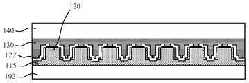
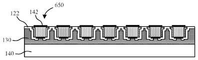
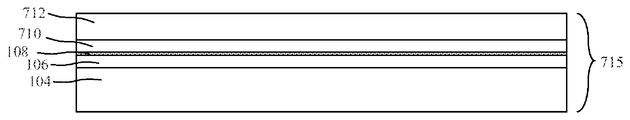
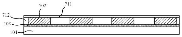
Family Cites Families (41)
| Publication number | Priority date | Publication date | Assignee | Title |
|---|---|---|---|---|
| JPH0680855B2 (ja) * | 1984-04-19 | 1994-10-12 | 日本電気株式会社 | 埋め込み構造半導体レーザ |
| JPS62162383A (ja) * | 1986-01-11 | 1987-07-18 | Fumio Inaba | 半導体発光装置 |
| JPS63143889A (ja) * | 1986-12-08 | 1988-06-16 | Ricoh Co Ltd | 半導体発光装置 |
| JPS63196089A (ja) | 1987-02-10 | 1988-08-15 | Furukawa Electric Co Ltd:The | 半導体発光素子の製造方法 |
| JPH02114675A (ja) * | 1988-10-25 | 1990-04-26 | Sumitomo Electric Ind Ltd | 半導体発光素子ならびにその製造方法 |
| US5138624A (en) | 1989-11-16 | 1992-08-11 | The Boeing Company | Multiwavelength LED and laser diode optical source |
| JP2655943B2 (ja) * | 1991-02-28 | 1997-09-24 | シャープ株式会社 | 半導体発光素子及びその製造方法 |
| JPH0555711A (ja) | 1991-08-22 | 1993-03-05 | Furukawa Electric Co Ltd:The | 半導体レーザ素子とその製造方法 |
| JP2812024B2 (ja) * | 1991-10-17 | 1998-10-15 | 日本電気株式会社 | 面発光素子の製造方法 |
| JPH05218498A (ja) | 1992-02-03 | 1993-08-27 | Mitsubishi Kasei Corp | 横方向に接合を有する発光ダイオード |
| JPH05275802A (ja) * | 1992-03-27 | 1993-10-22 | Fuji Xerox Co Ltd | 半導体レーザの製造方法 |
| JPH06163981A (ja) * | 1992-11-25 | 1994-06-10 | Victor Co Of Japan Ltd | 半導体装置 |
| US5614734A (en) | 1995-03-15 | 1997-03-25 | Yale University | High efficency LED structure |
| JPH09162441A (ja) * | 1995-12-05 | 1997-06-20 | Toshiba Corp | 半導体装置及びその製造方法 |
| JP3782230B2 (ja) * | 1998-03-30 | 2006-06-07 | 株式会社東芝 | 半導体レーザ装置の製造方法及びiii−v族化合物半導体素子の製造方法 |
| DE10039435A1 (de) * | 2000-08-11 | 2002-02-28 | Osram Opto Semiconductors Gmbh | Strahlungsemittierendes Halbleiterbauelement mit erhöhter Strahlungsauskopplung und Herstellungsverfahren hierfür |
| JP3585817B2 (ja) | 2000-09-04 | 2004-11-04 | ユーディナデバイス株式会社 | レーザダイオードおよびその製造方法 |
| US6891202B2 (en) * | 2001-12-14 | 2005-05-10 | Infinera Corporation | Oxygen-doped Al-containing current blocking layers in active semiconductor devices |
| JP2004281559A (ja) * | 2003-03-13 | 2004-10-07 | Toshiba Corp | 半導体発光素子 |
| US6906353B1 (en) * | 2003-11-17 | 2005-06-14 | Jds Uniphase Corporation | High speed implanted VCSEL |
| DE102004029412A1 (de) * | 2004-02-27 | 2005-10-13 | Osram Opto Semiconductors Gmbh | Strahlungsemittierender Halbleiterchip und Verfahren zur Herstellung eines solchen Halbleiterchips |
| JP4655920B2 (ja) * | 2005-12-22 | 2011-03-23 | 日立電線株式会社 | 半導体発光素子 |
| JP5017865B2 (ja) * | 2006-01-17 | 2012-09-05 | 富士電機株式会社 | 半導体装置 |
| JP4903643B2 (ja) * | 2007-07-12 | 2012-03-28 | 株式会社東芝 | 半導体発光素子 |
| JP5170869B2 (ja) * | 2007-11-05 | 2013-03-27 | 古河電気工業株式会社 | 光半導体素子及び光半導体素子の製造方法 |
| KR100903103B1 (ko) * | 2007-12-05 | 2009-06-16 | 우리엘에스티 주식회사 | 화합물 반도체를 이용한 발광소자 |
| JP2009224480A (ja) * | 2008-03-14 | 2009-10-01 | Panasonic Corp | 2波長半導体レーザ装置 |
| DE102008018928A1 (de) * | 2008-04-15 | 2009-10-22 | Osram Opto Semiconductors Gmbh | Optoelektronisches Halbleiterbauelement und Verfahren zur Herstellung eines optoelektronischen Halbleiterbauelements |
| US20110147704A1 (en) | 2008-08-19 | 2011-06-23 | Lattice Power (Jiangxi) Corporation | Semiconductor light-emitting device with passivation layer |
| EP2316138A1 (en) * | 2008-08-19 | 2011-05-04 | Lattice Power (Jiangxi) Corporation | Method for fabricating semiconductor light-emitting device with double-sided passivation |
| US8232566B2 (en) * | 2009-05-04 | 2012-07-31 | Lg Innotek Co., Ltd. | Light emitting device, package, and system |
| JP5356292B2 (ja) * | 2010-03-19 | 2013-12-04 | 株式会社東芝 | 半導体発光素子及び半導体発光装置 |
| US8237174B2 (en) * | 2010-05-10 | 2012-08-07 | National Central University | LED structure |
| DE102010026518B4 (de) * | 2010-07-08 | 2025-02-27 | OSRAM Opto Semiconductors Gesellschaft mit beschränkter Haftung | Leuchtdiodenchip und Verfahren zur Herstellung einer Mehrzahl von Leuchtdiodenchips |
| US9093818B2 (en) * | 2010-07-15 | 2015-07-28 | The Regents Of The University Of California | Nanopillar optical resonator |
| WO2012123840A1 (en) * | 2011-03-14 | 2012-09-20 | Koninklijke Philips Electronics N.V. | Led having vertical contacts redistributed for flip chip mounting |
| JP6035736B2 (ja) | 2011-10-26 | 2016-11-30 | ソニー株式会社 | 発光素子およびその製造方法、並びに発光装置 |
| JP2014204095A (ja) * | 2013-04-10 | 2014-10-27 | 信越半導体株式会社 | 半導体発光素子及びその製造方法 |
| US8987765B2 (en) * | 2013-06-17 | 2015-03-24 | LuxVue Technology Corporation | Reflective bank structure and method for integrating a light emitting device |
| US8928021B1 (en) | 2013-06-18 | 2015-01-06 | LuxVue Technology Corporation | LED light pipe |
| US9450147B2 (en) | 2013-12-27 | 2016-09-20 | Apple Inc. | LED with internally confined current injection area |
-
2015
- 2015-09-14 US US14/853,614 patent/US9484492B2/en active Active
- 2015-12-07 KR KR1020197027276A patent/KR20190109586A/ko not_active Withdrawn
- 2015-12-07 KR KR1020177020694A patent/KR20170100611A/ko not_active Ceased
- 2015-12-07 KR KR1020217018569A patent/KR102380538B1/ko active Active
- 2015-12-07 CN CN201580076368.9A patent/CN107408603B/zh active Active
- 2015-12-07 JP JP2017553307A patent/JP2018505567A/ja active Pending
- 2015-12-07 WO PCT/US2015/064295 patent/WO2016111789A1/en not_active Ceased
- 2015-12-07 EP EP15812919.7A patent/EP3243223B1/en active Active
-
2019
- 2019-11-08 JP JP2019202959A patent/JP2020036038A/ja active Pending
Also Published As
| Publication number | Publication date |
|---|---|
| KR20210076197A (ko) | 2021-06-23 |
| CN107408603A (zh) | 2017-11-28 |
| EP3243223B1 (en) | 2022-06-08 |
| KR20170100611A (ko) | 2017-09-04 |
| EP3243223A1 (en) | 2017-11-15 |
| US9484492B2 (en) | 2016-11-01 |
| CN107408603B (zh) | 2020-04-14 |
| WO2016111789A1 (en) | 2016-07-14 |
| US20160197232A1 (en) | 2016-07-07 |
| JP2020036038A (ja) | 2020-03-05 |
| KR102380538B1 (ko) | 2022-03-29 |
| JP2018505567A (ja) | 2018-02-22 |
Similar Documents
| Publication | Publication Date | Title |
|---|---|---|
| KR102380538B1 (ko) | 비방사 측벽 재결합 감소를 위한 led 구조체 | |
| US10714655B2 (en) | LED structures for reduced non-radiative sidewall recombination | |
| US9601659B2 (en) | LED structures for reduced non-radiative sidewall recombination | |
| US11978825B2 (en) | LED with internally confined current injection area | |
| KR102630680B1 (ko) | Led 소자, led 소자의 제조 방법 및 led 소자를 포함하는 디스플레이 패널 | |
| US9219197B1 (en) | Micro-light-emitting diode | |
| CN109155345B (zh) | 用于减少的非辐射侧壁复合的led结构 | |
| TWI829038B (zh) | 電壓可控的單片原生rgb陣列 | |
| US10662511B2 (en) | Nitride semiconductor light-emitting device, and method for manufacturing same | |
| TW202139483A (zh) | 高分辨率單體式rgb陣列 |
Legal Events
| Date | Code | Title | Description |
|---|---|---|---|
| A107 | Divisional application of patent | ||
| PA0104 | Divisional application for international application |
Comment text: Divisional Application for International Patent Patent event code: PA01041R01D Patent event date: 20190918 Application number text: 1020177020694 Filing date: 20170724 |
|
| PG1501 | Laying open of application | ||
| PC1203 | Withdrawal of no request for examination |