JP5011069B2 - 小さな寄生抵抗を有する低電圧ダイオードおよび製造方法 - Google Patents
小さな寄生抵抗を有する低電圧ダイオードおよび製造方法 Download PDFInfo
- Publication number
- JP5011069B2 JP5011069B2 JP2007292302A JP2007292302A JP5011069B2 JP 5011069 B2 JP5011069 B2 JP 5011069B2 JP 2007292302 A JP2007292302 A JP 2007292302A JP 2007292302 A JP2007292302 A JP 2007292302A JP 5011069 B2 JP5011069 B2 JP 5011069B2
- Authority
- JP
- Japan
- Prior art keywords
- layer
- diode
- substrate
- depositing
- barrier
- Prior art date
- Legal status (The legal status is an assumption and is not a legal conclusion. Google has not performed a legal analysis and makes no representation as to the accuracy of the status listed.)
- Active
Links
Images


Classifications
-
- H—ELECTRICITY
- H10—SEMICONDUCTOR DEVICES; ELECTRIC SOLID-STATE DEVICES NOT OTHERWISE PROVIDED FOR
- H10D—INORGANIC ELECTRIC SEMICONDUCTOR DEVICES
- H10D30/00—Field-effect transistors [FET]
- H10D30/60—Insulated-gate field-effect transistors [IGFET]
- H10D30/67—Thin-film transistors [TFT]
- H10D30/6729—Thin-film transistors [TFT] characterised by the electrodes
- H10D30/6737—Thin-film transistors [TFT] characterised by the electrodes characterised by the electrode materials
- H10D30/6738—Schottky barrier electrodes
-
- H—ELECTRICITY
- H10—SEMICONDUCTOR DEVICES; ELECTRIC SOLID-STATE DEVICES NOT OTHERWISE PROVIDED FOR
- H10D—INORGANIC ELECTRIC SEMICONDUCTOR DEVICES
- H10D30/00—Field-effect transistors [FET]
- H10D30/60—Insulated-gate field-effect transistors [IGFET]
- H10D30/67—Thin-film transistors [TFT]
- H10D30/674—Thin-film transistors [TFT] characterised by the active materials
- H10D30/675—Group III-V materials, Group II-VI materials, Group IV-VI materials, selenium or tellurium
-
- H—ELECTRICITY
- H10—SEMICONDUCTOR DEVICES; ELECTRIC SOLID-STATE DEVICES NOT OTHERWISE PROVIDED FOR
- H10D—INORGANIC ELECTRIC SEMICONDUCTOR DEVICES
- H10D62/00—Semiconductor bodies, or regions thereof, of devices having potential barriers
- H10D62/80—Semiconductor bodies, or regions thereof, of devices having potential barriers characterised by the materials
- H10D62/85—Semiconductor bodies, or regions thereof, of devices having potential barriers characterised by the materials being Group III-V materials, e.g. GaAs
-
- H—ELECTRICITY
- H10—SEMICONDUCTOR DEVICES; ELECTRIC SOLID-STATE DEVICES NOT OTHERWISE PROVIDED FOR
- H10D—INORGANIC ELECTRIC SEMICONDUCTOR DEVICES
- H10D64/00—Electrodes of devices having potential barriers
- H10D64/60—Electrodes characterised by their materials
- H10D64/64—Electrodes comprising a Schottky barrier to a semiconductor
-
- H—ELECTRICITY
- H10—SEMICONDUCTOR DEVICES; ELECTRIC SOLID-STATE DEVICES NOT OTHERWISE PROVIDED FOR
- H10D—INORGANIC ELECTRIC SEMICONDUCTOR DEVICES
- H10D8/00—Diodes
- H10D8/01—Manufacture or treatment
- H10D8/051—Manufacture or treatment of Schottky diodes
-
- H—ELECTRICITY
- H10—SEMICONDUCTOR DEVICES; ELECTRIC SOLID-STATE DEVICES NOT OTHERWISE PROVIDED FOR
- H10D—INORGANIC ELECTRIC SEMICONDUCTOR DEVICES
- H10D8/00—Diodes
- H10D8/60—Schottky-barrier diodes
-
- H—ELECTRICITY
- H10—SEMICONDUCTOR DEVICES; ELECTRIC SOLID-STATE DEVICES NOT OTHERWISE PROVIDED FOR
- H10D—INORGANIC ELECTRIC SEMICONDUCTOR DEVICES
- H10D62/00—Semiconductor bodies, or regions thereof, of devices having potential barriers
- H10D62/80—Semiconductor bodies, or regions thereof, of devices having potential barriers characterised by the materials
- H10D62/85—Semiconductor bodies, or regions thereof, of devices having potential barriers characterised by the materials being Group III-V materials, e.g. GaAs
- H10D62/8503—Nitride Group III-V materials, e.g. AlN or GaN
Landscapes
- Electrodes Of Semiconductors (AREA)
Description
Claims (13)
- ダイオードを製造する方法であって、
基板を提供するステップと、
前記基板上に複数の半導体層を付着させるステップと、
前記半導体層上に誘電体層を付着させるステップと、
前記誘電体層の一部分を除去するステップと、
前記誘電体層の除去された部分によって残された空洞の中の前記複数の半導体層上に、ショットキー金属を付着させるステップと、
導電性支持層を提供するステップと、
金属接合層によって前記誘電体層を前記支持層に貼り付けるステップと、
前記基板を除去して、前記半導体層のうちの前記基板に隣接した1つの半導体層を露出させるステップと、
露出された前記半導体層上にオーミックコンタクトを付着させるステップとを備えることを特徴とする方法。 - 複数の半導体層を付着させる前記ステップは、前記基板上にn+半導電性緩衝層を付着させるステップと、前記n+層上にn−半導電層を付着させるステップと、前記n−層上に半導電性障壁層を付着させるステップとを含むことを特徴とする請求項1に記載の方法。
- 前記n+、n−および障壁層の部分を選択的に除去して、前記誘電体層上に前記ショットキー金属を覆うメサ形ダイオード構造を形成するステップをさらに備えることを特徴とする請求項2に記載の方法。
- 前記基板上にn+層を付着させる前記ステップの前に、前記基板上に核生成層を付着させるステップをさらに備えることを特徴とする請求項2に記載の方法。
- 前記n+層は、5×10¹⁷/cm3から5×1019/cm3の不純物濃度を有するようにドープされた厚さ0.5から5μmのGaN層を含むことを特徴とする請求項2から4のいずれか1項に記載の方法。
- 前記n−層は、1×10¹⁵/cm3から1×1017/cm3の不純物濃度を有するようにドープされた厚さ0.5から5μmのGaN層を含むことを特徴とする請求項2から5のいずれか1項に記載の方法。
- 前記障壁層は、厚さ5〜15ÅのAlxGa1−xN層を含み、0.15≦x≦0.45であることを特徴とする請求項2から6のいずれか1項に記載の方法。
- 金属接合層によって前記誘電体層を前記支持層に貼り付ける前記ステップは、Au−Sn共晶ウェハ接合プロセスを使用して前記誘電体層を前記支持層に貼り付けるステップを含むことを特徴とする請求項1から7のいずれか1項に記載の方法。
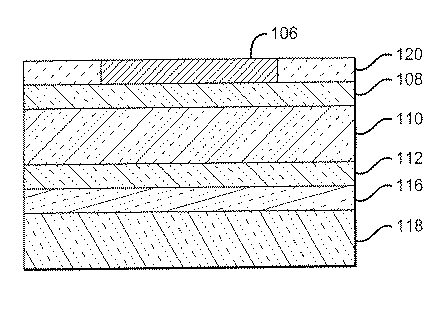
- 導電性支持層と、
前記導電性支持層上に配置された誘電層と、
前記導電性支持層上に配置され、かつ前記誘電層の一部分を除去した後に残った空洞の中に設けられたショットキー金属層と、
前記導電性支持層とは反対側の前記ショットキー金属層上に配置された半導電性障壁層と、
前記ショットキー金属層とは反対側の前記障壁層上に配置されたn−半導電性層と、
前記障壁層とは反対側の前記n−層上に配置されたn+半導体緩衝層であって、当該n+層が予め基板の上に形成された層である、n+半導体緩衝層と、
前記基板が除去された後に、前記n−層とは反対側の前記n+層の表面に配置されたオーミックコンタクトと、
を備えたことを特徴とするダイオード。 - 前記支持層に前記ショットキー金属層を貼り付ける金属接合層をさらに備えることを特徴とする請求項9に記載のダイオード。
- 前記n+層、前記n−層および前記障壁層はIII族窒化物を含むことを特徴とする請求項9に記載のダイオード。
- 前記ショットキー金属は、Cr、Fe、Mn、Nb、Ni、NiCr、Sn、Ta、Ti、GeおよびWからなるグループから選択されることを特徴とする請求項9から11のいずれか1項に記載のダイオード。
- 前記導電性支持層は金属被覆されたSiであることを特徴とする請求項9から12のいずれか1項に記載のダイオード。
Applications Claiming Priority (2)
| Application Number | Priority Date | Filing Date | Title |
|---|---|---|---|
| US11/655,696 | 2007-01-19 | ||
| US11/655,696 US7834367B2 (en) | 2007-01-19 | 2007-01-19 | Low voltage diode with reduced parasitic resistance and method for fabricating |
Publications (2)
| Publication Number | Publication Date |
|---|---|
| JP2008177537A JP2008177537A (ja) | 2008-07-31 |
| JP5011069B2 true JP5011069B2 (ja) | 2012-08-29 |
Family
ID=39312953
Family Applications (1)
| Application Number | Title | Priority Date | Filing Date |
|---|---|---|---|
| JP2007292302A Active JP5011069B2 (ja) | 2007-01-19 | 2007-11-09 | 小さな寄生抵抗を有する低電圧ダイオードおよび製造方法 |
Country Status (3)
| Country | Link |
|---|---|
| US (3) | US7834367B2 (ja) |
| EP (1) | EP1947700B1 (ja) |
| JP (1) | JP5011069B2 (ja) |
Families Citing this family (25)
| Publication number | Priority date | Publication date | Assignee | Title |
|---|---|---|---|---|
| EP2111632A1 (en) * | 2007-02-12 | 2009-10-28 | The Regents of the University of California | Cleaved facet (ga,al,in)n edge-emitting laser diodes grown on semipolar {11-2n} bulk gallium nitride substrates |
| KR20090035869A (ko) * | 2007-10-08 | 2009-04-13 | 삼성전자주식회사 | 유기 반도체 소자 |
| JP5506258B2 (ja) * | 2008-08-06 | 2014-05-28 | キヤノン株式会社 | 整流素子 |
| WO2010110733A1 (en) | 2009-03-25 | 2010-09-30 | Glo Ab | A schottky device |
| US9293644B2 (en) | 2009-09-18 | 2016-03-22 | Soraa, Inc. | Power light emitting diode and method with uniform current density operation |
| US9583678B2 (en) | 2009-09-18 | 2017-02-28 | Soraa, Inc. | High-performance LED fabrication |
| CN107256915A (zh) * | 2009-09-18 | 2017-10-17 | 天空公司 | 发光二极管器件 |
| US8933644B2 (en) | 2009-09-18 | 2015-01-13 | Soraa, Inc. | LED lamps with improved quality of light |
| KR20120032258A (ko) * | 2010-09-28 | 2012-04-05 | 삼성엘이디 주식회사 | 질화갈륨계 반도체소자 및 그 제조방법 |
| WO2013063038A1 (en) * | 2011-10-24 | 2013-05-02 | Rosestreet Labs, Llc | Nitride uv light sensors on silicon substrates |
| US9502992B2 (en) | 2012-06-01 | 2016-11-22 | Coriant Operations, Inc. | Diode substitute with low drop and minimal loading |
| US8981432B2 (en) * | 2012-08-10 | 2015-03-17 | Avogy, Inc. | Method and system for gallium nitride electronic devices using engineered substrates |
| US9761763B2 (en) | 2012-12-21 | 2017-09-12 | Soraa, Inc. | Dense-luminescent-materials-coated violet LEDs |
| US9410664B2 (en) | 2013-08-29 | 2016-08-09 | Soraa, Inc. | Circadian friendly LED light source |
| CN103545405B (zh) * | 2013-11-11 | 2016-03-30 | 天津三安光电有限公司 | 氮化物发光二极管 |
| JP6266490B2 (ja) * | 2014-11-04 | 2018-01-24 | エア・ウォーター株式会社 | 半導体装置およびその製造方法 |
| TWI726964B (zh) * | 2015-12-25 | 2021-05-11 | 日商出光興產股份有限公司 | 積層體 |
| DE102016013542A1 (de) * | 2016-11-14 | 2018-05-17 | 3 - 5 Power Electronics GmbH | Stapelförmige Schottky-Diode |
| US10204778B2 (en) * | 2016-12-28 | 2019-02-12 | QROMIS, Inc. | Method and system for vertical power devices |
| WO2019217842A2 (en) * | 2018-05-10 | 2019-11-14 | University Of Virginia Patent Foundation | System and method for integrating diode sensors on micromachined wafer probes |
| JP2020038939A (ja) * | 2018-09-05 | 2020-03-12 | トレックス・セミコンダクター株式会社 | 縦型化合物半導体デバイスの製造方法 |
| CN110544719A (zh) * | 2019-09-16 | 2019-12-06 | 河北工业大学 | 一种GaN基PIN二极管器件结构及其制备方法 |
| WO2021146596A1 (en) | 2020-01-16 | 2021-07-22 | Matthew Hartensveld | Capacitive control of electrostatic field effect optoelectronic device |
| CN114122106B (zh) * | 2021-10-20 | 2024-04-05 | 苏州科技大学 | 一种开路电压连续可调的肖特基结及其制备和应用 |
| CN115881773B (zh) * | 2022-10-25 | 2025-12-30 | 远山新材料科技有限公司 | 基于AlN衬底的垂直器件及其制造方法 |
Family Cites Families (146)
| Publication number | Priority date | Publication date | Assignee | Title |
|---|---|---|---|---|
| US3896479A (en) | 1973-09-24 | 1975-07-22 | Bell Telephone Labor Inc | Reduced stresses in iii-v semiconductor devices |
| US3886580A (en) * | 1973-10-09 | 1975-05-27 | Cutler Hammer Inc | Tantalum-gallium arsenide schottky barrier semiconductor device |
| US4152044A (en) * | 1977-06-17 | 1979-05-01 | International Telephone And Telegraph Corporation | Galium aluminum arsenide graded index waveguide |
| US4675575A (en) | 1984-07-13 | 1987-06-23 | E & G Enterprises | Light-emitting diode assemblies and systems therefore |
| FR2586844B1 (fr) | 1985-08-27 | 1988-04-29 | Sofrela Sa | Dispositif de signalisation utilisant des diodes electroluminescentes. |
| JPH077180B2 (ja) | 1985-12-12 | 1995-01-30 | コニカ株式会社 | 変倍複写光学系 |
| JPH07120807B2 (ja) | 1986-12-20 | 1995-12-20 | 富士通株式会社 | 定電流半導体装置 |
| JPS63288061A (ja) | 1987-05-20 | 1988-11-25 | Fujitsu Ltd | 半導体負性抵抗素子 |
| US4866005A (en) * | 1987-10-26 | 1989-09-12 | North Carolina State University | Sublimation of silicon carbide to produce large, device quality single crystals of silicon carbide |
| US4946547A (en) * | 1989-10-13 | 1990-08-07 | Cree Research, Inc. | Method of preparing silicon carbide surfaces for crystal growth |
| JPH03191447A (ja) | 1989-12-21 | 1991-08-21 | Nec Corp | デコード方式 |
| US5034783A (en) | 1990-07-27 | 1991-07-23 | At&T Bell Laboratories | Semiconductor device including cascadable polarization independent heterostructure |
| US5200022A (en) * | 1990-10-03 | 1993-04-06 | Cree Research, Inc. | Method of improving mechanically prepared substrate surfaces of alpha silicon carbide for deposition of beta silicon carbide thereon and resulting product |
| JP3068119B2 (ja) | 1991-09-10 | 2000-07-24 | サンケン電気株式会社 | ショットキ障壁を有する半導体装置 |
| JP3173117B2 (ja) | 1992-03-30 | 2001-06-04 | 株式会社村田製作所 | ショットキーバリア半導体装置 |
| DE4228895C2 (de) * | 1992-08-29 | 2002-09-19 | Bosch Gmbh Robert | Kraftfahrzeug-Beleuchtungseinrichtung mit mehreren Halbleiterlichtquellen |
| JP3191447B2 (ja) | 1992-10-21 | 2001-07-23 | 株式会社ニコン | 樹脂接合型非球面レンズの製造方法 |
| JP2932467B2 (ja) | 1993-03-12 | 1999-08-09 | 日亜化学工業株式会社 | 窒化ガリウム系化合物半導体発光素子 |
| US5705321A (en) | 1993-09-30 | 1998-01-06 | The University Of New Mexico | Method for manufacture of quantum sized periodic structures in Si materials |
| JP2932468B2 (ja) | 1993-12-10 | 1999-08-09 | 日亜化学工業株式会社 | 窒化ガリウム系化合物半導体発光素子 |
| JP2800666B2 (ja) | 1993-12-17 | 1998-09-21 | 日亜化学工業株式会社 | 窒化ガリウム系化合物半導体レーザ素子 |
| JP2956489B2 (ja) | 1994-06-24 | 1999-10-04 | 日亜化学工業株式会社 | 窒化ガリウム系化合物半導体の結晶成長方法 |
| JP2890390B2 (ja) | 1994-07-06 | 1999-05-10 | 日亜化学工業株式会社 | 窒化ガリウム系化合物半導体発光素子 |
| JP2790242B2 (ja) | 1994-10-07 | 1998-08-27 | 日亜化学工業株式会社 | 窒化物半導体発光ダイオード |
| JP2921746B2 (ja) | 1995-01-31 | 1999-07-19 | 日亜化学工業株式会社 | 窒化物半導体レーザ素子 |
| US5670798A (en) * | 1995-03-29 | 1997-09-23 | North Carolina State University | Integrated heterostructures of Group III-V nitride semiconductor materials including epitaxial ohmic contact non-nitride buffer layer and methods of fabricating same |
| JP3135041B2 (ja) | 1995-09-29 | 2001-02-13 | 日亜化学工業株式会社 | 窒化物半導体発光素子 |
| JP2900990B2 (ja) | 1995-11-24 | 1999-06-02 | 日亜化学工業株式会社 | 窒化物半導体発光素子 |
| JP2891348B2 (ja) | 1995-11-24 | 1999-05-17 | 日亜化学工業株式会社 | 窒化物半導体レーザ素子 |
| JP3371830B2 (ja) | 1995-11-24 | 2003-01-27 | 日亜化学工業株式会社 | 窒化物半導体発光素子 |
| JP3298390B2 (ja) | 1995-12-11 | 2002-07-02 | 日亜化学工業株式会社 | 窒化物半導体多色発光素子の製造方法 |
| US6388272B1 (en) * | 1996-03-07 | 2002-05-14 | Caldus Semiconductor, Inc. | W/WC/TAC ohmic and rectifying contacts on SiC |
| US5612567A (en) * | 1996-05-13 | 1997-03-18 | North Carolina State University | Schottky barrier rectifiers and methods of forming same |
| JP3366188B2 (ja) | 1996-05-21 | 2003-01-14 | 日亜化学工業株式会社 | 窒化物半導体素子 |
| JP2760344B2 (ja) | 1996-06-12 | 1998-05-28 | 日本電気株式会社 | 照光スイッチ |
| JPH1012969A (ja) | 1996-06-19 | 1998-01-16 | Nichia Chem Ind Ltd | 窒化物半導体レーザ素子 |
| JP3577653B2 (ja) | 1996-07-19 | 2004-10-13 | 松下電器産業株式会社 | 歯科用気体レーザ装置 |
| TW383508B (en) | 1996-07-29 | 2000-03-01 | Nichia Kagaku Kogyo Kk | Light emitting device and display |
| JPH1065271A (ja) | 1996-08-13 | 1998-03-06 | Toshiba Corp | 窒化ガリウム系半導体光発光素子 |
| JP3660446B2 (ja) | 1996-11-07 | 2005-06-15 | 日亜化学工業株式会社 | 窒化物半導体素子及びその製造方法 |
| JP3424465B2 (ja) | 1996-11-15 | 2003-07-07 | 日亜化学工業株式会社 | 窒化物半導体素子及び窒化物半導体の成長方法 |
| CN100485984C (zh) | 1997-01-09 | 2009-05-06 | 日亚化学工业株式会社 | 氮化物半导体元器件 |
| JP3374737B2 (ja) | 1997-01-09 | 2003-02-10 | 日亜化学工業株式会社 | 窒化物半導体素子 |
| FR2759188B1 (fr) | 1997-01-31 | 1999-04-30 | Thery Hindrick | Dispositif de signalisation lumineuse, notamment pour regulation du trafic routier |
| US5767534A (en) | 1997-02-24 | 1998-06-16 | Minnesota Mining And Manufacturing Company | Passivation capping layer for ohmic contact in II-VI semiconductor light transducing device |
| JP3985065B2 (ja) | 1997-05-14 | 2007-10-03 | 忠弘 大見 | 多孔質シリコン基板の形成方法及び多孔質シリコン基板の形成装置 |
| JP3642157B2 (ja) | 1997-05-26 | 2005-04-27 | ソニー株式会社 | p型III族ナイトライド化合物半導体、発光ダイオードおよび半導体レーザ |
| DE19723176C1 (de) | 1997-06-03 | 1998-08-27 | Daimler Benz Ag | Leistungshalbleiter-Bauelement und Verfahren zu dessen Herstellung |
| US6784463B2 (en) * | 1997-06-03 | 2004-08-31 | Lumileds Lighting U.S., Llc | III-Phospide and III-Arsenide flip chip light-emitting devices |
| JP3744211B2 (ja) | 1997-09-01 | 2006-02-08 | 日亜化学工業株式会社 | 窒化物半導体素子 |
| JPH1174562A (ja) | 1997-06-30 | 1999-03-16 | Nichia Chem Ind Ltd | 窒化物半導体素子 |
| DE19729396A1 (de) | 1997-07-09 | 1999-01-14 | Siemens Ag | Elektrischer Kontakt für ein II-VI-Halbleiterbauelement und Verfahren zum Herstellen des elektrischen Kontaktes |
| JP3606015B2 (ja) | 1997-07-23 | 2005-01-05 | 豊田合成株式会社 | 3族窒化物半導体素子の製造方法 |
| EP1014455B1 (en) | 1997-07-25 | 2006-07-12 | Nichia Corporation | Nitride semiconductor device |
| JP3651260B2 (ja) | 1997-10-01 | 2005-05-25 | 日亜化学工業株式会社 | 窒化物半導体素子 |
| JPH11238945A (ja) | 1997-12-18 | 1999-08-31 | Nichia Chem Ind Ltd | 窒化物半導体発光素子 |
| JP3647236B2 (ja) | 1997-12-22 | 2005-05-11 | 日亜化学工業株式会社 | 窒化物半導体レーザ素子 |
| JP3468082B2 (ja) | 1998-02-26 | 2003-11-17 | 日亜化学工業株式会社 | 窒化物半導体素子 |
| CA2322490C (en) | 1998-03-12 | 2010-10-26 | Nichia Chemical Industries, Ltd. | Nitride semiconductor device |
| JPH11298090A (ja) | 1998-04-09 | 1999-10-29 | Nichia Chem Ind Ltd | 窒化物半導体素子 |
| WO1999054118A1 (en) | 1998-04-17 | 1999-10-28 | Barberini S.P.A. | Plant and process for automatically gluing polarising lenses |
| JPH11330552A (ja) | 1998-05-18 | 1999-11-30 | Nichia Chem Ind Ltd | 窒化物半導体発光素子及び発光装置 |
| JP3559453B2 (ja) | 1998-06-29 | 2004-09-02 | 株式会社東芝 | 発光素子 |
| JP3817915B2 (ja) | 1998-07-31 | 2006-09-06 | 株式会社デンソー | ショットキーダイオード及びその製造方法 |
| WO2000021143A1 (de) | 1998-10-05 | 2000-04-13 | Osram Opto Semiconductors Gmbh & Co. Ohg | Strahlungsemittierender halbleiterchip |
| JP3063756B1 (ja) | 1998-10-06 | 2000-07-12 | 日亜化学工業株式会社 | 窒化物半導体素子 |
| JP2000133883A (ja) | 1998-10-22 | 2000-05-12 | Nichia Chem Ind Ltd | 窒化物半導体素子 |
| JP2000150920A (ja) | 1998-11-12 | 2000-05-30 | Nippon Telegr & Teleph Corp <Ntt> | ショットキ接合型半導体ダイオード装置の製法 |
| JP3470622B2 (ja) | 1998-11-18 | 2003-11-25 | 日亜化学工業株式会社 | 窒化物半導体発光素子 |
| JP3705047B2 (ja) | 1998-12-15 | 2005-10-12 | 日亜化学工業株式会社 | 窒化物半導体発光素子 |
| US7001536B2 (en) | 1999-03-23 | 2006-02-21 | The Trustees Of Princeton University | Organometallic complexes as phosphorescent emitters in organic LEDs |
| JP3656456B2 (ja) | 1999-04-21 | 2005-06-08 | 日亜化学工業株式会社 | 窒化物半導体素子 |
| DE19918370B4 (de) | 1999-04-22 | 2006-06-08 | Osram Opto Semiconductors Gmbh | LED-Weißlichtquelle mit Linse |
| JP3719047B2 (ja) | 1999-06-07 | 2005-11-24 | 日亜化学工業株式会社 | 窒化物半導体素子 |
| US6515313B1 (en) | 1999-12-02 | 2003-02-04 | Cree Lighting Company | High efficiency light emitters with reduced polarization-induced charges |
| TW465123B (en) | 2000-02-02 | 2001-11-21 | Ind Tech Res Inst | High power white light LED |
| US6447604B1 (en) | 2000-03-13 | 2002-09-10 | Advanced Technology Materials, Inc. | Method for achieving improved epitaxy quality (surface texture and defect density) on free-standing (aluminum, indium, gallium) nitride ((al,in,ga)n) substrates for opto-electronic and electronic devices |
| JP4406490B2 (ja) | 2000-03-14 | 2010-01-27 | 株式会社朝日ラバー | 発光ダイオード |
| US6765242B1 (en) | 2000-04-11 | 2004-07-20 | Sandia Corporation | Npn double heterostructure bipolar transistor with ingaasn base region |
| CN1252837C (zh) | 2000-04-26 | 2006-04-19 | 奥斯兰姆奥普托半导体股份有限两合公司 | 在GaN基板上的发光二极管芯片和用GaN基板上的发光二极管芯片制造发光二极管元件的方法 |
| JP2001332770A (ja) | 2000-05-23 | 2001-11-30 | Koha Co Ltd | Ledチップの樹脂封止方法 |
| CN1203557C (zh) | 2000-05-29 | 2005-05-25 | 电灯专利信托有限公司 | 基于发光二极管的发射白光的照明设备 |
| US6331915B1 (en) | 2000-06-13 | 2001-12-18 | Kenneth J. Myers | Lighting element including light emitting diodes, microprism sheet, reflector, and diffusing agent |
| US6330111B1 (en) * | 2000-06-13 | 2001-12-11 | Kenneth J. Myers, Edward Greenberg | Lighting elements including light emitting diodes, microprism sheet, reflector, and diffusing agent |
| US6737801B2 (en) | 2000-06-28 | 2004-05-18 | The Fox Group, Inc. | Integrated color LED chip |
| US6586762B2 (en) | 2000-07-07 | 2003-07-01 | Nichia Corporation | Nitride semiconductor device with improved lifetime and high output power |
| JP3839236B2 (ja) | 2000-09-18 | 2006-11-01 | 株式会社小糸製作所 | 車両用灯具 |
| JP2002151928A (ja) | 2000-11-08 | 2002-05-24 | Toshiba Corp | アンテナ、及びアンテナを内蔵する電子機器 |
| AT410266B (de) | 2000-12-28 | 2003-03-25 | Tridonic Optoelectronics Gmbh | Lichtquelle mit einem lichtemittierenden element |
| US6611002B2 (en) * | 2001-02-23 | 2003-08-26 | Nitronex Corporation | Gallium nitride material devices and methods including backside vias |
| JP3830083B2 (ja) | 2001-03-07 | 2006-10-04 | スタンレー電気株式会社 | 半導体装置およびその製造方法 |
| US6746889B1 (en) * | 2001-03-27 | 2004-06-08 | Emcore Corporation | Optoelectronic device with improved light extraction |
| JP3645233B2 (ja) | 2001-06-07 | 2005-05-11 | 日本電信電話株式会社 | 半導体素子 |
| US20030015708A1 (en) | 2001-07-23 | 2003-01-23 | Primit Parikh | Gallium nitride based diodes with low forward voltage and low reverse current operation |
| US20030020069A1 (en) | 2001-07-25 | 2003-01-30 | Motorola, Inc. | Structure and method for optimizing transmission media through dielectric layering and doping in semiconductor structures and devices utilizing the formation of a compliant substrate |
| JP4210823B2 (ja) * | 2001-08-20 | 2009-01-21 | サンケン電気株式会社 | シヨットキバリアダイオード及びその製造方法 |
| PL225235B1 (pl) | 2001-10-26 | 2017-03-31 | Ammono Spółka Z Ograniczoną Odpowiedzialnością | Objętościowy monokryształ azotkowy oraz jego zastosowanie jako podłoże do epitaksji |
| US6833564B2 (en) | 2001-11-02 | 2004-12-21 | Lumileds Lighting U.S., Llc | Indium gallium nitride separate confinement heterostructure light emitting devices |
| WO2003044870A1 (fr) | 2001-11-22 | 2003-05-30 | Mireille Georges | Dispositif optique d'eclairage a diodes electroluminescentes |
| WO2003050849A2 (en) | 2001-12-06 | 2003-06-19 | Hrl Laboratories, Llc | High power-low noise microwave gan heterojunction field effet transistor |
| JP3802424B2 (ja) | 2002-01-15 | 2006-07-26 | 株式会社東芝 | 半導体発光素子及びその製造方法 |
| JP3782357B2 (ja) | 2002-01-18 | 2006-06-07 | 株式会社東芝 | 半導体発光素子の製造方法 |
| JP4504610B2 (ja) | 2002-03-01 | 2010-07-14 | 株式会社日立製作所 | リッジ型半導体レーザ素子 |
| JP3878868B2 (ja) | 2002-03-01 | 2007-02-07 | シャープ株式会社 | GaN系レーザ素子 |
| JP3801931B2 (ja) | 2002-03-05 | 2006-07-26 | ローム株式会社 | Ledチップを使用した発光装置の構造及び製造方法 |
| EP1490453B1 (en) | 2002-03-25 | 2012-08-15 | Philips Intellectual Property & Standards GmbH | Tri-color white light led lamp |
| US7262434B2 (en) * | 2002-03-28 | 2007-08-28 | Rohm Co., Ltd. | Semiconductor device with a silicon carbide substrate and ohmic metal layer |
| US7792170B2 (en) | 2002-09-20 | 2010-09-07 | Mitsubishi Chemical Corporation | Semiconductor laser |
| US6815241B2 (en) | 2002-09-25 | 2004-11-09 | Cao Group, Inc. | GaN structures having low dislocation density and methods of manufacture |
| KR100495215B1 (ko) * | 2002-12-27 | 2005-06-14 | 삼성전기주식회사 | 수직구조 갈륨나이트라이드 발광다이오드 및 그 제조방법 |
| US6693357B1 (en) | 2003-03-13 | 2004-02-17 | Texas Instruments Incorporated | Methods and semiconductor devices with wiring layer fill structures to improve planarization uniformity |
| JP4182783B2 (ja) | 2003-03-14 | 2008-11-19 | 豊田合成株式会社 | Ledパッケージ |
| JP4058627B2 (ja) | 2003-03-14 | 2008-03-12 | 株式会社朝日ラバー | 半導体光学素子用樹脂レンズの製造方法 |
| US20040183081A1 (en) | 2003-03-20 | 2004-09-23 | Alexander Shishov | Light emitting diode package with self dosing feature and methods of forming same |
| JP4274843B2 (ja) | 2003-04-21 | 2009-06-10 | シャープ株式会社 | Ledデバイスおよびそれを用いた携帯電話機器、デジタルカメラおよびlcd表示装置 |
| US7087936B2 (en) * | 2003-04-30 | 2006-08-08 | Cree, Inc. | Methods of forming light-emitting devices having an antireflective layer that has a graded index of refraction |
| JP4030463B2 (ja) | 2003-05-20 | 2008-01-09 | 三洋電機株式会社 | Led光源及びその製造方法 |
| WO2004109813A2 (de) | 2003-05-30 | 2004-12-16 | Osram Opto Semiconductors Gmbh | Lumineszenzdiode |
| US20050048766A1 (en) | 2003-08-31 | 2005-03-03 | Wen-Chieh Wu | Method for fabricating a conductive plug in integrated circuit |
| US20050077535A1 (en) | 2003-10-08 | 2005-04-14 | Joinscan Electronics Co., Ltd | LED and its manufacturing process |
| JP4590905B2 (ja) | 2003-10-31 | 2010-12-01 | 豊田合成株式会社 | 発光素子および発光装置 |
| TWI291770B (en) | 2003-11-14 | 2007-12-21 | Hon Hai Prec Ind Co Ltd | Surface light source device and light emitting diode |
| US6932497B1 (en) * | 2003-12-17 | 2005-08-23 | Jean-San Huang | Signal light and rear-view mirror arrangement |
| US7102152B2 (en) | 2004-10-14 | 2006-09-05 | Avago Technologies Ecbu Ip (Singapore) Pte. Ltd. | Device and method for emitting output light using quantum dots and non-quantum fluorescent material |
| JP4442216B2 (ja) | 2003-12-19 | 2010-03-31 | 豊田合成株式会社 | Ledランプ装置 |
| US6943381B2 (en) | 2004-01-30 | 2005-09-13 | Lumileds Lighting U.S., Llc | III-nitride light-emitting devices with improved high-current efficiency |
| US7170111B2 (en) | 2004-02-05 | 2007-01-30 | Cree, Inc. | Nitride heterojunction transistors having charge-transfer induced energy barriers and methods of fabricating the same |
| JP4233466B2 (ja) | 2004-02-12 | 2009-03-04 | 三菱化学株式会社 | 発光装置、照明装置および表示装置 |
| US7517728B2 (en) | 2004-03-31 | 2009-04-14 | Cree, Inc. | Semiconductor light emitting devices including a luminescent conversion element |
| US7514867B2 (en) | 2004-04-19 | 2009-04-07 | Panasonic Corporation | LED lamp provided with optical diffusion layer having increased thickness and method of manufacturing thereof |
| JP4180017B2 (ja) * | 2004-05-17 | 2008-11-12 | 三菱電機株式会社 | ショットキーバリアダイオード |
| US7203409B2 (en) | 2004-08-16 | 2007-04-10 | Covega Corporation | Superluminescent diodes having high output power and reduced internal reflections |
| EP1653255A3 (en) | 2004-10-29 | 2006-06-21 | Pentair Water Pool and Spa, Inc. | Selectable beam lens for underwater light |
| JP4567426B2 (ja) * | 2004-11-25 | 2010-10-20 | パナソニック株式会社 | ショットキーバリアダイオード及びダイオードアレイ |
| JP5140922B2 (ja) | 2005-01-17 | 2013-02-13 | オムロン株式会社 | 発光光源及び発光光源アレイ |
| TWI255566B (en) | 2005-03-04 | 2006-05-21 | Jemitek Electronics Corp | Led |
| US7491626B2 (en) | 2005-06-20 | 2009-02-17 | Sensor Electronic Technology, Inc. | Layer growth using metal film and/or islands |
| CN101223638A (zh) * | 2005-07-05 | 2008-07-16 | 国际整流器公司 | 具有改进的浪涌能力的肖特基二极管 |
| JP2007036010A (ja) * | 2005-07-28 | 2007-02-08 | Toshiba Corp | ショットキーバリアダイオード装置及びその製造方法 |
| CN100449888C (zh) | 2005-07-29 | 2009-01-07 | 日亚化学工业株式会社 | 半导体激光元件 |
| EP2372223A3 (en) | 2005-12-21 | 2012-08-01 | Cree, Inc. | Lighting Device and Lighting Method |
| WO2007121486A2 (en) | 2006-04-18 | 2007-10-25 | Lamina Lighting, Inc. | Optical devices for controlled color mixing |
| KR100850950B1 (ko) | 2006-07-26 | 2008-08-08 | 엘지전자 주식회사 | 질화물계 발광 소자 |
| US7820075B2 (en) | 2006-08-10 | 2010-10-26 | Intematix Corporation | Phosphor composition with self-adjusting chromaticity |
| US9012937B2 (en) | 2007-10-10 | 2015-04-21 | Cree, Inc. | Multiple conversion material light emitting diode package and method of fabricating same |
| DE102007057674A1 (de) * | 2007-11-30 | 2009-06-04 | Osram Opto Semiconductors Gmbh | LED mit Stromaufweitungsschicht |
-
2007
- 2007-01-19 US US11/655,696 patent/US7834367B2/en active Active
- 2007-11-09 JP JP2007292302A patent/JP5011069B2/ja active Active
- 2007-11-16 EP EP07254498.4A patent/EP1947700B1/en active Active
-
2010
- 2010-10-15 US US12/905,374 patent/US8344398B2/en active Active
-
2012
- 2012-12-04 US US13/693,929 patent/US9041139B2/en active Active
Also Published As
| Publication number | Publication date |
|---|---|
| US7834367B2 (en) | 2010-11-16 |
| US9041139B2 (en) | 2015-05-26 |
| US20080173882A1 (en) | 2008-07-24 |
| EP1947700A2 (en) | 2008-07-23 |
| EP1947700B1 (en) | 2016-01-06 |
| US20110031579A1 (en) | 2011-02-10 |
| EP1947700A3 (en) | 2010-01-13 |
| JP2008177537A (ja) | 2008-07-31 |
| US20130126894A1 (en) | 2013-05-23 |
| US8344398B2 (en) | 2013-01-01 |
Similar Documents
| Publication | Publication Date | Title |
|---|---|---|
| JP5011069B2 (ja) | 小さな寄生抵抗を有する低電圧ダイオードおよび製造方法 | |
| US11121216B2 (en) | III-nitride devices including a graded depleting layer | |
| US11342420B2 (en) | Heterojunction devices and methods for fabricating the same | |
| TWI395320B (zh) | 氮化鎵半導體裝置 | |
| CN104201210B (zh) | 二极管以及包括该二极管的组件 | |
| US20230017518A1 (en) | Semiconductor device | |
| CN100373634C (zh) | 具有低正向电压及低反向电流操作的氮化镓基底的二极管 | |
| JP6308478B2 (ja) | 一部が凹んだアノードを有するGaN系ショットキーダイオード | |
| US9608092B2 (en) | Method of manufacturing a semiconductor device having a rectifying junction at the side wall of a trench | |
| US9525039B2 (en) | Method of fabricating a merged P-N junction and schottky diode with regrown gallium nitride layer | |
| US9236434B2 (en) | Semiconductor device and manufacturing method thereof | |
| JP2016502761A (ja) | ショットキーダイオード及びその製造方法 | |
| JP2016501442A (ja) | デュアルメタルの、一部が凹んだ電極を有する、GaN系ショットキーダイオード | |
| WO2014025722A2 (en) | Method and system for gallium nitride electronic devices using engineered substrates | |
| US20130119437A1 (en) | Semiconductor device | |
| US20240113235A1 (en) | Silicon carbide device with single metallization process for ohmic and schottky contacts | |
| US8274128B2 (en) | Semiconductor device with buffer layer | |
| CN111276530A (zh) | 半导体器件及其制造方法 |
Legal Events
| Date | Code | Title | Description |
|---|---|---|---|
| A521 | Request for written amendment filed |
Free format text: JAPANESE INTERMEDIATE CODE: A523 Effective date: 20080605 |
|
| A621 | Written request for application examination |
Free format text: JAPANESE INTERMEDIATE CODE: A621 Effective date: 20080605 |
|
| RD02 | Notification of acceptance of power of attorney |
Free format text: JAPANESE INTERMEDIATE CODE: A7422 Effective date: 20100928 |
|
| RD04 | Notification of resignation of power of attorney |
Free format text: JAPANESE INTERMEDIATE CODE: A7424 Effective date: 20101012 |
|
| A131 | Notification of reasons for refusal |
Free format text: JAPANESE INTERMEDIATE CODE: A131 Effective date: 20111004 |
|
| A977 | Report on retrieval |
Free format text: JAPANESE INTERMEDIATE CODE: A971007 Effective date: 20111006 |
|
| A521 | Request for written amendment filed |
Free format text: JAPANESE INTERMEDIATE CODE: A523 Effective date: 20120104 |
|
| A131 | Notification of reasons for refusal |
Free format text: JAPANESE INTERMEDIATE CODE: A131 Effective date: 20120124 |
|
| A521 | Request for written amendment filed |
Free format text: JAPANESE INTERMEDIATE CODE: A523 Effective date: 20120420 |
|
| TRDD | Decision of grant or rejection written | ||
| A01 | Written decision to grant a patent or to grant a registration (utility model) |
Free format text: JAPANESE INTERMEDIATE CODE: A01 Effective date: 20120515 |
|
| A01 | Written decision to grant a patent or to grant a registration (utility model) |
Free format text: JAPANESE INTERMEDIATE CODE: A01 |
|
| A61 | First payment of annual fees (during grant procedure) |
Free format text: JAPANESE INTERMEDIATE CODE: A61 Effective date: 20120604 |
|
| R150 | Certificate of patent or registration of utility model |
Ref document number: 5011069 Country of ref document: JP Free format text: JAPANESE INTERMEDIATE CODE: R150 Free format text: JAPANESE INTERMEDIATE CODE: R150 |
|
| FPAY | Renewal fee payment (event date is renewal date of database) |
Free format text: PAYMENT UNTIL: 20150608 Year of fee payment: 3 |
|
| FPAY | Renewal fee payment (event date is renewal date of database) |
Free format text: PAYMENT UNTIL: 20150608 Year of fee payment: 3 |
|
| RD02 | Notification of acceptance of power of attorney |
Free format text: JAPANESE INTERMEDIATE CODE: R3D02 |
|
| FPAY | Renewal fee payment (event date is renewal date of database) |
Free format text: PAYMENT UNTIL: 20150608 Year of fee payment: 3 |
|
| RD04 | Notification of resignation of power of attorney |
Free format text: JAPANESE INTERMEDIATE CODE: R3D04 |
|
| R250 | Receipt of annual fees |
Free format text: JAPANESE INTERMEDIATE CODE: R250 |
|
| R250 | Receipt of annual fees |
Free format text: JAPANESE INTERMEDIATE CODE: R250 |
|
| R250 | Receipt of annual fees |
Free format text: JAPANESE INTERMEDIATE CODE: R250 |
|
| R250 | Receipt of annual fees |
Free format text: JAPANESE INTERMEDIATE CODE: R250 |
|
| R250 | Receipt of annual fees |
Free format text: JAPANESE INTERMEDIATE CODE: R250 |
|
| R250 | Receipt of annual fees |
Free format text: JAPANESE INTERMEDIATE CODE: R250 |
|
| R250 | Receipt of annual fees |
Free format text: JAPANESE INTERMEDIATE CODE: R250 |
|
| R250 | Receipt of annual fees |
Free format text: JAPANESE INTERMEDIATE CODE: R250 |
|
| R250 | Receipt of annual fees |
Free format text: JAPANESE INTERMEDIATE CODE: R250 |
|
| R250 | Receipt of annual fees |
Free format text: JAPANESE INTERMEDIATE CODE: R250 |
|
| R250 | Receipt of annual fees |
Free format text: JAPANESE INTERMEDIATE CODE: R250 |