JP4553376B2 - 浮上式基板搬送処理装置及び浮上式基板搬送処理方法 - Google Patents
浮上式基板搬送処理装置及び浮上式基板搬送処理方法 Download PDFInfo
- Publication number
- JP4553376B2 JP4553376B2 JP2005208851A JP2005208851A JP4553376B2 JP 4553376 B2 JP4553376 B2 JP 4553376B2 JP 2005208851 A JP2005208851 A JP 2005208851A JP 2005208851 A JP2005208851 A JP 2005208851A JP 4553376 B2 JP4553376 B2 JP 4553376B2
- Authority
- JP
- Japan
- Prior art keywords
- substrate
- floating
- processed
- suction
- stage
- Prior art date
- Legal status (The legal status is an assumption and is not a legal conclusion. Google has not performed a legal analysis and makes no representation as to the accuracy of the status listed.)
- Active
Links
- 239000000758 substrate Substances 0.000 title claims description 188
- 238000012545 processing Methods 0.000 title claims description 108
- 238000007667 floating Methods 0.000 title claims description 70
- 238000012546 transfer Methods 0.000 title claims description 41
- 238000003672 processing method Methods 0.000 title claims description 9
- 238000005339 levitation Methods 0.000 claims description 23
- 239000007788 liquid Substances 0.000 claims description 20
- 238000000576 coating method Methods 0.000 description 26
- 239000011248 coating agent Substances 0.000 description 25
- 230000032258 transport Effects 0.000 description 21
- 238000002347 injection Methods 0.000 description 15
- 239000007924 injection Substances 0.000 description 15
- 230000007723 transport mechanism Effects 0.000 description 10
- 238000000034 method Methods 0.000 description 9
- 239000000243 solution Substances 0.000 description 8
- 230000010349 pulsation Effects 0.000 description 7
- 238000011161 development Methods 0.000 description 6
- 239000011521 glass Substances 0.000 description 5
- 230000008569 process Effects 0.000 description 5
- 238000004140 cleaning Methods 0.000 description 4
- 238000009281 ultraviolet germicidal irradiation Methods 0.000 description 4
- 239000011230 binding agent Substances 0.000 description 3
- 238000001816 cooling Methods 0.000 description 3
- 230000002093 peripheral effect Effects 0.000 description 3
- 239000000126 substance Substances 0.000 description 3
- 238000010586 diagram Methods 0.000 description 2
- 238000001035 drying Methods 0.000 description 2
- 238000004519 manufacturing process Methods 0.000 description 2
- 238000001179 sorption measurement Methods 0.000 description 2
- 241000255777 Lepidoptera Species 0.000 description 1
- 229910052782 aluminium Inorganic materials 0.000 description 1
- XAGFODPZIPBFFR-UHFFFAOYSA-N aluminium Chemical compound [Al] XAGFODPZIPBFFR-UHFFFAOYSA-N 0.000 description 1
- 238000007796 conventional method Methods 0.000 description 1
- 238000002788 crimping Methods 0.000 description 1
- 230000006837 decompression Effects 0.000 description 1
- 238000009826 distribution Methods 0.000 description 1
- 238000005516 engineering process Methods 0.000 description 1
- 238000010030 laminating Methods 0.000 description 1
- 229910052751 metal Inorganic materials 0.000 description 1
- 239000002184 metal Substances 0.000 description 1
- 238000012986 modification Methods 0.000 description 1
- 230000004048 modification Effects 0.000 description 1
- 238000000206 photolithography Methods 0.000 description 1
- 239000011148 porous material Substances 0.000 description 1
- 238000011160 research Methods 0.000 description 1
- 229920005989 resin Polymers 0.000 description 1
- 239000011347 resin Substances 0.000 description 1
- 230000004044 response Effects 0.000 description 1
- 239000004065 semiconductor Substances 0.000 description 1
- 239000002904 solvent Substances 0.000 description 1
- 229910001220 stainless steel Inorganic materials 0.000 description 1
- 239000010935 stainless steel Substances 0.000 description 1
- 230000001629 suppression Effects 0.000 description 1
- 229920003002 synthetic resin Polymers 0.000 description 1
- 239000000057 synthetic resin Substances 0.000 description 1
- 238000001291 vacuum drying Methods 0.000 description 1
Images


Classifications
-
- G—PHYSICS
- G02—OPTICS
- G02F—OPTICAL DEVICES OR ARRANGEMENTS FOR THE CONTROL OF LIGHT BY MODIFICATION OF THE OPTICAL PROPERTIES OF THE MEDIA OF THE ELEMENTS INVOLVED THEREIN; NON-LINEAR OPTICS; FREQUENCY-CHANGING OF LIGHT; OPTICAL LOGIC ELEMENTS; OPTICAL ANALOGUE/DIGITAL CONVERTERS
- G02F1/00—Devices or arrangements for the control of the intensity, colour, phase, polarisation or direction of light arriving from an independent light source, e.g. switching, gating or modulating; Non-linear optics
- G02F1/01—Devices or arrangements for the control of the intensity, colour, phase, polarisation or direction of light arriving from an independent light source, e.g. switching, gating or modulating; Non-linear optics for the control of the intensity, phase, polarisation or colour
- G02F1/13—Devices or arrangements for the control of the intensity, colour, phase, polarisation or direction of light arriving from an independent light source, e.g. switching, gating or modulating; Non-linear optics for the control of the intensity, phase, polarisation or colour based on liquid crystals, e.g. single liquid crystal display cells
-
- H—ELECTRICITY
- H01—ELECTRIC ELEMENTS
- H01L—SEMICONDUCTOR DEVICES NOT COVERED BY CLASS H10
- H01L21/00—Processes or apparatus adapted for the manufacture or treatment of semiconductor or solid state devices or of parts thereof
- H01L21/67—Apparatus specially adapted for handling semiconductor or electric solid state devices during manufacture or treatment thereof; Apparatus specially adapted for handling wafers during manufacture or treatment of semiconductor or electric solid state devices or components ; Apparatus not specifically provided for elsewhere
- H01L21/67005—Apparatus not specifically provided for elsewhere
- H01L21/67011—Apparatus for manufacture or treatment
- H01L21/6715—Apparatus for applying a liquid, a resin, an ink or the like
-
- H—ELECTRICITY
- H01—ELECTRIC ELEMENTS
- H01L—SEMICONDUCTOR DEVICES NOT COVERED BY CLASS H10
- H01L21/00—Processes or apparatus adapted for the manufacture or treatment of semiconductor or solid state devices or of parts thereof
- H01L21/67—Apparatus specially adapted for handling semiconductor or electric solid state devices during manufacture or treatment thereof; Apparatus specially adapted for handling wafers during manufacture or treatment of semiconductor or electric solid state devices or components ; Apparatus not specifically provided for elsewhere
- H01L21/677—Apparatus specially adapted for handling semiconductor or electric solid state devices during manufacture or treatment thereof; Apparatus specially adapted for handling wafers during manufacture or treatment of semiconductor or electric solid state devices or components ; Apparatus not specifically provided for elsewhere for conveying, e.g. between different workstations
- H01L21/67739—Apparatus specially adapted for handling semiconductor or electric solid state devices during manufacture or treatment thereof; Apparatus specially adapted for handling wafers during manufacture or treatment of semiconductor or electric solid state devices or components ; Apparatus not specifically provided for elsewhere for conveying, e.g. between different workstations into and out of processing chamber
- H01L21/6776—Continuous loading and unloading into and out of a processing chamber, e.g. transporting belts within processing chambers
-
- H—ELECTRICITY
- H01—ELECTRIC ELEMENTS
- H01L—SEMICONDUCTOR DEVICES NOT COVERED BY CLASS H10
- H01L21/00—Processes or apparatus adapted for the manufacture or treatment of semiconductor or solid state devices or of parts thereof
- H01L21/67—Apparatus specially adapted for handling semiconductor or electric solid state devices during manufacture or treatment thereof; Apparatus specially adapted for handling wafers during manufacture or treatment of semiconductor or electric solid state devices or components ; Apparatus not specifically provided for elsewhere
- H01L21/677—Apparatus specially adapted for handling semiconductor or electric solid state devices during manufacture or treatment thereof; Apparatus specially adapted for handling wafers during manufacture or treatment of semiconductor or electric solid state devices or components ; Apparatus not specifically provided for elsewhere for conveying, e.g. between different workstations
- H01L21/67784—Apparatus specially adapted for handling semiconductor or electric solid state devices during manufacture or treatment thereof; Apparatus specially adapted for handling wafers during manufacture or treatment of semiconductor or electric solid state devices or components ; Apparatus not specifically provided for elsewhere for conveying, e.g. between different workstations using air tracks
-
- H—ELECTRICITY
- H01—ELECTRIC ELEMENTS
- H01L—SEMICONDUCTOR DEVICES NOT COVERED BY CLASS H10
- H01L21/00—Processes or apparatus adapted for the manufacture or treatment of semiconductor or solid state devices or of parts thereof
- H01L21/67—Apparatus specially adapted for handling semiconductor or electric solid state devices during manufacture or treatment thereof; Apparatus specially adapted for handling wafers during manufacture or treatment of semiconductor or electric solid state devices or components ; Apparatus not specifically provided for elsewhere
- H01L21/683—Apparatus specially adapted for handling semiconductor or electric solid state devices during manufacture or treatment thereof; Apparatus specially adapted for handling wafers during manufacture or treatment of semiconductor or electric solid state devices or components ; Apparatus not specifically provided for elsewhere for supporting or gripping
- H01L21/6838—Apparatus specially adapted for handling semiconductor or electric solid state devices during manufacture or treatment thereof; Apparatus specially adapted for handling wafers during manufacture or treatment of semiconductor or electric solid state devices or components ; Apparatus not specifically provided for elsewhere for supporting or gripping with gripping and holding devices using a vacuum; Bernoulli devices
-
- B—PERFORMING OPERATIONS; TRANSPORTING
- B05—SPRAYING OR ATOMISING IN GENERAL; APPLYING FLUENT MATERIALS TO SURFACES, IN GENERAL
- B05C—APPARATUS FOR APPLYING FLUENT MATERIALS TO SURFACES, IN GENERAL
- B05C5/00—Apparatus in which liquid or other fluent material is projected, poured or allowed to flow on to the surface of the work
- B05C5/02—Apparatus in which liquid or other fluent material is projected, poured or allowed to flow on to the surface of the work the liquid or other fluent material being discharged through an outlet orifice by pressure, e.g. from an outlet device in contact or almost in contact, with the work
- B05C5/0208—Apparatus in which liquid or other fluent material is projected, poured or allowed to flow on to the surface of the work the liquid or other fluent material being discharged through an outlet orifice by pressure, e.g. from an outlet device in contact or almost in contact, with the work for applying liquid or other fluent material to separate articles
Description
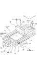
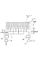
図2は、上記レジスト塗布処理装置20の第1実施形態の要部を示す概略斜視図、図3は、レジスト塗布処理装置20における気体の供給及び吸引状態を示す概略構成図、図4及び図5は、気体の供給及び吸引状態を示す要部断面図である。
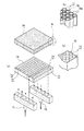
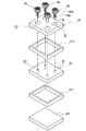
図8は、この発明に係る浮上式基板搬送処理装置の第2実施形態の要部を示す概略断面図、図9は、第2実施形態における気体(空気)の供給及び吸引部を示す要部分解斜視図(a)、(a)のII部を示す拡大斜視図(b)及びII部を示す別の拡大斜視図(c)である。
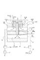
図11は、この発明に係る浮上式基板搬送処理装置の第3実施形態の要部を示す概略断面図、図12は、第3実施形態における気体(空気)の供給及び吸引部を示す要部分解斜視図である。
なお、上記実施形態では、この発明に係る浮上式基板搬送処理装置をレジスト塗布処理装置に適用した場合について説明したが、レジスト塗布処理装置以外の装置、例えば現像処理装置にも適用できることは勿論である。
22,22A,22B 浮上ステージ
23 レジスト供給ノズル(処理液供給手段)
24 基板保持部材
28 リニアモータ(移動手段)
50 多孔質部材
51 多孔質部(気体供給孔)
52 吸引孔
55 コンプレッサ(気体供給手段)
56 迂回流路
57 真空ポンプ(吸引手段)
70 多孔板
71 小孔
72 気体供給流路溝
72a 直状主溝
72b 枝溝
73 気体吸引流路溝
73a 直状主溝
73b 枝溝
80 表面板
81 大径孔
82 中間板
83 小径孔
84 下部板
85 ステージ本体
86 多孔体
86a 大径頭部
86b 脚部
88 Oリング(シール部材)
91 第1の空間
92 第2の空間
Claims (4)
- 表面から気体を噴射及び吸引して被処理基板を浮上する浮上ステージと、
上記浮上ステージの上方に配置され、上記被処理基板の表面に処理液を供給する処理液供給手段と、
上記被処理基板の両側端をそれぞれ着脱可能に保持すると共に、被処理基板を上記浮上ステージ上で移動する移動手段と、を具備する浮上式基板搬送処理装置において、
上記浮上ステージを多孔質部材にて形成すると共に、該多孔質部材に気密に区画される複数の吸引孔を設け、
上記多孔質部材の多孔質部に気体供給手段を接続し、
上記吸引孔に迂回流路を介して吸引手段を接続し、
上記複数の吸引孔を被処理基板の搬送方向及び該搬送方向と直交する方向の直線上に一致しないよう傾斜状に配列する、ことを特徴とする浮上式基板搬送処理装置。 - 表面から気体を噴射及び吸引して被処理基板を浮上する浮上ステージと、
上記浮上ステージの上方に配置され、上記被処理基板の表面に処理液を供給する処理液供給手段と、
上記被処理基板の両側端をそれぞれ着脱可能に保持すると共に、被処理基板を上記浮上ステージ上で移動する移動手段と、を具備する浮上式基板搬送処理装置において、
上記浮上ステージは、複数の大径孔を設けた表面板と、該表面板の下面との間に第1の空間をおいて配設されると共に、上記大径孔の直下に位置する小径孔を設けた中間板と、該中間板の下面との間に第2の空間をおいて配設される下部板とからなるステージ本体と、
整列された多数の小孔を有し、上記大径孔に嵌合する大径頭部の下部に上記小径孔に気密に嵌合する脚部を有する多孔体と、を具備し、
上記第1又は第2の空間のいずれか一方に気体供給手段を接続すると共に、他方の空間に吸引手段を接続してなる、ことを特徴とする浮上式基板搬送処理装置。 - 請求項1記載の浮上式基板搬送処理装置を用いた浮上式基板搬送処理方法であって、
浮上ステージを形成する多孔質部材の多孔質部により圧力損失を受けて分散される気体を供給すると共に、多孔質部材に気密に区画される複数の吸引孔から圧力損失を与える迂回流路を介して吸引して、浮上ステージ上に被処理基板を浮上し、上記被処理基板の表面に処理液供給手段から処理液を帯状に供給すると共に、移動手段によって被処理基板を移動する、ことを特徴とする浮上式基板搬送処理方法。 - 請求項2記載の浮上式基板搬送処理装置を用いた浮上式基板搬送処理方法であって、
浮上ステージを形成する第1の空間又は第2の空間を介して多孔板の多数の小孔により圧力損失を受けて分散される気体を供給すると共に、多孔板の多数の小孔から上記第2の空間又は第1の空間を介して吸引して、浮上ステージ上に被処理基板を浮上し、上記被処理基板の表面に処理液供給手段から処理液を帯状に供給すると共に、移動手段によって被処理基板を移動する、ことを特徴とする浮上式基板搬送処理方法。
Priority Applications (5)
| Application Number | Priority Date | Filing Date | Title |
|---|---|---|---|
| JP2005208851A JP4553376B2 (ja) | 2005-07-19 | 2005-07-19 | 浮上式基板搬送処理装置及び浮上式基板搬送処理方法 |
| US11/486,005 US7905195B2 (en) | 2005-07-19 | 2006-07-14 | Floating-type substrate conveying and processing apparatus |
| TW095126266A TWI336113B (en) | 2005-07-19 | 2006-07-18 | Surfacing type substrate transportation processing apparatus and surfacing type substrate transportation processing method |
| TW099107296A TWI438857B (zh) | 2005-07-19 | 2006-07-18 | 浮上式基板搬送處理裝置及浮上式基板搬送處理方法 |
| KR1020060067297A KR101100486B1 (ko) | 2005-07-19 | 2006-07-19 | 부상식 기판 반송 처리 장치 |
Applications Claiming Priority (1)
| Application Number | Priority Date | Filing Date | Title |
|---|---|---|---|
| JP2005208851A JP4553376B2 (ja) | 2005-07-19 | 2005-07-19 | 浮上式基板搬送処理装置及び浮上式基板搬送処理方法 |
Publications (3)
| Publication Number | Publication Date |
|---|---|
| JP2007027495A JP2007027495A (ja) | 2007-02-01 |
| JP2007027495A5 JP2007027495A5 (ja) | 2007-07-05 |
| JP4553376B2 true JP4553376B2 (ja) | 2010-09-29 |
Family
ID=37677905
Family Applications (1)
| Application Number | Title | Priority Date | Filing Date |
|---|---|---|---|
| JP2005208851A Active JP4553376B2 (ja) | 2005-07-19 | 2005-07-19 | 浮上式基板搬送処理装置及び浮上式基板搬送処理方法 |
Country Status (4)
| Country | Link |
|---|---|
| US (1) | US7905195B2 (ja) |
| JP (1) | JP4553376B2 (ja) |
| KR (1) | KR101100486B1 (ja) |
| TW (2) | TWI336113B (ja) |
Cited By (1)
| Publication number | Priority date | Publication date | Assignee | Title |
|---|---|---|---|---|
| CN110404717A (zh) * | 2019-06-14 | 2019-11-05 | 上海维誉自动化设备有限公司 | 一种自动喷涂线 |
Families Citing this family (74)
| Publication number | Priority date | Publication date | Assignee | Title |
|---|---|---|---|---|
| JPWO2007105455A1 (ja) * | 2006-02-28 | 2009-07-30 | 株式会社アルバック | ステージ装置 |
| WO2007145072A1 (ja) * | 2006-06-14 | 2007-12-21 | Nsk Ltd. | 支持装置 |
| JP5047545B2 (ja) * | 2006-06-30 | 2012-10-10 | 株式会社妙徳 | 浮上搬送ユニット |
| JP4652351B2 (ja) * | 2007-02-02 | 2011-03-16 | 大日本印刷株式会社 | 基板支持装置、基板支持方法 |
| JP4743716B2 (ja) * | 2007-03-06 | 2011-08-10 | 東京エレクトロン株式会社 | 基板処理装置 |
| JP4982292B2 (ja) * | 2007-08-07 | 2012-07-25 | 東京応化工業株式会社 | 塗布装置及び塗布方法 |
| JP5188759B2 (ja) * | 2007-08-07 | 2013-04-24 | 東京応化工業株式会社 | 塗布装置及び塗布方法 |
| JP2009043829A (ja) * | 2007-08-07 | 2009-02-26 | Tokyo Ohka Kogyo Co Ltd | 塗布装置及び塗布方法 |
| JP4942589B2 (ja) * | 2007-08-30 | 2012-05-30 | 東京応化工業株式会社 | 塗布装置及び塗布方法 |
| JP4384686B2 (ja) * | 2007-09-25 | 2009-12-16 | 東京エレクトロン株式会社 | 常圧乾燥装置及び基板処理装置及び基板処理方法 |
| JP4991495B2 (ja) * | 2007-11-26 | 2012-08-01 | 東京エレクトロン株式会社 | 検査用保持部材及び検査用保持部材の製造方法 |
| JP5029486B2 (ja) | 2008-05-13 | 2012-09-19 | 東京エレクトロン株式会社 | 塗布装置、塗布方法及び記憶媒体 |
| JP5012651B2 (ja) | 2008-05-14 | 2012-08-29 | 東京エレクトロン株式会社 | 塗布装置、塗布方法、塗布、現像装置及び記憶媒体 |
| JP4857312B2 (ja) * | 2008-07-16 | 2012-01-18 | シャープ株式会社 | 基板搬送装置 |
| JP4972618B2 (ja) * | 2008-08-05 | 2012-07-11 | シャープ株式会社 | 基板搬送装置 |
| JP2010037082A (ja) * | 2008-08-07 | 2010-02-18 | Sharp Corp | 基板搬送装置および基板搬送方法 |
| KR101296659B1 (ko) * | 2008-11-14 | 2013-08-14 | 엘지디스플레이 주식회사 | 세정 장치 |
| US20110042874A1 (en) * | 2009-08-20 | 2011-02-24 | Nikon Corporation | Object processing apparatus, exposure apparatus and exposure method, and device manufacturing method |
| US8699001B2 (en) * | 2009-08-20 | 2014-04-15 | Nikon Corporation | Object moving apparatus, object processing apparatus, exposure apparatus, object inspecting apparatus and device manufacturing method |
| KR101862234B1 (ko) * | 2009-08-20 | 2018-05-29 | 가부시키가이샤 니콘 | 물체 처리 장치, 노광 장치와 노광 방법, 및 디바이스 제조 방법 |
| KR101069600B1 (ko) | 2009-09-01 | 2011-10-05 | 주식회사 케이씨텍 | 부상식 기판 코터 장치 및 그 코팅 방법 |
| WO2012119034A2 (en) * | 2011-03-02 | 2012-09-07 | Game Changers, Llc | Method and apparatus for a dynamic air cushion transport system |
| JP4919115B2 (ja) * | 2009-09-24 | 2012-04-18 | 横河電機株式会社 | 放射線検査装置 |
| KR101158267B1 (ko) * | 2009-10-26 | 2012-06-19 | 주식회사 나래나노텍 | 기판 부상 유닛에 사용되는 부상 플레이트, 및 이를 구비한 기판 부상 유닛, 기판 이송 장치 및 코팅 장치 |
| KR101141146B1 (ko) * | 2009-12-30 | 2012-05-02 | 주식회사 케이씨텍 | 기판 반송 방법 |
| KR101099555B1 (ko) * | 2010-01-12 | 2011-12-28 | 세메스 주식회사 | 기판 처리 장치 |
| US20110239231A1 (en) * | 2010-03-23 | 2011-09-29 | International Business Machines Corporation | Migrating electronic document version contents and version metadata as a collection with a single operation |
| JP5465595B2 (ja) * | 2010-05-10 | 2014-04-09 | オイレス工業株式会社 | 非接触搬送装置 |
| EP2388808A1 (de) * | 2010-05-20 | 2011-11-23 | Westfälische Wilhelms-Universität Münster | Berührungsloses Transportsystem |
| US8598538B2 (en) | 2010-09-07 | 2013-12-03 | Nikon Corporation | Movable body apparatus, object processing device, exposure apparatus, flat-panel display manufacturing method, and device manufacturing method |
| JP5913131B2 (ja) * | 2010-12-24 | 2016-04-27 | オイレス工業株式会社 | 上昇流形成体及びこの上昇流形成体を用いた非接触搬送装置 |
| JP5663297B2 (ja) * | 2010-12-27 | 2015-02-04 | 東京応化工業株式会社 | 塗布装置 |
| CN102543662B (zh) * | 2010-12-30 | 2016-02-03 | 上海微电子装备有限公司 | 热盘及应用其的硅片加热系统 |
| KR20140031180A (ko) * | 2011-01-14 | 2014-03-12 | 오일레스고교 가부시키가이샤 | 비접촉 반송장치 |
| US9136155B2 (en) * | 2011-11-17 | 2015-09-15 | Lam Research Ag | Method and device for processing wafer shaped articles |
| KR101312364B1 (ko) * | 2011-12-22 | 2013-09-27 | 주식회사 나래나노텍 | 기판 착탈 장치 및 방법, 및 이를 구비한 코팅 장치 및 방법 |
| JP5912642B2 (ja) * | 2012-02-20 | 2016-04-27 | 日本電気硝子株式会社 | ガラス板の搬送装置及びその搬送方法 |
| TWI527747B (zh) * | 2012-02-28 | 2016-04-01 | 炭研軸封精工股份有限公司 | 非接觸吸著盤 |
| KR101423822B1 (ko) * | 2012-06-28 | 2014-07-28 | 세메스 주식회사 | 웨이퍼 이송을 위한 비접촉 척 |
| JP5987528B2 (ja) * | 2012-07-30 | 2016-09-07 | 株式会社タンケンシールセーコウ | 浮上装置 |
| US9387993B2 (en) * | 2012-10-30 | 2016-07-12 | Nissan Motor Co., Ltd. | Conveyor apparatus |
| JP2014218342A (ja) * | 2013-05-09 | 2014-11-20 | オイレス工業株式会社 | 支持用エアプレートおよびその気体流抵抗器 |
| JP6226419B2 (ja) * | 2013-08-22 | 2017-11-08 | オイレス工業株式会社 | 浮上搬送装置 |
| JP6339341B2 (ja) * | 2013-10-11 | 2018-06-06 | 平田機工株式会社 | 処理システム及び処理方法 |
| JP6270114B2 (ja) * | 2013-11-20 | 2018-01-31 | 東レエンジニアリング株式会社 | 基板浮上装置 |
| KR101963489B1 (ko) * | 2014-04-30 | 2019-07-31 | 카티바, 인크. | 가스 쿠션 장비 및 기판 코팅 기술 |
| US10332770B2 (en) * | 2014-09-24 | 2019-06-25 | Sandisk Technologies Llc | Wafer transfer system |
| JP6949455B2 (ja) | 2014-12-24 | 2021-10-13 | 株式会社タンケンシールセーコウ | 非接触搬送装置、および非接触吸着盤 |
| TWI735438B (zh) * | 2015-03-30 | 2021-08-11 | 日商尼康股份有限公司 | 物體搬運裝置、曝光裝置、平板顯示器的製造方法、元件製造方法、物體搬運方法以及曝光方法 |
| KR102584657B1 (ko) * | 2015-03-31 | 2023-10-04 | 가부시키가이샤 니콘 | 노광 장치, 플랫 패널 디스플레이의 제조 방법, 디바이스 제조 방법, 및 노광 방법 |
| JP6215281B2 (ja) * | 2015-10-27 | 2017-10-18 | 株式会社日本製鋼所 | 被処理体搬送装置、半導体製造装置および被処理体搬送方法 |
| JP6651392B2 (ja) * | 2016-03-22 | 2020-02-19 | 東レエンジニアリング株式会社 | 基板浮上搬送装置 |
| KR101690189B1 (ko) * | 2016-03-23 | 2016-12-27 | (주) 세명유리 | 거울 유리의 엣지 자동 방수코팅 장치 |
| FR3049941B1 (fr) * | 2016-04-06 | 2018-04-13 | Saint- Gobain Glass France | Dispositif de convoyage et de maintien pour feuille de verre notamment dans une installation de lavage |
| US9633878B1 (en) | 2016-04-21 | 2017-04-25 | Texas Instuments Incorporated | Conveyor apparatus and method for transporting leadframe |
| US10689209B2 (en) * | 2016-06-21 | 2020-06-23 | Core Flow Ltd. | Noncontact support platform with edge lifting |
| US10179707B2 (en) * | 2016-06-30 | 2019-01-15 | Ace Machinary Co., Ltd. | Transfer apparatus |
| WO2018001709A1 (en) * | 2016-07-01 | 2018-01-04 | Asml Netherlands B.V. | Stage system, lithographic apparatus, method for positioning and device manufacturing method |
| JP6854605B2 (ja) | 2016-08-29 | 2021-04-07 | 株式会社日本製鋼所 | レーザ照射装置、レーザ照射方法、及び半導体装置の製造方法 |
| JP6910518B2 (ja) * | 2016-08-29 | 2021-07-28 | 株式会社日本製鋼所 | レーザ照射装置 |
| JP6917691B2 (ja) * | 2016-10-04 | 2021-08-11 | 株式会社日本製鋼所 | レーザ照射装置、レーザ照射方法、及び半導体装置の製造方法 |
| JP6819373B2 (ja) * | 2017-03-10 | 2021-01-27 | 株式会社Ihi | 浮上装置及びテンション検出装置 |
| US9889995B1 (en) * | 2017-03-15 | 2018-02-13 | Core Flow Ltd. | Noncontact support platform with blockage detection |
| JP6983578B2 (ja) * | 2017-08-25 | 2021-12-17 | 株式会社日本製鋼所 | レーザ照射装置、レーザ照射方法、及び半導体装置の製造方法 |
| WO2019186402A1 (en) * | 2018-03-28 | 2019-10-03 | Biemme Elettrica Di Bertola Massimo | Device for coating, in particular painting, the main surfaces of rigid panels with liquid products |
| JP7034817B2 (ja) * | 2018-04-19 | 2022-03-14 | 株式会社日本製鋼所 | レーザ処理装置及び半導体装置の製造方法 |
| JP7110005B2 (ja) * | 2018-06-20 | 2022-08-01 | キヤノン株式会社 | 基板回転装置、基板回転方法、リソグラフィ装置、および物品製造方法 |
| CN109633939B (zh) * | 2018-12-27 | 2024-04-16 | 苏州精濑光电有限公司 | 一种lcd检测设备 |
| US20200266092A1 (en) * | 2019-02-19 | 2020-08-20 | Corning Incorporated | Apparatuses and methods for non-contact holding and measurement of thin substrates |
| JP7299790B2 (ja) * | 2019-08-05 | 2023-06-28 | 東レエンジニアリング株式会社 | 基板浮上搬送装置及び基板浮上搬送装置の基板位置補正方法 |
| KR102268617B1 (ko) * | 2019-10-16 | 2021-06-23 | 세메스 주식회사 | 기판 처리 장치 |
| CN113130368A (zh) * | 2021-04-13 | 2021-07-16 | 南京中安半导体设备有限责任公司 | 气浮卡盘及晶圆几何参数测量装置 |
| JP7095166B2 (ja) * | 2020-08-21 | 2022-07-04 | Jswアクティナシステム株式会社 | レーザ照射装置、レーザ照射方法、及び半導体装置の製造方法 |
| IT202100013085A1 (it) * | 2021-05-20 | 2022-11-20 | Cefla Soc Cooperativa | Apparato e metodo per la verniciatura a rullo di pannelli, preferibilmente pannelli fotovoltaici |
Citations (9)
| Publication number | Priority date | Publication date | Assignee | Title |
|---|---|---|---|---|
| JP2000072251A (ja) * | 1998-08-31 | 2000-03-07 | Watanabe Shoko:Kk | 浮上搬送装置および浮上搬送システム |
| JP2000128346A (ja) * | 1998-08-20 | 2000-05-09 | Matsushita Electric Ind Co Ltd | 浮揚装置、浮揚搬送装置および熱処理装置 |
| JP2000159342A (ja) * | 1998-11-20 | 2000-06-13 | Daiichi Shisetsu Kogyo Kk | 板状部材の搬送装置 |
| JP2004262608A (ja) * | 2003-03-03 | 2004-09-24 | Orbotech Ltd | 空気浮上装置 |
| JP2004273574A (ja) * | 2003-03-05 | 2004-09-30 | Wakomu Denso:Kk | 基板浮上装置および同方法 |
| JP2004331265A (ja) * | 2003-05-01 | 2004-11-25 | Olympus Corp | 浮上ユニット及び基板検査装置 |
| JP2004345744A (ja) * | 2003-05-20 | 2004-12-09 | Hitachi Zosen Corp | 空気浮上装置および空気浮上式搬送装置 |
| JP2005132626A (ja) * | 2003-10-06 | 2005-05-26 | Sumitomo Heavy Ind Ltd | 搬送装置、塗布システム、及び検査システム |
| JP2006237097A (ja) * | 2005-02-23 | 2006-09-07 | Tokyo Electron Ltd | ステージ装置および塗布処理装置 |
Family Cites Families (7)
| Publication number | Priority date | Publication date | Assignee | Title |
|---|---|---|---|---|
| ES2054357T3 (es) * | 1989-05-08 | 1994-08-01 | Philips Nv | Aparato y metodo para tratar substratos planos bajo una presion reducida. |
| DE59406900D1 (de) * | 1993-02-08 | 1998-10-22 | Sez Semiconduct Equip Zubehoer | Träger für scheibenförmige Gegenstände |
| JP3245813B2 (ja) | 1996-11-27 | 2002-01-15 | 東京エレクトロン株式会社 | 塗布膜形成装置 |
| JP4398786B2 (ja) | 2003-07-23 | 2010-01-13 | 東京エレクトロン株式会社 | 塗布方法及び塗布装置 |
| JP4305918B2 (ja) | 2004-01-30 | 2009-07-29 | 東京エレクトロン株式会社 | 浮上式基板搬送処理装置 |
| KR101112029B1 (ko) * | 2004-02-13 | 2012-03-21 | 에이에스엠 아메리카, 인코포레이티드 | 자동 도핑 및 후면 증착의 감소를 위한 기판 지지 시스템 |
| WO2005099350A2 (en) * | 2004-04-14 | 2005-10-27 | Coreflow Scientific Solutions Ltd. | Non-contact support platforms for distance adjustment |
-
2005
- 2005-07-19 JP JP2005208851A patent/JP4553376B2/ja active Active
-
2006
- 2006-07-14 US US11/486,005 patent/US7905195B2/en not_active Expired - Fee Related
- 2006-07-18 TW TW095126266A patent/TWI336113B/zh not_active IP Right Cessation
- 2006-07-18 TW TW099107296A patent/TWI438857B/zh active
- 2006-07-19 KR KR1020060067297A patent/KR101100486B1/ko active IP Right Grant
Patent Citations (9)
| Publication number | Priority date | Publication date | Assignee | Title |
|---|---|---|---|---|
| JP2000128346A (ja) * | 1998-08-20 | 2000-05-09 | Matsushita Electric Ind Co Ltd | 浮揚装置、浮揚搬送装置および熱処理装置 |
| JP2000072251A (ja) * | 1998-08-31 | 2000-03-07 | Watanabe Shoko:Kk | 浮上搬送装置および浮上搬送システム |
| JP2000159342A (ja) * | 1998-11-20 | 2000-06-13 | Daiichi Shisetsu Kogyo Kk | 板状部材の搬送装置 |
| JP2004262608A (ja) * | 2003-03-03 | 2004-09-24 | Orbotech Ltd | 空気浮上装置 |
| JP2004273574A (ja) * | 2003-03-05 | 2004-09-30 | Wakomu Denso:Kk | 基板浮上装置および同方法 |
| JP2004331265A (ja) * | 2003-05-01 | 2004-11-25 | Olympus Corp | 浮上ユニット及び基板検査装置 |
| JP2004345744A (ja) * | 2003-05-20 | 2004-12-09 | Hitachi Zosen Corp | 空気浮上装置および空気浮上式搬送装置 |
| JP2005132626A (ja) * | 2003-10-06 | 2005-05-26 | Sumitomo Heavy Ind Ltd | 搬送装置、塗布システム、及び検査システム |
| JP2006237097A (ja) * | 2005-02-23 | 2006-09-07 | Tokyo Electron Ltd | ステージ装置および塗布処理装置 |
Cited By (1)
| Publication number | Priority date | Publication date | Assignee | Title |
|---|---|---|---|---|
| CN110404717A (zh) * | 2019-06-14 | 2019-11-05 | 上海维誉自动化设备有限公司 | 一种自动喷涂线 |
Also Published As
| Publication number | Publication date |
|---|---|
| US7905195B2 (en) | 2011-03-15 |
| JP2007027495A (ja) | 2007-02-01 |
| KR101100486B1 (ko) | 2011-12-29 |
| TWI336113B (en) | 2011-01-11 |
| TW201025488A (en) | 2010-07-01 |
| TW200731449A (en) | 2007-08-16 |
| US20070017442A1 (en) | 2007-01-25 |
| TWI438857B (zh) | 2014-05-21 |
| KR20070011153A (ko) | 2007-01-24 |
Similar Documents
| Publication | Publication Date | Title |
|---|---|---|
| JP4553376B2 (ja) | 浮上式基板搬送処理装置及び浮上式基板搬送処理方法 | |
| JP2007027495A5 (ja) | ||
| JP4305918B2 (ja) | 浮上式基板搬送処理装置 | |
| JP4033841B2 (ja) | 浮上式基板搬送処理方法及びその装置 | |
| JP4554397B2 (ja) | ステージ装置および塗布処理装置 | |
| JP4571525B2 (ja) | 基板処理装置及び基板処理方法 | |
| KR101087845B1 (ko) | 도포 처리 장치 및 도포 처리 방법 | |
| JP2006237482A (ja) | 基板処理装置及び基板処理方法及び基板処理プログラム | |
| JP2006206324A (ja) | 基板搬送装置 | |
| JP4319175B2 (ja) | 減圧乾燥装置 | |
| JP2010098125A (ja) | 基板搬送装置及び基板搬送方法 | |
| KR100837849B1 (ko) | 처리액 공급방법 및 처리액 공급장치 | |
| TWI462215B (zh) | 基板處理裝置、轉換方法、及轉移方法 | |
| JP2009018917A (ja) | 塗布装置、基板の受け渡し方法及び塗布方法 | |
| KR20100035119A (ko) | 감압 건조 장치 및 감압 건조 방법 | |
| JP2005247516A (ja) | 浮上式基板搬送処理装置 | |
| JP5221508B2 (ja) | 基板処理装置 | |
| JP5165718B2 (ja) | 基板処理装置 | |
| KR101344926B1 (ko) | 지지유닛, 이를 포함하는 기판처리장치 | |
| JP6595276B2 (ja) | 基板処理装置および基板処理方法 | |
| KR20180124891A (ko) | 기판 부상 반송 장치 | |
| JP2018143942A (ja) | 塗布装置および塗布方法 | |
| JP4386430B2 (ja) | 塗布膜形成装置 | |
| JP2014013804A (ja) | 塗布処理装置、塗布処理方法、プログラム及びコンピュータ記憶媒体 | |
| TW200841414A (en) | Substrate conveyance system |
Legal Events
| Date | Code | Title | Description |
|---|---|---|---|
| A521 | Request for written amendment filed |
Free format text: JAPANESE INTERMEDIATE CODE: A523 Effective date: 20070517 |
|
| A621 | Written request for application examination |
Free format text: JAPANESE INTERMEDIATE CODE: A621 Effective date: 20070517 |
|
| A131 | Notification of reasons for refusal |
Free format text: JAPANESE INTERMEDIATE CODE: A131 Effective date: 20100107 |
|
| A521 | Request for written amendment filed |
Free format text: JAPANESE INTERMEDIATE CODE: A523 Effective date: 20100226 |
|
| A131 | Notification of reasons for refusal |
Free format text: JAPANESE INTERMEDIATE CODE: A131 Effective date: 20100510 |
|
| A521 | Request for written amendment filed |
Free format text: JAPANESE INTERMEDIATE CODE: A523 Effective date: 20100624 |
|
| TRDD | Decision of grant or rejection written | ||
| A01 | Written decision to grant a patent or to grant a registration (utility model) |
Free format text: JAPANESE INTERMEDIATE CODE: A01 Effective date: 20100712 |
|
| A01 | Written decision to grant a patent or to grant a registration (utility model) |
Free format text: JAPANESE INTERMEDIATE CODE: A01 |
|
| A61 | First payment of annual fees (during grant procedure) |
Free format text: JAPANESE INTERMEDIATE CODE: A61 Effective date: 20100712 |
|
| FPAY | Renewal fee payment (event date is renewal date of database) |
Free format text: PAYMENT UNTIL: 20130723 Year of fee payment: 3 |
|
| R150 | Certificate of patent or registration of utility model |
Ref document number: 4553376 Country of ref document: JP Free format text: JAPANESE INTERMEDIATE CODE: R150 Free format text: JAPANESE INTERMEDIATE CODE: R150 |
|
| R250 | Receipt of annual fees |
Free format text: JAPANESE INTERMEDIATE CODE: R250 |
|
| R250 | Receipt of annual fees |
Free format text: JAPANESE INTERMEDIATE CODE: R250 |
|
| R250 | Receipt of annual fees |
Free format text: JAPANESE INTERMEDIATE CODE: R250 |
|
| R250 | Receipt of annual fees |
Free format text: JAPANESE INTERMEDIATE CODE: R250 |
|
| R250 | Receipt of annual fees |
Free format text: JAPANESE INTERMEDIATE CODE: R250 |
|
| R250 | Receipt of annual fees |
Free format text: JAPANESE INTERMEDIATE CODE: R250 |
|
| R250 | Receipt of annual fees |
Free format text: JAPANESE INTERMEDIATE CODE: R250 |