JP4553376B2 - Floating substrate transfer processing apparatus and floating substrate transfer processing method - Google Patents
Floating substrate transfer processing apparatus and floating substrate transfer processing method Download PDFInfo
- Publication number
- JP4553376B2 JP4553376B2 JP2005208851A JP2005208851A JP4553376B2 JP 4553376 B2 JP4553376 B2 JP 4553376B2 JP 2005208851 A JP2005208851 A JP 2005208851A JP 2005208851 A JP2005208851 A JP 2005208851A JP 4553376 B2 JP4553376 B2 JP 4553376B2
- Authority
- JP
- Japan
- Prior art keywords
- substrate
- floating
- processed
- suction
- stage
- Prior art date
- Legal status (The legal status is an assumption and is not a legal conclusion. Google has not performed a legal analysis and makes no representation as to the accuracy of the status listed.)
- Active
Links
- 239000000758 substrate Substances 0.000 title claims description 188
- 238000012545 processing Methods 0.000 title claims description 108
- 238000007667 floating Methods 0.000 title claims description 70
- 238000012546 transfer Methods 0.000 title claims description 41
- 238000003672 processing method Methods 0.000 title claims description 9
- 238000005339 levitation Methods 0.000 claims description 23
- 239000007788 liquid Substances 0.000 claims description 20
- 238000000576 coating method Methods 0.000 description 26
- 239000011248 coating agent Substances 0.000 description 25
- 230000032258 transport Effects 0.000 description 21
- 238000002347 injection Methods 0.000 description 15
- 239000007924 injection Substances 0.000 description 15
- 230000007723 transport mechanism Effects 0.000 description 10
- 238000000034 method Methods 0.000 description 9
- 239000000243 solution Substances 0.000 description 8
- 230000010349 pulsation Effects 0.000 description 7
- 238000011161 development Methods 0.000 description 6
- 239000011521 glass Substances 0.000 description 5
- 230000008569 process Effects 0.000 description 5
- 238000004140 cleaning Methods 0.000 description 4
- 238000009281 ultraviolet germicidal irradiation Methods 0.000 description 4
- 239000011230 binding agent Substances 0.000 description 3
- 238000001816 cooling Methods 0.000 description 3
- 230000002093 peripheral effect Effects 0.000 description 3
- 239000000126 substance Substances 0.000 description 3
- 238000010586 diagram Methods 0.000 description 2
- 238000001035 drying Methods 0.000 description 2
- 238000004519 manufacturing process Methods 0.000 description 2
- 238000001179 sorption measurement Methods 0.000 description 2
- 241000255777 Lepidoptera Species 0.000 description 1
- 229910052782 aluminium Inorganic materials 0.000 description 1
- XAGFODPZIPBFFR-UHFFFAOYSA-N aluminium Chemical compound [Al] XAGFODPZIPBFFR-UHFFFAOYSA-N 0.000 description 1
- 238000007796 conventional method Methods 0.000 description 1
- 238000002788 crimping Methods 0.000 description 1
- 230000006837 decompression Effects 0.000 description 1
- 238000009826 distribution Methods 0.000 description 1
- 238000005516 engineering process Methods 0.000 description 1
- 238000010030 laminating Methods 0.000 description 1
- 229910052751 metal Inorganic materials 0.000 description 1
- 239000002184 metal Substances 0.000 description 1
- 238000012986 modification Methods 0.000 description 1
- 230000004048 modification Effects 0.000 description 1
- 238000000206 photolithography Methods 0.000 description 1
- 239000011148 porous material Substances 0.000 description 1
- 238000011160 research Methods 0.000 description 1
- 229920005989 resin Polymers 0.000 description 1
- 239000011347 resin Substances 0.000 description 1
- 230000004044 response Effects 0.000 description 1
- 239000004065 semiconductor Substances 0.000 description 1
- 239000002904 solvent Substances 0.000 description 1
- 229910001220 stainless steel Inorganic materials 0.000 description 1
- 239000010935 stainless steel Substances 0.000 description 1
- 230000001629 suppression Effects 0.000 description 1
- 229920003002 synthetic resin Polymers 0.000 description 1
- 239000000057 synthetic resin Substances 0.000 description 1
- 238000001291 vacuum drying Methods 0.000 description 1
Images


Classifications
-
- G—PHYSICS
- G02—OPTICS
- G02F—OPTICAL DEVICES OR ARRANGEMENTS FOR THE CONTROL OF LIGHT BY MODIFICATION OF THE OPTICAL PROPERTIES OF THE MEDIA OF THE ELEMENTS INVOLVED THEREIN; NON-LINEAR OPTICS; FREQUENCY-CHANGING OF LIGHT; OPTICAL LOGIC ELEMENTS; OPTICAL ANALOGUE/DIGITAL CONVERTERS
- G02F1/00—Devices or arrangements for the control of the intensity, colour, phase, polarisation or direction of light arriving from an independent light source, e.g. switching, gating or modulating; Non-linear optics
- G02F1/01—Devices or arrangements for the control of the intensity, colour, phase, polarisation or direction of light arriving from an independent light source, e.g. switching, gating or modulating; Non-linear optics for the control of the intensity, phase, polarisation or colour
- G02F1/13—Devices or arrangements for the control of the intensity, colour, phase, polarisation or direction of light arriving from an independent light source, e.g. switching, gating or modulating; Non-linear optics for the control of the intensity, phase, polarisation or colour based on liquid crystals, e.g. single liquid crystal display cells
-
- H—ELECTRICITY
- H01—ELECTRIC ELEMENTS
- H01L—SEMICONDUCTOR DEVICES NOT COVERED BY CLASS H10
- H01L21/00—Processes or apparatus adapted for the manufacture or treatment of semiconductor or solid state devices or of parts thereof
- H01L21/67—Apparatus specially adapted for handling semiconductor or electric solid state devices during manufacture or treatment thereof; Apparatus specially adapted for handling wafers during manufacture or treatment of semiconductor or electric solid state devices or components ; Apparatus not specifically provided for elsewhere
- H01L21/67005—Apparatus not specifically provided for elsewhere
- H01L21/67011—Apparatus for manufacture or treatment
- H01L21/6715—Apparatus for applying a liquid, a resin, an ink or the like
-
- H—ELECTRICITY
- H01—ELECTRIC ELEMENTS
- H01L—SEMICONDUCTOR DEVICES NOT COVERED BY CLASS H10
- H01L21/00—Processes or apparatus adapted for the manufacture or treatment of semiconductor or solid state devices or of parts thereof
- H01L21/67—Apparatus specially adapted for handling semiconductor or electric solid state devices during manufacture or treatment thereof; Apparatus specially adapted for handling wafers during manufacture or treatment of semiconductor or electric solid state devices or components ; Apparatus not specifically provided for elsewhere
- H01L21/677—Apparatus specially adapted for handling semiconductor or electric solid state devices during manufacture or treatment thereof; Apparatus specially adapted for handling wafers during manufacture or treatment of semiconductor or electric solid state devices or components ; Apparatus not specifically provided for elsewhere for conveying, e.g. between different workstations
- H01L21/67739—Apparatus specially adapted for handling semiconductor or electric solid state devices during manufacture or treatment thereof; Apparatus specially adapted for handling wafers during manufacture or treatment of semiconductor or electric solid state devices or components ; Apparatus not specifically provided for elsewhere for conveying, e.g. between different workstations into and out of processing chamber
- H01L21/6776—Continuous loading and unloading into and out of a processing chamber, e.g. transporting belts within processing chambers
-
- H—ELECTRICITY
- H01—ELECTRIC ELEMENTS
- H01L—SEMICONDUCTOR DEVICES NOT COVERED BY CLASS H10
- H01L21/00—Processes or apparatus adapted for the manufacture or treatment of semiconductor or solid state devices or of parts thereof
- H01L21/67—Apparatus specially adapted for handling semiconductor or electric solid state devices during manufacture or treatment thereof; Apparatus specially adapted for handling wafers during manufacture or treatment of semiconductor or electric solid state devices or components ; Apparatus not specifically provided for elsewhere
- H01L21/677—Apparatus specially adapted for handling semiconductor or electric solid state devices during manufacture or treatment thereof; Apparatus specially adapted for handling wafers during manufacture or treatment of semiconductor or electric solid state devices or components ; Apparatus not specifically provided for elsewhere for conveying, e.g. between different workstations
- H01L21/67784—Apparatus specially adapted for handling semiconductor or electric solid state devices during manufacture or treatment thereof; Apparatus specially adapted for handling wafers during manufacture or treatment of semiconductor or electric solid state devices or components ; Apparatus not specifically provided for elsewhere for conveying, e.g. between different workstations using air tracks
-
- H—ELECTRICITY
- H01—ELECTRIC ELEMENTS
- H01L—SEMICONDUCTOR DEVICES NOT COVERED BY CLASS H10
- H01L21/00—Processes or apparatus adapted for the manufacture or treatment of semiconductor or solid state devices or of parts thereof
- H01L21/67—Apparatus specially adapted for handling semiconductor or electric solid state devices during manufacture or treatment thereof; Apparatus specially adapted for handling wafers during manufacture or treatment of semiconductor or electric solid state devices or components ; Apparatus not specifically provided for elsewhere
- H01L21/683—Apparatus specially adapted for handling semiconductor or electric solid state devices during manufacture or treatment thereof; Apparatus specially adapted for handling wafers during manufacture or treatment of semiconductor or electric solid state devices or components ; Apparatus not specifically provided for elsewhere for supporting or gripping
- H01L21/6838—Apparatus specially adapted for handling semiconductor or electric solid state devices during manufacture or treatment thereof; Apparatus specially adapted for handling wafers during manufacture or treatment of semiconductor or electric solid state devices or components ; Apparatus not specifically provided for elsewhere for supporting or gripping with gripping and holding devices using a vacuum; Bernoulli devices
-
- B—PERFORMING OPERATIONS; TRANSPORTING
- B05—SPRAYING OR ATOMISING IN GENERAL; APPLYING FLUENT MATERIALS TO SURFACES, IN GENERAL
- B05C—APPARATUS FOR APPLYING FLUENT MATERIALS TO SURFACES, IN GENERAL
- B05C5/00—Apparatus in which liquid or other fluent material is projected, poured or allowed to flow on to the surface of the work
- B05C5/02—Apparatus in which liquid or other fluent material is projected, poured or allowed to flow on to the surface of the work the liquid or other fluent material being discharged through an outlet orifice by pressure, e.g. from an outlet device in contact or almost in contact, with the work
- B05C5/0208—Apparatus in which liquid or other fluent material is projected, poured or allowed to flow on to the surface of the work the liquid or other fluent material being discharged through an outlet orifice by pressure, e.g. from an outlet device in contact or almost in contact, with the work for applying liquid or other fluent material to separate articles
Landscapes
- Engineering & Computer Science (AREA)
- Physics & Mathematics (AREA)
- General Physics & Mathematics (AREA)
- Condensed Matter Physics & Semiconductors (AREA)
- Manufacturing & Machinery (AREA)
- Computer Hardware Design (AREA)
- Microelectronics & Electronic Packaging (AREA)
- Power Engineering (AREA)
- Nonlinear Science (AREA)
- Chemical & Material Sciences (AREA)
- Crystallography & Structural Chemistry (AREA)
- Optics & Photonics (AREA)
- Container, Conveyance, Adherence, Positioning, Of Wafer (AREA)
- Coating Apparatus (AREA)
- Exposure Of Semiconductors, Excluding Electron Or Ion Beam Exposure (AREA)
- Liquid Crystal (AREA)
- Non-Metallic Protective Coatings For Printed Circuits (AREA)
Description
この発明は、例えばLCD用ガラス基板等の被処理基板に処理液例えばレジスト液を供給して処理を施す浮上式基板搬送処理装置及び浮上式基板搬送処理方法に関するものである。 The present invention relates to a floating substrate transfer processing apparatus and a floating substrate transfer processing method for supplying a processing liquid such as a resist solution to a substrate to be processed such as an LCD glass substrate.
一般に、半導体デバイスの製造工程においては、被処理基板としてのLCD用ガラス基板等(以下に基板という)にレジスト液を塗布してレジスト膜を形成し、フォトリソグラフィ技術を用いて回路パターンを縮小してレジスト膜に転写し、これを現像処理し、その後、基板からレジスト膜を除去する一連の処理が施されている。 In general, in a semiconductor device manufacturing process, a resist film is formed by applying a resist solution to a glass substrate for LCD (hereinafter referred to as a substrate) as a substrate to be processed, and a circuit pattern is reduced using photolithography technology. The resist film is transferred to the resist film, developed, and then subjected to a series of processes for removing the resist film from the substrate.
例えば、レジスト膜の形成方法として、溶剤に感光性樹脂を溶解してなるレジスト液を帯状に吐出するレジスト供給ノズルと、矩形状の基板とを、レジストの吐出方向と直交する方向に相対的に平行移動させて塗布処理する方法が知られている(例えば、特許文献1参照)。 For example, as a method for forming a resist film, a resist supply nozzle that discharges a resist solution obtained by dissolving a photosensitive resin in a solvent in a strip shape and a rectangular substrate are relatively arranged in a direction perpendicular to the resist discharge direction. A method of performing a coating process by translating is known (see, for example, Patent Document 1).
この方法によれば、基板の一辺から他辺に渡ってレジスト液を帯状に吐出(供給)するため、矩形状の基板の全面に平均してレジスト膜を形成することができる。 According to this method, since the resist solution is discharged (supplied) from one side of the substrate to the other side in a strip shape, a resist film can be formed on the entire surface of the rectangular substrate on average.
しかしながら、上記技術においては、基板の上方に架設配置されるレジスト供給ノズル又は基板を水平姿勢に保持するステージの少なくとも一方を移動する構造であるため、装置が大型かつ複雑になると共に、重量の嵩むレジスト供給ノズルやステージの移動に多大なエネルギを要するという問題があった。また、重量の嵩むレジスト供給ノズルやステージを処理後に元の位置に復帰移動し、再び移動して処理を施すため、処理効率の低下を招くという問題もあった。 However, in the above technique, since the structure is such that at least one of the resist supply nozzle installed above the substrate or the stage that holds the substrate in a horizontal posture is moved, the apparatus becomes large and complicated, and the weight increases. There has been a problem that enormous energy is required to move the resist supply nozzle and the stage. In addition, since the resist supply nozzle and the stage, which are heavy in weight, are moved back to their original positions after processing and moved again to perform processing, there is a problem in that processing efficiency is lowered.
そこで、発明者等は鋭意研究した結果、気体を噴射又は噴射及び吸引して基板を浮上させて搬送しつつ基板の表面に処理液を帯状に供給して処理を施す浮上式基板搬送処理装置を開発した(例えば、特許文献2参照)。 Therefore, as a result of diligent research, the inventors have devised a floating substrate transport processing apparatus that performs processing by supplying a treatment liquid to the surface of the substrate in a belt shape while jetting or jetting and sucking gas to float and transport the substrate. It was developed (see, for example, Patent Document 2).
この浮上式基板搬送処理装置によれば、装置の小型化及び簡略化が図れると共に、処理効率の向上が図れる。
しかしながら、従来の気体浮上で基板を保持させる方法においては、基板の搬送方向及び該搬送方向と直交する方向すなわち縦・横方向に整列された気体噴射孔から気体を噴射するか、あるいは、気体噴射孔から気体を噴射すると共に吸引孔から気体を吸引するため、基板の搬送過程において気体の噴射部と非噴射部又は気体の吸引部と非吸引部との間にギャップが生じて脈動が生じることがあり、そのため、基板の浮上高さを均一に、かつ浮上状態を安定して保持することが難しく、更には、搬送中の振動を抑制することが難しかった。 However, in the conventional method of holding the substrate by floating the gas, the gas is injected from the gas injection holes aligned in the substrate transfer direction and the direction orthogonal to the transfer direction, that is, the vertical and horizontal directions, or the gas injection Since gas is injected from the hole and gas is sucked from the suction hole, a gap is generated between the gas injection part and the non-injection part or between the gas suction part and the non-suction part in the substrate transfer process, and pulsation occurs. Therefore, it is difficult to maintain the flying height of the substrate uniformly and stably, and further, it is difficult to suppress vibration during conveyance.
この発明は、上記事情に鑑みてなされたもので、基板の浮上高さを均一にすると共に、浮上状態を安定させた状態で保持し、かつ、搬送中の振動を抑制するようにした浮上式基板搬送処理装置及び浮上式基板搬送処理方法を提供することを目的とするものである。 The present invention has been made in view of the above circumstances, and has a floating type in which the floating height of the substrate is made uniform, the floating state is maintained in a stable state, and vibration during conveyance is suppressed. It is an object of the present invention to provide a substrate transfer processing apparatus and a floating substrate transfer processing method.
上記課題を解決するために、請求項1記載の発明は、表面から気体を噴射及び吸引して被処理基板を浮上する浮上ステージと、 上記浮上ステージの上方に配置され、上記被処理基板の表面に処理液を供給する処理液供給手段と、 上記被処理基板の両側端をそれぞれ着脱可能に保持すると共に、被処理基板を上記浮上ステージ上で移動する移動手段と、を具備する浮上式基板搬送処理装置において、 上記浮上ステージを多孔質部材にて形成すると共に、該多孔質部材に気密に区画される複数の吸引孔を設け、 上記多孔質部材の多孔質部に気体供給手段を接続し、 上記吸引孔に迂回流路を介して吸引手段を接続し、 上記複数の吸引孔を被処理基板の搬送方向及び該搬送方向と直交する方向の直線上に一致しないよう傾斜状に配列する、ことを特徴とする。
In order to solve the above-mentioned problem, the invention described in
このように構成することにより、多孔質部によって気体の供給に圧力損失を与えて分散することができると共に、迂回流路によって気体の吸引に圧力損失を与えて気体の供給と吸引とのバランスをとることができるので、気体の噴射及び吸引の脈動を抑制して被処理基板を浮上させることができる。 By configuring in this way, it is possible to disperse the gas supply with a pressure loss by the porous portion, and also to provide a pressure loss to the gas suction by the bypass channel to balance the gas supply and suction. Therefore, the substrate to be processed can be floated while suppressing the pulsation of gas injection and suction.
また、請求項2記載の発明は、表面から気体を噴射及び吸引して被処理基板を浮上する浮上ステージと、 上記浮上ステージの上方に配置され、上記被処理基板の表面に処理液を供給する処理液供給手段と、 上記被処理基板の両側端をそれぞれ着脱可能に保持すると共に、被処理基板を上記浮上ステージ上で移動する移動手段と、を具備する浮上式基板搬送処理装置において、 上記浮上ステージは、複数の大径孔を設けた表面板と、該表面板の下面との間に第1の空間をおいて配設されると共に、上記大径孔の直下に位置する小径孔を設けた中間板と、該中間板の下面との間に第2の空間をおいて配設される下部板とからなるステージ本体と、 整列された多数の小孔を有し、上記大径孔に嵌合する大径頭部の下部に上記小径孔に気密に嵌合する脚部を有する多孔体と、を具備し、 上記第1又は第2の空間のいずれか一方に気体供給手段を接続すると共に、他方の空間に吸引手段を接続してなる、ことを特徴とする。 The invention of claim 2 wherein supplies a floating stage for floating the target substrate by jetting and suction gas from the surface, is disposed above the floating stage, the treatment liquid to the surface of the substrate to be processed A floating substrate transfer processing apparatus comprising: a processing liquid supply unit; and a moving unit configured to detachably hold both side ends of the substrate to be processed and move the substrate to be processed on the floating stage. The stage is provided with a first space between a surface plate provided with a plurality of large-diameter holes and a lower surface of the surface plate, and a small-diameter hole located immediately below the large-diameter hole is provided. A stage body composed of an intermediate plate and a lower plate disposed with a second space between the lower surface of the intermediate plate, and a number of aligned small holes. Fit the above small-diameter hole airtightly under the large-diameter head to be fitted A porous body having a leg portion, wherein the gas supply means is connected to one of the first and second spaces, and the suction means is connected to the other space. To do.
このように構成することにより、気体の供給及び気体の吸引のいずれも多孔体に設けられた整列された多数の小孔によって圧力損失を与えて分散すると共に、気体の供給と吸引のバランスをとることができるので、気体の噴射及び吸引の脈動を抑制して被処理基板を浮上させることができる。 With this configuration, both the supply of gas and the suction of gas are distributed with pressure loss caused by a large number of aligned small holes provided in the porous body, and the supply and suction of gas are balanced. Therefore, the substrate to be processed can be floated while suppressing the pulsation of gas injection and suction.
また、請求項3記載の発明は、請求項1記載の浮上式基板搬送処理装置を用いた浮上式基板搬送処理方法であって、 浮上ステージを形成する多孔質部材の多孔質部により圧力損失を受けて分散される気体を供給すると共に、多孔質部材に気密に区画される複数の吸引孔から圧力損失を与える迂回流路を介して吸引して、浮上ステージ上に被処理基板を浮上し、上記被処理基板の表面に処理液供給手段から処理液を帯状に供給すると共に、移動手段によって被処理基板を移動する、ことを特徴とする。
The invention described in
また、請求項4記載の発明は、請求項2記載の浮上式基板搬送処理装置を用いた浮上式基板搬送処理方法であって、 浮上ステージを形成する第1の空間又は第2の空間を介して多孔板の多数の小孔により圧力損失を受けて分散される気体を供給すると共に、多孔板の多数の小孔から上記第2の空間又は第1の空間を介して吸引して、浮上ステージ上に被処理基板を浮上し、上記被処理基板の表面に処理液供給手段から処理液を帯状に供給すると共に、移動手段によって被処理基板を移動する、ことを特徴とする。 The invention according to claim 4 is a floating substrate transfer processing method using the floating substrate transfer processing apparatus according to claim 2, wherein the first substrate or the second space in which the floating stage is formed is provided. A gas that is dispersed by receiving pressure loss through a large number of small holes in the perforated plate and sucked through the second space or the first space from the large number of small holes in the perforated plate, The substrate to be processed is levitated above, the processing liquid is supplied from the processing liquid supply means to the surface of the substrate to be processed in a strip shape, and the processing substrate is moved by the moving means.
(1)請求項1,3記載の発明によれば、多孔質部によって気体の供給に圧力損失を与えて分散することができると共に、迂回流路によって気体の吸引に圧力損失を与えて気体の供給と吸引とのバランスをとることにより、気体の噴射及び吸引の脈動を抑制して被処理基板を浮上させることができるので、被処理基板の浮上高さの均一性を図ることができると共に、被処理基板を安定した浮上状態に保持する浮上剛性を図ることができ、かつ、搬送中の被処理基板の振動を抑制することができる。 (1) According to the first and third aspects of the present invention, the porous part can disperse the gas supply with a pressure loss, and the bypass channel gives a pressure loss to the gas suction to By balancing the supply and suction, the substrate to be processed can be lifted by suppressing the pulsation of gas injection and suction, so that the flying height of the substrate to be processed can be made uniform, The floating rigidity for holding the substrate to be processed in a stable floating state can be achieved, and the vibration of the substrate to be processed during conveyance can be suppressed.
(2)また、請求項1,3記載の発明によれば、複数の吸引孔が被処理基板の搬送方向及び該搬送方向と直交する方向の直線上に一致しないよう傾斜状に配列されることにより、被処理基板の搬送移動に伴う吸引力の変動を抑制することができるので、上記(1)に加えて、更に浮上高さの均一性、浮上剛性及び振動の抑制の向上を図ることができる。
(2) Further, according to the invention of
(3)請求項2,4記載の発明によれば、気体の供給及び気体の吸引のいずれも整列された多数の小孔によって圧力損失を与えて分散すると共に、気体の供給と吸引のバランスをとることにより、気体の噴射及び吸引の脈動を抑制して被処理基板を浮上させることができるので、被処理基板の浮上高さの均一性を図ることができると共に、被処理基板を安定した浮上状態に保持する浮上剛性を図ることができ、かつ、搬送中の被処理基板の振動を抑制することができる。 (3) According to the inventions of claims 2 and 4 , both the supply of gas and the suction of gas are dispersed by giving a pressure loss by a large number of aligned small holes, and the balance between supply and suction of gas is balanced. As a result, the substrate to be processed can be lifted while suppressing the pulsation of gas injection and suction, so that the flying height of the substrate to be processed can be made uniform and the substrate to be processed can be stably floated. It is possible to achieve floating rigidity that is maintained in a state, and it is possible to suppress vibration of the substrate to be processed during conveyance.
以下に、この発明の最良の実施形態を添付図面に基づいて詳細に説明する。ここでは、この発明に係る浮上式基板搬送処理装置をLCD用ガラス基板のレジスト塗布現像処理装置におけるレジスト塗布処理装置に適用した場合について説明する。 DESCRIPTION OF THE PREFERRED EMBODIMENTS Hereinafter, the best embodiment of the present invention will be described in detail with reference to the accompanying drawings. Here, a case will be described in which the floating substrate transfer processing apparatus according to the present invention is applied to a resist coating processing apparatus in a resist coating and developing processing apparatus for an LCD glass substrate.
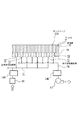
上記レジスト塗布現像処理装置は、図1に示すように、複数の被処理基板であるLCD用ガラス基板G(以下に基板Gという)を収容するカセットCを載置する搬入出部1と、基板Gにレジスト塗布及び現像を含む一連の処理を施すための複数の処理ユニットを備えた処理部2と、露光装置4との間で基板Gの受け渡しを行うためのインターフェイス部3とを具備しており、処理部2の両端にそれぞれ搬入出部1及びインターフェイス部3が配置されている。なお、図1において、レジスト塗布現像処理装置の長手方向をX方向、平面視においてX方向と直交する方向をY方向とする。
As shown in FIG. 1, the resist coating and developing apparatus includes a loading /
上記搬入出部1は、カセットCと処理部2との間で基板Gの搬入出を行うための搬送機構5を備えており、この搬入出部1において外部に対するカセットCの搬入出が行われる。また、搬送機構5は搬送アーム5aを有し、カセットCの配列方向であるY方向に沿って設けられた搬送路6上を移動可能であり、搬送アーム5aによりカセットCと処理部2との間で基板Gの搬入出が行われるように構成されている。
The loading /
上記処理部2は、基本的にX方向に伸びる基板G搬送用の平行な2列の搬送ラインA、Bを有しており、搬送ラインAに沿って搬入出部1側からインターフェイス部3に向けてスクラブ洗浄処理ユニット(SCR)11、第1の熱的処理ユニットセクション16、レジスト処理ユニット13及び第2の熱的処理ユニットセクション17が配列されている。また、搬送ラインBに沿ってインターフェイス部3側から搬入出部1に向けて第2の熱的処理ユニットセクション17、現像処理ユニット(DEV)14、i線UV照射ユニット(i−UV)15及び第3の熱的処理ユニット18が配列されている。なお、スクラブ洗浄処理ユニット(SCR)11の上の一部にはエキシマUV照射ユニット(e−UV)12が設けられている。この場合、エキシマUV照射ユニット(e−UV)12はスクラバ洗浄に先立って基板Gの有機物を除去するために設けられている。また、i線UV照射ユニット(i−UV)15は現像の脱色処理を行うために設けられる。
The processing unit 2 basically has two parallel rows of transport lines A and B for transporting the substrate G extending in the X direction. From the loading /
なお、第1の熱的処理ユニットセクション16は、基板Gに熱的処理を施す熱的処理ユニットが積層して構成された2つの熱的処理ユニットブロック(TB)31,32を有しており、熱的処理ユニットブロック(TB)31はスクラブ洗浄処理ユニット(SCR)11側に設けられ、熱的処理ユニットブロック(TB)32はレジスト処理ユニット13側に設けられている。これら2つの熱的処理ユニットブロック(TB)31,32の間に第1の搬送機構33が設けられている。
The first thermal
また、第2の熱的処理ユニットセクション17は、基板Gに熱的処理を施す熱的処理ユニットが積層して構成された2つの熱的処理ユニットブロック(TB)34,35を有しており、熱的処理ユニットブロック(TB)34はレジスト処理ユニット13側に設けられ、熱的処理ユニットブロック(TB)35は現像処理ユニット14側に設けられている。これら2つの熱的処理ユニットブロック(TB)34,35の間に第2の搬送機構36が設けられている。
The second thermal
また、第3の熱的処理ユニットセクション18は、基板Gに熱的処理を施す熱的処理ユニットが積層して構成された2つの熱的処理ユニットブロック(TB)37,38を有しており、熱的処理ユニットブロック(TB)37は現像処理ユニット(DEV)14側に設けられ、熱的処理ユニットブロック(TB)38はカセットステーション1側に設けられている。そして、これら2つの熱的処理ユニットブロック(TB)37,38の間に第3の搬送機構39が設けられている。
The third thermal
なお、インターフェイス部3には、エクステンション・クーリングステージ(EXT・COL)41と、周辺露光装置(EE)とタイトラ(TITLER)を積層して設けた外部装置ブロック42と、バッファーステージ(BUF)43及び第4の搬送機構44が配設されている。
The
このように構成されるインターフェイス部3において、第2の搬送機構36によって搬送される基板Gは、エクステンション・クーリングステージ(EXT・COL)41へ搬送され、第4の搬送機構44によって外部装置ブロック42の周辺露光装置(EE)に搬送されて、周辺レジスト除去のための露光が行われ、次いで、第4の搬送機構44により露光装置4に搬送されて、基板G上のレジスト膜が露光されて所定のパターンが形成される。場合によっては、バッファーステージ(BUF)43に基板Gを収容してから露光装置4に搬送される。そして、露光終了後、基板Gは第4の搬送機構44により外部装置ブロック42のタイトラ(TITLER)に搬入されて、基板Gに所定の情報が記された後、エクステンション・クーリングステージ(EXT・COL)41に載置され、再び処理部2に搬送されるように構成されている。
In the
上記レジスト処理ユニット13は、この発明に係る浮上式基板搬送処理装置を適用したレジスト塗布処理装置20と、このレジスト塗布処理装置20によって基板G上に形成されたレジスト膜を減圧容器(図示せず)内で減圧乾燥する減圧乾燥装置(VD)21とを具備している。
The resist
次に、この発明に係る浮上式基板搬送処理装置を適用したレジスト塗布処理装置20について説明する。
Next, a resist
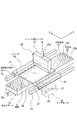
◎第1実施形態
図2は、上記レジスト塗布処理装置20の第1実施形態の要部を示す概略斜視図、図3は、レジスト塗布処理装置20における気体の供給及び吸引状態を示す概略構成図、図4及び図5は、気体の供給及び吸引状態を示す要部断面図である。
First Embodiment FIG. 2 is a schematic perspective view showing a main part of the first embodiment of the resist
上記レジスト塗布処理装置20は、表面から気体例えば空気を噴射及び吸引して基板Gを異なる高さに浮上する浮上ステージ22と、この浮上ステージ22の上方に配置され、基板Gの表面に処理液であるレジスト液Rを帯状に供給する処理液供給手段であるレジスト供給ノズル23と、基板Gの両側端をそれぞれ着脱可能に吸引保持する複数の基板保持部材24と、浮上ステージ22の両側に互いに平行に配置されるガイドレール25に沿ってスライダ26を移動する移動手段例えばリニアモータ28と、基板保持部材24とスライダ26とを連結すると共に、基板Gの浮上高さに追従して変位可能な連結手段27とで主に構成されている。
The resist
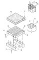
この場合、浮上ステージ22は、図2及び図6に示すように、図示しない搬送アームによって搬送される基板Gを受け取る昇降可能な複数例えば4本のリフトピン28aを具備する搬入領域22aと、レジスト供給ノズル23と基板Gとの隙間を一定の距離例えば100〜150μmに維持する塗布領域22bと、基板Gを受け渡す昇降可能な複数例えば4本のリフトピン28bを具備する搬出領域22cとが設けられている。
In this case, as shown in FIGS. 2 and 6, the
また、浮上ステージ22は、多数の気体供給孔(気体噴射孔)を有する例えばステンレスあるいはアルミニウム製の多孔質部材50にて形成されると共に、該多孔質部材50において気体供給孔を構成する多孔質部51と気密に区画される複数の吸引孔52を具備している。この場合、吸引孔52は多孔質部51に穿設された孔部52aの内面にコーティング52bを施すか(図4(b)参照)、あるいは、多孔質部51に穿設された孔部52a内に例えば合成樹脂製チューブ52cを嵌挿することによって形成されている(図4(c)参照)。また、複数の吸引孔52は基板Gの搬送方向(X方向)及び該搬送方向と直交する方向(Y方向)に対して傾斜状に配列されている。
The
また、塗布領域22bを代表して説明すると、多孔質部材50の多孔質部すなわち気体供給孔部には、多孔質部材50の下面に設けられた気体供給流路53と脈動を軽減するアキュムレータ54Aを介して気体供給手段例えばコンプレッサ55が接続され、吸引孔52には、多孔質部材50の下面に設けられた迂回流路56と脈動を軽減するアキュムレータ54Bを介して吸引手段である真空ポンプ57が接続されている(図3〜図5参照)。
Further, the
上記気体供給流路53と迂回流路56は、積層される複数(例えば5枚)の板部材(プレート)60a〜60eに設けられた孔部によって形成されている。この場合、迂回流路56は、図7に示すように、図4の紙面に対して直交する方向に適宜間隔をおいた複数(図面では3個の場合を示す)の孔部61aを有する第1のプレート60aと、孔部61aと同列に複数(図面では3×3=9個の場合を示す)の長孔部61bを有する第2のプレート60bと、孔部61a及び長孔部61bと同列に複数(図面では3×5=15個の場合を示す)の小孔部61cを有する第3のプレート60cと、第2のプレート60bの長孔部61bと列方向に若干ずれた位置に設けられる複数(9個)の長孔部61dを有する第4のプレート60dと、第1のプレート60aの孔部61aと対称位置に設けられる複数(3個)の孔部61eを有する第5のプレート60eを積層して、例えばボルトあるいは圧着等の固定手段で固定することによって形成されている。
The
上記のように構成される浮上ステージ22において、コンプレッサ55を駆動すると共に、真空ポンプ57を駆動することにより、空気が気体供給流路53を介して多孔質部材50の多孔質部51に形成される多数の気体供給孔により圧力損失を受けて分散されて上方に噴射すると共に、吸引孔52から迂回流路56を介して吸引される。これにより基板Gは浮上ステージ22上に浮上し、リニアモータ28の駆動によって搬入領域22aから塗布領域22bへ搬送されると共に、搬出領域22cに搬送される。この際、供給される空気は多孔質51部によって圧力損失を受けて分散され、吸引される空気は迂回流路56によって圧力損失を受けて供給(噴射)と吸引がバランスされるので、基板Gの浮上高さを均一にすることができると共に、浮上状態を安定させた状態で保持することができ、かつ、搬送中の基板Gの振動を抑制することができる。また、吸引孔52が基板Gの搬送方向(X方向)及び搬送方向と直交する方向(Y方向)に対して傾斜して配列されているので、基板Gの塗布膜にスジムラ(転写跡)が発生するのを抑制することができると共に、搬送中の基板Gの振動を更に確実に抑制することができる。すなわち、吸引孔52が基板Gの搬送方向(X方向)に対して傾斜して配列されることにより、基板Gの塗布膜にスジムラが発生するのを抑制することができる。つまり、複数の吸引孔52がX方向と同じであると、1つの直線上を複数の吸引孔52が通過するため、温度分布が異なってスジムラが生じるが、吸引孔52をX方向に対して傾斜して配列することにより、吸引孔52の軌跡が基板面内に分散するので、スジムラが起きにくい。また、吸引孔52の配列が基板Gの搬送方向と直交する方向(Y方向)に一致すると、基板Gの端部が一度に複数の吸引孔52にかかったり、逆に吸引孔52から外れるときに、基板端部が一度に複数の吸引孔52から外れて、基板Gの垂直方向(Z方向)の振動原因となる。これに対して、吸引孔52の配列をY方向に対して傾斜して配列することにより、このような問題を解決することができる。
In the
この場合、搬入領域22aと搬出領域22cにおいては、基板Gが約100〜150μmの高さの位置に浮上されている。また、塗布領域22bにおいては、基板Gが約50μmの高さの位置に浮上されている。なお、搬入領域22aと塗布領域22bとの間、及び塗布領域22bと搬出領域22cとの間には、それぞれ両者間の高さのギャップを繋げる繋ぎ領域22d,22eが設けられている。これら繋ぎ領域22d,22eにおいては、空気の噴射量及び吸引量を調整することによって基板Gを徐々に下降又は上昇するように構成されている。
In this case, in the carry-in
上記レジスト供給ノズル23は、浮上ステージ22の上方を跨ぐ門形フレーム(図示せず)に固定されており、図示しないレジストタンクに接続される供給管23aによって供給されるレジスト液Rを、基板Gの表面に帯状に供給(吐出,滴下)するように構成されている。
The resist
上記基板保持部材24は、基板Gの両側端をそれぞれ着脱可能に吸引保持する複数の図示しない吸着パッド及びバキューム管を具備しており、図示しない真空装置によって基板Gを着脱可能に保持し得るようになっている。
The
なお、上記連結手段27は、例えば基板保持部材24を構成する吸着パッドとスライダ26とを連結すると共に、基板Gの浮上高さに追従して変位可能な板ばね部材によって形成されている。この場合、板ばね部材は、基板保持部材24が基板Gを保持する保持力すなわち吸着パッドの吸着力より弱いばね力(弾撥力)を有するようにばね定数が設定されている。このように板ばね部材51のばね定数を設定することにより、基板保持部材24による基板Gの保持力(吸着力)を維持した状態で、基板Gの浮上高さに追従して基板保持部材24を変位することができる。なお、基板保持部材24は必ずしも吸着パッドで構成する必要はなく、例えば静電パッドにて構成してもよい。この静電パッドは、内部に設けた金属電極に電圧を印加し、基板Gと静電パッドの表面に正・負の電荷を発生させ、この間に働くジャンセン・ラーベック力によって基板Gを吸着保持するものである。また、連結手段27を、上記板ばね部材に代えて磁石体を用いてもよい。
The connecting means 27 is formed, for example, by a leaf spring member that connects the suction pad constituting the
次に、上記のように構成されるレジスト塗布処理装置20の動作態様について説明する。まず、熱的処理ユニット(TB)31によって熱処理された基板Gが図示しない搬送アームによって浮上ステージ22の搬入領域22a上に搬入されると、リフトピン28aが上昇して基板Gを受け取る。その後、搬送アームは浮上ステージ22上から外方へ退避する。基板Gを受け取った後、リフトピン28aは下降する一方、基板Gは搬入領域22aにおける浮上ステージ22の多孔質部51からの空気の供給(噴射)と、吸引孔52からの吸引とのバランスによって約100〜150μmの高さの位置に浮上され、この状態で、真空装置が作動して基板保持部材24の吸着パッド60によって基板Gが吸着保持される。この際、板ばね部材51が基板Gの浮上高さとスライダ26の高さとのギャップを吸収するので、基板Gは浮上ステージ22の搬入領域22a上の約100〜150μmの高さの位置に水平状態に維持される。
Next, the operation | movement aspect of the resist
次いで、リニアモータ28が駆動して基板Gが塗布領域22bに搬送される。塗布領域22bにおいては、浮上ステージ22の多孔質部51からの空気の供給(噴射)と、吸引孔52からの吸引とのバランスによって基板Gは約50μmの高さの位置に浮上される。この際、板ばね部材51が基板Gの浮上高さとスライダ26の高さとのギャップを吸収するので、基板Gは浮上ステージ22の塗布領域22b上の約50μmの高さの位置に水平状態に維持され、レジスト供給ノズル23との間に所定の隙間S(100〜150μm)を維持する。この状態で、レジスト供給ノズル23からレジスト液Rを帯状に供給(吐出)すると共に、基板Gを移動することによって、基板Gの表面にレジスト膜が均一に形成される。
Next, the
レジスト膜が形成された基板Gは搬出領域22cに移動されると、基板Gは搬出領域22cにおける浮上ステージ22の多孔質部51からの空気の供給(噴射)と、吸引孔52からの吸引とのバランスによって約100〜150μmの高さの位置に浮上され、この状態で、真空装置を停止して基板Gの吸着保持が解かれる。すると、リフトピン28bが上昇して基板Gを上方の受渡し位置へ移動する。この状態で、図示しない搬送アームが基板Gを受け取って基板Gを次工程の減圧乾燥装置(VD)21へ搬送する。
When the substrate G on which the resist film is formed is moved to the carry-out
◎第2実施形態
図8は、この発明に係る浮上式基板搬送処理装置の第2実施形態の要部を示す概略断面図、図9は、第2実施形態における気体(空気)の供給及び吸引部を示す要部分解斜視図(a)、(a)のII部を示す拡大斜視図(b)及びII部を示す別の拡大斜視図(c)である。
Second Embodiment FIG. 8 is a schematic cross-sectional view showing the main part of a second embodiment of the floating substrate transfer processing apparatus according to the present invention, and FIG. 9 shows the supply and suction of gas (air) in the second embodiment. They are a principal part disassembled perspective view which shows a part (a), an enlarged perspective view (b) which shows the II part of (a), and another enlarged perspective view (c) which shows the II part.
第2実施形態は、浮上ステージ22Aを、整列された多数の小孔71を有する多孔板70と、該多孔板70の下面に配設され、気体供給流路溝72と気体吸引流路溝73を交互に配列してなる流路プレート74とで構成し、気体供給流路溝72に供給管路75を介して気体供給手段であるコンプレッサ55を接続し、また、気体吸引流路溝73に吸引管路76を介して吸引手段である真空ポンプ57を接続した場合である。
In the second embodiment, the
なお、第2実施形態において、第1実施形態と同様に、供給管路75におけるコンプレッサ55の二次側(吐出側)にはアキュムレータ54Aが介設され、吸引管路76における真空ポンプ57の一次側(吸引側)にはアキュムレータ54Bが介設されている。なお、この場合、多孔板70は、例えば、図9(b)に示すように、多数のチューブ部材70a同士を集合接着させて形成することができる。また、例えば熱や薬品で溶解(消失)する線材をバインダで固め、後に線材を溶解(消失)することで、バインダが残って整列された多数の小孔71を有する多孔板70を作製することができる(図9(c)参照)。
In the second embodiment, as in the first embodiment, an
上記のように構成される第2実施形態の浮上式基板搬送処理装置において、気体供給流路溝72及び気体吸引流路溝73は交互に配列されていれば任意の配列でよいが、好ましくは、気体供給流路溝72及び気体吸引流路溝73を、基板Gの搬送方向(X方向)及び該搬送方向と直交する方向(Y方向)に対して傾斜状に配列するか(図10(a)参照)、又は、気体供給流路溝72及び気体吸引流路溝73を、X方向及びY方向に沿う波形状に形成するか(図10(b)参照)、あるいは、気体供給流路溝72及び気体吸引流路溝73を、それぞれY方向に延在する直状主溝72a,73aと、該直状主溝72a,73aに連なってX方向に延在する複数の枝溝72b,73bとで構成すると共に、隣接する気体供給流路溝72と気体吸引流路溝73の枝溝72b,73b同士をジグザグ状に配列する方がよい(図10(c)参照)。
In the floating substrate transfer processing apparatus of the second embodiment configured as described above, the gas supply
なお、第2実施形態において、その他の部分は第1実施形態と同じであるので、同一部分には同一符号を付して説明は省略する。 In the second embodiment, the other parts are the same as those in the first embodiment, so the same parts are denoted by the same reference numerals and description thereof is omitted.
上記のように構成される第2実施形態の浮上ステージ22Aにおいて、コンプレッサ55を駆動すると共に、真空ポンプ57を駆動することにより、空気が気体供給流路溝72を介して多孔板70に形成される多数の小孔71により圧力損失を受けて分散されて上方に噴射すると共に、多孔板70に形成される多数の小孔71から気体吸引流路溝73を介して吸引される。この際、供給される空気及び吸引される空気は多孔板70に形成された多数の小孔71によって圧力損失を受けて供給(噴射)と吸引がバランスされるので、基板Gの浮上高さを均一にすることができると共に、浮上状態を安定させた状態で保持することができ、かつ、搬送中の基板Gの振動を抑制することができる。
In the
また、気体吸引流路溝73を、X方向及びY方向に対して傾斜して配列するか(図10(a)参照)、又は、気体供給流路溝72及び気体吸引流路溝73を、X方向及びY方向に沿う波形状に形成するか(図10(b)参照)、あるいは、気体供給流路溝72及び気体吸引流路溝73を、それぞれY方向に延在する直状主溝72a,73aと、該直状主溝72a,73aに連なってX方向に延在する複数の枝溝72b,73bとで構成すると共に、隣接する気体供給流路溝72と気体吸引流路溝73の枝溝72b,73b同士をジグザグ状に配列する(図10(c)参照)ことにより、搬送中の基板Gの振動を更に確実に抑制することができる。
Further, the gas
◎第3実施形態
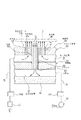
図11は、この発明に係る浮上式基板搬送処理装置の第3実施形態の要部を示す概略断面図、図12は、第3実施形態における気体(空気)の供給及び吸引部を示す要部分解斜視図である。
Third Embodiment FIG. 11 is a schematic cross-sectional view showing the main part of a third embodiment of the floating substrate transfer processing apparatus according to the present invention, and FIG. 12 shows the supply and suction of gas (air) in the third embodiment. It is a principal part disassembled perspective view which shows a part.
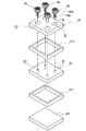
第3実施形態は、浮上ステージ22Bを、複数の大径孔81を設けた表面板80と、表面板80の下面との間に第1の空間91をおいて配設されると共に、大径孔81の直下に位置する小径孔83を設けた中間板82と、中間板82の下面との間に第2の空間92をおいて配設される下部板84とからなるステージ本体85と、整列された多数の小孔71を有し、小径孔83に気密に嵌合する多孔体86とで構成し、第1の空間91又は第2の空間92のいずれか一方、例えば第1の空間91に気体供給手段であるコンプレッサ55を接続すると共に、他方の空間例えば第2の空間92に吸引手段である真空ポンプ57を接続した場合である。この場合、表面板80と中間板82との間には、第1の空間91を構成する上部フレーム87aが介在されており、中間板82と下部板84との間には、第2の空間92を構成する下部フレーム87bが介在されている(図12参照)。
In the third embodiment, the
上記多孔体86は、図11及び図12に示すように、表面板80に設けられた大径孔81内に嵌合される大径頭部86aと、中間板82に設けられた小径孔83内にシール部材例えばOリング88を介して気密に嵌合する脚部86bとを有する断面略T字状に形成されている。なお、多孔体86の形状は必ずしも断面略T字状である必要はなく、例えば大径頭部86aの一端下部に脚部86bを垂下した断面略逆L字状に形成してもよい。
As shown in FIGS. 11 and 12, the
また、第1の空間91とコンプレッサ55を接続する供給管路75におけるコンプレッサ55の二次側(吐出側)にはアキュムレータ54Aが介設され、第2の空間92と真空ポンプ57を接続する吸引管路76における真空ポンプ57の一次側(吸引側)にはアキュムレータ54Bが介設されている。なお、この場合、多孔体86は、第2実施形態の多孔板70と同様に、多数のチューブ部材同士を集合接着させて形成することができる。また、例えば熱や薬品で溶解(消失)する線材をバインダで固め、後に線材を溶解(消失)させることによってバインダが残って整列された多数の小孔71を有する多孔体86を作製することができる。
In addition, an
なお、第3実施形態において、その他の部分は第1実施形態及び第2実施形態と同じであるので、同一部分には同一符号を付して説明は省略する。 In the third embodiment, the other parts are the same as those in the first embodiment and the second embodiment. Therefore, the same parts are denoted by the same reference numerals and description thereof is omitted.
上記のように構成される第3実施形態の浮上ステージ22Bにおいて、コンプレッサ55を駆動すると共に、真空ポンプ57を駆動することにより、空気が第1の空間91を介して多孔体86に形成される多数の小孔71により圧力損失を受けて分散されて上方に供給(噴射)すると共に、多孔体80に形成される多数の小孔71から第2の空間92を介して吸引される。この際、供給される空気及び吸引される空気は多孔板70に形成された多数の小孔71によって圧力損失を受けて供給(噴射)と吸引がバランスされるので、基板Gの浮上高さを均一にすることができると共に、浮上状態を安定させた状態で保持することができ、かつ、搬送中の基板Gの振動を抑制することができる。
In the
なお、上記説明では、第1の空間91にコンプレッサ55を接続し、第2の空間92に真空ポンプ57を接続する場合について説明したが、逆にしてもよい。すなわち、第1の空間91に真空ポンプ57を接続し、第2の空間92にコンプレッサ55を接続するようにしてもよい。
In the above description, the case where the
◎その他の実施形態
なお、上記実施形態では、この発明に係る浮上式基板搬送処理装置をレジスト塗布処理装置に適用した場合について説明したが、レジスト塗布処理装置以外の装置、例えば現像処理装置にも適用できることは勿論である。
Other Embodiments In the above embodiment, the case where the floating substrate transfer processing apparatus according to the present invention is applied to a resist coating processing apparatus has been described. However, the present invention also applies to apparatuses other than the resist coating processing apparatus, for example, development processing apparatuses. Of course, it can be applied.
G LCD用ガラス基板(被処理基板)
22,22A,22B 浮上ステージ
23 レジスト供給ノズル(処理液供給手段)
24 基板保持部材
28 リニアモータ(移動手段)
50 多孔質部材
51 多孔質部(気体供給孔)
52 吸引孔
55 コンプレッサ(気体供給手段)
56 迂回流路
57 真空ポンプ(吸引手段)
70 多孔板
71 小孔
72 気体供給流路溝
72a 直状主溝
72b 枝溝
73 気体吸引流路溝
73a 直状主溝
73b 枝溝
80 表面板
81 大径孔
82 中間板
83 小径孔
84 下部板
85 ステージ本体
86 多孔体
86a 大径頭部
86b 脚部
88 Oリング(シール部材)
91 第1の空間
92 第2の空間
G Glass substrate for LCD (substrate to be processed)
22, 22A,
24
50
52
56
70
91
Claims (4)
上記浮上ステージの上方に配置され、上記被処理基板の表面に処理液を供給する処理液供給手段と、
上記被処理基板の両側端をそれぞれ着脱可能に保持すると共に、被処理基板を上記浮上ステージ上で移動する移動手段と、を具備する浮上式基板搬送処理装置において、
上記浮上ステージを多孔質部材にて形成すると共に、該多孔質部材に気密に区画される複数の吸引孔を設け、
上記多孔質部材の多孔質部に気体供給手段を接続し、
上記吸引孔に迂回流路を介して吸引手段を接続し、
上記複数の吸引孔を被処理基板の搬送方向及び該搬送方向と直交する方向の直線上に一致しないよう傾斜状に配列する、ことを特徴とする浮上式基板搬送処理装置。 A levitation stage that levitates the substrate to be treated by jetting and sucking gas from the surface;
A processing liquid supply means that is disposed above the floating stage and supplies a processing liquid to the surface of the substrate to be processed;
In the floating substrate transfer processing apparatus comprising: a moving unit that detachably holds both side ends of the substrate to be processed and moves the substrate to be processed on the floating stage;
While forming the levitation stage with a porous member, provided a plurality of suction holes that are airtightly partitioned in the porous member,
Connecting a gas supply means to the porous portion of the porous member;
A suction means is connected to the suction hole via a bypass channel;
A floating substrate transfer processing apparatus, wherein the plurality of suction holes are arranged in an inclined manner so as not to coincide with a straight line in a transfer direction of a substrate to be processed and a direction orthogonal to the transfer direction.
上記浮上ステージの上方に配置され、上記被処理基板の表面に処理液を供給する処理液供給手段と、
上記被処理基板の両側端をそれぞれ着脱可能に保持すると共に、被処理基板を上記浮上ステージ上で移動する移動手段と、を具備する浮上式基板搬送処理装置において、
上記浮上ステージは、複数の大径孔を設けた表面板と、該表面板の下面との間に第1の空間をおいて配設されると共に、上記大径孔の直下に位置する小径孔を設けた中間板と、該中間板の下面との間に第2の空間をおいて配設される下部板とからなるステージ本体と、
整列された多数の小孔を有し、上記大径孔に嵌合する大径頭部の下部に上記小径孔に気密に嵌合する脚部を有する多孔体と、を具備し、
上記第1又は第2の空間のいずれか一方に気体供給手段を接続すると共に、他方の空間に吸引手段を接続してなる、ことを特徴とする浮上式基板搬送処理装置。 A levitation stage that levitates the substrate to be treated by jetting and sucking gas from the surface;
A processing liquid supply means that is disposed above the floating stage and supplies a processing liquid to the surface of the substrate to be processed;
In the floating substrate transfer processing apparatus comprising: a moving unit that detachably holds both side ends of the substrate to be processed and moves the substrate to be processed on the floating stage;
The levitation stage is provided with a first space between a surface plate provided with a plurality of large-diameter holes and a lower surface of the surface plate, and a small-diameter hole located immediately below the large-diameter hole. A stage body comprising an intermediate plate provided with a lower plate disposed with a second space between the lower surface of the intermediate plate;
A porous body having a large number of aligned small holes, and having a leg portion hermetically fitted to the small diameter hole at a lower portion of the large diameter head fitted to the large diameter hole;
A floating substrate transfer processing apparatus, wherein a gas supply unit is connected to one of the first and second spaces, and a suction unit is connected to the other space.
浮上ステージを形成する多孔質部材の多孔質部により圧力損失を受けて分散される気体を供給すると共に、多孔質部材に気密に区画される複数の吸引孔から圧力損失を与える迂回流路を介して吸引して、浮上ステージ上に被処理基板を浮上し、上記被処理基板の表面に処理液供給手段から処理液を帯状に供給すると共に、移動手段によって被処理基板を移動する、ことを特徴とする浮上式基板搬送処理方法。 A floating substrate transfer processing method using the floating substrate transfer processing apparatus according to claim 1 ,
Via a detour channel that supplies pressure loss from a plurality of suction holes that are airtightly partitioned into the porous member while supplying gas dispersed under pressure loss by the porous portion of the porous member forming the levitation stage Sucking and floating the substrate to be processed on the levitation stage, supplying the processing liquid to the surface of the substrate to be processed from the processing liquid supply unit in a strip shape, and moving the substrate to be processed by the moving unit. A floating substrate transfer processing method.
浮上ステージを形成する第1の空間又は第2の空間を介して多孔板の多数の小孔により圧力損失を受けて分散される気体を供給すると共に、多孔板の多数の小孔から上記第2の空間又は第1の空間を介して吸引して、浮上ステージ上に被処理基板を浮上し、上記被処理基板の表面に処理液供給手段から処理液を帯状に供給すると共に、移動手段によって被処理基板を移動する、ことを特徴とする浮上式基板搬送処理方法。 A floating substrate transfer processing method using the floating substrate transfer processing apparatus according to claim 2 ,
A gas dispersed by receiving a pressure loss by a large number of small holes in the perforated plate is supplied through the first space or the second space forming the levitation stage, and the second hole is supplied from the small holes in the perforated plate. The substrate to be processed is floated on the levitation stage, the processing liquid is supplied from the processing liquid supply unit to the surface of the substrate to be processed in a strip shape, and is moved by the moving unit. A floating substrate transfer processing method characterized by moving a processing substrate.
Priority Applications (5)
| Application Number | Priority Date | Filing Date | Title |
|---|---|---|---|
| JP2005208851A JP4553376B2 (en) | 2005-07-19 | 2005-07-19 | Floating substrate transfer processing apparatus and floating substrate transfer processing method |
| US11/486,005 US7905195B2 (en) | 2005-07-19 | 2006-07-14 | Floating-type substrate conveying and processing apparatus |
| TW095126266A TWI336113B (en) | 2005-07-19 | 2006-07-18 | Surfacing type substrate transportation processing apparatus and surfacing type substrate transportation processing method |
| TW099107296A TWI438857B (en) | 2005-07-19 | 2006-07-18 | Surfacing type substrate transportation processing apparatus and surfacing type substrate transportation processing method |
| KR1020060067297A KR101100486B1 (en) | 2005-07-19 | 2006-07-19 | Levitated substrate conveying treatment device |
Applications Claiming Priority (1)
| Application Number | Priority Date | Filing Date | Title |
|---|---|---|---|
| JP2005208851A JP4553376B2 (en) | 2005-07-19 | 2005-07-19 | Floating substrate transfer processing apparatus and floating substrate transfer processing method |
Publications (3)
| Publication Number | Publication Date |
|---|---|
| JP2007027495A JP2007027495A (en) | 2007-02-01 |
| JP2007027495A5 JP2007027495A5 (en) | 2007-07-05 |
| JP4553376B2 true JP4553376B2 (en) | 2010-09-29 |
Family
ID=37677905
Family Applications (1)
| Application Number | Title | Priority Date | Filing Date |
|---|---|---|---|
| JP2005208851A Active JP4553376B2 (en) | 2005-07-19 | 2005-07-19 | Floating substrate transfer processing apparatus and floating substrate transfer processing method |
Country Status (4)
| Country | Link |
|---|---|
| US (1) | US7905195B2 (en) |
| JP (1) | JP4553376B2 (en) |
| KR (1) | KR101100486B1 (en) |
| TW (2) | TWI438857B (en) |
Cited By (1)
| Publication number | Priority date | Publication date | Assignee | Title |
|---|---|---|---|---|
| CN110404717A (en) * | 2019-06-14 | 2019-11-05 | 上海维誉自动化设备有限公司 | A kind of automatic spraying coating line |
Families Citing this family (74)
| Publication number | Priority date | Publication date | Assignee | Title |
|---|---|---|---|---|
| WO2007105455A1 (en) * | 2006-02-28 | 2007-09-20 | Ulvac, Inc. | Stage device |
| JPWO2007145072A1 (en) * | 2006-06-14 | 2009-10-29 | 日本精工株式会社 | Support device |
| JP5047545B2 (en) * | 2006-06-30 | 2012-10-10 | 株式会社妙徳 | Levitation transport unit |
| JP4652351B2 (en) * | 2007-02-02 | 2011-03-16 | 大日本印刷株式会社 | Substrate support apparatus and substrate support method |
| JP4743716B2 (en) * | 2007-03-06 | 2011-08-10 | 東京エレクトロン株式会社 | Substrate processing equipment |
| JP4982292B2 (en) * | 2007-08-07 | 2012-07-25 | 東京応化工業株式会社 | Coating apparatus and coating method |
| JP5188759B2 (en) * | 2007-08-07 | 2013-04-24 | 東京応化工業株式会社 | Coating apparatus and coating method |
| JP2009043829A (en) * | 2007-08-07 | 2009-02-26 | Tokyo Ohka Kogyo Co Ltd | Coater and coating method |
| JP4942589B2 (en) * | 2007-08-30 | 2012-05-30 | 東京応化工業株式会社 | Coating apparatus and coating method |
| JP4384686B2 (en) * | 2007-09-25 | 2009-12-16 | 東京エレクトロン株式会社 | Normal pressure drying apparatus, substrate processing apparatus, and substrate processing method |
| JP4991495B2 (en) * | 2007-11-26 | 2012-08-01 | 東京エレクトロン株式会社 | Inspection holding member and manufacturing method of inspection holding member |
| JP5029486B2 (en) | 2008-05-13 | 2012-09-19 | 東京エレクトロン株式会社 | Coating apparatus, coating method, and storage medium |
| JP5012651B2 (en) | 2008-05-14 | 2012-08-29 | 東京エレクトロン株式会社 | Coating device, coating method, coating, developing device and storage medium |
| JP4857312B2 (en) * | 2008-07-16 | 2012-01-18 | シャープ株式会社 | Substrate transfer device |
| JP4972618B2 (en) * | 2008-08-05 | 2012-07-11 | シャープ株式会社 | Substrate transfer device |
| JP2010037082A (en) * | 2008-08-07 | 2010-02-18 | Sharp Corp | Substrate carrying device and substrate carrying method |
| KR101296659B1 (en) * | 2008-11-14 | 2013-08-14 | 엘지디스플레이 주식회사 | Washing device |
| US8699001B2 (en) * | 2009-08-20 | 2014-04-15 | Nikon Corporation | Object moving apparatus, object processing apparatus, exposure apparatus, object inspecting apparatus and device manufacturing method |
| US20110042874A1 (en) * | 2009-08-20 | 2011-02-24 | Nikon Corporation | Object processing apparatus, exposure apparatus and exposure method, and device manufacturing method |
| US20110053092A1 (en) * | 2009-08-20 | 2011-03-03 | Nikon Corporation | Object processing apparatus, exposure apparatus and exposure method, and device manufacturing method |
| KR101069600B1 (en) | 2009-09-01 | 2011-10-05 | 주식회사 케이씨텍 | Inline type substrate coater apparatus and method thereof |
| US9598247B2 (en) * | 2009-09-03 | 2017-03-21 | Game Changers, Llc | Method and apparatus for a dynamic air cushion transport system |
| JP4919115B2 (en) * | 2009-09-24 | 2012-04-18 | 横河電機株式会社 | Radiation inspection equipment |
| KR101158267B1 (en) * | 2009-10-26 | 2012-06-19 | 주식회사 나래나노텍 | A Floating Plate Being Used for A Substrate-Floating Unit, and A Substrate-Floating Unit, A Substrate-Transferring Device and A Coating Apparatus Having the Same |
| KR101141146B1 (en) * | 2009-12-30 | 2012-05-02 | 주식회사 케이씨텍 | Substrate transfer method |
| KR101099555B1 (en) * | 2010-01-12 | 2011-12-28 | 세메스 주식회사 | Apparatus for processing a substrate |
| US20110239231A1 (en) * | 2010-03-23 | 2011-09-29 | International Business Machines Corporation | Migrating electronic document version contents and version metadata as a collection with a single operation |
| JP5465595B2 (en) * | 2010-05-10 | 2014-04-09 | オイレス工業株式会社 | Non-contact transfer device |
| EP2388808A1 (en) * | 2010-05-20 | 2011-11-23 | Westfälische Wilhelms-Universität Münster | Contactless transport system |
| US8598538B2 (en) | 2010-09-07 | 2013-12-03 | Nikon Corporation | Movable body apparatus, object processing device, exposure apparatus, flat-panel display manufacturing method, and device manufacturing method |
| KR20140004113A (en) * | 2010-12-24 | 2014-01-10 | 오일레스고교 가부시키가이샤 | Upward flow forming element and noncontact transfer device using the upward flow forming element |
| JP5663297B2 (en) * | 2010-12-27 | 2015-02-04 | 東京応化工業株式会社 | Coating device |
| CN102543662B (en) * | 2010-12-30 | 2016-02-03 | 上海微电子装备有限公司 | The hot silicon chip heating system coiling and apply it |
| CN103298717B (en) * | 2011-01-14 | 2015-07-22 | 翁令司工业股份有限公司 | Non-contact transfer apparatus |
| US9136155B2 (en) * | 2011-11-17 | 2015-09-15 | Lam Research Ag | Method and device for processing wafer shaped articles |
| KR101312364B1 (en) * | 2011-12-22 | 2013-09-27 | 주식회사 나래나노텍 | Mounting and Removal Device and Method of Substrate, and Coating Apparatus and Method Having the Same |
| JP5912642B2 (en) * | 2012-02-20 | 2016-04-27 | 日本電気硝子株式会社 | Glass plate conveying apparatus and conveying method thereof |
| TWI527747B (en) * | 2012-02-28 | 2016-04-01 | 炭研軸封精工股份有限公司 | Non-contact adsorbing disk |
| KR101423822B1 (en) * | 2012-06-28 | 2014-07-28 | 세메스 주식회사 | Contactless chuck for transferring a wafer |
| JP5987528B2 (en) * | 2012-07-30 | 2016-09-07 | 株式会社タンケンシールセーコウ | Ascent equipment |
| KR101615869B1 (en) * | 2012-10-30 | 2016-04-26 | 닛산 지도우샤 가부시키가이샤 | Conveyor apparatus |
| JP2014218342A (en) * | 2013-05-09 | 2014-11-20 | オイレス工業株式会社 | Supporting air plate and gas flow resistor thereof |
| JP6226419B2 (en) * | 2013-08-22 | 2017-11-08 | オイレス工業株式会社 | Levitation transfer device |
| JP6339341B2 (en) * | 2013-10-11 | 2018-06-06 | 平田機工株式会社 | Processing system and processing method |
| JP6270114B2 (en) * | 2013-11-20 | 2018-01-31 | 東レエンジニアリング株式会社 | Substrate floating device |
| KR102059313B1 (en) * | 2014-04-30 | 2019-12-24 | 카티바, 인크. | Gas cushion apparatus and techniques for substrate coating |
| US10332770B2 (en) * | 2014-09-24 | 2019-06-25 | Sandisk Technologies Llc | Wafer transfer system |
| JP6949455B2 (en) | 2014-12-24 | 2021-10-13 | 株式会社タンケンシールセーコウ | Non-contact transfer device and non-contact suction plate |
| TWI735438B (en) * | 2015-03-30 | 2021-08-11 | 日商尼康股份有限公司 | Object carrier device, exposure apparatus, manufacturing method of flat panel display, device manufacturing method, object carrying method, and exposure method |
| CN113204177A (en) * | 2015-03-31 | 2021-08-03 | 株式会社尼康 | Exposure apparatus, method for manufacturing flat panel display, method for manufacturing device, and exposure method |
| JP6215281B2 (en) * | 2015-10-27 | 2017-10-18 | 株式会社日本製鋼所 | SUBSTRATE TRANSFER DEVICE, SEMICONDUCTOR MANUFACTURING DEVICE, AND SUBSTRATE TRANSFER METHOD |
| JP6651392B2 (en) * | 2016-03-22 | 2020-02-19 | 東レエンジニアリング株式会社 | Substrate floating transfer device |
| KR101690189B1 (en) * | 2016-03-23 | 2016-12-27 | (주) 세명유리 | Coating device for waterproof of mirror |
| FR3049941B1 (en) * | 2016-04-06 | 2018-04-13 | Saint- Gobain Glass France | CONVEYING AND HOLDING DEVICE FOR GLASS SHEET IN PARTICULAR IN A WASHING PLANT |
| US9633878B1 (en) * | 2016-04-21 | 2017-04-25 | Texas Instuments Incorporated | Conveyor apparatus and method for transporting leadframe |
| EP3472077A4 (en) * | 2016-06-21 | 2020-03-04 | Coreflow Ltd | Noncontact support platform with edge lifting |
| EP3480143A4 (en) * | 2016-06-30 | 2020-02-26 | Ace Machinery Co. Ltd. | Transport apparatus |
| WO2018001709A1 (en) * | 2016-07-01 | 2018-01-04 | Asml Netherlands B.V. | Stage system, lithographic apparatus, method for positioning and device manufacturing method |
| JP6854605B2 (en) * | 2016-08-29 | 2021-04-07 | 株式会社日本製鋼所 | Laser irradiation device, laser irradiation method, and manufacturing method of semiconductor device |
| JP6910518B2 (en) * | 2016-08-29 | 2021-07-28 | 株式会社日本製鋼所 | Laser irradiation device |
| JP6917691B2 (en) * | 2016-10-04 | 2021-08-11 | 株式会社日本製鋼所 | Laser irradiation device, laser irradiation method, and manufacturing method of semiconductor device |
| JP6819373B2 (en) * | 2017-03-10 | 2021-01-27 | 株式会社Ihi | Floating device and tension detector |
| US9889995B1 (en) * | 2017-03-15 | 2018-02-13 | Core Flow Ltd. | Noncontact support platform with blockage detection |
| JP6983578B2 (en) | 2017-08-25 | 2021-12-17 | 株式会社日本製鋼所 | Laser irradiation device, laser irradiation method, and manufacturing method of semiconductor device |
| US11660632B2 (en) * | 2018-03-28 | 2023-05-30 | Ecosys S.R.L. | Device for coating, in particular painting, the main surfaces of rigid panels with liquid products |
| JP7034817B2 (en) * | 2018-04-19 | 2022-03-14 | 株式会社日本製鋼所 | Manufacturing method of laser processing equipment and semiconductor equipment |
| JP7110005B2 (en) * | 2018-06-20 | 2022-08-01 | キヤノン株式会社 | Substrate rotation apparatus, substrate rotation method, lithographic apparatus, and article manufacturing method |
| CN109633939B (en) * | 2018-12-27 | 2024-04-16 | 苏州精濑光电有限公司 | LCD detection equipment |
| US20200266092A1 (en) * | 2019-02-19 | 2020-08-20 | Corning Incorporated | Apparatuses and methods for non-contact holding and measurement of thin substrates |
| JP7299790B2 (en) * | 2019-08-05 | 2023-06-28 | 東レエンジニアリング株式会社 | SUBSTRATE LIFTING TRANSPORT DEVICE AND SUBSTRATE POSITION CORRECTION METHOD OF SUBSTRATE LIFTING TRANSPORT DEVICE |
| KR102268617B1 (en) * | 2019-10-16 | 2021-06-23 | 세메스 주식회사 | Apparatus for processing substrate |
| CN113130368A (en) * | 2021-04-13 | 2021-07-16 | 南京中安半导体设备有限责任公司 | Air floatation chuck and wafer geometric parameter measuring device |
| JP7095166B2 (en) * | 2020-08-21 | 2022-07-04 | Jswアクティナシステム株式会社 | Laser irradiation device, laser irradiation method, and manufacturing method of semiconductor device |
| IT202100013085A1 (en) * | 2021-05-20 | 2022-11-20 | Cefla Soc Cooperativa | APPARATUS AND METHOD FOR PAINTING PANELS BY ROLLER, PREFERABLE PHOTOVOLTAIC PANELS |
Citations (9)
| Publication number | Priority date | Publication date | Assignee | Title |
|---|---|---|---|---|
| JP2000072251A (en) * | 1998-08-31 | 2000-03-07 | Watanabe Shoko:Kk | Flotation carrier device and flotation carrier system |
| JP2000128346A (en) * | 1998-08-20 | 2000-05-09 | Matsushita Electric Ind Co Ltd | Floating device, floating carrier and heat treatment device |
| JP2000159342A (en) * | 1998-11-20 | 2000-06-13 | Daiichi Shisetsu Kogyo Kk | Conveying apparatus for plate-shaped member |
| JP2004262608A (en) * | 2003-03-03 | 2004-09-24 | Orbotech Ltd | Air flotation device |
| JP2004273574A (en) * | 2003-03-05 | 2004-09-30 | Wakomu Denso:Kk | Substrate levitation equipment and method therefor |
| JP2004331265A (en) * | 2003-05-01 | 2004-11-25 | Olympus Corp | Floating unit and substrate inspection device |
| JP2004345744A (en) * | 2003-05-20 | 2004-12-09 | Hitachi Zosen Corp | Pneumatic floating device and pneumatic floating type carrier |
| JP2005132626A (en) * | 2003-10-06 | 2005-05-26 | Sumitomo Heavy Ind Ltd | Conveying apparatus, application system and inspection system |
| JP2006237097A (en) * | 2005-02-23 | 2006-09-07 | Tokyo Electron Ltd | Stage apparatus and application processing apparatus |
Family Cites Families (7)
| Publication number | Priority date | Publication date | Assignee | Title |
|---|---|---|---|---|
| DE69007733T2 (en) * | 1989-05-08 | 1994-09-29 | Philips Nv | DEVICE AND METHOD FOR TREATING A FLAT, DISC-SHAPED SUBSTRATE AT LOW PRESSURE. |
| DE59406900D1 (en) * | 1993-02-08 | 1998-10-22 | Sez Semiconduct Equip Zubehoer | Carrier for disc-shaped objects |
| JP3245813B2 (en) | 1996-11-27 | 2002-01-15 | 東京エレクトロン株式会社 | Coating film forming equipment |
| JP4398786B2 (en) | 2003-07-23 | 2010-01-13 | 東京エレクトロン株式会社 | Coating method and coating apparatus |
| JP4305918B2 (en) | 2004-01-30 | 2009-07-29 | 東京エレクトロン株式会社 | Floating substrate transfer processing equipment |
| KR101112029B1 (en) * | 2004-02-13 | 2012-03-21 | 에이에스엠 아메리카, 인코포레이티드 | Substrate Support System for Reduced Autodoping and Backside Deposition |
| US7604439B2 (en) * | 2004-04-14 | 2009-10-20 | Coreflow Scientific Solutions Ltd. | Non-contact support platforms for distance adjustment |
-
2005
- 2005-07-19 JP JP2005208851A patent/JP4553376B2/en active Active
-
2006
- 2006-07-14 US US11/486,005 patent/US7905195B2/en not_active Expired - Fee Related
- 2006-07-18 TW TW099107296A patent/TWI438857B/en active
- 2006-07-18 TW TW095126266A patent/TWI336113B/en not_active IP Right Cessation
- 2006-07-19 KR KR1020060067297A patent/KR101100486B1/en active IP Right Grant
Patent Citations (9)
| Publication number | Priority date | Publication date | Assignee | Title |
|---|---|---|---|---|
| JP2000128346A (en) * | 1998-08-20 | 2000-05-09 | Matsushita Electric Ind Co Ltd | Floating device, floating carrier and heat treatment device |
| JP2000072251A (en) * | 1998-08-31 | 2000-03-07 | Watanabe Shoko:Kk | Flotation carrier device and flotation carrier system |
| JP2000159342A (en) * | 1998-11-20 | 2000-06-13 | Daiichi Shisetsu Kogyo Kk | Conveying apparatus for plate-shaped member |
| JP2004262608A (en) * | 2003-03-03 | 2004-09-24 | Orbotech Ltd | Air flotation device |
| JP2004273574A (en) * | 2003-03-05 | 2004-09-30 | Wakomu Denso:Kk | Substrate levitation equipment and method therefor |
| JP2004331265A (en) * | 2003-05-01 | 2004-11-25 | Olympus Corp | Floating unit and substrate inspection device |
| JP2004345744A (en) * | 2003-05-20 | 2004-12-09 | Hitachi Zosen Corp | Pneumatic floating device and pneumatic floating type carrier |
| JP2005132626A (en) * | 2003-10-06 | 2005-05-26 | Sumitomo Heavy Ind Ltd | Conveying apparatus, application system and inspection system |
| JP2006237097A (en) * | 2005-02-23 | 2006-09-07 | Tokyo Electron Ltd | Stage apparatus and application processing apparatus |
Cited By (1)
| Publication number | Priority date | Publication date | Assignee | Title |
|---|---|---|---|---|
| CN110404717A (en) * | 2019-06-14 | 2019-11-05 | 上海维誉自动化设备有限公司 | A kind of automatic spraying coating line |
Also Published As
| Publication number | Publication date |
|---|---|
| KR101100486B1 (en) | 2011-12-29 |
| US7905195B2 (en) | 2011-03-15 |
| TW200731449A (en) | 2007-08-16 |
| KR20070011153A (en) | 2007-01-24 |
| TWI336113B (en) | 2011-01-11 |
| JP2007027495A (en) | 2007-02-01 |
| US20070017442A1 (en) | 2007-01-25 |
| TWI438857B (en) | 2014-05-21 |
| TW201025488A (en) | 2010-07-01 |
Similar Documents
| Publication | Publication Date | Title |
|---|---|---|
| JP4553376B2 (en) | Floating substrate transfer processing apparatus and floating substrate transfer processing method | |
| JP2007027495A5 (en) | ||
| JP4305918B2 (en) | Floating substrate transfer processing equipment | |
| JP4033841B2 (en) | Floating substrate transfer processing method and apparatus | |
| JP4554397B2 (en) | Stage device and coating treatment device | |
| JP4571525B2 (en) | Substrate processing apparatus and substrate processing method | |
| KR101087845B1 (en) | Coating processing apparatus and coating processing method | |
| JP2006237482A (en) | Substrate processing device, substrate processing method, and substrate processing program | |
| JP2006206324A (en) | Substrate carrying device | |
| JP4319175B2 (en) | Vacuum dryer | |
| JP2010098125A (en) | Apparatus and method for transporting substrate | |
| KR100837849B1 (en) | Processing solution supplying method and processing solution supplying apparatus | |
| TWI462215B (en) | Substrate processing apparatus, changing method and transferring method | |
| JP2009018917A (en) | Application device, substrate delivery method and application method | |
| KR20100035119A (en) | Reduced-pressure drying device and reduced-pressure drying method | |
| JP5221508B2 (en) | Substrate processing equipment | |
| JP2005247516A (en) | Levitated substrate conveying treatment device | |
| JP5165718B2 (en) | Substrate processing equipment | |
| KR101344926B1 (en) | Support unit, apparatus for treating substrate with the same | |
| JP6595276B2 (en) | Substrate processing apparatus and substrate processing method | |
| KR20180124891A (en) | Substrate floating carrier | |
| JP4386430B2 (en) | Coating film forming device | |
| JP2014013804A (en) | Coating processor, coating processing method, program and computer storage medium | |
| JP4327345B2 (en) | Liquid supply apparatus and liquid supply method | |
| TW200841414A (en) | Substrate conveyance system |
Legal Events
| Date | Code | Title | Description |
|---|---|---|---|
| A521 | Request for written amendment filed |
Free format text: JAPANESE INTERMEDIATE CODE: A523 Effective date: 20070517 |
|
| A621 | Written request for application examination |
Free format text: JAPANESE INTERMEDIATE CODE: A621 Effective date: 20070517 |
|
| A131 | Notification of reasons for refusal |
Free format text: JAPANESE INTERMEDIATE CODE: A131 Effective date: 20100107 |
|
| A521 | Request for written amendment filed |
Free format text: JAPANESE INTERMEDIATE CODE: A523 Effective date: 20100226 |
|
| A131 | Notification of reasons for refusal |
Free format text: JAPANESE INTERMEDIATE CODE: A131 Effective date: 20100510 |
|
| A521 | Request for written amendment filed |
Free format text: JAPANESE INTERMEDIATE CODE: A523 Effective date: 20100624 |
|
| TRDD | Decision of grant or rejection written | ||
| A01 | Written decision to grant a patent or to grant a registration (utility model) |
Free format text: JAPANESE INTERMEDIATE CODE: A01 Effective date: 20100712 |
|
| A01 | Written decision to grant a patent or to grant a registration (utility model) |
Free format text: JAPANESE INTERMEDIATE CODE: A01 |
|
| A61 | First payment of annual fees (during grant procedure) |
Free format text: JAPANESE INTERMEDIATE CODE: A61 Effective date: 20100712 |
|
| FPAY | Renewal fee payment (event date is renewal date of database) |
Free format text: PAYMENT UNTIL: 20130723 Year of fee payment: 3 |
|
| R150 | Certificate of patent or registration of utility model |
Ref document number: 4553376 Country of ref document: JP Free format text: JAPANESE INTERMEDIATE CODE: R150 Free format text: JAPANESE INTERMEDIATE CODE: R150 |
|
| R250 | Receipt of annual fees |
Free format text: JAPANESE INTERMEDIATE CODE: R250 |
|
| R250 | Receipt of annual fees |
Free format text: JAPANESE INTERMEDIATE CODE: R250 |
|
| R250 | Receipt of annual fees |
Free format text: JAPANESE INTERMEDIATE CODE: R250 |
|
| R250 | Receipt of annual fees |
Free format text: JAPANESE INTERMEDIATE CODE: R250 |
|
| R250 | Receipt of annual fees |
Free format text: JAPANESE INTERMEDIATE CODE: R250 |
|
| R250 | Receipt of annual fees |
Free format text: JAPANESE INTERMEDIATE CODE: R250 |
|
| R250 | Receipt of annual fees |
Free format text: JAPANESE INTERMEDIATE CODE: R250 |