JP4537285B2 - 走査線湾曲補正機構を有する光学走査装置 - Google Patents
走査線湾曲補正機構を有する光学走査装置 Download PDFInfo
- Publication number
- JP4537285B2 JP4537285B2 JP2005213310A JP2005213310A JP4537285B2 JP 4537285 B2 JP4537285 B2 JP 4537285B2 JP 2005213310 A JP2005213310 A JP 2005213310A JP 2005213310 A JP2005213310 A JP 2005213310A JP 4537285 B2 JP4537285 B2 JP 4537285B2
- Authority
- JP
- Japan
- Prior art keywords
- mirror
- pressing
- optical
- scanning line
- leaf spring
- Prior art date
- Legal status (The legal status is an assumption and is not a legal conclusion. Google has not performed a legal analysis and makes no representation as to the accuracy of the status listed.)
- Active
Links
Images


Classifications
-
- G—PHYSICS
- G02—OPTICS
- G02B—OPTICAL ELEMENTS, SYSTEMS OR APPARATUS
- G02B26/00—Optical devices or arrangements for the control of light using movable or deformable optical elements
- G02B26/08—Optical devices or arrangements for the control of light using movable or deformable optical elements for controlling the direction of light
- G02B26/10—Scanning systems
-
- G—PHYSICS
- G02—OPTICS
- G02B—OPTICAL ELEMENTS, SYSTEMS OR APPARATUS
- G02B27/00—Optical systems or apparatus not provided for by any of the groups G02B1/00 - G02B26/00, G02B30/00
- G02B27/62—Optical apparatus specially adapted for adjusting optical elements during the assembly of optical systems
-
- B—PERFORMING OPERATIONS; TRANSPORTING
- B41—PRINTING; LINING MACHINES; TYPEWRITERS; STAMPS
- B41J—TYPEWRITERS; SELECTIVE PRINTING MECHANISMS, i.e. MECHANISMS PRINTING OTHERWISE THAN FROM A FORME; CORRECTION OF TYPOGRAPHICAL ERRORS
- B41J2/00—Typewriters or selective printing mechanisms characterised by the printing or marking process for which they are designed
- B41J2/435—Typewriters or selective printing mechanisms characterised by the printing or marking process for which they are designed characterised by selective application of radiation to a printing material or impression-transfer material
- B41J2/44—Typewriters or selective printing mechanisms characterised by the printing or marking process for which they are designed characterised by selective application of radiation to a printing material or impression-transfer material using single radiation source per colour, e.g. lighting beams or shutter arrangements
-
- G—PHYSICS
- G02—OPTICS
- G02B—OPTICAL ELEMENTS, SYSTEMS OR APPARATUS
- G02B26/00—Optical devices or arrangements for the control of light using movable or deformable optical elements
- G02B26/08—Optical devices or arrangements for the control of light using movable or deformable optical elements for controlling the direction of light
- G02B26/0816—Optical devices or arrangements for the control of light using movable or deformable optical elements for controlling the direction of light by means of one or more reflecting elements
- G02B26/0825—Optical devices or arrangements for the control of light using movable or deformable optical elements for controlling the direction of light by means of one or more reflecting elements the reflecting element being a flexible sheet or membrane, e.g. for varying the focus
-
- G—PHYSICS
- G02—OPTICS
- G02B—OPTICAL ELEMENTS, SYSTEMS OR APPARATUS
- G02B26/00—Optical devices or arrangements for the control of light using movable or deformable optical elements
- G02B26/08—Optical devices or arrangements for the control of light using movable or deformable optical elements for controlling the direction of light
- G02B26/10—Scanning systems
- G02B26/12—Scanning systems using multifaceted mirrors
- G02B26/125—Details of the optical system between the polygonal mirror and the image plane
- G02B26/126—Details of the optical system between the polygonal mirror and the image plane including curved mirrors
Description
図を用いて本発明の第1実施形態について説明する。説明にあたり、画像形成装置の全体説明をした後、光学走査装置の詳細な構成について説明する。
まず、画像形成装置について説明する。本実施形態においては、複数の像担持体(感光体)を有するカラー画像形成装置について説明する。図8は画像形成装置の概略説明図である。
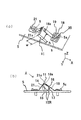
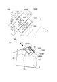
次に、光学走査装置1について詳細に説明する。図1は光学走査装置の斜視図である。図1及び図8に示すように、光学走査装置1は、感光体ドラム12の上方に一つの感光体ドラム12に対して一つずつ配設されている。
図2を用いて折り返しミラー11を支持する構成を詳細に説明する。図2は折り返しミラー11を光学箱5に取り付けた状態を説明する図である。図においては、折り返しミラー11の長手方向(主走査方向)の片側端部のみ図示しているが、反対側端部も同形状である。また、図2(a)は折り返しミラー11の一方の端部付近の斜視図、図2(b)は図2(a)のY方向矢視図である。
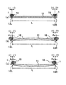
図3及び図4を用いて走査線の湾曲を補正する構成(走査線湾曲補正機構)を説明する。図3は、板バネ18の押圧位置を折り返しミラー11の長手方向に移動させた場合の、折り返しミラー11の変形の様子を示しており、図2を矢印A方向から見た模式図である。また図4は折り返しミラー11の変形の結果、感光体ドラム12上に生じる走査線がどのように変化するかを説明する図である。
図6を用いて本発明の第2実施形態について説明する。本実施形態の板バネ(押圧部材)31は、前述の実施形態の板バネと同様に、折り返しミラー11を左右のミラー支持部材13と対向する位置において固定するためのものである。また、板バネ31は、折り返しミラー11の長手方向(主走査方向)に移動可能であり、板バネ31を移動させて折り返しミラー11を湾曲させ、走査線22の湾曲を補正する。折り返しミラー11を支持する板バネ31について詳細に説明する。前述と同様の構成については同符号を付すことで説明を省略する。
図6を用いて折り返しミラー11を支持する構成を詳細に説明する。図6は折り返しミラー11を光学箱(筐体)42に取り付けた状態を説明する図である。図においては、折り返しミラー11の長手方向(主走査方向)の片側端部のみ図示しているが、反対側端部も同形状である。また、図6(a)は折り返しミラー11の一方の端部付近の斜視図、図6(b)は図6(a)のY方向矢視図、図6(c)は図6(a)のZ方向矢視図である。
図を用いて本発明の第3実施形態について説明する。本実施形態の板バネ(押圧部材)51は、前述の実施形態と同様に、折り返しミラー11を左右のミラー支持部材13と対向する位置において固定するためのものである。また、板バネ51は、折り返しミラー11の長手方向(主走査方向)に移動可能であり、板バネ51を移動させて折り返しミラー11を湾曲させ、走査線22の湾曲を補正する。折り返しミラー11を支持する板バネ51について詳細に説明する。前述と同様の構成については同符号を付すことで説明を省略する。
図7を用いて折り返しミラー11を支持する構成を詳細に説明する。図7は折り返しミラー11を光学箱(筐体)62に取り付けた状態を説明する図である。図においては、折り返しミラー11の長手方向(主走査方向)の片側端部のみ図示しているが、反対側端部も同形状である。また、図7(a)は折り返しミラー11の一方の端部付近の斜視図、図7(b)は図7(a)のY方向矢視図、図7(c)は図7(a)のZ方向矢視図である。
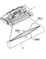
図11は実施形態4の光学走査装置の斜視図、図12(a)はミラー11の一方の端部付近に設けられた走査線湾曲補正機構100Rの斜視図、図12(b)は、図12(a)をY方向から見たときの断面図である。なお、前述の実施形態と同一の機能を有する部材には同じ番号を付してあり、再度の説明は省略する。また、走査線湾曲補正機構100Lの構造は100Rと同じである。
図14は第5実施形態の光学走査装置に設けられた走査線湾曲補正機構の断面図である。図14はミラーの長手方向一端部付近を示したものであり、他端部付近にも図14と同様の走査線湾曲補正機構があるが説明は省略する。本実施形態の走査線湾曲補正機構も、押圧部材による押圧点の位置(駒の位置)がミラー長手方向に関しミラー支持部材(台座)による支点の位置を越えて移動可能になっているが、この点に関しては実施形態1〜4と同様なので説明は省略する。
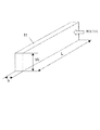
図15は第6実施形態の光学走査装置に設けられた走査線湾曲補正機構の斜視図である。図15はミラーの長手方向一端部付近を示したものであり、他端部付近にも図15と同様の走査線湾曲補正機構があるが説明は省略する。本実施形態の走査線湾曲補正機構も、押圧部材による押圧点の位置(駒の位置)がミラー長手方向に関しミラー支持部材(台座)による支点の位置を越えて移動可能になっているが、この点に関しても実施形態1〜5と同様なので説明は省略する。
Claims (8)
- 光源から出射するレーザ光を偏向する偏向器と、
前記偏向器によって偏向されたレーザ光を被走査面に導く光学素子と、
前記光学素子の長手方向端部付近を支持する支持部材と、前記光学素子を前記支持部材に向けて押圧する押圧部材とを備え、レーザ光によって被走査面に形成される走査線の湾曲を補正する湾曲補正機構と、を有し、
前記支持部材による支点は固定され、前記押圧部材による押圧点は前記光学素子の長手方向に移動可能である光学走査装置において、
前記押圧部材は、前記光学素子を押圧する力を付与するばね部と、前記ばね部に対してスライド可能に取り付けられ前記光学素子と接触する前記押圧点を備えた移動部と、を備え、
前記湾曲補正機構は、前記押圧部材が前記光学素子を押圧した状態で前記光学素子の長手方向に沿って前記移動部の押圧点をスライドさせることにより、前記支持部材の支持点と前記移動部の押圧点との間の前記光学素子の長手方向における距離を調整可能であることを特徴とする光学走査装置。 - 前記移動部の押圧点の位置は、前記光学素子の長手方向において、前記支持部材の支持点の位置を越えて移動可能であることを特徴とする請求項1に記載の光学走査装置。
- 前記押圧部材は、前記移動部の移動を案内する案内部を有することを特徴とする請求項1又は2に記載の光学走査装置。
- 前記ばね部と前記移動部は接着剤によって固定されていることを特徴とする請求項1乃至3のいずれか一項に記載の光学走査装置。
- 前記ばね部は前記移動部の移動を規制する移動規制機構を有することを特徴とする請求項1乃至3のいずれか一項に記載の光学走査装置。
- 前記偏向器と前記光学素子と前記湾曲補正機構を収容する光学箱を有し、前記支持部材は前記光学箱の一部であることを特徴とする請求項1乃至5のいずれか1項に記載の光学走査装置。
- 前記光学素子は、前記偏向器によって偏向されたレーザ光を被走査面へ反射するミラーであることを特徴とする請求項1乃至6のいずれか1項に記載の光学走査装置。
- 前記光学素子は、前記偏向器によって偏向されたレーザ光が透過するレンズであることを特徴とする請求項1乃至6のいずれか1項に記載の光学走査装置。
Priority Applications (4)
| Application Number | Priority Date | Filing Date | Title |
|---|---|---|---|
| JP2005213310A JP4537285B2 (ja) | 2004-07-29 | 2005-07-22 | 走査線湾曲補正機構を有する光学走査装置 |
| PCT/JP2005/014366 WO2006011683A1 (ja) | 2004-07-29 | 2005-07-29 | 走査線湾曲補正機構を有する光学走査装置 |
| KR1020077004617A KR100894951B1 (ko) | 2004-07-29 | 2005-07-29 | 주사선 만곡 보정 기구를 갖는 광학 주사 장치 |
| US11/319,099 US7453487B2 (en) | 2004-07-29 | 2005-12-28 | Optical scanning apparatus having scanning line curvature correcting mechanism with sliding pressure point along a longitudinal direction of the optical element |
Applications Claiming Priority (2)
| Application Number | Priority Date | Filing Date | Title |
|---|---|---|---|
| JP2004221598 | 2004-07-29 | ||
| JP2005213310A JP4537285B2 (ja) | 2004-07-29 | 2005-07-22 | 走査線湾曲補正機構を有する光学走査装置 |
Publications (3)
| Publication Number | Publication Date |
|---|---|
| JP2006065310A JP2006065310A (ja) | 2006-03-09 |
| JP2006065310A5 JP2006065310A5 (ja) | 2008-09-04 |
| JP4537285B2 true JP4537285B2 (ja) | 2010-09-01 |
Family
ID=35786407
Family Applications (1)
| Application Number | Title | Priority Date | Filing Date |
|---|---|---|---|
| JP2005213310A Active JP4537285B2 (ja) | 2004-07-29 | 2005-07-22 | 走査線湾曲補正機構を有する光学走査装置 |
Country Status (4)
| Country | Link |
|---|---|
| US (1) | US7453487B2 (ja) |
| JP (1) | JP4537285B2 (ja) |
| KR (1) | KR100894951B1 (ja) |
| WO (1) | WO2006011683A1 (ja) |
Families Citing this family (24)
| Publication number | Priority date | Publication date | Assignee | Title |
|---|---|---|---|---|
| JP5317409B2 (ja) | 2006-01-05 | 2013-10-16 | キヤノン株式会社 | 光学走査装置 |
| JP4875896B2 (ja) * | 2006-01-11 | 2012-02-15 | 株式会社リコー | 光走査装置及びこれを備える画像形成装置並びにレンズ位置調整方法 |
| JP4736935B2 (ja) * | 2006-04-28 | 2011-07-27 | ブラザー工業株式会社 | 走査光学装置 |
| JP4983156B2 (ja) * | 2006-08-29 | 2012-07-25 | 富士ゼロックス株式会社 | 画像形成装置 |
| JP5354323B2 (ja) * | 2007-07-02 | 2013-11-27 | 株式会社リコー | 光走査装置及び画像形成装置 |
| US8044988B2 (en) * | 2007-07-24 | 2011-10-25 | Lexmark International, Inc. | Spring Clip |
| JP5139784B2 (ja) * | 2007-12-04 | 2013-02-06 | キヤノン株式会社 | 画像形成装置 |
| JP5075616B2 (ja) * | 2007-12-27 | 2012-11-21 | 株式会社リコー | 画像形成装置 |
| JP5488960B2 (ja) * | 2009-06-17 | 2014-05-14 | 株式会社リコー | 湾曲補正機構、光走査装置、画像形成装置および光走査装置の製造方法 |
| JP5355253B2 (ja) * | 2009-06-30 | 2013-11-27 | キヤノン株式会社 | 光走査装置 |
| US8319813B2 (en) * | 2009-08-03 | 2012-11-27 | Lexmark International Inc. | Mounting assembly for reflection mirror in laser scanning unit |
| JP5284226B2 (ja) * | 2009-09-02 | 2013-09-11 | キヤノン株式会社 | 光走査装置およびそれを備える画像形成装置 |
| JP2011118161A (ja) * | 2009-12-03 | 2011-06-16 | Ricoh Co Ltd | 画像形成装置 |
| JP5437162B2 (ja) * | 2010-05-14 | 2014-03-12 | シャープ株式会社 | 光走査装置および画像形成装置 |
| JP5403432B2 (ja) | 2010-06-22 | 2014-01-29 | 株式会社リコー | 主走査線湾曲補正機構、光走査装置および画像形成装置 |
| JP5427831B2 (ja) * | 2010-11-25 | 2014-02-26 | 京セラドキュメントソリューションズ株式会社 | 光学部品取付構造及びそれを備えた画像読取装置及びそれを備えた画像形成装置 |
| US20120182368A1 (en) * | 2011-01-13 | 2012-07-19 | Toshiba Tec Kabushiki Kaisha | Optical scanning device and image forming apparatus |
| KR101873035B1 (ko) * | 2012-01-11 | 2018-07-02 | 에이치피프린팅코리아 주식회사 | 광주사장치 및 이를 채용한 화상형성장치 |
| JP6061510B2 (ja) * | 2012-06-14 | 2017-01-18 | シャープ株式会社 | 光走査装置、及びそれを備えた画像形成装置 |
| JP2014209161A (ja) * | 2012-09-07 | 2014-11-06 | 株式会社リコー | 光学装置、光走査装置及び画像形成装置 |
| JP5871834B2 (ja) * | 2013-01-31 | 2016-03-01 | 京セラドキュメントソリューションズ株式会社 | 光学部材の調整機構、光走査装置、画像形成装置 |
| JP6128988B2 (ja) * | 2013-06-26 | 2017-05-17 | キヤノン株式会社 | 光走査装置及び画像形成装置 |
| JP2015047861A (ja) * | 2013-09-05 | 2015-03-16 | 船井電機株式会社 | 画像形成装置 |
| US9362716B2 (en) * | 2014-09-19 | 2016-06-07 | Ipg Photonics Corporation | Crystal mount for laser application |
Citations (5)
| Publication number | Priority date | Publication date | Assignee | Title |
|---|---|---|---|---|
| JP2000131636A (ja) * | 1998-10-21 | 2000-05-12 | Canon Inc | 走査光学装置 |
| JP2001215434A (ja) * | 2000-02-01 | 2001-08-10 | Fuji Xerox Co Ltd | 光学走査装置 |
| JP2001228427A (ja) * | 2000-02-16 | 2001-08-24 | Fuji Xerox Co Ltd | 光走査装置及び画像形成装置 |
| JP2002182145A (ja) * | 2000-12-15 | 2002-06-26 | Ricoh Co Ltd | 光走査装置及びそれを搭載した画像形成装置 |
| JP2003270573A (ja) * | 2002-03-18 | 2003-09-25 | Fuji Xerox Co Ltd | 光走査装置及びそれを備えた画像形成装置 |
Family Cites Families (12)
| Publication number | Priority date | Publication date | Assignee | Title |
|---|---|---|---|---|
| US1489934A (en) * | 1922-04-24 | 1924-04-08 | Hildore C Eklund | Camera attachment |
| US5543829A (en) * | 1994-10-19 | 1996-08-06 | Xerox Corporation | Method and apparatus for adjusting the curvature of a folding mirror in a raster scanning system |
| JP3324302B2 (ja) | 1994-11-15 | 2002-09-17 | 富士ゼロックス株式会社 | 画像形成装置 |
| JPH10186257A (ja) | 1996-12-27 | 1998-07-14 | Fuji Xerox Co Ltd | レーザビーム走査装置 |
| JPH11231240A (ja) | 1998-02-19 | 1999-08-27 | Fuji Xerox Co Ltd | 光走査装置 |
| JP2000235290A (ja) | 1998-12-17 | 2000-08-29 | Fuji Xerox Co Ltd | 画像形成装置 |
| JP3709727B2 (ja) | 1998-12-18 | 2005-10-26 | 富士ゼロックス株式会社 | 光ビーム走査装置 |
| JP2000258713A (ja) | 1999-03-09 | 2000-09-22 | Fuji Xerox Co Ltd | 走査線湾曲補正方法及び光走査装置 |
| JP2001117040A (ja) | 1999-10-15 | 2001-04-27 | Fuji Xerox Co Ltd | 光学走査装置及び画像形成装置 |
| US6414805B1 (en) * | 1999-12-07 | 2002-07-02 | Chroma Technology Corp. | Reflected-light type fluorescence microscope and filter cassette used therefor |
| US6219082B1 (en) * | 1999-12-09 | 2001-04-17 | Xerox Corporation | Printer raster output scanning system with differential screw micron level bow correction |
| JP2003149575A (ja) * | 2001-11-09 | 2003-05-21 | Pentax Corp | 走査光学系 |
-
2005
- 2005-07-22 JP JP2005213310A patent/JP4537285B2/ja active Active
- 2005-07-29 KR KR1020077004617A patent/KR100894951B1/ko active IP Right Grant
- 2005-07-29 WO PCT/JP2005/014366 patent/WO2006011683A1/ja active Application Filing
- 2005-12-28 US US11/319,099 patent/US7453487B2/en active Active
Patent Citations (5)
| Publication number | Priority date | Publication date | Assignee | Title |
|---|---|---|---|---|
| JP2000131636A (ja) * | 1998-10-21 | 2000-05-12 | Canon Inc | 走査光学装置 |
| JP2001215434A (ja) * | 2000-02-01 | 2001-08-10 | Fuji Xerox Co Ltd | 光学走査装置 |
| JP2001228427A (ja) * | 2000-02-16 | 2001-08-24 | Fuji Xerox Co Ltd | 光走査装置及び画像形成装置 |
| JP2002182145A (ja) * | 2000-12-15 | 2002-06-26 | Ricoh Co Ltd | 光走査装置及びそれを搭載した画像形成装置 |
| JP2003270573A (ja) * | 2002-03-18 | 2003-09-25 | Fuji Xerox Co Ltd | 光走査装置及びそれを備えた画像形成装置 |
Also Published As
| Publication number | Publication date |
|---|---|
| WO2006011683A1 (ja) | 2006-02-02 |
| US7453487B2 (en) | 2008-11-18 |
| KR100894951B1 (ko) | 2009-04-27 |
| JP2006065310A (ja) | 2006-03-09 |
| KR20070044471A (ko) | 2007-04-27 |
| US20060103906A1 (en) | 2006-05-18 |
Similar Documents
| Publication | Publication Date | Title |
|---|---|---|
| JP4537285B2 (ja) | 走査線湾曲補正機構を有する光学走査装置 | |
| EP1792739B1 (en) | Optical scanning unit with fixing configuration for image forming apparatus | |
| JP4500738B2 (ja) | 光走査装置・画像形成装置 | |
| US7889409B2 (en) | Optical scanning device and image forming apparatus using the same | |
| US7505187B2 (en) | Optical scanning unit and image forming apparatus | |
| US8754919B2 (en) | Optical writing unit and image forming apparatus including same | |
| JP2006201626A (ja) | 光走査装置、画像形成装置および光走査装置の姿勢補正方法 | |
| US7557973B2 (en) | Optical scanning device and image forming apparatus provided with the same | |
| JP2004012596A (ja) | 光走査装置及び画像形成装置 | |
| US8004552B2 (en) | Optical scanning device and image forming apparatus | |
| JP4799138B2 (ja) | 光学部品固定機構、光走査装置、及び画像形成装置 | |
| JP5196733B2 (ja) | 光学走査装置 | |
| EP1762392B1 (en) | An image forming apparatus capable of producing a high-precision light beam | |
| JP5049674B2 (ja) | 光走査装置及び画像形成装置 | |
| JP2008233203A (ja) | 光走査装置、及び画像形成装置 | |
| US20090153934A1 (en) | Optical scanner and image forming apparatus | |
| JP3348138B2 (ja) | 光走査装置 | |
| JP2005134623A (ja) | 光走査装置および画像形成装置 | |
| JP6886319B2 (ja) | 光走査装置および前記光走査装置を備えた画像形成装置 | |
| JP4508996B2 (ja) | 光学ユニット、画像形成装置、及び光学部品ユニットの固定方法 | |
| JP2008076460A (ja) | 光走査装置と画像形成装置 | |
| JP2006150836A (ja) | 光書込装置及び画像形成装置 | |
| JP5041668B2 (ja) | 光走査装置および画像形成装置 | |
| JP2009014786A (ja) | 光走査装置 | |
| JP2005049468A (ja) | 光走査装置および画像形成装置 |
Legal Events
| Date | Code | Title | Description |
|---|---|---|---|
| RD02 | Notification of acceptance of power of attorney |
Free format text: JAPANESE INTERMEDIATE CODE: A7422 Effective date: 20080116 |
|
| A521 | Request for written amendment filed |
Free format text: JAPANESE INTERMEDIATE CODE: A523 Effective date: 20080718 |
|
| A621 | Written request for application examination |
Free format text: JAPANESE INTERMEDIATE CODE: A621 Effective date: 20080718 |
|
| A131 | Notification of reasons for refusal |
Free format text: JAPANESE INTERMEDIATE CODE: A131 Effective date: 20100330 |
|
| A521 | Request for written amendment filed |
Free format text: JAPANESE INTERMEDIATE CODE: A523 Effective date: 20100527 |
|
| TRDD | Decision of grant or rejection written | ||
| A01 | Written decision to grant a patent or to grant a registration (utility model) |
Free format text: JAPANESE INTERMEDIATE CODE: A01 Effective date: 20100615 |
|
| A01 | Written decision to grant a patent or to grant a registration (utility model) |
Free format text: JAPANESE INTERMEDIATE CODE: A01 |
|
| A61 | First payment of annual fees (during grant procedure) |
Free format text: JAPANESE INTERMEDIATE CODE: A61 Effective date: 20100617 |
|
| FPAY | Renewal fee payment (event date is renewal date of database) |
Free format text: PAYMENT UNTIL: 20130625 Year of fee payment: 3 |
|
| R150 | Certificate of patent or registration of utility model |
Ref document number: 4537285 Country of ref document: JP Free format text: JAPANESE INTERMEDIATE CODE: R150 Free format text: JAPANESE INTERMEDIATE CODE: R150 |