JP4472011B2 - 複数のチャックを用いる基板パターニング - Google Patents
複数のチャックを用いる基板パターニング Download PDFInfo
- Publication number
- JP4472011B2 JP4472011B2 JP2008551459A JP2008551459A JP4472011B2 JP 4472011 B2 JP4472011 B2 JP 4472011B2 JP 2008551459 A JP2008551459 A JP 2008551459A JP 2008551459 A JP2008551459 A JP 2008551459A JP 4472011 B2 JP4472011 B2 JP 4472011B2
- Authority
- JP
- Japan
- Prior art keywords
- substrate
- chuck
- mold assembly
- nanoimprint
- disposed
- Prior art date
- Legal status (The legal status is an assumption and is not a legal conclusion. Google has not performed a legal analysis and makes no representation as to the accuracy of the status listed.)
- Active
Links
- 239000000758 substrate Substances 0.000 title claims description 594
- 238000000059 patterning Methods 0.000 title claims description 38
- 238000000034 method Methods 0.000 claims description 67
- 239000000463 material Substances 0.000 claims description 56
- 238000012545 processing Methods 0.000 claims description 31
- 238000001127 nanoimprint lithography Methods 0.000 claims 2
- 239000002861 polymer material Substances 0.000 description 68
- 239000012530 fluid Substances 0.000 description 43
- 238000001459 lithography Methods 0.000 description 32
- 230000008569 process Effects 0.000 description 24
- 238000012546 transfer Methods 0.000 description 10
- 230000005855 radiation Effects 0.000 description 9
- 230000009467 reduction Effects 0.000 description 4
- 238000004132 cross linking Methods 0.000 description 3
- 230000008020 evaporation Effects 0.000 description 3
- 238000001704 evaporation Methods 0.000 description 3
- 239000007788 liquid Substances 0.000 description 3
- 238000004519 manufacturing process Methods 0.000 description 3
- VYPSYNLAJGMNEJ-UHFFFAOYSA-N Silicium dioxide Chemical compound O=[Si]=O VYPSYNLAJGMNEJ-UHFFFAOYSA-N 0.000 description 2
- 238000004891 communication Methods 0.000 description 2
- 239000012636 effector Substances 0.000 description 2
- 229910052734 helium Inorganic materials 0.000 description 2
- 239000001307 helium Substances 0.000 description 2
- SWQJXJOGLNCZEY-UHFFFAOYSA-N helium atom Chemical compound [He] SWQJXJOGLNCZEY-UHFFFAOYSA-N 0.000 description 2
- 238000005457 optimization Methods 0.000 description 2
- 241000282373 Panthera pardus Species 0.000 description 1
- -1 but not limited to Substances 0.000 description 1
- 238000012937 correction Methods 0.000 description 1
- 230000008878 coupling Effects 0.000 description 1
- 238000010168 coupling process Methods 0.000 description 1
- 238000005859 coupling reaction Methods 0.000 description 1
- 238000000151 deposition Methods 0.000 description 1
- 230000008021 deposition Effects 0.000 description 1
- 238000011161 development Methods 0.000 description 1
- 238000003618 dip coating Methods 0.000 description 1
- KPUWHANPEXNPJT-UHFFFAOYSA-N disiloxane Chemical class [SiH3]O[SiH3] KPUWHANPEXNPJT-UHFFFAOYSA-N 0.000 description 1
- 238000000203 droplet dispensing Methods 0.000 description 1
- 238000005516 engineering process Methods 0.000 description 1
- 230000007613 environmental effect Effects 0.000 description 1
- 239000010408 film Substances 0.000 description 1
- 229920002313 fluoropolymer Polymers 0.000 description 1
- 239000005350 fused silica glass Substances 0.000 description 1
- 238000005259 measurement Methods 0.000 description 1
- 229910052751 metal Inorganic materials 0.000 description 1
- 239000002184 metal Substances 0.000 description 1
- 150000002739 metals Chemical class 0.000 description 1
- 238000012986 modification Methods 0.000 description 1
- 230000004048 modification Effects 0.000 description 1
- 230000003287 optical effect Effects 0.000 description 1
- 229920000620 organic polymer Polymers 0.000 description 1
- 229920000642 polymer Polymers 0.000 description 1
- 238000004886 process control Methods 0.000 description 1
- 239000010453 quartz Substances 0.000 description 1
- 238000002310 reflectometry Methods 0.000 description 1
- 229910052594 sapphire Inorganic materials 0.000 description 1
- 239000010980 sapphire Substances 0.000 description 1
- 229920006395 saturated elastomer Polymers 0.000 description 1
- 239000004065 semiconductor Substances 0.000 description 1
- 239000005368 silicate glass Substances 0.000 description 1
- 229910052710 silicon Inorganic materials 0.000 description 1
- 239000010703 silicon Substances 0.000 description 1
- 238000007711 solidification Methods 0.000 description 1
- 230000008023 solidification Effects 0.000 description 1
- 238000004528 spin coating Methods 0.000 description 1
- 238000000427 thin-film deposition Methods 0.000 description 1
- 230000032258 transport Effects 0.000 description 1
Images


Classifications
-
- G—PHYSICS
- G03—PHOTOGRAPHY; CINEMATOGRAPHY; ANALOGOUS TECHNIQUES USING WAVES OTHER THAN OPTICAL WAVES; ELECTROGRAPHY; HOLOGRAPHY
- G03F—PHOTOMECHANICAL PRODUCTION OF TEXTURED OR PATTERNED SURFACES, e.g. FOR PRINTING, FOR PROCESSING OF SEMICONDUCTOR DEVICES; MATERIALS THEREFOR; ORIGINALS THEREFOR; APPARATUS SPECIALLY ADAPTED THEREFOR
- G03F7/00—Photomechanical, e.g. photolithographic, production of textured or patterned surfaces, e.g. printing surfaces; Materials therefor, e.g. comprising photoresists; Apparatus specially adapted therefor
- G03F7/0002—Lithographic processes using patterning methods other than those involving the exposure to radiation, e.g. by stamping
-
- B—PERFORMING OPERATIONS; TRANSPORTING
- B29—WORKING OF PLASTICS; WORKING OF SUBSTANCES IN A PLASTIC STATE IN GENERAL
- B29C—SHAPING OR JOINING OF PLASTICS; SHAPING OF MATERIAL IN A PLASTIC STATE, NOT OTHERWISE PROVIDED FOR; AFTER-TREATMENT OF THE SHAPED PRODUCTS, e.g. REPAIRING
- B29C59/00—Surface shaping of articles, e.g. embossing; Apparatus therefor
- B29C59/02—Surface shaping of articles, e.g. embossing; Apparatus therefor by mechanical means, e.g. pressing
- B29C59/022—Surface shaping of articles, e.g. embossing; Apparatus therefor by mechanical means, e.g. pressing characterised by the disposition or the configuration, e.g. dimensions, of the embossments or the shaping tools therefor
-
- B—PERFORMING OPERATIONS; TRANSPORTING
- B82—NANOTECHNOLOGY
- B82Y—SPECIFIC USES OR APPLICATIONS OF NANOSTRUCTURES; MEASUREMENT OR ANALYSIS OF NANOSTRUCTURES; MANUFACTURE OR TREATMENT OF NANOSTRUCTURES
- B82Y10/00—Nanotechnology for information processing, storage or transmission, e.g. quantum computing or single electron logic
-
- B—PERFORMING OPERATIONS; TRANSPORTING
- B82—NANOTECHNOLOGY
- B82Y—SPECIFIC USES OR APPLICATIONS OF NANOSTRUCTURES; MEASUREMENT OR ANALYSIS OF NANOSTRUCTURES; MANUFACTURE OR TREATMENT OF NANOSTRUCTURES
- B82Y40/00—Manufacture or treatment of nanostructures
-
- H—ELECTRICITY
- H01—ELECTRIC ELEMENTS
- H01L—SEMICONDUCTOR DEVICES NOT COVERED BY CLASS H10
- H01L21/00—Processes or apparatus adapted for the manufacture or treatment of semiconductor or solid state devices or of parts thereof
- H01L21/67—Apparatus specially adapted for handling semiconductor or electric solid state devices during manufacture or treatment thereof; Apparatus specially adapted for handling wafers during manufacture or treatment of semiconductor or electric solid state devices or components ; Apparatus not specifically provided for elsewhere
- H01L21/683—Apparatus specially adapted for handling semiconductor or electric solid state devices during manufacture or treatment thereof; Apparatus specially adapted for handling wafers during manufacture or treatment of semiconductor or electric solid state devices or components ; Apparatus not specifically provided for elsewhere for supporting or gripping
- H01L21/687—Apparatus specially adapted for handling semiconductor or electric solid state devices during manufacture or treatment thereof; Apparatus specially adapted for handling wafers during manufacture or treatment of semiconductor or electric solid state devices or components ; Apparatus not specifically provided for elsewhere for supporting or gripping using mechanical means, e.g. chucks, clamps or pinches
-
- Y—GENERAL TAGGING OF NEW TECHNOLOGICAL DEVELOPMENTS; GENERAL TAGGING OF CROSS-SECTIONAL TECHNOLOGIES SPANNING OVER SEVERAL SECTIONS OF THE IPC; TECHNICAL SUBJECTS COVERED BY FORMER USPC CROSS-REFERENCE ART COLLECTIONS [XRACs] AND DIGESTS
- Y10—TECHNICAL SUBJECTS COVERED BY FORMER USPC
- Y10S—TECHNICAL SUBJECTS COVERED BY FORMER USPC CROSS-REFERENCE ART COLLECTIONS [XRACs] AND DIGESTS
- Y10S977/00—Nanotechnology
- Y10S977/84—Manufacture, treatment, or detection of nanostructure
- Y10S977/887—Nanoimprint lithography, i.e. nanostamp
Landscapes
- Engineering & Computer Science (AREA)
- Chemical & Material Sciences (AREA)
- Nanotechnology (AREA)
- Physics & Mathematics (AREA)
- General Physics & Mathematics (AREA)
- Crystallography & Structural Chemistry (AREA)
- Condensed Matter Physics & Semiconductors (AREA)
- Manufacturing & Machinery (AREA)
- Theoretical Computer Science (AREA)
- Mathematical Physics (AREA)
- Computer Hardware Design (AREA)
- Microelectronics & Electronic Packaging (AREA)
- Power Engineering (AREA)
- Mechanical Engineering (AREA)
- Shaping Of Tube Ends By Bending Or Straightening (AREA)
- Exposure Of Semiconductors, Excluding Electron Or Ion Beam Exposure (AREA)
- Manufacturing Of Magnetic Record Carriers (AREA)
Description
本出願は、すべて参照によって本明細書に組み込まれる、名称「Apparatus for and Methods for Nano−Imprinting with Multi−Substrate Chucks」の2006年1月20日に出願された米国特許仮出願第60/760738号、名称「Apparatus and Method for Nano−Imprinting with Multi−Substrate Chucks」の2006年9月27日に出願された米国特許仮出願第60/827125号、及び名称「Apparatus For and Methods For Imprinting,Aligning and Separation for Double Side Imprinting」の2005年12月8日に出願された米国特許仮出願第60/748430号の優先権を主張する、名称「Method and System for Double−Sided Patterning of Substrates」の2006年11月30日に出願された米国特許出願第11/565350号の一部継続出願である、名称「Residual Layer Thickness Measurement and Correction」の2006年4月3日に出願された米国特許仮出願第60/788808号の優先権を主張する。
Claims (21)
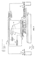
- ナノインプリント・リソグラフィ・システムにおいて第1と第2の基板をパターニングする方法であって、
空洞と、ナノインプリント・モールド・アセンブリに向かって配置される前記第1の基板の第1側面と、第1の基板チャックに向かって配置される前記第1の基板の第2側面を有する前記第1の基板チャック上に前記第1の基板を配置するステップと、
前記第1の基板の前記第1側面上にナノインプリント材料を配置するステップと、
前記第1の基板とナノインプリント・モールド・アセンブリ間の空間関係を取得して、第2の基板チャック上に前記第2の基板を配置するのと同時に、前記ナノインプリント・モールド・アセンブリを用いて、前記第1の基板の前記第1の側面上の前記ナノインプリント材料内にパターンをインプリントするステップと、
前記ナノインプリント・モールド・アセンブリを前記第1の基板上の前記ナノインプリント材料から分離するステップと、
前記第2の基板上にナノインプリント材料を配置するステップと、
前記第2の基板と前記ナノインプリント・モールド・アセンブリ間の空間関係を取得するのと同時に、前記第1の基板を前記第1の基板チャックから取り外し、かつ前記ナノインプリント・モールド・アセンブリを用いて前記第2の基板上の前記ナノインプリント材料内にパターンをインプリントするステップと、
前記ナノインプリント・モールド・アセンブリを前記第2の基板上の前記ナノインプリント材料から分離するステップであって、前記第1と第2の基板は、実質的に同じ処理条件を受ける、ステップと、
から構成され、
前記前記第1の基板を前記第1の基板チャックから取り外すステップは、前記ナノインプリント・モールド・アセンブリに対して前記第1の基板を180度フリッピングするステップをさらに含み、前記第1の基板上のナノインプリント材料が前記第1の基板チャックの前記空洞内に配置されるようにすることを特徴とする方法。 - 前記第2の基板チャックから前記第2の基板を取り外すステップをさらに含むことを特徴とする請求項1に記載の方法。
- 前記第2の基板を取り外す前記ステップは、前記ナノインプリント・モールド・アセンブリに対して前記第2の基板を180度フリッピングするステップをさらに含むことを特徴とする請求項2に記載の方法。
- 前記第1の基板を配置する前記ステップは、第3の基板と前記ナノインプリント・モールド・アセンブリ間の空間関係を取得し、かつ前記第2の基板チャック上に配置された前記第3の基板上のナノインプリント材料にパターンを形成するステップをさらに含むことを特徴とする請求項1に記載の方法。
- 前記第1の基板と前記ナノインプリント・モールド・アセンブリとの間の空間関係を取得する前記ステップは、同時に第3の基板を前記第2の基板チャックから取り外すステップをさらに含むことを特徴とする請求項1に記載の方法。
- 前記第1の基板を前記第1の基板チャックから取り外す前記ステップは、同時に第3の基板を前記第1の基板チャック上に配置するステップをさらに含むことを特徴とする請求項1に記載の方法。
- 前記第1と第2の基板に平行な軸の周りで前記第1と第2の基板チャックを並進させるステップをさらに含むことを特徴とする請求項1に記載の方法。
- 前記第1と第2の基板に垂直な軸の周りで前記第1と第2の基板チャックを回転させるステップをさらに含むことを特徴とする請求項1に記載の方法。
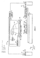
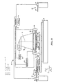
- ナノインプリント・リソグラフィ・システムにおける第1と第2の基板を処理する方法であって、
空洞を有する第1の基板チャックとナノインプリント・モールド・アセンブリ間の第1の空間関係、および前記第1の空間関係とは異なる、第2の基板チャックと前記ナノインプリント・モールド・アセンブリ間の第2の空間関係を取得して、前記第2の基板と前記第2の基板チャックと間に所望の空間関係を取得する間に、前記ナノインプリント・モールド・アセンブリを用いて、パターンが前記第1の基板チャック上に配置された前記第1の基板上のナノインプリント材料にインプリントされるようにするステップと、
前記第1の基板上の前記ナノプリント材料から前記ナノインプリント・モールド・アセンブリを分離するステップと、
前記ナノインプリント・モールド・アセンブリに対して、前記第1の基板を180度フリッピングして、前記第1の基板が前記第1の基板チャックの前記空洞内に配置されるようにするステップと、
から構成されることを特徴とする方法。 - 前記第1と第2の基板は、実質的に同じ処理条件を受けることを特徴とする請求項9に記載の方法。
- 前記第2の基板と前記第2の基板チャックとの間に所望の空間関係を取得する前記ステップは、前記第2の基板を前記第2の基板チャック上に配置するステップをさらに含むことを特徴とする請求項9に記載の方法。
- 前記第2の基板と前記第2の基板チャックとの間に所望の空間関係を取得する前記ステップは、前記第2の基板を前記第2の基板チャック上に配置されることから取り外すステップをさらに含むことを特徴とする請求項9に記載の方法。
- 前記第2の基板を取り外す前記ステップは、前記ナノインプリント・モールド・アセンブリに対して前記第2の基板を180度フリッピングするステップをさらに含むことを特徴とする請求項12に記載の方法。
- 前記第1の基板を前記第1の基板チャック上に配置するステップをさらに含むことを特徴とする請求項9に記載の方法。
- 前記第1の基板上に前記ナノインプリント材料を配置するステップをさらに含むことを特徴とする請求項9に記載の方法。
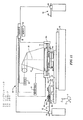
- 第1と第2の基板をパターニングする方法であって、
空洞と、モールド・アセンブリに向かって配置される前記第1の基板の第1側面と、前記第1の基板チャックに向かって配置された前記第1の基板の第2側面を有する第1の基板チャック上に前記第1の基板を配置するステップと、
前記第1の基板上に材料を配置するステップと、
前記第1の基板と前記モールド・アセンブリとの間の空間関係を取得し、第2の基板チャック上に前記第2の基板を配置するのと同時に、前記モールド・アセンブリを用いて、前記第1の基板上の前記材料内にパターンを形成するステップと、
前記モールド・アセンブリを前記第1の基板上の前記材料から分離するステップと、
前記第2の基板上に材料を配置するステップと、
前記第2の基板と前記モールド・アセンブリとの間の空間関係を取得するのと同時に、前記第1の基板を前記第1の基板チャックから取り外し、前記モールド・アセンブリを用いて、前記第2の基板上の前記材料内にパターンを形成するステップであって、前記第1の基板を取り外すステップは、前記プリント・モールド・アセンブリに対して前記第1の基板を180度フリッピングして、前記第1の基板上の材料が前記第1の基板チャックの前記空洞内に配置されるようにするステップと、
前記モールド・アセンブリを、前記第2の基板上の前記材料から分離するステップと、を含み、
前記第1と第2の基板は実質的に同じ処理条件を受けることを特徴とする方法。 - 前記第2の基板を前記第2の基板チャックから取り外すステップをさらに含むことを特徴とする請求項16に記載の方法。
- 前記第2の基板を取り外す前記ステップは、前記モールド・アセンブリに対して前記第2の基板を180度フリッピングするステップをさらに含むことを特徴とする請求項17に記載の方法。
- 前記第1の基板を配置する前記ステップは、第3の基板と前記モールド・アセンブリ間の空間関係を取得し、前記第2の基板チャック上に配置された前記第3の基板上の材料内にパターンを形成するステップをさらに含むことを特徴とする請求項16に記載の方法。
- 前記第1の基板と前記モールド・アセンブリ間の空間関係を取得する前記ステップは、同時に第3の基板を前記第2の基板チャックから取り外すステップをさらに含むことを特徴とする請求項16に記載の方法。
- 前記第1の基板を前記第1の基板チャックから取り外す前記ステップは、同時に第3の基板を前記第1の基板チャック上に配置するステップをさらに含むことを特徴とする請求項16に記載の方法。
Applications Claiming Priority (5)
| Application Number | Priority Date | Filing Date | Title |
|---|---|---|---|
| US76073806P | 2006-01-20 | 2006-01-20 | |
| US78880806P | 2006-04-03 | 2006-04-03 | |
| US82712506P | 2006-09-27 | 2006-09-27 | |
| US11/565,350 US7670529B2 (en) | 2005-12-08 | 2006-11-30 | Method and system for double-sided patterning of substrates |
| PCT/US2007/001670 WO2007084774A2 (en) | 2006-01-20 | 2007-01-20 | Patterning substrates employing multiple chucks |
Publications (3)
| Publication Number | Publication Date |
|---|---|
| JP2009524249A JP2009524249A (ja) | 2009-06-25 |
| JP2009524249A5 JP2009524249A5 (ja) | 2010-03-04 |
| JP4472011B2 true JP4472011B2 (ja) | 2010-06-02 |
Family
ID=38284757
Family Applications (1)
| Application Number | Title | Priority Date | Filing Date |
|---|---|---|---|
| JP2008551459A Active JP4472011B2 (ja) | 2006-01-20 | 2007-01-20 | 複数のチャックを用いる基板パターニング |
Country Status (6)
| Country | Link |
|---|---|
| US (2) | US7670530B2 (ja) |
| EP (1) | EP1973719A4 (ja) |
| JP (1) | JP4472011B2 (ja) |
| KR (1) | KR101324544B1 (ja) |
| TW (1) | TWI341935B (ja) |
| WO (1) | WO2007084774A2 (ja) |
Families Citing this family (78)
| Publication number | Priority date | Publication date | Assignee | Title |
|---|---|---|---|---|
| US7162035B1 (en) | 2000-05-24 | 2007-01-09 | Tracer Detection Technology Corp. | Authentication method and system |
| US7019819B2 (en) | 2002-11-13 | 2006-03-28 | Molecular Imprints, Inc. | Chucking system for modulating shapes of substrates |
| US7442336B2 (en) * | 2003-08-21 | 2008-10-28 | Molecular Imprints, Inc. | Capillary imprinting technique |
| US7077992B2 (en) | 2002-07-11 | 2006-07-18 | Molecular Imprints, Inc. | Step and repeat imprint lithography processes |
| US7641840B2 (en) * | 2002-11-13 | 2010-01-05 | Molecular Imprints, Inc. | Method for expelling gas positioned between a substrate and a mold |
| US8211214B2 (en) | 2003-10-02 | 2012-07-03 | Molecular Imprints, Inc. | Single phase fluid imprint lithography method |
| US8334967B2 (en) * | 2004-05-28 | 2012-12-18 | Board Of Regents, The University Of Texas System | Substrate support system having a plurality of contact lands |
| US7768624B2 (en) * | 2004-06-03 | 2010-08-03 | Board Of Regents, The University Of Texas System | Method for obtaining force combinations for template deformation using nullspace and methods optimization techniques |
| KR101175108B1 (ko) | 2004-06-03 | 2012-08-21 | 더 보드 오브 리전츠 오브 더 유니버시티 오브 텍사스 시스템 | 마이크로리소그래피를 위한 정렬 및 오버레이의 개선을 위한 시스템 및 방법 |
| US20060062922A1 (en) | 2004-09-23 | 2006-03-23 | Molecular Imprints, Inc. | Polymerization technique to attenuate oxygen inhibition of solidification of liquids and composition therefor |
| US7798801B2 (en) | 2005-01-31 | 2010-09-21 | Molecular Imprints, Inc. | Chucking system for nano-manufacturing |
| US7636999B2 (en) * | 2005-01-31 | 2009-12-29 | Molecular Imprints, Inc. | Method of retaining a substrate to a wafer chuck |
| US7635263B2 (en) * | 2005-01-31 | 2009-12-22 | Molecular Imprints, Inc. | Chucking system comprising an array of fluid chambers |
| US8011915B2 (en) | 2005-11-04 | 2011-09-06 | Asml Netherlands B.V. | Imprint lithography |
| US7878791B2 (en) * | 2005-11-04 | 2011-02-01 | Asml Netherlands B.V. | Imprint lithography |
| US7803308B2 (en) | 2005-12-01 | 2010-09-28 | Molecular Imprints, Inc. | Technique for separating a mold from solidified imprinting material |
| US7906058B2 (en) | 2005-12-01 | 2011-03-15 | Molecular Imprints, Inc. | Bifurcated contact printing technique |
| CN101535021A (zh) * | 2005-12-08 | 2009-09-16 | 分子制模股份有限公司 | 用于衬底双面图案形成的方法和系统 |
| US20070231422A1 (en) * | 2006-04-03 | 2007-10-04 | Molecular Imprints, Inc. | System to vary dimensions of a thin template |
| US7780893B2 (en) * | 2006-04-03 | 2010-08-24 | Molecular Imprints, Inc. | Method of concurrently patterning a substrate having a plurality of fields and a plurality of alignment marks |
| US8142850B2 (en) * | 2006-04-03 | 2012-03-27 | Molecular Imprints, Inc. | Patterning a plurality of fields on a substrate to compensate for differing evaporation times |
| US7802978B2 (en) * | 2006-04-03 | 2010-09-28 | Molecular Imprints, Inc. | Imprinting of partial fields at the edge of the wafer |
| US8012395B2 (en) | 2006-04-18 | 2011-09-06 | Molecular Imprints, Inc. | Template having alignment marks formed of contrast material |
| US7547398B2 (en) | 2006-04-18 | 2009-06-16 | Molecular Imprints, Inc. | Self-aligned process for fabricating imprint templates containing variously etched features |
| US8215946B2 (en) | 2006-05-18 | 2012-07-10 | Molecular Imprints, Inc. | Imprint lithography system and method |
| WO2008153102A1 (ja) | 2007-06-14 | 2008-12-18 | Aji Co., Ltd. | 造形方法、レンズの製造方法、造形装置、スタンパの製造方法、マスタ製造装置、スタンパ製造システム、及びスタンパ製造装置 |
| US20090014917A1 (en) * | 2007-07-10 | 2009-01-15 | Molecular Imprints, Inc. | Drop Pattern Generation for Imprint Lithography |
| US7837907B2 (en) * | 2007-07-20 | 2010-11-23 | Molecular Imprints, Inc. | Alignment system and method for a substrate in a nano-imprint process |
| US8119052B2 (en) * | 2007-11-02 | 2012-02-21 | Molecular Imprints, Inc. | Drop pattern generation for imprint lithography |
| US8945444B2 (en) * | 2007-12-04 | 2015-02-03 | Canon Nanotechnologies, Inc. | High throughput imprint based on contact line motion tracking control |
| US20090191723A1 (en) * | 2008-01-30 | 2009-07-30 | Chi-Ching Huang | Method of performing lithographic processes |
| US8361371B2 (en) | 2008-02-08 | 2013-01-29 | Molecular Imprints, Inc. | Extrusion reduction in imprint lithography |
| JPWO2009110596A1 (ja) * | 2008-03-07 | 2011-07-14 | 昭和電工株式会社 | Uvナノインプリント方法、樹脂製レプリカモールド及びその製造方法、磁気記録媒体及びその製造方法、並びに磁気記録再生装置 |
| US7995196B1 (en) | 2008-04-23 | 2011-08-09 | Tracer Detection Technology Corp. | Authentication method and system |
| KR101502933B1 (ko) * | 2008-07-17 | 2015-03-16 | 에이전시 포 사이언스, 테크놀로지 앤드 리서치 | 고분자 구조체 위의 임프린트 형성 방법 |
| US8586126B2 (en) | 2008-10-21 | 2013-11-19 | Molecular Imprints, Inc. | Robust optimization to generate drop patterns in imprint lithography which are tolerant of variations in drop volume and drop placement |
| US8512797B2 (en) * | 2008-10-21 | 2013-08-20 | Molecular Imprints, Inc. | Drop pattern generation with edge weighting |
| US8075299B2 (en) * | 2008-10-21 | 2011-12-13 | Molecular Imprints, Inc. | Reduction of stress during template separation |
| US8652393B2 (en) | 2008-10-24 | 2014-02-18 | Molecular Imprints, Inc. | Strain and kinetics control during separation phase of imprint process |
| US8309008B2 (en) * | 2008-10-30 | 2012-11-13 | Molecular Imprints, Inc. | Separation in an imprint lithography process |
| US20100112220A1 (en) * | 2008-11-03 | 2010-05-06 | Molecular Imprints, Inc. | Dispense system set-up and characterization |
| JP2010239118A (ja) * | 2009-03-11 | 2010-10-21 | Canon Inc | インプリント装置および方法 |
| JP2012522327A (ja) * | 2009-03-23 | 2012-09-20 | インテバック・インコーポレイテッド | パターニングされた媒体の溝と島の比率の最適化のための方法 |
| US9164375B2 (en) * | 2009-06-19 | 2015-10-20 | Canon Nanotechnologies, Inc. | Dual zone template chuck |
| JP2011009362A (ja) * | 2009-06-24 | 2011-01-13 | Tokyo Electron Ltd | インプリントシステム、インプリント方法、プログラム及びコンピュータ記憶媒体 |
| WO2011077882A1 (ja) * | 2009-12-25 | 2011-06-30 | 株式会社日立ハイテクノロジーズ | 両面インプリント装置 |
| KR101568271B1 (ko) | 2009-12-30 | 2015-11-12 | 엘지디스플레이 주식회사 | 평판 표시 소자의 제조 장치 및 방법 |
| WO2011100050A2 (en) | 2010-02-09 | 2011-08-18 | Molecular Imprints, Inc. | Process gas confinement for nano-imprinting |
| KR101093820B1 (ko) | 2010-03-09 | 2011-12-20 | 한국기계연구원 | 임프린트 리소그래피 장치 |
| JP5491931B2 (ja) * | 2010-03-30 | 2014-05-14 | 富士フイルム株式会社 | ナノインプリント方法およびモールド製造方法 |
| JP5032642B2 (ja) * | 2010-09-30 | 2012-09-26 | 株式会社東芝 | インプリントリソグラフィ装置及び方法 |
| JP5828626B2 (ja) * | 2010-10-04 | 2015-12-09 | キヤノン株式会社 | インプリント方法 |
| JP2012109487A (ja) * | 2010-11-19 | 2012-06-07 | Hitachi High-Technologies Corp | 両面インプリント装置 |
| DE102011011280A1 (de) | 2011-02-15 | 2012-08-16 | Euroimmun Medizinische Labordiagnostika Ag | Diagnosekit sowie ein Verfahren zur Untersuchung einer menschlichen Patientenprobe auf das Vorhandensein von Neuromyelitis-optica-spezifischen Antikörpern |
| CN102591143B (zh) * | 2012-02-29 | 2014-04-16 | 青岛理工大学 | 一种大面积纳米压印光刻的装置和方法 |
| JP5930832B2 (ja) | 2012-04-27 | 2016-06-08 | キヤノン株式会社 | 光硬化物の製造方法 |
| US20140205702A1 (en) * | 2013-01-24 | 2014-07-24 | Kabushiki Kaisha Toshiba | Template, manufacturing method of the template, and position measuring method in the template |
| US20140209567A1 (en) * | 2013-01-29 | 2014-07-31 | Kabushiki Kaisha Toshiba | Template, manufacturing method of the template, and strain measuring method in the template |
| US10331027B2 (en) | 2014-09-12 | 2019-06-25 | Canon Kabushiki Kaisha | Imprint apparatus, imprint system, and method of manufacturing article |
| JP6429573B2 (ja) * | 2014-10-03 | 2018-11-28 | キヤノン株式会社 | インプリント装置、インプリント方法および物品製造方法 |
| JP6833685B2 (ja) | 2014-11-10 | 2021-02-24 | ブルックス オートメーション インコーポレイテッド | ツールの自動教示方法および装置 |
| JP6324363B2 (ja) * | 2014-12-19 | 2018-05-16 | キヤノン株式会社 | インプリント用光硬化性組成物、これを用いた膜の製造方法、光学部品の製造方法、回路基板の製造方法、電子部品の製造方法 |
| KR101678684B1 (ko) * | 2015-02-27 | 2016-11-23 | 유주티엔씨(주) | 글래스 기판 패터닝장치 |
| KR102410381B1 (ko) | 2015-11-20 | 2022-06-22 | 에이에스엠엘 네델란즈 비.브이. | 리소그래피 장치 및 리소그래피 장치를 작동시키는 방법 |
| JP6655988B2 (ja) * | 2015-12-25 | 2020-03-04 | キヤノン株式会社 | インプリント装置の調整方法、インプリント方法および物品製造方法 |
| JP2017157639A (ja) * | 2016-02-29 | 2017-09-07 | キヤノン株式会社 | インプリント装置、および物品の製造方法 |
| KR102174207B1 (ko) * | 2016-07-29 | 2020-11-04 | 몰레큘러 임프린츠 인코퍼레이티드 | 마이크로리소그래피에서 로딩하는 기판 |
| CN109952537B (zh) * | 2016-10-20 | 2021-12-24 | 分子印记公司 | 在压印光刻过程中定位基板 |
| EP3989269B1 (en) | 2016-11-03 | 2023-09-27 | Molecular Imprints, Inc. | Substrate loading system |
| US20190139789A1 (en) | 2017-11-06 | 2019-05-09 | Canon Kabushiki Kaisha | Apparatus for imprint lithography comprising a logic element configured to generate a fluid droplet pattern and a method of using such apparatus |
| CN111418051B (zh) | 2017-11-10 | 2024-01-12 | 应用材料公司 | 用于双面处理的图案化夹盘 |
| WO2019164640A1 (en) | 2018-02-20 | 2019-08-29 | Applied Materials, Inc. | Patterned vacuum chuck for double-sided processing |
| CN112204707B (zh) | 2018-05-31 | 2024-07-23 | 应用材料公司 | 数字光刻系统的多基板处理 |
| US11205978B2 (en) * | 2018-12-14 | 2021-12-21 | Applied Materials, Inc. | Handling and processing double-sided devices on fragile substrates |
| WO2022032204A1 (en) | 2020-08-07 | 2022-02-10 | Magic Leap, Inc. | Managing multi-objective alignments for imprinting |
| US12109734B2 (en) * | 2020-09-24 | 2024-10-08 | Shin-Etsu Chemical Co., Ltd. | Manufacturing of imprint mold-forming substrate |
| CN113934111B (zh) * | 2021-11-09 | 2023-07-18 | 青岛天仁微纳科技有限责任公司 | 一种具有双面压印功能的纳米压印设备 |
| CN114002914B (zh) * | 2021-11-09 | 2023-08-18 | 青岛天仁微纳科技有限责任公司 | 一种多功能的纳米压印系统 |
Family Cites Families (316)
| Publication number | Priority date | Publication date | Assignee | Title |
|---|---|---|---|---|
| GB1183056A (en) | 1966-11-29 | 1970-03-04 | Bp Chemicals U K Ltd Formerly | Metering Process for Dispensing Measured Quantities of Liquefied Gas |
| US4022855A (en) | 1975-03-17 | 1977-05-10 | Eastman Kodak Company | Method for making a plastic optical element having a gradient index of refraction |
| FR2325018A1 (fr) | 1975-06-23 | 1977-04-15 | Ibm | Dispositif de mesure d'intervalle pour definir la distance entre deux faces ou plus |
| NL7710555A (nl) | 1977-09-28 | 1979-03-30 | Philips Nv | Werkwijze en inrichting voor het vervaardigen van informatie bevattende platen. |
| US4208240A (en) | 1979-01-26 | 1980-06-17 | Gould Inc. | Method and apparatus for controlling plasma etching |
| DE3022709A1 (de) | 1980-06-18 | 1982-01-07 | Felix Schoeller jr. GmbH & Co KG, 4500 Osnabrück | Wasserfestes fotografisches papier und verfahren zu seiner herstellung |
| US4576900A (en) | 1981-10-09 | 1986-03-18 | Amdahl Corporation | Integrated circuit multilevel interconnect system and method |
| DE3208081A1 (de) | 1982-03-06 | 1983-09-08 | Braun Ag, 6000 Frankfurt | Verfahren zur herstellung einer siebartigen scherfolie fuer einen elektrisch betriebenen trockenrasierapparat mit erhebungen auf ihrer der haut zugewandten flaeche |
| US4440804A (en) | 1982-08-02 | 1984-04-03 | Fairchild Camera & Instrument Corporation | Lift-off process for fabricating self-aligned contacts |
| US4490409A (en) | 1982-09-07 | 1984-12-25 | Energy Sciences, Inc. | Process and apparatus for decorating the surfaces of electron irradiation cured coatings on radiation-sensitive substrates |
| US4551192A (en) | 1983-06-30 | 1985-11-05 | International Business Machines Corporation | Electrostatic or vacuum pinchuck formed with microcircuit lithography |
| US4637904A (en) | 1983-11-14 | 1987-01-20 | Rohm And Haas Company | Process for molding a polymeric layer onto a substrate |
| US4506184A (en) | 1984-01-10 | 1985-03-19 | Varian Associates, Inc. | Deformable chuck driven by piezoelectric means |
| US4512848A (en) | 1984-02-06 | 1985-04-23 | Exxon Research And Engineering Co. | Procedure for fabrication of microstructures over large areas using physical replication |
| US4559717A (en) | 1984-02-21 | 1985-12-24 | The United States Of America As Represented By The Secretary Of Commerce | Flexure hinge |
| US4908298A (en) | 1985-03-19 | 1990-03-13 | International Business Machines Corporation | Method of creating patterned multilayer films for use in production of semiconductor circuits and systems |
| EP0228671A1 (en) | 1985-12-23 | 1987-07-15 | General Electric Company | Method for the production of a coated substrate with controlled surface characteristics |
| EP0234632B1 (en) | 1986-02-13 | 1991-01-16 | Koninklijke Philips Electronics N.V. | Matrix for use in a replica process |
| US4676868A (en) | 1986-04-23 | 1987-06-30 | Fairchild Semiconductor Corporation | Method for planarizing semiconductor substrates |
| US4737425A (en) | 1986-06-10 | 1988-04-12 | International Business Machines Corporation | Patterned resist and process |
| KR900004269B1 (ko) | 1986-06-11 | 1990-06-18 | 가부시기가이샤 도시바 | 제 1물체와 제 2 물체와의 위치 맞추는 방법 및 장치 |
| JPS6376330A (ja) | 1986-09-18 | 1988-04-06 | Oki Electric Ind Co Ltd | 半導体装置の製造方法 |
| FR2604553A1 (fr) | 1986-09-29 | 1988-04-01 | Rhone Poulenc Chimie | Substrat polymere rigide pour disque optique et les disques optiques obtenus a partir dudit substrat |
| US4707218A (en) | 1986-10-28 | 1987-11-17 | International Business Machines Corporation | Lithographic image size reduction |
| JPH06104375B2 (ja) | 1986-11-10 | 1994-12-21 | 松下電器産業株式会社 | 印刷方法 |
| JP2823016B2 (ja) | 1986-12-25 | 1998-11-11 | ソニー株式会社 | 透過型スクリーンの製造方法 |
| US5736424A (en) | 1987-02-27 | 1998-04-07 | Lucent Technologies Inc. | Device fabrication involving planarization |
| US6048799A (en) | 1987-02-27 | 2000-04-11 | Lucent Technologies Inc. | Device fabrication involving surface planarization |
| US6391798B1 (en) | 1987-02-27 | 2002-05-21 | Agere Systems Guardian Corp. | Process for planarization a semiconductor substrate |
| US4731155A (en) | 1987-04-15 | 1988-03-15 | General Electric Company | Process for forming a lithographic mask |
| US5028361A (en) | 1987-11-09 | 1991-07-02 | Takeo Fujimoto | Method for molding a photosensitive composition |
| US4936465A (en) | 1987-12-07 | 1990-06-26 | Zoeld Tibor | Method and apparatus for fast, reliable, and environmentally safe dispensing of fluids, gases and individual particles of a suspension through pressure control at well defined parts of a closed flow-through system |
| US5028366A (en) | 1988-01-12 | 1991-07-02 | Air Products And Chemicals, Inc. | Water based mold release compositions for making molded polyurethane foam |
| US4866307A (en) | 1988-04-20 | 1989-09-12 | Texas Instruments Incorporated | Integrated programmable bit circuit using single-level poly construction |
| US4862019A (en) | 1988-04-20 | 1989-08-29 | Texas Instruments Incorporated | Single-level poly programmable bit circuit |
| JPH0269936A (ja) | 1988-07-28 | 1990-03-08 | Siemens Ag | 半導体材料上の樹脂構造の形成方法 |
| US4921778A (en) | 1988-07-29 | 1990-05-01 | Shipley Company Inc. | Photoresist pattern fabrication employing chemically amplified metalized material |
| JP2546350B2 (ja) | 1988-09-09 | 1996-10-23 | キヤノン株式会社 | 位置合わせ装置 |
| US4964945A (en) | 1988-12-09 | 1990-10-23 | Minnesota Mining And Manufacturing Company | Lift off patterning process on a flexible substrate |
| US5110514A (en) | 1989-05-01 | 1992-05-05 | Soane Technologies, Inc. | Controlled casting of a shrinkable material |
| US5053318A (en) | 1989-05-18 | 1991-10-01 | Shipley Company Inc. | Plasma processing with metal mask integration |
| US4932358A (en) | 1989-05-18 | 1990-06-12 | Genus, Inc. | Perimeter wafer seal |
| CA2011927C (en) | 1989-06-02 | 1996-12-24 | Alan Lee Sidman | Microlithographic method for producing thick, vertically-walled photoresist patterns |
| US4919748A (en) | 1989-06-30 | 1990-04-24 | At&T Bell Laboratories | Method for tapered etching |
| US5151754A (en) | 1989-10-06 | 1992-09-29 | Kabushiki Kaisha Toshiba | Method and an apparatus for measuring a displacement between two objects and a method and an apparatus for measuring a gap distance between two objects |
| US5362606A (en) | 1989-10-18 | 1994-11-08 | Massachusetts Institute Of Technology | Positive resist pattern formation through focused ion beam exposure and surface barrier silylation |
| US5073230A (en) | 1990-04-17 | 1991-12-17 | Arizona Board Of Regents Acting On Behalf Of Arizona State University | Means and methods of lifting and relocating an epitaxial device layer |
| US5003062A (en) | 1990-04-19 | 1991-03-26 | Taiwan Semiconductor Manufacturing Co. | Semiconductor planarization process for submicron devices |
| US5328810A (en) | 1990-05-07 | 1994-07-12 | Micron Technology, Inc. | Method for reducing, by a factor or 2-N, the minimum masking pitch of a photolithographic process |
| US5451435A (en) | 1990-06-18 | 1995-09-19 | At&T Corp. | Method for forming dielectric |
| DE4029912A1 (de) | 1990-09-21 | 1992-03-26 | Philips Patentverwaltung | Verfahren zur bildung mindestens eines grabens in einer substratschicht |
| US5331371A (en) | 1990-09-26 | 1994-07-19 | Canon Kabushiki Kaisha | Alignment and exposure method |
| US5126006A (en) | 1990-10-30 | 1992-06-30 | International Business Machines Corp. | Plural level chip masking |
| US5288436A (en) | 1990-11-06 | 1994-02-22 | Colloptics, Inc. | Methods of fabricating a collagen lenticule precursor for modifying the cornea |
| US5362940A (en) | 1990-11-09 | 1994-11-08 | Litel Instruments | Use of Fresnel zone plates for material processing |
| US5240878A (en) | 1991-04-26 | 1993-08-31 | International Business Machines Corporation | Method for forming patterned films on a substrate |
| US5212147A (en) | 1991-05-15 | 1993-05-18 | Hewlett-Packard Company | Method of forming a patterned in-situ high Tc superconductive film |
| FR2677043B1 (fr) | 1991-05-29 | 1993-12-24 | Solems | Procede, dispositif et appareil pour traiter un substrat par un plasma basse pression. |
| JPH0521584A (ja) | 1991-07-16 | 1993-01-29 | Nikon Corp | 保持装置 |
| EP0524759A1 (en) | 1991-07-23 | 1993-01-27 | AT&T Corp. | Device fabrication process |
| US5357122A (en) | 1991-09-05 | 1994-10-18 | Sony Corporation | Three-dimensional optical-electronic integrated circuit device with raised sections |
| JPH0580530A (ja) | 1991-09-24 | 1993-04-02 | Hitachi Ltd | 薄膜パターン製造方法 |
| US5277749A (en) | 1991-10-17 | 1994-01-11 | International Business Machines Corporation | Methods and apparatus for relieving stress and resisting stencil delamination when performing lift-off processes that utilize high stress metals and/or multiple evaporation steps |
| US5263073A (en) | 1991-12-20 | 1993-11-16 | Board Of Supervisors Of Louisiana State University And Agricultural And Mechanical College | Scanning systems for high resolution E-beam and X-ray lithography |
| JP2867194B2 (ja) | 1992-02-05 | 1999-03-08 | 東京エレクトロン株式会社 | 処理装置及び処理方法 |
| US5244818A (en) | 1992-04-08 | 1993-09-14 | Georgia Tech Research Corporation | Processes for lift-off of thin film materials and for the fabrication of three dimensional integrated circuits |
| US5545367A (en) | 1992-04-15 | 1996-08-13 | Soane Technologies, Inc. | Rapid prototype three dimensional stereolithography |
| US5246880A (en) | 1992-04-27 | 1993-09-21 | Eastman Kodak Company | Method for creating substrate electrodes for flip chip and other applications |
| JP3157605B2 (ja) | 1992-04-28 | 2001-04-16 | 東京エレクトロン株式会社 | プラズマ処理装置 |
| US5371822A (en) | 1992-06-09 | 1994-12-06 | Digital Equipment Corporation | Method of packaging and assembling opto-electronic integrated circuits |
| US5232874A (en) | 1992-06-22 | 1993-08-03 | Micron Technology, Inc. | Method for producing a semiconductor wafer having shallow and deep buried contacts |
| US5376810A (en) | 1992-06-26 | 1994-12-27 | California Institute Of Technology | Growth of delta-doped layers on silicon CCD/S for enhanced ultraviolet response |
| US5445195A (en) | 1992-07-15 | 1995-08-29 | Kim; Dae S. | Automatic computer-controlled liquid dispenser |
| US5601641A (en) | 1992-07-21 | 1997-02-11 | Tse Industries, Inc. | Mold release composition with polybutadiene and method of coating a mold core |
| US5250472A (en) | 1992-09-03 | 1993-10-05 | Industrial Technology Research Institute | Spin-on-glass integration planarization having siloxane partial etchback and silicate processes |
| JPH06244269A (ja) | 1992-09-07 | 1994-09-02 | Mitsubishi Electric Corp | 半導体製造装置並びに半導体製造装置におけるウエハ真空チャック装置及びガスクリーニング方法及び窒化膜形成方法 |
| US5431777A (en) | 1992-09-17 | 1995-07-11 | International Business Machines Corporation | Methods and compositions for the selective etching of silicon |
| TW227628B (ja) | 1992-12-10 | 1994-08-01 | Samsung Electronics Co Ltd | |
| DE69405451T2 (de) | 1993-03-16 | 1998-03-12 | Koninkl Philips Electronics Nv | Verfahren und Vorrichtung zur Herstellung eines strukturierten Reliefbildes aus vernetztem Photoresist auf einer flachen Substratoberfläche |
| US5324683A (en) | 1993-06-02 | 1994-06-28 | Motorola, Inc. | Method of forming a semiconductor structure having an air region |
| JP2837063B2 (ja) | 1993-06-04 | 1998-12-14 | シャープ株式会社 | レジストパターンの形成方法 |
| US5512131A (en) | 1993-10-04 | 1996-04-30 | President And Fellows Of Harvard College | Formation of microstamped patterns on surfaces and derivative articles |
| US6776094B1 (en) | 1993-10-04 | 2004-08-17 | President & Fellows Of Harvard College | Kit For Microcontact Printing |
| US5900160A (en) | 1993-10-04 | 1999-05-04 | President And Fellows Of Harvard College | Methods of etching articles via microcontact printing |
| US5449117A (en) | 1993-10-04 | 1995-09-12 | Technical Concepts, L.P. | Apparatus and method for controllably dispensing drops of liquid |
| US6180239B1 (en) | 1993-10-04 | 2001-01-30 | President And Fellows Of Harvard College | Microcontact printing on surfaces and derivative articles |
| US5776748A (en) | 1993-10-04 | 1998-07-07 | President And Fellows Of Harvard College | Method of formation of microstamped patterns on plates for adhesion of cells and other biological materials, devices and uses therefor |
| NL9401260A (nl) | 1993-11-12 | 1995-06-01 | Cornelis Johannes Maria Van Ri | Membraan voor microfiltratie, ultrafiltratie, gasscheiding en katalyse, werkwijze ter vervaardiging van een dergelijk membraan, mal ter vervaardiging van een dergelijk membraan, alsmede diverse scheidingssystemen omvattende een dergelijk membraan. |
| US5434107A (en) | 1994-01-28 | 1995-07-18 | Texas Instruments Incorporated | Method for planarization |
| DE4408537A1 (de) | 1994-03-14 | 1995-09-21 | Leybold Ag | Vorrichtung für den Transport von Substraten |
| KR0157279B1 (ko) | 1994-03-15 | 1999-05-01 | 모리시타 요이찌 | 노광방법 |
| US5542605A (en) | 1994-04-07 | 1996-08-06 | Flow-Rite Controls, Ltd. | Automatic liquid dispenser |
| US5453157A (en) | 1994-05-16 | 1995-09-26 | Texas Instruments Incorporated | Low temperature anisotropic ashing of resist for semiconductor fabrication |
| US5515167A (en) | 1994-09-13 | 1996-05-07 | Hughes Aircraft Company | Transparent optical chuck incorporating optical monitoring |
| US5686356A (en) | 1994-09-30 | 1997-11-11 | Texas Instruments Incorporated | Conductor reticulation for improved device planarity |
| DE69509046T2 (de) | 1994-11-30 | 1999-10-21 | Applied Materials, Inc. | Plasmareaktoren zur Behandlung von Halbleiterscheiben |
| US5563684A (en) | 1994-11-30 | 1996-10-08 | Sgs-Thomson Microelectronics, Inc. | Adaptive wafer modulator for placing a selected pattern on a semiconductor wafer |
| US5458520A (en) | 1994-12-13 | 1995-10-17 | International Business Machines Corporation | Method for producing planar field emission structure |
| EP0795016A1 (en) | 1994-12-22 | 1997-09-17 | Richard Collins | Vs ribozymes |
| US5628917A (en) | 1995-02-03 | 1997-05-13 | Cornell Research Foundation, Inc. | Masking process for fabricating ultra-high aspect ratio, wafer-free micro-opto-electromechanical structures |
| US5849209A (en) | 1995-03-31 | 1998-12-15 | Johnson & Johnson Vision Products, Inc. | Mold material made with additives |
| US5843363A (en) | 1995-03-31 | 1998-12-01 | Siemens Aktiengesellschaft | Ablation patterning of multi-layered structures |
| US6342389B1 (en) | 1995-04-10 | 2002-01-29 | Roger S. Cubicciotti | Modified phycobilisomes and uses therefore |
| GB9509487D0 (en) | 1995-05-10 | 1995-07-05 | Ici Plc | Micro relief element & preparation thereof |
| US5820769A (en) | 1995-05-24 | 1998-10-13 | Regents Of The University Of Minnesota | Method for making magnetic storage having discrete elements with quantized magnetic moments |
| US5948570A (en) | 1995-05-26 | 1999-09-07 | Lucent Technologies Inc. | Process for dry lithographic etching |
| US5654238A (en) | 1995-08-03 | 1997-08-05 | International Business Machines Corporation | Method for etching vertical contact holes without substrate damage caused by directional etching |
| US5849222A (en) | 1995-09-29 | 1998-12-15 | Johnson & Johnson Vision Products, Inc. | Method for reducing lens hole defects in production of contact lens blanks |
| US7758794B2 (en) | 2001-10-29 | 2010-07-20 | Princeton University | Method of making an article comprising nanoscale patterns with reduced edge roughness |
| US5772905A (en) | 1995-11-15 | 1998-06-30 | Regents Of The University Of Minnesota | Nanoimprint lithography |
| US6309580B1 (en) | 1995-11-15 | 2001-10-30 | Regents Of The University Of Minnesota | Release surfaces, particularly for use in nanoimprint lithography |
| US6518189B1 (en) | 1995-11-15 | 2003-02-11 | Regents Of The University Of Minnesota | Method and apparatus for high density nanostructures |
| US20040036201A1 (en) | 2000-07-18 | 2004-02-26 | Princeton University | Methods and apparatus of field-induced pressure imprint lithography |
| US6482742B1 (en) | 2000-07-18 | 2002-11-19 | Stephen Y. Chou | Fluid pressure imprint lithography |
| US20040137734A1 (en) | 1995-11-15 | 2004-07-15 | Princeton University | Compositions and processes for nanoimprinting |
| US20030080471A1 (en) | 2001-10-29 | 2003-05-01 | Chou Stephen Y. | Lithographic method for molding pattern with nanoscale features |
| US5900062A (en) | 1995-12-28 | 1999-05-04 | Applied Materials, Inc. | Lift pin for dechucking substrates |
| US5923408A (en) | 1996-01-31 | 1999-07-13 | Canon Kabushiki Kaisha | Substrate holding system and exposure apparatus using the same |
| US5669303A (en) | 1996-03-04 | 1997-09-23 | Motorola | Apparatus and method for stamping a surface |
| KR970067667A (ko) * | 1996-03-14 | 1997-10-13 | 김주용 | 폴리머 제거방법 |
| US6355198B1 (en) | 1996-03-15 | 2002-03-12 | President And Fellows Of Harvard College | Method of forming articles including waveguides via capillary micromolding and microtransfer molding |
| US20030179354A1 (en) | 1996-03-22 | 2003-09-25 | Nikon Corporation | Mask-holding apparatus for a light exposure apparatus and related scanning-exposure method |
| JPH09283621A (ja) | 1996-04-10 | 1997-10-31 | Murata Mfg Co Ltd | 半導体装置のt型ゲート電極形成方法およびその構造 |
| US5942443A (en) | 1996-06-28 | 1999-08-24 | Caliper Technologies Corporation | High throughput screening assay systems in microscale fluidic devices |
| US5888650A (en) | 1996-06-03 | 1999-03-30 | Minnesota Mining And Manufacturing Company | Temperature-responsive adhesive article |
| US5779799A (en) | 1996-06-21 | 1998-07-14 | Micron Technology, Inc. | Substrate coating apparatus |
| US6074827A (en) | 1996-07-30 | 2000-06-13 | Aclara Biosciences, Inc. | Microfluidic method for nucleic acid purification and processing |
| DE69724269T2 (de) | 1996-09-06 | 2004-06-09 | Obducat Ab | Verfahren für das anisotrope ätzen von strukturen in leitende materialien |
| US6228539B1 (en) | 1996-09-18 | 2001-05-08 | Numerical Technologies, Inc. | Phase shifting circuit manufacture method and apparatus |
| US5858580A (en) | 1997-09-17 | 1999-01-12 | Numerical Technologies, Inc. | Phase shifting circuit manufacture method and apparatus |
| JPH10123534A (ja) | 1996-10-23 | 1998-05-15 | Toshiba Corp | 液晶表示素子 |
| JPH10172897A (ja) | 1996-12-05 | 1998-06-26 | Nikon Corp | 基板アダプタ,基板保持装置及び基板保持方法 |
| US5895263A (en) | 1996-12-19 | 1999-04-20 | International Business Machines Corporation | Process for manufacture of integrated circuit device |
| US5983906A (en) | 1997-01-24 | 1999-11-16 | Applied Materials, Inc. | Methods and apparatus for a cleaning process in a high temperature, corrosive, plasma environment |
| US5817579A (en) | 1997-04-09 | 1998-10-06 | Vanguard International Semiconductor Corporation | Two step plasma etch method for forming self aligned contact |
| US5948470A (en) | 1997-04-28 | 1999-09-07 | Harrison; Christopher | Method of nanoscale patterning and products made thereby |
| US5996415A (en) | 1997-04-30 | 1999-12-07 | Sensys Instruments Corporation | Apparatus and method for characterizing semiconductor wafers during processing |
| US5812629A (en) | 1997-04-30 | 1998-09-22 | Clauser; John F. | Ultrahigh resolution interferometric x-ray imaging |
| US5926690A (en) | 1997-05-28 | 1999-07-20 | Advanced Micro Devices, Inc. | Run-to-run control process for controlling critical dimensions |
| US5974150A (en) | 1997-09-30 | 1999-10-26 | Tracer Detection Technology Corp. | System and method for authentication of goods |
| US6019166A (en) | 1997-12-30 | 2000-02-01 | Intel Corporation | Pickup chuck with an integral heatsink |
| US6150680A (en) | 1998-03-05 | 2000-11-21 | Welch Allyn, Inc. | Field effect semiconductor device having dipole barrier |
| AU2864499A (en) | 1998-03-05 | 1999-09-20 | Etchtech Sweden Ab | Method of etching |
| US6304424B1 (en) | 1998-04-03 | 2001-10-16 | Applied Materials Inc. | Method and apparatus for minimizing plasma destabilization within a semiconductor wafer processing system |
| JP3780700B2 (ja) | 1998-05-26 | 2006-05-31 | セイコーエプソン株式会社 | パターン形成方法、パターン形成装置、パターン形成用版、パターン形成用版の製造方法、カラーフィルタの製造方法、導電膜の製造方法及び液晶パネルの製造方法 |
| FI109944B (fi) | 1998-08-11 | 2002-10-31 | Valtion Teknillinen | Optoelektroninen komponentti ja valmistusmenetelmä |
| US5907782A (en) | 1998-08-15 | 1999-05-25 | Acer Semiconductor Manufacturing Inc. | Method of forming a multiple fin-pillar capacitor for a high density dram cell |
| US6965506B2 (en) | 1998-09-30 | 2005-11-15 | Lam Research Corporation | System and method for dechucking a workpiece from an electrostatic chuck |
| US6713238B1 (en) | 1998-10-09 | 2004-03-30 | Stephen Y. Chou | Microscale patterning and articles formed thereby |
| US6726195B1 (en) | 1998-10-13 | 2004-04-27 | Dek International Gmbh | Method for ensuring planarity when using a flexible, self conforming, workpiece support system |
| US6218316B1 (en) | 1998-10-22 | 2001-04-17 | Micron Technology, Inc. | Planarization of non-planar surfaces in device fabrication |
| US6665014B1 (en) | 1998-11-25 | 2003-12-16 | Intel Corporation | Microlens and photodetector |
| US6247986B1 (en) | 1998-12-23 | 2001-06-19 | 3M Innovative Properties Company | Method for precise molding and alignment of structures on a substrate using a stretchable mold |
| US6521536B1 (en) | 1999-01-11 | 2003-02-18 | Micron Technology, Inc. | Planarization process |
| JP4204128B2 (ja) | 1999-01-18 | 2009-01-07 | 東京応化工業株式会社 | 基板搬送装置及び基板搬送方法 |
| US6274294B1 (en) | 1999-02-03 | 2001-08-14 | Electroformed Stents, Inc. | Cylindrical photolithography exposure process and apparatus |
| US6741338B2 (en) | 1999-02-10 | 2004-05-25 | Litel Instruments | In-situ source metrology instrument and method of use |
| US6198525B1 (en) * | 1999-02-19 | 2001-03-06 | International Business Machines Corporation | System for contact imaging both sides of a substrate |
| US6565928B2 (en) | 1999-03-08 | 2003-05-20 | Tokyo Electron Limited | Film forming method and film forming apparatus |
| US6334960B1 (en) | 1999-03-11 | 2002-01-01 | Board Of Regents, The University Of Texas System | Step and flash imprint lithography |
| US6160430A (en) | 1999-03-22 | 2000-12-12 | Ati International Srl | Powerup sequence artificial voltage supply circuit |
| US6305677B1 (en) | 1999-03-30 | 2001-10-23 | Lam Research Corporation | Perimeter wafer lifting |
| US6387783B1 (en) | 1999-04-26 | 2002-05-14 | International Business Machines Corporation | Methods of T-gate fabrication using a hybrid resist |
| US6255022B1 (en) | 1999-06-17 | 2001-07-03 | Taiwan Semiconductor Manufacturing Company | Dry development process for a bi-layer resist system utilized to reduce microloading |
| JP2001143982A (ja) | 1999-06-29 | 2001-05-25 | Applied Materials Inc | 半導体デバイス製造のための統合臨界寸法制御 |
| US6220561B1 (en) | 1999-06-30 | 2001-04-24 | Sandia Corporation | Compound floating pivot micromechanisms |
| US6242363B1 (en) | 1999-08-11 | 2001-06-05 | Adc Telecommunications, Inc. | Method of etching a wafer layer using a sacrificial wall to form vertical sidewall |
| US6809802B1 (en) | 1999-08-19 | 2004-10-26 | Canon Kabushiki Kaisha | Substrate attracting and holding system for use in exposure apparatus |
| US6383928B1 (en) | 1999-09-02 | 2002-05-07 | Texas Instruments Incorporated | Post copper CMP clean |
| US6589889B2 (en) | 1999-09-09 | 2003-07-08 | Alliedsignal Inc. | Contact planarization using nanoporous silica materials |
| US6512401B2 (en) | 1999-09-10 | 2003-01-28 | Intel Corporation | Output buffer for high and low voltage bus |
| US6517995B1 (en) | 1999-09-14 | 2003-02-11 | Massachusetts Institute Of Technology | Fabrication of finely featured devices by liquid embossing |
| US6329256B1 (en) | 1999-09-24 | 2001-12-11 | Advanced Micro Devices, Inc. | Self-aligned damascene gate formation with low gate resistance |
| US7432634B2 (en) | 2000-10-27 | 2008-10-07 | Board Of Regents, University Of Texas System | Remote center compliant flexure device |
| US6873087B1 (en) | 1999-10-29 | 2005-03-29 | Board Of Regents, The University Of Texas System | High precision orientation alignment and gap control stages for imprint lithography processes |
| US6623579B1 (en) | 1999-11-02 | 2003-09-23 | Alien Technology Corporation | Methods and apparatus for fluidic self assembly |
| AU3271801A (en) * | 1999-11-30 | 2001-06-12 | Silicon Valley Group, Inc. | Dual-stage lithography apparatus and method |
| ATE294648T1 (de) | 1999-12-23 | 2005-05-15 | Univ Massachusetts | Verfahren zur herstellung von submikron mustern auf filmen |
| US6498640B1 (en) | 1999-12-30 | 2002-12-24 | Koninklijke Philips Electronics N.V. | Method to measure alignment using latent image grating structures |
| US6376379B1 (en) | 2000-02-01 | 2002-04-23 | Chartered Semiconductor Manufacturing Ltd. | Method of hard mask patterning |
| US6337262B1 (en) | 2000-03-06 | 2002-01-08 | Chartered Semiconductor Manufacturing Ltd. | Self aligned T-top gate process integration |
| US6356337B1 (en) | 2000-03-08 | 2002-03-12 | Anvik Corporation | Two-sided substrate imaging using single-approach projection optics |
| US6313567B1 (en) | 2000-04-10 | 2001-11-06 | Motorola, Inc. | Lithography chuck having piezoelectric elements, and method |
| US6387330B1 (en) | 2000-04-12 | 2002-05-14 | George Steven Bova | Method and apparatus for storing and dispensing reagents |
| US7859519B2 (en) | 2000-05-01 | 2010-12-28 | Tulbert David J | Human-machine interface |
| JP2001358056A (ja) | 2000-06-15 | 2001-12-26 | Canon Inc | 露光装置 |
| US6593240B1 (en) | 2000-06-28 | 2003-07-15 | Infineon Technologies, North America Corp | Two step chemical mechanical polishing process |
| WO2002008835A2 (en) | 2000-07-16 | 2002-01-31 | Board Of Regents, The University Of Texas System | High-resolution overlay alignment methods and systems for imprint lithography |
| EP2270592B1 (en) | 2000-07-17 | 2015-09-02 | Board of Regents, The University of Texas System | Method of forming a pattern on a substrate |
| US20050037143A1 (en) | 2000-07-18 | 2005-02-17 | Chou Stephen Y. | Imprint lithography with improved monitoring and control and apparatus therefor |
| US7717696B2 (en) | 2000-07-18 | 2010-05-18 | Nanonex Corp. | Apparatus for double-sided imprint lithography |
| US7635262B2 (en) | 2000-07-18 | 2009-12-22 | Princeton University | Lithographic apparatus for fluid pressure imprint lithography |
| US7211214B2 (en) | 2000-07-18 | 2007-05-01 | Princeton University | Laser assisted direct imprint lithography |
| US6326627B1 (en) | 2000-08-02 | 2001-12-04 | Archimedes Technology Group, Inc. | Mass filtering sputtered ion source |
| KR100350811B1 (ko) | 2000-08-19 | 2002-09-05 | 삼성전자 주식회사 | 반도체 장치의 금속 비아 콘택 및 그 형성방법 |
| US8016277B2 (en) | 2000-08-21 | 2011-09-13 | Board Of Regents, The University Of Texas System | Flexure based macro motion translation stage |
| US6718630B2 (en) | 2000-09-18 | 2004-04-13 | Matsushita Electric Industrial Co., Ltd. | Apparatus and method for mounting components on substrate |
| US6629292B1 (en) | 2000-10-06 | 2003-09-30 | International Business Machines Corporation | Method for forming graphical images in semiconductor devices |
| EP2306242A3 (en) | 2000-10-12 | 2011-11-02 | Board of Regents, The University of Texas System | Method of forming a pattern on a substrate |
| US20050274219A1 (en) | 2004-06-01 | 2005-12-15 | Molecular Imprints, Inc. | Method and system to control movement of a body for nano-scale manufacturing |
| US20060005657A1 (en) | 2004-06-01 | 2006-01-12 | Molecular Imprints, Inc. | Method and system to control movement of a body for nano-scale manufacturing |
| US7387508B2 (en) | 2004-06-01 | 2008-06-17 | Molecular Imprints Inc. | Compliant device for nano-scale manufacturing |
| US6879162B2 (en) | 2000-11-07 | 2005-04-12 | Sri International | System and method of micro-fluidic handling and dispensing using micro-nozzle structures |
| TW525221B (en) | 2000-12-04 | 2003-03-21 | Ebara Corp | Substrate processing method |
| US6612590B2 (en) | 2001-01-12 | 2003-09-02 | Tokyo Electron Limited | Apparatus and methods for manipulating semiconductor wafers |
| US6632742B2 (en) | 2001-04-18 | 2003-10-14 | Promos Technologies Inc. | Method for avoiding defects produced in the CMP process |
| US6620733B2 (en) | 2001-02-12 | 2003-09-16 | Lam Research Corporation | Use of hydrocarbon addition for the elimination of micromasking during etching of organic low-k dielectrics |
| US6841483B2 (en) | 2001-02-12 | 2005-01-11 | Lam Research Corporation | Unique process chemistry for etching organic low-k materials |
| US6387787B1 (en) | 2001-03-02 | 2002-05-14 | Motorola, Inc. | Lithographic template and method of formation and use |
| US6955767B2 (en) | 2001-03-22 | 2005-10-18 | Hewlett-Packard Development Company, Lp. | Scanning probe based lithographic alignment |
| US6517977B2 (en) | 2001-03-28 | 2003-02-11 | Motorola, Inc. | Lithographic template and method of formation and use |
| US6534418B1 (en) | 2001-04-30 | 2003-03-18 | Advanced Micro Devices, Inc. | Use of silicon containing imaging layer to define sub-resolution gate structures |
| US6541360B1 (en) | 2001-04-30 | 2003-04-01 | Advanced Micro Devices, Inc. | Bi-layer trim etch process to form integrated circuit gate structures |
| US6964793B2 (en) | 2002-05-16 | 2005-11-15 | Board Of Regents, The University Of Texas System | Method for fabricating nanoscale patterns in light curable compositions using an electric field |
| JP2002348680A (ja) | 2001-05-22 | 2002-12-04 | Sharp Corp | 金属膜パターンおよびその製造方法 |
| US6847433B2 (en) | 2001-06-01 | 2005-01-25 | Agere Systems, Inc. | Holder, system, and process for improving overlay in lithography |
| TW488080B (en) | 2001-06-08 | 2002-05-21 | Au Optronics Corp | Method for producing thin film transistor |
| TWI285279B (en) | 2001-06-14 | 2007-08-11 | Himax Tech Ltd | Liquid crystal display panel having sealant |
| US7049049B2 (en) | 2001-06-27 | 2006-05-23 | University Of South Florida | Maskless photolithography for using photoreactive agents |
| CA2454570C (en) | 2001-07-25 | 2016-12-20 | The Trustees Of Princeton University | Nanochannel arrays and their preparation and use for high throughput macromolecular analysis |
| US6678038B2 (en) | 2001-08-03 | 2004-01-13 | Nikon Corporation | Apparatus and methods for detecting tool-induced shift in microlithography apparatus |
| US6898064B1 (en) | 2001-08-29 | 2005-05-24 | Lsi Logic Corporation | System and method for optimizing the electrostatic removal of a workpiece from a chuck |
| WO2003035932A1 (en) | 2001-09-25 | 2003-05-01 | Minuta Technology Co., Ltd. | Method for forming a micro-pattern on a substrate by using capillary force |
| US6716767B2 (en) | 2001-10-31 | 2004-04-06 | Brewer Science, Inc. | Contact planarization materials that generate no volatile byproducts or residue during curing |
| US6771372B1 (en) | 2001-11-01 | 2004-08-03 | Therma-Wave, Inc. | Rotational stage with vertical axis adjustment |
| JP2003202584A (ja) | 2002-01-08 | 2003-07-18 | Toshiba Corp | 液晶表示装置 |
| US6621960B2 (en) | 2002-01-24 | 2003-09-16 | Oplink Communications, Inc. | Method of fabricating multiple superimposed fiber Bragg gratings |
| US6736408B2 (en) | 2002-01-25 | 2004-05-18 | Applied Materials Inc. | Rotary vacuum-chuck with venturi formed at base of rotating shaft |
| US7455955B2 (en) | 2002-02-27 | 2008-11-25 | Brewer Science Inc. | Planarization method for multi-layer lithography processing |
| US6716754B2 (en) | 2002-03-12 | 2004-04-06 | Micron Technology, Inc. | Methods of forming patterns and molds for semiconductor constructions |
| KR100975785B1 (ko) * | 2002-03-15 | 2010-08-16 | 프린스턴 유니버시티 | 레이저 보조 직접 임프린트 리소그래피 |
| US7117583B2 (en) | 2002-03-18 | 2006-10-10 | International Business Machines Corporation | Method and apparatus using a pre-patterned seed layer for providing an aligned coil for an inductive head structure |
| US7223350B2 (en) | 2002-03-29 | 2007-05-29 | International Business Machines Corporation | Planarization in an encapsulation process for thin film surfaces |
| US6783717B2 (en) | 2002-04-22 | 2004-08-31 | International Business Machines Corporation | Process of fabricating a precision microcontact printing stamp |
| US20050172848A1 (en) * | 2002-04-24 | 2005-08-11 | Lennart Olsson | Device and method for transferring a pattern to a substrate |
| US6849558B2 (en) | 2002-05-22 | 2005-02-01 | The Board Of Trustees Of The Leland Stanford Junior University | Replication and transfer of microstructures and nanostructures |
| KR20050036912A (ko) * | 2002-05-24 | 2005-04-20 | 스티븐 와이. 추 | 필드-유도 압력 각인 리소그라피 방법 및 장치 |
| US20030224116A1 (en) | 2002-05-30 | 2003-12-04 | Erli Chen | Non-conformal overcoat for nonometer-sized surface structure |
| JP4372683B2 (ja) * | 2002-06-07 | 2009-11-25 | オブデュキャット、アクチボラグ | パターン転写方法 |
| US7252492B2 (en) | 2002-06-20 | 2007-08-07 | Obducat Ab | Devices and methods for aligning a stamp and a substrate |
| US7179079B2 (en) | 2002-07-08 | 2007-02-20 | Molecular Imprints, Inc. | Conforming template for patterning liquids disposed on substrates |
| US6926929B2 (en) | 2002-07-09 | 2005-08-09 | Molecular Imprints, Inc. | System and method for dispensing liquids |
| US7442336B2 (en) | 2003-08-21 | 2008-10-28 | Molecular Imprints, Inc. | Capillary imprinting technique |
| US7019819B2 (en) | 2002-11-13 | 2006-03-28 | Molecular Imprints, Inc. | Chucking system for modulating shapes of substrates |
| US6900881B2 (en) | 2002-07-11 | 2005-05-31 | Molecular Imprints, Inc. | Step and repeat imprint lithography systems |
| US6908861B2 (en) | 2002-07-11 | 2005-06-21 | Molecular Imprints, Inc. | Method for imprint lithography using an electric field |
| US6932934B2 (en) | 2002-07-11 | 2005-08-23 | Molecular Imprints, Inc. | Formation of discontinuous films during an imprint lithography process |
| US7077992B2 (en) | 2002-07-11 | 2006-07-18 | Molecular Imprints, Inc. | Step and repeat imprint lithography processes |
| US7070405B2 (en) | 2002-08-01 | 2006-07-04 | Molecular Imprints, Inc. | Alignment systems for imprint lithography |
| US6916584B2 (en) | 2002-08-01 | 2005-07-12 | Molecular Imprints, Inc. | Alignment methods for imprint lithography |
| US7071088B2 (en) | 2002-08-23 | 2006-07-04 | Molecular Imprints, Inc. | Method for fabricating bulbous-shaped vias |
| EP1546804A1 (en) * | 2002-08-27 | 2005-06-29 | Obducat AB | Device for transferring a pattern to an object |
| US8349241B2 (en) | 2002-10-04 | 2013-01-08 | Molecular Imprints, Inc. | Method to arrange features on a substrate to replicate features having minimal dimensional variability |
| US20040065252A1 (en) | 2002-10-04 | 2004-04-08 | Sreenivasan Sidlgata V. | Method of forming a layer on a substrate to facilitate fabrication of metrology standards |
| US6833325B2 (en) | 2002-10-11 | 2004-12-21 | Lam Research Corporation | Method for plasma etching performance enhancement |
| US7641840B2 (en) | 2002-11-13 | 2010-01-05 | Molecular Imprints, Inc. | Method for expelling gas positioned between a substrate and a mold |
| US6980282B2 (en) | 2002-12-11 | 2005-12-27 | Molecular Imprints, Inc. | Method for modulating shapes of substrates |
| US7750059B2 (en) | 2002-12-04 | 2010-07-06 | Hewlett-Packard Development Company, L.P. | Polymer solution for nanoimprint lithography to reduce imprint temperature and pressure |
| US6871558B2 (en) | 2002-12-12 | 2005-03-29 | Molecular Imprints, Inc. | Method for determining characteristics of substrate employing fluid geometries |
| JP4563181B2 (ja) | 2002-12-13 | 2010-10-13 | モレキュラー・インプリンツ・インコーポレーテッド | 基板の面曲がりを使用する倍率補正 |
| JP4158514B2 (ja) * | 2002-12-24 | 2008-10-01 | ウシオ電機株式会社 | 両面投影露光装置 |
| US7113336B2 (en) | 2002-12-30 | 2006-09-26 | Ian Crosby | Microlens including wire-grid polarizer and methods of manufacture |
| US20040168613A1 (en) | 2003-02-27 | 2004-09-02 | Molecular Imprints, Inc. | Composition and method to form a release layer |
| WO2004086471A1 (en) | 2003-03-27 | 2004-10-07 | Korea Institute Of Machinery & Materials | Uv nanoimprint lithography process using elementwise embossed stamp and selectively additive pressurization |
| US7396475B2 (en) | 2003-04-25 | 2008-07-08 | Molecular Imprints, Inc. | Method of forming stepped structures employing imprint lithography |
| US6805054B1 (en) | 2003-05-14 | 2004-10-19 | Molecular Imprints, Inc. | Method, system and holder for transferring templates during imprint lithography processes |
| US6951173B1 (en) | 2003-05-14 | 2005-10-04 | Molecular Imprints, Inc. | Assembly and method for transferring imprint lithography templates |
| TWI228638B (en) | 2003-06-10 | 2005-03-01 | Ind Tech Res Inst | Method for and apparatus for bonding patterned imprint to a substrate by adhering means |
| US7157036B2 (en) | 2003-06-17 | 2007-01-02 | Molecular Imprints, Inc | Method to reduce adhesion between a conformable region and a pattern of a mold |
| US20050160934A1 (en) | 2004-01-23 | 2005-07-28 | Molecular Imprints, Inc. | Materials and methods for imprint lithography |
| US7150622B2 (en) | 2003-07-09 | 2006-12-19 | Molecular Imprints, Inc. | Systems for magnification and distortion correction for imprint lithography processes |
| US7790231B2 (en) | 2003-07-10 | 2010-09-07 | Brewer Science Inc. | Automated process and apparatus for planarization of topographical surfaces |
| JP2005045168A (ja) * | 2003-07-25 | 2005-02-17 | Tokyo Electron Ltd | インプリント方法およびインプリント装置 |
| US6879191B2 (en) | 2003-08-26 | 2005-04-12 | Intel Corporation | Voltage mismatch tolerant input/output buffer |
| US8211214B2 (en) | 2003-10-02 | 2012-07-03 | Molecular Imprints, Inc. | Single phase fluid imprint lithography method |
| US7090716B2 (en) | 2003-10-02 | 2006-08-15 | Molecular Imprints, Inc. | Single phase fluid imprint lithography method |
| US20050106321A1 (en) | 2003-11-14 | 2005-05-19 | Molecular Imprints, Inc. | Dispense geometery to achieve high-speed filling and throughput |
| JP4322096B2 (ja) | 2003-11-14 | 2009-08-26 | Tdk株式会社 | レジストパターン形成方法並びに磁気記録媒体及び磁気ヘッドの製造方法 |
| US7023238B1 (en) | 2004-01-07 | 2006-04-04 | Altera Corporation | Input buffer with selectable threshold and hysteresis option |
| US7329114B2 (en) * | 2004-01-20 | 2008-02-12 | Komag, Inc. | Isothermal imprint embossing system |
| US20050189676A1 (en) | 2004-02-27 | 2005-09-01 | Molecular Imprints, Inc. | Full-wafer or large area imprinting with multiple separated sub-fields for high throughput lithography |
| WO2005119802A2 (en) | 2004-05-28 | 2005-12-15 | Board Of Regents, The University Of Texas System | Adaptive shape substrate support system and method |
| JP2008501244A (ja) | 2004-05-28 | 2008-01-17 | ボード・オブ・リージエンツ,ザ・ユニバーシテイ・オブ・テキサス・システム | 基板支持システム及び方法 |
| US20050275311A1 (en) | 2004-06-01 | 2005-12-15 | Molecular Imprints, Inc. | Compliant device for nano-scale manufacturing |
| US20050276919A1 (en) | 2004-06-01 | 2005-12-15 | Molecular Imprints, Inc. | Method for dispensing a fluid on a substrate |
| US7768624B2 (en) | 2004-06-03 | 2010-08-03 | Board Of Regents, The University Of Texas System | Method for obtaining force combinations for template deformation using nullspace and methods optimization techniques |
| ATE477515T1 (de) | 2004-06-03 | 2010-08-15 | Molecular Imprints Inc | Fluidausgabe und tropfenausgabe nach bedarf für die herstellung im nanobereich |
| US20050270516A1 (en) | 2004-06-03 | 2005-12-08 | Molecular Imprints, Inc. | System for magnification and distortion correction during nano-scale manufacturing |
| US20070228593A1 (en) | 2006-04-03 | 2007-10-04 | Molecular Imprints, Inc. | Residual Layer Thickness Measurement and Correction |
| US7673775B2 (en) | 2004-06-25 | 2010-03-09 | Cristian Penciu | Apparatus for mixing and dispensing fluids |
| US20060017876A1 (en) | 2004-07-23 | 2006-01-26 | Molecular Imprints, Inc. | Displays and method for fabricating displays |
| US7105452B2 (en) | 2004-08-13 | 2006-09-12 | Molecular Imprints, Inc. | Method of planarizing a semiconductor substrate with an etching chemistry |
| US7282550B2 (en) | 2004-08-16 | 2007-10-16 | Molecular Imprints, Inc. | Composition to provide a layer with uniform etch characteristics |
| US7547504B2 (en) | 2004-09-21 | 2009-06-16 | Molecular Imprints, Inc. | Pattern reversal employing thick residual layers |
| US20060062922A1 (en) | 2004-09-23 | 2006-03-23 | Molecular Imprints, Inc. | Polymerization technique to attenuate oxygen inhibition of solidification of liquids and composition therefor |
| US7244386B2 (en) | 2004-09-27 | 2007-07-17 | Molecular Imprints, Inc. | Method of compensating for a volumetric shrinkage of a material disposed upon a substrate to form a substantially planar structure therefrom |
| JP5198071B2 (ja) | 2004-12-01 | 2013-05-15 | モレキュラー・インプリンツ・インコーポレーテッド | インプリントリソグラフィ・プロセスにおける熱管理のための露光方法 |
| WO2006060757A2 (en) | 2004-12-01 | 2006-06-08 | Molecular Imprints, Inc. | Eliminating printability of sub-resolution defects in imprint lithography |
| US7811505B2 (en) | 2004-12-07 | 2010-10-12 | Molecular Imprints, Inc. | Method for fast filling of templates for imprint lithography using on template dispense |
| US7363854B2 (en) | 2004-12-16 | 2008-04-29 | Asml Holding N.V. | System and method for patterning both sides of a substrate utilizing imprint lithography |
| US20060145398A1 (en) | 2004-12-30 | 2006-07-06 | Board Of Regents, The University Of Texas System | Release layer comprising diamond-like carbon (DLC) or doped DLC with tunable composition for imprint lithography templates and contact masks |
| US7798801B2 (en) | 2005-01-31 | 2010-09-21 | Molecular Imprints, Inc. | Chucking system for nano-manufacturing |
| US7636999B2 (en) | 2005-01-31 | 2009-12-29 | Molecular Imprints, Inc. | Method of retaining a substrate to a wafer chuck |
| US7635263B2 (en) | 2005-01-31 | 2009-12-22 | Molecular Imprints, Inc. | Chucking system comprising an array of fluid chambers |
| US7670534B2 (en) | 2005-09-21 | 2010-03-02 | Molecular Imprints, Inc. | Method to control an atmosphere between a body and a substrate |
| US7906058B2 (en) | 2005-12-01 | 2011-03-15 | Molecular Imprints, Inc. | Bifurcated contact printing technique |
| US7803308B2 (en) | 2005-12-01 | 2010-09-28 | Molecular Imprints, Inc. | Technique for separating a mold from solidified imprinting material |
| CN101535021A (zh) | 2005-12-08 | 2009-09-16 | 分子制模股份有限公司 | 用于衬底双面图案形成的方法和系统 |
| US7360851B1 (en) | 2006-02-15 | 2008-04-22 | Kla-Tencor Technologies Corporation | Automated pattern recognition of imprint technology |
| US7780893B2 (en) | 2006-04-03 | 2010-08-24 | Molecular Imprints, Inc. | Method of concurrently patterning a substrate having a plurality of fields and a plurality of alignment marks |
| US8850980B2 (en) | 2006-04-03 | 2014-10-07 | Canon Nanotechnologies, Inc. | Tessellated patterns in imprint lithography |
| US7462028B2 (en) | 2006-04-03 | 2008-12-09 | Molecular Imprints, Inc. | Partial vacuum environment imprinting |
| US20070231422A1 (en) | 2006-04-03 | 2007-10-04 | Molecular Imprints, Inc. | System to vary dimensions of a thin template |
| US8142850B2 (en) | 2006-04-03 | 2012-03-27 | Molecular Imprints, Inc. | Patterning a plurality of fields on a substrate to compensate for differing evaporation times |
| US7802978B2 (en) | 2006-04-03 | 2010-09-28 | Molecular Imprints, Inc. | Imprinting of partial fields at the edge of the wafer |
| US7547398B2 (en) | 2006-04-18 | 2009-06-16 | Molecular Imprints, Inc. | Self-aligned process for fabricating imprint templates containing variously etched features |
-
2007
- 2007-01-19 US US11/625,082 patent/US7670530B2/en active Active
- 2007-01-20 WO PCT/US2007/001670 patent/WO2007084774A2/en not_active Ceased
- 2007-01-20 KR KR1020087016345A patent/KR101324544B1/ko active Active
- 2007-01-20 EP EP07718012A patent/EP1973719A4/en not_active Withdrawn
- 2007-01-20 JP JP2008551459A patent/JP4472011B2/ja active Active
- 2007-01-22 TW TW096102304A patent/TWI341935B/zh active
-
2010
- 2010-01-08 US US12/684,538 patent/US8109753B2/en active Active
Also Published As
| Publication number | Publication date |
|---|---|
| US8109753B2 (en) | 2012-02-07 |
| JP2009524249A (ja) | 2009-06-25 |
| US20070170617A1 (en) | 2007-07-26 |
| WO2007084774A3 (en) | 2008-01-03 |
| US7670530B2 (en) | 2010-03-02 |
| US20100112116A1 (en) | 2010-05-06 |
| EP1973719A4 (en) | 2012-07-25 |
| KR20080093414A (ko) | 2008-10-21 |
| TW200734706A (en) | 2007-09-16 |
| WO2007084774A2 (en) | 2007-07-26 |
| EP1973719A2 (en) | 2008-10-01 |
| KR101324544B1 (ko) | 2013-11-01 |
| TWI341935B (en) | 2011-05-11 |
Similar Documents
| Publication | Publication Date | Title |
|---|---|---|
| JP4472011B2 (ja) | 複数のチャックを用いる基板パターニング | |
| US7670529B2 (en) | Method and system for double-sided patterning of substrates | |
| US7635263B2 (en) | Chucking system comprising an array of fluid chambers | |
| US20070228609A1 (en) | Imprinting of Partial Fields at the Edge of the Wafer | |
| US20080160129A1 (en) | Template Having a Varying Thickness to Facilitate Expelling a Gas Positioned Between a Substrate and the Template | |
| JP2009532909A (ja) | 複数のフィールド及びアライメント・マークを有する基板を同時にパターニングする方法 | |
| CN101405087A (zh) | 光刻印刷系统 | |
| JP2019102495A (ja) | 情報処理装置、プログラム、リソグラフィ装置、リソグラフィシステム、および物品の製造方法 | |
| JP2020008841A (ja) | 情報処理装置、プログラム、リソグラフィ装置、リソグラフィシステム、および物品の製造方法 | |
| JP2017224812A (ja) | 位置合わせ方法、インプリント装置、プログラム、および物品の製造方法 | |
| JP2019071386A (ja) | インプリント装置および物品製造方法 | |
| KR102378292B1 (ko) | 위치 정렬 방법, 임프린트 장치, 프로그램 및 물품의 제조 방법 | |
| JP2021141259A (ja) | 決定方法、インプリント方法、インプリント装置、物品の製造方法及びプログラム | |
| KR102802323B1 (ko) | 기판 반송 핸드, 기판 반송 시스템, 저장 매체, 및 물품 제조 방법 | |
| JP2020107863A (ja) | 膜形成装置および物品製造方法 | |
| JP2018137360A (ja) | インプリント装置および物品製造方法 | |
| JP7134034B2 (ja) | 成形装置および物品製造方法 | |
| JP2018010941A (ja) | インプリント装置および物品製造方法 | |
| US20070284779A1 (en) | Imprint lithography apparatus and methods | |
| KR20230032925A (ko) | 성형 장치, 성형 방법, 및 물품 제조 방법 | |
| CN120809599A (zh) | 平坦化设备和制品制造方法 | |
| JP2025058736A (ja) | 搬送装置、成形装置、および物品の製造方法 | |
| JP2021193714A (ja) | 成形装置、および物品製造方法 | |
| JP2018088466A (ja) | リソグラフィー装置、物品製造方法および保持装置 |
Legal Events
| Date | Code | Title | Description |
|---|---|---|---|
| A521 | Request for written amendment filed |
Free format text: JAPANESE INTERMEDIATE CODE: A523 Effective date: 20100112 |
|
| A621 | Written request for application examination |
Free format text: JAPANESE INTERMEDIATE CODE: A621 Effective date: 20100112 |
|
| A871 | Explanation of circumstances concerning accelerated examination |
Free format text: JAPANESE INTERMEDIATE CODE: A871 Effective date: 20100112 |
|
| A975 | Report on accelerated examination |
Free format text: JAPANESE INTERMEDIATE CODE: A971005 Effective date: 20100203 |
|
| TRDD | Decision of grant or rejection written | ||
| A01 | Written decision to grant a patent or to grant a registration (utility model) |
Free format text: JAPANESE INTERMEDIATE CODE: A01 Effective date: 20100216 |
|
| A01 | Written decision to grant a patent or to grant a registration (utility model) |
Free format text: JAPANESE INTERMEDIATE CODE: A01 |
|
| A61 | First payment of annual fees (during grant procedure) |
Free format text: JAPANESE INTERMEDIATE CODE: A61 Effective date: 20100302 |
|
| FPAY | Renewal fee payment (event date is renewal date of database) |
Free format text: PAYMENT UNTIL: 20130312 Year of fee payment: 3 |
|
| R150 | Certificate of patent or registration of utility model |
Ref document number: 4472011 Country of ref document: JP Free format text: JAPANESE INTERMEDIATE CODE: R150 Free format text: JAPANESE INTERMEDIATE CODE: R150 |
|
| FPAY | Renewal fee payment (event date is renewal date of database) |
Free format text: PAYMENT UNTIL: 20130312 Year of fee payment: 3 |
|
| FPAY | Renewal fee payment (event date is renewal date of database) |
Free format text: PAYMENT UNTIL: 20140312 Year of fee payment: 4 |
|
| R250 | Receipt of annual fees |
Free format text: JAPANESE INTERMEDIATE CODE: R250 |
|
| R250 | Receipt of annual fees |
Free format text: JAPANESE INTERMEDIATE CODE: R250 |
|
| R250 | Receipt of annual fees |
Free format text: JAPANESE INTERMEDIATE CODE: R250 |
|
| R250 | Receipt of annual fees |
Free format text: JAPANESE INTERMEDIATE CODE: R250 |
|
| R250 | Receipt of annual fees |
Free format text: JAPANESE INTERMEDIATE CODE: R250 |
|
| R250 | Receipt of annual fees |
Free format text: JAPANESE INTERMEDIATE CODE: R250 |
|
| R250 | Receipt of annual fees |
Free format text: JAPANESE INTERMEDIATE CODE: R250 |
|
| R250 | Receipt of annual fees |
Free format text: JAPANESE INTERMEDIATE CODE: R250 |
|
| R250 | Receipt of annual fees |
Free format text: JAPANESE INTERMEDIATE CODE: R250 |
|
| R250 | Receipt of annual fees |
Free format text: JAPANESE INTERMEDIATE CODE: R250 |
|
| R250 | Receipt of annual fees |
Free format text: JAPANESE INTERMEDIATE CODE: R250 |
|
| R250 | Receipt of annual fees |
Free format text: JAPANESE INTERMEDIATE CODE: R250 |
|
| R250 | Receipt of annual fees |
Free format text: JAPANESE INTERMEDIATE CODE: R250 |