JP3929513B2 - 誘電体キャパシタおよびその製造方法 - Google Patents
誘電体キャパシタおよびその製造方法 Download PDFInfo
- Publication number
- JP3929513B2 JP3929513B2 JP17214295A JP17214295A JP3929513B2 JP 3929513 B2 JP3929513 B2 JP 3929513B2 JP 17214295 A JP17214295 A JP 17214295A JP 17214295 A JP17214295 A JP 17214295A JP 3929513 B2 JP3929513 B2 JP 3929513B2
- Authority
- JP
- Japan
- Prior art keywords
- layer
- palladium
- lower electrode
- ferroelectric
- dielectric
- Prior art date
- Legal status (The legal status is an assumption and is not a legal conclusion. Google has not performed a legal analysis and makes no representation as to the accuracy of the status listed.)
- Expired - Fee Related
Links
- 239000003990 capacitor Substances 0.000 title claims description 32
- 238000004519 manufacturing process Methods 0.000 title claims description 8
- 239000010410 layer Substances 0.000 claims description 109
- KDLHZDBZIXYQEI-UHFFFAOYSA-N Palladium Chemical compound [Pd] KDLHZDBZIXYQEI-UHFFFAOYSA-N 0.000 claims description 62
- BASFCYQUMIYNBI-UHFFFAOYSA-N platinum Chemical compound [Pt] BASFCYQUMIYNBI-UHFFFAOYSA-N 0.000 claims description 48
- 229910003445 palladium oxide Inorganic materials 0.000 claims description 32
- JQPTYAILLJKUCY-UHFFFAOYSA-N palladium(ii) oxide Chemical compound [O-2].[Pd+2] JQPTYAILLJKUCY-UHFFFAOYSA-N 0.000 claims description 32
- 229910052763 palladium Inorganic materials 0.000 claims description 30
- 229910052697 platinum Inorganic materials 0.000 claims description 23
- 239000010409 thin film Substances 0.000 claims description 14
- 239000013078 crystal Substances 0.000 claims description 12
- 238000010438 heat treatment Methods 0.000 claims description 7
- 230000001590 oxidative effect Effects 0.000 claims description 4
- 239000002356 single layer Substances 0.000 claims description 3
- 239000010408 film Substances 0.000 description 28
- VYPSYNLAJGMNEJ-UHFFFAOYSA-N Silicium dioxide Chemical compound O=[Si]=O VYPSYNLAJGMNEJ-UHFFFAOYSA-N 0.000 description 16
- 229910052760 oxygen Inorganic materials 0.000 description 16
- 229910052814 silicon oxide Inorganic materials 0.000 description 16
- QVGXLLKOCUKJST-UHFFFAOYSA-N atomic oxygen Chemical compound [O] QVGXLLKOCUKJST-UHFFFAOYSA-N 0.000 description 14
- 239000001301 oxygen Substances 0.000 description 14
- 238000010586 diagram Methods 0.000 description 11
- 239000010936 titanium Substances 0.000 description 10
- XUIMIQQOPSSXEZ-UHFFFAOYSA-N Silicon Chemical compound [Si] XUIMIQQOPSSXEZ-UHFFFAOYSA-N 0.000 description 8
- 229910052710 silicon Inorganic materials 0.000 description 8
- 239000010703 silicon Substances 0.000 description 8
- 239000000758 substrate Substances 0.000 description 8
- 230000000694 effects Effects 0.000 description 5
- 230000005621 ferroelectricity Effects 0.000 description 5
- 239000000463 material Substances 0.000 description 5
- RTAQQCXQSZGOHL-UHFFFAOYSA-N Titanium Chemical compound [Ti] RTAQQCXQSZGOHL-UHFFFAOYSA-N 0.000 description 4
- 239000011259 mixed solution Substances 0.000 description 4
- 229910052719 titanium Inorganic materials 0.000 description 4
- 229910020684 PbZr Inorganic materials 0.000 description 3
- 239000004020 conductor Substances 0.000 description 3
- 230000010287 polarization Effects 0.000 description 3
- 238000004544 sputter deposition Methods 0.000 description 3
- 206010021143 Hypoxia Diseases 0.000 description 2
- 230000032683 aging Effects 0.000 description 2
- 230000006866 deterioration Effects 0.000 description 2
- 230000001771 impaired effect Effects 0.000 description 2
- 238000005546 reactive sputtering Methods 0.000 description 2
- 238000003980 solgel method Methods 0.000 description 2
- 238000004528 spin coating Methods 0.000 description 2
- 239000007858 starting material Substances 0.000 description 2
- 229910019897 RuOx Inorganic materials 0.000 description 1
- 229910002367 SrTiO Inorganic materials 0.000 description 1
- 229910003070 TaOx Inorganic materials 0.000 description 1
- 229910003087 TiOx Inorganic materials 0.000 description 1
- -1 WOx Chemical compound 0.000 description 1
- 239000000956 alloy Substances 0.000 description 1
- 229910045601 alloy Inorganic materials 0.000 description 1
- 230000005611 electricity Effects 0.000 description 1
- 239000012212 insulator Substances 0.000 description 1
- 239000000203 mixture Substances 0.000 description 1
- 230000003647 oxidation Effects 0.000 description 1
- 238000007254 oxidation reaction Methods 0.000 description 1
- 239000012466 permeate Substances 0.000 description 1
- HLLICFJUWSZHRJ-UHFFFAOYSA-N tioxidazole Chemical compound CCCOC1=CC=C2N=C(NC(=O)OC)SC2=C1 HLLICFJUWSZHRJ-UHFFFAOYSA-N 0.000 description 1
Images


Classifications
-
- H—ELECTRICITY
- H01—ELECTRIC ELEMENTS
- H01L—SEMICONDUCTOR DEVICES NOT COVERED BY CLASS H10
- H01L29/00—Semiconductor devices specially adapted for rectifying, amplifying, oscillating or switching and having potential barriers; Capacitors or resistors having potential barriers, e.g. a PN-junction depletion layer or carrier concentration layer; Details of semiconductor bodies or of electrodes thereof ; Multistep manufacturing processes therefor
- H01L29/66—Types of semiconductor device ; Multistep manufacturing processes therefor
- H01L29/86—Types of semiconductor device ; Multistep manufacturing processes therefor controllable only by variation of the electric current supplied, or only the electric potential applied, to one or more of the electrodes carrying the current to be rectified, amplified, oscillated or switched
- H01L29/92—Capacitors having potential barriers
-
- H—ELECTRICITY
- H01—ELECTRIC ELEMENTS
- H01L—SEMICONDUCTOR DEVICES NOT COVERED BY CLASS H10
- H01L21/00—Processes or apparatus adapted for the manufacture or treatment of semiconductor or solid state devices or of parts thereof
- H01L21/02—Manufacture or treatment of semiconductor devices or of parts thereof
- H01L21/04—Manufacture or treatment of semiconductor devices or of parts thereof the devices having potential barriers, e.g. a PN junction, depletion layer or carrier concentration layer
- H01L21/18—Manufacture or treatment of semiconductor devices or of parts thereof the devices having potential barriers, e.g. a PN junction, depletion layer or carrier concentration layer the devices having semiconductor bodies comprising elements of Group IV of the Periodic Table or AIIIBV compounds with or without impurities, e.g. doping materials
- H01L21/30—Treatment of semiconductor bodies using processes or apparatus not provided for in groups H01L21/20 - H01L21/26
- H01L21/31—Treatment of semiconductor bodies using processes or apparatus not provided for in groups H01L21/20 - H01L21/26 to form insulating layers thereon, e.g. for masking or by using photolithographic techniques; After treatment of these layers; Selection of materials for these layers
- H01L21/3205—Deposition of non-insulating-, e.g. conductive- or resistive-, layers on insulating layers; After-treatment of these layers
- H01L21/32051—Deposition of metallic or metal-silicide layers
-
- H—ELECTRICITY
- H01—ELECTRIC ELEMENTS
- H01L—SEMICONDUCTOR DEVICES NOT COVERED BY CLASS H10
- H01L27/00—Devices consisting of a plurality of semiconductor or other solid-state components formed in or on a common substrate
- H01L27/02—Devices consisting of a plurality of semiconductor or other solid-state components formed in or on a common substrate including semiconductor components specially adapted for rectifying, oscillating, amplifying or switching and having potential barriers; including integrated passive circuit elements having potential barriers
- H01L27/04—Devices consisting of a plurality of semiconductor or other solid-state components formed in or on a common substrate including semiconductor components specially adapted for rectifying, oscillating, amplifying or switching and having potential barriers; including integrated passive circuit elements having potential barriers the substrate being a semiconductor body
- H01L27/08—Devices consisting of a plurality of semiconductor or other solid-state components formed in or on a common substrate including semiconductor components specially adapted for rectifying, oscillating, amplifying or switching and having potential barriers; including integrated passive circuit elements having potential barriers the substrate being a semiconductor body including only semiconductor components of a single kind
- H01L27/0805—Capacitors only
-
- H—ELECTRICITY
- H01—ELECTRIC ELEMENTS
- H01L—SEMICONDUCTOR DEVICES NOT COVERED BY CLASS H10
- H01L28/00—Passive two-terminal components without a potential-jump or surface barrier for integrated circuits; Details thereof; Multistep manufacturing processes therefor
- H01L28/40—Capacitors
- H01L28/55—Capacitors with a dielectric comprising a perovskite structure material
- H01L28/56—Capacitors with a dielectric comprising a perovskite structure material the dielectric comprising two or more layers, e.g. comprising buffer layers, seed layers, gradient layers
-
- H—ELECTRICITY
- H01—ELECTRIC ELEMENTS
- H01L—SEMICONDUCTOR DEVICES NOT COVERED BY CLASS H10
- H01L28/00—Passive two-terminal components without a potential-jump or surface barrier for integrated circuits; Details thereof; Multistep manufacturing processes therefor
- H01L28/40—Capacitors
- H01L28/60—Electrodes
- H01L28/65—Electrodes comprising a noble metal or a noble metal oxide, e.g. platinum (Pt), ruthenium (Ru), ruthenium dioxide (RuO2), iridium (Ir), iridium dioxide (IrO2)
-
- H—ELECTRICITY
- H01—ELECTRIC ELEMENTS
- H01L—SEMICONDUCTOR DEVICES NOT COVERED BY CLASS H10
- H01L28/00—Passive two-terminal components without a potential-jump or surface barrier for integrated circuits; Details thereof; Multistep manufacturing processes therefor
- H01L28/40—Capacitors
- H01L28/60—Electrodes
- H01L28/75—Electrodes comprising two or more layers, e.g. comprising a barrier layer and a metal layer
-
- H—ELECTRICITY
- H01—ELECTRIC ELEMENTS
- H01L—SEMICONDUCTOR DEVICES NOT COVERED BY CLASS H10
- H01L21/00—Processes or apparatus adapted for the manufacture or treatment of semiconductor or solid state devices or of parts thereof
- H01L21/70—Manufacture or treatment of devices consisting of a plurality of solid state components formed in or on a common substrate or of parts thereof; Manufacture of integrated circuit devices or of parts thereof
- H01L21/71—Manufacture of specific parts of devices defined in group H01L21/70
- H01L21/768—Applying interconnections to be used for carrying current between separate components within a device comprising conductors and dielectrics
- H01L21/76838—Applying interconnections to be used for carrying current between separate components within a device comprising conductors and dielectrics characterised by the formation and the after-treatment of the conductors
- H01L21/76841—Barrier, adhesion or liner layers
-
- H—ELECTRICITY
- H01—ELECTRIC ELEMENTS
- H01L—SEMICONDUCTOR DEVICES NOT COVERED BY CLASS H10
- H01L28/00—Passive two-terminal components without a potential-jump or surface barrier for integrated circuits; Details thereof; Multistep manufacturing processes therefor
- H01L28/40—Capacitors
- H01L28/55—Capacitors with a dielectric comprising a perovskite structure material
Landscapes
- Engineering & Computer Science (AREA)
- Power Engineering (AREA)
- Microelectronics & Electronic Packaging (AREA)
- Computer Hardware Design (AREA)
- General Physics & Mathematics (AREA)
- Physics & Mathematics (AREA)
- Condensed Matter Physics & Semiconductors (AREA)
- Manufacturing & Machinery (AREA)
- Chemical & Material Sciences (AREA)
- Materials Engineering (AREA)
- Ceramic Engineering (AREA)
- Semiconductor Memories (AREA)
- Semiconductor Integrated Circuits (AREA)
- Fixed Capacitors And Capacitor Manufacturing Machines (AREA)
- Crystals, And After-Treatments Of Crystals (AREA)
Description
【産業上の利用分野】
この発明は誘電体キャパシタに関するものであり、特にその強誘電性等の向上に関するものである。
【0002】
【従来の技術】
従来の強誘電体キャパシタを、図10に示す。シリコン基板2の上に、酸化シリコン層4が形成されている。その上に、白金からなる下部電極6が設けられている。下部電極6の上には、強誘電体層であるPZT(PbZrXTi1-XO3)膜8が設けられ、さらにその上には、白金からなる上部電極10が設けられている。このようにして、下部電極6、PZT膜8、上部電極10により、強誘電体キャパシタが形成される。
【0003】
なお、ここで、下部電極6として白金を用いているのは、次のような理由によるものである。PZT膜8は、配向膜の上に形成しなければならない。アモルファス膜の上に形成すると、配向しないため強誘電性が損なわれてしまうからである。一方、下部電極6は、シリコン基板2から絶縁した状態で形成しなければならない。このため、シリコン基板2上に酸化シリコン層4を形成している。この酸化シリコン層4はアモルファスである。一般に、アモルファスの上に形成した膜は無配向膜となるが、白金はアモルファスの上においても、配向膜となる性質を有している。このような理由から、下部電極として白金が用いられている。
【0004】
【発明が解決しようとする課題】
しかしながら、上記のような従来の強誘電体キャパシタには、次のような問題点があった。
【0005】
白金は酸素やPbを透過しやすいため、強誘電体(PZT)内の酸素の抜け出し、経年変化および分極反転の繰り返しによって強誘電性が低下するという問題があった。つまり、図11に示すように、白金の柱状結晶の間から、強誘電体中の酸素やPbが抜け出すおそれがあった。
【0006】
また、このような問題は高誘電率を有する誘電体を用いたキャパシタにおいても同様に生じていた。
【0007】
この発明は、上記の問題点を解決して、経年劣化および分極反転の繰り返しによる劣化の少ない強誘電体キャパシタまたは高誘電率を有する誘電体キャパシタを提供することを目的とする。
【0008】
【課題を解決するための手段】
なお、この発明において、「キャパシタ」とは絶縁体の両側に電極が設けられた構造を指すものであり、電気の蓄積に用いられると否とにかかわらず、この構造を有するものを含む概念である。
【0009】
本発明の誘電体キャパシタは、下部電極と、前記下部電極の上に形成され、強誘電体または高誘電率を有する誘電体によって構成される誘電体層と、前記誘電体層の上に形成された上部電極と、を備え、前記下部電極はパラジウムの柱状結晶間にその酸化物である酸化パラジウムを有する単独の層であることを特徴とする。
また本発明の誘電体キャパシタの製造方法は、下部電極を形成するステップと、前記下部電極の上に強誘電体または高誘電率を有する誘電体によって構成される誘電体層を形成するステップと、前記誘電体層の上に上部電極を形成するステップとを備える誘電体キャパシタの製造方法であって、前記下部電極を形成するステップは、柱状結晶構造を有するパラジウムの薄膜を形成する工程と、前記パラジウムの薄膜上に白金の薄膜を形成する工程と、前記パラジウムは酸化する一方前記白金は酸化しない条件の酸化雰囲気中で熱処理を行い、前記パラジウムの薄膜の柱状結晶間のみに酸化パラジウムを形成する工程と、前記白金の薄膜のみを選択的に除去する工程とからなる、ことを特徴とする。
【0023】
【発明の効果】
本発明の誘電体キャパシタは、パラジウムの柱状結晶間にその酸化物である酸化パラジウムを有する単独の層を下部電極に有している。したがって、誘電体層からの酸素の抜け出しを防止することができ、誘電特性の経年変化を抑えることができる。
【0028】
すなわち、強誘電性、高誘電性の良好な誘電体キャパシタを提供することができる。
【0029】
【実施例】
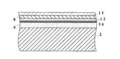
図1に、この発明の一実施例による強誘電体キャパシタの構造を示す。シリコン基板2の上に、酸化シリコン層4、下部電極12、強誘電体膜(強誘電体層)8、上部電極15が設けられている。下部電極12は酸化パラジウム(PdOx)によって形成されており、上部電極15も酸化パラジウム(PdOx)によって形成されている。
【0030】
従来例の図11に示すように、白金は柱状の結晶であるため、強誘電体膜8中の酸素を透過してしまう。この実施例では、酸化パラジウムを下部電極12として用いている。この酸化パラジウム層12は、柱状結晶でないため酸素を透過しにくい。したがって、強誘電体膜8の酸素の欠乏を防ぐことができる。上部電極15についても同様である。これにより、強誘電体膜8の強誘電性が向上した。つまり、上部電極15または下部電極12のいずれかを酸化パラジウムで構成すると、白金で構成した場合に比べて残留分極Prの使用による劣化がかなり改善されたなお、上記実施例では、下部電極12、上部電極15の双方を酸化パラジウムによって形成しているので、酸素やPbの透過を確実に防止することができる。しかし、何れか一方だけでも、ある程度の効果を得ることができる。
【0031】
上記のような強誘電体キャパシタは、たとえば、図2に示すように、トランジスタ24と組み合わせて、不揮発性メモリとして用いることができる。
【0032】
図3に、この発明の一実施例による強誘電体キャパシタの製造工程を示す。シリコン基板2の表面を熱酸化し、酸化シリコン層4を形成する(図3A)。ここでは、酸化シリコン層4の厚さを600nmとした。次に、パラジウムをターゲットとして用いて、反応性スパッタリングにより酸化パラジウムを、酸化シリコン層4の上に形成し、これを下部電極12とする(図3B)。ここでは、200nmの厚さに形成した。
【0033】
次に、この下部電極12の上に、ゾルゲル法によって、強誘電体層8としてPZT膜を形成する(図3C)。出発原料として、Pb(CH3COO)2 3H2O,Zr(tーOC4H9)4、Ti(i-OC3H7)4の混合溶液を用いた。この混合溶液をスピンコートした後、150度(摂氏、以下同じ)で乾燥させ、ドライエアー雰囲気において400度で30秒の仮焼成を行った。これを5回繰り返した後、O2雰囲気中で、700度以上の熱処理を施した。このようにして、250nmの強誘電体層8を形成した。なお、ここでは、PbZrxTi1-xO3において、xを0.52として(以下PZT(52・48)と表わす)、PZT膜を形成している。
【0034】
さらに、強誘電体層8の上に、反応性スパッタリングにより酸化パラジウムを形成し、上部電極15とする(図3D)。ここでは、200nmの厚さに形成した。このようにして、強誘電体キャパシタを得ることができる。
【0035】
なお、酸化パラジウムに代えて、WOx,TiOx,TaOx,IrO2,PtO2,ReOx,RuOx,OsOxを用いてもよい。
【0036】
また、これら酸化層の上に強誘電体を形成すると、強誘電体の配向性が損なわれる。そこで、酸化層の上にW層、Ti層、Ta層、Ir層、Pt層、Ru層、Re層、Pd層、Os層等の導電体層を設け、その上に強誘電体を形成してもよい。さらに、このような導電体層を設けることにより、強誘電体のリークを減少させることができた、図4に、この発明の他の実施例による強誘電体キャパシタの構造を示す。この実施例では、下部電極12と酸化シリコン層4との間に、チタン層(5nm)を接合層30として設けている。一般に、酸化パラジウムと酸化シリコンとの密着性はあまり良くない。このため、部分的に合金層がはがれ、強誘電特性を劣化させるおそれがある。そこで、この実施例では、酸化シリコン層4と密着性のよいチタン層を接合層30として設けている。これにより、強誘電特性を改善している。なお、チタン層は、スパッタリングによって形成すればよい。
【0037】
なお、上記実施例では、接合層30としてチタン層を用いたが、接合性を改善する材料であれば、どのようなものでもよい。例えば、白金層を用いてもよい。
【0038】
上記各実施例では、強誘電体膜8としてPZTを用いているが、酸化物強誘電体であれば、どのようなものを用いてもよい。たとえば、Ba4Ti3O12を用いてもよい。
【0039】
この発明の他の実施例によるキャパシタを図5に示す。この実施例では、強誘電体層8に代えて、高誘電率を有する誘電体層90を用いている。酸化シリコン層4の上に、酸化パラジウムの下部電極12を設け、その上にSrTiO3,(Sr,Ba)TiO3のペロブスカイト構造を有する高誘電率薄膜を誘電体層90として形成した。この場合も、強誘電体の場合と同様、誘電性の改善が図られた。つまり、強誘電体層について述べたことが、高誘電率を有する誘電体層にも適用できることが明らかとなった。
【0040】
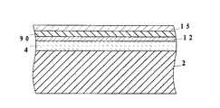
図5に、この発明の他の実施例による強誘電体キャパシタの構造を示す。シリコン基板2の上に、酸化シリコン層4、下部電極12、強誘電体膜(強誘電体層)8、上部電極15が設けられている。下部電極12は、パラジウム層11とその上に形成された酸化パラジウム層によって形成されている。また、上部電極15は、パラジウム層7とその上に形成された酸化パラジウム層9によって形成されている。
【0041】
下部電極12近傍の拡大図を、図7に示す。パラジウム層11は、柱状の結晶であるため、強誘電体膜8中の酸素を透過してしまう。この実施例では、パラジウム層11の上部表面に酸化パラジウム層13を形成している。前述のように、この酸化パラジウム層13によって強誘電体膜8の酸素の欠乏を防ぐことができる。上部電極15についても同様である。
【0042】
上記実施例では、下部電極12、上部電極15の双方に酸化パラジウム層を形成しているので、経年変化の少ない優れた特性の強誘電体キャパシタを得ることができる。なお、下部電極12、上部電極15の何れか一方を、上記の構造にしても、ある程度の効果は得られる。
【0043】
図8に、この強誘電体キャパシタの製造工程を示す。シリコン基板2の表面を熱酸化し、酸化シリコン層4を形成する(図8A)。ここでは、酸化シリコン層4の厚さを600nmとした。次に、パラジウムをターゲットとして用いて、パラジウム層11を、酸化シリコン層4の上に形成する(図8B)。次に、O2雰囲気中で800度、1分の熱処理を行い、パラジウム層11の表面に酸化パラジウム層13を形成する。このパラジウム層11と酸化パラジウム層13を、下部電極12とする。ここでは、下部電極を、200nmの厚さに形成した。
【0044】
次に、この下部電極12の上に、ゾルゲル法によって、強誘電体層8としてPZT膜を形成する(図8C)。出発原料として、Pb(CH3COO)2 3H2O,Zr(tーOC4H9)4、Ti(i-OC3H7)4の混合溶液を用いた。この混合溶液をスピンコートした後、150度(摂氏、以下同じ)で乾燥させ、ドライエアー雰囲気において400度で30秒の仮焼成を行った。これを5回繰り返した後、O2雰囲気中で、700度以上の熱処理を施した。このようにして、250nmの強誘電体層8を形成した。なお、ここでは、PbZrXTi1-XO3において、xを0.52として(以下PZT(52・48)と表わす)、PZT膜を形成している。
【0045】
さらに、強誘電体層8の上に、スパッタリングによりパラジウム層7を形成する。次に、O2雰囲気中で800度、1分の熱処理を行い、パラジウム層7の表面に酸化パラジウム層9を形成する(図8D)。このパラジウム層7と酸化パラジウム層9を、上部電極15とする。ここでは、上部電極15を、200nmの厚さに形成した。このようにして、強誘電体キャパシタを得ることができる。
【0046】
なお、この実施例についても、図4で説明したような接合層30を設けることが好ましい。
【0047】
また、ここで説明したパラジウムの表面を酸化するという実施例は、強誘電体膜だけでなく前述の高誘電率を有する誘電体膜にも適用でき、同様の効果を得ることができる。
【0048】
上記のように、パラジウム層の表面を酸化することにより強誘電体膜の酸素の抜け出しを防止できるが、表面に酸化パラジウムが形成されて、強誘電体膜の配向性が悪くなる。これは、既に述べたように、酸化パラジウム層13の上に、W層、Ti層、Ta層、Ir層、Pt層、Ru層、Re層、Pd層、Os層等の導電体層を設けることにより解決できる。しかし、次のようにして、下部電極を形成しても解決できる。
【0049】
まず、図9に示すように、パラジウム層11の上に白金層80(薄膜導電体)をごく薄く設ける。ここでは、30nmとした。次に、この状態で熱処理を行う。表面の白金層80は酸素と反応しないので、酸化されない。また、白金層80は、薄く形成されているので、その下のパラジウム層11の結晶間が酸化され、酸化パラジウムが形成されて酸素の透過を防ぐ。したがって、表面は配向性に優れたままでありながら、酸素の透過を防ぐことのできる下部電極12を形成することができる。
【0050】
なお、このような薄膜白金層80を形成したのち酸化したパラジウム層11は、単独で下部電極12として使用できる。しかし、スパッタリングで形成した酸化パラジウム層の上に配向性の良い導電層(パラジウム層、白金層等)を設けて配向性を改善した実施例においての、配向性の良い導電層として用いることもできる。
【0051】
また、ここで説明した実施例は、強誘電体膜だけでなく前述の高誘電率を有する誘電体膜にも適用でき、同様の効果を得ることができる。
【図面の簡単な説明】
【図1】この発明の一実施例による強誘電体キャパシタの構図を示す図である。
【図2】強誘電体キャパシタ22を用いた不揮発性メモリを示す図である。
【図3】強誘電体キャパシタの製造工程を示す図である。
【図4】接合層30を設けた実施例を示す図である。
【図5】高誘電率を有する誘電体90を用いた場合の実施例を示す図である。
【図6】他の実施例による強誘電体キャパシタの構造を示す図である。
【図7】酸化パラジウム層が酸素の抜け出しを防止するメカニズムを示す図である。
【図8】図22の強誘電体キャパシタの製造工程を示す図である。
【図9】パラジウムの表面に薄膜白金を設けて酸化を行う実施例を示す図である。
【図10】従来の強誘電体キャパシタの構造を示す図である。
【図11】白金による下部電極6から酸素が抜け出す状態を示す図である。
【符号の説明】
2...シリコン基板
4...酸化シリコン層
8...強誘電体層
12...下部電極
15...上部電極
90...高誘電率を有する誘電体層
Claims (2)
- 下部電極と、前記下部電極の上に形成され、強誘電体または高誘電率を有する誘電体によって構成される誘電体層と、前記誘電体層の上に形成された上部電極と、を備え、前記下部電極はパラジウムの柱状結晶間にその酸化物である酸化パラジウムを有する単独の層であることを特徴とする、誘電体キャパシタ。
- 下部電極を形成するステップと、前記下部電極の上に強誘電体または高誘電率を有する誘電体によって構成される誘電体層を形成するステップと、前記誘電体層の上に上部電極を形成するステップとを備える誘電体キャパシタの製造方法であって、前記下部電極を形成するステップは、柱状結晶構造を有するパラジウムの薄膜を形成する工程と、前記パラジウムの薄膜上に白金の薄膜を形成する工程と、前記パラジウムは酸化する一方前記白金は酸化しない条件の酸化雰囲気中で熱処理を行い、前記パラジウムの薄膜の柱状結晶間のみに酸化パラジウムを形成する工程と、前記白金の薄膜のみを選択的に除去する工程とからなる、ことを特徴とする、誘電体キャパシタの製造方法。
Priority Applications (13)
| Application Number | Priority Date | Filing Date | Title |
|---|---|---|---|
| JP17214295A JP3929513B2 (ja) | 1995-07-07 | 1995-07-07 | 誘電体キャパシタおよびその製造方法 |
| KR1019960706383A KR100385446B1 (ko) | 1995-07-07 | 1996-07-05 | 유전체캐패시터및그제조방법 |
| DE69633554T DE69633554T2 (de) | 1995-07-07 | 1996-07-05 | Festdielektrikumkondensator und verfahren zu seiner herstellung |
| CN96190228A CN1085411C (zh) | 1995-07-07 | 1996-07-05 | 电介质电容器及其制造方法 |
| EP96922252A EP0785579B1 (en) | 1995-07-07 | 1996-07-05 | Dielectric capacitor and process for preparing the same |
| EP04076904A EP1467400A3 (en) | 1995-07-07 | 1996-07-05 | Capacitor |
| PCT/JP1996/001883 WO1997003468A1 (fr) | 1995-07-07 | 1996-07-05 | Condensateurs dielectriques et leur procede de fabrication |
| CA002197491A CA2197491C (en) | 1995-07-07 | 1996-07-05 | Ferroelectric capacitor and method for manufacturing thereof |
| US08/812,059 US6454914B1 (en) | 1995-07-07 | 1997-02-20 | Ferroelectric capacitor and a method for manufacturing thereof |
| US10/215,844 US6693791B2 (en) | 1995-07-07 | 2002-08-08 | Ferroelectric capacitor and a method for manufacturing thereof |
| US10/651,435 US6873517B2 (en) | 1995-07-07 | 2003-08-29 | Ferroelectric capacitor |
| US11/015,082 US7057874B2 (en) | 1995-07-07 | 2004-12-16 | Ferroelectric capacitor |
| US11/279,495 US7443649B2 (en) | 1995-07-07 | 2006-04-12 | Ferroelectric capacitor |
Applications Claiming Priority (1)
| Application Number | Priority Date | Filing Date | Title |
|---|---|---|---|
| JP17214295A JP3929513B2 (ja) | 1995-07-07 | 1995-07-07 | 誘電体キャパシタおよびその製造方法 |
Related Child Applications (2)
| Application Number | Title | Priority Date | Filing Date |
|---|---|---|---|
| JP2007011924A Division JP4255495B2 (ja) | 2007-01-22 | 2007-01-22 | 誘電体キャパシタ |
| JP2007011923A Division JP2007184623A (ja) | 2007-01-22 | 2007-01-22 | 誘電体キャパシタ |
Publications (2)
| Publication Number | Publication Date |
|---|---|
| JPH0922829A JPH0922829A (ja) | 1997-01-21 |
| JP3929513B2 true JP3929513B2 (ja) | 2007-06-13 |
Family
ID=15936351
Family Applications (1)
| Application Number | Title | Priority Date | Filing Date |
|---|---|---|---|
| JP17214295A Expired - Fee Related JP3929513B2 (ja) | 1995-07-07 | 1995-07-07 | 誘電体キャパシタおよびその製造方法 |
Country Status (8)
| Country | Link |
|---|---|
| US (5) | US6454914B1 (ja) |
| EP (2) | EP1467400A3 (ja) |
| JP (1) | JP3929513B2 (ja) |
| KR (1) | KR100385446B1 (ja) |
| CN (1) | CN1085411C (ja) |
| CA (1) | CA2197491C (ja) |
| DE (1) | DE69633554T2 (ja) |
| WO (1) | WO1997003468A1 (ja) |
Families Citing this family (36)
| Publication number | Priority date | Publication date | Assignee | Title |
|---|---|---|---|---|
| JP3929513B2 (ja) * | 1995-07-07 | 2007-06-13 | ローム株式会社 | 誘電体キャパシタおよびその製造方法 |
| US6699304B1 (en) * | 1997-02-24 | 2004-03-02 | Superior Micropowders, Llc | Palladium-containing particles, method and apparatus of manufacture, palladium-containing devices made therefrom |
| KR100434479B1 (ko) * | 1997-07-10 | 2004-09-18 | 삼성전자주식회사 | 고집적 페로일렉트릭 플로팅게이트 램 및 그 제조방법 |
| JP3517876B2 (ja) | 1998-10-14 | 2004-04-12 | セイコーエプソン株式会社 | 強誘電体薄膜素子の製造方法、インクジェット式記録ヘッド及びインクジェットプリンタ |
| DE19929307C1 (de) | 1999-06-25 | 2000-11-09 | Siemens Ag | Verfahren zur Herstellung einer strukturierten Schicht und dadurch hergestellte Elektrode |
| KR100600261B1 (ko) * | 1999-12-29 | 2006-07-13 | 주식회사 하이닉스반도체 | 반도체 소자의 캐패시터 형성방법 |
| US6214661B1 (en) * | 2000-01-21 | 2001-04-10 | Infineon Technologoies North America Corp. | Method to prevent oxygen out-diffusion from BSTO containing micro-electronic device |
| JP4228560B2 (ja) * | 2000-11-01 | 2009-02-25 | ソニー株式会社 | キャパシタ素子及びその製造方法 |
| US7378719B2 (en) * | 2000-12-20 | 2008-05-27 | Micron Technology, Inc. | Low leakage MIM capacitor |
| JP4428500B2 (ja) | 2001-07-13 | 2010-03-10 | 富士通マイクロエレクトロニクス株式会社 | 容量素子及びその製造方法 |
| US7335552B2 (en) * | 2002-05-15 | 2008-02-26 | Raytheon Company | Electrode for thin film capacitor devices |
| JP2003332539A (ja) * | 2002-05-17 | 2003-11-21 | Nec Electronics Corp | 強誘電体キャパシタ及びその製造方法並びに半導体記憶装置 |
| KR100487528B1 (ko) * | 2002-06-26 | 2005-05-03 | 삼성전자주식회사 | 피로 현상을 억제하기 위한 금속산화막을 갖는 강유전체캐패시터 및 그 제조방법 |
| JP2004296929A (ja) * | 2003-03-27 | 2004-10-21 | Seiko Epson Corp | 強誘電体キャパシタの製造方法、強誘電体キャパシタ、記憶素子、電子素子、メモリ装置及び電子機器 |
| US7030463B1 (en) * | 2003-10-01 | 2006-04-18 | University Of Dayton | Tuneable electromagnetic bandgap structures based on high resistivity silicon substrates |
| US20070069264A1 (en) * | 2003-10-20 | 2007-03-29 | Guru Subramanyam | Ferroelectric varactors suitable for capacitive shunt switching and wireless sensing |
| US7692270B2 (en) * | 2003-10-20 | 2010-04-06 | University Of Dayton | Ferroelectric varactors suitable for capacitive shunt switching |
| US7719392B2 (en) * | 2003-10-20 | 2010-05-18 | University Of Dayton | Ferroelectric varactors suitable for capacitive shunt switching |
| US7268643B2 (en) * | 2004-01-28 | 2007-09-11 | Paratek Microwave, Inc. | Apparatus, system and method capable of radio frequency switching using tunable dielectric capacitors |
| JP4220459B2 (ja) * | 2004-11-22 | 2009-02-04 | 株式会社東芝 | 半導体装置 |
| WO2006131968A1 (ja) | 2005-06-09 | 2006-12-14 | Fujitsu Limited | 半導体装置及びその製造方法 |
| US7345331B1 (en) | 2005-09-23 | 2008-03-18 | United States Of America As Represented By The Secretary Of The Navy | Ferroelectric capacitor circuit for sensing hydrogen gas |
| US8460519B2 (en) * | 2005-10-28 | 2013-06-11 | Applied Materials Inc. | Protective offset sputtering |
| US8454804B2 (en) * | 2005-10-28 | 2013-06-04 | Applied Materials Inc. | Protective offset sputtering |
| US7389675B1 (en) | 2006-05-12 | 2008-06-24 | The United States Of America As Represented By The National Aeronautics And Space Administration | Miniaturized metal (metal alloy)/ PdOx/SiC hydrogen and hydrocarbon gas sensors |
| US8247855B2 (en) * | 2006-09-12 | 2012-08-21 | Texas Instruments Incorporated | Enhanced local interconnects employing ferroelectric electrodes |
| JP2007184623A (ja) * | 2007-01-22 | 2007-07-19 | Rohm Co Ltd | 誘電体キャパシタ |
| US8058636B2 (en) * | 2007-03-29 | 2011-11-15 | Panasonic Corporation | Variable resistance nonvolatile memory apparatus |
| US7971171B2 (en) * | 2007-07-03 | 2011-06-28 | International Business Machines Corporation | Method and system for electromigration analysis on signal wiring |
| US7922975B2 (en) * | 2008-07-14 | 2011-04-12 | University Of Dayton | Resonant sensor capable of wireless interrogation |
| JP5347381B2 (ja) * | 2008-08-28 | 2013-11-20 | 富士通セミコンダクター株式会社 | 半導体装置の製造方法 |
| US20100096678A1 (en) * | 2008-10-20 | 2010-04-22 | University Of Dayton | Nanostructured barium strontium titanate (bst) thin-film varactors on sapphire |
| CN102157262B (zh) * | 2011-03-10 | 2012-09-05 | 苏州大学 | 一种以Ta2O5薄膜为电介质膜的电容器制备方法 |
| US9000866B2 (en) | 2012-06-26 | 2015-04-07 | University Of Dayton | Varactor shunt switches with parallel capacitor architecture |
| RU2550090C2 (ru) * | 2013-03-06 | 2015-05-10 | Открытое Акционерное общество "Научно-исследовательский институт "Гириконд" | Тонкопленочный вариконд |
| CN113278935B (zh) * | 2021-05-07 | 2022-12-09 | 昆明贵研新材料科技有限公司 | 一种氧化铂电极及其制备方法和用途 |
Family Cites Families (28)
| Publication number | Priority date | Publication date | Assignee | Title |
|---|---|---|---|---|
| US3616400A (en) * | 1968-03-25 | 1971-10-26 | Matsushita Electric Ind Co Ltd | Method of making thin film capacitor |
| US5214300A (en) * | 1970-09-28 | 1993-05-25 | Ramtron Corporation | Monolithic semiconductor integrated circuit ferroelectric memory device |
| JPS4870855A (ja) * | 1971-12-29 | 1973-09-26 | ||
| US3969197A (en) * | 1974-02-08 | 1976-07-13 | Texas Instruments Incorporated | Method for fabricating a thin film capacitor |
| DE2513858C3 (de) * | 1975-03-27 | 1981-08-06 | Siemens AG, 1000 Berlin und 8000 München | Verfahren zur Herstellung eines Tantal-Dünnschichtkondensators |
| US4038167A (en) * | 1976-02-09 | 1977-07-26 | Corning Glass Works | Method of forming a thin film capacitor |
| US5005102A (en) * | 1989-06-20 | 1991-04-02 | Ramtron Corporation | Multilayer electrodes for integrated circuit capacitors |
| US4982309A (en) | 1989-07-17 | 1991-01-01 | National Semiconductor Corporation | Electrodes for electrical ceramic oxide devices |
| US5122923A (en) * | 1989-08-30 | 1992-06-16 | Nec Corporation | Thin-film capacitors and process for manufacturing the same |
| JPH0712074B2 (ja) | 1990-03-01 | 1995-02-08 | 日本電気株式会社 | 薄膜コンデンサ及びその製造方法 |
| DE69125323T2 (de) * | 1990-07-24 | 1997-09-25 | Semiconductor Energy Lab | Verfahren zum Herstellen isolierender Filme, Kapazitäten und Halbleiteranordnungen |
| DE69205063T2 (de) * | 1991-05-16 | 1996-02-29 | Nippon Electric Co | Dünnschichtkondensator. |
| US5142437A (en) | 1991-06-13 | 1992-08-25 | Ramtron Corporation | Conducting electrode layers for ferroelectric capacitors in integrated circuits and method |
| US5164808A (en) * | 1991-08-09 | 1992-11-17 | Radiant Technologies | Platinum electrode structure for use in conjunction with ferroelectric materials |
| US5723361A (en) * | 1991-12-13 | 1998-03-03 | Symetrix Corporation | Thin films of ABO3 with excess A-site and B-site modifiers and method of fabricating integrated circuits with same |
| US5191510A (en) * | 1992-04-29 | 1993-03-02 | Ramtron International Corporation | Use of palladium as an adhesion layer and as an electrode in ferroelectric memory devices |
| JP3407204B2 (ja) * | 1992-07-23 | 2003-05-19 | オリンパス光学工業株式会社 | 強誘電体集積回路及びその製造方法 |
| US5348894A (en) * | 1993-01-27 | 1994-09-20 | Texas Instruments Incorporated | Method of forming electrical connections to high dielectric constant materials |
| JP2629586B2 (ja) * | 1993-12-16 | 1997-07-09 | 日本電気株式会社 | 半導体デバイスおよびその製造方法 |
| JP3461398B2 (ja) | 1994-01-13 | 2003-10-27 | ローム株式会社 | 誘電体キャパシタおよびその製造方法 |
| US6052271A (en) * | 1994-01-13 | 2000-04-18 | Rohm Co., Ltd. | Ferroelectric capacitor including an iridium oxide layer in the lower electrode |
| JPH088403A (ja) * | 1994-06-17 | 1996-01-12 | Sharp Corp | 強誘電体結晶薄膜被覆基板及び該基板を含む強誘電体薄膜素子及び該強誘電体薄膜素子の製造方法 |
| DE4421007A1 (de) | 1994-06-18 | 1995-12-21 | Philips Patentverwaltung | Elektronisches Bauteil und Verfahren zu seiner Herstellung |
| JP2755174B2 (ja) * | 1994-06-21 | 1998-05-20 | 日本電気株式会社 | 強誘電体容量及びメモリセル構造 |
| JP3188361B2 (ja) * | 1994-06-27 | 2001-07-16 | ペルメレック電極株式会社 | クロムめっき方法 |
| JPH08162619A (ja) * | 1994-12-09 | 1996-06-21 | Hitachi Ltd | 半導体装置及びその製造方法 |
| US5753945A (en) * | 1995-06-29 | 1998-05-19 | Northern Telecom Limited | Integrated circuit structure comprising a zirconium titanium oxide barrier layer and method of forming a zirconium titanium oxide barrier layer |
| JP3929513B2 (ja) * | 1995-07-07 | 2007-06-13 | ローム株式会社 | 誘電体キャパシタおよびその製造方法 |
-
1995
- 1995-07-07 JP JP17214295A patent/JP3929513B2/ja not_active Expired - Fee Related
-
1996
- 1996-07-05 KR KR1019960706383A patent/KR100385446B1/ko not_active IP Right Cessation
- 1996-07-05 CA CA002197491A patent/CA2197491C/en not_active Expired - Fee Related
- 1996-07-05 WO PCT/JP1996/001883 patent/WO1997003468A1/ja active IP Right Grant
- 1996-07-05 EP EP04076904A patent/EP1467400A3/en not_active Withdrawn
- 1996-07-05 CN CN96190228A patent/CN1085411C/zh not_active Expired - Fee Related
- 1996-07-05 DE DE69633554T patent/DE69633554T2/de not_active Expired - Fee Related
- 1996-07-05 EP EP96922252A patent/EP0785579B1/en not_active Expired - Lifetime
-
1997
- 1997-02-20 US US08/812,059 patent/US6454914B1/en not_active Expired - Lifetime
-
2002
- 2002-08-08 US US10/215,844 patent/US6693791B2/en not_active Expired - Lifetime
-
2003
- 2003-08-29 US US10/651,435 patent/US6873517B2/en not_active Expired - Fee Related
-
2004
- 2004-12-16 US US11/015,082 patent/US7057874B2/en not_active Expired - Fee Related
-
2006
- 2006-04-12 US US11/279,495 patent/US7443649B2/en not_active Expired - Fee Related
Also Published As
| Publication number | Publication date |
|---|---|
| EP0785579A1 (en) | 1997-07-23 |
| US6873517B2 (en) | 2005-03-29 |
| US20060170021A1 (en) | 2006-08-03 |
| US20040036105A1 (en) | 2004-02-26 |
| US6454914B1 (en) | 2002-09-24 |
| CN1155943A (zh) | 1997-07-30 |
| US6693791B2 (en) | 2004-02-17 |
| KR100385446B1 (ko) | 2004-09-08 |
| EP1467400A3 (en) | 2004-10-20 |
| US7443649B2 (en) | 2008-10-28 |
| DE69633554D1 (de) | 2004-11-11 |
| CA2197491A1 (en) | 1997-01-30 |
| EP0785579B1 (en) | 2004-10-06 |
| DE69633554T2 (de) | 2005-10-13 |
| CA2197491C (en) | 2002-01-01 |
| JPH0922829A (ja) | 1997-01-21 |
| US20020189933A1 (en) | 2002-12-19 |
| CN1085411C (zh) | 2002-05-22 |
| US7057874B2 (en) | 2006-06-06 |
| US20050098819A1 (en) | 2005-05-12 |
| WO1997003468A1 (fr) | 1997-01-30 |
| EP1467400A2 (en) | 2004-10-13 |
| EP0785579A4 (en) | 1998-10-14 |
| KR970703049A (ko) | 1997-06-10 |
Similar Documents
| Publication | Publication Date | Title |
|---|---|---|
| JP3929513B2 (ja) | 誘電体キャパシタおよびその製造方法 | |
| JP3319994B2 (ja) | 半導体記憶素子 | |
| JP4024397B2 (ja) | 強誘電体メモリ装置及びその製造方法 | |
| JP3452763B2 (ja) | 半導体記憶装置および半導体記憶装置の製造方法 | |
| JPH09260600A (ja) | 半導体メモリ素子の製造方法 | |
| JP2003068988A (ja) | 強誘電膜を平坦化膜として用いる強誘電体メモリ装置およびその製造方法。 | |
| JP3419665B2 (ja) | 半導体装置の製造方法 | |
| JP3461398B2 (ja) | 誘電体キャパシタおよびその製造方法 | |
| JP3349612B2 (ja) | 誘電体キャパシタおよびその製造方法 | |
| JP3981142B2 (ja) | 強誘電体キャパシタおよびその製造方法 | |
| JPH11307736A (ja) | 半導体メモリ素子の製造方法 | |
| JP3954390B2 (ja) | 誘電体キャパシタ | |
| JP3294214B2 (ja) | 薄膜キャパシタ | |
| JP3363091B2 (ja) | 誘電体メモリの製造方法 | |
| JP3419974B2 (ja) | 強誘電体キャパシタの製造方法 | |
| JP4255495B2 (ja) | 誘電体キャパシタ | |
| JP4074894B2 (ja) | 強誘電体メモリ及びその製造方法 | |
| JPH0620866A (ja) | 誘電体素子 | |
| KR100288688B1 (ko) | 반도체메모리소자의제조방법 | |
| JP2007184623A (ja) | 誘電体キャパシタ | |
| JP2003243628A (ja) | 強誘電体薄膜、強誘電体キャパシタ、及び強誘電体メモリ素子の製造方法 | |
| JPH0897382A (ja) | 半導体メモリ素子 | |
| JP2000031399A (ja) | 誘電体素子及び半導体記憶装置 | |
| JPH05343697A (ja) | 誘電体素子 | |
| JPH10229169A (ja) | 強誘電体記憶素子及びその製造方法、並びに集積回路 |
Legal Events
| Date | Code | Title | Description |
|---|---|---|---|
| A131 | Notification of reasons for refusal |
Free format text: JAPANESE INTERMEDIATE CODE: A131 Effective date: 20040324 |
|
| A521 | Request for written amendment filed |
Free format text: JAPANESE INTERMEDIATE CODE: A523 Effective date: 20040521 |
|
| A02 | Decision of refusal |
Free format text: JAPANESE INTERMEDIATE CODE: A02 Effective date: 20041124 |
|
| A521 | Request for written amendment filed |
Free format text: JAPANESE INTERMEDIATE CODE: A523 Effective date: 20050121 |
|
| RD04 | Notification of resignation of power of attorney |
Free format text: JAPANESE INTERMEDIATE CODE: A7424 Effective date: 20060425 |
|
| A521 | Request for written amendment filed |
Free format text: JAPANESE INTERMEDIATE CODE: A523 Effective date: 20070122 |
|
| A61 | First payment of annual fees (during grant procedure) |
Free format text: JAPANESE INTERMEDIATE CODE: A61 Effective date: 20070307 |
|
| R150 | Certificate of patent or registration of utility model |
Free format text: JAPANESE INTERMEDIATE CODE: R150 |
|
| A521 | Request for written amendment filed |
Free format text: JAPANESE INTERMEDIATE CODE: A523 Effective date: 20070122 |
|
| LAPS | Cancellation because of no payment of annual fees |