EP1467400A2 - Capacitor - Google Patents
Capacitor Download PDFInfo
- Publication number
- EP1467400A2 EP1467400A2 EP04076904A EP04076904A EP1467400A2 EP 1467400 A2 EP1467400 A2 EP 1467400A2 EP 04076904 A EP04076904 A EP 04076904A EP 04076904 A EP04076904 A EP 04076904A EP 1467400 A2 EP1467400 A2 EP 1467400A2
- Authority
- EP
- European Patent Office
- Prior art keywords
- layer
- layer made
- lower electrode
- ferroelectric
- capacitor
- Prior art date
- Legal status (The legal status is an assumption and is not a legal conclusion. Google has not performed a legal analysis and makes no representation as to the accuracy of the status listed.)
- Withdrawn
Links
- 239000003990 capacitor Substances 0.000 title claims abstract description 65
- 238000007254 oxidation reaction Methods 0.000 claims abstract description 61
- 230000003647 oxidation Effects 0.000 claims abstract description 57
- XUIMIQQOPSSXEZ-UHFFFAOYSA-N Silicon Chemical compound [Si] XUIMIQQOPSSXEZ-UHFFFAOYSA-N 0.000 claims abstract description 36
- 229910052710 silicon Inorganic materials 0.000 claims abstract description 36
- 239000010703 silicon Substances 0.000 claims abstract description 36
- 239000000126 substance Substances 0.000 claims abstract description 27
- 239000000758 substrate Substances 0.000 claims abstract description 25
- 229910052697 platinum Inorganic materials 0.000 claims abstract description 23
- 229910052763 palladium Inorganic materials 0.000 claims abstract description 21
- 229910019020 PtO2 Inorganic materials 0.000 claims abstract description 20
- 229910019897 RuOx Inorganic materials 0.000 claims abstract description 20
- 229910003070 TaOx Inorganic materials 0.000 claims abstract description 20
- 229910003087 TiOx Inorganic materials 0.000 claims abstract description 20
- YKIOKAURTKXMSB-UHFFFAOYSA-N adams's catalyst Chemical compound O=[Pt]=O YKIOKAURTKXMSB-UHFFFAOYSA-N 0.000 claims abstract description 20
- HTXDPTMKBJXEOW-UHFFFAOYSA-N iridium(IV) oxide Inorganic materials O=[Ir]=O HTXDPTMKBJXEOW-UHFFFAOYSA-N 0.000 claims abstract description 20
- HLLICFJUWSZHRJ-UHFFFAOYSA-N tioxidazole Chemical compound CCCOC1=CC=C2N=C(NC(=O)OC)SC2=C1 HLLICFJUWSZHRJ-UHFFFAOYSA-N 0.000 claims abstract description 20
- 239000013078 crystal Substances 0.000 claims abstract description 11
- 239000000463 material Substances 0.000 claims abstract description 11
- 229910052719 titanium Inorganic materials 0.000 claims abstract description 7
- -1 ReOx Inorganic materials 0.000 claims abstract description 5
- 229910002673 PdOx Inorganic materials 0.000 claims abstract 4
- 229910052741 iridium Inorganic materials 0.000 claims abstract 3
- 229910052762 osmium Inorganic materials 0.000 claims abstract 3
- 229910052702 rhenium Inorganic materials 0.000 claims abstract 3
- 229910052715 tantalum Inorganic materials 0.000 claims abstract 3
- 229910052721 tungsten Inorganic materials 0.000 claims abstract 3
- 229910052707 ruthenium Inorganic materials 0.000 claims abstract 2
- BASFCYQUMIYNBI-UHFFFAOYSA-N platinum Chemical compound [Pt] BASFCYQUMIYNBI-UHFFFAOYSA-N 0.000 description 56
- KDLHZDBZIXYQEI-UHFFFAOYSA-N palladium Substances [Pd] KDLHZDBZIXYQEI-UHFFFAOYSA-N 0.000 description 50
- HBEQXAKJSGXAIQ-UHFFFAOYSA-N oxopalladium Chemical compound [Pd]=O HBEQXAKJSGXAIQ-UHFFFAOYSA-N 0.000 description 47
- 229910003445 palladium oxide Inorganic materials 0.000 description 45
- 239000010408 film Substances 0.000 description 40
- 238000000034 method Methods 0.000 description 28
- 239000010936 titanium Substances 0.000 description 26
- 229910052760 oxygen Inorganic materials 0.000 description 21
- QVGXLLKOCUKJST-UHFFFAOYSA-N atomic oxygen Chemical compound [O] QVGXLLKOCUKJST-UHFFFAOYSA-N 0.000 description 19
- 239000001301 oxygen Substances 0.000 description 19
- 238000004519 manufacturing process Methods 0.000 description 15
- 230000005621 ferroelectricity Effects 0.000 description 14
- 230000015556 catabolic process Effects 0.000 description 8
- 238000006731 degradation reaction Methods 0.000 description 8
- 230000001590 oxidative effect Effects 0.000 description 7
- VYPSYNLAJGMNEJ-UHFFFAOYSA-N Silicium dioxide Chemical compound O=[Si]=O VYPSYNLAJGMNEJ-UHFFFAOYSA-N 0.000 description 6
- 230000032683 aging Effects 0.000 description 6
- 229910052814 silicon oxide Inorganic materials 0.000 description 6
- 230000008901 benefit Effects 0.000 description 5
- 238000007669 thermal treatment Methods 0.000 description 5
- RTAQQCXQSZGOHL-UHFFFAOYSA-N Titanium Chemical compound [Ti] RTAQQCXQSZGOHL-UHFFFAOYSA-N 0.000 description 4
- 239000011259 mixed solution Substances 0.000 description 4
- 230000015572 biosynthetic process Effects 0.000 description 3
- 230000003247 decreasing effect Effects 0.000 description 3
- 230000010287 polarization Effects 0.000 description 3
- 230000008569 process Effects 0.000 description 3
- 229910020684 PbZr Inorganic materials 0.000 description 2
- 230000006872 improvement Effects 0.000 description 2
- 230000002265 prevention Effects 0.000 description 2
- 238000003980 solgel method Methods 0.000 description 2
- 238000004528 spin coating Methods 0.000 description 2
- 239000007858 starting material Substances 0.000 description 2
- 239000010409 thin film Substances 0.000 description 2
- 229910001252 Pd alloy Inorganic materials 0.000 description 1
- 229910002370 SrTiO3 Inorganic materials 0.000 description 1
- 229910010252 TiO3 Inorganic materials 0.000 description 1
- 230000032798 delamination Effects 0.000 description 1
- 208000002925 dental caries Diseases 0.000 description 1
- 238000010586 diagram Methods 0.000 description 1
- 238000009413 insulation Methods 0.000 description 1
- 239000012212 insulator Substances 0.000 description 1
- 230000007246 mechanism Effects 0.000 description 1
- 230000008520 organization Effects 0.000 description 1
Images


Classifications
-
- H—ELECTRICITY
- H01—ELECTRIC ELEMENTS
- H01L—SEMICONDUCTOR DEVICES NOT COVERED BY CLASS H10
- H01L29/00—Semiconductor devices adapted for rectifying, amplifying, oscillating or switching, or capacitors or resistors with at least one potential-jump barrier or surface barrier, e.g. PN junction depletion layer or carrier concentration layer; Details of semiconductor bodies or of electrodes thereof ; Multistep manufacturing processes therefor
- H01L29/66—Types of semiconductor device ; Multistep manufacturing processes therefor
- H01L29/86—Types of semiconductor device ; Multistep manufacturing processes therefor controllable only by variation of the electric current supplied, or only the electric potential applied, to one or more of the electrodes carrying the current to be rectified, amplified, oscillated or switched
- H01L29/92—Capacitors with potential-jump barrier or surface barrier
-
- H—ELECTRICITY
- H01—ELECTRIC ELEMENTS
- H01L—SEMICONDUCTOR DEVICES NOT COVERED BY CLASS H10
- H01L21/00—Processes or apparatus adapted for the manufacture or treatment of semiconductor or solid state devices or of parts thereof
- H01L21/02—Manufacture or treatment of semiconductor devices or of parts thereof
- H01L21/04—Manufacture or treatment of semiconductor devices or of parts thereof the devices having at least one potential-jump barrier or surface barrier, e.g. PN junction, depletion layer or carrier concentration layer
- H01L21/18—Manufacture or treatment of semiconductor devices or of parts thereof the devices having at least one potential-jump barrier or surface barrier, e.g. PN junction, depletion layer or carrier concentration layer the devices having semiconductor bodies comprising elements of Group IV of the Periodic System or AIIIBV compounds with or without impurities, e.g. doping materials
- H01L21/30—Treatment of semiconductor bodies using processes or apparatus not provided for in groups H01L21/20 - H01L21/26
- H01L21/31—Treatment of semiconductor bodies using processes or apparatus not provided for in groups H01L21/20 - H01L21/26 to form insulating layers thereon, e.g. for masking or by using photolithographic techniques; After treatment of these layers; Selection of materials for these layers
- H01L21/3205—Deposition of non-insulating-, e.g. conductive- or resistive-, layers on insulating layers; After-treatment of these layers
- H01L21/32051—Deposition of metallic or metal-silicide layers
-
- H—ELECTRICITY
- H01—ELECTRIC ELEMENTS
- H01L—SEMICONDUCTOR DEVICES NOT COVERED BY CLASS H10
- H01L27/00—Devices consisting of a plurality of semiconductor or other solid-state components formed in or on a common substrate
- H01L27/02—Devices consisting of a plurality of semiconductor or other solid-state components formed in or on a common substrate including semiconductor components specially adapted for rectifying, oscillating, amplifying or switching and having at least one potential-jump barrier or surface barrier; including integrated passive circuit elements with at least one potential-jump barrier or surface barrier
- H01L27/04—Devices consisting of a plurality of semiconductor or other solid-state components formed in or on a common substrate including semiconductor components specially adapted for rectifying, oscillating, amplifying or switching and having at least one potential-jump barrier or surface barrier; including integrated passive circuit elements with at least one potential-jump barrier or surface barrier the substrate being a semiconductor body
- H01L27/08—Devices consisting of a plurality of semiconductor or other solid-state components formed in or on a common substrate including semiconductor components specially adapted for rectifying, oscillating, amplifying or switching and having at least one potential-jump barrier or surface barrier; including integrated passive circuit elements with at least one potential-jump barrier or surface barrier the substrate being a semiconductor body including only semiconductor components of a single kind
- H01L27/0805—Capacitors only
-
- H—ELECTRICITY
- H01—ELECTRIC ELEMENTS
- H01L—SEMICONDUCTOR DEVICES NOT COVERED BY CLASS H10
- H01L28/00—Passive two-terminal components without a potential-jump or surface barrier for integrated circuits; Details thereof; Multistep manufacturing processes therefor
- H01L28/40—Capacitors
- H01L28/55—Capacitors with a dielectric comprising a perovskite structure material
- H01L28/56—Capacitors with a dielectric comprising a perovskite structure material the dielectric comprising two or more layers, e.g. comprising buffer layers, seed layers, gradient layers
-
- H—ELECTRICITY
- H01—ELECTRIC ELEMENTS
- H01L—SEMICONDUCTOR DEVICES NOT COVERED BY CLASS H10
- H01L28/00—Passive two-terminal components without a potential-jump or surface barrier for integrated circuits; Details thereof; Multistep manufacturing processes therefor
- H01L28/40—Capacitors
- H01L28/60—Electrodes
- H01L28/65—Electrodes comprising a noble metal or a noble metal oxide, e.g. platinum (Pt), ruthenium (Ru), ruthenium dioxide (RuO2), iridium (Ir), iridium dioxide (IrO2)
-
- H—ELECTRICITY
- H01—ELECTRIC ELEMENTS
- H01L—SEMICONDUCTOR DEVICES NOT COVERED BY CLASS H10
- H01L28/00—Passive two-terminal components without a potential-jump or surface barrier for integrated circuits; Details thereof; Multistep manufacturing processes therefor
- H01L28/40—Capacitors
- H01L28/60—Electrodes
- H01L28/75—Electrodes comprising two or more layers, e.g. comprising a barrier layer and a metal layer
-
- H—ELECTRICITY
- H01—ELECTRIC ELEMENTS
- H01L—SEMICONDUCTOR DEVICES NOT COVERED BY CLASS H10
- H01L21/00—Processes or apparatus adapted for the manufacture or treatment of semiconductor or solid state devices or of parts thereof
- H01L21/70—Manufacture or treatment of devices consisting of a plurality of solid state components formed in or on a common substrate or of parts thereof; Manufacture of integrated circuit devices or of parts thereof
- H01L21/71—Manufacture of specific parts of devices defined in group H01L21/70
- H01L21/768—Applying interconnections to be used for carrying current between separate components within a device comprising conductors and dielectrics
- H01L21/76838—Applying interconnections to be used for carrying current between separate components within a device comprising conductors and dielectrics characterised by the formation and the after-treatment of the conductors
- H01L21/76841—Barrier, adhesion or liner layers
-
- H—ELECTRICITY
- H01—ELECTRIC ELEMENTS
- H01L—SEMICONDUCTOR DEVICES NOT COVERED BY CLASS H10
- H01L28/00—Passive two-terminal components without a potential-jump or surface barrier for integrated circuits; Details thereof; Multistep manufacturing processes therefor
- H01L28/40—Capacitors
- H01L28/55—Capacitors with a dielectric comprising a perovskite structure material
Definitions
- the present invention relates to a ferroelectric capacitor, more specifically, improvement of ferroelectricity and other characteristics of the capacitor.
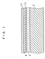
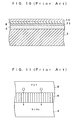
- Fig. 10 shows a conventional ferroelectric capacitor.
- a silicon oxidation layer 4 is formed on a silicon substrate 2.
- a lower electrode 6 made of platinum is provided thereon.
- a PZT (PbZr x Ti 1-x O 3 ) film 8 as a ferroelectric layer is formed on the lower electrode 6, and an upper electrode 10 made of platinum is provided thereon.
- the ferroelectric capacitor is formed by the lower electrode 6, the PZT film 8 and the upper electrode 10.
- the reason to use platinum for the lower electrode 6 is as follows.
- the PZT film 8 must be formed on a layer which can be oriented. Because ferroelectricity of PZT is degraded since the PZT film can not be oriented when the PZT film is formed on a layer made of amorphous.
- the lower electrode 6 must be formed under insulation from the silicon substrate 2. So that, the silicon oxidation layer 4 is formed on the silicon substrate 2.
- the silicon oxidation layer 4 is made of amorphous. In general, although a layer formed on an amorphous material becomes nonorientable, a layer made of platinum has a characteristic of becoming orientable even when it is formed on the amorphous material. So that, platinum is used for forming the lower electrode because of the reason described in the above.
- the conventional ferroelectric capacitor has following problem to be resolved.
- the problems is degradation of ferroelectricity caused by frequent inversion of polarization, aging and leakage of oxygen from the ferroelectric substance (PZT), since platinum has a tendency of allowing oxygen and Pb to pass through it. In other words, there is high probability of leakage of oxygen and Pb contained in the ferroelectric substance through between columnar crystals of platinum shown in Fig. 11.
- the problem also arises in a capacitor using dielectric substance having high dielectric constant.
- capacitor in the present invention defines structure providing of electrodes on both sides of an insulator, also it is a concept having the structure stated in the above regardless of using for electric storage.
- a ferroelectric capacitor comprises:
- the lower electrode has at least one of following oxidation layers such as the Wox layer, the TiOx layer, the TaOx layer, the IrO 2 layer, the PtO 2 layer, the RuOx layer, the ReOx layer, the PdOx layer and the OsOx layer. Therefore, it is possible to prevent leakage of oxygen from the dielectric layer as well as suppressing degradation of ferroelectricity caused by aging.
- the lower electrode is composed by forming a conductive layer made of any one of following layers, the layers at least includes a layer made of W, a layer made of Ti, a layer made of Ta, a layer made of Ir, a layer made of Pt, a layer made of Ru, a layer made of Re, a layer made of Pd and a layer made of Os on the oxidation layer, and a ferroelectric layer is formed on the conductive layer.
- the lower electrode is formed on a silicon oxidation layer located on a substrate, and wherein the lower electrode has a contact layer contacted to the silicon oxidation layer.
- one of the following conductive layer such as the W layer, the Ti layer, the Ta layer, the Ir layer, the Pt layer, the Ru layer, the Re layer, the Pd layer and the layer Os layer is provided on the oxidation layer. Then the dielectric layer is formed on the conductive layer. Therefore, leakage current can be decreased.
- a ferroelectric capacitor comprises:
- the upper electrode has at least one of following conductive layers such as the WOx layer, the TiOx layer, the TaOx layer, the IrO 2 layer, the PtO 2 layer, the RuOx layer, the ReOx layer, the PdOx layer and the OsOx layer. Therefore, it is possible to prevent leakage of oxygen from the dielectric layer as well as suppressing degradation of ferroelectricity caused by aging.
- the lower electrode is formed on a silicon oxidation layer located on a substrate, and wherein the lower electrode has a contact layer contacted to the silicon oxidation layer.
- a ferroelectric capacitor comprises :
- both of the upper electrode and the lower electrode have at least one of following oxidation layers such as the WOx layer, the TiOx layer, the TaOx layer, the IrO 2 layer, the PtO 2 layer, the layer RuOx layer, the ReOx layer, the PdOx layer and the OsOx layer. Therefore, it is possible to prevent leakage of oxygen from the dielectric layer as well as suppressing degradation of ferroelectricity caused by aging.
- the lower electrode is composed by forming a conductive layer made of any one of following layers, the layers at least includes a layer made of W, a layer made of Ti, a layer made of Ta, a layer made of Ir, a layer made of Pt, a layer made of Ru, a layer made of Re, a layer made of Pd and a layer made of Os on the oxidation layer, and wherein a ferroelectric layer is formed on the conductive layer.
- the lower electrode is formed on a silicon oxidation layer located on a substrate, and wherein the lower electrode has a contact layer contacted to the silicon oxidation layer.
- one of the following conductive layer such as the W layer, the Ti layer, the Ta layer, the Ir layer, the Pt layer, the Ru layer, the Re layer, the Pd layer and the Os layer is provided on the oxidation layer. Then the dielectric layer is formed on the conductive layer. Therefore, leakage current can be decreased.
- a ferroelectric capacitor which offers excellent ferroelectricity and high-dielectric property can be provided.
- a method for manufacturing a ferroelectric capacitor comprises steps of:
- a method for manufacturing a ferroelectric capacitor comprises steps of:
- a method for manufacturing a ferroelectric capacitor comprises steps of:
- a method for manufacturing a ferroelectric capacitor comprises steps of:
- a method for manufacturing a ferroelectric capacitor comprises steps of:
- the step of oxidization is carried out within the step for forming the dielectric layer.
- Fig. 1 shows structure of a ferroelectric capacitor fabricated by an embodiment of the present invention.
- a silicon oxidation layer 4 a lower electrode 12, a ferroelectric film (ferroelectric layer) 8 and an upper electrode 15 are formed on a silicon substrate 2.
- the lower electrode 12 is made of palladium oxide (PdOx), and the upper electrode 15 is also formed by palladium oxide (PdOx).
- Fig. 11 which illustrates the conventional ferroelectric capacitor
- oxygen contained in the ferroelectric film 8 pass through the platinum layer having columnar crystals.
- Palladium oxide is used for the lower electrode 12 in this embodiment. Since the palladium oxide layer 12 does not have columnar crystals, it is hard for the oxygen to pass through it. So that, shortage of oxygen in the ferroelectric film 8 can be prevented. Shortage of oxygen can also be prevented by the upper electrode 15 which does not have columnar crystals. Thus, ferroelectricity of the ferroelectric film 8 is improved. Remarkable improvement of ferroelectricity degradation caused by use of remanent polarization Pr is observed when either of the upper electrode 15 or the lower electrode 12 is made of palladium oxide in comparison with when either one of the electrodes is composed by platinum.
- the electrodes made of palladium oxide ensures prevention of leakage of oxygen and Pb. Certain prevention of leakage can be expected when either of the electrodes is made by palladium oxide.
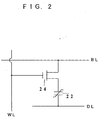
- the ferroelectric capacitor described in the above can be used for a nonvolatile memory when it is combined with a transistor 24 as shown in Fig. 2.
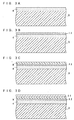
- FIG. 3A, Fig. 3B, Fig. 3C and Fig. 3D are flow charts showing manufacturing processes of a ferroelectric capacitor in an embodiment of the present invention.
- a silicon oxidation layer 4 is formed by carrying out thermal oxidation of a surface of the silicon substrate 2 (Fig. 3A). In this embodiment, the silicon oxidation layer 4 is formed in a thickness of 600 nm.
- a palladium oxide formed on the silicon oxide layer 4 by reactive spattering method using palladium as a target is defined as the lower electrode 12 (Fig. 3B).
- the lower electrode 12 is formed in a thickness of 200 nm.
- a PZT film is formed on the lower electrode 12 as the ferroelectric film 8 by sol-gel method (Fig. 3C).
- a mixed solution of Pb(CH 3 COO) 2 •3H 2 O, Zr(t-OC 4 H 9 ) 4 and Ti(i-OC 3 H 7 ) 4 is used as a starter.
- the mixed solution is dried at a temperature of 150 °C (hereinafter indicated in celsius) after carrying out spin coating, then prebaking is carried out at a temperature of 400 °C for 30 seconds under dried air atmosphere.
- Thermal treatment at a temperature over 700 °C is carried out under O 2 atmosphere after carrying out the processes described in the above for 5 times.
- the ferroelectric film 8 having a thickness of 250 nm is formed.
- the PZT film is formed at a ratio of x equals to 0.52 in PbZr x Ti 1-x O 3 (hereinafter the material is indicated as PZT (52 • 48)).
- a layer made of palladium oxide is formed on the ferroelectric film as the upper electrode 15 by reactive spattering method (Fig. 3D).
- the upper electrode 15 is formed in a thickness of 200 nm.
- the ferroelectric capacitor is completed. Any one of WOx, TiOx, TaOx, IrO 2 , PtO 2 , ReOx, RuOx, OsOx can be used for the palladium oxide.
- the layer made of ferroelectric substance can be formed on any of following conductive layers such as a layer made of W, a Ti layer, a layer made of Ta, an Ir layer, a layer made of Pt, a Ru layer, a layer made of Re and an Os layer or the like. Further, leakage of the ferroelectric substance can be decreased by providing the conductive layer.
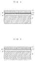
- Fig. 4 shows structure of a ferroelectric capacitor fabricated by another embodiment of the present invention.
- a layer made of titanium (having a thickness of 5 nm) is provided between the lower electrode 12 and the silicon oxidation layer 4 as a contact layer 30.
- palladium oxide and silicon oxide do not contact tightly with each other. So that, there is a probability to cause degradation of ferroelectricity caused by partial delamination of a layer consist of an alloy of palladium oxide and silicon oxide.
- the titanium layer 30 which can be contacted with the silicon oxide layer 4 tightly is provided in this embodiment. So that, the ferroelectricity is improved.
- the titanium layer can be formed by spattering method.
- the titanium layer is used as the contact layer 30 in the embodiment described in the above, any other materials which improve contact can be utilized.
- a layer made of platinum can be used for the contact layer.
- the PZT film is used as the ferroelectric film 8 in the embodiment described in the above, any other materials can be utilized as long as the materials are ferroelectric oxide.
- any other materials can be utilized as long as the materials are ferroelectric oxide.
- Ba 4 Ti 3 O 12 can be used for the ferroelectric film.
- Fig. 5 shows structure of a ferroelectric capacitor fabricated by far another embodiment of the present invention.
- a dielectric layer 90 having high dielectric constant is used for the ferroelectric film 8 in this embodiment.
- the lower electrode 12 made of palladium oxide is provided on the silicon oxide layer 4, and a high dielectric thin film made of SrTiO 3 ,(Sr, Ba)TiO 3 having perovskite structure is formed thereon as the dielectric layer 90.
- ferroelectricity is improved as the same manners as in the embodiment using the ferroelectric substance.
- it is clarified that the advantages offered by using the ferroelectric layer can also be obtained by utilizing the dielectric layer having high dielectric constant.
- Fig. 6 shows structure of a ferroelectric capacitor fabricated by still another embodiment of the present invention.
- the silicon oxidation layer 4, the lower electrode 12, the ferroelectric film (ferroelectric layer) 8 and the upper electrode 15 are provided on the silicon substrate 2.
- the lower electrode 12 is consist of a palladium layer and a palladium oxide layer formed thereon.
- the upper electrode 15 consist of a palladium layer 7 and a palladium oxide layer 9 formed thereon.
- Fig. 7 is an enlarged view of vicinity of the lower electrode 12. Since the palladium oxide layer 11 has columnar crystals, the oxygen contained in the ferroelectric film 8 pass through the palladium oxide layer 11. Another palladium oxide layer 13 is formed on the upper surface of the palladium oxide layer 11 in this embodiment. So that, it is possible to prevent shortage of oxygen contained in the ferroelectric film 8 by forming the palladium oxide layer 13 as described in the above.
- the upper electrode 15 obtains the same advantage which the lower electrode 12 offers as described in the above.
- both of the palladium oxide layers are formed in the lower electrode 12 and the upper electrode 15 respectively in this embodiment, it is possible to obtain a ferroelectric capacitor having an excellent ferroelectricity as well as having less influences of aging. Certain advantage described in the above can be observed when either of the lower electrode 12 or the upper electrode 15 is formed by the structure described in the above.
- Fig. 8A, Fig. 8B, Fig. 8C and Fig. 8D are flow charts showing manufacturing processes of the ferroelectric capacitor described in the above.
- the silicon oxidation layer 4 is formed by carrying out thermal oxidation of a surface of the silicon substrate 2 (Fig. 8A). In this embodiment, the silicon oxidation layer 4 is formed in a thickness of 600 nm.
- the palladium oxide layer 11 is formed on the silicon oxide layer 4 by utilizing palladium as a target (Fig. 8B).
- the palladium oxide layer 13 is formed by carrying out a thermal treatment at a temperature of 800 °C for one minute under O 2 atmosphere.
- the palladium layer 11 and the palladium layer 13 thus formed are defined as the lower electrode 12.
- the lower electrode 12 is formed in a thickness of 200 nm.
- a PZT film is formed on the lower electrode 12 as the ferroelectric film 8 by sol-gel method (Fig. 8C).
- a mixed solution of Pb(CH 3 COO) 2 •3H 2 O, Zr(t-OC 4 H 9 ) 4 and Ti(i-OC 3 H 7 ) 4 is used as a starter.
- the mixed solution is dried at a temperature of 150 °C (hereinafter indicated in celsius) after carrying out spin coating, then prebaking is carried out at a temperature of 400 °C for 30 seconds under dried air atmosphere.
- Thermal treatment at a temperature over 700 °C is carried out under O 2 atmosphere after carrying out the processes described in the above for 5 times.
- the ferroelectric film 8 having a thickness of 250 nm is formed.
- the PZT film is formed at a ratio of x equals to 0.52 in PbZr x Ti 1-x O 3 (hereinafter the material is indicated as PZT (52 • 48)).
- the palladium oxide 7 is formed on the ferroelectric film 8 by spattering method. Then, the palladium oxide layer 9 is formed on a surface of the palladium layer 7 by carrying out a thermal treatment at a temperature of 800 °C for one minute under O 2 atmosphere (Fig. 8D). The palladium layer 7 and the palladium oxide layer 9 thus formed are defined as the upper electrode 15. The upper electrode 15 is formed in a thickness of 200 nm. Thus, the ferroelectric capacitor is completed.
- the process which oxidize a surface of the palladium described in the above can be applied not only to the ferroelectric film, but also to the dielectric layer having high dielectric constant described in the above. So that, the same advantages can be expected.
- a platinum layer 80 (thin film conductive substance) is formed very thinly on the palladium layer 11 as shown in Fig. 9.
- the platinum layer 80 is formed in a thickness of 30 nm.
- a thermal treatment is carried out.
- the platinum layer is not oxidized because the platinum layer 80 exposed on the surface does not react to oxygen.
- leakage of oxygen is shut out by formation of palladium oxygen between crystals of the palladium layer 11 located under the platinum layer 80 as a result of oxidization of the crystals, because the platinum layer 80 is formed thinly. So that, the lower electrode 12 which can shut out leakage of oxygen with maintaining good orientation can be formed.
- the palladium layer 11 which being formed the thin platinum layer 80 and then being oxidized can also be used as the lower electrode 12 by itself.
- the palladium layer 11 can be used as the conductive layer having good orientation in the embodiment of improving orientation by providing a conductive layer (a palladium layer, a platinum layer and the like) having good orientation on the palladium layer formed by spattering.
Abstract
Description
- The present invention relates to a ferroelectric capacitor, more specifically, improvement of ferroelectricity and other characteristics of the capacitor.
- Fig. 10 shows a conventional ferroelectric capacitor. A
silicon oxidation layer 4 is formed on asilicon substrate 2. Alower electrode 6 made of platinum is provided thereon. A PZT (PbZrx Ti1-x O3)film 8 as a ferroelectric layer is formed on thelower electrode 6, and anupper electrode 10 made of platinum is provided thereon. Thus, the ferroelectric capacitor is formed by thelower electrode 6, thePZT film 8 and theupper electrode 10. - The reason to use platinum for the
lower electrode 6 is as follows. ThePZT film 8 must be formed on a layer which can be oriented. Because ferroelectricity of PZT is degraded since the PZT film can not be oriented when the PZT film is formed on a layer made of amorphous. Meanwhile, thelower electrode 6 must be formed under insulation from thesilicon substrate 2. So that, thesilicon oxidation layer 4 is formed on thesilicon substrate 2. Thesilicon oxidation layer 4 is made of amorphous. In general, although a layer formed on an amorphous material becomes nonorientable, a layer made of platinum has a characteristic of becoming orientable even when it is formed on the amorphous material. So that, platinum is used for forming the lower electrode because of the reason described in the above. - However, the conventional ferroelectric capacitor has following problem to be resolved.
- The problems is degradation of ferroelectricity caused by frequent inversion of polarization, aging and leakage of oxygen from the ferroelectric substance (PZT), since platinum has a tendency of allowing oxygen and Pb to pass through it. In other words, there is high probability of leakage of oxygen and Pb contained in the ferroelectric substance through between columnar crystals of platinum shown in Fig. 11. The problem also arises in a capacitor using dielectric substance having high dielectric constant.
- It is an object of the present invention to provide a ferroelectric capacitor having less degradation of ferroelectricity caused by frequent inversion of polarization and aging or a dielectric capacitor maintaining high dielectric constant, both of which resolve the problem described in the above.
- The word "capacitor" in the present invention defines structure providing of electrodes on both sides of an insulator, also it is a concept having the structure stated in the above regardless of using for electric storage.
- In accordance with characteristic of the present invention, a ferroelectric capacitor comprises:
- a lower electrode having an oxidation layer made of any one of following layers, the layers at least including a layer made of WOx, a layer made of TiOx, a layer made of TaOx, a layer made of IrO2, a layer made of PtO2, a layer made of RuOx, a layer made of ReOx, a layer made of PdOx and a layer made of OsOx,
- a dielectric layer composed by either of ferroelectric substance or dielectric substance having a high dielectric constant, the dielectric layer being formed on the lower electrode, and
- an upper electrode formed on the dielectric layer.
-
- In other words, the lower electrode has at least one of following oxidation layers such as the Wox layer, the TiOx layer, the TaOx layer, the IrO2 layer, the PtO2 layer, the RuOx layer, the ReOx layer, the PdOx layer and the OsOx layer. Therefore, it is possible to prevent leakage of oxygen from the dielectric layer as well as suppressing degradation of ferroelectricity caused by aging.
- Also, in accordance with characteristic of the present invention, the lower electrode is composed by forming a conductive layer made of any one of following layers, the layers at least includes a layer made of W, a layer made of Ti, a layer made of Ta, a layer made of Ir, a layer made of Pt, a layer made of Ru, a layer made of Re, a layer made of Pd and a layer made of Os on the oxidation layer, and a ferroelectric layer is formed on the conductive layer.
- Further, in accordance with characteristic of the present invention, the lower electrode is formed on a silicon oxidation layer located on a substrate, and wherein the lower electrode has a contact layer contacted to the silicon oxidation layer.
- That is, one of the following conductive layer such as the W layer, the Ti layer, the Ta layer, the Ir layer, the Pt layer, the Ru layer, the Re layer, the Pd layer and the layer Os layer is provided on the oxidation layer. Then the dielectric layer is formed on the conductive layer. Therefore, leakage current can be decreased.
- Still further, in accordance with characteristic of the present invention, a ferroelectric capacitor comprises:
- a lower electrode,
- a dielectric layer composed by either of ferroelectric substance or dielectric substance having a high dielectric constant, the dielectric layer being formed on the lower electrode, and
- an upper electrode formed on the dielectric layer and having an oxidation layer made of any one of following layers, the layers at least including a layer made of WOx, a layer made of TiOx, a layer made of TaOx, a layer made of IrO2, a layer made of PtO2, a layer made of RuOx, a layer made of ReOx, a layer made of PdOx and a layer made of OsOx.
-
- In other words, the upper electrode has at least one of following conductive layers such as the WOx layer, the TiOx layer, the TaOx layer, the IrO2 layer, the PtO2 layer, the RuOx layer, the ReOx layer, the PdOx layer and the OsOx layer. Therefore, it is possible to prevent leakage of oxygen from the dielectric layer as well as suppressing degradation of ferroelectricity caused by aging.
- In accordance with characteristic of the present invention, the lower electrode is formed on a silicon oxidation layer located on a substrate, and wherein the lower electrode has a contact layer contacted to the silicon oxidation layer.
- Also, in accordance with characteristic of the present invention, a ferroelectric capacitor comprises :
- a lower electrode having an oxidation layer made of any one of following layers, the layers at least including a layer made of WOx, a layer made of TiOx, a layer made of TaOx, a layer made of IrO2, a layer made of PtO2, a layer made of RuOx, a layer made of ReOx, a layer made of PdOx and a layer made of OsOx,
- a dielectric layer composed by either of ferroelectric substance or dielectric substance having a high dielectric constant, the dielectric layer being formed on the lower electrode, and
- an upper electrode having an oxidation layer made of any one of following layers, the layers at least including a layer made of WOx, a layer made of TiOx, a layer made of TaOx, a layer made of IrO2, a layer made of PtO2, a layer made of RuOx, a layer made of ReOx, a layer made of PdOx and a layer made of OsOx.
-
- That is, both of the upper electrode and the lower electrode have at least one of following oxidation layers such as the WOx layer, the TiOx layer, the TaOx layer, the IrO2 layer, the PtO2 layer, the layer RuOx layer, the ReOx layer, the PdOx layer and the OsOx layer. Therefore, it is possible to prevent leakage of oxygen from the dielectric layer as well as suppressing degradation of ferroelectricity caused by aging.
- Further, in accordance with characteristic of the present invention, the lower electrode is composed by forming a conductive layer made of any one of following layers, the layers at least includes a layer made of W, a layer made of Ti, a layer made of Ta, a layer made of Ir, a layer made of Pt, a layer made of Ru, a layer made of Re, a layer made of Pd and a layer made of Os on the oxidation layer, and wherein a ferroelectric layer is formed on the conductive layer.
- Still further, in accordance with characteristic of the present invention, the lower electrode is formed on a silicon oxidation layer located on a substrate, and wherein the lower electrode has a contact layer contacted to the silicon oxidation layer.
- In other words, one of the following conductive layer such as the W layer, the Ti layer, the Ta layer, the Ir layer, the Pt layer, the Ru layer, the Re layer, the Pd layer and the Os layer is provided on the oxidation layer. Then the dielectric layer is formed on the conductive layer. Therefore, leakage current can be decreased.
- In accordance with the present invention, a ferroelectric capacitor which offers excellent ferroelectricity and high-dielectric property can be provided.
- In accordance with characteristic of the present invention, a method for manufacturing a ferroelectric capacitor comprises steps of:
- step for forming any one of following oxidation layers including a layer made of WOx, a layer made of TiOx, a layer made of TaOx, a layer made of IrO2, a layer made of PtO2, a layer made of RuOx, a layer made of ReOx, a layer made of PdOx and a layer made of OsOx on a substrate as a lower electrode by spattering method,
- step for forming either of a ferroelectric film or a dielectric layer having a high dielectric constant on the lower electrode as a dielectric layer, and
- step for forming an upper electrode on the dielectric layer.
-
- Also, in accordance with characteristic of the present invention, a method for manufacturing a ferroelectric capacitor comprises steps of:
- step for forming any one of following layers including a layer made of a layer made of W, a layer made of Ti, a layer made of Ta, a layer made of Ir, a layer made of Pt, a layer made of Ru, a layer made of Re, a layer made of Pd and a layer made of Os on a substrate as a base layer by spattering method,
- step for oxidizing a surface of the base layer,
- step for forming either of a ferroelectric film or a dielectric layer having a high dielectric constant on the base layer as a dielectric layer, a surface of the base layer being oxidized, and
- step for forming an upper electrode on the dielectric layer.
-
- Further, in accordance with characteristic of the present invention, a method for manufacturing a ferroelectric capacitor comprises steps of:
- step for forming either of a ferroelectric film or a dielectric layer having a high dielectric constant on a lower electrode as a dielectric layer, and
- step for forming any one of following oxidation layers including a layer made of WOx, a layer made of TiOx, a layer made of TaOx, a layer made of IrO2, a layer made of PtO2, a layer made of RuOx, a layer made of ReOx, a layer made of PdOx and a layer made of OsOx on the dielectric layer as an upper electrode by spattering method.
-
- Still further, in accordance with characteristic of the present invention a method for manufacturing a ferroelectric capacitor comprises steps of:
- step for forming a lower electrode on a substrate,
- step for forming either of a ferroelectric film or a dielectric layer having a high dielectric constant on the lower electrode as a dielectric layer,
- step for forming any one of following layers including a layer made of a layer made of W, a layer made of Ti, a layer made of Ta, a layer made of Ir, a layer made of Pt, a layer made of Ru, a layer made of Re, a layer made of Pd and a layer made of Os on the dielectric layer as a base layer by spattering method, and
- step for oxidizing a surface of the base layer.
-
- In accordance with characteristic of the present invention, a method for manufacturing a ferroelectric capacitor comprises steps of:
- step for forming any one of following layers including a layer made of a layer made of W, a layer made of Ti, a layer made of Ta, a layer made of Ir, a layer made of Pt, a layer made of Ru, a layer made of Re, a layer made of Pd and a layer made of Os on a substrate as a base layer by spattering method,
- step for forming any one of following layers including a layer made of a layer made of W, a layer made of Ti, a layer made of Ta, a layer made of Ir, a layer made of Pt, a layer made of Ru, a layer made of Re, a layer made of Pd and a layer made of Os on a surface of the base layer as a conductive layer,
- step for oxidizing the conductive layer, a thin conductive layer being formed on a surface of the conductive layer,
- step for forming either of a ferroelectric film or a dielectric layer having a high dielectric constant on the conductive layer as a dielectric layer, the conductive layer being oxidized, and
- step for forming an upper electrode on the dielectric layer.
-
- Also, in accordance with characteristic of the present invention the step of oxidization is carried out within the step for forming the dielectric layer.
- While the novel features of the invention are set forth in a general fashion, both as to organization and content, it will be better understood and appreciated, along with other objections and features thereof, from the following detailed description taken in conjunction with the drawings.
-
- Fig. 1 is a view showing structure of a ferroelectric capacitor in an embodiment of the present invention.
- Fig. 2 is a diagram showing a nonvolatile
memory using a
ferroelectric capacitor 22. - Fig. 3A, Fig. 3B, Fig. 3C and Fig. 3D are flow charts showing manufacturing processes of the ferroelectric capacitor.
- Fig. 4 is a view showing structure of the
ferroelectric capacitor when a
contact layer 30 is provided. - Fig. 5 is a view showing structure of the
ferroelectric capacitor when a
dielectric layer 90 having high dielectric constant is provided. - Fig. 6 is a view showing structure of a ferroelectric capacitor in another embodiment of the present invention.
- Fig. 7 is a view describing a mechanism that how the palladium oxidation layer prevents leakage of oxygen from the ferroelectric film.
- Fig. 8A, Fig. 8B, Fig. 8C and Fig. 8D are flow charts showing manufacturing processes of the ferroelectric capacitor shown in Fig. 1.
- Fig. 9 is a view showing another embodiment of the present invention that caries out oxidization of palladium after forming a thin platinum layer.
- Fig. 10 is a view showing structure of the ferroelectric capacitor in the prior art.
- Fig. 11 is a view showing leakage of oxygen
through the
lower electrode 6 made of platinum. -
- Fig. 1 shows structure of a ferroelectric capacitor fabricated by an embodiment of the present invention. In the ferroelectric capacitor, a
silicon oxidation layer 4, alower electrode 12, a ferroelectric film (ferroelectric layer) 8 and anupper electrode 15 are formed on asilicon substrate 2. Thelower electrode 12 is made of palladium oxide (PdOx), and theupper electrode 15 is also formed by palladium oxide (PdOx). - As shown in Fig. 11 which illustrates the conventional ferroelectric capacitor, oxygen contained in the
ferroelectric film 8 pass through the platinum layer having columnar crystals. Palladium oxide is used for thelower electrode 12 in this embodiment. Since thepalladium oxide layer 12 does not have columnar crystals, it is hard for the oxygen to pass through it. So that, shortage of oxygen in theferroelectric film 8 can be prevented. Shortage of oxygen can also be prevented by theupper electrode 15 which does not have columnar crystals. Thus, ferroelectricity of theferroelectric film 8 is improved. Remarkable improvement of ferroelectricity degradation caused by use of remanent polarization Pr is observed when either of theupper electrode 15 or thelower electrode 12 is made of palladium oxide in comparison with when either one of the electrodes is composed by platinum. - Since both of the
lower electrode 12 and theupper electrode 15 are made of palladium oxide in the embodiment described in the above, the electrodes made of palladium oxide ensures prevention of leakage of oxygen and Pb. Certain prevention of leakage can be expected when either of the electrodes is made by palladium oxide. - The ferroelectric capacitor described in the above can be used for a nonvolatile memory when it is combined with a
transistor 24 as shown in Fig. 2. - Fig. 3A, Fig. 3B, Fig. 3C and Fig. 3D are flow charts showing manufacturing processes of a ferroelectric capacitor in an embodiment of the present invention. A
silicon oxidation layer 4 is formed by carrying out thermal oxidation of a surface of the silicon substrate 2 (Fig. 3A). In this embodiment, thesilicon oxidation layer 4 is formed in a thickness of 600 nm. A palladium oxide formed on thesilicon oxide layer 4 by reactive spattering method using palladium as a target is defined as the lower electrode 12 (Fig. 3B). Thelower electrode 12 is formed in a thickness of 200 nm. - A PZT film is formed on the
lower electrode 12 as theferroelectric film 8 by sol-gel method (Fig. 3C). A mixed solution of Pb(CH3COO)2•3H2O, Zr(t-OC4H9)4 and Ti(i-OC3H7)4 is used as a starter. The mixed solution is dried at a temperature of 150 °C (hereinafter indicated in celsius) after carrying out spin coating, then prebaking is carried out at a temperature of 400 °C for 30 seconds under dried air atmosphere. Thermal treatment at a temperature over 700 °C is carried out under O2 atmosphere after carrying out the processes described in the above for 5 times. Thus, theferroelectric film 8 having a thickness of 250 nm is formed. In this embodiment, the PZT film is formed at a ratio of x equals to 0.52 in PbZr x Ti 1-x O3 (hereinafter the material is indicated as PZT (52 • 48)). - Further, a layer made of palladium oxide is formed on the ferroelectric film as the
upper electrode 15 by reactive spattering method (Fig. 3D). Theupper electrode 15 is formed in a thickness of 200 nm. Thus, the ferroelectric capacitor is completed. Any one of WOx, TiOx, TaOx, IrO2, PtO2, ReOx, RuOx, OsOx can be used for the palladium oxide. - In case of forming a layer made of ferroelectric substance on one of the oxidation layers, orientation of the ferroelectric substance is degraded. In order to maintain the orientation, the layer made of ferroelectric substance can be formed on any of following conductive layers such as a layer made of W, a Ti layer, a layer made of Ta, an Ir layer, a layer made of Pt, a Ru layer, a layer made of Re and an Os layer or the like. Further, leakage of the ferroelectric substance can be decreased by providing the conductive layer.
- Fig. 4 shows structure of a ferroelectric capacitor fabricated by another embodiment of the present invention. In this embodiment, a layer made of titanium (having a thickness of 5 nm) is provided between the
lower electrode 12 and thesilicon oxidation layer 4 as acontact layer 30. In general, palladium oxide and silicon oxide do not contact tightly with each other. So that, there is a probability to cause degradation of ferroelectricity caused by partial delamination of a layer consist of an alloy of palladium oxide and silicon oxide. To resolve the degradation, thetitanium layer 30 which can be contacted with thesilicon oxide layer 4 tightly is provided in this embodiment. So that, the ferroelectricity is improved. The titanium layer can be formed by spattering method. - Although the titanium layer is used as the
contact layer 30 in the embodiment described in the above, any other materials which improve contact can be utilized. For instance, a layer made of platinum can be used for the contact layer. - Though, the PZT film is used as the
ferroelectric film 8 in the embodiment described in the above, any other materials can be utilized as long as the materials are ferroelectric oxide. For instance, Ba4 Ti3O12 can be used for the ferroelectric film. - Fig. 5 shows structure of a ferroelectric capacitor fabricated by far another embodiment of the present invention. A
dielectric layer 90 having high dielectric constant is used for theferroelectric film 8 in this embodiment. Thelower electrode 12 made of palladium oxide is provided on thesilicon oxide layer 4, and a high dielectric thin film made of SrTiO3,(Sr, Ba)TiO3 having perovskite structure is formed thereon as thedielectric layer 90. In this embodiment, ferroelectricity is improved as the same manners as in the embodiment using the ferroelectric substance. In other_words, it is clarified that the advantages offered by using the ferroelectric layer can also be obtained by utilizing the dielectric layer having high dielectric constant. - Fig. 6 shows structure of a ferroelectric capacitor fabricated by still another embodiment of the present invention. In this embodiment, the
silicon oxidation layer 4, thelower electrode 12, the ferroelectric film (ferroelectric layer) 8 and theupper electrode 15 are provided on thesilicon substrate 2. Thelower electrode 12 is consist of a palladium layer and a palladium oxide layer formed thereon. Also, theupper electrode 15 consist of apalladium layer 7 and apalladium oxide layer 9 formed thereon. - Fig. 7 is an enlarged view of vicinity of the
lower electrode 12. Since the palladium oxide layer 11 has columnar crystals, the oxygen contained in theferroelectric film 8 pass through the palladium oxide layer 11. Anotherpalladium oxide layer 13 is formed on the upper surface of the palladium oxide layer 11 in this embodiment. So that, it is possible to prevent shortage of oxygen contained in theferroelectric film 8 by forming thepalladium oxide layer 13 as described in the above. Theupper electrode 15 obtains the same advantage which thelower electrode 12 offers as described in the above. - Since, both of the palladium oxide layers are formed in the
lower electrode 12 and theupper electrode 15 respectively in this embodiment, it is possible to obtain a ferroelectric capacitor having an excellent ferroelectricity as well as having less influences of aging. Certain advantage described in the above can be observed when either of thelower electrode 12 or theupper electrode 15 is formed by the structure described in the above. - Fig. 8A, Fig. 8B, Fig. 8C and Fig. 8D are flow charts showing manufacturing processes of the ferroelectric capacitor described in the above. The
silicon oxidation layer 4 is formed by carrying out thermal oxidation of a surface of the silicon substrate 2 (Fig. 8A). In this embodiment, thesilicon oxidation layer 4 is formed in a thickness of 600 nm. The palladium oxide layer 11 is formed on thesilicon oxide layer 4 by utilizing palladium as a target (Fig. 8B). Thepalladium oxide layer 13 is formed by carrying out a thermal treatment at a temperature of 800 °C for one minute under O2 atmosphere. The palladium layer 11 and thepalladium layer 13 thus formed are defined as thelower electrode 12. Thelower electrode 12 is formed in a thickness of 200 nm. - A PZT film is formed on the
lower electrode 12 as theferroelectric film 8 by sol-gel method (Fig. 8C). A mixed solution of Pb(CH3COO)2•3H2 O, Zr(t-OC4H9)4 and Ti(i-OC3H7)4 is used as a starter. The mixed solution is dried at a temperature of 150 °C (hereinafter indicated in celsius) after carrying out spin coating, then prebaking is carried out at a temperature of 400 °C for 30 seconds under dried air atmosphere. Thermal treatment at a temperature over 700 °C is carried out under O2 atmosphere after carrying out the processes described in the above for 5 times. Thus, theferroelectric film 8 having a thickness of 250 nm is formed. In this embodiment, the PZT film is formed at a ratio of x equals to 0.52 in PbZr x Ti1-x O3 (hereinafter the material is indicated as PZT (52 • 48)). - Further, the
palladium oxide 7 is formed on theferroelectric film 8 by spattering method. Then, thepalladium oxide layer 9 is formed on a surface of thepalladium layer 7 by carrying out a thermal treatment at a temperature of 800 °C for one minute under O2 atmosphere (Fig. 8D). Thepalladium layer 7 and thepalladium oxide layer 9 thus formed are defined as theupper electrode 15. Theupper electrode 15 is formed in a thickness of 200 nm. Thus, the ferroelectric capacitor is completed. - It is also preferable to form the
contact layer 30 in the ferroelectric capacitor as described in Fig. 4. - The process which oxidize a surface of the palladium described in the above can be applied not only to the ferroelectric film, but also to the dielectric layer having high dielectric constant described in the above. So that, the same advantages can be expected.
- As described in the above, though leakage of oxygen can be prevented by oxidizing the surface of the palladium layer, orientation of the ferroelectric layer is degraded by formation of the palladium oxide on its surface. This problem can be resolved by formation of any of following conductive layers on the
palladium oxide layer 13, such as the layer made of W, the Ti layer, the layer made of Ta, the Ir layer, the layer made of Pt, the layer made of Ru, the layer made of Re and the Os layer or the like as already has mentioned. The problem can also be resolved by forming the lower electrode as follows. - At first, a platinum layer 80 (thin film conductive substance) is formed very thinly on the palladium layer 11 as shown in Fig. 9. The platinum layer 80 is formed in a thickness of 30 nm. Thereafter, a thermal treatment is carried out. The platinum layer is not oxidized because the platinum layer 80 exposed on the surface does not react to oxygen. Also, leakage of oxygen is shut out by formation of palladium oxygen between crystals of the palladium layer 11 located under the platinum layer 80 as a result of oxidization of the crystals, because the platinum layer 80 is formed thinly. So that, the
lower electrode 12 which can shut out leakage of oxygen with maintaining good orientation can be formed. - The palladium layer 11 which being formed the thin platinum layer 80 and then being oxidized can also be used as the
lower electrode 12 by itself. The palladium layer 11 can be used as the conductive layer having good orientation in the embodiment of improving orientation by providing a conductive layer (a palladium layer, a platinum layer and the like) having good orientation on the palladium layer formed by spattering. - Also, all of the embodiments described in the above can be applied not only to the ferroelectric capacitor using the ferroelectric film but also to the capacitor using the dielectric layer having high dielectric constant. Exactly the same advantage offered by applying the present invention to the ferroelectric film can be obtained when the present invention is applied to the dielectric layer having high dielectric constant.
- While the invention has been described in its preferred embodiments, it is to be understood that the words which have been used are words of description rather than limitation and that changes within the purview of the appended claims may be made without departing from the true scope and spirit of the invention in its broader aspects.
- This disclosure includes the subject matter set out in the following clauses:
- 1. A ferroelectric capacitor comprising:
- a lower electrode having an oxidation layer made of any one of following layers, the layers at least including a layer made of WOx, a layer made of TiOx, a layer made of TaOx, a layer made of IrO2, a layer made of PtO2, a layer made of RuOx, a layer made of ReOx, a layer made of PdOx and a layer made of OsOx,
- a dielectric layer composed by either of ferroelectric substance or dielectric substance having a high dielectric constant, the dielectric layer being formed on the lower electrode, and
- an upper electrode formed on the dielectric layer.
- 2. A ferroelectric capacitor in accordance
with
clause 1, wherein the lower electrode is composed by forming a conductive layer made of any one of following layers, the layers at least includes a layer made of W, a layer made of Ti, a layer made of Ta, a layer made of Ir, a layer made of Pt, a layer made of Ru, a layer made of Re, a layer made of Pd and a layer made of Os on the oxidation layer, and wherein a ferroelectric layer is formed on the conductive layer. - 3. A ferroelectric capacitor in accordance
with
clause 1 orclause 2, wherein the lower electrode is formed on a silicon oxidation layer located on a substrate, and wherein the lower electrode has a contact layer contacted to the silicon oxidation layer. - 4. A ferroelectric capacitor comprising :
- a lower electrode,
- a dielectric layer composed by either of ferroelectric substance or dielectric substance having a high dielectric constant, the dielectric layer being formed on the lower electrode, and
- an upper electrode formed on the dielectric layer and having an oxidation layer made of any one of following layers, the layers at least including a layer made of WOx, a layer made of TiOx, a layer made of TaOx, a layer made of IrO2, a layer made of PtO2, a layer made of RuOx, a layer made of ReOx, a layer made of PdOx and a layer made of OsOx.
- 5. A ferroelectric capacitor in accordance
with
clause 4, wherein the lower electrode is formed on a silicon oxidation layer located on a substrate, and wherein the lower electrode has a contact layer contacted to the silicon oxidation layer. - 6. A ferroelectric capacitor comprising :
- a lower electrode having an oxidation layer made of any one of following layers, the layers at least including a layer made of WOx, a layer made of TiOx, a layer made of TaOx, a layer made of IrO2, a layer made of PtO2, a layer made of RuOx, a layer made of ReOx, a layer made of PdOx and a layer made of OsOx,
- a dielectric layer composed by either of ferroelectric substance or dielectric substance having a high dielectric constant, the dielectric layer being formed on the lower electrode, and
- an upper electrode having an oxidation layer made of any one of following layers, the layers at least including a layer made of WOx, a layer made of TiOx, a layer made of TaOx, a layer made of IrO2, a layer made of PtO2, a layer made of RuOx, a layer made of ReOx, a layer made of PdOx and a layer made of OsOx.
- 7. A ferroelectric capacitor in accordance
with
clause 6, wherein the lower electrode is composed by forming a conductive layer made of any one of following layers, the layers at least includes a layer made of W, a layer made of Ti, a layer made of Ta, a layer made of Ir, a layer made of Pt, a layer made of Ru, a layer made of Re, a layer made of Pd and a layer made of Os on the oxidation layer, and wherein a ferroelectric layer is formed on the conductive layer. - 8. A ferroelectric capacitor in accordance
with
clause 6 orclause 7, wherein the lower electrode is formed on a silicon oxidation layer located on a substrate, and wherein the lower electrode has a contact layer contacted to the silicon oxidation layer. - 9. A method for manufacturing a ferroelectric
capacitor comprising the steps of:
- step for forming any one of following oxidation layers including a layer made of WOx, a layer made of TiOx, a layer made of TaOx, a layer made of IrO2, a layer made of PtO2, a layer made of RuOx, a layer made of ReOx, a layer made of PdOx and a layer made of OsOx on a substrate as a lower electrode by spattering method,
- step for forming either of a ferroelectric film or a dielectric layer having a high dielectric constant on the lower electrode as a dielectric layer, and
- step for forming an upper electrode on the dielectric layer.
- 10. A method for manufacturing a ferroelectric
capacitor comprising the steps of:
- step for forming any one of following layers including a layer made of a layer made of W, a layer made of Ti, a layer made of Ta, a layer made of Ir, a layer made of Pt, a layer made of Ru, a layer made of Re, a layer made of Pd and a layer made of Os on a substrate as a base layer by spattering method,
- step for oxidizing a surface of the base layer,
- step for forming either of a ferroelectric film or a dielectric layer having a high dielectric constant on the base layer as a dielectric layer, a surface of the base layer being oxidized, and
- step for forming an upper electrode on the dielectric layer.
- 11. A method for manufacturing a ferroelectric
capacitor comprising the steps of:
- step for forming either of a ferroelectric film or a dielectric layer having a high dielectric constant on a lower electrode as a dielectric layer, and
- step for forming any one of following oxidation layers including a layer made of WOx, a layer made of TiOx, a layer made of TaOx, a layer made of IrO2, a layer made of PtO2, a layer made of RuOx, a layer made of ReOx, a layer made of PdOx and a layer made of OsOx on the dielectric layer as an upper electrode by spattering method.
- 12. A method for manufacturing a ferroelectric
capacitor comprising the steps of:
- step for forming a lower electrode on a substrate,
- step for forming either of a ferroelectric film or a dielectric layer having a high dielectric constant on the lower electrode as a dielectric layer,
- step for forming any one of following layers including a layer made of a layer made of W, a layer made of Ti, a layer made of Ta, a layer made of Ir, a layer made of Pt, a layer made of Ru, a layer made of Re, a layer made of Pd and a layer made of Os on the dielectric layer as a base layer by spattering method, and
- step for oxidizing a surface of the base layer.
- 13. A method for manufacturing a ferroelectric
capacitor comprising the steps of:
- step for forming any one of following layers including a layer made of a layer made of W, a layer made of Ti, a layer made of Ta, a layer made of Ir, a layer made of Pt, a layer made of Ru, a layer made of Re, a layer made of Pd and a layer made of Os on a substrate as a base layer by spattering method,
- step for forming any one of following layers including a layer made of a layer made of W, a layer made of Ti, a layer made of Ta, a layer made of Ir, a layer made of Pt, a layer made of Ru, a layer made of Re, a layer made of Pd and a layer made of Os on a surface of the base layer as a conductive layer,
- step for oxidizing the conductive layer, a thin conductive layer being formed on a surface of the conductive layer,
- step for forming either of a ferroelectric film or a dielectric layer having a high dielectric constant on the conductive layer as a dielectric layer, the conductive layer being oxidized, and
- step for forming an upper electrode on the dielectric layer.
- 14. A method for manufacturing a ferroelectric
capacitor in accordance with
clause 10,clause 12 orclause 13, wherein the step of oxidization is carried out within the step for forming the dielectric layer. -
Claims (8)
- A capacitor comprising:a lower electrode made of a material of columnar crystals, wherein the lower electrode includes a layer of at least one of WOx, TiOx, TaOx, IrO2, PtO2, RuOx, ReOx, PdOx and OsOx;an insulative layer of at least one of a ferroelectric substance and a dielectric substance having a high dielectric constant formed on the lower electrode; andan upper electrode formed on the insulative layer.
- The capacitor of claim 1, wherein the lower electrode is composed by forming a conductive layer made of any one of W, Ti, Ta, Ir, Pt, ru, Re, Pd and Os on an oxidation layer, and wherein the insulative layer is formed on the conductive layer.
- The capacitor of claim 1, wherein the lower electrode is formed on a silicon oxidation layer located on a substrate, and has a contact layer in contact with the silicon oxidation layer.
- A capacitor comprising:a lower electrode;an insulative layer formed on the lower electrode and composed of either a ferroelectric substance or a dielectric substance having a high dielectric constant; andan upper electrode formed on the insulative layer, and having a material of columnar crystals and a layer of at least any one of WOx, TiOx, TaOx, IrO2, PtO2, RuOx, ReOx, PdOx and OsOx.
- The capacitor of claim 4, wherein the lower electrode is formed on a silicon oxidation layer located on a substrate and has a contact layer in contact with the silicon oxidation layer.
- A capacitor comprising:a lower electrode having a material of columnar crystals and a layer made of at least one of WOx, TiOx, TaOx, IrO2, PtO2, RuOx, ReOx, PdOx and OsOx;
- The capacitor of claim 6, wherein the lower electrode is composed by forming a conductive layer made of a layer of at least any one W, Ti, Ta, Ir, Pt, Ru, Re, Pd and Os on an oxidation layer, and wherein the insulative layer is formed on the conductive layer.
- The capacitor of claim 6, wherein the lower electrode is formed on a silicon oxidation layer located on a substrate and has a contact layer in contact with the silicon oxidation layer.
Applications Claiming Priority (3)
| Application Number | Priority Date | Filing Date | Title |
|---|---|---|---|
| JP17214295 | 1995-07-07 | ||
| JP17214295A JP3929513B2 (en) | 1995-07-07 | 1995-07-07 | Dielectric capacitor and manufacturing method thereof |
| EP96922252A EP0785579B1 (en) | 1995-07-07 | 1996-07-05 | Dielectric capacitor and process for preparing the same |
Related Parent Applications (1)
| Application Number | Title | Priority Date | Filing Date |
|---|---|---|---|
| EP96922252A Division EP0785579B1 (en) | 1995-07-07 | 1996-07-05 | Dielectric capacitor and process for preparing the same |
Publications (2)
| Publication Number | Publication Date |
|---|---|
| EP1467400A2 true EP1467400A2 (en) | 2004-10-13 |
| EP1467400A3 EP1467400A3 (en) | 2004-10-20 |
Family
ID=15936351
Family Applications (2)
| Application Number | Title | Priority Date | Filing Date |
|---|---|---|---|
| EP96922252A Expired - Lifetime EP0785579B1 (en) | 1995-07-07 | 1996-07-05 | Dielectric capacitor and process for preparing the same |
| EP04076904A Withdrawn EP1467400A3 (en) | 1995-07-07 | 1996-07-05 | Capacitor |
Family Applications Before (1)
| Application Number | Title | Priority Date | Filing Date |
|---|---|---|---|
| EP96922252A Expired - Lifetime EP0785579B1 (en) | 1995-07-07 | 1996-07-05 | Dielectric capacitor and process for preparing the same |
Country Status (8)
| Country | Link |
|---|---|
| US (5) | US6454914B1 (en) |
| EP (2) | EP0785579B1 (en) |
| JP (1) | JP3929513B2 (en) |
| KR (1) | KR100385446B1 (en) |
| CN (1) | CN1085411C (en) |
| CA (1) | CA2197491C (en) |
| DE (1) | DE69633554T2 (en) |
| WO (1) | WO1997003468A1 (en) |
Families Citing this family (36)
| Publication number | Priority date | Publication date | Assignee | Title |
|---|---|---|---|---|
| JP3929513B2 (en) * | 1995-07-07 | 2007-06-13 | ローム株式会社 | Dielectric capacitor and manufacturing method thereof |
| US6699304B1 (en) * | 1997-02-24 | 2004-03-02 | Superior Micropowders, Llc | Palladium-containing particles, method and apparatus of manufacture, palladium-containing devices made therefrom |
| KR100434479B1 (en) * | 1997-07-10 | 2004-09-18 | 삼성전자주식회사 | Highly integrated ferroelectric floating gate ram capable of being operated with one transistor and manufacturing method thereof |
| JP3517876B2 (en) * | 1998-10-14 | 2004-04-12 | セイコーエプソン株式会社 | Ferroelectric thin film element manufacturing method, ink jet recording head, and ink jet printer |
| DE19929307C1 (en) | 1999-06-25 | 2000-11-09 | Siemens Ag | Structured layer, especially a FRAM capacitor lower electrode, is produced by heat treatment to cause layer material migration from a migration region to a target region of a substrate |
| KR100600261B1 (en) * | 1999-12-29 | 2006-07-13 | 주식회사 하이닉스반도체 | Method of forming a capacitor in a semiconductor device |
| US6214661B1 (en) * | 2000-01-21 | 2001-04-10 | Infineon Technologoies North America Corp. | Method to prevent oxygen out-diffusion from BSTO containing micro-electronic device |
| JP4228560B2 (en) * | 2000-11-01 | 2009-02-25 | ソニー株式会社 | Capacitor element and manufacturing method thereof |
| US7378719B2 (en) * | 2000-12-20 | 2008-05-27 | Micron Technology, Inc. | Low leakage MIM capacitor |
| JP4428500B2 (en) | 2001-07-13 | 2010-03-10 | 富士通マイクロエレクトロニクス株式会社 | Capacitor element and manufacturing method thereof |
| US7335552B2 (en) * | 2002-05-15 | 2008-02-26 | Raytheon Company | Electrode for thin film capacitor devices |
| JP2003332539A (en) * | 2002-05-17 | 2003-11-21 | Nec Electronics Corp | Ferroelectric capacitor, manufacturing method thereof, and semiconductor storage device |
| KR100487528B1 (en) * | 2002-06-26 | 2005-05-03 | 삼성전자주식회사 | Ferroelectric capacitor having metal oxide for prohobiting fatigue and method of forming the same |
| JP2004296929A (en) * | 2003-03-27 | 2004-10-21 | Seiko Epson Corp | Process for fabricating ferroelectric capacitor, ferroelectric capacitor, memory element, electronic element, memory device and electronic apparatus |
| US7030463B1 (en) * | 2003-10-01 | 2006-04-18 | University Of Dayton | Tuneable electromagnetic bandgap structures based on high resistivity silicon substrates |
| WO2005043669A1 (en) * | 2003-10-20 | 2005-05-12 | University Of Dayton | Ferroelectric varactors suitable for capacitive shunt switching |
| US20070069264A1 (en) * | 2003-10-20 | 2007-03-29 | Guru Subramanyam | Ferroelectric varactors suitable for capacitive shunt switching and wireless sensing |
| US7719392B2 (en) * | 2003-10-20 | 2010-05-18 | University Of Dayton | Ferroelectric varactors suitable for capacitive shunt switching |
| US7268643B2 (en) * | 2004-01-28 | 2007-09-11 | Paratek Microwave, Inc. | Apparatus, system and method capable of radio frequency switching using tunable dielectric capacitors |
| JP4220459B2 (en) * | 2004-11-22 | 2009-02-04 | 株式会社東芝 | Semiconductor device |
| WO2006131968A1 (en) | 2005-06-09 | 2006-12-14 | Fujitsu Limited | Semiconductor device and method for fabricating same |
| US7345331B1 (en) | 2005-09-23 | 2008-03-18 | United States Of America As Represented By The Secretary Of The Navy | Ferroelectric capacitor circuit for sensing hydrogen gas |
| US8460519B2 (en) * | 2005-10-28 | 2013-06-11 | Applied Materials Inc. | Protective offset sputtering |
| US8454804B2 (en) * | 2005-10-28 | 2013-06-04 | Applied Materials Inc. | Protective offset sputtering |
| US7389675B1 (en) | 2006-05-12 | 2008-06-24 | The United States Of America As Represented By The National Aeronautics And Space Administration | Miniaturized metal (metal alloy)/ PdOx/SiC hydrogen and hydrocarbon gas sensors |
| US8247855B2 (en) * | 2006-09-12 | 2012-08-21 | Texas Instruments Incorporated | Enhanced local interconnects employing ferroelectric electrodes |
| JP2007184623A (en) * | 2007-01-22 | 2007-07-19 | Rohm Co Ltd | Dielectric capacitor |
| WO2008126365A1 (en) * | 2007-03-29 | 2008-10-23 | Panasonic Corporation | Nonvolatile memory device, nonvolatile memory element, and nonvolatile memory element array |
| US7971171B2 (en) * | 2007-07-03 | 2011-06-28 | International Business Machines Corporation | Method and system for electromigration analysis on signal wiring |
| US7922975B2 (en) * | 2008-07-14 | 2011-04-12 | University Of Dayton | Resonant sensor capable of wireless interrogation |
| JP5347381B2 (en) * | 2008-08-28 | 2013-11-20 | 富士通セミコンダクター株式会社 | Manufacturing method of semiconductor device |
| US20100096678A1 (en) * | 2008-10-20 | 2010-04-22 | University Of Dayton | Nanostructured barium strontium titanate (bst) thin-film varactors on sapphire |
| CN102157262B (en) * | 2011-03-10 | 2012-09-05 | 苏州大学 | Method for preparing capacitor with Ta205 thin film as dielectric film |
| US9000866B2 (en) | 2012-06-26 | 2015-04-07 | University Of Dayton | Varactor shunt switches with parallel capacitor architecture |
| RU2550090C2 (en) * | 2013-03-06 | 2015-05-10 | Открытое Акционерное общество "Научно-исследовательский институт "Гириконд" | Thin-film ferroelectric capacitor |
| CN113278935B (en) * | 2021-05-07 | 2022-12-09 | 昆明贵研新材料科技有限公司 | Platinum oxide electrode and preparation method and application thereof |
Citations (1)
| Publication number | Priority date | Publication date | Assignee | Title |
|---|---|---|---|---|
| EP0409018A2 (en) * | 1989-07-17 | 1991-01-23 | National Semiconductor Corporation | Electrodes for electrical ceramic oxide devices |
Family Cites Families (27)
| Publication number | Priority date | Publication date | Assignee | Title |
|---|---|---|---|---|
| US3616400A (en) * | 1968-03-25 | 1971-10-26 | Matsushita Electric Ind Co Ltd | Method of making thin film capacitor |
| US5214300A (en) * | 1970-09-28 | 1993-05-25 | Ramtron Corporation | Monolithic semiconductor integrated circuit ferroelectric memory device |
| JPS4870855A (en) * | 1971-12-29 | 1973-09-26 | ||
| US3969197A (en) * | 1974-02-08 | 1976-07-13 | Texas Instruments Incorporated | Method for fabricating a thin film capacitor |
| DE2513858C3 (en) * | 1975-03-27 | 1981-08-06 | Siemens AG, 1000 Berlin und 8000 München | Process for the production of a tantalum thin film capacitor |
| US4038167A (en) * | 1976-02-09 | 1977-07-26 | Corning Glass Works | Method of forming a thin film capacitor |
| US5005102A (en) * | 1989-06-20 | 1991-04-02 | Ramtron Corporation | Multilayer electrodes for integrated circuit capacitors |
| JPH0712074B2 (en) | 1990-03-01 | 1995-02-08 | 日本電気株式会社 | Thin film capacitor and manufacturing method thereof |
| US5122923A (en) * | 1989-08-30 | 1992-06-16 | Nec Corporation | Thin-film capacitors and process for manufacturing the same |
| EP0468758B1 (en) * | 1990-07-24 | 1997-03-26 | Semiconductor Energy Laboratory Co., Ltd. | Method of forming insulating films, capacitances, and semiconductor devices |
| US5262920A (en) * | 1991-05-16 | 1993-11-16 | Nec Corporation | Thin film capacitor |
| US5142437A (en) | 1991-06-13 | 1992-08-25 | Ramtron Corporation | Conducting electrode layers for ferroelectric capacitors in integrated circuits and method |
| US5164808A (en) * | 1991-08-09 | 1992-11-17 | Radiant Technologies | Platinum electrode structure for use in conjunction with ferroelectric materials |
| US5723361A (en) * | 1991-12-13 | 1998-03-03 | Symetrix Corporation | Thin films of ABO3 with excess A-site and B-site modifiers and method of fabricating integrated circuits with same |
| US5191510A (en) * | 1992-04-29 | 1993-03-02 | Ramtron International Corporation | Use of palladium as an adhesion layer and as an electrode in ferroelectric memory devices |
| JP3407204B2 (en) * | 1992-07-23 | 2003-05-19 | オリンパス光学工業株式会社 | Ferroelectric integrated circuit and method of manufacturing the same |
| US5348894A (en) * | 1993-01-27 | 1994-09-20 | Texas Instruments Incorporated | Method of forming electrical connections to high dielectric constant materials |
| JP2629586B2 (en) * | 1993-12-16 | 1997-07-09 | 日本電気株式会社 | Semiconductor device and method of manufacturing the same |
| US6052271A (en) | 1994-01-13 | 2000-04-18 | Rohm Co., Ltd. | Ferroelectric capacitor including an iridium oxide layer in the lower electrode |
| JP3461398B2 (en) | 1994-01-13 | 2003-10-27 | ローム株式会社 | Dielectric capacitor and method of manufacturing the same |
| JPH088403A (en) * | 1994-06-17 | 1996-01-12 | Sharp Corp | Substrate covered with ferroelectric crystal thin film ferroelectric thin film element including the same, and method of manufacturing the ferroelectric thin film element |
| DE4421007A1 (en) * | 1994-06-18 | 1995-12-21 | Philips Patentverwaltung | Electronic component and method for its production |
| JP2755174B2 (en) * | 1994-06-21 | 1998-05-20 | 日本電気株式会社 | Ferroelectric capacitor and memory cell structure |
| JP3188361B2 (en) * | 1994-06-27 | 2001-07-16 | ペルメレック電極株式会社 | Chrome plating method |
| JPH08162619A (en) * | 1994-12-09 | 1996-06-21 | Hitachi Ltd | Semiconductor device and manufacture thereof |
| US5753945A (en) * | 1995-06-29 | 1998-05-19 | Northern Telecom Limited | Integrated circuit structure comprising a zirconium titanium oxide barrier layer and method of forming a zirconium titanium oxide barrier layer |
| JP3929513B2 (en) * | 1995-07-07 | 2007-06-13 | ローム株式会社 | Dielectric capacitor and manufacturing method thereof |
-
1995
- 1995-07-07 JP JP17214295A patent/JP3929513B2/en not_active Expired - Fee Related
-
1996
- 1996-07-05 KR KR1019960706383A patent/KR100385446B1/en not_active IP Right Cessation
- 1996-07-05 EP EP96922252A patent/EP0785579B1/en not_active Expired - Lifetime
- 1996-07-05 WO PCT/JP1996/001883 patent/WO1997003468A1/en active IP Right Grant
- 1996-07-05 CA CA002197491A patent/CA2197491C/en not_active Expired - Fee Related
- 1996-07-05 EP EP04076904A patent/EP1467400A3/en not_active Withdrawn
- 1996-07-05 CN CN96190228A patent/CN1085411C/en not_active Expired - Fee Related
- 1996-07-05 DE DE69633554T patent/DE69633554T2/en not_active Expired - Fee Related
-
1997
- 1997-02-20 US US08/812,059 patent/US6454914B1/en not_active Expired - Lifetime
-
2002
- 2002-08-08 US US10/215,844 patent/US6693791B2/en not_active Expired - Lifetime
-
2003
- 2003-08-29 US US10/651,435 patent/US6873517B2/en not_active Expired - Fee Related
-
2004
- 2004-12-16 US US11/015,082 patent/US7057874B2/en not_active Expired - Fee Related
-
2006
- 2006-04-12 US US11/279,495 patent/US7443649B2/en not_active Expired - Fee Related
Patent Citations (1)
| Publication number | Priority date | Publication date | Assignee | Title |
|---|---|---|---|---|
| EP0409018A2 (en) * | 1989-07-17 | 1991-01-23 | National Semiconductor Corporation | Electrodes for electrical ceramic oxide devices |
Non-Patent Citations (3)
| Title |
|---|
| AMANUMA K ET AL: "Ferroelectric properties of sol-gel derived Pb(Zr,Ti)O/sub 3/ thin films" JPN. J. APPL. PHYS. 1, REGUL. PAP. SHORT NOTES (JAPAN), JAPANESE JOURNAL OF APPLIED PHYSICS, PART 1 (REGULAR PAPERS & SHORT NOTES), SEPT. 1993, JAPAN, vol. 32, no. 9B, September 1993 (1993-09), pages 4150-4153, XP001199583 ISSN: 0021-4922 * |
| FOX G R ET AL: "Pt/Ti/SiO/sub 2//Si substrates" J. MATER. RES. (USA), JOURNAL OF MATERIALS RESEARCH, JUNE 1995, MATER. RES. SOC, USA, vol. 10, no. 6, June 1995 (1995-06), pages 1508-1515, XP008034566 ISSN: 0884-2914 * |
| NAKAO Y ET AL: "Study on ferroelectric thin films for application to NDRO non-volatile memories" INTEGR. FERROELECTR. (UK), INTEGRATED FERROELECTRICS, 1995, UK, vol. 6, no. 1-4, 14 March 1994 (1994-03-14), pages 23-34, XP001001236 SIXTH INTERNATIONAL SYMPOSIUM ON INTEGRATED FERROELECTRICS, MONTEREY, CA, USA ISSN: 1058-4587 * |
Also Published As
| Publication number | Publication date |
|---|---|
| KR970703049A (en) | 1997-06-10 |
| CN1085411C (en) | 2002-05-22 |
| CN1155943A (en) | 1997-07-30 |
| DE69633554D1 (en) | 2004-11-11 |
| EP0785579B1 (en) | 2004-10-06 |
| EP1467400A3 (en) | 2004-10-20 |
| JP3929513B2 (en) | 2007-06-13 |
| US20060170021A1 (en) | 2006-08-03 |
| US20040036105A1 (en) | 2004-02-26 |
| CA2197491C (en) | 2002-01-01 |
| US6454914B1 (en) | 2002-09-24 |
| CA2197491A1 (en) | 1997-01-30 |
| US20050098819A1 (en) | 2005-05-12 |
| US6693791B2 (en) | 2004-02-17 |
| JPH0922829A (en) | 1997-01-21 |
| DE69633554T2 (en) | 2005-10-13 |
| US6873517B2 (en) | 2005-03-29 |
| US7057874B2 (en) | 2006-06-06 |
| EP0785579A4 (en) | 1998-10-14 |
| EP0785579A1 (en) | 1997-07-23 |
| KR100385446B1 (en) | 2004-09-08 |
| US20020189933A1 (en) | 2002-12-19 |
| US7443649B2 (en) | 2008-10-28 |
| WO1997003468A1 (en) | 1997-01-30 |
Similar Documents
| Publication | Publication Date | Title |
|---|---|---|
| US7443649B2 (en) | Ferroelectric capacitor | |
| JP3319994B2 (en) | Semiconductor storage element | |
| KR100288025B1 (en) | Semiconductor memory device and manufacturing method thereof | |
| JP3412051B2 (en) | Capacitor | |
| US20020021546A1 (en) | Ferroelectric capacitor and a mehtod for manufacturing thereof | |
| US6274454B1 (en) | Method for fabricating dielectric capacitor | |
| KR100430324B1 (en) | Capacitor electrode structure | |
| JP3349612B2 (en) | Dielectric capacitor and method of manufacturing the same | |
| KR100243298B1 (en) | Method for forming the capacitor of a semiconductor device | |
| JP2001237402A (en) | Structured metal oxide containing layer, and method of manufacturing semiconductor structure element | |
| JP3981142B2 (en) | Ferroelectric capacitor and manufacturing method thereof | |
| US7026674B2 (en) | Semiconductor memory device and manufacturing method thereof | |
| KR100277939B1 (en) | bottom electrode of capacitor with ferroelectric | |
| KR100288688B1 (en) | Manufacturing Method of Semiconductor Memory Device | |
| JPH07263635A (en) | Capacitor and semiconductor device | |
| JPH10229169A (en) | Ferroelectric memory element, manufacture thereof and integrated circuit | |
| JPH11233386A (en) | Capacitor and manufacture thereof |
Legal Events
| Date | Code | Title | Description |
|---|---|---|---|
| PUAI | Public reference made under article 153(3) epc to a published international application that has entered the european phase |
Free format text: ORIGINAL CODE: 0009012 |
|
| PUAL | Search report despatched |
Free format text: ORIGINAL CODE: 0009013 |
|
| AC | Divisional application: reference to earlier application |
Ref document number: 0785579 Country of ref document: EP Kind code of ref document: P |
|
| AK | Designated contracting states |
Kind code of ref document: A2 Designated state(s): DE FR GB IT NL |
|
| AK | Designated contracting states |
Kind code of ref document: A3 Designated state(s): DE FR GB IT NL |
|
| RIC1 | Information provided on ipc code assigned before grant |
Ipc: 7H 01L 27/108 B Ipc: 7H 01L 21/3205 A Ipc: 7H 01L 21/8242 B |
|
| 17P | Request for examination filed |
Effective date: 20050412 |
|
| AKX | Designation fees paid |
Designated state(s): DE FR GB IT NL |
|
| 17Q | First examination report despatched |
Effective date: 20071022 |
|
| STAA | Information on the status of an ep patent application or granted ep patent |
Free format text: STATUS: THE APPLICATION IS DEEMED TO BE WITHDRAWN |
|
| 18D | Application deemed to be withdrawn |
Effective date: 20100202 |