EP1467400A2 - Kondensator - Google Patents
Kondensator Download PDFInfo
- Publication number
- EP1467400A2 EP1467400A2 EP04076904A EP04076904A EP1467400A2 EP 1467400 A2 EP1467400 A2 EP 1467400A2 EP 04076904 A EP04076904 A EP 04076904A EP 04076904 A EP04076904 A EP 04076904A EP 1467400 A2 EP1467400 A2 EP 1467400A2
- Authority
- EP
- European Patent Office
- Prior art keywords
- layer
- layer made
- lower electrode
- ferroelectric
- capacitor
- Prior art date
- Legal status (The legal status is an assumption and is not a legal conclusion. Google has not performed a legal analysis and makes no representation as to the accuracy of the status listed.)
- Withdrawn
Links
Images


Classifications
-
- H—ELECTRICITY
- H10—SEMICONDUCTOR DEVICES; ELECTRIC SOLID-STATE DEVICES NOT OTHERWISE PROVIDED FOR
- H10D—INORGANIC ELECTRIC SEMICONDUCTOR DEVICES
- H10D1/00—Resistors, capacitors or inductors
- H10D1/60—Capacitors
- H10D1/62—Capacitors having potential barriers
-
- H—ELECTRICITY
- H10—SEMICONDUCTOR DEVICES; ELECTRIC SOLID-STATE DEVICES NOT OTHERWISE PROVIDED FOR
- H10P—GENERIC PROCESSES OR APPARATUS FOR THE MANUFACTURE OR TREATMENT OF DEVICES COVERED BY CLASS H10
- H10P14/00—Formation of materials, e.g. in the shape of layers or pillars
- H10P14/40—Formation of materials, e.g. in the shape of layers or pillars of conductive or resistive materials
- H10P14/412—Deposition of metallic or metal-silicide materials
-
- H—ELECTRICITY
- H10—SEMICONDUCTOR DEVICES; ELECTRIC SOLID-STATE DEVICES NOT OTHERWISE PROVIDED FOR
- H10D—INORGANIC ELECTRIC SEMICONDUCTOR DEVICES
- H10D1/00—Resistors, capacitors or inductors
- H10D1/60—Capacitors
- H10D1/68—Capacitors having no potential barriers
- H10D1/682—Capacitors having no potential barriers having dielectrics comprising perovskite structures
- H10D1/684—Capacitors having no potential barriers having dielectrics comprising perovskite structures the dielectrics comprising multiple layers, e.g. comprising buffer layers, seed layers or gradient layers
-
- H—ELECTRICITY
- H10—SEMICONDUCTOR DEVICES; ELECTRIC SOLID-STATE DEVICES NOT OTHERWISE PROVIDED FOR
- H10D—INORGANIC ELECTRIC SEMICONDUCTOR DEVICES
- H10D1/00—Resistors, capacitors or inductors
- H10D1/60—Capacitors
- H10D1/68—Capacitors having no potential barriers
- H10D1/692—Electrodes
-
- H—ELECTRICITY
- H10—SEMICONDUCTOR DEVICES; ELECTRIC SOLID-STATE DEVICES NOT OTHERWISE PROVIDED FOR
- H10D—INORGANIC ELECTRIC SEMICONDUCTOR DEVICES
- H10D1/00—Resistors, capacitors or inductors
- H10D1/60—Capacitors
- H10D1/68—Capacitors having no potential barriers
- H10D1/692—Electrodes
- H10D1/694—Electrodes comprising noble metals or noble metal oxides
-
- H—ELECTRICITY
- H10—SEMICONDUCTOR DEVICES; ELECTRIC SOLID-STATE DEVICES NOT OTHERWISE PROVIDED FOR
- H10D—INORGANIC ELECTRIC SEMICONDUCTOR DEVICES
- H10D1/00—Resistors, capacitors or inductors
- H10D1/60—Capacitors
- H10D1/68—Capacitors having no potential barriers
- H10D1/692—Electrodes
- H10D1/696—Electrodes comprising multiple layers, e.g. comprising a barrier layer and a metal layer
-
- H—ELECTRICITY
- H10—SEMICONDUCTOR DEVICES; ELECTRIC SOLID-STATE DEVICES NOT OTHERWISE PROVIDED FOR
- H10D—INORGANIC ELECTRIC SEMICONDUCTOR DEVICES
- H10D84/00—Integrated devices formed in or on semiconductor substrates that comprise only semiconducting layers, e.g. on Si wafers or on GaAs-on-Si wafers
- H10D84/201—Integrated devices formed in or on semiconductor substrates that comprise only semiconducting layers, e.g. on Si wafers or on GaAs-on-Si wafers characterised by the integration of only components covered by H10D1/00 or H10D8/00, e.g. RLC circuits
- H10D84/204—Integrated devices formed in or on semiconductor substrates that comprise only semiconducting layers, e.g. on Si wafers or on GaAs-on-Si wafers characterised by the integration of only components covered by H10D1/00 or H10D8/00, e.g. RLC circuits of combinations of diodes or capacitors or resistors
- H10D84/212—Integrated devices formed in or on semiconductor substrates that comprise only semiconducting layers, e.g. on Si wafers or on GaAs-on-Si wafers characterised by the integration of only components covered by H10D1/00 or H10D8/00, e.g. RLC circuits of combinations of diodes or capacitors or resistors of only capacitors
-
- H—ELECTRICITY
- H10—SEMICONDUCTOR DEVICES; ELECTRIC SOLID-STATE DEVICES NOT OTHERWISE PROVIDED FOR
- H10D—INORGANIC ELECTRIC SEMICONDUCTOR DEVICES
- H10D1/00—Resistors, capacitors or inductors
- H10D1/60—Capacitors
- H10D1/68—Capacitors having no potential barriers
- H10D1/682—Capacitors having no potential barriers having dielectrics comprising perovskite structures
-
- H—ELECTRICITY
- H10—SEMICONDUCTOR DEVICES; ELECTRIC SOLID-STATE DEVICES NOT OTHERWISE PROVIDED FOR
- H10W—GENERIC PACKAGES, INTERCONNECTIONS, CONNECTORS OR OTHER CONSTRUCTIONAL DETAILS OF DEVICES COVERED BY CLASS H10
- H10W20/00—Interconnections in chips, wafers or substrates
- H10W20/01—Manufacture or treatment
- H10W20/031—Manufacture or treatment of conductive parts of the interconnections
- H10W20/032—Manufacture or treatment of conductive parts of the interconnections of conductive barrier, adhesion or liner layers
Definitions
- the present invention relates to a ferroelectric capacitor, more specifically, improvement of ferroelectricity and other characteristics of the capacitor.
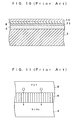
- Fig. 10 shows a conventional ferroelectric capacitor.
- a silicon oxidation layer 4 is formed on a silicon substrate 2.
- a lower electrode 6 made of platinum is provided thereon.
- a PZT (PbZr x Ti 1-x O 3 ) film 8 as a ferroelectric layer is formed on the lower electrode 6, and an upper electrode 10 made of platinum is provided thereon.
- the ferroelectric capacitor is formed by the lower electrode 6, the PZT film 8 and the upper electrode 10.
- the reason to use platinum for the lower electrode 6 is as follows.
- the PZT film 8 must be formed on a layer which can be oriented. Because ferroelectricity of PZT is degraded since the PZT film can not be oriented when the PZT film is formed on a layer made of amorphous.
- the lower electrode 6 must be formed under insulation from the silicon substrate 2. So that, the silicon oxidation layer 4 is formed on the silicon substrate 2.
- the silicon oxidation layer 4 is made of amorphous. In general, although a layer formed on an amorphous material becomes nonorientable, a layer made of platinum has a characteristic of becoming orientable even when it is formed on the amorphous material. So that, platinum is used for forming the lower electrode because of the reason described in the above.
- the conventional ferroelectric capacitor has following problem to be resolved.
- the problems is degradation of ferroelectricity caused by frequent inversion of polarization, aging and leakage of oxygen from the ferroelectric substance (PZT), since platinum has a tendency of allowing oxygen and Pb to pass through it. In other words, there is high probability of leakage of oxygen and Pb contained in the ferroelectric substance through between columnar crystals of platinum shown in Fig. 11.
- the problem also arises in a capacitor using dielectric substance having high dielectric constant.
- capacitor in the present invention defines structure providing of electrodes on both sides of an insulator, also it is a concept having the structure stated in the above regardless of using for electric storage.
- a ferroelectric capacitor comprises:
- the lower electrode has at least one of following oxidation layers such as the Wox layer, the TiOx layer, the TaOx layer, the IrO 2 layer, the PtO 2 layer, the RuOx layer, the ReOx layer, the PdOx layer and the OsOx layer. Therefore, it is possible to prevent leakage of oxygen from the dielectric layer as well as suppressing degradation of ferroelectricity caused by aging.
- the lower electrode is composed by forming a conductive layer made of any one of following layers, the layers at least includes a layer made of W, a layer made of Ti, a layer made of Ta, a layer made of Ir, a layer made of Pt, a layer made of Ru, a layer made of Re, a layer made of Pd and a layer made of Os on the oxidation layer, and a ferroelectric layer is formed on the conductive layer.
- the lower electrode is formed on a silicon oxidation layer located on a substrate, and wherein the lower electrode has a contact layer contacted to the silicon oxidation layer.
- one of the following conductive layer such as the W layer, the Ti layer, the Ta layer, the Ir layer, the Pt layer, the Ru layer, the Re layer, the Pd layer and the layer Os layer is provided on the oxidation layer. Then the dielectric layer is formed on the conductive layer. Therefore, leakage current can be decreased.
- a ferroelectric capacitor comprises:
- the upper electrode has at least one of following conductive layers such as the WOx layer, the TiOx layer, the TaOx layer, the IrO 2 layer, the PtO 2 layer, the RuOx layer, the ReOx layer, the PdOx layer and the OsOx layer. Therefore, it is possible to prevent leakage of oxygen from the dielectric layer as well as suppressing degradation of ferroelectricity caused by aging.
- the lower electrode is formed on a silicon oxidation layer located on a substrate, and wherein the lower electrode has a contact layer contacted to the silicon oxidation layer.
- a ferroelectric capacitor comprises :
- both of the upper electrode and the lower electrode have at least one of following oxidation layers such as the WOx layer, the TiOx layer, the TaOx layer, the IrO 2 layer, the PtO 2 layer, the layer RuOx layer, the ReOx layer, the PdOx layer and the OsOx layer. Therefore, it is possible to prevent leakage of oxygen from the dielectric layer as well as suppressing degradation of ferroelectricity caused by aging.
- the lower electrode is composed by forming a conductive layer made of any one of following layers, the layers at least includes a layer made of W, a layer made of Ti, a layer made of Ta, a layer made of Ir, a layer made of Pt, a layer made of Ru, a layer made of Re, a layer made of Pd and a layer made of Os on the oxidation layer, and wherein a ferroelectric layer is formed on the conductive layer.
- the lower electrode is formed on a silicon oxidation layer located on a substrate, and wherein the lower electrode has a contact layer contacted to the silicon oxidation layer.
- one of the following conductive layer such as the W layer, the Ti layer, the Ta layer, the Ir layer, the Pt layer, the Ru layer, the Re layer, the Pd layer and the Os layer is provided on the oxidation layer. Then the dielectric layer is formed on the conductive layer. Therefore, leakage current can be decreased.
- a ferroelectric capacitor which offers excellent ferroelectricity and high-dielectric property can be provided.
- a method for manufacturing a ferroelectric capacitor comprises steps of:
- a method for manufacturing a ferroelectric capacitor comprises steps of:
- a method for manufacturing a ferroelectric capacitor comprises steps of:
- a method for manufacturing a ferroelectric capacitor comprises steps of:
- a method for manufacturing a ferroelectric capacitor comprises steps of:
- the step of oxidization is carried out within the step for forming the dielectric layer.
- Fig. 1 shows structure of a ferroelectric capacitor fabricated by an embodiment of the present invention.
- a silicon oxidation layer 4 a lower electrode 12, a ferroelectric film (ferroelectric layer) 8 and an upper electrode 15 are formed on a silicon substrate 2.
- the lower electrode 12 is made of palladium oxide (PdOx), and the upper electrode 15 is also formed by palladium oxide (PdOx).
- Fig. 11 which illustrates the conventional ferroelectric capacitor
- oxygen contained in the ferroelectric film 8 pass through the platinum layer having columnar crystals.
- Palladium oxide is used for the lower electrode 12 in this embodiment. Since the palladium oxide layer 12 does not have columnar crystals, it is hard for the oxygen to pass through it. So that, shortage of oxygen in the ferroelectric film 8 can be prevented. Shortage of oxygen can also be prevented by the upper electrode 15 which does not have columnar crystals. Thus, ferroelectricity of the ferroelectric film 8 is improved. Remarkable improvement of ferroelectricity degradation caused by use of remanent polarization Pr is observed when either of the upper electrode 15 or the lower electrode 12 is made of palladium oxide in comparison with when either one of the electrodes is composed by platinum.
- the electrodes made of palladium oxide ensures prevention of leakage of oxygen and Pb. Certain prevention of leakage can be expected when either of the electrodes is made by palladium oxide.
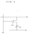
- the ferroelectric capacitor described in the above can be used for a nonvolatile memory when it is combined with a transistor 24 as shown in Fig. 2.
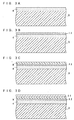
- FIG. 3A, Fig. 3B, Fig. 3C and Fig. 3D are flow charts showing manufacturing processes of a ferroelectric capacitor in an embodiment of the present invention.
- a silicon oxidation layer 4 is formed by carrying out thermal oxidation of a surface of the silicon substrate 2 (Fig. 3A). In this embodiment, the silicon oxidation layer 4 is formed in a thickness of 600 nm.
- a palladium oxide formed on the silicon oxide layer 4 by reactive spattering method using palladium as a target is defined as the lower electrode 12 (Fig. 3B).
- the lower electrode 12 is formed in a thickness of 200 nm.
- a PZT film is formed on the lower electrode 12 as the ferroelectric film 8 by sol-gel method (Fig. 3C).
- a mixed solution of Pb(CH 3 COO) 2 •3H 2 O, Zr(t-OC 4 H 9 ) 4 and Ti(i-OC 3 H 7 ) 4 is used as a starter.
- the mixed solution is dried at a temperature of 150 °C (hereinafter indicated in celsius) after carrying out spin coating, then prebaking is carried out at a temperature of 400 °C for 30 seconds under dried air atmosphere.
- Thermal treatment at a temperature over 700 °C is carried out under O 2 atmosphere after carrying out the processes described in the above for 5 times.
- the ferroelectric film 8 having a thickness of 250 nm is formed.
- the PZT film is formed at a ratio of x equals to 0.52 in PbZr x Ti 1-x O 3 (hereinafter the material is indicated as PZT (52 • 48)).
- a layer made of palladium oxide is formed on the ferroelectric film as the upper electrode 15 by reactive spattering method (Fig. 3D).
- the upper electrode 15 is formed in a thickness of 200 nm.
- the ferroelectric capacitor is completed. Any one of WOx, TiOx, TaOx, IrO 2 , PtO 2 , ReOx, RuOx, OsOx can be used for the palladium oxide.
- the layer made of ferroelectric substance can be formed on any of following conductive layers such as a layer made of W, a Ti layer, a layer made of Ta, an Ir layer, a layer made of Pt, a Ru layer, a layer made of Re and an Os layer or the like. Further, leakage of the ferroelectric substance can be decreased by providing the conductive layer.
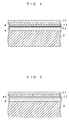
- Fig. 4 shows structure of a ferroelectric capacitor fabricated by another embodiment of the present invention.
- a layer made of titanium (having a thickness of 5 nm) is provided between the lower electrode 12 and the silicon oxidation layer 4 as a contact layer 30.
- palladium oxide and silicon oxide do not contact tightly with each other. So that, there is a probability to cause degradation of ferroelectricity caused by partial delamination of a layer consist of an alloy of palladium oxide and silicon oxide.
- the titanium layer 30 which can be contacted with the silicon oxide layer 4 tightly is provided in this embodiment. So that, the ferroelectricity is improved.
- the titanium layer can be formed by spattering method.
- the titanium layer is used as the contact layer 30 in the embodiment described in the above, any other materials which improve contact can be utilized.
- a layer made of platinum can be used for the contact layer.
- the PZT film is used as the ferroelectric film 8 in the embodiment described in the above, any other materials can be utilized as long as the materials are ferroelectric oxide.
- any other materials can be utilized as long as the materials are ferroelectric oxide.
- Ba 4 Ti 3 O 12 can be used for the ferroelectric film.
- Fig. 5 shows structure of a ferroelectric capacitor fabricated by far another embodiment of the present invention.
- a dielectric layer 90 having high dielectric constant is used for the ferroelectric film 8 in this embodiment.
- the lower electrode 12 made of palladium oxide is provided on the silicon oxide layer 4, and a high dielectric thin film made of SrTiO 3 ,(Sr, Ba)TiO 3 having perovskite structure is formed thereon as the dielectric layer 90.
- ferroelectricity is improved as the same manners as in the embodiment using the ferroelectric substance.
- it is clarified that the advantages offered by using the ferroelectric layer can also be obtained by utilizing the dielectric layer having high dielectric constant.
- Fig. 6 shows structure of a ferroelectric capacitor fabricated by still another embodiment of the present invention.
- the silicon oxidation layer 4, the lower electrode 12, the ferroelectric film (ferroelectric layer) 8 and the upper electrode 15 are provided on the silicon substrate 2.
- the lower electrode 12 is consist of a palladium layer and a palladium oxide layer formed thereon.
- the upper electrode 15 consist of a palladium layer 7 and a palladium oxide layer 9 formed thereon.
- Fig. 7 is an enlarged view of vicinity of the lower electrode 12. Since the palladium oxide layer 11 has columnar crystals, the oxygen contained in the ferroelectric film 8 pass through the palladium oxide layer 11. Another palladium oxide layer 13 is formed on the upper surface of the palladium oxide layer 11 in this embodiment. So that, it is possible to prevent shortage of oxygen contained in the ferroelectric film 8 by forming the palladium oxide layer 13 as described in the above.
- the upper electrode 15 obtains the same advantage which the lower electrode 12 offers as described in the above.
- both of the palladium oxide layers are formed in the lower electrode 12 and the upper electrode 15 respectively in this embodiment, it is possible to obtain a ferroelectric capacitor having an excellent ferroelectricity as well as having less influences of aging. Certain advantage described in the above can be observed when either of the lower electrode 12 or the upper electrode 15 is formed by the structure described in the above.
- Fig. 8A, Fig. 8B, Fig. 8C and Fig. 8D are flow charts showing manufacturing processes of the ferroelectric capacitor described in the above.
- the silicon oxidation layer 4 is formed by carrying out thermal oxidation of a surface of the silicon substrate 2 (Fig. 8A). In this embodiment, the silicon oxidation layer 4 is formed in a thickness of 600 nm.
- the palladium oxide layer 11 is formed on the silicon oxide layer 4 by utilizing palladium as a target (Fig. 8B).
- the palladium oxide layer 13 is formed by carrying out a thermal treatment at a temperature of 800 °C for one minute under O 2 atmosphere.
- the palladium layer 11 and the palladium layer 13 thus formed are defined as the lower electrode 12.
- the lower electrode 12 is formed in a thickness of 200 nm.
- a PZT film is formed on the lower electrode 12 as the ferroelectric film 8 by sol-gel method (Fig. 8C).
- a mixed solution of Pb(CH 3 COO) 2 •3H 2 O, Zr(t-OC 4 H 9 ) 4 and Ti(i-OC 3 H 7 ) 4 is used as a starter.
- the mixed solution is dried at a temperature of 150 °C (hereinafter indicated in celsius) after carrying out spin coating, then prebaking is carried out at a temperature of 400 °C for 30 seconds under dried air atmosphere.
- Thermal treatment at a temperature over 700 °C is carried out under O 2 atmosphere after carrying out the processes described in the above for 5 times.
- the ferroelectric film 8 having a thickness of 250 nm is formed.
- the PZT film is formed at a ratio of x equals to 0.52 in PbZr x Ti 1-x O 3 (hereinafter the material is indicated as PZT (52 • 48)).
- the palladium oxide 7 is formed on the ferroelectric film 8 by spattering method. Then, the palladium oxide layer 9 is formed on a surface of the palladium layer 7 by carrying out a thermal treatment at a temperature of 800 °C for one minute under O 2 atmosphere (Fig. 8D). The palladium layer 7 and the palladium oxide layer 9 thus formed are defined as the upper electrode 15. The upper electrode 15 is formed in a thickness of 200 nm. Thus, the ferroelectric capacitor is completed.
- the process which oxidize a surface of the palladium described in the above can be applied not only to the ferroelectric film, but also to the dielectric layer having high dielectric constant described in the above. So that, the same advantages can be expected.
- a platinum layer 80 (thin film conductive substance) is formed very thinly on the palladium layer 11 as shown in Fig. 9.
- the platinum layer 80 is formed in a thickness of 30 nm.
- a thermal treatment is carried out.
- the platinum layer is not oxidized because the platinum layer 80 exposed on the surface does not react to oxygen.
- leakage of oxygen is shut out by formation of palladium oxygen between crystals of the palladium layer 11 located under the platinum layer 80 as a result of oxidization of the crystals, because the platinum layer 80 is formed thinly. So that, the lower electrode 12 which can shut out leakage of oxygen with maintaining good orientation can be formed.
- the palladium layer 11 which being formed the thin platinum layer 80 and then being oxidized can also be used as the lower electrode 12 by itself.
- the palladium layer 11 can be used as the conductive layer having good orientation in the embodiment of improving orientation by providing a conductive layer (a palladium layer, a platinum layer and the like) having good orientation on the palladium layer formed by spattering.
Landscapes
- Semiconductor Memories (AREA)
- Semiconductor Integrated Circuits (AREA)
- Fixed Capacitors And Capacitor Manufacturing Machines (AREA)
- Crystals, And After-Treatments Of Crystals (AREA)
Applications Claiming Priority (3)
| Application Number | Priority Date | Filing Date | Title |
|---|---|---|---|
| JP17214295 | 1995-07-07 | ||
| JP17214295A JP3929513B2 (ja) | 1995-07-07 | 1995-07-07 | 誘電体キャパシタおよびその製造方法 |
| EP96922252A EP0785579B1 (de) | 1995-07-07 | 1996-07-05 | Festdielektrikumkondensator und verfahren zu seiner herstellung |
Related Parent Applications (1)
| Application Number | Title | Priority Date | Filing Date |
|---|---|---|---|
| EP96922252A Division EP0785579B1 (de) | 1995-07-07 | 1996-07-05 | Festdielektrikumkondensator und verfahren zu seiner herstellung |
Publications (2)
| Publication Number | Publication Date |
|---|---|
| EP1467400A2 true EP1467400A2 (de) | 2004-10-13 |
| EP1467400A3 EP1467400A3 (de) | 2004-10-20 |
Family
ID=15936351
Family Applications (2)
| Application Number | Title | Priority Date | Filing Date |
|---|---|---|---|
| EP04076904A Withdrawn EP1467400A3 (de) | 1995-07-07 | 1996-07-05 | Kondensator |
| EP96922252A Expired - Lifetime EP0785579B1 (de) | 1995-07-07 | 1996-07-05 | Festdielektrikumkondensator und verfahren zu seiner herstellung |
Family Applications After (1)
| Application Number | Title | Priority Date | Filing Date |
|---|---|---|---|
| EP96922252A Expired - Lifetime EP0785579B1 (de) | 1995-07-07 | 1996-07-05 | Festdielektrikumkondensator und verfahren zu seiner herstellung |
Country Status (8)
| Country | Link |
|---|---|
| US (5) | US6454914B1 (de) |
| EP (2) | EP1467400A3 (de) |
| JP (1) | JP3929513B2 (de) |
| KR (1) | KR100385446B1 (de) |
| CN (1) | CN1085411C (de) |
| CA (1) | CA2197491C (de) |
| DE (1) | DE69633554T2 (de) |
| WO (1) | WO1997003468A1 (de) |
Families Citing this family (37)
| Publication number | Priority date | Publication date | Assignee | Title |
|---|---|---|---|---|
| JP3929513B2 (ja) * | 1995-07-07 | 2007-06-13 | ローム株式会社 | 誘電体キャパシタおよびその製造方法 |
| US6699304B1 (en) * | 1997-02-24 | 2004-03-02 | Superior Micropowders, Llc | Palladium-containing particles, method and apparatus of manufacture, palladium-containing devices made therefrom |
| KR100434479B1 (ko) * | 1997-07-10 | 2004-09-18 | 삼성전자주식회사 | 고집적 페로일렉트릭 플로팅게이트 램 및 그 제조방법 |
| JP3517876B2 (ja) * | 1998-10-14 | 2004-04-12 | セイコーエプソン株式会社 | 強誘電体薄膜素子の製造方法、インクジェット式記録ヘッド及びインクジェットプリンタ |
| DE19929307C1 (de) | 1999-06-25 | 2000-11-09 | Siemens Ag | Verfahren zur Herstellung einer strukturierten Schicht und dadurch hergestellte Elektrode |
| KR100600261B1 (ko) * | 1999-12-29 | 2006-07-13 | 주식회사 하이닉스반도체 | 반도체 소자의 캐패시터 형성방법 |
| US6214661B1 (en) * | 2000-01-21 | 2001-04-10 | Infineon Technologoies North America Corp. | Method to prevent oxygen out-diffusion from BSTO containing micro-electronic device |
| JP4228560B2 (ja) * | 2000-11-01 | 2009-02-25 | ソニー株式会社 | キャパシタ素子及びその製造方法 |
| US7378719B2 (en) * | 2000-12-20 | 2008-05-27 | Micron Technology, Inc. | Low leakage MIM capacitor |
| JP4428500B2 (ja) | 2001-07-13 | 2010-03-10 | 富士通マイクロエレクトロニクス株式会社 | 容量素子及びその製造方法 |
| US7335552B2 (en) * | 2002-05-15 | 2008-02-26 | Raytheon Company | Electrode for thin film capacitor devices |
| JP2003332539A (ja) * | 2002-05-17 | 2003-11-21 | Nec Electronics Corp | 強誘電体キャパシタ及びその製造方法並びに半導体記憶装置 |
| KR100487528B1 (ko) * | 2002-06-26 | 2005-05-03 | 삼성전자주식회사 | 피로 현상을 억제하기 위한 금속산화막을 갖는 강유전체캐패시터 및 그 제조방법 |
| JP2004296929A (ja) * | 2003-03-27 | 2004-10-21 | Seiko Epson Corp | 強誘電体キャパシタの製造方法、強誘電体キャパシタ、記憶素子、電子素子、メモリ装置及び電子機器 |
| US7030463B1 (en) * | 2003-10-01 | 2006-04-18 | University Of Dayton | Tuneable electromagnetic bandgap structures based on high resistivity silicon substrates |
| US20070069264A1 (en) * | 2003-10-20 | 2007-03-29 | Guru Subramanyam | Ferroelectric varactors suitable for capacitive shunt switching and wireless sensing |
| US7719392B2 (en) * | 2003-10-20 | 2010-05-18 | University Of Dayton | Ferroelectric varactors suitable for capacitive shunt switching |
| EP1678780A1 (de) * | 2003-10-20 | 2006-07-12 | University Of Dayton | Ferroelektrische varaktoren mit eignung zur kapazitiven shunt-umschaltung |
| US7268643B2 (en) * | 2004-01-28 | 2007-09-11 | Paratek Microwave, Inc. | Apparatus, system and method capable of radio frequency switching using tunable dielectric capacitors |
| JP4220459B2 (ja) * | 2004-11-22 | 2009-02-04 | 株式会社東芝 | 半導体装置 |
| CN101199053B (zh) | 2005-06-09 | 2011-11-02 | 富士通半导体股份有限公司 | 半导体器件及其制造方法 |
| US7345331B1 (en) | 2005-09-23 | 2008-03-18 | United States Of America As Represented By The Secretary Of The Navy | Ferroelectric capacitor circuit for sensing hydrogen gas |
| US8460519B2 (en) * | 2005-10-28 | 2013-06-11 | Applied Materials Inc. | Protective offset sputtering |
| US8454804B2 (en) * | 2005-10-28 | 2013-06-04 | Applied Materials Inc. | Protective offset sputtering |
| US7389675B1 (en) * | 2006-05-12 | 2008-06-24 | The United States Of America As Represented By The National Aeronautics And Space Administration | Miniaturized metal (metal alloy)/ PdOx/SiC hydrogen and hydrocarbon gas sensors |
| US8247855B2 (en) * | 2006-09-12 | 2012-08-21 | Texas Instruments Incorporated | Enhanced local interconnects employing ferroelectric electrodes |
| JP2007184623A (ja) * | 2007-01-22 | 2007-07-19 | Rohm Co Ltd | 誘電体キャパシタ |
| US8058636B2 (en) | 2007-03-29 | 2011-11-15 | Panasonic Corporation | Variable resistance nonvolatile memory apparatus |
| US7971171B2 (en) * | 2007-07-03 | 2011-06-28 | International Business Machines Corporation | Method and system for electromigration analysis on signal wiring |
| US7922975B2 (en) * | 2008-07-14 | 2011-04-12 | University Of Dayton | Resonant sensor capable of wireless interrogation |
| JP5347381B2 (ja) * | 2008-08-28 | 2013-11-20 | 富士通セミコンダクター株式会社 | 半導体装置の製造方法 |
| US20100096678A1 (en) * | 2008-10-20 | 2010-04-22 | University Of Dayton | Nanostructured barium strontium titanate (bst) thin-film varactors on sapphire |
| CN102157262B (zh) * | 2011-03-10 | 2012-09-05 | 苏州大学 | 一种以Ta2O5薄膜为电介质膜的电容器制备方法 |
| US9000866B2 (en) | 2012-06-26 | 2015-04-07 | University Of Dayton | Varactor shunt switches with parallel capacitor architecture |
| RU2550090C2 (ru) * | 2013-03-06 | 2015-05-10 | Открытое Акционерное общество "Научно-исследовательский институт "Гириконд" | Тонкопленочный вариконд |
| CN113278935B (zh) * | 2021-05-07 | 2022-12-09 | 昆明贵研新材料科技有限公司 | 一种氧化铂电极及其制备方法和用途 |
| WO2026013522A1 (ja) * | 2024-07-12 | 2026-01-15 | 株式会社半導体エネルギー研究所 | 半導体装置、及び半導体装置の作製方法 |
Family Cites Families (28)
| Publication number | Priority date | Publication date | Assignee | Title |
|---|---|---|---|---|
| US3616400A (en) * | 1968-03-25 | 1971-10-26 | Matsushita Electric Industrial Co Ltd | Method of making thin film capacitor |
| US5214300A (en) * | 1970-09-28 | 1993-05-25 | Ramtron Corporation | Monolithic semiconductor integrated circuit ferroelectric memory device |
| JPS4870855A (de) * | 1971-12-29 | 1973-09-26 | ||
| US3969197A (en) * | 1974-02-08 | 1976-07-13 | Texas Instruments Incorporated | Method for fabricating a thin film capacitor |
| DE2513858C3 (de) * | 1975-03-27 | 1981-08-06 | Siemens AG, 1000 Berlin und 8000 München | Verfahren zur Herstellung eines Tantal-Dünnschichtkondensators |
| US4038167A (en) * | 1976-02-09 | 1977-07-26 | Corning Glass Works | Method of forming a thin film capacitor |
| US5005102A (en) * | 1989-06-20 | 1991-04-02 | Ramtron Corporation | Multilayer electrodes for integrated circuit capacitors |
| US4982309A (en) * | 1989-07-17 | 1991-01-01 | National Semiconductor Corporation | Electrodes for electrical ceramic oxide devices |
| EP0415750B1 (de) * | 1989-08-30 | 1994-11-09 | Nec Corporation | Dünnfilmkondensatoren und deren Herstellungsverfahren |
| JPH0712074B2 (ja) | 1990-03-01 | 1995-02-08 | 日本電気株式会社 | 薄膜コンデンサ及びその製造方法 |
| DE69125323T2 (de) * | 1990-07-24 | 1997-09-25 | Semiconductor Energy Lab | Verfahren zum Herstellen isolierender Filme, Kapazitäten und Halbleiteranordnungen |
| EP0514149B1 (de) * | 1991-05-16 | 1995-09-27 | Nec Corporation | Dünnschichtkondensator |
| US5142437A (en) | 1991-06-13 | 1992-08-25 | Ramtron Corporation | Conducting electrode layers for ferroelectric capacitors in integrated circuits and method |
| US5164808A (en) * | 1991-08-09 | 1992-11-17 | Radiant Technologies | Platinum electrode structure for use in conjunction with ferroelectric materials |
| US5723361A (en) * | 1991-12-13 | 1998-03-03 | Symetrix Corporation | Thin films of ABO3 with excess A-site and B-site modifiers and method of fabricating integrated circuits with same |
| US5191510A (en) * | 1992-04-29 | 1993-03-02 | Ramtron International Corporation | Use of palladium as an adhesion layer and as an electrode in ferroelectric memory devices |
| JP3407204B2 (ja) * | 1992-07-23 | 2003-05-19 | オリンパス光学工業株式会社 | 強誘電体集積回路及びその製造方法 |
| US5348894A (en) * | 1993-01-27 | 1994-09-20 | Texas Instruments Incorporated | Method of forming electrical connections to high dielectric constant materials |
| JP2629586B2 (ja) * | 1993-12-16 | 1997-07-09 | 日本電気株式会社 | 半導体デバイスおよびその製造方法 |
| JP3461398B2 (ja) | 1994-01-13 | 2003-10-27 | ローム株式会社 | 誘電体キャパシタおよびその製造方法 |
| US6052271A (en) * | 1994-01-13 | 2000-04-18 | Rohm Co., Ltd. | Ferroelectric capacitor including an iridium oxide layer in the lower electrode |
| JPH088403A (ja) * | 1994-06-17 | 1996-01-12 | Sharp Corp | 強誘電体結晶薄膜被覆基板及び該基板を含む強誘電体薄膜素子及び該強誘電体薄膜素子の製造方法 |
| DE4421007A1 (de) * | 1994-06-18 | 1995-12-21 | Philips Patentverwaltung | Elektronisches Bauteil und Verfahren zu seiner Herstellung |
| JP2755174B2 (ja) * | 1994-06-21 | 1998-05-20 | 日本電気株式会社 | 強誘電体容量及びメモリセル構造 |
| JP3188361B2 (ja) * | 1994-06-27 | 2001-07-16 | ペルメレック電極株式会社 | クロムめっき方法 |
| JPH08162619A (ja) * | 1994-12-09 | 1996-06-21 | Hitachi Ltd | 半導体装置及びその製造方法 |
| US5753945A (en) * | 1995-06-29 | 1998-05-19 | Northern Telecom Limited | Integrated circuit structure comprising a zirconium titanium oxide barrier layer and method of forming a zirconium titanium oxide barrier layer |
| JP3929513B2 (ja) * | 1995-07-07 | 2007-06-13 | ローム株式会社 | 誘電体キャパシタおよびその製造方法 |
-
1995
- 1995-07-07 JP JP17214295A patent/JP3929513B2/ja not_active Expired - Fee Related
-
1996
- 1996-07-05 EP EP04076904A patent/EP1467400A3/de not_active Withdrawn
- 1996-07-05 DE DE69633554T patent/DE69633554T2/de not_active Expired - Fee Related
- 1996-07-05 CA CA002197491A patent/CA2197491C/en not_active Expired - Fee Related
- 1996-07-05 KR KR1019960706383A patent/KR100385446B1/ko not_active Expired - Lifetime
- 1996-07-05 WO PCT/JP1996/001883 patent/WO1997003468A1/ja not_active Ceased
- 1996-07-05 CN CN96190228A patent/CN1085411C/zh not_active Expired - Fee Related
- 1996-07-05 EP EP96922252A patent/EP0785579B1/de not_active Expired - Lifetime
-
1997
- 1997-02-20 US US08/812,059 patent/US6454914B1/en not_active Expired - Lifetime
-
2002
- 2002-08-08 US US10/215,844 patent/US6693791B2/en not_active Expired - Lifetime
-
2003
- 2003-08-29 US US10/651,435 patent/US6873517B2/en not_active Expired - Fee Related
-
2004
- 2004-12-16 US US11/015,082 patent/US7057874B2/en not_active Expired - Fee Related
-
2006
- 2006-04-12 US US11/279,495 patent/US7443649B2/en not_active Expired - Fee Related
Also Published As
| Publication number | Publication date |
|---|---|
| DE69633554D1 (de) | 2004-11-11 |
| EP0785579A4 (de) | 1998-10-14 |
| US7057874B2 (en) | 2006-06-06 |
| US20020189933A1 (en) | 2002-12-19 |
| KR970703049A (ko) | 1997-06-10 |
| JPH0922829A (ja) | 1997-01-21 |
| CA2197491A1 (en) | 1997-01-30 |
| US6693791B2 (en) | 2004-02-17 |
| US6873517B2 (en) | 2005-03-29 |
| US7443649B2 (en) | 2008-10-28 |
| EP0785579B1 (de) | 2004-10-06 |
| US20060170021A1 (en) | 2006-08-03 |
| CN1085411C (zh) | 2002-05-22 |
| KR100385446B1 (ko) | 2004-09-08 |
| CN1155943A (zh) | 1997-07-30 |
| DE69633554T2 (de) | 2005-10-13 |
| CA2197491C (en) | 2002-01-01 |
| US20050098819A1 (en) | 2005-05-12 |
| EP0785579A1 (de) | 1997-07-23 |
| US20040036105A1 (en) | 2004-02-26 |
| US6454914B1 (en) | 2002-09-24 |
| EP1467400A3 (de) | 2004-10-20 |
| JP3929513B2 (ja) | 2007-06-13 |
| WO1997003468A1 (en) | 1997-01-30 |
Similar Documents
| Publication | Publication Date | Title |
|---|---|---|
| US6873517B2 (en) | Ferroelectric capacitor | |
| JP3319994B2 (ja) | 半導体記憶素子 | |
| KR100288025B1 (ko) | 반도체기억장치및그의제조방법 | |
| JP3412051B2 (ja) | キャパシタ | |
| US20020021546A1 (en) | Ferroelectric capacitor and a mehtod for manufacturing thereof | |
| US6274454B1 (en) | Method for fabricating dielectric capacitor | |
| KR100430324B1 (ko) | 커패시터 전극 구조물 | |
| JPH09260600A (ja) | 半導体メモリ素子の製造方法 | |
| JP3349612B2 (ja) | 誘電体キャパシタおよびその製造方法 | |
| KR100243298B1 (ko) | 반도체장치의 커패시터 형성방법 | |
| JP2001237402A (ja) | 構造化された金属酸化物含有層および半導体構造素子の製造方法 | |
| JPH0969614A (ja) | 強誘電体薄膜、誘電体薄膜及び強誘電体薄膜を含む集積回路の製造方法 | |
| JP3981142B2 (ja) | 強誘電体キャパシタおよびその製造方法 | |
| US7026674B2 (en) | Semiconductor memory device and manufacturing method thereof | |
| KR100277939B1 (ko) | 강유전체를갖는커패시터의하부전극 | |
| KR100288688B1 (ko) | 반도체메모리소자의제조방법 | |
| JPH07263635A (ja) | キャパシタおよび半導体装置 | |
| JPH11233386A (ja) | キャパシタ及びその製造方法 |
Legal Events
| Date | Code | Title | Description |
|---|---|---|---|
| PUAI | Public reference made under article 153(3) epc to a published international application that has entered the european phase |
Free format text: ORIGINAL CODE: 0009012 |
|
| PUAL | Search report despatched |
Free format text: ORIGINAL CODE: 0009013 |
|
| AC | Divisional application: reference to earlier application |
Ref document number: 0785579 Country of ref document: EP Kind code of ref document: P |
|
| AK | Designated contracting states |
Kind code of ref document: A2 Designated state(s): DE FR GB IT NL |
|
| AK | Designated contracting states |
Kind code of ref document: A3 Designated state(s): DE FR GB IT NL |
|
| RIC1 | Information provided on ipc code assigned before grant |
Ipc: 7H 01L 27/108 B Ipc: 7H 01L 21/3205 A Ipc: 7H 01L 21/8242 B |
|
| 17P | Request for examination filed |
Effective date: 20050412 |
|
| AKX | Designation fees paid |
Designated state(s): DE FR GB IT NL |
|
| 17Q | First examination report despatched |
Effective date: 20071022 |
|
| STAA | Information on the status of an ep patent application or granted ep patent |
Free format text: STATUS: THE APPLICATION IS DEEMED TO BE WITHDRAWN |
|
| 18D | Application deemed to be withdrawn |
Effective date: 20100202 |