JP2012178593A - トランジスタ装置 - Google Patents
トランジスタ装置 Download PDFInfo
- Publication number
- JP2012178593A JP2012178593A JP2012106266A JP2012106266A JP2012178593A JP 2012178593 A JP2012178593 A JP 2012178593A JP 2012106266 A JP2012106266 A JP 2012106266A JP 2012106266 A JP2012106266 A JP 2012106266A JP 2012178593 A JP2012178593 A JP 2012178593A
- Authority
- JP
- Japan
- Prior art keywords
- spacer layer
- field plate
- transistor
- gate
- layer
- Prior art date
- Legal status (The legal status is an assumption and is not a legal conclusion. Google has not performed a legal analysis and makes no representation as to the accuracy of the status listed.)
- Granted
Links
- 125000006850 spacer group Chemical group 0.000 claims abstract description 74
- 239000010410 layer Substances 0.000 claims description 169
- 230000004888 barrier function Effects 0.000 claims description 32
- 239000000758 substrate Substances 0.000 claims description 32
- 230000000903 blocking effect Effects 0.000 claims description 21
- 229910052751 metal Inorganic materials 0.000 claims description 7
- 239000002184 metal Substances 0.000 claims description 7
- 230000005533 two-dimensional electron gas Effects 0.000 claims description 5
- 239000002356 single layer Substances 0.000 claims description 2
- 238000009413 insulation Methods 0.000 claims 1
- 230000015556 catabolic process Effects 0.000 abstract description 12
- 229910002601 GaN Inorganic materials 0.000 description 44
- JMASRVWKEDWRBT-UHFFFAOYSA-N Gallium nitride Chemical compound [Ga]#N JMASRVWKEDWRBT-UHFFFAOYSA-N 0.000 description 39
- 229910002704 AlGaN Inorganic materials 0.000 description 26
- 239000000463 material Substances 0.000 description 26
- 238000000034 method Methods 0.000 description 24
- HBMJWWWQQXIZIP-UHFFFAOYSA-N silicon carbide Chemical compound [Si+]#[C-] HBMJWWWQQXIZIP-UHFFFAOYSA-N 0.000 description 21
- 229910010271 silicon carbide Inorganic materials 0.000 description 20
- 239000004065 semiconductor Substances 0.000 description 17
- 150000004767 nitrides Chemical class 0.000 description 11
- 230000006911 nucleation Effects 0.000 description 10
- 238000010899 nucleation Methods 0.000 description 10
- JBRZTFJDHDCESZ-UHFFFAOYSA-N AsGa Chemical compound [As]#[Ga] JBRZTFJDHDCESZ-UHFFFAOYSA-N 0.000 description 9
- 229910052710 silicon Inorganic materials 0.000 description 9
- IJGRMHOSHXDMSA-UHFFFAOYSA-N Atomic nitrogen Chemical compound N#N IJGRMHOSHXDMSA-UHFFFAOYSA-N 0.000 description 8
- 229910001218 Gallium arsenide Inorganic materials 0.000 description 8
- XUIMIQQOPSSXEZ-UHFFFAOYSA-N Silicon Chemical compound [Si] XUIMIQQOPSSXEZ-UHFFFAOYSA-N 0.000 description 8
- 239000010703 silicon Substances 0.000 description 8
- 229910052581 Si3N4 Inorganic materials 0.000 description 6
- 150000001875 compounds Chemical class 0.000 description 6
- 230000005684 electric field Effects 0.000 description 6
- HQVNEWCFYHHQES-UHFFFAOYSA-N silicon nitride Chemical compound N12[Si]34N5[Si]62N3[Si]51N64 HQVNEWCFYHHQES-UHFFFAOYSA-N 0.000 description 6
- 239000008186 active pharmaceutical agent Substances 0.000 description 5
- RNQKDQAVIXDKAG-UHFFFAOYSA-N aluminum gallium Chemical compound [Al].[Ga] RNQKDQAVIXDKAG-UHFFFAOYSA-N 0.000 description 5
- 230000008901 benefit Effects 0.000 description 5
- 238000004519 manufacturing process Methods 0.000 description 5
- 238000002161 passivation Methods 0.000 description 5
- 230000007704 transition Effects 0.000 description 5
- PXHVJJICTQNCMI-UHFFFAOYSA-N Nickel Chemical compound [Ni] PXHVJJICTQNCMI-UHFFFAOYSA-N 0.000 description 4
- 229910052782 aluminium Inorganic materials 0.000 description 4
- 238000002248 hydride vapour-phase epitaxy Methods 0.000 description 4
- 238000001451 molecular beam epitaxy Methods 0.000 description 4
- 229910052757 nitrogen Inorganic materials 0.000 description 4
- 229910001069 Ti alloy Inorganic materials 0.000 description 3
- 230000000694 effects Effects 0.000 description 3
- 230000001747 exhibiting effect Effects 0.000 description 3
- 230000005669 field effect Effects 0.000 description 3
- 229910052594 sapphire Inorganic materials 0.000 description 3
- 239000010980 sapphire Substances 0.000 description 3
- -1 silicon Chemical compound 0.000 description 3
- RTAQQCXQSZGOHL-UHFFFAOYSA-N Titanium Chemical compound [Ti] RTAQQCXQSZGOHL-UHFFFAOYSA-N 0.000 description 2
- 230000009471 action Effects 0.000 description 2
- 229910045601 alloy Inorganic materials 0.000 description 2
- 239000000956 alloy Substances 0.000 description 2
- XAGFODPZIPBFFR-UHFFFAOYSA-N aluminium Chemical compound [Al] XAGFODPZIPBFFR-UHFFFAOYSA-N 0.000 description 2
- 230000003321 amplification Effects 0.000 description 2
- 238000005229 chemical vapour deposition Methods 0.000 description 2
- 238000004891 communication Methods 0.000 description 2
- PMHQVHHXPFUNSP-UHFFFAOYSA-M copper(1+);methylsulfanylmethane;bromide Chemical compound Br[Cu].CSC PMHQVHHXPFUNSP-UHFFFAOYSA-M 0.000 description 2
- 238000013461 design Methods 0.000 description 2
- 229910052733 gallium Inorganic materials 0.000 description 2
- PCHJSUWPFVWCPO-UHFFFAOYSA-N gold Chemical compound [Au] PCHJSUWPFVWCPO-UHFFFAOYSA-N 0.000 description 2
- 239000010931 gold Substances 0.000 description 2
- 229910052738 indium Inorganic materials 0.000 description 2
- 238000002955 isolation Methods 0.000 description 2
- 238000001465 metallisation Methods 0.000 description 2
- 238000003199 nucleic acid amplification method Methods 0.000 description 2
- BASFCYQUMIYNBI-UHFFFAOYSA-N platinum Chemical compound [Pt] BASFCYQUMIYNBI-UHFFFAOYSA-N 0.000 description 2
- 230000010287 polarization Effects 0.000 description 2
- 239000010936 titanium Substances 0.000 description 2
- ZXEYZECDXFPJRJ-UHFFFAOYSA-N $l^{3}-silane;platinum Chemical compound [SiH3].[Pt] ZXEYZECDXFPJRJ-UHFFFAOYSA-N 0.000 description 1
- 229910001020 Au alloy Inorganic materials 0.000 description 1
- VYZAMTAEIAYCRO-UHFFFAOYSA-N Chromium Chemical compound [Cr] VYZAMTAEIAYCRO-UHFFFAOYSA-N 0.000 description 1
- 229910000599 Cr alloy Inorganic materials 0.000 description 1
- GYHNNYVSQQEPJS-UHFFFAOYSA-N Gallium Chemical compound [Ga] GYHNNYVSQQEPJS-UHFFFAOYSA-N 0.000 description 1
- 238000000342 Monte Carlo simulation Methods 0.000 description 1
- 229910000990 Ni alloy Inorganic materials 0.000 description 1
- 229910001260 Pt alloy Inorganic materials 0.000 description 1
- 229910004298 SiO 2 Inorganic materials 0.000 description 1
- 229910001080 W alloy Inorganic materials 0.000 description 1
- 238000000137 annealing Methods 0.000 description 1
- 239000000969 carrier Substances 0.000 description 1
- 230000001413 cellular effect Effects 0.000 description 1
- 239000011651 chromium Substances 0.000 description 1
- 239000004020 conductor Substances 0.000 description 1
- 238000001816 cooling Methods 0.000 description 1
- 239000013078 crystal Substances 0.000 description 1
- 230000001419 dependent effect Effects 0.000 description 1
- 238000000151 deposition Methods 0.000 description 1
- 238000011161 development Methods 0.000 description 1
- 238000011982 device technology Methods 0.000 description 1
- 239000003989 dielectric material Substances 0.000 description 1
- 238000004870 electrical engineering Methods 0.000 description 1
- 230000002708 enhancing effect Effects 0.000 description 1
- 229910052732 germanium Inorganic materials 0.000 description 1
- 229910052737 gold Inorganic materials 0.000 description 1
- 239000012535 impurity Substances 0.000 description 1
- APFVFJFRJDLVQX-UHFFFAOYSA-N indium atom Chemical compound [In] APFVFJFRJDLVQX-UHFFFAOYSA-N 0.000 description 1
- CPLXHLVBOLITMK-UHFFFAOYSA-N magnesium oxide Inorganic materials [Mg]=O CPLXHLVBOLITMK-UHFFFAOYSA-N 0.000 description 1
- 238000002488 metal-organic chemical vapour deposition Methods 0.000 description 1
- 150000002739 metals Chemical class 0.000 description 1
- 239000000203 mixture Substances 0.000 description 1
- 238000012986 modification Methods 0.000 description 1
- 230000004048 modification Effects 0.000 description 1
- 229910052759 nickel Inorganic materials 0.000 description 1
- 238000005457 optimization Methods 0.000 description 1
- 230000000737 periodic effect Effects 0.000 description 1
- 229910021339 platinum silicide Inorganic materials 0.000 description 1
- 230000008569 process Effects 0.000 description 1
- 230000009467 reduction Effects 0.000 description 1
- 230000004044 response Effects 0.000 description 1
- 229920006395 saturated elastomer Polymers 0.000 description 1
- 238000000926 separation method Methods 0.000 description 1
- 238000004088 simulation Methods 0.000 description 1
- 238000003860 storage Methods 0.000 description 1
- 238000012546 transfer Methods 0.000 description 1
Images

Classifications
-
- H—ELECTRICITY
- H01—ELECTRIC ELEMENTS
- H01L—SEMICONDUCTOR DEVICES NOT COVERED BY CLASS H10
- H01L29/00—Semiconductor devices specially adapted for rectifying, amplifying, oscillating or switching and having potential barriers; Capacitors or resistors having potential barriers, e.g. a PN-junction depletion layer or carrier concentration layer; Details of semiconductor bodies or of electrodes thereof ; Multistep manufacturing processes therefor
- H01L29/66—Types of semiconductor device ; Multistep manufacturing processes therefor
- H01L29/68—Types of semiconductor device ; Multistep manufacturing processes therefor controllable by only the electric current supplied, or only the electric potential applied, to an electrode which does not carry the current to be rectified, amplified or switched
- H01L29/76—Unipolar devices, e.g. field effect transistors
- H01L29/772—Field effect transistors
- H01L29/778—Field effect transistors with two-dimensional charge carrier gas channel, e.g. HEMT ; with two-dimensional charge-carrier layer formed at a heterojunction interface
- H01L29/7786—Field effect transistors with two-dimensional charge carrier gas channel, e.g. HEMT ; with two-dimensional charge-carrier layer formed at a heterojunction interface with direct single heterostructure, i.e. with wide bandgap layer formed on top of active layer, e.g. direct single heterostructure MIS-like HEMT
- H01L29/7787—Field effect transistors with two-dimensional charge carrier gas channel, e.g. HEMT ; with two-dimensional charge-carrier layer formed at a heterojunction interface with direct single heterostructure, i.e. with wide bandgap layer formed on top of active layer, e.g. direct single heterostructure MIS-like HEMT with wide bandgap charge-carrier supplying layer, e.g. direct single heterostructure MODFET
-
- H—ELECTRICITY
- H01—ELECTRIC ELEMENTS
- H01L—SEMICONDUCTOR DEVICES NOT COVERED BY CLASS H10
- H01L29/00—Semiconductor devices specially adapted for rectifying, amplifying, oscillating or switching and having potential barriers; Capacitors or resistors having potential barriers, e.g. a PN-junction depletion layer or carrier concentration layer; Details of semiconductor bodies or of electrodes thereof ; Multistep manufacturing processes therefor
- H01L29/02—Semiconductor bodies ; Multistep manufacturing processes therefor
- H01L29/12—Semiconductor bodies ; Multistep manufacturing processes therefor characterised by the materials of which they are formed
- H01L29/20—Semiconductor bodies ; Multistep manufacturing processes therefor characterised by the materials of which they are formed including, apart from doping materials or other impurities, only AIIIBV compounds
- H01L29/2003—Nitride compounds
-
- H—ELECTRICITY
- H01—ELECTRIC ELEMENTS
- H01L—SEMICONDUCTOR DEVICES NOT COVERED BY CLASS H10
- H01L29/00—Semiconductor devices specially adapted for rectifying, amplifying, oscillating or switching and having potential barriers; Capacitors or resistors having potential barriers, e.g. a PN-junction depletion layer or carrier concentration layer; Details of semiconductor bodies or of electrodes thereof ; Multistep manufacturing processes therefor
- H01L29/40—Electrodes ; Multistep manufacturing processes therefor
- H01L29/402—Field plates
- H01L29/404—Multiple field plate structures
-
- H—ELECTRICITY
- H01—ELECTRIC ELEMENTS
- H01L—SEMICONDUCTOR DEVICES NOT COVERED BY CLASS H10
- H01L29/00—Semiconductor devices specially adapted for rectifying, amplifying, oscillating or switching and having potential barriers; Capacitors or resistors having potential barriers, e.g. a PN-junction depletion layer or carrier concentration layer; Details of semiconductor bodies or of electrodes thereof ; Multistep manufacturing processes therefor
- H01L29/66—Types of semiconductor device ; Multistep manufacturing processes therefor
- H01L29/66007—Multistep manufacturing processes
- H01L29/66075—Multistep manufacturing processes of devices having semiconductor bodies comprising group 14 or group 13/15 materials
- H01L29/66227—Multistep manufacturing processes of devices having semiconductor bodies comprising group 14 or group 13/15 materials the devices being controllable only by the electric current supplied or the electric potential applied, to an electrode which does not carry the current to be rectified, amplified or switched, e.g. three-terminal devices
- H01L29/66409—Unipolar field-effect transistors
- H01L29/66446—Unipolar field-effect transistors with an active layer made of a group 13/15 material, e.g. group 13/15 velocity modulation transistor [VMT], group 13/15 negative resistance FET [NERFET]
- H01L29/66462—Unipolar field-effect transistors with an active layer made of a group 13/15 material, e.g. group 13/15 velocity modulation transistor [VMT], group 13/15 negative resistance FET [NERFET] with a heterojunction interface channel or gate, e.g. HFET, HIGFET, SISFET, HJFET, HEMT
-
- H—ELECTRICITY
- H01—ELECTRIC ELEMENTS
- H01L—SEMICONDUCTOR DEVICES NOT COVERED BY CLASS H10
- H01L29/00—Semiconductor devices specially adapted for rectifying, amplifying, oscillating or switching and having potential barriers; Capacitors or resistors having potential barriers, e.g. a PN-junction depletion layer or carrier concentration layer; Details of semiconductor bodies or of electrodes thereof ; Multistep manufacturing processes therefor
- H01L29/66—Types of semiconductor device ; Multistep manufacturing processes therefor
- H01L29/68—Types of semiconductor device ; Multistep manufacturing processes therefor controllable by only the electric current supplied, or only the electric potential applied, to an electrode which does not carry the current to be rectified, amplified or switched
- H01L29/76—Unipolar devices, e.g. field effect transistors
- H01L29/772—Field effect transistors
- H01L29/778—Field effect transistors with two-dimensional charge carrier gas channel, e.g. HEMT ; with two-dimensional charge-carrier layer formed at a heterojunction interface
- H01L29/7786—Field effect transistors with two-dimensional charge carrier gas channel, e.g. HEMT ; with two-dimensional charge-carrier layer formed at a heterojunction interface with direct single heterostructure, i.e. with wide bandgap layer formed on top of active layer, e.g. direct single heterostructure MIS-like HEMT
Landscapes
- Engineering & Computer Science (AREA)
- Microelectronics & Electronic Packaging (AREA)
- Power Engineering (AREA)
- Physics & Mathematics (AREA)
- Ceramic Engineering (AREA)
- Condensed Matter Physics & Semiconductors (AREA)
- General Physics & Mathematics (AREA)
- Computer Hardware Design (AREA)
- Manufacturing & Machinery (AREA)
- Junction Field-Effect Transistors (AREA)
- Electrodes Of Semiconductors (AREA)
Abstract
【解決手段】多重フィールドプレートトランジスタが、活性領域、ならびにソース18、ドレイン20、およびゲート22を含む。第1のスペーサ層26が、活性領域の上方でソースとゲートの間にあり、第2のスペーサ層28が、活性領域の上方でドレインとゲートの間にある。第1のスペーサ層上の第1のフィールドプレート30、及び第2のスペーサ層上の第2のフィールドプレート32が、ゲートに接続される。第3のスペーサ層34が、第1のスペーサ層、第2のスペーサ層、第1のフィールドプレート、ゲート、および第2のフィールドプレート上にあり、第3のフィールドプレート36が、第3のスペーサ層上にあり、ソースに接続される。
【選択図】図2
Description
スイッチング用トランジスタに関する。
たは整流器として使用される。一般的なパワーデバイスは、パワーダイオード、サイリス
タ(thyristor)、パワーMOSFET、およびIGBT(絶縁ゲートバイポーラトラン
ジスタ)を含む。例えば、パワーダイオードまたはパワーMOSFETは、その低電力に
相当するものと同様の原理で動作するが、より大量の電流を伝えることができ、また一般
に、オフ状態においてより大きな逆バイアス電圧に対応することができる。
破壊電圧に対応するために、パワーデバイスの構造の変更がしばしば行われている。小信
号デバイスは横型構造(lateral structure)を使用するが、ディスクリート(すなわち
、集積されていない)パワーデバイスの大部分は、縦型構造(vertical structure)を使
用して形成される。縦型構造を用いると、デバイスの電流定格がその面積に比例し、電圧
阻止能力がダイ(die)の高さによって達成される。縦型構造では、デバイスの接続点の
1つが、半導体の底面に配置される。
素(GaAs)などの半導体材料から製作される半導体トランジスタの一般的なタイプで
ある。Siの1つの欠点は、Siが低電子移動度(600〜1450cm2/V−s)を
有し、それが高い性能利得を低下させ得る高ソース抵抗を生み出すことである(例えば、
非特許文献1参照。)。
handset cellular)通信、および衛星通信における信号増幅の標準になっている。GaA
sは、Siよりも高い電子移動度(約6000cm2/V−s)、および低いソース抵抗
を有し、それによって、GaAsベースのデバイスの方がより高い周波数で機能すること
が可能になる。しかしGaAsは、シリコンと同様に比較的小さなバンドギャップ(室温
で、シリコンの場合1.12eV、GaAsの場合1.42eV)、および比較的低い破
壊電圧を有し、そのため、GaAsベースおよびシリコンベースのHEMTは、高周波数
において高電力をもたらすことができない。
ンをシリコンカーバイド(SiC)やIII族窒化物、例えば窒化ガリウム(GaN)な
どの広バンドギャップ半導体で置き換えることで、パワー半導体デバイスの大きな進歩が
達成された。GaAsおよびSiに比べて、これらの材料の方が一般に、より高い電界破
壊強度およびより高い電子飽和速度を呈する。例えば、シリコンカーバイドMOSFET
は、等価なシリコンベースのデバイスよりも、10から100倍優れた性能(または、よ
り小さなサイズ)をもたらす。1200Vの破壊電圧を有するSiCショットキーダイオ
ードが、商業的に入手可能である。そのどちらも、多数キャリアデバイスであるので、高
速で動作することができる。バイポーラデバイスが、最大20kVまでのより高い電圧向
けに開発されている。シリコンカーバイドは、その諸利点の内、シリコンよりも高い温度
(最大400℃)で動作することができ、またより低い熱抵抗を有し、それによってより
優れた冷却が可能になる。
Tの両方よりも高い効率を呈するだけでなく、Siが全く機能しない、より高い周波数に
おいて十分に機能もする。GaNは、パワースイッチング用の任意の半導体デバイスの中
で、最も高い性能指数を有する。GaN HEMTは、その高電子移動度および高破壊電
界のため、他のあらゆる利用可能な半導体より優れた、高電圧パワーデバイスに関するB
aliga直流性能指数(Baliga DC figure)を呈し、その結果、超低オン抵抗(ultra-
low on resistance)および小さなダイサイズをもたらす。
ンドギャップの小さな方の材料がより高い電子親和力を有する2種類の半導体材料のヘテ
ロ接合部で、2次元電子ガス(2DEG)が形成されるため、多くの状況において動作上
の利点をもたらすことができる。2DEGは、非ドープの、バンドギャップが小さい方の
材料内の蓄積層であり、例えば、1×10¹³キャリア/cm2を上回る、非常に高いシ
ート(sheet)電子濃度を含有することができる。さらに、バンドギャップが広い方の半
導体中からの電子が2DEGに移動し、そこではイオン化不純物散乱が低減されているた
め、高い電子移動度が可能になる。高キャリア濃度と高キャリア移動度とが組み合わさる
ことにより、非常に大きな相互コンダクタンスをHEMTに与えることができ、高周波数
応用分野向けの金属−半導体電界効果トランジスタ(MESFET)に勝る、強力な性能
上の利点をもたらすことができる。
およびマイクロ波周波数で動作可能なデバイスの破壊電圧および電力性能が増大されてき
た。窒化ガリウム/窒化アルミニウムガリウム(GaN/AlGaN)材料系で製作され
る高電子移動度トランジスタは、前述の高破壊電界、広バンドギャップ、大きな伝導帯オ
フセット、および/または高飽和電子ドリフト速度を含む材料特性を併せ持つため、大き
な無線周波電力を発生する可能性を有する。2DEG内の電子の大部分は、AlGaN中
の分極によるものとされている。GaN/AlGaN系によるHEMTが、これまでに実
証されている。AlGaN/GaN HEMTの構造および製作方法が、文献に記載され
ている(例えば、特許文献1、及び特許文献2参照。)。半絶縁性シリコンカーバイド基
板、該基板上に窒化アルミニウムバッファ層、該バッファ層上に絶縁性窒化ガリウム層、
該窒化ガリウム層上に窒化アルミニウムガリウムバリア層、および該窒化アルミニウムガ
リウム活性構造上にパッシベーション層を有するHEMTデバイスが、開示されている(
例えば、特許文献3参照。)。
、および高電力応用分野向けの高電子移動度トランジスタ(HEMT)などのAlGaN
/GaNトランジスタの開発を進展させる助けとなってきた。AlGaN/GaNは、大
きなバンドギャップ、ならびに高いピーク電子速度値および飽和電子速度値を有する(例
えば、非特許文献2参照。)。AlGaN/GaN HEMTは、1013/cm2を超
える2次元電子ガス(2DEG)層シート密度、および比較的高い電子移動度(最大20
19cm2/Vs)を呈することもできる(例えば、非特許文献3参照。)。これらの特
性により、AlGaN/GaN HEMTが、無線周波、マイクロ波、およびミリメート
ル波周波数において非常に高い電圧および高い電力動作を実現することが可能になる。
密度および7.6Wの合計電力を示している(例えば、非特許文献4参照。)。より最近
では、SiC上に成長させたAlGaN/GaN HEMTが、8GHzにおいて30W
/mmの電力密度を示しており(例えば、非特許文献5参照)、また9GHzにおいて2
2.9Wの合計出力電力を示している(例えば、非特許文献6参照。)。
いる(例えば、特許文献1参照。)。その他のAlGaN/GaN HEMTおよび電界
効果トランジスタ(FET)も、開示されている(例えば、非特許文献7、及び非特許文
献8参照。)。これらのデバイスのいくつかは、100ギガヘルツもの高い利得−帯域幅
積(fT)を示し(例えば、非特許文献9参照)、またX帯において最大10W/mmの
高電力密度を示している(例えば、非特許文献10、及び非特許文献11参照。)。
デバイスの性能における制限要因となっている。このトラッピングの問題を軽減するため
に、窒化シリコン(SiN)パッシベーションが成功裏に使用され、その結果、電力密度
が10GHzにおいて10W/mmを超える高性能デバイスがもたらされている。GaN
ベースのトランジスタ内でトラッピング効果を低減させるための方法および構造が開示さ
れている(例えば、特許文献4参照。)。しかし、これらの構造内に存在する高電界のた
め、電荷トラッピングは依然として問題である。
トが、電界を修正し、それによってマイクロ波周波数におけるGaNベースのHEMTの
性能を高めるために使用されてきた(例えば、非特許文献12参照。)。Karmalk
arらは、フィールドプレート構造に関するシミュレーションを実施し、最大5倍の破壊
電圧の増大を予測した(例えば、非特許文献13参照。)。Andoらは、より小さなゲ
ート寸法を有する同様の構造を使用し、2GHzにおいて10.3W出力電力という性能
を、SiC基板上の1mm幅のデバイスを使用して実証した(例えば、非特許文献14参
照。)。Chiniらは、ゲート寸法がさらに低減された新種のフィールドプレートを設
計し、サファイア基板上の150μm幅のデバイスから、4GHzにおいて12W/mm
を得た(例えば、非特許文献15参照。)。フィールドプレートを備えたGaNベースの
HEMTが、電力密度を、最大8GHzの周波数において30W/mmを上回るところま
で増大させた(例えば、非特許文献16参照。)。
関して制限がある。したがって、当技術分野では、より高い破壊電圧およびより低いオン
抵抗(on resistance)を含み、高周波数において十分に機能するパワースイッチングデ
バイスの必要性が生じてきた。
下のオン抵抗を呈することができる、多重フィールドプレートトランジスタ(multiple f
ield plate transistor)を提供する。
領域と電気的に接触しているソース電極、該活性領域と電気的に接触しているドレイン電
極、および該活性領域と電気的に接触している、ソースとドレインの間のゲートを含む。
絶縁性スペーサ層が、活性領域の上方でドレインとゲートの間に配設される。
レートが、ゲートに電気的に接続され、ソースに向かって延びる。ドレインとゲートの間
にある第2のスペーサ層上に配設された第2の導電性フィールドプレートが、ゲートに電
気的に接続され、ドレインに向かって延びる。
プレート、ゲート、および第2のフィールドプレート上で、ソースとドレインの間に配設
される。第3の導電性フィールドプレートが、第3のスペーサ層上に、ゲート、第2のフ
ィールドプレート、および第2のスペーサ層の上方で配設され、ソースに電気的に接続さ
れ、ドレインに向かって延びる。
少なくとも600ボルトの阻止電圧を呈するとともに、5.0mΩ−cm2以下のオン
抵抗で少なくとも2アンペアの電流に対応するように、
少なくとも600ボルトの阻止電圧を呈するとともに、5.3mΩ−cm2以下のオン
抵抗で少なくとも3アンペアの電流に対応するように、
少なくとも900ボルトの阻止電圧を呈するとともに、6.6mΩ−cm2以下のオン
抵抗で少なくとも2アンペアの電流に対応するように、または、
少なくとも900ボルトの阻止電圧を呈するとともに、7.0mΩ−cm2以下のオン
抵抗で少なくとも3アンペアの電流に対応するように、さまざまに構成することができる
。
)であり、基板、該基板上にバッファ層、および該バッファ層上にバリア層を含み、活性
領域が、バッファ層とバリア層の間のヘテロ界面に誘起される2次元電子ガスによって画
定される。
ファ層、AlNバリア層、AlN層とAlGaN層のどちらも含むバリア層、SiNから
なるスペーサ層、および/または金属フィールドプレート内に、部分的に凹んだゲートを
含んでよい。
少なくとも600ボルトの阻止電圧を呈するとともに、5.0mΩ−cm2以下のオン
抵抗で少なくとも2アンペアの電流に対応するように構成された、多重フィールドプレー
トトランジスタ、
少なくとも600ボルトの阻止電圧を呈するとともに、5.3mΩ−cm2以下のオン
抵抗で少なくとも3アンペアの電流に対応するように構成された、多重フィールドプレー
トトランジスタ、
少なくとも900ボルトの阻止電圧を呈するとともに、6.6mΩ−cm2以下のオン
抵抗で少なくとも2アンペアの電流に対応するように構成された、多重フィールドプレー
トトランジスタ、および
少なくとも900ボルトの阻止電圧を呈するとともに、7.0mΩ−cm2以下のオン
抵抗で少なくとも3アンペアの電流に対応するように構成された、多重フィールドプレー
トトランジスタも包含する。
特に有利な特性を呈する、多重フィールドプレートトランジスタを提供する。例えば、い
くつかの実施形態では、本発明は、少なくとも600ボルトの阻止電圧を有するとともに
、5.0mΩ−cm2以下のオン抵抗で少なくとも2アンペアの電流に対応するトランジ
スタ、および5.3mΩ−cm2以下のオン抵抗で少なくとも3アンペアの電流に対応す
るトランジスタ、ならびに少なくとも900ボルトの阻止電圧を有するとともに、6.6
mΩ−cm2以下のオン抵抗で少なくとも2アンペアの電流に対応するトランジスタ、お
よび7.0mΩ−cm2以下のオン抵抗で少なくとも3アンペアの電流に対応するトラン
ジスタを提供する。
スで使用するのに特に十分に適切となり得る。本明細書では、「III族窒化物」という
用語は、窒素と周期表のIII族の元素、一般にアルミニウム(Al)、ガリウム(Ga
)、および/またはインジウム(In)との間で形成された半導体化合物を指す。この用
語は、AlGaNやAlInGaNなどの三元化合物および四元化合物も指す。当業者に
は十分に理解されるように、III族元素は窒素と結合して、二元化合物(例えば、Ga
N)、三元化合物(例えば、AlGaNおよびAlInN)、ならびに四元化合物(例え
ばAlInGaN)を形成することができる。これらの化合物は全て、1モルの窒素が合
計1モルのIII族元素と一緒になった実験式を有する。したがって、それらを記述する
ために、AlxGa1−xN(ただし、0≦x≦1)などの式がしばしば使用される。
極が電気的に接触している活性領域、ならびにソース電極とドレイン電極の間にあり、活
性領域内の電界を変調するためのゲートを含む。第1の絶縁性スペーサ層が、活性領域の
少なくとも一部分の上方でソースとゲートの間に配置される。1層の誘電体層または複数
の誘電体層の組合せで形成することができる第1のスペーサ層は、好ましくは、活性領域
をゲート電極とソース電極の間で覆うが、それよりも少なく覆ってもよい。
間に配置される。第1のスペーサ層と同様に、第2のスペーサ層も、1層の誘電体層また
は複数の誘電体層の組合せで形成することができ、第2のスペーサ層は、好ましくは活性
領域をゲート電極とソース電極の間で覆うが、それよりも少なく覆ってもよい。
に接続され、ソースに向かって延び、第1のスペーサ層は、第1のフィールドプレートと
活性領域の間に電気的な分離をもたらす。やはりゲートに電気的に接続される第2の導電
性フィールドプレートが、第2のスペーサ層上に配置され、ドレインに向かって延び、第
2のスペーサ層は、第2のフィールドプレートと活性領域の間に電気的な分離をもたらす
。
上に位置付けられる第3の絶縁性スペーサ層が、ソースとドレインの間に配置される。第
3のスペーサ層上に配置される第3の導電性フィールドプレートが、ゲート、第2のフィ
ールドプレート、および第2のスペーサの上方に位置付けられ、ソースに電気的に接続さ
れ、ドレインに向かって延び、第3のスペーサ層は、第3のフィールドプレートを分離す
る。
けになり、その結果、破壊電圧の増大およびトラッピングの低減がもたらされる。電界を
低減させると、漏れ電流の低減や信頼性の向上など、他の利点を生み出すこともできる。
フィールドプレートをソース電極に電気的に接続することによって、フィールドプレート
がゲートに接続されることから生じる利得の低減および不安定性が、低減される。本発明
に従って配置すると、ソースに接続されたフィールドプレートの遮蔽効果によって、ゲー
トとドレインの間の容量(Cgd)が低減され、それにより入力−出力の分離が強化され
得る。
1つのタイプが、高電子移動度トランジスタ(HEMT)である。本発明に従って製作さ
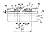
れたHEMTが、図1および2に示してあり、図1はHEMTの平面図であり、図2は断
面図である。HEMTは、基板10を含み、基板10は、例えば4Hポリタイプのシリコ
ンカーバイドなどの半絶縁性シリコンカーバイド(SiC)基板でよい。シリコンカーバ
イドポリタイプの他の候補は、3C、6Hおよび15Rポリタイプを含む。「半絶縁性」
という用語は、絶対的な意味ではなく、説明的なものとして使用される。本発明の特定の
諸実施形態では、シリコンカーバイドのバルク結晶が、室温で約1×10⁵Ω−cm以上
の抵抗率を有する。
造されており、そのような材料を製作する方法が、文献に記載されている(例えば、特許
文献5、特許文献6、特許文献7、特許文献8参照。)。同様に、III族窒化物のエピ
タキシアル成長技法についても開示されている(例えば、特許文献9、特許文献10、特
許文献11、特許文献12参照。)。
では、サファイア、窒化アルミニウム、窒化アルミニウムガリウム、窒化ガリウム、シリ
コン、GaAs、LGO、ZnO、LAO、InPなど、任意の適切な基板、あるいはI
II族窒化物材料の成長に対応することができる他の任意の材料または材料の組合せを利
用することができる。
えば、核形成層12が図2に示してある。核形成層が使用されるかどうかは、基板に使用
される材料による。核形成層は、基板と、デバイス内の次の層との間の格子不整合を低減
させるための適当な結晶構造の遷移をもたらす。例えば、さまざまな基板上に核形成層を
形成する方法が教示されている(例えば、特許文献13、特許文献14参照。)。シリコ
ンカーバイド基板上に核形成層を形成する方法が、開示されている(例えば、特許文献1
0、特許文献11、特許文献15参照。)。核形成層12は、約1000Åの厚さとすべ
きだが、他の厚さを使用することもできる。核形成層を、適切な材料がAlxGa1−x
N(0≦x≦1)である多くのさまざまな材料を使用して、また有機金属化学気相成長(
MOCVD)、ハイドライド気相エピタキシ(HVPE)、または分子線エピタキシ(M
BE)など、既知の半導体成長技法を使用して、基板上に堆積させることができる。
)を、文献に開示されているように含むこともできる(例えば、特許文献16、及び特許
文献17参照。)。
して、基板10上に堆積される。バッファ層14は、圧縮歪み(compressive strain)を
受けていてよい。さらに、バッファ層、および核形成層や遷移層などの他の層は、MOC
VD(有機金属化学気相成長)によって、あるいはMBE(分子線エピタキシ)またはH
VPE(ハイドライド気相エピタキシ)など、当業者には公知の他の半導体成長技法によ
って堆積させることができる。
ができ、好ましいバッファ層は、AlxGayIn1−x−yN(0≦x≦1、0≦y≦
1、x+y≦1)などのIII族窒化物材料で形成される。
りも大きな電子親和力を有するバッファ層14上に堆積される。バッファ層14と同様に
、バリア層16も、III族窒化物材料からなるドープ層または非ドープ層でよい。バリ
ア層はAlNでよく、またはいくつかの実施形態では、バリア層は、AlN層やAlGa
N層など、複数の層を含むことができる。適切なバリア層の例が、文献に開示されている
(例えば、特許文献3、特許文献4、特許文献18、特許文献19、特許文献20参照。
)。他の窒化物ベースHEMT構造が、文献に例示されている(例えば、特許文献1、特
許文献2参照。)。
250Åの厚さを有するAlGaN層とを含むことができる。バリア層は、十分に厚くあ
るべきであり、バッファ層14とバリア層16の間の境界面に分極効果によって十分なキ
ャリア濃度を誘起するために、十分に高いAlの組成およびドーピングを有すべきである
。こうすることにより、活性領域として知られる2次元電子ガス(2DEG)が、バッフ
ァ層とバリア層の間のヘテロ界面に形成される。
れる。オーム接点は、バリア層を通じて活性領域に抵抗率の低い接続をもたらすように、
(例えば、アニールによって)処理される。バリア層上のゲート接点22が、バリア層内
に深さDgまで広がってよい。図1に示すように、外部電気接続24を、ゲート22に設
けることができる。ゲートに適当なレベルでバイアスがかけられると、電流が、ソース電
極とドレイン電極の間に、バッファ層とバリア層の間のヘテロ界面に誘起された2DEG
を通って流れることができる。
ルの合金を含むがそれらに限定されない、さまざまな材料で形成することができる。ゲー
ト22も、金、ニッケル、白金、チタン、クロム、チタンとタングステンの合金、および
白金シリサイドを含むがそれらに限定されない、さまざまな材料で形成することができる
。ゲート22の長さLgはさまざまでよく、適切な長さは0.1から2μmの範囲内であ
るが、他のゲート長を使用することもできる。本発明による一実施形態では、好ましいゲ
ート長Lgは、約0.5μmである。
絶縁性スペーサ層28が、バリア層上でドレインとゲートの間に堆積される。任意選択で
、層26および28を初めに単一の層として形成し、それを後にエッチングにより貫通し
て、ゲート22を形成してもよい。スペーサ層26および28は、1層の誘電体層でも、
複数の誘電体層の組合せでもよい。SiN、SiO2、Si、Ge、MgOx、MgNx
、ZnO、SiNx、SiOx、ならびにそれらの合金および層を並べたものなどの、さ
まざまな誘電体材料を使用することができる。スペーサ層は、さまざまな厚さにすること
ができ、適切な厚さの範囲は、約0.05から2μmである。
はInの合金などの異なるIII族元素を有する、III族窒化物材料などのエピタキシ
アル材料とすることができ、適切なスペーサ層材料は、AlxGa1−xN(0.1≦x
≦1)である。バリア層16をエピタキシアル成長させた後、スペーサ層26および28
を、同じエピタキシアル成長法を使用して成長させることができる。
、ゲート22に電気的に接続される。スペーサ層28上でドレインとゲートの間にある第
2の導電性フィールドプレート32も、ゲートに電気的に接続される。フィールドプレー
ト30および32は、さまざまな導電性材料から形成することができ、適切な材料は、標
準的なメタライゼーション技法を使用して堆積される金属である。フィールドプレートを
備えるトランジスタおよびそうしたトランジスタを製作する方法が、文献に開示されてい
る(例えば、特許文献21、特許文献22、特許文献23参照。)。
第1のフィールドプレート30および第2のフィールドプレート32、ならびにゲート2
2上で、ソースとドレインの間に形成される。このスペーサ層は、第1および第2のスペ
ーサ層に関して上述したものと同様の材料で、また同様の処理によって形成することがで
きる。
ールドプレート、および第2のスペーサ層の上方で堆積され、ドレインに向かって延び、
ソースに電気的に接続される。第3のフィールドプレートは、ソースにさまざまな方法で
電気的に接続することができる。図1は、例えば、導電性バス38および40を介した接
続を示す。あるいは、外部バス42が接続を形成することもできる。他の接続構造を使用
することもできる。さまざまな数のバスを使用することができるが、使用されるバスが多
いほど、生じ得る望ましくない容量が大きくなる。生じる望ましくない容量の総量を最小
限に抑えるために、できるだけ少ないHEMTの活性領域を覆いながら、電流がソースか
らフィールドプレート内に効果的に分散することができるように、十分な本数のバスがあ
るべきである。
窒化シリコンなどの誘電体パッシベーション層(図示せず)によって覆うことができる。
誘電体パッシベーション層を形成する方法が、上述した特許文献および非特許文献に詳細
に記載されている。
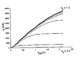
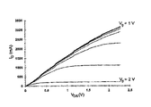
。図3および4に示すように、2Aの電流を伝えることができるデバイスにおいて、60
0Vを上回る阻止電圧が、5.0mΩ−cm2未満のオン抵抗とともに達成された。この
デバイスは、3Aの電流を伝えるときに5.3mΩ−cm2未満のオン抵抗も呈した。こ
のデバイスは、0.01cm2(1×1mm2)のデバイス面積、ならびに4Åの厚さの
AlN層および250Åの厚さのAlGaN層を含むバリア層を有する、SiC基板上の
GaN HEMTであった。第1のスペーサ層の厚さが0であり、第2のスペーサ層の厚
さが約1200Åであり、第3のスペーサ層の厚さが約1500Åであった。設計寸法は
、(図2を参照して)ゲート接点長Lg1.2μm、ゲートからドレインまでの距離Lg
d13.3μm、ドレインからソースまでの距離Lds16μm、第2のフィールドプレ
ート幅Lfd11.8μm、および第3のフィールドプレート幅Lfd24.5μmを含
んだ。
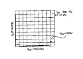
ドレイン電流ID対ドレイン−ソース電圧VDSのプロット図である。図4は、このデバ
イスが600Vの阻止電圧VBDを達成した様子を示す。
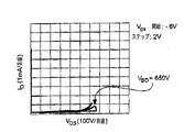
0Vを上回る阻止電圧が、6.6mΩ−cm2未満のオン抵抗とともに達成された。この
デバイスは、3Aの電流を伝えるときに7.0mΩ−cm2未満のオン抵抗も呈した。こ
のデバイスは、0.01cm2(1×1mm2)のデバイス面積、ならびに4Åの厚さの
AlN層および250Åの厚さのAlGaN層を含むバリア層を有する、SiC基板上の
GaN HEMTであった。第1のスペーサ層の厚さが0であり、第2のスペーサ層の厚
さが約1200Åであり、第3のスペーサ層の厚さが約1500Åであった。設計寸法は
、(図2を参照して)ゲート接点長Lg1.5μm、ゲートからドレインまでの距離Lg
d18.0μm、ドレインからソースまでの距離Lds21.5μm、第2のフィールド
プレート幅Lfd11.5μm、および第3のフィールドプレート幅Lfd24.5μm
を含んだ。
、ドレイン電流ID対ドレイン−ソース電圧VDSのプロット図である。図6は、このデ
バイスが900Vの阻止電圧VBDを達成した様子を示す。
実施形態では、本発明のデバイスを製作するための他の構造および/または技法を利用す
ることもできる。そうした構造および/または技法は、例えば、米国の本願の譲受人に譲
渡された、「Nitride Based Transistors on Semi-Insulating Silicon Carbide Substra
tes」(特許文献3)、「Aluminum Gallium Nitride/Gallium Nitride High Electron Mo
bility Transistors having a Gate Contact on a Gallium Nitride Based Cap Segment
and Methods of Fabricating Same」(特許文献24)、「Group III Nitride Based Hig
h Electron Mobility Transistor (HEMT) with Barrier/Spacer Layer」(特許文献19
)、「Nitride-based Transistors and Methods of Fabrication Thereof Using Non-Etc
hed Contact Recesses」(特許文献25)、「Nitride Heterojunction Transistors Hav
ing Charge-Transfer Induced Energy Barriers and Methods of Fabricating the Same
」(特許文献26)、「Methods of Fabricating Nitride-Based Transistors with a Ca
p Layer and a Recessed Gate」(特許文献27)、「Methods of Fabricating Nitride-
Based Transistors having Regrown Ohmic Contact Regions and Nitride-Based Transis
tors having Regrown Ohmic Contact Regions」(特許文献28)、「Semiconductor Dev
ices having a Hybrid Channel Layer, Current Aperture Transistors and Methods of
Fabricating Same」(特許文献29)、「Insulating Gate AlGaN/GaN HEMT」(特許文献
20)、および「Cap Layers and/or Passivation Layers for Nitride-Based Transisto
rs, Transistor Structures and Methods of Fabricating Same」(特許文献30)に記
載されているものを含むことができる。
発明を限定するものではないことに留意されたい。図面では、層や領域などの構成要素の
厚さが、見やすくするために誇張される場合がある。同じ数字は、明細書全体を通じて同
じ要素を表す。「および/または」という語は、列挙された関連する諸項目の1つまたは
複数のあらゆる組合せを含む。
合を除き、複数形も含むものとする。「備える(comprises、comprisi
ng)」という語は、本明細書中で使用される場合、述べられた特徴、整数、ステップ、
動作、要素および/または構成要素の存在を特定するが、1つあるいは複数の他の特徴、
整数、ステップ、動作、要素、構成要素および/またはそれらの群の、存在または追加を
妨げない。
延びているという場合、その要素は、直接他の要素上にあっても、他の要素上に延びても
よく、または介在する要素が存在してもよい。それとは対照的に、要素が、別の要素の「
直接上に」ある、または別の要素の「直接上に」延びているという場合、介在する要素は
存在しない。さらに、要素が別の要素に「接続されている」または「結合されている」と
いう場合、その要素は、直接他の要素に接続されても、結合されてもよく、または介在す
る要素が存在してもよい。それとは対照的に、要素が別の要素に「直接接続されている」
または「直接結合されている」という場合、介在する要素は存在しない。
、第1、第2などの語が使用されることがあるが、それらの要素は、こうした語によって
限定されない。そうではなく、こうした語は、ある要素、構成要素、領域、層、または部
分を、別のものと区別するために使用される。したがって、例えば、第1の要素、構成要
素、領域、層または部分は、本発明の教示から逸脱することなく、第2の要素、構成要素
、領域、層または部分と呼ぶことができる。
面中に示した、ある要素の別の要素との関係を説明するために使用されることがある。そ
のような相対語は、図面内に示された向きに加えて、デバイスのさまざまな向きを含むも
のである。例えば、図面内のデバイスが裏返しにされる場合、他の要素の「低い方の」側
にあると説明された要素は、他の要素の「高い方の」側に向けられることになる。したが
って、「低い方の」という例示的な語は、図面の特定の向きに応じて、「低い方の」と「
高い方の」のどちらも含むことができる。同様に、「下の(below、beneath
)」という例示的な語は、上の向きと下の向きのどちらも含むことができる。さらに、「
外側の」という語は、基板から最も遠く離れた表面および/または層を指すのに使用する
ことができる。
図および/または他の図を参照して説明される。したがって、例えば製造技法および/ま
たは公差(tolerance)の結果として、図の形状との違いが予想される。したがって、本
発明の諸実施形態は、図示の特定の形状に限定されると解釈すべきではなく、例えば製造
から生じるずれを含むべきである。例えば、長方形として示されるエッチングされた領域
は、実際には一般に、テーパ状の特徴、丸い特徴または曲線状の特徴を有する。別の特徴
に「隣接して」配設される構造または特徴という言及は、隣接する特徴とオーバラップす
る、またはその下にある部分を含むことがある。
る用語は、本発明に関係する当業者によって一般に理解される意味を有する。さらに、一
般に使用される辞書で定義されるような用語は、関連技術の文脈におけるその意味と一致
する意味を有すると解釈すべきであり、そのような用語は、本明細書において明示的にそ
のように定義されない限り、理想化されたまたは過度に形式的な意味として解釈すべきで
ない。
態および追加の実施形態を含む他のバージョンが、当業者には疑問の余地なく明らかとな
るであろう。例えば、フィールドプレートの配置を、多くのさまざまなデバイスで使用す
ることができる。フィールドプレートは、さまざまな形状を有することもでき、ソース接
点にさまざまな方法で接続することができる。さらに、本発明は、パワースイッチング用
途に特に有用であるが、例えばスイッチモード電源および高電圧モータ駆動装置用の直流
−直流変換器などの他の用途にも、そうしたシステムでの効率増大およびサイズ低減を助
けるために使用することができる。したがって、本発明の趣旨および範囲は、本明細書に
記載の本発明の諸実施形態に限定すべきではない。そうではなく、それらの実施形態は、
本開示を網羅的で完全なものにするために、また本発明の範囲を当業者に十分に伝えるた
めに、提供されるものである。
品または接続を逆にする、あるいは交換することができ、本発明のいくつかの特徴を、他
の特徴とは関わりなく利用することができる。したがって、例示的な諸実施形態は、包括
的ではなく例示的なものと見なすべきであるとともに、添付の特許請求の範囲が、本発明
の全範囲を定義するものとする。
Claims (12)
- 多重フィールドプレートトランジスタであって、
活性領域と、
前記活性領域と電気的に接触しているソース電極と、
前記活性領域と電気的に接触しているドレイン電極と、
前記活性領域と電気的に接触している、前記ソースと前記ドレインの間のゲートと、
前記活性領域の上方で前記ソースと前記ゲートの間に配設された第1の絶縁性スペーサ
層と、
前記活性領域の上方で前記ドレインと前記ゲートの間に配設された第2の絶縁性スペー
サ層と、
前記ソースと前記ゲートの間にある前記第1のスペーサ層上に配設され、前記ゲートに
電気的に接続され、前記ソースに向かって延びる第1の導電性フィールドプレートと、
前記ドレインと前記ゲートの間にある前記第2のスペーサ層上に配設され、前記ゲート
に電気的に接続され、前記ドレインに向かって延びる第2の導電性フィールドプレートと
、
前記第1のスペーサ層、前記第2のスペーサ層、前記第1のフィールドプレート、前記
ゲート、および前記第2のフィールドプレート上で、前記ソースと前記ドレインの間に配
設された第3の絶縁性スペーサ層と、
前記第3のスペーサ層上に、前記ゲート、前記第2のフィールドプレート、および前記
第2のスペーサ層の上方で配設され、前記ソースに電気的に接続され、前記ドレインに向
かって延びる第3の導電性フィールドプレートと
を備えたことを特徴とする多重フィールドプレートトランジスタ。 - 少なくとも600ボルトの阻止電圧を呈するとともに、5.0mΩ−cm2以下のオン
抵抗で少なくとも2アンペアの電流に対応するように構成されたことを特徴とする請求項
1に記載のトランジスタ。 - 少なくとも600ボルトの阻止電圧を呈するとともに、5.3mΩ−cm2以下のオン
抵抗で少なくとも3アンペアの電流に対応するように構成されたことを特徴とする請求項
1に記載のトランジスタ。 - 少なくとも900ボルトの阻止電圧を呈するとともに、6.6mΩ−cm2以下のオン
抵抗で少なくとも2アンペアの電流に対応するように構成されたことを特徴とする請求項
1に記載のトランジスタ。 - 少なくとも900ボルトの阻止電圧を呈するとともに、7.0mΩ−cm2以下のオン
抵抗で少なくとも3アンペアの電流に対応するように構成されたことを特徴とする請求項
1に記載のトランジスタ。 - 前記第1のスペーサ層および前記第2のスペーサ層が、前記活性領域の表面上に配設さ
れた単一層の部分を備えたことを特徴とする請求項1に記載のトランジスタ。 - 高電子移動度トランジスタを備えたことを特徴とする請求項1に記載のトランジスタ。
- 基板と、
前記基板上に配設されたバッファ層と、
前記バッファ層上に配設されたバリア層と
をさらに備え、
前記活性領域が、前記バッファ層と前記バリア層との間のヘテロ界面に誘起される2次
元電子ガスによって画定されたことを特徴とする請求項7に記載のトランジスタ。 - 前記ゲートが、前記バリア層内に部分的に凹んだことを特徴とする請求項8に記載のト
ランジスタ。 - 前記基板が、半絶縁性SiC基板を備えたことを特徴とする請求項8に記載のトランジ
スタ。 - 前記第1のスペーサ層は、第1のSiNスペーサ層を備え、前記第2のスペーサ層は、
第2のSiNスペーサ層を備え、前記第3のスペーサ層は、第3のSiNスペーサ層を備
えたことを特徴とする請求項8に記載のトランジスタ。 - 前記第1のフィールドプレートは、第1の金属フィールドプレートを備え、前記第2の
フィールドプレートは、第2の金属フィールドプレートを備え、前記第3のフィールドプ
レートは、第3の金属フィールドプレートを備えたことを特徴とする請求項8に記載のト
ランジスタ。
Applications Claiming Priority (2)
| Application Number | Priority Date | Filing Date | Title |
|---|---|---|---|
| US11/603,427 | 2006-11-21 | ||
| US11/603,427 US7692263B2 (en) | 2006-11-21 | 2006-11-21 | High voltage GaN transistors |
Related Parent Applications (1)
| Application Number | Title | Priority Date | Filing Date |
|---|---|---|---|
| JP2007245497A Division JP5546099B2 (ja) | 2006-11-21 | 2007-09-21 | 高電圧GaNトランジスタ |
Publications (2)
| Publication Number | Publication Date |
|---|---|
| JP2012178593A true JP2012178593A (ja) | 2012-09-13 |
| JP5705161B2 JP5705161B2 (ja) | 2015-04-22 |
Family
ID=39416066
Family Applications (4)
| Application Number | Title | Priority Date | Filing Date |
|---|---|---|---|
| JP2007245497A Active JP5546099B2 (ja) | 2006-11-21 | 2007-09-21 | 高電圧GaNトランジスタ |
| JP2012106266A Active JP5705161B2 (ja) | 2006-11-21 | 2012-05-07 | トランジスタ装置 |
| JP2012106264A Active JP5738798B2 (ja) | 2006-11-21 | 2012-05-07 | トランジスタ装置 |
| JP2012106265A Pending JP2012147034A (ja) | 2006-11-21 | 2012-05-07 | 多重フィールドプレートトランジスタ |
Family Applications Before (1)
| Application Number | Title | Priority Date | Filing Date |
|---|---|---|---|
| JP2007245497A Active JP5546099B2 (ja) | 2006-11-21 | 2007-09-21 | 高電圧GaNトランジスタ |
Family Applications After (2)
| Application Number | Title | Priority Date | Filing Date |
|---|---|---|---|
| JP2012106264A Active JP5738798B2 (ja) | 2006-11-21 | 2012-05-07 | トランジスタ装置 |
| JP2012106265A Pending JP2012147034A (ja) | 2006-11-21 | 2012-05-07 | 多重フィールドプレートトランジスタ |
Country Status (3)
| Country | Link |
|---|---|
| US (5) | US7692263B2 (ja) |
| EP (2) | EP2485262B1 (ja) |
| JP (4) | JP5546099B2 (ja) |
Families Citing this family (116)
| Publication number | Priority date | Publication date | Assignee | Title |
|---|---|---|---|---|
| EP2267784B1 (en) * | 2001-07-24 | 2020-04-29 | Cree, Inc. | INSULATING GATE AlGaN/GaN HEMT |
| WO2005024909A2 (en) * | 2003-09-09 | 2005-03-17 | The Regents Of The University Of California | Fabrication of single or multiple gate field plates |
| US9773877B2 (en) | 2004-05-13 | 2017-09-26 | Cree, Inc. | Wide bandgap field effect transistors with source connected field plates |
| US11791385B2 (en) | 2005-03-11 | 2023-10-17 | Wolfspeed, Inc. | Wide bandgap transistors with gate-source field plates |
| US7972915B2 (en) * | 2005-11-29 | 2011-07-05 | The Hong Kong University Of Science And Technology | Monolithic integration of enhancement- and depletion-mode AlGaN/GaN HFETs |
| US7932539B2 (en) * | 2005-11-29 | 2011-04-26 | The Hong Kong University Of Science And Technology | Enhancement-mode III-N devices, circuits, and methods |
| US8044432B2 (en) * | 2005-11-29 | 2011-10-25 | The Hong Kong University Of Science And Technology | Low density drain HEMTs |
| US7692263B2 (en) | 2006-11-21 | 2010-04-06 | Cree, Inc. | High voltage GaN transistors |
| US7838904B2 (en) * | 2007-01-31 | 2010-11-23 | Panasonic Corporation | Nitride based semiconductor device with concave gate region |
| US8212290B2 (en) | 2007-03-23 | 2012-07-03 | Cree, Inc. | High temperature performance capable gallium nitride transistor |
| CN101359686B (zh) * | 2007-08-03 | 2013-01-02 | 香港科技大学 | 可靠的常关型ⅲ-氮化物有源器件结构及相关方法和系统 |
| JP5217301B2 (ja) * | 2007-08-28 | 2013-06-19 | 富士通株式会社 | 化合物半導体装置とその製造方法 |
| US7915643B2 (en) | 2007-09-17 | 2011-03-29 | Transphorm Inc. | Enhancement mode gallium nitride power devices |
| US20090072269A1 (en) * | 2007-09-17 | 2009-03-19 | Chang Soo Suh | Gallium nitride diodes and integrated components |
| US8076699B2 (en) * | 2008-04-02 | 2011-12-13 | The Hong Kong Univ. Of Science And Technology | Integrated HEMT and lateral field-effect rectifier combinations, methods, and systems |
| US8519438B2 (en) * | 2008-04-23 | 2013-08-27 | Transphorm Inc. | Enhancement mode III-N HEMTs |
| US8289065B2 (en) | 2008-09-23 | 2012-10-16 | Transphorm Inc. | Inductive load power switching circuits |
| US20100084687A1 (en) * | 2008-10-03 | 2010-04-08 | The Hong Kong University Of Science And Technology | Aluminum gallium nitride/gallium nitride high electron mobility transistors |
| US7898004B2 (en) | 2008-12-10 | 2011-03-01 | Transphorm Inc. | Semiconductor heterostructure diodes |
| EP2380198A1 (de) * | 2009-01-07 | 2011-10-26 | Microgan Gmbh | Selbstsperrender schalter |
| TWI514568B (zh) | 2009-04-08 | 2015-12-21 | Efficient Power Conversion Corp | 增強模式氮化鎵高電子遷移率電晶體元件及其製造方法 |
| US8823012B2 (en) * | 2009-04-08 | 2014-09-02 | Efficient Power Conversion Corporation | Enhancement mode GaN HEMT device with gate spacer and method for fabricating the same |
| US9502973B2 (en) | 2009-04-08 | 2016-11-22 | Infineon Technologies Americas Corp. | Buck converter with III-nitride switch for substantially increased input-to-output voltage ratio |
| US8008977B2 (en) * | 2009-04-14 | 2011-08-30 | Triquint Semiconductor, Inc. | Field-plated transistor including feedback resistor |
| US8754496B2 (en) * | 2009-04-14 | 2014-06-17 | Triquint Semiconductor, Inc. | Field effect transistor having a plurality of field plates |
| US8742459B2 (en) | 2009-05-14 | 2014-06-03 | Transphorm Inc. | High voltage III-nitride semiconductor devices |
| US8390000B2 (en) | 2009-08-28 | 2013-03-05 | Transphorm Inc. | Semiconductor devices with field plates |
| US9136364B2 (en) | 2009-09-16 | 2015-09-15 | Power Integrations, Inc. | Field effect transistor with access region recharge |
| US8389977B2 (en) | 2009-12-10 | 2013-03-05 | Transphorm Inc. | Reverse side engineered III-nitride devices |
| WO2011100304A1 (en) | 2010-02-09 | 2011-08-18 | Massachusetts Institute Of Technology | Dual-gate normally-off nitride transistors |
| US20110241020A1 (en) * | 2010-03-31 | 2011-10-06 | Triquint Semiconductor, Inc. | High electron mobility transistor with recessed barrier layer |
| JP2011249728A (ja) * | 2010-05-31 | 2011-12-08 | Toshiba Corp | 半導体装置および半導体装置の製造方法 |
| KR101680767B1 (ko) * | 2010-10-06 | 2016-11-30 | 삼성전자주식회사 | 불순물 주입을 이용한 고출력 고 전자 이동도 트랜지스터 제조방법 |
| US8742460B2 (en) | 2010-12-15 | 2014-06-03 | Transphorm Inc. | Transistors with isolation regions |
| US8643062B2 (en) | 2011-02-02 | 2014-02-04 | Transphorm Inc. | III-N device structures and methods |
| JP5776217B2 (ja) * | 2011-02-24 | 2015-09-09 | 富士通株式会社 | 化合物半導体装置 |
| US8772842B2 (en) | 2011-03-04 | 2014-07-08 | Transphorm, Inc. | Semiconductor diodes with low reverse bias currents |
| US8716141B2 (en) | 2011-03-04 | 2014-05-06 | Transphorm Inc. | Electrode configurations for semiconductor devices |
| US9024357B2 (en) | 2011-04-15 | 2015-05-05 | Stmicroelectronics S.R.L. | Method for manufacturing a HEMT transistor and corresponding HEMT transistor |
| KR20120120826A (ko) | 2011-04-25 | 2012-11-02 | 삼성전기주식회사 | 질화물 반도체 소자 및 그 제조방법 |
| US8901604B2 (en) | 2011-09-06 | 2014-12-02 | Transphorm Inc. | Semiconductor devices with guard rings |
| US9257547B2 (en) | 2011-09-13 | 2016-02-09 | Transphorm Inc. | III-N device structures having a non-insulating substrate |
| US8772833B2 (en) | 2011-09-21 | 2014-07-08 | Electronics And Telecommunications Research Institute | Power semiconductor device and fabrication method thereof |
| US8598937B2 (en) | 2011-10-07 | 2013-12-03 | Transphorm Inc. | High power semiconductor electronic components with increased reliability |
| US8530978B1 (en) * | 2011-12-06 | 2013-09-10 | Hrl Laboratories, Llc | High current high voltage GaN field effect transistors and method of fabricating same |
| KR101869045B1 (ko) * | 2012-01-11 | 2018-06-19 | 삼성전자 주식회사 | 고전자이동도 트랜지스터 및 그 제조방법 |
| US9165766B2 (en) | 2012-02-03 | 2015-10-20 | Transphorm Inc. | Buffer layer structures suited for III-nitride devices with foreign substrates |
| US9093366B2 (en) | 2012-04-09 | 2015-07-28 | Transphorm Inc. | N-polar III-nitride transistors |
| EP2662884B1 (en) | 2012-05-09 | 2015-04-01 | Nxp B.V. | Group 13 nitride semiconductor device and method of its manufacture |
| US9443941B2 (en) * | 2012-06-04 | 2016-09-13 | Infineon Technologies Austria Ag | Compound semiconductor transistor with self aligned gate |
| US9184275B2 (en) | 2012-06-27 | 2015-11-10 | Transphorm Inc. | Semiconductor devices with integrated hole collectors |
| US10192981B2 (en) | 2012-06-29 | 2019-01-29 | Power Integrations, Inc. | Switching device with charge distribution structure |
| US9245879B2 (en) | 2012-06-29 | 2016-01-26 | Power Integrations, Inc. | Static discharge system |
| US8815647B2 (en) * | 2012-09-04 | 2014-08-26 | Infineon Technologies Ag | Chip package and a method for manufacturing a chip package |
| CN103123934B (zh) * | 2013-02-07 | 2015-08-12 | 中国科学院半导体研究所 | 具势垒层的氮化镓基高电子迁移率晶体管结构及制作方法 |
| US9171730B2 (en) | 2013-02-15 | 2015-10-27 | Transphorm Inc. | Electrodes for semiconductor devices and methods of forming the same |
| US9087718B2 (en) | 2013-03-13 | 2015-07-21 | Transphorm Inc. | Enhancement-mode III-nitride devices |
| US9245992B2 (en) | 2013-03-15 | 2016-01-26 | Transphorm Inc. | Carbon doping semiconductor devices |
| US9847411B2 (en) * | 2013-06-09 | 2017-12-19 | Cree, Inc. | Recessed field plate transistor structures |
| US9755059B2 (en) | 2013-06-09 | 2017-09-05 | Cree, Inc. | Cascode structures with GaN cap layers |
| US9679981B2 (en) * | 2013-06-09 | 2017-06-13 | Cree, Inc. | Cascode structures for GaN HEMTs |
| DE102013211360A1 (de) * | 2013-06-18 | 2014-12-18 | Robert Bosch Gmbh | Halbleiter-Leistungsschalter und Verfahren zur Herstellung eines Halbleiter-Leistungsschalters |
| WO2015009514A1 (en) | 2013-07-19 | 2015-01-22 | Transphorm Inc. | Iii-nitride transistor including a p-type depleting layer |
| SG10201804591WA (en) | 2013-10-18 | 2018-07-30 | Agency Science Tech & Res | Semiconductor device fabrication |
| US10593767B2 (en) * | 2013-12-23 | 2020-03-17 | Chun Wai NG | Field plate structure for power semiconductor device and manufacturing method thereof |
| US9123791B2 (en) | 2014-01-09 | 2015-09-01 | Infineon Technologies Austria Ag | Semiconductor device and method |
| US9425301B2 (en) | 2014-04-30 | 2016-08-23 | Taiwan Semiconductor Manufacturing Co., Ltd. | Sidewall passivation for HEMT devices |
| US10276712B2 (en) | 2014-05-29 | 2019-04-30 | Hrl Laboratories, Llc | III-nitride field-effect transistor with dual gates |
| US9318593B2 (en) | 2014-07-21 | 2016-04-19 | Transphorm Inc. | Forming enhancement mode III-nitride devices |
| US9620598B2 (en) * | 2014-08-05 | 2017-04-11 | Semiconductor Components Industries, Llc | Electronic device including a channel layer including gallium nitride |
| US9640623B2 (en) * | 2014-10-17 | 2017-05-02 | Cree, Inc. | Semiconductor device with improved field plate |
| CN104409493B (zh) * | 2014-11-18 | 2017-03-29 | 西安电子科技大学 | 基于t形栅‑漏复合场板的异质结器件及其制作方法 |
| US9536967B2 (en) | 2014-12-16 | 2017-01-03 | Transphorm Inc. | Recessed ohmic contacts in a III-N device |
| US9536966B2 (en) | 2014-12-16 | 2017-01-03 | Transphorm Inc. | Gate structures for III-N devices |
| JP6496149B2 (ja) | 2015-01-22 | 2019-04-03 | ローム株式会社 | 半導体装置および半導体装置の製造方法 |
| US9543402B1 (en) * | 2015-08-04 | 2017-01-10 | Power Integrations, Inc. | Integrated high performance lateral schottky diode |
| US9812532B1 (en) | 2015-08-28 | 2017-11-07 | Hrl Laboratories, Llc | III-nitride P-channel transistor |
| EP3378097A4 (en) | 2015-11-19 | 2019-09-11 | HRL Laboratories, LLC | NITRIDE-III FIELD EFFECT TRANSISTOR WITH DOUBLE TRIGGER |
| US11322599B2 (en) | 2016-01-15 | 2022-05-03 | Transphorm Technology, Inc. | Enhancement mode III-nitride devices having an Al1-xSixO gate insulator |
| CN107230713A (zh) * | 2016-03-25 | 2017-10-03 | 北京大学 | 半导体器件及制造方法 |
| US20170301780A1 (en) * | 2016-04-15 | 2017-10-19 | Macom Technology Solutions Holdings, Inc. | High-voltage gan high electron mobility transistors with reduced leakage current |
| US10985284B2 (en) | 2016-04-15 | 2021-04-20 | Macom Technology Solutions Holdings, Inc. | High-voltage lateral GaN-on-silicon schottky diode with reduced junction leakage current |
| US10217827B2 (en) * | 2016-05-11 | 2019-02-26 | Rfhic Corporation | High electron mobility transistor (HEMT) |
| TWI813243B (zh) | 2016-05-31 | 2023-08-21 | 美商創世舫科技有限公司 | 包含漸變空乏層的三族氮化物裝置 |
| US10892356B2 (en) | 2016-06-24 | 2021-01-12 | Cree, Inc. | Group III-nitride high-electron mobility transistors with buried p-type layers and process for making the same |
| US10192980B2 (en) | 2016-06-24 | 2019-01-29 | Cree, Inc. | Gallium nitride high-electron mobility transistors with deep implanted p-type layers in silicon carbide substrates for power switching and radio frequency applications and process for making the same |
| US11430882B2 (en) | 2016-06-24 | 2022-08-30 | Wolfspeed, Inc. | Gallium nitride high-electron mobility transistors with p-type layers and process for making the same |
| US10840334B2 (en) | 2016-06-24 | 2020-11-17 | Cree, Inc. | Gallium nitride high-electron mobility transistors with deep implanted p-type layers in silicon carbide substrates for power switching and radio frequency applications and process for making the same |
| DE102016123934A1 (de) | 2016-12-09 | 2018-06-14 | United Monolithic Semiconductors Gmbh | Verfahren zur Herstellung eines Transistors |
| DE102016123931A1 (de) | 2016-12-09 | 2018-06-14 | United Monolithic Semiconductors Gmbh | Transistor |
| US9923069B1 (en) * | 2017-02-28 | 2018-03-20 | Panasonic Intellectual Property Management Co., Ltd. | Nitride semiconductor device |
| TWI736600B (zh) | 2017-03-31 | 2021-08-21 | 聯穎光電股份有限公司 | 高電子遷移率電晶體 |
| TWI722166B (zh) * | 2017-04-10 | 2021-03-21 | 聯穎光電股份有限公司 | 高電子遷移率電晶體 |
| US9998109B1 (en) * | 2017-05-15 | 2018-06-12 | Cree, Inc. | Power module with improved reliability |
| JP2017208556A (ja) * | 2017-06-27 | 2017-11-24 | 株式会社東芝 | 半導体装置 |
| US20190097001A1 (en) | 2017-09-25 | 2019-03-28 | Raytheon Company | Electrode structure for field effect transistor |
| US10418474B2 (en) | 2017-10-17 | 2019-09-17 | Mitsubishi Electric Research Laboratories, Inc. | High electron mobility transistor with varying semiconductor layer |
| US10276704B1 (en) | 2017-10-17 | 2019-04-30 | Mitsubishi Electric Research Laboratiories, Inc. | High electron mobility transistor with negative capacitor gate |
| US10720497B2 (en) | 2017-10-24 | 2020-07-21 | Raytheon Company | Transistor having low capacitance field plate structure |
| US10700188B2 (en) | 2017-11-02 | 2020-06-30 | Rohm Co., Ltd. | Group III nitride semiconductor device with first and second conductive layers |
| US10431695B2 (en) | 2017-12-20 | 2019-10-01 | Micron Technology, Inc. | Transistors comprising at lease one of GaP, GaN, and GaAs |
| US10825816B2 (en) | 2017-12-28 | 2020-11-03 | Micron Technology, Inc. | Recessed access devices and DRAM constructions |
| US10950598B2 (en) | 2018-01-19 | 2021-03-16 | Macom Technology Solutions Holdings, Inc. | Heterolithic microwave integrated circuits including gallium-nitride devices formed on highly doped semiconductor |
| US11056483B2 (en) | 2018-01-19 | 2021-07-06 | Macom Technology Solutions Holdings, Inc. | Heterolithic microwave integrated circuits including gallium-nitride devices on intrinsic semiconductor |
| US11233047B2 (en) | 2018-01-19 | 2022-01-25 | Macom Technology Solutions Holdings, Inc. | Heterolithic microwave integrated circuits including gallium-nitride devices on highly doped regions of intrinsic silicon |
| US10734527B2 (en) | 2018-02-06 | 2020-08-04 | Micron Technology, Inc. | Transistors comprising a pair of source/drain regions having a channel there-between |
| JP7108364B2 (ja) | 2018-09-04 | 2022-07-28 | キヤノン電子管デバイス株式会社 | 放射線検出器、放射線検出器の製造方法および装置、並びにシンチレータパネル、シンチレータパネルの製造方法および装置 |
| US11276765B2 (en) * | 2019-06-25 | 2022-03-15 | Wolfspeed, Inc. | Composite-channel high electron mobility transistor |
| CN112531025B (zh) | 2019-09-17 | 2024-01-30 | 联华电子股份有限公司 | 高电子迁移率晶体管 |
| CN117976705A (zh) | 2019-10-30 | 2024-05-03 | 联华电子股份有限公司 | 高电子迁移率晶体管及其制作方法 |
| TWI729600B (zh) * | 2019-12-03 | 2021-06-01 | 財團法人亞洲大學 | 高電壓氮化鎵電晶體及其製造方法 |
| US11695068B2 (en) | 2020-03-09 | 2023-07-04 | Insyt, Inc. | Greyscale lithography for double-slanted gate connected field plate |
| WO2021195506A1 (en) | 2020-03-26 | 2021-09-30 | Macom Technology Solutions Holdings, Inc. | Microwave integrated circuits including gallium-nitride devices on silicon |
| US11855198B2 (en) * | 2020-04-09 | 2023-12-26 | Qualcomm Incorporated | Multi-gate high electron mobility transistors (HEMTs) employing tuned recess depth gates for improved device linearity |
| CN116601777A (zh) * | 2021-01-29 | 2023-08-15 | 华为技术有限公司 | 晶体管、电子器件及终端设备 |
| US11929428B2 (en) | 2021-05-17 | 2024-03-12 | Wolfspeed, Inc. | Circuits and group III-nitride high-electron mobility transistors with buried p-type layers improving overload recovery and process for implementing the same |
Citations (6)
| Publication number | Priority date | Publication date | Assignee | Title |
|---|---|---|---|---|
| JPS63188964U (ja) * | 1987-05-28 | 1988-12-05 | ||
| JPH0366136A (ja) * | 1989-08-04 | 1991-03-20 | Fujitsu Ltd | 半導体装置 |
| JP2001251869A (ja) * | 2000-03-01 | 2001-09-14 | Osaka Gas Co Ltd | 直交変換回路、電力変換装置、及び、発電システム |
| JP2003100778A (ja) * | 2001-09-26 | 2003-04-04 | Toshiba Corp | 半導体装置 |
| WO2005114743A2 (en) * | 2004-05-11 | 2005-12-01 | Cree, Inc. | Wide bandgap transistors with multiple field plates |
| WO2006098801A1 (en) * | 2005-03-11 | 2006-09-21 | Cree, Inc. | Wide bandgap transistors with gate-source field plates |
Family Cites Families (158)
| Publication number | Priority date | Publication date | Assignee | Title |
|---|---|---|---|---|
| BE792908A (fr) | 1971-12-20 | 1973-04-16 | Western Electric Co | Procede de fabrication de dispositifs semi-conducteurs |
| JPS4886473U (ja) | 1972-01-19 | 1973-10-19 | ||
| JPS51129173A (en) | 1974-02-01 | 1976-11-10 | Chisso Corp | Semi conductor with high voltage proof schottky electrode and it's man uacturing method. |
| JPS5539636Y2 (ja) | 1974-07-15 | 1980-09-17 | ||
| JPS51129173U (ja) | 1975-03-29 | 1976-10-19 | ||
| JPS5618429Y2 (ja) | 1976-10-25 | 1981-04-30 | ||
| JPS5360567A (en) | 1976-11-11 | 1978-05-31 | Mitsubishi Electric Corp | Electrode formation method of semiconductor device |
| JPS5539636A (en) | 1978-09-13 | 1980-03-19 | Nec Corp | Composite semiconductor |
| US4947232A (en) * | 1980-03-22 | 1990-08-07 | Sharp Kabushiki Kaisha | High voltage MOS transistor |
| NL8103218A (nl) | 1981-07-06 | 1983-02-01 | Philips Nv | Veldeffekttransistor met geisoleerde stuurelektrode. |
| US4551905A (en) * | 1982-12-09 | 1985-11-12 | Cornell Research Foundation, Inc. | Fabrication of metal lines for semiconductor devices |
| DE3323347A1 (de) | 1983-06-29 | 1985-01-10 | Neff Gewindespindeln GmbH, 7035 Waldenbuch | Kugelumlauf-schraubgetriebe |
| JPS60136881U (ja) | 1984-02-20 | 1985-09-11 | 三菱重工業株式会社 | 多点同時点溶接装置 |
| JPS62136881A (ja) | 1985-12-11 | 1987-06-19 | Fujitsu Ltd | 半導体装置 |
| JPS63139718A (ja) | 1986-12-01 | 1988-06-11 | Canon Inc | 樹脂成形品およびその成形方法 |
| US4689869A (en) | 1986-04-07 | 1987-09-01 | International Business Machines Corporation | Fabrication of insulated gate gallium arsenide FET with self-aligned source/drain and submicron channel length |
| JPS63188964A (ja) | 1987-01-31 | 1988-08-04 | Dainippon Printing Co Ltd | 集積回路パツケ−ジ |
| US4866005A (en) | 1987-10-26 | 1989-09-12 | North Carolina State University | Sublimation of silicon carbide to produce large, device quality single crystals of silicon carbide |
| US5196359A (en) * | 1988-06-30 | 1993-03-23 | Texas Instruments Incorporated | Method of forming heterostructure field effect transistor |
| DE3823347A1 (de) | 1988-07-09 | 1990-01-11 | Semikron Elektronik Gmbh | Leistungs-halbleiterelement |
| DE69031813T2 (de) | 1989-04-04 | 1998-04-09 | Siemens Ag | HEMT-Struktur |
| US5252843A (en) * | 1989-09-01 | 1993-10-12 | Fujitsu Limited | Semiconductor device having overlapping conductor layers |
| US4946547A (en) | 1989-10-13 | 1990-08-07 | Cree Research, Inc. | Method of preparing silicon carbide surfaces for crystal growth |
| US5210051A (en) | 1990-03-27 | 1993-05-11 | Cree Research, Inc. | High efficiency light emitting diodes from bipolar gallium nitride |
| US5200022A (en) | 1990-10-03 | 1993-04-06 | Cree Research, Inc. | Method of improving mechanically prepared substrate surfaces of alpha silicon carbide for deposition of beta silicon carbide thereon and resulting product |
| US5290393A (en) | 1991-01-31 | 1994-03-01 | Nichia Kagaku Kogyo K.K. | Crystal growth method for gallium nitride-based compound semiconductor |
| EP0576566B1 (en) | 1991-03-18 | 1999-05-26 | Trustees Of Boston University | A method for the preparation and doping of highly insulating monocrystalline gallium nitride thin films |
| US5192987A (en) * | 1991-05-17 | 1993-03-09 | Apa Optics, Inc. | High electron mobility transistor with GaN/Alx Ga1-x N heterojunctions |
| JPH0521793A (ja) | 1991-07-09 | 1993-01-29 | Mitsubishi Electric Corp | 半導体装置及びその製造方法 |
| JP2702338B2 (ja) * | 1991-10-14 | 1998-01-21 | 三菱電機株式会社 | 半導体装置、及びその製造方法 |
| JP3019885B2 (ja) | 1991-11-25 | 2000-03-13 | カシオ計算機株式会社 | 電界効果型薄膜トランジスタの製造方法 |
| US5236395A (en) | 1991-11-27 | 1993-08-17 | Reliance Electric Industrial Company | Maintenance friendly variable speed drive and methods |
| JPH05326890A (ja) | 1992-05-07 | 1993-12-10 | Nec Corp | 出力バッファ回路 |
| EP0569745A1 (de) * | 1992-05-14 | 1993-11-18 | Siemens Aktiengesellschaft | Verfahren zur Herstellung eines Feldeffekttransistoren mit asymmetrischer Gate-Struktur |
| JPH06124965A (ja) | 1992-10-09 | 1994-05-06 | Sumitomo Electric Ind Ltd | 電界効果トランジスタ |
| JPH06224225A (ja) * | 1993-01-27 | 1994-08-12 | Fujitsu Ltd | 電界効果半導体装置 |
| US5393993A (en) | 1993-12-13 | 1995-02-28 | Cree Research, Inc. | Buffer structure between silicon carbide and gallium nitride and resulting semiconductor devices |
| JPH07283140A (ja) | 1994-04-05 | 1995-10-27 | Nippon Telegr & Teleph Corp <Ntt> | 活性原子の供給制御方法 |
| JPH07326737A (ja) | 1994-05-31 | 1995-12-12 | Nippon Steel Corp | インピーダンス線路、フィルタ素子、遅延素子および半導体装置 |
| US5592501A (en) | 1994-09-20 | 1997-01-07 | Cree Research, Inc. | Low-strain laser structures with group III nitride active layers |
| US5523589A (en) | 1994-09-20 | 1996-06-04 | Cree Research, Inc. | Vertical geometry light emitting diode with group III nitride active layer and extended lifetime |
| GB2296373B (en) | 1994-12-14 | 1997-09-10 | Toshiba Cambridge Res Center | Semiconductor device |
| US5828084A (en) | 1995-03-27 | 1998-10-27 | Sony Corporation | High performance poly-SiGe thin film transistor |
| US5670798A (en) * | 1995-03-29 | 1997-09-23 | North Carolina State University | Integrated heterostructures of Group III-V nitride semiconductor materials including epitaxial ohmic contact non-nitride buffer layer and methods of fabricating same |
| US5739554A (en) | 1995-05-08 | 1998-04-14 | Cree Research, Inc. | Double heterojunction light emitting diode with gallium nitride active layer |
| US6002148A (en) * | 1995-06-30 | 1999-12-14 | Motorola, Inc. | Silicon carbide transistor and method |
| US5569937A (en) | 1995-08-28 | 1996-10-29 | Motorola | High breakdown voltage silicon carbide transistor |
| KR0167273B1 (ko) * | 1995-12-02 | 1998-12-15 | 문정환 | 고전압 모스전계효과트렌지스터의 구조 및 그 제조방법 |
| JPH09232827A (ja) | 1996-02-21 | 1997-09-05 | Oki Electric Ind Co Ltd | 半導体装置及び送受信切り替え型アンテナスイッチ回路 |
| JPH09246527A (ja) | 1996-03-08 | 1997-09-19 | Toshiba Corp | 半導体装置 |
| JP3449116B2 (ja) | 1996-05-16 | 2003-09-22 | ソニー株式会社 | 半導体装置 |
| JP3376211B2 (ja) | 1996-05-29 | 2003-02-10 | 株式会社東芝 | 半導体装置、半導体基板の製造方法及び半導体装置の製造方法 |
| TW383508B (en) | 1996-07-29 | 2000-03-01 | Nichia Kagaku Kogyo Kk | Light emitting device and display |
| US5920105A (en) | 1996-09-19 | 1999-07-06 | Fujitsu Limited | Compound semiconductor field effect transistor having an amorphous gas gate insulation layer |
| JP3428391B2 (ja) | 1996-10-03 | 2003-07-22 | 住友電気工業株式会社 | 電気絶縁ケーブル及びそのケーブルとハウジングの接続構造 |
| US5930656A (en) | 1996-10-21 | 1999-07-27 | Kabushiki Kaisha Toshiba | Method of fabricating a compound semiconductor device |
| JPH10223901A (ja) | 1996-12-04 | 1998-08-21 | Sony Corp | 電界効果型トランジスタおよびその製造方法 |
| KR100571071B1 (ko) | 1996-12-04 | 2006-06-21 | 소니 가부시끼 가이샤 | 전계효과트랜지스터및그제조방법 |
| JPH10173036A (ja) | 1996-12-11 | 1998-06-26 | Nec Corp | 半導体装置および半導体の高抵抗化方法 |
| JPH10189565A (ja) | 1996-12-26 | 1998-07-21 | Tokyo Electron Ltd | ウエハボート |
| US6004881A (en) | 1997-04-24 | 1999-12-21 | The United States Of America As Represented By The Secretary Of The Air Force | Digital wet etching of semiconductor materials |
| JPH10335637A (ja) | 1997-05-30 | 1998-12-18 | Sony Corp | ヘテロ接合電界効果トランジスタ |
| DE19723176C1 (de) | 1997-06-03 | 1998-08-27 | Daimler Benz Ag | Leistungshalbleiter-Bauelement und Verfahren zu dessen Herstellung |
| JP3958404B2 (ja) * | 1997-06-06 | 2007-08-15 | 三菱電機株式会社 | 横型高耐圧素子を有する半導体装置 |
| US6316820B1 (en) * | 1997-07-25 | 2001-11-13 | Hughes Electronics Corporation | Passivation layer and process for semiconductor devices |
| JP3457511B2 (ja) | 1997-07-30 | 2003-10-20 | 株式会社東芝 | 半導体装置及びその製造方法 |
| JP3161516B2 (ja) | 1997-10-03 | 2001-04-25 | 日本電気株式会社 | 半導体装置の製造方法 |
| US6346451B1 (en) * | 1997-12-24 | 2002-02-12 | Philips Electronics North America Corporation | Laterial thin-film silicon-on-insulator (SOI) device having a gate electrode and a field plate electrode |
| US5966597A (en) | 1998-01-06 | 1999-10-12 | Altera Corporation | Method of forming low resistance gate electrodes |
| DE19800647C1 (de) * | 1998-01-09 | 1999-05-27 | Siemens Ag | SOI-Hochspannungsschalter |
| JP3372470B2 (ja) | 1998-01-20 | 2003-02-04 | シャープ株式会社 | 窒化物系iii−v族化合物半導体装置 |
| JP3439111B2 (ja) | 1998-03-09 | 2003-08-25 | 古河電気工業株式会社 | 高移動度トランジスタ |
| JPH11261051A (ja) | 1998-03-09 | 1999-09-24 | Nippon Telegr & Teleph Corp <Ntt> | 半導体装置 |
| JP3385981B2 (ja) | 1998-06-01 | 2003-03-10 | 日本電気株式会社 | 半導体装置及びその製造方法 |
| US6316793B1 (en) | 1998-06-12 | 2001-11-13 | Cree, Inc. | Nitride based transistors on semi-insulating silicon carbide substrates |
| JP3111985B2 (ja) * | 1998-06-16 | 2000-11-27 | 日本電気株式会社 | 電界効果型トランジスタ |
| JP2000068498A (ja) | 1998-08-21 | 2000-03-03 | Nippon Telegr & Teleph Corp <Ntt> | 絶縁性窒化物膜およびそれを用いた半導体装置 |
| JP3180776B2 (ja) * | 1998-09-22 | 2001-06-25 | 日本電気株式会社 | 電界効果型トランジスタ |
| JP4182376B2 (ja) | 1998-12-02 | 2008-11-19 | 富士通株式会社 | 半導体装置 |
| US6495409B1 (en) | 1999-01-26 | 2002-12-17 | Agere Systems Inc. | MOS transistor having aluminum nitride gate structure and method of manufacturing same |
| JP3209270B2 (ja) | 1999-01-29 | 2001-09-17 | 日本電気株式会社 | ヘテロ接合電界効果トランジスタ |
| US6603185B1 (en) * | 1999-02-01 | 2003-08-05 | Fuji Electric Co., Ltd. | Voltage withstanding structure for a semiconductor device |
| JP4224737B2 (ja) | 1999-03-04 | 2009-02-18 | ソニー株式会社 | 半導体素子 |
| JP2000266117A (ja) | 1999-03-15 | 2000-09-26 | Kosuke Nagaya | 回転磁気ダンパ |
| US6218680B1 (en) | 1999-05-18 | 2001-04-17 | Cree, Inc. | Semi-insulating silicon carbide without vanadium domination |
| JP2001007325A (ja) | 1999-06-18 | 2001-01-12 | Sanyo Electric Co Ltd | 電界効果型トランジスタ |
| JP2001077353A (ja) | 1999-06-30 | 2001-03-23 | Toshiba Corp | 高電子移動度トランジスタ及び電力増幅器 |
| JP3710339B2 (ja) | 1999-08-31 | 2005-10-26 | シャープ株式会社 | GaN系化合物半導体発光素子の製造方法 |
| JP2001085670A (ja) | 1999-09-14 | 2001-03-30 | Nec Corp | 電界効果型トランジスタ及びその製造方法 |
| JP3414678B2 (ja) | 1999-09-29 | 2003-06-09 | 三容真空工業株式会社 | スパッタによる成膜方法とその装置 |
| US6639255B2 (en) | 1999-12-08 | 2003-10-28 | Matsushita Electric Industrial Co., Ltd. | GaN-based HFET having a surface-leakage reducing cap layer |
| US6586781B2 (en) | 2000-02-04 | 2003-07-01 | Cree Lighting Company | Group III nitride based FETs and HEMTs with reduced trapping and method for producing the same |
| US6686616B1 (en) | 2000-05-10 | 2004-02-03 | Cree, Inc. | Silicon carbide metal-semiconductor field effect transistors |
| JP4186032B2 (ja) | 2000-06-29 | 2008-11-26 | 日本電気株式会社 | 半導体装置 |
| TWI257179B (en) | 2000-07-17 | 2006-06-21 | Fujitsu Quantum Devices Ltd | High-speed compound semiconductor device operable at large output power with minimum leakage current |
| JP3708810B2 (ja) | 2000-09-01 | 2005-10-19 | シャープ株式会社 | 窒化物系iii−v族化合物半導体装置 |
| US6690042B2 (en) | 2000-09-27 | 2004-02-10 | Sensor Electronic Technology, Inc. | Metal oxide semiconductor heterostructure field effect transistor |
| US6548333B2 (en) | 2000-12-01 | 2003-04-15 | Cree, Inc. | Aluminum gallium nitride/gallium nitride high electron mobility transistors having a gate contact on a gallium nitride based cap segment |
| AT410266B (de) | 2000-12-28 | 2003-03-25 | Tridonic Optoelectronics Gmbh | Lichtquelle mit einem lichtemittierenden element |
| US6468878B1 (en) * | 2001-02-27 | 2002-10-22 | Koninklijke Philips Electronics N.V. | SOI LDMOS structure with improved switching characteristics |
| JP4843854B2 (ja) * | 2001-03-05 | 2011-12-21 | 住友電気工業株式会社 | Mosデバイス |
| GB0107408D0 (en) | 2001-03-23 | 2001-05-16 | Koninkl Philips Electronics Nv | Field effect transistor structure and method of manufacture |
| US6849882B2 (en) | 2001-05-11 | 2005-02-01 | Cree Inc. | Group-III nitride based high electron mobility transistor (HEMT) with barrier/spacer layer |
| US20020173062A1 (en) | 2001-05-17 | 2002-11-21 | Lung-Chien Chen | Method for manufacturing GaN-based LED |
| US6475857B1 (en) | 2001-06-21 | 2002-11-05 | Samsung Electronics Co., Ltd. | Method of making a scalable two transistor memory device |
| US6794719B2 (en) * | 2001-06-28 | 2004-09-21 | Koninklijke Philips Electronics N.V. | HV-SOI LDMOS device with integrated diode to improve reliability and avalanche ruggedness |
| EP2267784B1 (en) | 2001-07-24 | 2020-04-29 | Cree, Inc. | INSULATING GATE AlGaN/GaN HEMT |
| WO2003038905A2 (en) | 2001-11-01 | 2003-05-08 | Koninklijke Philips Electronics N.V. | Lateral soi field-effect transistor |
| US6833564B2 (en) | 2001-11-02 | 2004-12-21 | Lumileds Lighting U.S., Llc | Indium gallium nitride separate confinement heterostructure light emitting devices |
| JP2003209124A (ja) | 2001-11-06 | 2003-07-25 | Sony Corp | 電界効果半導体素子の製造方法及び電界効果半導体素子 |
| US7030428B2 (en) | 2001-12-03 | 2006-04-18 | Cree, Inc. | Strain balanced nitride heterojunction transistors |
| KR100445904B1 (ko) | 2001-12-12 | 2004-08-25 | 한국전자통신연구원 | 소스 필드 플레이트를 갖는 드레인 확장형 모스 전계 효과트랜지스터 및그 제조방법 |
| DE10206739C1 (de) | 2002-02-18 | 2003-08-21 | Infineon Technologies Ag | Transistorbauelement |
| JP3908572B2 (ja) | 2002-03-18 | 2007-04-25 | 株式会社東芝 | 半導体素子 |
| JP3705431B2 (ja) | 2002-03-28 | 2005-10-12 | ユーディナデバイス株式会社 | 半導体装置及びその製造方法 |
| US6559513B1 (en) * | 2002-04-22 | 2003-05-06 | M/A-Com, Inc. | Field-plate MESFET |
| JP3952383B2 (ja) | 2002-05-21 | 2007-08-01 | 富士通株式会社 | 化合物電界効果半導体装置 |
| JP4221697B2 (ja) | 2002-06-17 | 2009-02-12 | 日本電気株式会社 | 半導体装置 |
| US6982204B2 (en) | 2002-07-16 | 2006-01-03 | Cree, Inc. | Nitride-based transistors and methods of fabrication thereof using non-etched contact recesses |
| US6841001B2 (en) | 2002-07-19 | 2005-01-11 | Cree, Inc. | Strain compensated semiconductor structures and methods of fabricating strain compensated semiconductor structures |
| US6933544B2 (en) * | 2003-01-29 | 2005-08-23 | Kabushiki Kaisha Toshiba | Power semiconductor device |
| WO2004068590A1 (en) | 2003-01-29 | 2004-08-12 | Kabushiki Kaisha Toshiba | Power semiconductor device |
| JP4274843B2 (ja) | 2003-04-21 | 2009-06-10 | シャープ株式会社 | Ledデバイスおよびそれを用いた携帯電話機器、デジタルカメラおよびlcd表示装置 |
| US7078743B2 (en) | 2003-05-15 | 2006-07-18 | Matsushita Electric Industrial Co., Ltd. | Field effect transistor semiconductor device |
| JP3940699B2 (ja) * | 2003-05-16 | 2007-07-04 | 株式会社東芝 | 電力用半導体素子 |
| US7501669B2 (en) | 2003-09-09 | 2009-03-10 | Cree, Inc. | Wide bandgap transistor devices with field plates |
| WO2005024909A2 (en) * | 2003-09-09 | 2005-03-17 | The Regents Of The University Of California | Fabrication of single or multiple gate field plates |
| US7126426B2 (en) | 2003-09-09 | 2006-10-24 | Cree, Inc. | Cascode amplifier structures including wide bandgap field effect transistor with field plates |
| JP2005086171A (ja) | 2003-09-11 | 2005-03-31 | Fujitsu Ltd | 半導体装置及びその製造方法 |
| JP4417677B2 (ja) | 2003-09-19 | 2010-02-17 | 株式会社東芝 | 電力用半導体装置 |
| US7071498B2 (en) * | 2003-12-17 | 2006-07-04 | Nitronex Corporation | Gallium nitride material devices including an electrode-defining layer and methods of forming the same |
| US7170111B2 (en) | 2004-02-05 | 2007-01-30 | Cree, Inc. | Nitride heterojunction transistors having charge-transfer induced energy barriers and methods of fabricating the same |
| US7465997B2 (en) | 2004-02-12 | 2008-12-16 | International Rectifier Corporation | III-nitride bidirectional switch |
| GB2412009B (en) | 2004-03-11 | 2006-01-25 | Toshiba Research Europ Limited | A semiconductor device and method of its manufacture |
| JP2007529892A (ja) * | 2004-03-15 | 2007-10-25 | コーニンクレッカ フィリップス エレクトロニクス エヌ ヴィ | テーパ状単位セル金属酸化物半導体高電圧デバイス構造 |
| US7550783B2 (en) * | 2004-05-11 | 2009-06-23 | Cree, Inc. | Wide bandgap HEMTs with source connected field plates |
| US7084441B2 (en) | 2004-05-20 | 2006-08-01 | Cree, Inc. | Semiconductor devices having a hybrid channel layer, current aperture transistors and methods of fabricating same |
| US7432142B2 (en) | 2004-05-20 | 2008-10-07 | Cree, Inc. | Methods of fabricating nitride-based transistors having regrown ohmic contact regions |
| JP4682541B2 (ja) | 2004-06-15 | 2011-05-11 | 豊田合成株式会社 | 半導体の結晶成長方法 |
| JP4810072B2 (ja) * | 2004-06-15 | 2011-11-09 | 株式会社東芝 | 窒素化合物含有半導体装置 |
| US7238560B2 (en) * | 2004-07-23 | 2007-07-03 | Cree, Inc. | Methods of fabricating nitride-based transistors with a cap layer and a recessed gate |
| JP2006086354A (ja) * | 2004-09-16 | 2006-03-30 | Toshiba Corp | 窒化物系半導体装置 |
| JP4379305B2 (ja) | 2004-11-09 | 2009-12-09 | サンケン電気株式会社 | 半導体装置 |
| US7456443B2 (en) | 2004-11-23 | 2008-11-25 | Cree, Inc. | Transistors having buried n-type and p-type regions beneath the source region |
| US7355215B2 (en) * | 2004-12-06 | 2008-04-08 | Cree, Inc. | Field effect transistors (FETs) having multi-watt output power at millimeter-wave frequencies |
| JP4866007B2 (ja) | 2005-01-14 | 2012-02-01 | 富士通株式会社 | 化合物半導体装置 |
| US7365374B2 (en) | 2005-05-03 | 2008-04-29 | Nitronex Corporation | Gallium nitride material structures including substrates and methods associated with the same |
| US7863648B2 (en) * | 2005-06-10 | 2011-01-04 | Nec Corporation | Field effect transistor |
| CN101238560B (zh) * | 2005-06-10 | 2011-08-31 | 日本电气株式会社 | 场效应晶体管 |
| JP2007059595A (ja) * | 2005-08-24 | 2007-03-08 | Toshiba Corp | 窒化物半導体素子 |
| US7638818B2 (en) | 2005-09-07 | 2009-12-29 | Cree, Inc. | Robust transistors with fluorine treatment |
| US7388236B2 (en) * | 2006-03-29 | 2008-06-17 | Cree, Inc. | High efficiency and/or high power density wide bandgap transistors |
| JP5231719B2 (ja) | 2006-03-30 | 2013-07-10 | 富士通株式会社 | 電界効果トランジスタの製造方法 |
| US7703945B2 (en) | 2006-06-27 | 2010-04-27 | Cree, Inc. | Efficient emitting LED package and method for efficiently emitting light |
| US7820075B2 (en) | 2006-08-10 | 2010-10-26 | Intematix Corporation | Phosphor composition with self-adjusting chromaticity |
| US7692263B2 (en) | 2006-11-21 | 2010-04-06 | Cree, Inc. | High voltage GaN transistors |
| US7585329B2 (en) | 2006-11-28 | 2009-09-08 | Depuy Products, Inc. | Modular proximal body trial |
| US7985986B2 (en) * | 2008-07-31 | 2011-07-26 | Cree, Inc. | Normally-off semiconductor devices |
-
2006
- 2006-11-21 US US11/603,427 patent/US7692263B2/en active Active
-
2007
- 2007-09-19 EP EP12153917.5A patent/EP2485262B1/en active Active
- 2007-09-19 EP EP07253716A patent/EP1965433A3/en not_active Ceased
- 2007-09-21 JP JP2007245497A patent/JP5546099B2/ja active Active
-
2009
- 2009-12-11 US US12/636,019 patent/US7893500B2/en active Active
-
2011
- 2011-01-26 US US13/014,619 patent/US8169005B2/en active Active
-
2012
- 2012-04-12 US US13/445,632 patent/US9041064B2/en active Active
- 2012-05-07 JP JP2012106266A patent/JP5705161B2/ja active Active
- 2012-05-07 JP JP2012106264A patent/JP5738798B2/ja active Active
- 2012-05-07 JP JP2012106265A patent/JP2012147034A/ja active Pending
-
2015
- 2015-05-11 US US14/709,211 patent/US9450081B2/en active Active
Patent Citations (6)
| Publication number | Priority date | Publication date | Assignee | Title |
|---|---|---|---|---|
| JPS63188964U (ja) * | 1987-05-28 | 1988-12-05 | ||
| JPH0366136A (ja) * | 1989-08-04 | 1991-03-20 | Fujitsu Ltd | 半導体装置 |
| JP2001251869A (ja) * | 2000-03-01 | 2001-09-14 | Osaka Gas Co Ltd | 直交変換回路、電力変換装置、及び、発電システム |
| JP2003100778A (ja) * | 2001-09-26 | 2003-04-04 | Toshiba Corp | 半導体装置 |
| WO2005114743A2 (en) * | 2004-05-11 | 2005-12-01 | Cree, Inc. | Wide bandgap transistors with multiple field plates |
| WO2006098801A1 (en) * | 2005-03-11 | 2006-09-21 | Cree, Inc. | Wide bandgap transistors with gate-source field plates |
Also Published As
| Publication number | Publication date |
|---|---|
| US20160035870A1 (en) | 2016-02-04 |
| JP5705161B2 (ja) | 2015-04-22 |
| EP2485262B1 (en) | 2019-07-03 |
| JP2012147034A (ja) | 2012-08-02 |
| EP1965433A3 (en) | 2009-07-29 |
| JP5546099B2 (ja) | 2014-07-09 |
| EP2485262A1 (en) | 2012-08-08 |
| US8169005B2 (en) | 2012-05-01 |
| US7692263B2 (en) | 2010-04-06 |
| JP2008131031A (ja) | 2008-06-05 |
| JP5738798B2 (ja) | 2015-06-24 |
| US20120223366A1 (en) | 2012-09-06 |
| EP1965433A2 (en) | 2008-09-03 |
| US20080116492A1 (en) | 2008-05-22 |
| JP2012147033A (ja) | 2012-08-02 |
| US9041064B2 (en) | 2015-05-26 |
| US20100109051A1 (en) | 2010-05-06 |
| US9450081B2 (en) | 2016-09-20 |
| US20110114997A1 (en) | 2011-05-19 |
| US7893500B2 (en) | 2011-02-22 |
Similar Documents
| Publication | Publication Date | Title |
|---|---|---|
| JP5738798B2 (ja) | トランジスタ装置 | |
| Millan | A review of WBG power semiconductor devices | |
| EP1921669B1 (en) | GaN based HEMTs with buried field plates | |
| JP5366798B2 (ja) | 高効率および/または高電力密度のワイドバンドギャップトランジスタ | |
| US7566918B2 (en) | Nitride based transistors for millimeter wave operation | |
| EP3522231B1 (en) | Multi-gate transistor | |
| US20150162424A1 (en) | Dual-Gated Group III-V Merged Transistor | |
| Millan et al. | Wide Band Gap power semiconductor devices | |
| US20200303533A1 (en) | Structures for Reducing Electron Concentration and Process for Reducing Electron Concentration | |
| US20240105824A1 (en) | Barrier Structure for Sub-100 Nanometer Gate Length Devices |
Legal Events
| Date | Code | Title | Description |
|---|---|---|---|
| A521 | Request for written amendment filed |
Free format text: JAPANESE INTERMEDIATE CODE: A523 Effective date: 20120606 |
|
| A621 | Written request for application examination |
Free format text: JAPANESE INTERMEDIATE CODE: A621 Effective date: 20120606 |
|
| RD02 | Notification of acceptance of power of attorney |
Free format text: JAPANESE INTERMEDIATE CODE: A7422 Effective date: 20121002 |
|
| RD04 | Notification of resignation of power of attorney |
Free format text: JAPANESE INTERMEDIATE CODE: A7424 Effective date: 20121022 |
|
| A131 | Notification of reasons for refusal |
Free format text: JAPANESE INTERMEDIATE CODE: A131 Effective date: 20131112 |
|
| A977 | Report on retrieval |
Free format text: JAPANESE INTERMEDIATE CODE: A971007 Effective date: 20131114 |
|
| A601 | Written request for extension of time |
Free format text: JAPANESE INTERMEDIATE CODE: A601 Effective date: 20140212 |
|
| A602 | Written permission of extension of time |
Free format text: JAPANESE INTERMEDIATE CODE: A602 Effective date: 20140217 |
|
| A601 | Written request for extension of time |
Free format text: JAPANESE INTERMEDIATE CODE: A601 Effective date: 20140312 |
|
| A602 | Written permission of extension of time |
Free format text: JAPANESE INTERMEDIATE CODE: A602 Effective date: 20140317 |
|
| A521 | Request for written amendment filed |
Free format text: JAPANESE INTERMEDIATE CODE: A523 Effective date: 20140411 |
|
| A02 | Decision of refusal |
Free format text: JAPANESE INTERMEDIATE CODE: A02 Effective date: 20140715 |
|
| AA91 | Notification that invitation to amend document was cancelled |
Free format text: JAPANESE INTERMEDIATE CODE: A971091 Effective date: 20140812 |
|
| A131 | Notification of reasons for refusal |
Free format text: JAPANESE INTERMEDIATE CODE: A131 Effective date: 20140902 |
|
| A521 | Request for written amendment filed |
Free format text: JAPANESE INTERMEDIATE CODE: A523 Effective date: 20141202 |
|
| TRDD | Decision of grant or rejection written | ||
| A01 | Written decision to grant a patent or to grant a registration (utility model) |
Free format text: JAPANESE INTERMEDIATE CODE: A01 Effective date: 20150203 |
|
| A61 | First payment of annual fees (during grant procedure) |
Free format text: JAPANESE INTERMEDIATE CODE: A61 Effective date: 20150224 |
|
| R150 | Certificate of patent or registration of utility model |
Ref document number: 5705161 Country of ref document: JP Free format text: JAPANESE INTERMEDIATE CODE: R150 |
|
| R250 | Receipt of annual fees |
Free format text: JAPANESE INTERMEDIATE CODE: R250 |
|
| R250 | Receipt of annual fees |
Free format text: JAPANESE INTERMEDIATE CODE: R250 |
|
| R250 | Receipt of annual fees |
Free format text: JAPANESE INTERMEDIATE CODE: R250 |
|
| R250 | Receipt of annual fees |
Free format text: JAPANESE INTERMEDIATE CODE: R250 |
|
| R250 | Receipt of annual fees |
Free format text: JAPANESE INTERMEDIATE CODE: R250 |
|
| R250 | Receipt of annual fees |
Free format text: JAPANESE INTERMEDIATE CODE: R250 |
|
| R250 | Receipt of annual fees |
Free format text: JAPANESE INTERMEDIATE CODE: R250 |