JP2006317437A - インライン電子ビーム検査システム - Google Patents
インライン電子ビーム検査システム Download PDFInfo
- Publication number
- JP2006317437A JP2006317437A JP2006125815A JP2006125815A JP2006317437A JP 2006317437 A JP2006317437 A JP 2006317437A JP 2006125815 A JP2006125815 A JP 2006125815A JP 2006125815 A JP2006125815 A JP 2006125815A JP 2006317437 A JP2006317437 A JP 2006317437A
- Authority
- JP
- Japan
- Prior art keywords
- inspection
- substrate
- chamber
- prober
- large area
- Prior art date
- Legal status (The legal status is an assumption and is not a legal conclusion. Google has not performed a legal analysis and makes no representation as to the accuracy of the status listed.)
- Pending
Links
Images


Classifications
-
- G—PHYSICS
- G02—OPTICS
- G02F—OPTICAL DEVICES OR ARRANGEMENTS FOR THE CONTROL OF LIGHT BY MODIFICATION OF THE OPTICAL PROPERTIES OF THE MEDIA OF THE ELEMENTS INVOLVED THEREIN; NON-LINEAR OPTICS; FREQUENCY-CHANGING OF LIGHT; OPTICAL LOGIC ELEMENTS; OPTICAL ANALOGUE/DIGITAL CONVERTERS
- G02F1/00—Devices or arrangements for the control of the intensity, colour, phase, polarisation or direction of light arriving from an independent light source, e.g. switching, gating or modulating; Non-linear optics
- G02F1/01—Devices or arrangements for the control of the intensity, colour, phase, polarisation or direction of light arriving from an independent light source, e.g. switching, gating or modulating; Non-linear optics for the control of the intensity, phase, polarisation or colour
- G02F1/13—Devices or arrangements for the control of the intensity, colour, phase, polarisation or direction of light arriving from an independent light source, e.g. switching, gating or modulating; Non-linear optics for the control of the intensity, phase, polarisation or colour based on liquid crystals, e.g. single liquid crystal display cells
-
- H—ELECTRICITY
- H01—ELECTRIC ELEMENTS
- H01L—SEMICONDUCTOR DEVICES NOT COVERED BY CLASS H10
- H01L21/00—Processes or apparatus adapted for the manufacture or treatment of semiconductor or solid state devices or of parts thereof
- H01L21/67—Apparatus specially adapted for handling semiconductor or electric solid state devices during manufacture or treatment thereof; Apparatus specially adapted for handling wafers during manufacture or treatment of semiconductor or electric solid state devices or components ; Apparatus not specifically provided for elsewhere
- H01L21/677—Apparatus specially adapted for handling semiconductor or electric solid state devices during manufacture or treatment thereof; Apparatus specially adapted for handling wafers during manufacture or treatment of semiconductor or electric solid state devices or components ; Apparatus not specifically provided for elsewhere for conveying, e.g. between different workstations
- H01L21/67739—Apparatus specially adapted for handling semiconductor or electric solid state devices during manufacture or treatment thereof; Apparatus specially adapted for handling wafers during manufacture or treatment of semiconductor or electric solid state devices or components ; Apparatus not specifically provided for elsewhere for conveying, e.g. between different workstations into and out of processing chamber
- H01L21/67748—Apparatus specially adapted for handling semiconductor or electric solid state devices during manufacture or treatment thereof; Apparatus specially adapted for handling wafers during manufacture or treatment of semiconductor or electric solid state devices or components ; Apparatus not specifically provided for elsewhere for conveying, e.g. between different workstations into and out of processing chamber horizontal transfer of a single workpiece
-
- H—ELECTRICITY
- H01—ELECTRIC ELEMENTS
- H01L—SEMICONDUCTOR DEVICES NOT COVERED BY CLASS H10
- H01L21/00—Processes or apparatus adapted for the manufacture or treatment of semiconductor or solid state devices or of parts thereof
- H01L21/67—Apparatus specially adapted for handling semiconductor or electric solid state devices during manufacture or treatment thereof; Apparatus specially adapted for handling wafers during manufacture or treatment of semiconductor or electric solid state devices or components ; Apparatus not specifically provided for elsewhere
- H01L21/67005—Apparatus not specifically provided for elsewhere
- H01L21/67011—Apparatus for manufacture or treatment
- H01L21/67155—Apparatus for manufacturing or treating in a plurality of work-stations
- H01L21/67201—Apparatus for manufacturing or treating in a plurality of work-stations characterized by the construction of the load-lock chamber
-
- H—ELECTRICITY
- H01—ELECTRIC ELEMENTS
- H01L—SEMICONDUCTOR DEVICES NOT COVERED BY CLASS H10
- H01L21/00—Processes or apparatus adapted for the manufacture or treatment of semiconductor or solid state devices or of parts thereof
- H01L21/67—Apparatus specially adapted for handling semiconductor or electric solid state devices during manufacture or treatment thereof; Apparatus specially adapted for handling wafers during manufacture or treatment of semiconductor or electric solid state devices or components ; Apparatus not specifically provided for elsewhere
- H01L21/67005—Apparatus not specifically provided for elsewhere
- H01L21/67011—Apparatus for manufacture or treatment
- H01L21/67155—Apparatus for manufacturing or treating in a plurality of work-stations
- H01L21/67236—Apparatus for manufacturing or treating in a plurality of work-stations the substrates being processed being not semiconductor wafers, e.g. leadframes or chips
-
- H—ELECTRICITY
- H01—ELECTRIC ELEMENTS
- H01J—ELECTRIC DISCHARGE TUBES OR DISCHARGE LAMPS
- H01J2237/00—Discharge tubes exposing object to beam, e.g. for analysis treatment, etching, imaging
- H01J2237/26—Electron or ion microscopes
- H01J2237/28—Scanning microscopes
- H01J2237/2809—Scanning microscopes characterised by the imaging problems involved
- H01J2237/2811—Large objects
-
- H—ELECTRICITY
- H01—ELECTRIC ELEMENTS
- H01J—ELECTRIC DISCHARGE TUBES OR DISCHARGE LAMPS
- H01J2237/00—Discharge tubes exposing object to beam, e.g. for analysis treatment, etching, imaging
- H01J2237/26—Electron or ion microscopes
- H01J2237/28—Scanning microscopes
- H01J2237/2813—Scanning microscopes characterised by the application
- H01J2237/2817—Pattern inspection
Landscapes
- Engineering & Computer Science (AREA)
- Physics & Mathematics (AREA)
- General Physics & Mathematics (AREA)
- Condensed Matter Physics & Semiconductors (AREA)
- Manufacturing & Machinery (AREA)
- Computer Hardware Design (AREA)
- Microelectronics & Electronic Packaging (AREA)
- Power Engineering (AREA)
- Nonlinear Science (AREA)
- Chemical & Material Sciences (AREA)
- Crystallography & Structural Chemistry (AREA)
- Optics & Photonics (AREA)
- Testing Or Measuring Of Semiconductors Or The Like (AREA)
- Analysing Materials By The Use Of Radiation (AREA)
- Tests Of Electronic Circuits (AREA)
- Container, Conveyance, Adherence, Positioning, Of Wafer (AREA)
- Investigating Materials By The Use Of Optical Means Adapted For Particular Applications (AREA)
Applications Claiming Priority (2)
| Application Number | Priority Date | Filing Date | Title |
|---|---|---|---|
| US67655805P | 2005-04-29 | 2005-04-29 | |
| US11/375,625 US7535238B2 (en) | 2005-04-29 | 2006-03-14 | In-line electron beam test system |
Publications (2)
| Publication Number | Publication Date |
|---|---|
| JP2006317437A true JP2006317437A (ja) | 2006-11-24 |
| JP2006317437A5 JP2006317437A5 (enExample) | 2009-06-18 |
Family
ID=37195046
Family Applications (1)
| Application Number | Title | Priority Date | Filing Date |
|---|---|---|---|
| JP2006125815A Pending JP2006317437A (ja) | 2005-04-29 | 2006-04-28 | インライン電子ビーム検査システム |
Country Status (5)
| Country | Link |
|---|---|
| US (3) | US7535238B2 (enExample) |
| JP (1) | JP2006317437A (enExample) |
| KR (1) | KR101255750B1 (enExample) |
| CN (1) | CN1854743B (enExample) |
| TW (1) | TWI277759B (enExample) |
Families Citing this family (8)
| Publication number | Priority date | Publication date | Assignee | Title |
|---|---|---|---|---|
| US7535238B2 (en) * | 2005-04-29 | 2009-05-19 | Applied Materials, Inc. | In-line electron beam test system |
| US8115506B2 (en) * | 2007-05-14 | 2012-02-14 | Applied Materials, Inc. | Localization of driver failures within liquid crystal displays |
| EP2180327A1 (en) * | 2008-10-21 | 2010-04-28 | Applied Materials, Inc. | Apparatus and method for active voltage compensation |
| EP2390906A1 (en) | 2010-05-26 | 2011-11-30 | Applied Materials, Inc. | Apparatus and method for electrostatic discharge (ESD) reduction |
| EP2732299A4 (en) | 2011-07-15 | 2015-03-25 | Orbotech Ltd | ELECTRICAL TESTING OF ELECTRONIC DEVICES BY MEANS OF ELECTRON BEAM-INDUCED PLASMA STONES |
| KR102119930B1 (ko) * | 2014-08-31 | 2020-06-08 | 케이엘에이 코포레이션 | 복수의 이동가능한 빔 칼럼을 갖는 이미징 장치 및 실질적으로 일치하도록 의도된 기판의 복수의 영역을 검사하는 방법 |
| US11530962B2 (en) | 2017-04-06 | 2022-12-20 | Kyutaek Cho | Automated functional testing systems and methods of making and using the same |
| US10663382B2 (en) * | 2018-08-30 | 2020-05-26 | Canada Scaffold Supply Co. Ltd. | Testing apparatus for applying test load using vacuum pressure |
Citations (5)
| Publication number | Priority date | Publication date | Assignee | Title |
|---|---|---|---|---|
| JPH11265678A (ja) * | 1998-01-12 | 1999-09-28 | Shimadzu Corp | 基板検査用高速電子線計測装置及び基板検査方法 |
| JP2000003142A (ja) * | 1998-02-04 | 2000-01-07 | Shimadzu Corp | 電子線によるフラットパネルディスプレイのピクセル検査方法及び検査装置 |
| JP2004271516A (ja) * | 2003-03-04 | 2004-09-30 | Shimadzu Corp | 基板検査装置及び基板検査方法 |
| JP2004279163A (ja) * | 2003-03-14 | 2004-10-07 | Sony Corp | 基板検査装置及びその基板検査方法 |
| US6833717B1 (en) * | 2004-02-12 | 2004-12-21 | Applied Materials, Inc. | Electron beam test system with integrated substrate transfer module |
Family Cites Families (155)
| Publication number | Priority date | Publication date | Assignee | Title |
|---|---|---|---|---|
| US3983401A (en) * | 1975-03-13 | 1976-09-28 | Electron Beam Microfabrication Corporation | Method and apparatus for target support in electron projection systems |
| US4090056A (en) * | 1976-05-17 | 1978-05-16 | Electron Beam Welding, Inc. | Optical viewing system for an electron beam welder |
| DE2902852C2 (de) * | 1979-01-25 | 1983-04-07 | Siemens AG, 1000 Berlin und 8000 München | Flache Elektronenstrahl-Bildwiedergaberöhre |
| DE2937004C2 (de) * | 1979-09-13 | 1984-11-08 | Fraunhofer-Gesellschaft zur Förderung der angewandten Forschung e.V., 8000 München | Chromatisch korrigierte Ablenkvorrichtung für Korpuskularstrahlgeräte |
| JPS6039748Y2 (ja) | 1981-03-10 | 1985-11-28 | 三洋電機株式会社 | 組み込み吸収式冷蔵庫 |
| US4471298A (en) * | 1981-12-11 | 1984-09-11 | Cirdyne, Inc. | Apparatus for automatically electrically testing printed circuit boards |
| US4495966A (en) * | 1982-05-24 | 1985-01-29 | Electron Beam Corporation | Separable high vacuum valve |
| JPS58210631A (ja) * | 1982-05-31 | 1983-12-07 | Toshiba Corp | 電子ビ−ムを用いたicテスタ |
| US4528452A (en) * | 1982-12-09 | 1985-07-09 | Electron Beam Corporation | Alignment and detection system for electron image projectors |
| EP0175933A1 (de) * | 1984-09-21 | 1986-04-02 | Siemens Aktiengesellschaft | Rasterlinsen-System ohne Ablenkfarbfehler zur Materialbearbeitung mit Korpuskularstrahlen |
| US4985681A (en) * | 1985-01-18 | 1991-01-15 | Siemens Aktiengesellschaft | Particle beam measuring method for non-contact testing of interconnect networks |
| DE3585533D1 (de) | 1985-06-11 | 1992-04-09 | Shimadzu Corp | Verfahren und vorrichtung zur zustandsanalyse. |
| JPS622552A (ja) * | 1985-06-27 | 1987-01-08 | Matsushita Electric Ind Co Ltd | 半導体検査装置および半導体検査方法 |
| JPS6298544A (ja) | 1985-10-25 | 1987-05-08 | Hitachi Ltd | 荷電粒子線装置 |
| US4764818A (en) * | 1986-02-03 | 1988-08-16 | Electron Beam Memories | Electron beam memory system with improved high rate digital beam pulsing system |
| US4740705A (en) * | 1986-08-11 | 1988-04-26 | Electron Beam Memories | Axially compact field emission cathode assembly |
| US4725736A (en) * | 1986-08-11 | 1988-02-16 | Electron Beam Memories | Electrostatic electron gun with integrated electron beam deflection and/or stigmating system |
| US4760567A (en) * | 1986-08-11 | 1988-07-26 | Electron Beam Memories | Electron beam memory system with ultra-compact, high current density electron gun |
| US4818933A (en) * | 1986-10-08 | 1989-04-04 | Hewlett-Packard Company | Board fixturing system |
| US4965515A (en) * | 1986-10-15 | 1990-10-23 | Tokyo Electron Limited | Apparatus and method of testing a semiconductor wafer |
| JPH068536Y2 (ja) | 1986-11-29 | 1994-03-02 | 株式会社島津製作所 | フロ−テスタ |
| JPS6388742U (enExample) | 1986-11-29 | 1988-06-09 | ||
| US4819038A (en) * | 1986-12-22 | 1989-04-04 | Ibm Corporation | TFT array for liquid crystal displays allowing in-process testing |
| US4795912A (en) * | 1987-02-17 | 1989-01-03 | Trw Inc. | Method and apparatus for correcting chromatic aberration in charged particle beams |
| JPS63166132U (enExample) | 1987-04-17 | 1988-10-28 | ||
| NL8700933A (nl) * | 1987-04-21 | 1988-11-16 | Philips Nv | Testmethode voor lcd-elementen. |
| JP2830875B2 (ja) | 1987-06-19 | 1998-12-02 | 株式会社島津製作所 | Epmaの測定データ表示方法 |
| KR960006869B1 (ko) * | 1987-09-02 | 1996-05-23 | 도오교오 에레구토론 가부시끼가이샤 | 프로우브 장치에 의한 전기특성 검사방법 |
| JPH01213944A (ja) | 1988-02-20 | 1989-08-28 | Shimadzu Corp | 電子線照射型分析装置 |
| US6288561B1 (en) * | 1988-05-16 | 2001-09-11 | Elm Technology Corporation | Method and apparatus for probing, testing, burn-in, repairing and programming of integrated circuits in a closed environment using a single apparatus |
| JP2653099B2 (ja) | 1988-05-17 | 1997-09-10 | セイコーエプソン株式会社 | アクティブマトリクスパネル,投写型表示装置及びビューファインダー |
| US4870357A (en) * | 1988-06-03 | 1989-09-26 | Apple Computer, Inc. | LCD error detection system |
| JPH01307148A (ja) | 1988-06-03 | 1989-12-12 | Shimadzu Corp | X線分光分析装置 |
| US4862075A (en) * | 1988-09-01 | 1989-08-29 | Photon Dynamics, Inc. | High frequency test head using electro-optics |
| US4983833A (en) * | 1988-11-21 | 1991-01-08 | Siemens Aktiengesellschaft | Device for the detecting of charged secondary particles |
| US4985676A (en) * | 1989-02-17 | 1991-01-15 | Tokyo Electron Limited | Method and apparatus of performing probing test for electrically and sequentially testing semiconductor device patterns |
| EP0402499A1 (de) | 1989-06-13 | 1990-12-19 | Siemens Aktiengesellschaft | Verfahren zur Prüfung einer Leiterplatte mit einer Teilchensonde |
| US5124635A (en) * | 1990-02-15 | 1992-06-23 | Photon Dynamics, Inc. | Voltage imaging system using electro-optics |
| US5177437A (en) * | 1990-08-08 | 1993-01-05 | Photon Dynamics, Inc. | High-density optically-addressable circuit board probe panel and method for use |
| US5285150A (en) * | 1990-11-26 | 1994-02-08 | Photon Dynamics, Inc. | Method and apparatus for testing LCD panel array |
| US5081687A (en) * | 1990-11-30 | 1992-01-14 | Photon Dynamics, Inc. | Method and apparatus for testing LCD panel array prior to shorting bar removal |
| US6320568B1 (en) * | 1990-12-31 | 2001-11-20 | Kopin Corporation | Control system for display panels |
| JPH05136218A (ja) * | 1991-02-19 | 1993-06-01 | Tokyo Electron Yamanashi Kk | 検査装置 |
| US5170127A (en) * | 1991-02-19 | 1992-12-08 | Photon Dynamics, Inc. | Capacitance imaging system using electro-optics |
| JPH04326725A (ja) * | 1991-04-26 | 1992-11-16 | Tokyo Electron Ltd | プラズマ装置 |
| US5175495A (en) | 1991-04-30 | 1992-12-29 | Lsi Logic Corporation | Detection of semiconductor failures by photoemission and electron beam testing |
| DE69223088T2 (de) * | 1991-06-10 | 1998-03-05 | Fujitsu Ltd | Apparat zur Musterüberprüfung und Elektronenstrahlgerät |
| US5432461A (en) * | 1991-06-28 | 1995-07-11 | Photon Dynamics, Inc. | Method of testing active matrix liquid crystal display substrates |
| US5268638A (en) | 1991-07-15 | 1993-12-07 | Siemens Aktiengesellschaft | Method for particle beam testing of substrates for liquid crystal displays "LCD" |
| DE4123959C1 (enExample) | 1991-07-19 | 1993-02-04 | Man Roland Druckmaschinen Ag, 6050 Offenbach, De | |
| US5504438A (en) * | 1991-09-10 | 1996-04-02 | Photon Dynamics, Inc. | Testing method for imaging defects in a liquid crystal display substrate |
| US5258706A (en) * | 1991-10-16 | 1993-11-02 | Siemens Aktiengesellschaft | Method for the recognition of testing errors in the test of microwirings |
| US5369359A (en) | 1991-11-05 | 1994-11-29 | Siemens Aktiengesellschaft | Particle beam testing method with countervoltage or retarding voltage follow-up or feedback |
| US5313156A (en) * | 1991-12-04 | 1994-05-17 | Advantest Corporation | Apparatus for automatic handling |
| JPH06167538A (ja) | 1992-02-27 | 1994-06-14 | Photon Dynamics Inc | 光学的にアドレス可能な高密度回路基板プローブ装置及びその利用方法 |
| US5546013A (en) | 1993-03-05 | 1996-08-13 | International Business Machines Corporation | Array tester for determining contact quality and line integrity in a TFT/LCD |
| AU7665294A (en) | 1993-09-16 | 1995-04-03 | Sunao Kubota | Wound covering material and wound covering composition |
| DE69326003T2 (de) * | 1993-09-20 | 1999-11-25 | Hewlett-Packard Gmbh | Testapparat zum Testen und Handhaben einer Vielzahl von Vorrichtungen |
| JP2716663B2 (ja) | 1993-09-21 | 1998-02-18 | マイクロン・テクノロジー・インコーポレイテッド | 半導体ダイの試験装置 |
| US5644245A (en) * | 1993-11-24 | 1997-07-01 | Tokyo Electron Limited | Probe apparatus for inspecting electrical characteristics of a microelectronic element |
| US5528158A (en) * | 1994-04-11 | 1996-06-18 | Xandex, Inc. | Probe card changer system and method |
| JP2979954B2 (ja) | 1994-05-06 | 1999-11-22 | 株式会社島津製作所 | 分析装置 |
| WO1996029607A1 (en) * | 1995-03-18 | 1996-09-26 | Tokyo Electron Limited | Method and apparatus for inspecting substrate |
| DE69532017T2 (de) * | 1994-06-06 | 2004-08-05 | Canon K.K. | Gleichstromkompensation für Anzeige mit Zeilensprung |
| KR100283851B1 (ko) * | 1994-07-11 | 2001-04-02 | 기리야마 겐지 | 모니터 장치 및 모니터 방법 |
| US5691764A (en) * | 1994-08-05 | 1997-11-25 | Tokyo Electron Limited | Apparatus for examining target objects such as LCD panels |
| US5657139A (en) * | 1994-09-30 | 1997-08-12 | Kabushiki Kaisha Toshiba | Array substrate for a flat-display device including surge protection circuits and short circuit line or lines |
| US5558717A (en) * | 1994-11-30 | 1996-09-24 | Applied Materials | CVD Processing chamber |
| JPH08173418A (ja) | 1994-12-21 | 1996-07-09 | Shimadzu Corp | 超音波診断装置 |
| JP3423817B2 (ja) | 1995-04-17 | 2003-07-07 | パイオニア株式会社 | マトリクス方式プラズマディスプレイパネルの駆動方法 |
| US5621333A (en) * | 1995-05-19 | 1997-04-15 | Microconnect, Inc. | Contact device for making connection to an electronic circuit device |
| DE19525081B4 (de) * | 1995-07-10 | 2006-06-29 | Display Products Group, Inc., Hayward | Verfahren und Vorrichtung zum Testen der Funktion von Mikrostrukturelementen |
| TW301099B (enExample) * | 1995-07-14 | 1997-03-21 | Tokyo Electron Co Ltd | |
| JPH0980460A (ja) | 1995-09-07 | 1997-03-28 | Seiko Instr Inc | 液晶表示装置及びその検査方法 |
| TW331599B (en) * | 1995-09-26 | 1998-05-11 | Toshiba Co Ltd | Array substrate for LCD and method of making same |
| US5930607A (en) * | 1995-10-03 | 1999-07-27 | Seiko Epson Corporation | Method to prevent static destruction of an active element comprised in a liquid crystal display device |
| US5892224A (en) * | 1996-05-13 | 1999-04-06 | Nikon Corporation | Apparatus and methods for inspecting wafers and masks using multiple charged-particle beams |
| US6046599A (en) * | 1996-05-20 | 2000-04-04 | Microconnect, Inc. | Method and device for making connection |
| US6243208B1 (en) * | 1996-08-22 | 2001-06-05 | Canon Kabushiki Kaisha | Optical element, optical system using optical element, and optical device with optical element |
| AU6021198A (en) | 1997-01-13 | 1998-08-03 | Image Quest Technologies, Inc. | Improved active matrix esd protection and testing scheme |
| IL120071A (en) * | 1997-01-24 | 2002-03-10 | Orbotech Ltd | Method and system for continuously processing workpieces along a production line |
| US5923180A (en) * | 1997-02-04 | 1999-07-13 | Hewlett-Packard Company | Compliant wafer prober docking adapter |
| JP3423979B2 (ja) * | 1997-07-11 | 2003-07-07 | 東京エレクトロン株式会社 | プローブ方法及びプローブ装置 |
| JP4036923B2 (ja) | 1997-07-17 | 2008-01-23 | 株式会社半導体エネルギー研究所 | 表示装置およびその駆動回路 |
| US6337722B1 (en) | 1997-08-07 | 2002-01-08 | Lg.Philips Lcd Co., Ltd | Liquid crystal display panel having electrostatic discharge prevention circuitry |
| US5936687A (en) * | 1997-09-25 | 1999-08-10 | Samsung Electronics Co., Ltd. | Liquid crystal display having an electrostatic discharge protection circuit and a method for testing display quality using the circuit |
| US6265889B1 (en) * | 1997-09-30 | 2001-07-24 | Kabushiki Kaisha Toshiba | Semiconductor test circuit and a method for testing a semiconductor liquid crystal display circuit |
| US5973323A (en) * | 1997-11-05 | 1999-10-26 | Kla-Tencor Corporation | Apparatus and method for secondary electron emission microscope |
| DE19802848B4 (de) | 1998-01-26 | 2012-02-02 | Display Products Group,Inc. | Verfahren und Vorrichtung zum Testen eines Substrats |
| JPH11264940A (ja) | 1998-03-18 | 1999-09-28 | Shimadzu Corp | 試料高さ合わせ調整装置 |
| US6033281A (en) * | 1998-04-15 | 2000-03-07 | Toro-Lira; Guillermo L. | System for testing field emission flat panel displays |
| WO1999060614A1 (en) | 1998-05-18 | 1999-11-25 | Applied Materials, Inc. | A wafer buffer station and a method for a per-wafer transfer between work stations |
| US6086362A (en) * | 1998-05-20 | 2000-07-11 | Applied Komatsu Technology, Inc. | Multi-function chamber for a substrate processing system |
| TW427551U (en) | 1998-07-23 | 2001-03-21 | Silicon Integrated Sys Corp | Improved structure of the tool for ball-grid array packaging of semiconductor devices |
| US6198299B1 (en) * | 1998-08-27 | 2001-03-06 | The Micromanipulator Company, Inc. | High Resolution analytical probe station |
| US6343369B1 (en) * | 1998-09-15 | 2002-01-29 | Microconnect, Inc. | Methods for making contact device for making connection to an electronic circuit device and methods of using the same |
| EP0999573B1 (en) | 1998-11-06 | 2006-06-28 | ICT Integrated Circuit Testing Gesellschaft für Halbleiterprüftechnik mbH | Beam column for charged particle device |
| JP3718355B2 (ja) * | 1998-11-26 | 2005-11-24 | 株式会社 日立ディスプレイズ | 液晶表示装置 |
| US6137303A (en) * | 1998-12-14 | 2000-10-24 | Sony Corporation | Integrated testing method and apparatus for semiconductor test operations processing |
| JP2000180392A (ja) | 1998-12-15 | 2000-06-30 | Shimadzu Corp | 電子線マイクロアナライザー |
| US6539106B1 (en) | 1999-01-08 | 2003-03-25 | Applied Materials, Inc. | Feature-based defect detection |
| US6344750B1 (en) * | 1999-01-08 | 2002-02-05 | Schlumberger Technologies, Inc. | Voltage contrast method for semiconductor inspection using low voltage particle beam |
| JP2000223057A (ja) | 1999-01-28 | 2000-08-11 | Shimadzu Corp | 電子プローブマイクロアナライザー |
| US6380729B1 (en) * | 1999-02-16 | 2002-04-30 | Alien Technology Corporation | Testing integrated circuit dice |
| JP2000260852A (ja) | 1999-03-11 | 2000-09-22 | Tokyo Electron Ltd | 検査ステージ及び検査装置 |
| JP2000268764A (ja) | 1999-03-18 | 2000-09-29 | Shimadzu Corp | 電子線自動分析装置 |
| US6614026B1 (en) | 1999-04-15 | 2003-09-02 | Applied Materials, Inc. | Charged particle beam column |
| US6452175B1 (en) | 1999-04-15 | 2002-09-17 | Applied Materials, Inc. | Column for charged particle beam device |
| JP2000311930A (ja) * | 1999-04-28 | 2000-11-07 | Agilent Technologies Japan Ltd | 半導体検査装置と半導体検査装置におけるウエハ上の各ダイの属性を指定する方法 |
| US6281701B1 (en) * | 1999-06-04 | 2001-08-28 | Chi Mei Optoelectronics Corporation | Apparatus for testing flat panel display |
| US6559454B1 (en) * | 1999-06-23 | 2003-05-06 | Applied Materials, Inc. | Ion beam generation apparatus |
| US6340895B1 (en) * | 1999-07-14 | 2002-01-22 | Aehr Test Systems, Inc. | Wafer-level burn-in and test cartridge |
| JP4045696B2 (ja) | 1999-07-22 | 2008-02-13 | 株式会社島津製作所 | X線分光器 |
| JP3350899B2 (ja) * | 1999-08-31 | 2002-11-25 | 株式会社双晶テック | プローブブロックの支持枠体 |
| JP4183859B2 (ja) | 1999-09-02 | 2008-11-19 | 株式会社アドバンテスト | 半導体基板試験装置 |
| JP3431872B2 (ja) | 1999-11-30 | 2003-07-28 | エヌイーシーマシナリー株式会社 | Ic試験装置 |
| JP2001318116A (ja) | 2000-05-11 | 2001-11-16 | Micronics Japan Co Ltd | 表示用パネル基板の検査装置 |
| JP2001330639A (ja) | 2000-05-24 | 2001-11-30 | Toshiba Corp | アレイ基板の検査方法 |
| JP3937692B2 (ja) | 2000-06-15 | 2007-06-27 | セイコーエプソン株式会社 | アレイ基板の検査方法、アレイ基板の製造方法、アレイ基板及び電気光学装置 |
| US6828587B2 (en) | 2000-06-19 | 2004-12-07 | Semiconductor Energy Laboratory Co., Ltd. | Semiconductor device |
| JP4517323B2 (ja) | 2000-07-19 | 2010-08-04 | 株式会社島津製作所 | 電子線マイクロアナライザーの測定データ補正方法 |
| JP4592885B2 (ja) | 2000-07-31 | 2010-12-08 | 富士通セミコンダクター株式会社 | 半導体基板試験装置 |
| JP2002048740A (ja) | 2000-07-31 | 2002-02-15 | Shimadzu Corp | 電子線分析装置 |
| JP2002050560A (ja) | 2000-08-02 | 2002-02-15 | Nikon Corp | ステージ装置、計測装置及び計測方法、露光装置及び露光方法 |
| WO2002023597A2 (en) * | 2000-09-15 | 2002-03-21 | Applied Materials, Inc. | Double dual slot load lock for process equipment |
| US20020046001A1 (en) | 2000-10-16 | 2002-04-18 | Applied Materials, Inc. | Method, computer readable medium and apparatus for accessing a defect knowledge library of a defect source identification system |
| US6692219B2 (en) | 2000-11-29 | 2004-02-17 | Tokyo Electron Limited | Reduced edge contact wafer handling system and method of retrofitting and using same |
| JPWO2002056332A1 (ja) * | 2001-01-10 | 2004-05-20 | 株式会社荏原製作所 | 電子線による検査装置、検査方法、及びその検査装置を用いたデバイス製造方法 |
| US20020135395A1 (en) | 2001-02-08 | 2002-09-26 | Pete Smith | System and method for testing a display device |
| JP2002257997A (ja) | 2001-03-01 | 2002-09-11 | Shimadzu Corp | 荷電粒子ビーム安定化装置 |
| JP2002343294A (ja) | 2001-03-12 | 2002-11-29 | Jeol Ltd | 複合電子顕微鏡 |
| JP2002310959A (ja) | 2001-04-16 | 2002-10-23 | Shimadzu Corp | 電子線分析装置 |
| WO2002086941A1 (en) * | 2001-04-18 | 2002-10-31 | Multibeam Systems, Inc. | Detector optics for electron beam inspection system |
| US6528767B2 (en) * | 2001-05-22 | 2003-03-04 | Applied Materials, Inc. | Pre-heating and load lock pedestal material for high temperature CVD liquid crystal and flat panel display applications |
| WO2002103337A2 (en) * | 2001-06-15 | 2002-12-27 | Ebara Corporation | Electron beam apparatus and method for using said apparatus |
| US6750455B2 (en) * | 2001-07-02 | 2004-06-15 | Applied Materials, Inc. | Method and apparatus for multiple charged particle beams |
| US20030110649A1 (en) | 2001-12-19 | 2003-06-19 | Applied Materials, Inc. | Automatic calibration method for substrate carrier handling robot and jig for performing the method |
| US7129694B2 (en) * | 2002-05-23 | 2006-10-31 | Applied Materials, Inc. | Large substrate test system |
| JP4126484B2 (ja) | 2002-06-10 | 2008-07-30 | 株式会社島津製作所 | X線装置 |
| DE10253717B4 (de) * | 2002-11-18 | 2011-05-19 | Applied Materials Gmbh | Vorrichtung zum Kontaktieren für den Test mindestens eines Testobjekts, Testsystem und Verfahren zum Testen von Testobjekten |
| US6765203B1 (en) * | 2003-01-31 | 2004-07-20 | Shimadzu Corporation | Pallet assembly for substrate inspection device and substrate inspection device |
| US7590084B2 (en) * | 2003-02-14 | 2009-09-15 | Onlive, Inc. | Self-configuring, adaptive, three-dimensional, wireless network |
| US7041998B2 (en) | 2003-03-24 | 2006-05-09 | Photon Dynamics, Inc. | Method and apparatus for high-throughput inspection of large flat patterned media using dynamically programmable optical spatial filtering |
| JP4135143B2 (ja) | 2003-04-22 | 2008-08-20 | 株式会社島津製作所 | 基板検査装置 |
| JP4062527B2 (ja) * | 2003-05-09 | 2008-03-19 | 株式会社島津製作所 | Tftアレイ検査装置 |
| US7077019B2 (en) | 2003-08-08 | 2006-07-18 | Photon Dynamics, Inc. | High precision gas bearing split-axis stage for transport and constraint of large flat flexible media during processing |
| JP4144035B2 (ja) * | 2003-12-24 | 2008-09-03 | 株式会社島津製作所 | Tftアレイ検査装置 |
| US7319335B2 (en) * | 2004-02-12 | 2008-01-15 | Applied Materials, Inc. | Configurable prober for TFT LCD array testing |
| US7355418B2 (en) | 2004-02-12 | 2008-04-08 | Applied Materials, Inc. | Configurable prober for TFT LCD array test |
| US20060038554A1 (en) * | 2004-02-12 | 2006-02-23 | Applied Materials, Inc. | Electron beam test system stage |
| US7084970B2 (en) | 2004-05-14 | 2006-08-01 | Photon Dynamics, Inc. | Inspection of TFT LCD panels using on-demand automated optical inspection sub-system |
| US7075323B2 (en) * | 2004-07-29 | 2006-07-11 | Applied Materials, Inc. | Large substrate test system |
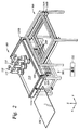
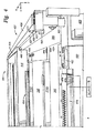
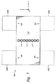
| US7535238B2 (en) * | 2005-04-29 | 2009-05-19 | Applied Materials, Inc. | In-line electron beam test system |
| TWI323788B (en) * | 2006-03-14 | 2010-04-21 | Applied Materials Inc | Method to reduce cross talk in a multi column e-beam test system |
| US7786742B2 (en) * | 2006-05-31 | 2010-08-31 | Applied Materials, Inc. | Prober for electronic device testing on large area substrates |
-
2006
- 2006-03-14 US US11/375,625 patent/US7535238B2/en active Active
- 2006-04-11 TW TW095112879A patent/TWI277759B/zh active
- 2006-04-28 KR KR1020060038828A patent/KR101255750B1/ko active Active
- 2006-04-28 JP JP2006125815A patent/JP2006317437A/ja active Pending
- 2006-04-29 CN CN2006100790744A patent/CN1854743B/zh active Active
-
2009
- 2009-04-10 US US12/422,164 patent/US7746088B2/en active Active
-
2010
- 2010-06-29 US US12/826,635 patent/US7973546B2/en active Active
Patent Citations (7)
| Publication number | Priority date | Publication date | Assignee | Title |
|---|---|---|---|---|
| JPH11265678A (ja) * | 1998-01-12 | 1999-09-28 | Shimadzu Corp | 基板検査用高速電子線計測装置及び基板検査方法 |
| JP2004309488A (ja) * | 1998-01-12 | 2004-11-04 | Shimadzu Corp | Tftfpd基板検査装置および検査方法 |
| JP2000003142A (ja) * | 1998-02-04 | 2000-01-07 | Shimadzu Corp | 電子線によるフラットパネルディスプレイのピクセル検査方法及び検査装置 |
| JP2004271516A (ja) * | 2003-03-04 | 2004-09-30 | Shimadzu Corp | 基板検査装置及び基板検査方法 |
| JP2004279163A (ja) * | 2003-03-14 | 2004-10-07 | Sony Corp | 基板検査装置及びその基板検査方法 |
| US6833717B1 (en) * | 2004-02-12 | 2004-12-21 | Applied Materials, Inc. | Electron beam test system with integrated substrate transfer module |
| JP2005227263A (ja) * | 2004-02-12 | 2005-08-25 | Applied Materials Inc | 集積基板搬送モジュールを備えた電子ビームテストシステム |
Also Published As
| Publication number | Publication date |
|---|---|
| TW200641376A (en) | 2006-12-01 |
| CN1854743B (zh) | 2012-12-12 |
| US7973546B2 (en) | 2011-07-05 |
| KR101255750B1 (ko) | 2013-04-17 |
| US20100327162A1 (en) | 2010-12-30 |
| US7535238B2 (en) | 2009-05-19 |
| CN1854743A (zh) | 2006-11-01 |
| US20060244467A1 (en) | 2006-11-02 |
| US7746088B2 (en) | 2010-06-29 |
| TWI277759B (en) | 2007-04-01 |
| US20090195262A1 (en) | 2009-08-06 |
| KR20060113545A (ko) | 2006-11-02 |
Similar Documents
| Publication | Publication Date | Title |
|---|---|---|
| US7973546B2 (en) | In-line electron beam test system | |
| US10823778B2 (en) | Inspection system | |
| KR100658258B1 (ko) | 기판 이송 모듈이 통합된 전자 빔 검사 시스템 | |
| KR100990002B1 (ko) | 대형 기판 테스트 시스템 | |
| KR101350662B1 (ko) | 디스플레이 셀들을 검사하기 위한 장치 | |
| KR20070115639A (ko) | 대면적 기판을 테스트하는 전자 장치용 프로버 | |
| KR101023890B1 (ko) | Tft-lcd 테스팅을 위한 소형 프로버 | |
| KR101854015B1 (ko) | 프로브 카드 수납 장치 | |
| US7786742B2 (en) | Prober for electronic device testing on large area substrates | |
| JP5047541B2 (ja) | 統合されたプローバドライブを備えた基板支持部 | |
| US20130278280A1 (en) | Apparatus and method for active voltage compensation of electrostatic discharge of a substrate | |
| KR101535726B1 (ko) | 디스플레이 셀들을 검사하기 위한 장치 | |
| KR101322164B1 (ko) | 디스플레이 셀들을 검사하기 위한 장치 | |
| US7602199B2 (en) | Mini-prober for TFT-LCD testing | |
| JP5527715B2 (ja) | 基板検査装置 | |
| KR20240117389A (ko) | 기판 처리 장치 및 로드락 챔버에서의 기판 검사 방법 | |
| US20060181266A1 (en) | Flat panel display inspection system | |
| KR20130051148A (ko) | 러빙 시스템 및 이를 위한 기판이송로봇 |
Legal Events
| Date | Code | Title | Description |
|---|---|---|---|
| A521 | Request for written amendment filed |
Free format text: JAPANESE INTERMEDIATE CODE: A523 Effective date: 20090428 |
|
| A621 | Written request for application examination |
Free format text: JAPANESE INTERMEDIATE CODE: A621 Effective date: 20090428 |
|
| A131 | Notification of reasons for refusal |
Free format text: JAPANESE INTERMEDIATE CODE: A131 Effective date: 20110628 |
|
| A977 | Report on retrieval |
Free format text: JAPANESE INTERMEDIATE CODE: A971007 Effective date: 20110630 |
|
| A601 | Written request for extension of time |
Free format text: JAPANESE INTERMEDIATE CODE: A601 Effective date: 20110928 |
|
| A602 | Written permission of extension of time |
Free format text: JAPANESE INTERMEDIATE CODE: A602 Effective date: 20111003 |
|
| A601 | Written request for extension of time |
Free format text: JAPANESE INTERMEDIATE CODE: A601 Effective date: 20111028 |
|
| A602 | Written permission of extension of time |
Free format text: JAPANESE INTERMEDIATE CODE: A602 Effective date: 20111102 |
|
| A601 | Written request for extension of time |
Free format text: JAPANESE INTERMEDIATE CODE: A601 Effective date: 20111128 |
|
| A602 | Written permission of extension of time |
Free format text: JAPANESE INTERMEDIATE CODE: A602 Effective date: 20111201 |
|
| A521 | Request for written amendment filed |
Free format text: JAPANESE INTERMEDIATE CODE: A523 Effective date: 20111220 |
|
| A131 | Notification of reasons for refusal |
Free format text: JAPANESE INTERMEDIATE CODE: A131 Effective date: 20120821 |
|
| A601 | Written request for extension of time |
Free format text: JAPANESE INTERMEDIATE CODE: A601 Effective date: 20121121 |
|
| A602 | Written permission of extension of time |
Free format text: JAPANESE INTERMEDIATE CODE: A602 Effective date: 20121127 |
|
| A601 | Written request for extension of time |
Free format text: JAPANESE INTERMEDIATE CODE: A601 Effective date: 20121220 |
|
| A602 | Written permission of extension of time |
Free format text: JAPANESE INTERMEDIATE CODE: A602 Effective date: 20121226 |
|
| A601 | Written request for extension of time |
Free format text: JAPANESE INTERMEDIATE CODE: A601 Effective date: 20130117 |
|
| A602 | Written permission of extension of time |
Free format text: JAPANESE INTERMEDIATE CODE: A602 Effective date: 20130122 |
|
| A02 | Decision of refusal |
Free format text: JAPANESE INTERMEDIATE CODE: A02 Effective date: 20130806 |