JP2005191240A - 半導体装置及びその製造方法 - Google Patents
半導体装置及びその製造方法 Download PDFInfo
- Publication number
- JP2005191240A JP2005191240A JP2003430092A JP2003430092A JP2005191240A JP 2005191240 A JP2005191240 A JP 2005191240A JP 2003430092 A JP2003430092 A JP 2003430092A JP 2003430092 A JP2003430092 A JP 2003430092A JP 2005191240 A JP2005191240 A JP 2005191240A
- Authority
- JP
- Japan
- Prior art keywords
- lead
- semiconductor device
- sealing body
- resin sealing
- recess
- Prior art date
- Legal status (The legal status is an assumption and is not a legal conclusion. Google has not performed a legal analysis and makes no representation as to the accuracy of the status listed.)
- Pending
Links
- 239000004065 semiconductor Substances 0.000 title claims abstract description 262
- 238000004519 manufacturing process Methods 0.000 title claims description 48
- 238000000034 method Methods 0.000 title claims description 43
- 239000011347 resin Substances 0.000 claims abstract description 155
- 229920005989 resin Polymers 0.000 claims abstract description 155
- 238000007789 sealing Methods 0.000 claims abstract description 128
- 229910000679 solder Inorganic materials 0.000 claims abstract description 46
- 238000007747 plating Methods 0.000 claims abstract description 40
- 238000005520 cutting process Methods 0.000 claims description 33
- 238000005516 engineering process Methods 0.000 abstract 2
- 230000000994 depressogenic effect Effects 0.000 abstract 1
- 239000000463 material Substances 0.000 description 32
- 230000015572 biosynthetic process Effects 0.000 description 23
- 238000000465 moulding Methods 0.000 description 23
- 239000000725 suspension Substances 0.000 description 14
- 230000013011 mating Effects 0.000 description 13
- 238000001721 transfer moulding Methods 0.000 description 11
- 239000000758 substrate Substances 0.000 description 7
- 238000010586 diagram Methods 0.000 description 6
- 230000000694 effects Effects 0.000 description 5
- 238000005476 soldering Methods 0.000 description 5
- 239000000853 adhesive Substances 0.000 description 4
- 230000001070 adhesive effect Effects 0.000 description 4
- 238000005530 etching Methods 0.000 description 4
- 229920001187 thermosetting polymer Polymers 0.000 description 4
- 239000010949 copper Substances 0.000 description 3
- 238000009713 electroplating Methods 0.000 description 3
- 230000017525 heat dissipation Effects 0.000 description 3
- 238000002347 injection Methods 0.000 description 3
- 239000007924 injection Substances 0.000 description 3
- 239000000203 mixture Substances 0.000 description 3
- PXHVJJICTQNCMI-UHFFFAOYSA-N nickel Substances [Ni] PXHVJJICTQNCMI-UHFFFAOYSA-N 0.000 description 3
- 241000587161 Gomphocarpus Species 0.000 description 2
- XEEYBQQBJWHFJM-UHFFFAOYSA-N Iron Chemical compound [Fe] XEEYBQQBJWHFJM-UHFFFAOYSA-N 0.000 description 2
- 229910020830 Sn-Bi Inorganic materials 0.000 description 2
- 229910018728 Sn—Bi Inorganic materials 0.000 description 2
- 229910045601 alloy Inorganic materials 0.000 description 2
- 239000000956 alloy Substances 0.000 description 2
- 230000007547 defect Effects 0.000 description 2
- ZUOUZKKEUPVFJK-UHFFFAOYSA-N diphenyl Chemical compound C1=CC=CC=C1C1=CC=CC=C1 ZUOUZKKEUPVFJK-UHFFFAOYSA-N 0.000 description 2
- 239000010931 gold Substances 0.000 description 2
- 239000002184 metal Substances 0.000 description 2
- 229910052751 metal Inorganic materials 0.000 description 2
- 230000004048 modification Effects 0.000 description 2
- 238000012986 modification Methods 0.000 description 2
- 238000003825 pressing Methods 0.000 description 2
- 230000001681 protective effect Effects 0.000 description 2
- 238000004904 shortening Methods 0.000 description 2
- RYGMFSIKBFXOCR-UHFFFAOYSA-N Copper Chemical compound [Cu] RYGMFSIKBFXOCR-UHFFFAOYSA-N 0.000 description 1
- 239000004593 Epoxy Substances 0.000 description 1
- 235000014676 Phragmites communis Nutrition 0.000 description 1
- ATJFFYVFTNAWJD-UHFFFAOYSA-N Tin Chemical compound [Sn] ATJFFYVFTNAWJD-UHFFFAOYSA-N 0.000 description 1
- 238000005452 bending Methods 0.000 description 1
- 235000010290 biphenyl Nutrition 0.000 description 1
- 239000004305 biphenyl Substances 0.000 description 1
- 229910052797 bismuth Inorganic materials 0.000 description 1
- JCXGWMGPZLAOME-UHFFFAOYSA-N bismuth atom Chemical compound [Bi] JCXGWMGPZLAOME-UHFFFAOYSA-N 0.000 description 1
- 239000003795 chemical substances by application Substances 0.000 description 1
- 229910052802 copper Inorganic materials 0.000 description 1
- 230000007423 decrease Effects 0.000 description 1
- 239000000945 filler Substances 0.000 description 1
- PCHJSUWPFVWCPO-UHFFFAOYSA-N gold Chemical compound [Au] PCHJSUWPFVWCPO-UHFFFAOYSA-N 0.000 description 1
- 229910052737 gold Inorganic materials 0.000 description 1
- 238000010438 heat treatment Methods 0.000 description 1
- 229910052742 iron Inorganic materials 0.000 description 1
- 230000007257 malfunction Effects 0.000 description 1
- 239000011159 matrix material Substances 0.000 description 1
- 229910052759 nickel Inorganic materials 0.000 description 1
- 230000002093 peripheral effect Effects 0.000 description 1
- ISWSIDIOOBJBQZ-UHFFFAOYSA-N phenol group Chemical group C1(=CC=CC=C1)O ISWSIDIOOBJBQZ-UHFFFAOYSA-N 0.000 description 1
- 230000002265 prevention Effects 0.000 description 1
- 238000004080 punching Methods 0.000 description 1
- 230000003252 repetitive effect Effects 0.000 description 1
- 239000012260 resinous material Substances 0.000 description 1
- 238000007650 screen-printing Methods 0.000 description 1
- 238000010008 shearing Methods 0.000 description 1
- 229920002379 silicone rubber Polymers 0.000 description 1
- 239000004945 silicone rubber Substances 0.000 description 1
- 230000000087 stabilizing effect Effects 0.000 description 1
- 238000009736 wetting Methods 0.000 description 1
Images


Classifications
-
- H—ELECTRICITY
- H01—ELECTRIC ELEMENTS
- H01L—SEMICONDUCTOR DEVICES NOT COVERED BY CLASS H10
- H01L23/00—Details of semiconductor or other solid state devices
- H01L23/48—Arrangements for conducting electric current to or from the solid state body in operation, e.g. leads, terminal arrangements ; Selection of materials therefor
- H01L23/488—Arrangements for conducting electric current to or from the solid state body in operation, e.g. leads, terminal arrangements ; Selection of materials therefor consisting of soldered or bonded constructions
- H01L23/495—Lead-frames or other flat leads
- H01L23/49541—Geometry of the lead-frame
- H01L23/49548—Cross section geometry
-
- H—ELECTRICITY
- H01—ELECTRIC ELEMENTS
- H01L—SEMICONDUCTOR DEVICES NOT COVERED BY CLASS H10
- H01L23/00—Details of semiconductor or other solid state devices
- H01L23/52—Arrangements for conducting electric current within the device in operation from one component to another, i.e. interconnections, e.g. wires, lead frames
-
- H—ELECTRICITY
- H01—ELECTRIC ELEMENTS
- H01L—SEMICONDUCTOR DEVICES NOT COVERED BY CLASS H10
- H01L21/00—Processes or apparatus adapted for the manufacture or treatment of semiconductor or solid state devices or of parts thereof
- H01L21/02—Manufacture or treatment of semiconductor devices or of parts thereof
- H01L21/04—Manufacture or treatment of semiconductor devices or of parts thereof the devices having potential barriers, e.g. a PN junction, depletion layer or carrier concentration layer
- H01L21/50—Assembly of semiconductor devices using processes or apparatus not provided for in a single one of the subgroups H01L21/06 - H01L21/326, e.g. sealing of a cap to a base of a container
- H01L21/56—Encapsulations, e.g. encapsulation layers, coatings
- H01L21/565—Moulds
-
- H—ELECTRICITY
- H01—ELECTRIC ELEMENTS
- H01L—SEMICONDUCTOR DEVICES NOT COVERED BY CLASS H10
- H01L23/00—Details of semiconductor or other solid state devices
- H01L23/28—Encapsulations, e.g. encapsulating layers, coatings, e.g. for protection
- H01L23/31—Encapsulations, e.g. encapsulating layers, coatings, e.g. for protection characterised by the arrangement or shape
- H01L23/3107—Encapsulations, e.g. encapsulating layers, coatings, e.g. for protection characterised by the arrangement or shape the device being completely enclosed
-
- H—ELECTRICITY
- H01—ELECTRIC ELEMENTS
- H01L—SEMICONDUCTOR DEVICES NOT COVERED BY CLASS H10
- H01L24/00—Arrangements for connecting or disconnecting semiconductor or solid-state bodies; Methods or apparatus related thereto
- H01L24/93—Batch processes
- H01L24/95—Batch processes at chip-level, i.e. with connecting carried out on a plurality of singulated devices, i.e. on diced chips
- H01L24/97—Batch processes at chip-level, i.e. with connecting carried out on a plurality of singulated devices, i.e. on diced chips the devices being connected to a common substrate, e.g. interposer, said common substrate being separable into individual assemblies after connecting
-
- H—ELECTRICITY
- H01—ELECTRIC ELEMENTS
- H01L—SEMICONDUCTOR DEVICES NOT COVERED BY CLASS H10
- H01L2224/00—Indexing scheme for arrangements for connecting or disconnecting semiconductor or solid-state bodies and methods related thereto as covered by H01L24/00
- H01L2224/01—Means for bonding being attached to, or being formed on, the surface to be connected, e.g. chip-to-package, die-attach, "first-level" interconnects; Manufacturing methods related thereto
- H01L2224/02—Bonding areas; Manufacturing methods related thereto
- H01L2224/04—Structure, shape, material or disposition of the bonding areas prior to the connecting process
- H01L2224/05—Structure, shape, material or disposition of the bonding areas prior to the connecting process of an individual bonding area
- H01L2224/0554—External layer
- H01L2224/0555—Shape
- H01L2224/05552—Shape in top view
- H01L2224/05554—Shape in top view being square
-
- H—ELECTRICITY
- H01—ELECTRIC ELEMENTS
- H01L—SEMICONDUCTOR DEVICES NOT COVERED BY CLASS H10
- H01L2224/00—Indexing scheme for arrangements for connecting or disconnecting semiconductor or solid-state bodies and methods related thereto as covered by H01L24/00
- H01L2224/01—Means for bonding being attached to, or being formed on, the surface to be connected, e.g. chip-to-package, die-attach, "first-level" interconnects; Manufacturing methods related thereto
- H01L2224/26—Layer connectors, e.g. plate connectors, solder or adhesive layers; Manufacturing methods related thereto
- H01L2224/31—Structure, shape, material or disposition of the layer connectors after the connecting process
- H01L2224/32—Structure, shape, material or disposition of the layer connectors after the connecting process of an individual layer connector
- H01L2224/3201—Structure
- H01L2224/32012—Structure relative to the bonding area, e.g. bond pad
- H01L2224/32014—Structure relative to the bonding area, e.g. bond pad the layer connector being smaller than the bonding area, e.g. bond pad
-
- H—ELECTRICITY
- H01—ELECTRIC ELEMENTS
- H01L—SEMICONDUCTOR DEVICES NOT COVERED BY CLASS H10
- H01L2224/00—Indexing scheme for arrangements for connecting or disconnecting semiconductor or solid-state bodies and methods related thereto as covered by H01L24/00
- H01L2224/01—Means for bonding being attached to, or being formed on, the surface to be connected, e.g. chip-to-package, die-attach, "first-level" interconnects; Manufacturing methods related thereto
- H01L2224/26—Layer connectors, e.g. plate connectors, solder or adhesive layers; Manufacturing methods related thereto
- H01L2224/31—Structure, shape, material or disposition of the layer connectors after the connecting process
- H01L2224/32—Structure, shape, material or disposition of the layer connectors after the connecting process of an individual layer connector
- H01L2224/321—Disposition
- H01L2224/32151—Disposition the layer connector connecting between a semiconductor or solid-state body and an item not being a semiconductor or solid-state body, e.g. chip-to-substrate, chip-to-passive
- H01L2224/32221—Disposition the layer connector connecting between a semiconductor or solid-state body and an item not being a semiconductor or solid-state body, e.g. chip-to-substrate, chip-to-passive the body and the item being stacked
- H01L2224/32245—Disposition the layer connector connecting between a semiconductor or solid-state body and an item not being a semiconductor or solid-state body, e.g. chip-to-substrate, chip-to-passive the body and the item being stacked the item being metallic
-
- H—ELECTRICITY
- H01—ELECTRIC ELEMENTS
- H01L—SEMICONDUCTOR DEVICES NOT COVERED BY CLASS H10
- H01L2224/00—Indexing scheme for arrangements for connecting or disconnecting semiconductor or solid-state bodies and methods related thereto as covered by H01L24/00
- H01L2224/01—Means for bonding being attached to, or being formed on, the surface to be connected, e.g. chip-to-package, die-attach, "first-level" interconnects; Manufacturing methods related thereto
- H01L2224/42—Wire connectors; Manufacturing methods related thereto
- H01L2224/44—Structure, shape, material or disposition of the wire connectors prior to the connecting process
- H01L2224/45—Structure, shape, material or disposition of the wire connectors prior to the connecting process of an individual wire connector
- H01L2224/45001—Core members of the connector
- H01L2224/4501—Shape
- H01L2224/45012—Cross-sectional shape
- H01L2224/45015—Cross-sectional shape being circular
-
- H—ELECTRICITY
- H01—ELECTRIC ELEMENTS
- H01L—SEMICONDUCTOR DEVICES NOT COVERED BY CLASS H10
- H01L2224/00—Indexing scheme for arrangements for connecting or disconnecting semiconductor or solid-state bodies and methods related thereto as covered by H01L24/00
- H01L2224/01—Means for bonding being attached to, or being formed on, the surface to be connected, e.g. chip-to-package, die-attach, "first-level" interconnects; Manufacturing methods related thereto
- H01L2224/42—Wire connectors; Manufacturing methods related thereto
- H01L2224/44—Structure, shape, material or disposition of the wire connectors prior to the connecting process
- H01L2224/45—Structure, shape, material or disposition of the wire connectors prior to the connecting process of an individual wire connector
- H01L2224/45001—Core members of the connector
- H01L2224/45099—Material
- H01L2224/451—Material with a principal constituent of the material being a metal or a metalloid, e.g. boron (B), silicon (Si), germanium (Ge), arsenic (As), antimony (Sb), tellurium (Te) and polonium (Po), and alloys thereof
- H01L2224/45138—Material with a principal constituent of the material being a metal or a metalloid, e.g. boron (B), silicon (Si), germanium (Ge), arsenic (As), antimony (Sb), tellurium (Te) and polonium (Po), and alloys thereof the principal constituent melting at a temperature of greater than or equal to 950°C and less than 1550°C
- H01L2224/45144—Gold (Au) as principal constituent
-
- H—ELECTRICITY
- H01—ELECTRIC ELEMENTS
- H01L—SEMICONDUCTOR DEVICES NOT COVERED BY CLASS H10
- H01L2224/00—Indexing scheme for arrangements for connecting or disconnecting semiconductor or solid-state bodies and methods related thereto as covered by H01L24/00
- H01L2224/01—Means for bonding being attached to, or being formed on, the surface to be connected, e.g. chip-to-package, die-attach, "first-level" interconnects; Manufacturing methods related thereto
- H01L2224/42—Wire connectors; Manufacturing methods related thereto
- H01L2224/47—Structure, shape, material or disposition of the wire connectors after the connecting process
- H01L2224/48—Structure, shape, material or disposition of the wire connectors after the connecting process of an individual wire connector
- H01L2224/4805—Shape
- H01L2224/4809—Loop shape
- H01L2224/48095—Kinked
-
- H—ELECTRICITY
- H01—ELECTRIC ELEMENTS
- H01L—SEMICONDUCTOR DEVICES NOT COVERED BY CLASS H10
- H01L2224/00—Indexing scheme for arrangements for connecting or disconnecting semiconductor or solid-state bodies and methods related thereto as covered by H01L24/00
- H01L2224/01—Means for bonding being attached to, or being formed on, the surface to be connected, e.g. chip-to-package, die-attach, "first-level" interconnects; Manufacturing methods related thereto
- H01L2224/42—Wire connectors; Manufacturing methods related thereto
- H01L2224/47—Structure, shape, material or disposition of the wire connectors after the connecting process
- H01L2224/48—Structure, shape, material or disposition of the wire connectors after the connecting process of an individual wire connector
- H01L2224/481—Disposition
- H01L2224/48151—Connecting between a semiconductor or solid-state body and an item not being a semiconductor or solid-state body, e.g. chip-to-substrate, chip-to-passive
- H01L2224/48221—Connecting between a semiconductor or solid-state body and an item not being a semiconductor or solid-state body, e.g. chip-to-substrate, chip-to-passive the body and the item being stacked
- H01L2224/48245—Connecting between a semiconductor or solid-state body and an item not being a semiconductor or solid-state body, e.g. chip-to-substrate, chip-to-passive the body and the item being stacked the item being metallic
- H01L2224/48247—Connecting between a semiconductor or solid-state body and an item not being a semiconductor or solid-state body, e.g. chip-to-substrate, chip-to-passive the body and the item being stacked the item being metallic connecting the wire to a bond pad of the item
-
- H—ELECTRICITY
- H01—ELECTRIC ELEMENTS
- H01L—SEMICONDUCTOR DEVICES NOT COVERED BY CLASS H10
- H01L2224/00—Indexing scheme for arrangements for connecting or disconnecting semiconductor or solid-state bodies and methods related thereto as covered by H01L24/00
- H01L2224/01—Means for bonding being attached to, or being formed on, the surface to be connected, e.g. chip-to-package, die-attach, "first-level" interconnects; Manufacturing methods related thereto
- H01L2224/42—Wire connectors; Manufacturing methods related thereto
- H01L2224/47—Structure, shape, material or disposition of the wire connectors after the connecting process
- H01L2224/49—Structure, shape, material or disposition of the wire connectors after the connecting process of a plurality of wire connectors
- H01L2224/491—Disposition
- H01L2224/4912—Layout
- H01L2224/49171—Fan-out arrangements
-
- H—ELECTRICITY
- H01—ELECTRIC ELEMENTS
- H01L—SEMICONDUCTOR DEVICES NOT COVERED BY CLASS H10
- H01L2224/00—Indexing scheme for arrangements for connecting or disconnecting semiconductor or solid-state bodies and methods related thereto as covered by H01L24/00
- H01L2224/73—Means for bonding being of different types provided for in two or more of groups H01L2224/10, H01L2224/18, H01L2224/26, H01L2224/34, H01L2224/42, H01L2224/50, H01L2224/63, H01L2224/71
- H01L2224/732—Location after the connecting process
- H01L2224/73251—Location after the connecting process on different surfaces
- H01L2224/73265—Layer and wire connectors
-
- H—ELECTRICITY
- H01—ELECTRIC ELEMENTS
- H01L—SEMICONDUCTOR DEVICES NOT COVERED BY CLASS H10
- H01L2224/00—Indexing scheme for arrangements for connecting or disconnecting semiconductor or solid-state bodies and methods related thereto as covered by H01L24/00
- H01L2224/91—Methods for connecting semiconductor or solid state bodies including different methods provided for in two or more of groups H01L2224/80 - H01L2224/90
- H01L2224/92—Specific sequence of method steps
- H01L2224/922—Connecting different surfaces of the semiconductor or solid-state body with connectors of different types
- H01L2224/9222—Sequential connecting processes
- H01L2224/92242—Sequential connecting processes the first connecting process involving a layer connector
- H01L2224/92247—Sequential connecting processes the first connecting process involving a layer connector the second connecting process involving a wire connector
-
- H—ELECTRICITY
- H01—ELECTRIC ELEMENTS
- H01L—SEMICONDUCTOR DEVICES NOT COVERED BY CLASS H10
- H01L2224/00—Indexing scheme for arrangements for connecting or disconnecting semiconductor or solid-state bodies and methods related thereto as covered by H01L24/00
- H01L2224/93—Batch processes
- H01L2224/95—Batch processes at chip-level, i.e. with connecting carried out on a plurality of singulated devices, i.e. on diced chips
- H01L2224/97—Batch processes at chip-level, i.e. with connecting carried out on a plurality of singulated devices, i.e. on diced chips the devices being connected to a common substrate, e.g. interposer, said common substrate being separable into individual assemblies after connecting
-
- H—ELECTRICITY
- H01—ELECTRIC ELEMENTS
- H01L—SEMICONDUCTOR DEVICES NOT COVERED BY CLASS H10
- H01L24/00—Arrangements for connecting or disconnecting semiconductor or solid-state bodies; Methods or apparatus related thereto
- H01L24/01—Means for bonding being attached to, or being formed on, the surface to be connected, e.g. chip-to-package, die-attach, "first-level" interconnects; Manufacturing methods related thereto
- H01L24/42—Wire connectors; Manufacturing methods related thereto
- H01L24/44—Structure, shape, material or disposition of the wire connectors prior to the connecting process
- H01L24/45—Structure, shape, material or disposition of the wire connectors prior to the connecting process of an individual wire connector
-
- H—ELECTRICITY
- H01—ELECTRIC ELEMENTS
- H01L—SEMICONDUCTOR DEVICES NOT COVERED BY CLASS H10
- H01L24/00—Arrangements for connecting or disconnecting semiconductor or solid-state bodies; Methods or apparatus related thereto
- H01L24/01—Means for bonding being attached to, or being formed on, the surface to be connected, e.g. chip-to-package, die-attach, "first-level" interconnects; Manufacturing methods related thereto
- H01L24/42—Wire connectors; Manufacturing methods related thereto
- H01L24/47—Structure, shape, material or disposition of the wire connectors after the connecting process
- H01L24/48—Structure, shape, material or disposition of the wire connectors after the connecting process of an individual wire connector
-
- H—ELECTRICITY
- H01—ELECTRIC ELEMENTS
- H01L—SEMICONDUCTOR DEVICES NOT COVERED BY CLASS H10
- H01L24/00—Arrangements for connecting or disconnecting semiconductor or solid-state bodies; Methods or apparatus related thereto
- H01L24/01—Means for bonding being attached to, or being formed on, the surface to be connected, e.g. chip-to-package, die-attach, "first-level" interconnects; Manufacturing methods related thereto
- H01L24/42—Wire connectors; Manufacturing methods related thereto
- H01L24/47—Structure, shape, material or disposition of the wire connectors after the connecting process
- H01L24/49—Structure, shape, material or disposition of the wire connectors after the connecting process of a plurality of wire connectors
-
- H—ELECTRICITY
- H01—ELECTRIC ELEMENTS
- H01L—SEMICONDUCTOR DEVICES NOT COVERED BY CLASS H10
- H01L2924/00—Indexing scheme for arrangements or methods for connecting or disconnecting semiconductor or solid-state bodies as covered by H01L24/00
- H01L2924/0001—Technical content checked by a classifier
- H01L2924/00014—Technical content checked by a classifier the subject-matter covered by the group, the symbol of which is combined with the symbol of this group, being disclosed without further technical details
-
- H—ELECTRICITY
- H01—ELECTRIC ELEMENTS
- H01L—SEMICONDUCTOR DEVICES NOT COVERED BY CLASS H10
- H01L2924/00—Indexing scheme for arrangements or methods for connecting or disconnecting semiconductor or solid-state bodies as covered by H01L24/00
- H01L2924/01—Chemical elements
- H01L2924/01005—Boron [B]
-
- H—ELECTRICITY
- H01—ELECTRIC ELEMENTS
- H01L—SEMICONDUCTOR DEVICES NOT COVERED BY CLASS H10
- H01L2924/00—Indexing scheme for arrangements or methods for connecting or disconnecting semiconductor or solid-state bodies as covered by H01L24/00
- H01L2924/01—Chemical elements
- H01L2924/01006—Carbon [C]
-
- H—ELECTRICITY
- H01—ELECTRIC ELEMENTS
- H01L—SEMICONDUCTOR DEVICES NOT COVERED BY CLASS H10
- H01L2924/00—Indexing scheme for arrangements or methods for connecting or disconnecting semiconductor or solid-state bodies as covered by H01L24/00
- H01L2924/01—Chemical elements
- H01L2924/01027—Cobalt [Co]
-
- H—ELECTRICITY
- H01—ELECTRIC ELEMENTS
- H01L—SEMICONDUCTOR DEVICES NOT COVERED BY CLASS H10
- H01L2924/00—Indexing scheme for arrangements or methods for connecting or disconnecting semiconductor or solid-state bodies as covered by H01L24/00
- H01L2924/01—Chemical elements
- H01L2924/01029—Copper [Cu]
-
- H—ELECTRICITY
- H01—ELECTRIC ELEMENTS
- H01L—SEMICONDUCTOR DEVICES NOT COVERED BY CLASS H10
- H01L2924/00—Indexing scheme for arrangements or methods for connecting or disconnecting semiconductor or solid-state bodies as covered by H01L24/00
- H01L2924/01—Chemical elements
- H01L2924/01033—Arsenic [As]
-
- H—ELECTRICITY
- H01—ELECTRIC ELEMENTS
- H01L—SEMICONDUCTOR DEVICES NOT COVERED BY CLASS H10
- H01L2924/00—Indexing scheme for arrangements or methods for connecting or disconnecting semiconductor or solid-state bodies as covered by H01L24/00
- H01L2924/01—Chemical elements
- H01L2924/01078—Platinum [Pt]
-
- H—ELECTRICITY
- H01—ELECTRIC ELEMENTS
- H01L—SEMICONDUCTOR DEVICES NOT COVERED BY CLASS H10
- H01L2924/00—Indexing scheme for arrangements or methods for connecting or disconnecting semiconductor or solid-state bodies as covered by H01L24/00
- H01L2924/01—Chemical elements
- H01L2924/01079—Gold [Au]
-
- H—ELECTRICITY
- H01—ELECTRIC ELEMENTS
- H01L—SEMICONDUCTOR DEVICES NOT COVERED BY CLASS H10
- H01L2924/00—Indexing scheme for arrangements or methods for connecting or disconnecting semiconductor or solid-state bodies as covered by H01L24/00
- H01L2924/01—Chemical elements
- H01L2924/01082—Lead [Pb]
-
- H—ELECTRICITY
- H01—ELECTRIC ELEMENTS
- H01L—SEMICONDUCTOR DEVICES NOT COVERED BY CLASS H10
- H01L2924/00—Indexing scheme for arrangements or methods for connecting or disconnecting semiconductor or solid-state bodies as covered by H01L24/00
- H01L2924/10—Details of semiconductor or other solid state devices to be connected
- H01L2924/11—Device type
- H01L2924/12—Passive devices, e.g. 2 terminal devices
- H01L2924/1204—Optical Diode
- H01L2924/12041—LED
-
- H—ELECTRICITY
- H01—ELECTRIC ELEMENTS
- H01L—SEMICONDUCTOR DEVICES NOT COVERED BY CLASS H10
- H01L2924/00—Indexing scheme for arrangements or methods for connecting or disconnecting semiconductor or solid-state bodies as covered by H01L24/00
- H01L2924/10—Details of semiconductor or other solid state devices to be connected
- H01L2924/11—Device type
- H01L2924/14—Integrated circuits
-
- H—ELECTRICITY
- H01—ELECTRIC ELEMENTS
- H01L—SEMICONDUCTOR DEVICES NOT COVERED BY CLASS H10
- H01L2924/00—Indexing scheme for arrangements or methods for connecting or disconnecting semiconductor or solid-state bodies as covered by H01L24/00
- H01L2924/15—Details of package parts other than the semiconductor or other solid state devices to be connected
- H01L2924/151—Die mounting substrate
- H01L2924/153—Connection portion
- H01L2924/1532—Connection portion the connection portion being formed on the die mounting surface of the substrate
-
- H—ELECTRICITY
- H01—ELECTRIC ELEMENTS
- H01L—SEMICONDUCTOR DEVICES NOT COVERED BY CLASS H10
- H01L2924/00—Indexing scheme for arrangements or methods for connecting or disconnecting semiconductor or solid-state bodies as covered by H01L24/00
- H01L2924/15—Details of package parts other than the semiconductor or other solid state devices to be connected
- H01L2924/181—Encapsulation
-
- H—ELECTRICITY
- H01—ELECTRIC ELEMENTS
- H01L—SEMICONDUCTOR DEVICES NOT COVERED BY CLASS H10
- H01L2924/00—Indexing scheme for arrangements or methods for connecting or disconnecting semiconductor or solid-state bodies as covered by H01L24/00
- H01L2924/19—Details of hybrid assemblies other than the semiconductor or other solid state devices to be connected
- H01L2924/1901—Structure
- H01L2924/1904—Component type
- H01L2924/19043—Component type being a resistor
Landscapes
- Engineering & Computer Science (AREA)
- Physics & Mathematics (AREA)
- Computer Hardware Design (AREA)
- Microelectronics & Electronic Packaging (AREA)
- Power Engineering (AREA)
- Condensed Matter Physics & Semiconductors (AREA)
- General Physics & Mathematics (AREA)
- Geometry (AREA)
- Manufacturing & Machinery (AREA)
- Lead Frames For Integrated Circuits (AREA)
- Encapsulation Of And Coatings For Semiconductor Or Solid State Devices (AREA)
- Structures Or Materials For Encapsulating Or Coating Semiconductor Devices Or Solid State Devices (AREA)
Abstract
【解決手段】 半導体装置のリードは、樹脂封止体の主面と前記主面とは反対側の裏面との間に位置する第1の面と、前記第1の面の反対側に位置し、かつ前記樹脂封止体の裏面から露出する第2の面と、半導体チップ側に位置する第1の先端面と、前記第1の先端面の反対側に位置し、かつ前記樹脂封止体の側面から露出する第2の先端面と、前記第2の面から前記第1の面側に窪み、かつ前記第2の先端面に連なる凹部とを有し、
前記第2の面及び前記凹部の内壁面は、前記リードの第2の先端面よりも半田濡れ性が高いメッキ層で覆われている。
【選択図】 図5
Description
前記半導体チップの複数の電極に夫々電気的に接続された複数のリードと、
前記半導体チップ、複数のリードを封止する樹脂封止体とを有し、
前記複数のリードは、前記樹脂封止体の主面と、前記主面とは反対側の裏面との間に位置する第1の面と、前記第1の面の反対側に位置し、前記樹脂封止体の裏面から露出する第2の面と、前記半導体チップ側に位置する第1の先端面と、前記第1の先端面の反対側に位置し、前記樹脂封止体の側面から突出する第2の先端面と、前記第2の面から前記第1の面側に窪み、前記第2の先端面に連通する凹部とを有し、
前記第2の面及び前記凹部の壁面は、前記リードの第2の先端面よりも半田濡れ性が高いメッキ層で覆われている。
本発明によれば、半導体装置の実装信頼性向上を図ることができる。
本発明によれば、半導体装置の小型化を図ることができる。
本実施形態1では、外部接続用端子部として樹脂封止体の裏面にリードを露出させるノンリード型半導体装置の一種であるQFN型半導体装置に本発明を適用した例について説明する。
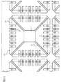
図1は、半導体装置の外観構造を示す模式的平面図(上面図)、
図2は、半導体装置の外観構造を示す模式的底面図(下面図)、
図3は、図2の一部を拡大した模式的底面図(下面図)、
図4は、半導体装置の内部構造を示す図((a)は樹脂封止体の上部を除去した状態の模式的平面図,(b)は(a)のa−a線に沿う模式的断面図)、
図5は、図4(b)の一部を拡大した模式的断面図、
図6は、半導体装置の外観構造の一部を示す模式的側面図、
図7は、図5のリードの裏面側を示す模式的斜視図、
図8は、半導体装置の製造に使用されるリードフレームの一部を示す模式的平面図(上面図)、
図9は、図8の一部を拡大した模式的平面図、
図10は、図9のb−b線に沿う模式的断面図、
図11は、図9の反対側の裏面を示す模式的底面図(下面図)である。
図13は、図12に続く樹脂封止工程を示す図((a)は成形金型にリードフレームを位置決めした状態を示す模式的断面図,(b)は樹脂封止した状態を示す模式的断面図)、
図14は、図13(a)の一部を拡大した模式的断面図、
図15は、図13に続くメッキ工程を示す模式的断面図、
図16は、図15に続く切断工程を示す模式的断面図、
図17は、半導体装置を実装した状態を示す模式的断面図、
図18は、図17の一部を拡大した模式的断面図である。
また、リードフレームLFの位置決めは、リードフレームLFの各製品形成領域16毎に設けられた各々のキャビティ21の内部において、半導体チップ2、リード5、チップ支持体7、吊りリード7a、ボンディングワイヤ8等が位置する状態で行われる。
また、リードフレームLFの位置決めは、キャビティ21と上型20aの合わせ面に亘ってリード5が位置し、リード5の非封止部分が上型20aの合わせ面と下型20bの合わせ面との間に位置する状態で行われる。
また、リードフレームLFの位置決めは、リード5の非封止部分、及びこのリード5の非封止部分と対応するシート22の部分を上型20aの合わせ面と下型20bの合わせ面とで上下方向から締め付ける(押さえる)ことによって行われる。
また、リードフレームLFの位置決めは、リード5がシート22に食い込むように、上型20aと下型20bとの締め付け力(クランプ力,挟み力)によってシート22を潰した状態で行われる。
本実施形態2では、リードに抜け防止手段を設けた半導体装置に本発明を適用した例について説明する。
図20は、図19のリードの模式的底面図(下面図)である。
本実施形態3では、リードに設けられる凹部の形状を変えた第1の変形例について説明する。
図22は、図21のリードの模式的底面図(下面図)である。
本実施形態4では、リードに設けられる凹部の形状を変えた第2の変形例について説明する。
図24は、図23のリードの模式的底面図(下面図)である。
本実施形態5では、リードに設けられる凹部の形状を変えた第3の変形例について説明する。
図26は、図25のリードの模式的底面図(下面図)である。
本実施形態6では、樹脂封止体の裏面からチップ支持体を露出させた半導体装置に本発明を適用した例について説明する。
図28は、図27のc−c線に沿う要部模式的断面図である。
本実施形態7では、フェィスダウン構造のQFN型半導体装置に本発明を適用した例について説明する。
前述の実施形態1では、個別方式のトランスファモールディング法を用いて半導体装置を製造する例について説明したが、本実施形態8では、一括方式の戸欄ファモールディング法で半導体装置を製造する例について説明する。
図31は、図30(b)の一部を拡大した模式的断面図、
図32は、本実施形態8の半導体装置の製造に使用されるリードフレームの模式的平面図、
図33は、図32の一部を拡大して裏面側を示す模式的底面図、
図34は、本実施形態8の半導体装置の製造工程を示す図((a)はワイヤボンディング工程を示す模式的断面図,(b)は樹脂封止工程を示す模式的断面図)、
図35は、図34に続く半導体装置の製造工程を示す図((a)はメッキ工程を示す模式的断面図,(b)は切断工程を示す模式的断面図)、
図36は、図35(b)に示す樹脂封止工程において形成された樹脂封止体を示す模式的平面図である。
(実施形態9)
本実施形態9では、チップ支持体7が樹脂封止体9の主面9xに露出するQON(Quad Out-line Non-leaded Package)型半導体装置に本発明を適用した例について説明する。
Claims (26)
- 互いに反対側に位置する主面及び裏面と、前記主面に配置された複数の電極とを有する半導体チップと、
前記半導体チップの複数の電極に夫々電気的に接続された複数のリードと、
前記半導体チップ、前記複数のリードを封止する樹脂封止体とを有し、
前記複数のリードは、前記樹脂封止体の主面と、前記主面とは反対側の裏面との間に位置する第1の面と、
前記第1の面の反対側に位置し、かつ前記樹脂封止体の裏面から露出する第2の面と、
前記半導体チップ側に位置する第1の先端面と、
前記第1の先端面の反対側に位置し、かつ前記樹脂封止体の側面から露出する第2の先端面と、
前記第2の面から前記第1の面側に窪み、かつ前記第2の先端面に連なる凹部とを有し、
前記第2の面及び前記凹部の内壁面は、前記リードの前記第2の先端面よりも半田濡れ性が高いメッキ層で覆われていることを特徴とする半導体装置。 - 請求項1に記載の半導体装置において、
前記凹部は、前記リードの第2の先端面で終端し、前記第2の先端面から露出していることを特徴とする半導体装置。 - 請求項1に記載の半導体装置において、
前記メッキ層は、前記リードの第2の先端面で終端し、前記第2の先端面から露出していることを特徴とする半導体装置。 - 請求項1に記載の半導体装置において、
前記凹部は、前記リードの幅方向において互いに反対側に位置する前記リードの2つの側面から離間して設けられていることを特徴とする半導体装置。 - 請求項1に記載の半導体装置において、
前記第2の先端面は、切断面であることを特徴とする半導体装置。 - 請求項1に記載の半導体装置において、
前記第1及び第2の面は、前記第2の先端面に連なり、
前記第2の先端面は、前記樹脂封止体の側面から突出していることを特徴とする半導体装置。 - 請求項6に記載の半導体装置において、
前記凹部は、前記樹脂封止体の外側に設けられていることを特徴とする半導体装置。 - 請求項1に記載の半導体装置において、
前記凹部は、前記樹脂封止体の側面の外側と内側に亘って設けられていることを特徴とする半導体装置。 - 請求項1に記載の半導体装置において、
更に、前記半導体チップの複数の電極と前記複数のリードの第1の面とを夫々電気的に接続する複数のボンディングワイヤを有することを特徴とする半導体装置。 - 請求項9に記載の半導体装置において、
更に、前記リードよりも厚さが薄いチップ支持体を有し、
前記半導体チップは、その裏面が前記チップ支持体の第1の面に接着され、
前記チップ支持体の第1の面と反対側の第2の面は、前記樹脂封止体の樹脂で覆われていることを特徴とする半導体装置。 - 請求項1に記載の半導体装置において、
更に、チップ支持体を有し、
前記チップ支持体は、前記半導体チップが接着された第1の面と、前記第1の面の反対側に位置し、かつ前記樹脂封止体の裏面から露出する第2の面と、前記第2の面から前記第1の面側に窪み、かつ前記樹脂封止体の裏面から露出する凹部とを有することを特徴とする半導体装置。 - 請求項1に記載の半導体装置において、
半導体チップの複数の電極は、前記複数のリードの第1の面に突起状電極を介在して夫々電気的に接続されていることを特徴とする半導体装置。 - 互いに反対側に位置する主面及び裏面と、前記主面に配置された複数の電極とを有する半導体チップと、
前記半導体チップの複数の電極に夫々電気的に接続された複数のリードと、
前記半導体チップ、前記複数のリードを封止する樹脂封止体とを有し、
前記複数のリードは、前記樹脂封止体の主面と前記主面とは反対側に裏面との間に位置する第1の面と、
前記第1の面の反対側に位置し、かつ前記樹脂封止体の裏面から露出する第2の面と、
前記第2の面から前記第1の面側に窪む凹部とを有し、
前記第2の面及び前記凹部の内壁面は、前記リードの第2の先端面よりも半田濡れ性が高いメッキ層で覆われていることを特徴とする半導体装置。 - 請求項13に記載の半導体装置において、
前記凹部は、複数設けられていることを特徴とする半導体装置。 - 互いに反対側に位置する主面及び裏面と、前記主面に配置された複数の電極とを有する半導体チップと、
前記半導体チップの複数の電極に夫々電気的に接続された複数のリードと、
前記半導体チップ、複数のリードを封止する樹脂封止体とを有し、
前記複数のリードは、前記樹脂封止体の主面と前記樹脂封止体の主面とは反対側の裏面との間に位置する第1の面と、
前記第1の面の反対側に位置し、かつ前記樹脂封止体の裏面から露出する第2の面と、
前記半導体チップ側に位置する第1の先端面と、
前記第1の先端面の反対側に位置し、かつ前記樹脂封止体の側面から露出する第2の先端面と、
前記第2の面から前記第1の面側に窪む複数の凹部とを有し、
前記複数の凹部の中の少なくとも1つは、前記リードの第2の先端面に連なっており、
前記第2の面、及び前記複数の凹部の各々の内壁面は、前記リードの前記第2の先端面よりも半田濡れ性が高いメッキ層で覆われていることを特徴とする半導体装置。 - 請求項15に記載の半導体装置において、
前記第1及び第2の面は、前記第2の先端面に連なり、
前記第2の先端面は、前記樹脂封止体の側面から突出し、
前記複数の凹部は、前記樹脂封止体の側面の外側と内側に亘って点在していることを特徴とする半導体装置。 - 樹脂封止体で封止された半導体チップ及びリードを有し、前記リードは、前記樹脂封止体の内外に亘って延在し、かつ前記樹脂封止体の側面から突出する第1の面と、前記第1の面の反対側に位置し、かつ前記樹脂封止体の裏面から露出して前記樹脂封止体の側面の外側に延びる第2の面と、前記第2の面から第1の面側に窪む凹部とを有するリードフレームを準備する工程と、
前記リードの第2の面及び前記凹部の内壁壁面に、前記リードの第2の先端面よりも半田濡れ性が高いメッキ層を形成する工程と、
切断後の切断面から前記凹部が露出するように前記リードを切断する工程とを有することを特徴とする半導体装置の製造方法。 - 請求項17に記載の半導体装置の製造方法において、
前記凹部は、前記リードの幅方向において互いに反対側に位置する前記リードの2つの側面から離間して設けられていることを特徴とする半導体装置の製造方法。 - 互いに反対側に位置する第1及び第2の面と、前記第2の面から前記第1の面側に窪む凹部とを備えたリードを有するリードフレームを準備する工程と、
前記リードの一部を封止し、かつ前記リードの第2の面が裏面から露出する樹脂封止体を形成する工程と、
前記リードの第2の面及び前記凹部の内壁面に、前記リードの第2の先端面よりも半田濡れ性が高いメッキ層を形成する工程と、
切断後の切断面から前記凹部が露出するように前記リードを切断する工程とを有することを特徴とする半導体装置の製造方法。 - 請求項19に記載の半導体装置の製造方法において、
前記凹部は、前記リードの幅方向において互いに反対側に位置する前記リードの2つの側面から離間して設けられていることを特徴とする半導体装置の製造方法。 - 請求項19に記載の半導体装置の製造方法において、
前記リードフレームは、チップ支持体を更に有し、
前記樹脂封止体形成工程の前に、前記チップ支持体に半導体チップを接着する工程と、前記半導体チップの電極と前記リードとをボンディングワイヤで電気的に接続する工程とを更に有することを特徴とする半導体装置の製造方法。 - 互いに反対側に位置する第1及び第2の面と、前記第2の面から前記第1の面側に窪む凹部とを備えたリードを有するリードフレームを準備する工程と、
前記リードの一部を封止し、かつ前記リードの第2の面が裏面から露出する樹脂封止体を形成する工程と、
前記凹部の内壁面を含む前記リードの第2の面に、前記リードの第2の先端面よりも半田濡れ性が高いメッキ層を形成する工程と、
前記リードを切断する工程とを有することを特徴とする半導体装置の製造方法。 - 請求項22に記載の半導体装置の製造方法において、
前記凹部は、複数設けられていることを特徴とする半導体装置の製造方法。 - 請求項22に記載の半導体装置の製造方法において、
前記凹部は、前記リードの幅方向において互いに反対側に位置する前記リードの2つの側面から離間して設けられていることを特徴とする半導体装置の製造方法。 - 互いに反対側に位置する第1及び第2の面と、前記第2の面から前記第1の面側に窪む複数の凹部とを備えたリードを有するリードフレームを準備する工程と、
前記リードの一部を封止し、かつ前記リードの第2の面が裏面から露出する樹脂封止体を形成する工程と、
前記リードの第2の面及び前記複数の凹部の各々の内壁面に、前記リードの第2の先端面よりも半田濡れ性が高いメッキ層を形成する工程と、
前記複数の凹部の中の少なくとも1つが切断後の切断面から露出するように前記リードを切断する工程とを有することを特徴とする半導体装置の製造方法。 - 請求項25に記載の半導体装置の製造方法において、
前記複数の凹部は、前記リードの幅方向において互いに反対側に位置する前記リードの2つの側面から離間して設けられていることを特徴とする半導体装置の製造方法。
Priority Applications (6)
| Application Number | Priority Date | Filing Date | Title |
|---|---|---|---|
| JP2003430092A JP2005191240A (ja) | 2003-12-25 | 2003-12-25 | 半導体装置及びその製造方法 |
| TW93135256A TW200522328A (en) | 2003-12-25 | 2004-11-17 | Semiconductor device and manufacturing method thereof |
| US11/002,804 US7410834B2 (en) | 2003-12-25 | 2004-12-03 | Method of manufacturing a semiconductor device |
| KR1020040109225A KR20050065340A (ko) | 2003-12-25 | 2004-12-21 | 반도체장치 및 그 제조방법 |
| CNA2004101048856A CN1638111A (zh) | 2003-12-25 | 2004-12-24 | 半导体元件的制造方法 |
| US12/169,921 US20080268576A1 (en) | 2003-12-25 | 2008-07-09 | Method of manufacturing a semiconductor device |
Applications Claiming Priority (1)
| Application Number | Priority Date | Filing Date | Title |
|---|---|---|---|
| JP2003430092A JP2005191240A (ja) | 2003-12-25 | 2003-12-25 | 半導体装置及びその製造方法 |
Publications (2)
| Publication Number | Publication Date |
|---|---|
| JP2005191240A true JP2005191240A (ja) | 2005-07-14 |
| JP2005191240A5 JP2005191240A5 (ja) | 2007-02-15 |
Family
ID=34697596
Family Applications (1)
| Application Number | Title | Priority Date | Filing Date |
|---|---|---|---|
| JP2003430092A Pending JP2005191240A (ja) | 2003-12-25 | 2003-12-25 | 半導体装置及びその製造方法 |
Country Status (5)
| Country | Link |
|---|---|
| US (2) | US7410834B2 (ja) |
| JP (1) | JP2005191240A (ja) |
| KR (1) | KR20050065340A (ja) |
| CN (1) | CN1638111A (ja) |
| TW (1) | TW200522328A (ja) |
Cited By (13)
| Publication number | Priority date | Publication date | Assignee | Title |
|---|---|---|---|---|
| JP2005311137A (ja) * | 2004-04-22 | 2005-11-04 | Sony Corp | 半導体装置及びその製造方法、半導体装置の実装構造並びにリードフレーム |
| WO2007083490A1 (ja) * | 2006-01-23 | 2007-07-26 | Towa Corporation | 電子部品の樹脂封止成形方法、ならびに、それに用いられる型組品およびリードフレーム |
| JP2008016469A (ja) * | 2006-07-03 | 2008-01-24 | Renesas Technology Corp | 半導体装置 |
| JP2008108872A (ja) * | 2006-10-25 | 2008-05-08 | Denso Corp | モールドパッケージおよびその製造方法 |
| JP2008187045A (ja) * | 2007-01-30 | 2008-08-14 | Matsushita Electric Ind Co Ltd | 半導体装置用リードフレームとその製造方法、半導体装置 |
| JP2008186891A (ja) * | 2007-01-29 | 2008-08-14 | Denso Corp | モールドパッケージおよびその製造方法ならびにモールドパッケージの実装構造 |
| JP2014067750A (ja) * | 2012-09-24 | 2014-04-17 | Seiko Instruments Inc | 樹脂封止型半導体装置およびその製造方法 |
| JP2018074067A (ja) * | 2016-11-01 | 2018-05-10 | 旭化成エレクトロニクス株式会社 | 半導体装置 |
| JP2018200994A (ja) * | 2017-05-29 | 2018-12-20 | 大口マテリアル株式会社 | リードフレーム及びその製造方法 |
| JP2019047061A (ja) * | 2017-09-06 | 2019-03-22 | 大日本印刷株式会社 | 半導体装置およびその製造方法 |
| JP2020038914A (ja) * | 2018-09-05 | 2020-03-12 | ローム株式会社 | 半導体装置 |
| KR20210123752A (ko) * | 2020-04-06 | 2021-10-14 | (주)포시스 | 반도체 패키지용 리드프레임의 리드 구조 및 그 리드 가공 방법 |
| WO2022209819A1 (ja) * | 2021-04-01 | 2022-10-06 | ローム株式会社 | 半導体装置および半導体装置の製造方法 |
Families Citing this family (50)
| Publication number | Priority date | Publication date | Assignee | Title |
|---|---|---|---|---|
| US6229200B1 (en) | 1998-06-10 | 2001-05-08 | Asat Limited | Saw-singulated leadless plastic chip carrier |
| US8330270B1 (en) * | 1998-06-10 | 2012-12-11 | Utac Hong Kong Limited | Integrated circuit package having a plurality of spaced apart pad portions |
| US8461694B1 (en) * | 2006-04-28 | 2013-06-11 | Utac Thai Limited | Lead frame ball grid array with traces under die having interlocking features |
| US8310060B1 (en) | 2006-04-28 | 2012-11-13 | Utac Thai Limited | Lead frame land grid array |
| US8492906B2 (en) | 2006-04-28 | 2013-07-23 | Utac Thai Limited | Lead frame ball grid array with traces under die |
| US8487451B2 (en) | 2006-04-28 | 2013-07-16 | Utac Thai Limited | Lead frame land grid array with routing connector trace under unit |
| US7608482B1 (en) * | 2006-12-21 | 2009-10-27 | National Semiconductor Corporation | Integrated circuit package with molded insulation |
| JP2008218811A (ja) | 2007-03-06 | 2008-09-18 | Hitachi Metals Ltd | 機能素子パッケージ |
| US8115285B2 (en) * | 2008-03-14 | 2012-02-14 | Advanced Semiconductor Engineering, Inc. | Advanced quad flat no lead chip package having a protective layer to enhance surface mounting and manufacturing methods thereof |
| US20100044850A1 (en) | 2008-08-21 | 2010-02-25 | Advanced Semiconductor Engineering, Inc. | Advanced quad flat non-leaded package structure and manufacturing method thereof |
| JP5549066B2 (ja) * | 2008-09-30 | 2014-07-16 | 凸版印刷株式会社 | リードフレーム型基板とその製造方法、及び半導体装置 |
| US10199311B2 (en) * | 2009-01-29 | 2019-02-05 | Semiconductor Components Industries, Llc | Leadless semiconductor packages, leadframes therefor, and methods of making |
| US10163766B2 (en) | 2016-11-21 | 2018-12-25 | Semiconductor Components Industries, Llc | Methods of forming leadless semiconductor packages with plated leadframes and wettable flanks |
| US9899349B2 (en) | 2009-01-29 | 2018-02-20 | Semiconductor Components Industries, Llc | Semiconductor packages and related methods |
| JP2010238693A (ja) * | 2009-03-30 | 2010-10-21 | Toppan Printing Co Ltd | 半導体素子用基板の製造方法および半導体装置 |
| US8124447B2 (en) | 2009-04-10 | 2012-02-28 | Advanced Semiconductor Engineering, Inc. | Manufacturing method of advanced quad flat non-leaded package |
| JP5448727B2 (ja) * | 2009-11-05 | 2014-03-19 | ルネサスエレクトロニクス株式会社 | 半導体装置及びその製造方法 |
| CN102117753A (zh) * | 2010-01-05 | 2011-07-06 | 飞思卡尔半导体公司 | 封装半导体器件的方法 |
| TWI453831B (zh) | 2010-09-09 | 2014-09-21 | 台灣捷康綜合有限公司 | 半導體封裝結構及其製造方法 |
| ITMI20120710A1 (it) * | 2012-04-27 | 2013-10-28 | St Microelectronics Srl | Metodo per fabbricare dispositivi elettronici |
| US8841758B2 (en) | 2012-06-29 | 2014-09-23 | Freescale Semiconductor, Inc. | Semiconductor device package and method of manufacture |
| US8716066B2 (en) | 2012-07-31 | 2014-05-06 | Freescale Semiconductor, Inc. | Method for plating a semiconductor package lead |
| US8890301B2 (en) | 2012-08-01 | 2014-11-18 | Analog Devices, Inc. | Packaging and methods for packaging |
| US9070669B2 (en) | 2012-11-09 | 2015-06-30 | Freescale Semiconductor, Inc. | Wettable lead ends on a flat-pack no-lead microelectronic package |
| US8535982B1 (en) | 2012-11-29 | 2013-09-17 | Freescale Semiconductor, Inc. | Providing an automatic optical inspection feature for solder joints on semiconductor packages |
| KR101504897B1 (ko) * | 2013-02-22 | 2015-03-23 | 앰코 테크놀로지 코리아 주식회사 | 반도체 패키지 |
| US9966330B2 (en) | 2013-03-14 | 2018-05-08 | Vishay-Siliconix | Stack die package |
| US9589929B2 (en) * | 2013-03-14 | 2017-03-07 | Vishay-Siliconix | Method for fabricating stack die package |
| US9190606B2 (en) * | 2013-03-15 | 2015-11-17 | Allegro Micosystems, LLC | Packaging for an electronic device |
| US10345343B2 (en) | 2013-03-15 | 2019-07-09 | Allegro Microsystems, Llc | Current sensor isolation |
| US20140299978A1 (en) * | 2013-04-03 | 2014-10-09 | Lingsen Precision Industries, Ltd. | Quad flat non-lead package |
| US20140357022A1 (en) * | 2013-06-04 | 2014-12-04 | Cambridge Silicon Radio Limited | A qfn with wettable flank |
| US9947636B2 (en) * | 2014-06-02 | 2018-04-17 | Stmicroelectronics, Inc. | Method for making semiconductor device with lead frame made from top and bottom components and related devices |
| US20160148877A1 (en) * | 2014-11-20 | 2016-05-26 | Microchip Technology Incorporated | Qfn package with improved contact pins |
| CN105895611B (zh) * | 2014-12-17 | 2019-07-12 | 恩智浦美国有限公司 | 具有可湿性侧面的无引线方形扁平半导体封装 |
| US9570381B2 (en) | 2015-04-02 | 2017-02-14 | Advanced Semiconductor Engineering, Inc. | Semiconductor packages and related manufacturing methods |
| US10008472B2 (en) * | 2015-06-29 | 2018-06-26 | Stmicroelectronics, Inc. | Method for making semiconductor device with sidewall recess and related devices |
| JP6577857B2 (ja) * | 2015-12-21 | 2019-09-18 | ルネサスエレクトロニクス株式会社 | 半導体装置 |
| CN105470231A (zh) * | 2015-12-25 | 2016-04-06 | 华天科技(西安)有限公司 | 一种采用半蚀刻工艺形成阶梯式框架引脚及其制造方法 |
| US10388616B2 (en) * | 2016-05-02 | 2019-08-20 | Rohm Co., Ltd. | Semiconductor device and method for manufacturing the same |
| JP6752639B2 (ja) | 2016-05-02 | 2020-09-09 | ローム株式会社 | 半導体装置の製造方法 |
| US9847283B1 (en) | 2016-11-06 | 2017-12-19 | Nexperia B.V. | Semiconductor device with wettable corner leads |
| US11227810B2 (en) * | 2017-11-10 | 2022-01-18 | Shindengen Electric Manufacturing Co., Ltd. | Electronic module with a groove and press hole on the surface of a conductor |
| JP7037368B2 (ja) * | 2018-01-09 | 2022-03-16 | ローム株式会社 | 半導体装置および半導体装置の製造方法 |
| JP7144157B2 (ja) * | 2018-03-08 | 2022-09-29 | エイブリック株式会社 | 半導体装置およびその製造方法 |
| US11600557B2 (en) * | 2018-08-21 | 2023-03-07 | Texas Instruments Incorporated | Packaged device having selective lead pullback for dimple depth control |
| CN109243988A (zh) * | 2018-09-14 | 2019-01-18 | 上海凯虹科技电子有限公司 | 封装体及其封装方法 |
| JP6827495B2 (ja) * | 2019-05-16 | 2021-02-10 | Towa株式会社 | 半導体装置の製造方法 |
| CN111668184B (zh) * | 2020-07-14 | 2022-02-01 | 甬矽电子(宁波)股份有限公司 | 引线框制作方法和引线框结构 |
| US11768230B1 (en) | 2022-03-30 | 2023-09-26 | Allegro Microsystems, Llc | Current sensor integrated circuit with a dual gauge lead frame |
Citations (3)
| Publication number | Priority date | Publication date | Assignee | Title |
|---|---|---|---|---|
| JP2000196005A (ja) * | 1998-12-24 | 2000-07-14 | Nec Corp | 半導体装置 |
| JP2000294719A (ja) * | 1999-04-09 | 2000-10-20 | Hitachi Ltd | リードフレームおよびそれを用いた半導体装置ならびにその製造方法 |
| JP2003204027A (ja) * | 2002-01-09 | 2003-07-18 | Matsushita Electric Ind Co Ltd | リードフレーム及びその製造方法、樹脂封止型半導体装置及びその製造方法 |
Family Cites Families (4)
| Publication number | Priority date | Publication date | Assignee | Title |
|---|---|---|---|---|
| JP2000299400A (ja) | 1999-04-14 | 2000-10-24 | Sony Corp | ノンリード・フラットパッケージ型半導体装置 |
| JP3878781B2 (ja) * | 1999-12-27 | 2007-02-07 | 株式会社ルネサステクノロジ | 半導体装置の製造方法 |
| US6452255B1 (en) * | 2000-03-20 | 2002-09-17 | National Semiconductor, Corp. | Low inductance leadless package |
| US6608366B1 (en) * | 2002-04-15 | 2003-08-19 | Harry J. Fogelson | Lead frame with plated end leads |
-
2003
- 2003-12-25 JP JP2003430092A patent/JP2005191240A/ja active Pending
-
2004
- 2004-11-17 TW TW93135256A patent/TW200522328A/zh unknown
- 2004-12-03 US US11/002,804 patent/US7410834B2/en active Active
- 2004-12-21 KR KR1020040109225A patent/KR20050065340A/ko not_active Application Discontinuation
- 2004-12-24 CN CNA2004101048856A patent/CN1638111A/zh active Pending
-
2008
- 2008-07-09 US US12/169,921 patent/US20080268576A1/en not_active Abandoned
Patent Citations (3)
| Publication number | Priority date | Publication date | Assignee | Title |
|---|---|---|---|---|
| JP2000196005A (ja) * | 1998-12-24 | 2000-07-14 | Nec Corp | 半導体装置 |
| JP2000294719A (ja) * | 1999-04-09 | 2000-10-20 | Hitachi Ltd | リードフレームおよびそれを用いた半導体装置ならびにその製造方法 |
| JP2003204027A (ja) * | 2002-01-09 | 2003-07-18 | Matsushita Electric Ind Co Ltd | リードフレーム及びその製造方法、樹脂封止型半導体装置及びその製造方法 |
Cited By (17)
| Publication number | Priority date | Publication date | Assignee | Title |
|---|---|---|---|---|
| JP2005311137A (ja) * | 2004-04-22 | 2005-11-04 | Sony Corp | 半導体装置及びその製造方法、半導体装置の実装構造並びにリードフレーム |
| JP4635471B2 (ja) * | 2004-04-22 | 2011-02-23 | ソニー株式会社 | 半導体装置及びその製造方法、半導体装置の実装構造並びにリードフレーム |
| WO2007083490A1 (ja) * | 2006-01-23 | 2007-07-26 | Towa Corporation | 電子部品の樹脂封止成形方法、ならびに、それに用いられる型組品およびリードフレーム |
| JP2008016469A (ja) * | 2006-07-03 | 2008-01-24 | Renesas Technology Corp | 半導体装置 |
| JP2008108872A (ja) * | 2006-10-25 | 2008-05-08 | Denso Corp | モールドパッケージおよびその製造方法 |
| JP2008186891A (ja) * | 2007-01-29 | 2008-08-14 | Denso Corp | モールドパッケージおよびその製造方法ならびにモールドパッケージの実装構造 |
| JP2008187045A (ja) * | 2007-01-30 | 2008-08-14 | Matsushita Electric Ind Co Ltd | 半導体装置用リードフレームとその製造方法、半導体装置 |
| JP2014067750A (ja) * | 2012-09-24 | 2014-04-17 | Seiko Instruments Inc | 樹脂封止型半導体装置およびその製造方法 |
| JP2018074067A (ja) * | 2016-11-01 | 2018-05-10 | 旭化成エレクトロニクス株式会社 | 半導体装置 |
| JP2018200994A (ja) * | 2017-05-29 | 2018-12-20 | 大口マテリアル株式会社 | リードフレーム及びその製造方法 |
| JP2019047061A (ja) * | 2017-09-06 | 2019-03-22 | 大日本印刷株式会社 | 半導体装置およびその製造方法 |
| JP2020038914A (ja) * | 2018-09-05 | 2020-03-12 | ローム株式会社 | 半導体装置 |
| JP7210868B2 (ja) | 2018-09-05 | 2023-01-24 | ローム株式会社 | 半導体装置 |
| US11894281B2 (en) | 2018-09-05 | 2024-02-06 | Rohm Co., Ltd. | Semiconductor device including lead with varying thickness |
| KR20210123752A (ko) * | 2020-04-06 | 2021-10-14 | (주)포시스 | 반도체 패키지용 리드프레임의 리드 구조 및 그 리드 가공 방법 |
| KR102363175B1 (ko) * | 2020-04-06 | 2022-02-15 | (주)포시스 | 반도체 패키지용 리드프레임의 리드 구조 및 그 리드 가공 방법 |
| WO2022209819A1 (ja) * | 2021-04-01 | 2022-10-06 | ローム株式会社 | 半導体装置および半導体装置の製造方法 |
Also Published As
| Publication number | Publication date |
|---|---|
| CN1638111A (zh) | 2005-07-13 |
| US20050139982A1 (en) | 2005-06-30 |
| US20080268576A1 (en) | 2008-10-30 |
| TW200522328A (en) | 2005-07-01 |
| KR20050065340A (ko) | 2005-06-29 |
| US7410834B2 (en) | 2008-08-12 |
Similar Documents
| Publication | Publication Date | Title |
|---|---|---|
| JP2005191240A (ja) | 半導体装置及びその製造方法 | |
| US6992385B2 (en) | Semiconductor device, a method of manufacturing the same and an electronic device | |
| US6911353B2 (en) | Semiconductor device and method of manufacturing same | |
| KR100369393B1 (ko) | 리드프레임 및 이를 이용한 반도체패키지와 그 제조 방법 | |
| KR101117848B1 (ko) | 반도체 장치 및 그 제조 방법 | |
| JP5959386B2 (ja) | 樹脂封止型半導体装置およびその製造方法 | |
| US8133759B2 (en) | Leadframe | |
| US7410835B2 (en) | Method for fabricating semiconductor package with short-prevented lead frame | |
| CN209785926U (zh) | 半导体器件 | |
| KR20060121823A (ko) | 가역 리드리스 패키지, 및 이를 제조 및 사용하기 위한방법 | |
| JP2014007363A (ja) | 半導体装置の製造方法および半導体装置 | |
| KR20060042872A (ko) | 반도체장치의 실장 방법 | |
| JP3470111B2 (ja) | 樹脂封止型半導体装置の製造方法 | |
| US9553068B2 (en) | Integrated circuit (“IC”) assembly includes an IC die with a top metallization layer and a conductive epoxy layer applied to the top metallization layer | |
| JP4635471B2 (ja) | 半導体装置及びその製造方法、半導体装置の実装構造並びにリードフレーム | |
| JP2006279088A (ja) | 半導体装置の製造方法 | |
| JP4732138B2 (ja) | 半導体装置及びその製造方法 | |
| JP2005191158A (ja) | 半導体装置及びその製造方法 | |
| JP2010050288A (ja) | 樹脂封止型半導体装置およびその製造方法 | |
| JP5119092B2 (ja) | 半導体装置の製造方法 | |
| JP2005311099A (ja) | 半導体装置及びその製造方法 | |
| JP2019145625A (ja) | 半導体装置 | |
| JP2017108191A (ja) | 半導体装置 | |
| JP2002164496A (ja) | 半導体装置およびその製造方法 | |
| KR20070103591A (ko) | 리드사이에 절연물질이 개재된 반도체 패키지 및 이를구비한 반도체 장치의 제조방법 |
Legal Events
| Date | Code | Title | Description |
|---|---|---|---|
| A521 | Written amendment |
Free format text: JAPANESE INTERMEDIATE CODE: A523 Effective date: 20061221 |
|
| A621 | Written request for application examination |
Free format text: JAPANESE INTERMEDIATE CODE: A621 Effective date: 20061221 |
|
| A977 | Report on retrieval |
Free format text: JAPANESE INTERMEDIATE CODE: A971007 Effective date: 20090302 |
|
| A131 | Notification of reasons for refusal |
Free format text: JAPANESE INTERMEDIATE CODE: A131 Effective date: 20090310 |
|
| A02 | Decision of refusal |
Free format text: JAPANESE INTERMEDIATE CODE: A02 Effective date: 20090707 |