WO2022209819A1 - 半導体装置および半導体装置の製造方法 - Google Patents
半導体装置および半導体装置の製造方法 Download PDFInfo
- Publication number
- WO2022209819A1 WO2022209819A1 PCT/JP2022/011312 JP2022011312W WO2022209819A1 WO 2022209819 A1 WO2022209819 A1 WO 2022209819A1 JP 2022011312 W JP2022011312 W JP 2022011312W WO 2022209819 A1 WO2022209819 A1 WO 2022209819A1
- Authority
- WO
- WIPO (PCT)
- Prior art keywords
- bonding pad
- semiconductor device
- bonding
- back surface
- lead
- Prior art date
Links
- 239000004065 semiconductor Substances 0.000 title claims abstract description 173
- 238000004519 manufacturing process Methods 0.000 title claims description 30
- 229920005989 resin Polymers 0.000 claims description 40
- 239000011347 resin Substances 0.000 claims description 40
- 238000007789 sealing Methods 0.000 claims description 21
- 238000005304 joining Methods 0.000 claims description 2
- 239000000463 material Substances 0.000 description 30
- 230000004048 modification Effects 0.000 description 26
- 238000012986 modification Methods 0.000 description 26
- 229910052751 metal Inorganic materials 0.000 description 14
- 239000002184 metal Substances 0.000 description 14
- 239000010949 copper Substances 0.000 description 9
- 238000000034 method Methods 0.000 description 9
- 229910052802 copper Inorganic materials 0.000 description 8
- 239000002346 layers by function Substances 0.000 description 8
- 239000010410 layer Substances 0.000 description 7
- 150000002739 metals Chemical class 0.000 description 7
- 229910052759 nickel Inorganic materials 0.000 description 6
- 229910045601 alloy Inorganic materials 0.000 description 5
- 239000000956 alloy Substances 0.000 description 5
- 229910052737 gold Inorganic materials 0.000 description 5
- 229910052782 aluminium Inorganic materials 0.000 description 4
- -1 etc. Substances 0.000 description 4
- 230000000694 effects Effects 0.000 description 3
- 229910052742 iron Inorganic materials 0.000 description 3
- 229910052763 palladium Inorganic materials 0.000 description 3
- 229910052709 silver Inorganic materials 0.000 description 3
- 230000015572 biosynthetic process Effects 0.000 description 2
- 230000005669 field effect Effects 0.000 description 2
- 238000007747 plating Methods 0.000 description 2
- 229910018125 Al-Si Inorganic materials 0.000 description 1
- 229910018520 Al—Si Inorganic materials 0.000 description 1
- RYGMFSIKBFXOCR-UHFFFAOYSA-N Copper Chemical compound [Cu] RYGMFSIKBFXOCR-UHFFFAOYSA-N 0.000 description 1
- XAGFODPZIPBFFR-UHFFFAOYSA-N aluminium Chemical compound [Al] XAGFODPZIPBFFR-UHFFFAOYSA-N 0.000 description 1
- 239000003822 epoxy resin Substances 0.000 description 1
- 239000000945 filler Substances 0.000 description 1
- 239000012212 insulator Substances 0.000 description 1
- 230000002452 interceptive effect Effects 0.000 description 1
- 230000007257 malfunction Effects 0.000 description 1
- 229910044991 metal oxide Inorganic materials 0.000 description 1
- 150000004706 metal oxides Chemical class 0.000 description 1
- 238000000465 moulding Methods 0.000 description 1
- 238000013021 overheating Methods 0.000 description 1
- 230000002093 peripheral effect Effects 0.000 description 1
- 229920000647 polyepoxide Polymers 0.000 description 1
- 238000003825 pressing Methods 0.000 description 1
- 230000002265 prevention Effects 0.000 description 1
Images


Classifications
-
- H—ELECTRICITY
- H01—ELECTRIC ELEMENTS
- H01L—SEMICONDUCTOR DEVICES NOT COVERED BY CLASS H10
- H01L24/00—Arrangements for connecting or disconnecting semiconductor or solid-state bodies; Methods or apparatus related thereto
- H01L24/01—Means for bonding being attached to, or being formed on, the surface to be connected, e.g. chip-to-package, die-attach, "first-level" interconnects; Manufacturing methods related thereto
- H01L24/42—Wire connectors; Manufacturing methods related thereto
- H01L24/47—Structure, shape, material or disposition of the wire connectors after the connecting process
- H01L24/48—Structure, shape, material or disposition of the wire connectors after the connecting process of an individual wire connector
-
- H—ELECTRICITY
- H01—ELECTRIC ELEMENTS
- H01L—SEMICONDUCTOR DEVICES NOT COVERED BY CLASS H10
- H01L21/00—Processes or apparatus adapted for the manufacture or treatment of semiconductor or solid state devices or of parts thereof
- H01L21/02—Manufacture or treatment of semiconductor devices or of parts thereof
- H01L21/04—Manufacture or treatment of semiconductor devices or of parts thereof the devices having potential barriers, e.g. a PN junction, depletion layer or carrier concentration layer
- H01L21/48—Manufacture or treatment of parts, e.g. containers, prior to assembly of the devices, using processes not provided for in a single one of the subgroups H01L21/06 - H01L21/326
- H01L21/4814—Conductive parts
- H01L21/4821—Flat leads, e.g. lead frames with or without insulating supports
- H01L21/4825—Connection or disconnection of other leads to or from flat leads, e.g. wires, bumps, other flat leads
-
- H—ELECTRICITY
- H01—ELECTRIC ELEMENTS
- H01L—SEMICONDUCTOR DEVICES NOT COVERED BY CLASS H10
- H01L21/00—Processes or apparatus adapted for the manufacture or treatment of semiconductor or solid state devices or of parts thereof
- H01L21/02—Manufacture or treatment of semiconductor devices or of parts thereof
- H01L21/04—Manufacture or treatment of semiconductor devices or of parts thereof the devices having potential barriers, e.g. a PN junction, depletion layer or carrier concentration layer
- H01L21/48—Manufacture or treatment of parts, e.g. containers, prior to assembly of the devices, using processes not provided for in a single one of the subgroups H01L21/06 - H01L21/326
- H01L21/4814—Conductive parts
- H01L21/4821—Flat leads, e.g. lead frames with or without insulating supports
- H01L21/4842—Mechanical treatment, e.g. punching, cutting, deforming, cold welding
-
- H—ELECTRICITY
- H01—ELECTRIC ELEMENTS
- H01L—SEMICONDUCTOR DEVICES NOT COVERED BY CLASS H10
- H01L23/00—Details of semiconductor or other solid state devices
- H01L23/48—Arrangements for conducting electric current to or from the solid state body in operation, e.g. leads, terminal arrangements ; Selection of materials therefor
- H01L23/488—Arrangements for conducting electric current to or from the solid state body in operation, e.g. leads, terminal arrangements ; Selection of materials therefor consisting of soldered or bonded constructions
- H01L23/495—Lead-frames or other flat leads
- H01L23/49503—Lead-frames or other flat leads characterised by the die pad
-
- H—ELECTRICITY
- H01—ELECTRIC ELEMENTS
- H01L—SEMICONDUCTOR DEVICES NOT COVERED BY CLASS H10
- H01L23/00—Details of semiconductor or other solid state devices
- H01L23/48—Arrangements for conducting electric current to or from the solid state body in operation, e.g. leads, terminal arrangements ; Selection of materials therefor
- H01L23/488—Arrangements for conducting electric current to or from the solid state body in operation, e.g. leads, terminal arrangements ; Selection of materials therefor consisting of soldered or bonded constructions
- H01L23/495—Lead-frames or other flat leads
- H01L23/49517—Additional leads
- H01L23/4952—Additional leads the additional leads being a bump or a wire
-
- H—ELECTRICITY
- H01—ELECTRIC ELEMENTS
- H01L—SEMICONDUCTOR DEVICES NOT COVERED BY CLASS H10
- H01L23/00—Details of semiconductor or other solid state devices
- H01L23/48—Arrangements for conducting electric current to or from the solid state body in operation, e.g. leads, terminal arrangements ; Selection of materials therefor
- H01L23/488—Arrangements for conducting electric current to or from the solid state body in operation, e.g. leads, terminal arrangements ; Selection of materials therefor consisting of soldered or bonded constructions
- H01L23/495—Lead-frames or other flat leads
- H01L23/49541—Geometry of the lead-frame
- H01L23/49548—Cross section geometry
-
- H—ELECTRICITY
- H01—ELECTRIC ELEMENTS
- H01L—SEMICONDUCTOR DEVICES NOT COVERED BY CLASS H10
- H01L23/00—Details of semiconductor or other solid state devices
- H01L23/48—Arrangements for conducting electric current to or from the solid state body in operation, e.g. leads, terminal arrangements ; Selection of materials therefor
- H01L23/488—Arrangements for conducting electric current to or from the solid state body in operation, e.g. leads, terminal arrangements ; Selection of materials therefor consisting of soldered or bonded constructions
- H01L23/495—Lead-frames or other flat leads
- H01L23/49541—Geometry of the lead-frame
- H01L23/49562—Geometry of the lead-frame for devices being provided for in H01L29/00
-
- H—ELECTRICITY
- H01—ELECTRIC ELEMENTS
- H01L—SEMICONDUCTOR DEVICES NOT COVERED BY CLASS H10
- H01L24/00—Arrangements for connecting or disconnecting semiconductor or solid-state bodies; Methods or apparatus related thereto
- H01L24/80—Methods for connecting semiconductor or other solid state bodies using means for bonding being attached to, or being formed on, the surface to be connected
- H01L24/85—Methods for connecting semiconductor or other solid state bodies using means for bonding being attached to, or being formed on, the surface to be connected using a wire connector
-
- H—ELECTRICITY
- H01—ELECTRIC ELEMENTS
- H01L—SEMICONDUCTOR DEVICES NOT COVERED BY CLASS H10
- H01L2224/00—Indexing scheme for arrangements for connecting or disconnecting semiconductor or solid-state bodies and methods related thereto as covered by H01L24/00
- H01L2224/01—Means for bonding being attached to, or being formed on, the surface to be connected, e.g. chip-to-package, die-attach, "first-level" interconnects; Manufacturing methods related thereto
- H01L2224/42—Wire connectors; Manufacturing methods related thereto
- H01L2224/47—Structure, shape, material or disposition of the wire connectors after the connecting process
- H01L2224/48—Structure, shape, material or disposition of the wire connectors after the connecting process of an individual wire connector
- H01L2224/484—Connecting portions
- H01L2224/48463—Connecting portions the connecting portion on the bonding area of the semiconductor or solid-state body being a ball bond
- H01L2224/48465—Connecting portions the connecting portion on the bonding area of the semiconductor or solid-state body being a ball bond the other connecting portion not on the bonding area being a wedge bond, i.e. ball-to-wedge, regular stitch
-
- H—ELECTRICITY
- H01—ELECTRIC ELEMENTS
- H01L—SEMICONDUCTOR DEVICES NOT COVERED BY CLASS H10
- H01L2224/00—Indexing scheme for arrangements for connecting or disconnecting semiconductor or solid-state bodies and methods related thereto as covered by H01L24/00
- H01L2224/01—Means for bonding being attached to, or being formed on, the surface to be connected, e.g. chip-to-package, die-attach, "first-level" interconnects; Manufacturing methods related thereto
- H01L2224/42—Wire connectors; Manufacturing methods related thereto
- H01L2224/47—Structure, shape, material or disposition of the wire connectors after the connecting process
- H01L2224/49—Structure, shape, material or disposition of the wire connectors after the connecting process of a plurality of wire connectors
- H01L2224/491—Disposition
- H01L2224/4911—Disposition the connectors being bonded to at least one common bonding area, e.g. daisy chain
- H01L2224/49112—Disposition the connectors being bonded to at least one common bonding area, e.g. daisy chain the connectors connecting a common bonding area on the semiconductor or solid-state body to different bonding areas outside the body, e.g. diverging wires
-
- H—ELECTRICITY
- H01—ELECTRIC ELEMENTS
- H01L—SEMICONDUCTOR DEVICES NOT COVERED BY CLASS H10
- H01L2224/00—Indexing scheme for arrangements for connecting or disconnecting semiconductor or solid-state bodies and methods related thereto as covered by H01L24/00
- H01L2224/01—Means for bonding being attached to, or being formed on, the surface to be connected, e.g. chip-to-package, die-attach, "first-level" interconnects; Manufacturing methods related thereto
- H01L2224/42—Wire connectors; Manufacturing methods related thereto
- H01L2224/47—Structure, shape, material or disposition of the wire connectors after the connecting process
- H01L2224/49—Structure, shape, material or disposition of the wire connectors after the connecting process of a plurality of wire connectors
- H01L2224/494—Connecting portions
- H01L2224/4943—Connecting portions the connecting portions being staggered
- H01L2224/49431—Connecting portions the connecting portions being staggered on the semiconductor or solid-state body
-
- H—ELECTRICITY
- H01—ELECTRIC ELEMENTS
- H01L—SEMICONDUCTOR DEVICES NOT COVERED BY CLASS H10
- H01L2224/00—Indexing scheme for arrangements for connecting or disconnecting semiconductor or solid-state bodies and methods related thereto as covered by H01L24/00
- H01L2224/80—Methods for connecting semiconductor or other solid state bodies using means for bonding being attached to, or being formed on, the surface to be connected
- H01L2224/85—Methods for connecting semiconductor or other solid state bodies using means for bonding being attached to, or being formed on, the surface to be connected using a wire connector
- H01L2224/85009—Pre-treatment of the connector or the bonding area
- H01L2224/85051—Forming additional members, e.g. for "wedge-on-ball", "ball-on-wedge", "ball-on-ball" connections
-
- H—ELECTRICITY
- H01—ELECTRIC ELEMENTS
- H01L—SEMICONDUCTOR DEVICES NOT COVERED BY CLASS H10
- H01L2224/00—Indexing scheme for arrangements for connecting or disconnecting semiconductor or solid-state bodies and methods related thereto as covered by H01L24/00
- H01L2224/80—Methods for connecting semiconductor or other solid state bodies using means for bonding being attached to, or being formed on, the surface to be connected
- H01L2224/85—Methods for connecting semiconductor or other solid state bodies using means for bonding being attached to, or being formed on, the surface to be connected using a wire connector
- H01L2224/8512—Aligning
- H01L2224/85148—Aligning involving movement of a part of the bonding apparatus
- H01L2224/85169—Aligning involving movement of a part of the bonding apparatus being the upper part of the bonding apparatus, i.e. bonding head, e.g. capillary or wedge
- H01L2224/8518—Translational movements
- H01L2224/85181—Translational movements connecting first on the semiconductor or solid-state body, i.e. on-chip, regular stitch
-
- H—ELECTRICITY
- H01—ELECTRIC ELEMENTS
- H01L—SEMICONDUCTOR DEVICES NOT COVERED BY CLASS H10
- H01L2224/00—Indexing scheme for arrangements for connecting or disconnecting semiconductor or solid-state bodies and methods related thereto as covered by H01L24/00
- H01L2224/91—Methods for connecting semiconductor or solid state bodies including different methods provided for in two or more of groups H01L2224/80 - H01L2224/90
- H01L2224/92—Specific sequence of method steps
- H01L2224/922—Connecting different surfaces of the semiconductor or solid-state body with connectors of different types
- H01L2224/9222—Sequential connecting processes
- H01L2224/92242—Sequential connecting processes the first connecting process involving a layer connector
- H01L2224/92247—Sequential connecting processes the first connecting process involving a layer connector the second connecting process involving a wire connector
-
- H—ELECTRICITY
- H01—ELECTRIC ELEMENTS
- H01L—SEMICONDUCTOR DEVICES NOT COVERED BY CLASS H10
- H01L23/00—Details of semiconductor or other solid state devices
- H01L23/48—Arrangements for conducting electric current to or from the solid state body in operation, e.g. leads, terminal arrangements ; Selection of materials therefor
- H01L23/488—Arrangements for conducting electric current to or from the solid state body in operation, e.g. leads, terminal arrangements ; Selection of materials therefor consisting of soldered or bonded constructions
- H01L23/495—Lead-frames or other flat leads
- H01L23/49541—Geometry of the lead-frame
- H01L23/49548—Cross section geometry
- H01L23/49551—Cross section geometry characterised by bent parts
- H01L23/49555—Cross section geometry characterised by bent parts the bent parts being the outer leads
-
- H—ELECTRICITY
- H01—ELECTRIC ELEMENTS
- H01L—SEMICONDUCTOR DEVICES NOT COVERED BY CLASS H10
- H01L24/00—Arrangements for connecting or disconnecting semiconductor or solid-state bodies; Methods or apparatus related thereto
- H01L24/01—Means for bonding being attached to, or being formed on, the surface to be connected, e.g. chip-to-package, die-attach, "first-level" interconnects; Manufacturing methods related thereto
- H01L24/02—Bonding areas ; Manufacturing methods related thereto
- H01L24/07—Structure, shape, material or disposition of the bonding areas after the connecting process
- H01L24/08—Structure, shape, material or disposition of the bonding areas after the connecting process of an individual bonding area
-
- H—ELECTRICITY
- H01—ELECTRIC ELEMENTS
- H01L—SEMICONDUCTOR DEVICES NOT COVERED BY CLASS H10
- H01L2924/00—Indexing scheme for arrangements or methods for connecting or disconnecting semiconductor or solid-state bodies as covered by H01L24/00
- H01L2924/10—Details of semiconductor or other solid state devices to be connected
- H01L2924/11—Device type
- H01L2924/13—Discrete devices, e.g. 3 terminal devices
- H01L2924/1304—Transistor
- H01L2924/1306—Field-effect transistor [FET]
- H01L2924/13091—Metal-Oxide-Semiconductor Field-Effect Transistor [MOSFET]
Definitions
- the present disclosure relates to a semiconductor device and a method for manufacturing a semiconductor device.
- Patent Document 1 discloses an example of a conventional semiconductor device.
- the semiconductor device disclosed in the document includes a first lead, a semiconductor element mounted on an island portion of the first lead, a second lead, and a wire.
- a wire is bonded to the main surface electrode of the semiconductor element and the wire bonding pad of the second lead.
- the wire bonding pad of the second lead is located above the island portion of the first lead.
- the present disclosure has been conceived under the circumstances described above, and has an object to provide a semiconductor device capable of more reliably bonding wires.
- a semiconductor device provided by a first aspect of the present disclosure includes a semiconductor element having a device body including a semiconductor and a first electrode disposed on the device body; a first lead on which the semiconductor device is mounted; a second lead; and a first wire electrically connecting the semiconductor element and the second lead, the first lead connecting the die pad main surface and the die pad back surface facing opposite to each other in the thickness direction.
- the semiconductor element is mounted on the die pad main surface, and the second leads extend from the bonding pad main surface facing the same side as the die pad main surface in the thickness direction and the bonding pad main surface.
- a bonding pad portion having a bonding pad back surface facing away from the surface, wherein the bonding pad back surface is arranged on the side where the die pad main surface is positioned with respect to the die pad back surface in the thickness direction;
- a first wire is bonded to the first electrode and the main surface of the bonding pad, and the bonding pad portion has only one first portion, and the first portion is connected to the back surface of the bonding pad. It also includes a portion surrounded by the back surface of the bonding pad when viewed in the thickness direction and located at a position different from the back surface of the bonding pad in the thickness direction.
- a method for manufacturing a semiconductor device includes a first lead including a die pad portion having a die pad main surface and a die pad back surface facing opposite sides in the thickness direction; preparing a second lead including a bonding pad portion having a bonding pad main surface facing the same side as the die pad main surface and a bonding pad back surface facing the side opposite to the bonding pad main surface; mounting a semiconductor element having a device body containing a semiconductor and a first electrode disposed on the device body; and bonding a first wire to the first electrode and the die pad main surface,
- the back surface of the bonding pad is arranged on the side where the main surface of the die pad is located with respect to the back surface of the die pad in the thickness direction, and the bonding pad portion has only one first portion, and the first portion includes a portion connected to the back surface of the bonding pad, surrounded by the back surface of the bonding pad when viewed in the thickness direction, and arranged at a position different from the back surface of the bonding pad in the
- wires can be bonded more reliably in the semiconductor device.
- FIG. 1 is a plan view showing a semiconductor device according to a first embodiment of the present disclosure
- FIG. FIG. 2 is a fragmentary plan view showing the semiconductor device according to the first embodiment of the present disclosure
- FIG. FIG. 3 is a bottom view of essential parts showing the semiconductor device according to the first embodiment of the present disclosure.
- FIG. 4 is a front view showing the semiconductor device according to the first embodiment of the present disclosure
- FIG. 5 is a side view showing the semiconductor device according to the first embodiment of the present disclosure
- FIG. FIG. 6 is a cross-sectional view taken along line VI-VI of FIG.
- FIG. 7 is a cross-sectional view along line VII-VII of FIG.
- FIG. 8 is an enlarged cross-sectional view of the main part showing the semiconductor device according to the first embodiment of the present disclosure.
- FIG. 9 is an enlarged bottom view of main parts showing the semiconductor device according to the first embodiment of the present disclosure.
- FIG. 10 is an enlarged cross-sectional view of the main part showing the semiconductor device according to the first embodiment of the present disclosure.
- FIG. 11 is an enlarged bottom view of main parts showing the semiconductor device according to the first embodiment of the present disclosure.
- FIG. 14 is an enlarged cross-sectional view of a main part showing the method of manufacturing the semiconductor device according to the first embodiment of the present disclosure.
- FIG. 15 is an enlarged cross-sectional view of a main part showing the method of manufacturing the semiconductor device according to the first embodiment of the present disclosure.
- FIG. 16 is a main part plan view showing the method of manufacturing the semiconductor device according to the first embodiment of the present disclosure; 17 is a cross-sectional view along line XVII-XVII of FIG. 16.
- FIG. 18A and 18B are cross-sectional views showing the method for manufacturing the semiconductor device according to the first embodiment of the present disclosure.
- 19A and 19B are cross-sectional views showing the method for manufacturing the semiconductor device according to the first embodiment of the present disclosure.
- FIG. 20 is an enlarged cross-sectional view of the main part showing the method of manufacturing the semiconductor device according to the first embodiment of the present disclosure.
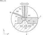
- FIG. 21 is an enlarged cross-sectional view of the main part showing the method of manufacturing the semiconductor device according to the first embodiment of the present disclosure.
- FIG. 22 is a main part plan view showing the method of manufacturing the semiconductor device according to the first embodiment of the present disclosure; 23 is a cross-sectional view taken along line XXIII-XXIII of FIG. 22.
- FIG. FIG. 24 is an enlarged cross-sectional view of main parts showing a modification of the method for manufacturing the semiconductor device according to the first embodiment of the present disclosure.
- FIG. 25 is an enlarged bottom view of main parts showing a modification of the semiconductor device according to the first embodiment of the present disclosure.
- FIG. 26 is an enlarged bottom view of a main part showing a modification of the semiconductor device according to the first embodiment of the present disclosure
- FIG. 27 is an enlarged bottom view of a main part showing a modification of the semiconductor device according to the first embodiment of the present disclosure
- FIG. 28 is an enlarged cross-sectional view of a main part showing the manufacturing method of the modification of the semiconductor device according to the first embodiment of the present disclosure
- FIG. 29 is an enlarged bottom view of a main part showing a modification of the semiconductor device according to the first embodiment of the present disclosure
- FIG. 30 is an enlarged cross-sectional view of main parts of a modification of the semiconductor device according to the first embodiment of the present disclosure.
- FIG. 31 is an enlarged cross-sectional view of main parts showing a modification of the semiconductor device according to the first embodiment of the present disclosure.
- FIG. 32 is a cross-sectional view showing a semiconductor device according to a second embodiment of the present disclosure; 33A and 33B are cross-sectional views showing a method for manufacturing a semiconductor device according to the second embodiment of the present disclosure.
- a semiconductor device A1 of this embodiment includes a first lead 1, a plurality of second leads 2, a plurality of third leads 3, a semiconductor element 4, a plurality of first wires 51, a plurality of second wires 52, and a sealing resin 8. It has The shape and size of the semiconductor device A1 are not particularly limited. An example of the size of the semiconductor device A1 is about 4 mm to 7 mm in the x direction, about 4 mm to 8 mm in the y direction, and about 0.7 mm to 2.0 mm in the z direction. be.
- FIG. 1 is a plan view showing the semiconductor device A1.
- FIG. 2 is a fragmentary plan view showing the semiconductor device A1.
- FIG. 3 is a bottom view of essential parts showing the semiconductor device A1.
- FIG. 4 is a front view showing the semiconductor device A1.
- FIG. 5 is a side view showing the semiconductor device A1.
- 6 is a cross-sectional view taken along line VI-VI of FIG. 3.
- FIG. 7 is a cross-sectional view along line VII-VII of FIG.
- FIG. 8 is an enlarged cross-sectional view of a main part showing the semiconductor device A1.
- FIG. 9 is an enlarged bottom view of essential parts showing the semiconductor device A1.
- FIG. 10 is an enlarged cross-sectional view of a main part showing the semiconductor device A1.
- FIG. 10 is an enlarged cross-sectional view of a main part showing the semiconductor device A1.
- FIG. 11 is an enlarged bottom view of essential parts showing the semiconductor device A1. 2 and 3, the sealing resin 8 is indicated by imaginary lines for convenience of understanding, and the covering portion 7 is omitted in FIG. 3 for convenience of understanding. 9 shows only part of the second lead 2, and FIG. 11 shows only part of the third lead 3. As shown in FIG.
- the first lead 1 is a member that supports the semiconductor element 4 and constitutes a conduction path to the semiconductor element 4 .
- the material of first lead 1 is not particularly limited, and is made of, for example, metals represented by Cu, Ni, Fe, etc., and alloys thereof.
- the first lead 1 may be formed with a plated layer made of a metal represented by Ag, Ni, Pd, Au, etc., at an appropriate position.
- the thickness of first lead 1 is not particularly limited, and is, for example, about 0.12 mm to 0.2 mm.
- the first lead 1 of this embodiment has a die pad portion 11 and two extension portions 12 .
- the die pad portion 11 is a portion that supports the semiconductor element 4 .
- the shape of the die pad portion 11 is not particularly limited, and is rectangular when viewed in the z direction in this embodiment.
- the die pad portion 11 has a die pad main surface 111 and a die pad back surface 112 .
- the die pad main surface 111 is a surface facing the z direction.
- the die pad back surface 112 is a surface facing away from the die pad main surface 111 in the thickness direction. In the illustrated example, die pad main surface 111 and die pad back surface 112 are planar.
- the two extending portions 12 are portions extending from the die pad portion 11 to opposite sides in the x direction.
- the extending portion 12 includes a portion extending from the die pad portion 11 along the x direction, a portion extending obliquely in the z direction toward the die pad main surface 111 with respect to the portion, and a portion extending from the portion extending in the z direction. It has a portion extending along the x-direction, and has a bent shape as a whole.
- the plurality of second leads 2 are separated from the first leads 1 and constitute a conductive path to the semiconductor element 4 .
- the plurality of second leads 2 constitute conduction paths for currents switched by the semiconductor element 4 .
- a plurality of second leads 2 are arranged on one side of the first leads 1 in the y direction. Also, the plurality of second leads 2 are arranged apart from each other in the x direction.
- the material of the second lead 2 is not particularly limited, and is made of, for example, metals represented by Cu, Ni, Fe, etc., and alloys thereof. Moreover, the second lead 2 may be formed with a plated layer made of a metal represented by Ag, Ni, Pd, Au, etc., at an appropriate position. The thickness of second lead 2 is not particularly limited, and is, for example, about 0.12 mm to 0.2 mm.
- the second lead 2 of this embodiment has a bonding pad portion 21 , a terminal portion 22 and a connecting portion 23 .
- the bonding pad portion 21 is a portion to which the first wire 51 is connected.
- the bonding pad portion 21 is located on the side (upper side in the figure) on which the die pad main surface 111 faces the die pad portion 11 in the z direction.
- the bonding pad portion 21 has a bonding pad main surface 211 , a bonding pad back surface 212 and a first portion 213 .
- the bonding pad main surface 211 faces the same side as the die pad main surface 111 in the z direction. It is preferable that all or part of the bonding pad main surface 211 is provided with the plating layer described above.
- the bonding pad main surface 211 is located on the side (upper side in the figure) facing the die pad main surface 111 with respect to the die pad main surface 111 in the z direction.
- the bonding pad back surface 212 is a surface facing the opposite side of the bonding pad main surface 211 in the z direction.
- the bonding pad back surface 212 is located on the side (upper side in the figure) on which the die pad main surface 111 faces the die pad back surface 112 in the z direction.
- the first portion 213 is connected to the bonding pad rear surface 212 and is surrounded by the bonding pad rear surface 212 when viewed in the z direction.
- the first portion 213 includes a portion located at a different position from the bonding pad back surface 212 in the z-direction.
- a specific configuration of the first part 213 is not particularly limited.
- the first portion 213 of this embodiment is a concave portion having an opening edge 2130 on the bonding pad rear surface 212 and recessed toward the bonding pad main surface 211 side in the z direction.
- a specific configuration of the first portion 213 configured by the concave portion is not particularly limited.
- the first portion 213 has an open edge 2130 , a first surface 2131 and a bottom surface 2135 .
- the opening edge 2130 is the edge that contacts the bonding pad back surface 212 .
- the shape of the opening edge 2130 is not particularly limited, and various shapes such as circular, elliptical, and polygonal may be adopted as appropriate. In the illustrated example, the opening edge 2130 is circular.
- the first surface 2131 is a surface that is inclined away from the bonding pad rear surface 212 as viewed in the z direction as it separates from the bonding pad rear surface 212 toward the bonding pad main surface 211 in the z direction.
- the shape and size of the first surface 2131 are not particularly limited.
- the angle ⁇ 1 is the angle formed between the first surface 2131 and the xy plane, which is a plane perpendicular to the z direction.
- the angle ⁇ 1 is preferably 25° or more and 50° or less, for example.
- the first surface 2131 has an annular shape when viewed in the z direction, and more specifically has an annular shape. Since the first surface 2131 is such an inclined surface, the portion of the recessed first portion 213 other than the opening edge 2130 is located inside the opening edge 2130 when viewed in the z direction.
- the bottom surface 2135 is the surface of the first portion 213 that is closest to the bonding pad main surface 211 in the z direction.
- the specific shape and size of the bottom surface 2135 are not particularly limited, and various shapes such as circular, elliptical, and polygonal are appropriately employed. In the illustrated example, the bottom surface 2135 is circular.
- the depth in the z direction of the first portion 213 is 1/4 or more and 1/2 or less of the thickness of the bonding pad portion 21 (second lead 2).
- the diameter of the opening edge 2130 is 0.5 times or more the thickness of the bonding pad portion 21 (second lead 2). 5 times or less.
- the terminal portion 22 is a belt-like portion extending in the y direction outside the sealing resin 8 .
- the terminal portion 22 is arranged at a position overlapping the die pad portion 11 when viewed in the y direction.
- the connecting portion 23 is a portion that connects the bonding pad portion 21 and the terminal portion 22 .
- the connecting portion 23 has a bent shape when viewed in the x direction.
- the connecting portion 23 includes a portion covered with the sealing resin 8 and a portion exposed from the sealing resin 8 .
- the plurality of third leads 3 are separated from the first leads 1 and constitute a conductive path to the semiconductor element 4 .
- the plurality of third leads 3 constitute conduction paths for control signal currents for controlling the semiconductor element 4 .
- a plurality of third leads 3 are arranged on the other side in the y direction with respect to the first leads 1 . Also, the plurality of third leads 3 are arranged apart from each other in the x direction.
- the material of the third lead 3 is not particularly limited, and is made of, for example, metals represented by Cu, Ni, Fe, etc., and alloys thereof. Also, the third lead 3 may be formed with a plated layer made of a metal represented by Ag, Ni, Pd, Au, etc., at an appropriate position. The thickness of the third lead 3 is not particularly limited, and is, for example, approximately 0.12 mm to 0.2 mm.
- the third lead 3 of this embodiment has a bonding pad portion 31 , a terminal portion 32 and a connecting portion 33 .
- the bonding pad portion 31 is a portion to which the second wire 52 is connected.
- the bonding pad portion 31 is located on the side (upper side in the figure) on which the die pad main surface 111 faces the die pad portion 11 in the z direction.
- the bonding pad portion 31 has a bonding pad main surface 311 , a bonding pad back surface 312 and a third portion 313 .
- the bonding pad main surface 311 faces the same side as the die pad main surface 111 in the z direction. It is preferable that all or part of the bonding pad main surface 311 is provided with the plating layer described above.
- the bonding pad main surface 311 is located on the side (upper side in the figure) facing the die pad main surface 111 with respect to the die pad main surface 111 in the z direction.
- the bonding pad back surface 312 is a surface facing the opposite side of the bonding pad main surface 311 in the z direction.
- the bonding pad back surface 312 is located on the side (upper side in the figure) on which the die pad main surface 111 faces the die pad back surface 112 in the z direction.
- the third portion 313 is connected to the bonding pad rear surface 312 and is surrounded by the bonding pad rear surface 312 when viewed in the z direction.
- the third portion 313 includes a portion located at a different position from the bonding pad back surface 312 in the z-direction.
- a specific configuration of the third part 313 is not particularly limited.
- the third portion 313 of this embodiment is a concave portion having an opening edge 3130 on the bonding pad rear surface 312 and recessed toward the bonding pad main surface 311 side in the z direction.
- the specific configuration of the third portion 313 configured by recesses is not particularly limited.
- the third portion 313 has an open edge 3130 , a first surface 3131 and a bottom surface 3135 .
- the opening edge 3130 is the edge that contacts the bonding pad back surface 312 .
- the shape of the opening edge 3130 is not particularly limited, and various shapes such as circular, elliptical, and polygonal may be adopted as appropriate. In the illustrated example, the opening edge 3130 is circular.
- the first surface 3131 is a surface that is inclined away from the bonding pad rear surface 312 as viewed in the z direction as it separates from the bonding pad rear surface 312 toward the bonding pad main surface 311 in the z direction.
- the shape and size of the first surface 3131 are not particularly limited.
- the angle ⁇ 2 is the angle between the first surface 3131 and the xy plane, which is a plane perpendicular to the z direction.
- the angle ⁇ 2 is preferably, for example, 25° or more and 50° or less.
- the first surface 3131 has an annular shape when viewed in the z-direction, and more specifically has an annular shape. Since the first surface 3131 is such an inclined surface, the portion other than the opening edge 3130 of the recessed third portion 313 is located inside the opening edge 3130 when viewed in the z direction.
- the bottom surface 3135 is the surface of the third portion 313 that is closest to the bonding pad main surface 311 in the z direction.
- the specific shape and size of the bottom surface 3135 are not particularly limited, and various shapes such as circular, elliptical, and polygonal may be adopted as appropriate. In the illustrated example, the bottom surface 3135 is circular.
- the depth in the z direction of the third portion 313 is 1/4 or more and 1/2 or less of the thickness of the bonding pad portion 31 (third lead 3).
- the diameter of the opening edge 3130 is 0.5 times or more the thickness of the bonding pad portion 31 (third lead 3). 5 times or less.
- the terminal portion 32 is a belt-like portion extending in the y direction outside the sealing resin 8 .
- the terminal portion 32 is arranged at a position overlapping the die pad portion 11 when viewed in the y direction.
- the connecting portion 33 is a portion that connects the bonding pad portion 31 and the terminal portion 32 .
- the connecting portion 33 has a bent shape when viewed in the x direction.
- the connecting portion 33 includes a portion covered with the sealing resin 8 and a portion exposed from the sealing resin 8 .
- the semiconductor element 4 is an element that exhibits the electrical functions of the semiconductor device A1.
- the specific configuration of the semiconductor element 4 is not particularly limited, and various types of semiconductor elements can be selected as appropriate.
- the semiconductor element 4 performs a switching function.
- the semiconductor element 4 has an element body 40 , first electrodes 401 , second electrodes 402 and a plurality of third electrodes 403 .
- the semiconductor device 4 also has a control section 48 .
- the semiconductor element 4 has a portion that constitutes a transistor that performs a switching function, and a portion that controls, monitors, protects, etc. the transistor.
- the specific configuration of the semiconductor element 4 is not particularly limited.
- the semiconductor element 4 may have a functional layer 408 or the like as a portion that constitutes a transistor, and may have a configuration without the control section 48 .
- the number and presence/absence of the second electrodes 402 and the third electrodes 403 are appropriately selected.
- other semiconductor elements may be mounted on the die pad portion 11 in addition to the semiconductor element 4 .
- the functions of the semiconductor elements other than the semiconductor element 4 are not particularly limited.
- the element main body 40 has an element main surface 40a and an element back surface 40b.
- the element main surface 40a faces the same side as the die pad main surface 111 in the z direction.
- the element back surface 40b is a surface that faces the side opposite to the element main surface 40a in the z direction.
- the material of the element main body 40 is not particularly limited. Examples of materials for the element body 40 include semiconductor materials such as Si, SiC, and GaN.
- the element body 40 has a functional layer 408, for example, as shown in FIG.
- the functional layer 408 has a transistor structure typified by, for example, a MOSFET (Metal Oxide Semiconductor Field Effect Transistor), a MISFET (Metal Insulator Semiconductor Field Effect Transistor), and the like.
- the functional layer 408 is arranged side by side with the control unit 48 in the y direction when viewed in the z direction.
- the specific arrangement of the functional layer 408 and the controller 48 is not particularly limited.
- the first electrode 401 is arranged on the element main surface 40 a of the element body 40 .
- the shape, size and position of the first electrode 401 are not particularly limited.
- the first electrode 401 is arranged on a portion of the element main surface 40a on the side of the plurality of second leads 2 in the y direction.
- the first electrode 401 overlaps the functional layer 408 when viewed in the z direction.
- the first electrode 401 is separated from the control section 48 when viewed in the z direction.
- the first electrode 401 is the source electrode.
- the material of the first electrode 401 is not particularly limited, and examples thereof include metals represented by Al (aluminum), Al—Si, Cu (copper), and alloys containing these.
- the first electrode 401 may have a structure in which layers made of a plurality of materials selected from these metals are laminated.
- the second electrode 402 is arranged on the element back surface 40 b of the element body 40 .
- the second electrode 402 overlaps the functional layer 408 and the control section 48 when viewed in the z-direction, and covers the entire back surface 40b of the element in this embodiment.
- the second electrode 402 is the drain electrode.
- the material of the second electrode 402 is not particularly limited, and examples thereof include metals represented by Al, Al--Si, Cu, etc., and alloys containing these.
- the second electrode 402 may have a structure in which layers made of a plurality of materials selected from these metals are laminated.
- Control unit 48 includes, for example, a current sensor circuit, a temperature sensor circuit, an overcurrent protection circuit, an overheating protection circuit, a low voltage malfunction prevention circuit, and the like.
- the plurality of third electrodes 403 are arranged on the element main surface 40a.
- the plurality of third electrodes 403 are arranged on the portion of the element main surface 40a on the side of the plurality of third leads 3 in the y direction.
- the plurality of third electrodes 403 overlap the control section 48 when viewed in the z direction.
- the plurality of third electrodes 403 are mainly electrically connected to the controller 48 .
- the number of the multiple third electrodes 403 is not particularly limited. Also, the number of third electrodes 403 may be one.
- the semiconductor element 4 has four third electrodes 403 .
- the plurality of first wires 51 electrically connect the first electrodes 401 of the semiconductor element 4 and the plurality of second leads 2 .
- the material of first wire 51 is not particularly limited, and is made of metal represented by Au, Cu, Al, or the like, for example.
- the first wire 51 of this embodiment has a bonding portion 511 , a bonding portion 512 and a loop portion 513 .
- a specific configuration of the first wire 51 is not particularly limited.
- first wire 51 is made of a material containing Cu, and is formed by a capillary, for example. In this embodiment, a current switched by the semiconductor element 4 flows through the plurality of first wires 51 .
- the bonding portion 511 is bonded to the first electrode 401 of the semiconductor element 4 and arranged at a position overlapping the first electrode 401 when viewed in the z direction.
- the bonding portion 511 is a so-called first bonding portion.
- the arrangement of the bonding portion 511 is not particularly limited.
- the bonding portions 511 of the plurality of first wires 51 are distributed over substantially the entire area of the first electrode 401 .
- the bonding portions 511 of the plurality of first wires 51 may be arranged in one or more rows along the outer peripheral edge of the first electrode 401, for example.
- the bonding portion 512 is a portion that is bonded to the bonding pad main surface 211 of the bonding pad portion 21 of the second lead 2 .
- the bonding portion 512 is a so-called second bonding portion.
- a plurality of bonding portions 512 are arranged on one bonding pad portion 21 . Any one of the plurality of bonding portions 512 bonded to one bonding pad portion 21 and the first portion 213 preferably partially overlap each other when viewed in the z direction. However, the plurality of bonding portions 512 bonded to one bonding pad portion 21 and the first portion 213 may be configured so as not to overlap when viewed in the z direction.
- the loop portion 513 is connected to the bonding portion 511 and the bonding portion 512 and has a curved shape.
- the plurality of second wires 52 electrically connect the third electrodes 403 of the semiconductor element 4 and the plurality of third leads 3 .
- the material of the second wire 52 is not particularly limited, and is made of metal represented by Au, Cu, Al, or the like, for example.
- the second wire 52 has a bonding portion 521 , a bonding portion 522 and a loop portion 523 .
- a specific configuration of the second wire 52 is not particularly limited.
- the second wire 52 is formed by a capillary, for example.
- a control signal current for controlling the semiconductor element 4 flows through the plurality of second wires 52 .
- the bonding portion 521 is joined to the second electrode 402 of the semiconductor element 4 .
- the bonding portion 521 is a so-called first bonding portion.
- the bonding portion 522 is a portion that is bonded to the bonding pad main surface 311 of the bonding pad portion 31 of the third lead 3 .
- the bonding portion 522 is a so-called second bonding portion.
- one bonding portion 522 is arranged on one bonding pad portion 31 . It is preferable that the bonding portion 522 and the third portion 313 overlap each other at least partially when viewed in the z direction. Alternatively, the bonding portion 522 and the third portion 313 may be configured so that they do not overlap when viewed in the z direction.
- the loop portion 523 is connected to the bonding portion 521 and the bonding portion 522 and has a curved shape.
- the sealing resin 8 covers the first lead 1 , the plurality of second leads 2 , the plurality of third leads 3 , the semiconductor element 4 , the plurality of first wires 51 , the plurality of second wires 52 and the covering portion 7 . .
- a portion of the first lead 1, a portion of each second lead 2, and a portion of each third lead are exposed from the sealing resin 8.
- the encapsulating resin 8 is made of an insulating resin, and includes, for example, an epoxy resin mixed with a filler. Further, in this embodiment, part of the sealing resin 8 fills the first portion 213 of the second lead 2 and the third portion 313 of the third lead 3 .
- the shape of the sealing resin 8 is not particularly limited.
- the sealing resin 8 has a resin main surface 81 , a resin back surface 82 , two first resin side surfaces 83 and two second resin side surfaces 84 .
- the resin main surface 81 faces the same side as the die pad main surface 111 in the z direction, and is flat, for example.
- the resin back surface 82 is a surface facing the opposite side of the resin main surface 81 in the z-direction, and is, for example, a flat surface.
- the two first resin side surfaces 83 are located between the resin main surface 81 and the resin back surface 82 in the z direction, and face opposite sides in the x direction.
- the two second resin side surfaces 84 are positioned between the resin main surface 81 and the resin back surface 82 in the z direction, and face opposite sides in the y direction.
- FIG. 12 An example of a method for manufacturing the semiconductor device A1 will be described below with reference to FIGS. 12 to 22.
- FIG. 12 An example of a method for manufacturing the semiconductor device A1 will be described below with reference to FIGS. 12 to 22.
- a first lead 1, a plurality of second leads 2 and a plurality of third leads 3 are prepared.
- the first lead 1, the plurality of second leads 2, and the plurality of third leads 3 may be individually separated, or a lead frame having a frame (not shown) connecting them may be used. may be used.
- a lead frame is used, after the steps described below are completed, the lead frame is cut at appropriate locations to obtain the first lead 1, the plurality of second leads 2 and the plurality of third leads 3 which are separated into pieces. can get.
- a first lead 1 , a plurality of second leads 2 and a third lead 3 are supported by a support 9 .
- the support 9 is a member made of metal or the like, for example.
- the specific configuration of the support 9 is not particularly limited, and has a base surface 90 , a support surface 91 , a second portion 92 , a support surface 93 and a fourth portion 94 in this embodiment.
- the base surface 90 is a surface that occupies most of the area of the support 9, and faces the upper side in the figure (the side to which the die pad main surface 111 faces) in the z direction.
- the base surface 90 supports the die pad portion 11, the terminal portion 22, the terminal portion 32, and the like.
- the support surface 91 faces the upper side in the figure (the side to which the die pad main surface 111 faces) in the z direction, and is located above the base surface 90 in the figure (the side to which the die pad main surface 111 faces).
- the support surface 91 supports the bonding pad portion 21 and is in contact with the bonding pad rear surface 212 .
- the second part 92 is a part that engages with the first part 213 of the bonding pad part 21 of the second lead 2 .
- the specific configuration of the second portion 92 is not particularly limited, and in the illustrated example, it is a truncated conical projection corresponding to the configuration of the first portion 213 described above.
- This second part 92 has a first surface 921 and a top surface 925 .
- the first surface 921 is a surface that faces the first surface 2131 and can come into contact therewith. Like the first surface 2131, the first surface 921 is inclined by an angle ⁇ 1 (or 180° ⁇ angle ⁇ 1) with respect to the xy plane. Also, the first surface 921 has an annular shape when viewed in the z-direction, like the first surface 2131 .
- the top surface 925 is a tip surface of the second portion 92 that is a convex portion, and is a surface that faces the bottom surface 2135 and can come into contact therewith.
- the top surface 925 is circular, corresponding to the bottom surface 2135 .
- the support surface 93 faces the upper side in the drawing (the side to which the die pad main surface 111 faces) in the z direction, and is located above the base surface 90 in the drawing (the side to which the die pad main surface 111 faces).
- the support surface 93 supports the bonding pad portion 31 and is in contact with the bonding pad rear surface 312 .
- the fourth portion 94 is a portion that engages with the third portion 313 of the bonding pad portion 31 of the third lead 3 .
- the specific configuration of the fourth portion 94 is not particularly limited, and in the illustrated example, it is a truncated conical projection corresponding to the configuration of the third portion 313 described above.
- This fourth portion 94 has a first surface 941 and a top surface 945 .
- the first surface 941 is a surface that faces the first surface 3131 and can come into contact therewith. Like the first surface 3131, the first surface 941 is inclined by an angle ⁇ 2 (or 180° ⁇ angle ⁇ 2) with respect to the xy plane. Also, the first surface 941 has an annular shape when viewed in the z-direction, like the first surface 3131 .
- the top surface 945 is the tip surface of the fourth portion 94 that is a convex portion, and is a surface that faces the bottom surface 3135 and can come into contact therewith.
- the top surface 945 is circular, corresponding to the bottom surface 3135 .
- the semiconductor element 4 is mounted on the first lead 1. Then, as shown in FIGS. Specifically, the second electrode 402 of the semiconductor element 4 and the die pad main surface 111 of the die pad portion 11 of the first lead 1 are bonded using a bonding paste as a material of the bonding material 49 .
- the plurality of first wires 51 and the plurality of second wires 52 are bonded.
- the order of bonding the plurality of first wires 51 and the plurality of second wires 52 is not particularly limited.
- the plurality of second wires 52 may be bonded after all the first wires 51 are bonded, or the plurality of first wires 51 may be bonded after all the second wires 52 are bonded.
- the first wires 51 and the second wires 52 may be alternately bonded.
- first, bonding of the first wire 51 will be described.
- the bonding of the second wire 52 is performed in a manner similar to the bonding of the first wire 51 .
- first bonding is performed on the first electrode 401 using a capillary Cp.
- the capillary Cp holds the wire material 510 so that it can move back and forth.
- a predetermined amount of wire material 510 is protruded from the capillary Cp and melted.
- the molten wire material 510 is attached to the first electrode 401 .
- a bonding portion 511 is formed.
- the capillary Cp is brought closer to the bonding pad portion 21 of the second lead 2 along a predetermined path. Thereby, the loop portion 513 shown in FIG. 19 is formed. Then, the wire material 510 is pressed against the bonding pad main surface 211 of the bonding pad portion 21 by the capillary Cp. At this time, it is preferable to press the wire material 510 to a position overlapping the first portion 213 when viewed in the z direction. However, the wire material 510 may be pressed to a position that does not overlap the first portion 213 . Then, as shown in FIG. 20, force and vibration are applied to the wire material 510 from the capillary Cp.
- This vibration is, for example, ultrasonic vibration.
- wire material 510 is bonded to bonding pad main surface 211 .
- the capillary Cp is separated upward in the z-direction from the bonding pad portion 21 in a state in which the wire material 510 is not extended.
- the first wire 51 having the bonding portion 511, the bonding portion 512 and the loop portion 513 is formed.
- the formation of the second wire 52 is performed using a capillary Cp in the same manner as the first wire 51 .
- bonding portion 522 is formed on bonding pad main surface 311 of bonding pad portion 31 of third lead 3, as shown in FIG.
- the bonding portion 522 is formed by pressing the wire material 510 against the bonding pad main surface 311 of the bonding pad portion 31 by the capillary Cp, similarly to the formation of the bonding portion 512 .
- the wire material 510 may be pressed to a position overlapping the third portion 313 .
- a plurality of first wires 51 and a plurality of second wires 52 are formed as shown in FIGS.
- the first lead 1 , the plurality of second leads 2 , the plurality of third leads 3 , the semiconductor element 4 , the plurality of first wires 51 and the plurality of second wires 52 are separated from the support 9 .
- the sealing resin 8 is formed by, for example, mold molding. Thereby, the semiconductor device A1 described above is obtained.
- the bonding pad section 21 has the first section 213 .
- the first portion 213 engages the second portion 92 of the support 9, as shown in FIGS.
- the bonding pad portion 21 is unintentionally moved along the xy plane. It is possible to suppress misalignment. Therefore, according to this embodiment, the first wire 51 can be bonded more reliably.
- the first portion 213 overlaps the bonding portion 512 when viewed in the z direction. As a result, the force and vibration when forming the bonding portion 512 can be more reliably received by the engaging structure between the bonding portion 512 and the second portion 92 .
- the bonding portion 512 is the second bonding portion, a larger force and vibration are likely to be applied to the bonding pad portion 21 when the bonding portion 512 is formed.
- the bonding portion 512 which is the second bonding portion, can be formed more appropriately.
- the first part 213 is configured by a recess. This makes it possible to prevent the first part 213 from unintentionally interfering with other members or the like in the method of manufacturing the semiconductor device A1.
- the first surface 2131 of the first portion 213 is an inclined surface that is inclined away from the bonding pad rear surface 212 when viewed in the z direction as the distance from the bonding pad rear surface 212 increases in the z direction.
- the bonding pad portion 21 can be smoothly detached from the support 9 after the bonding of the first wire 51 is completed. can be done. Further, when the second lead 2 is supported by the support 9, even if the first portion 213 is arranged at a position slightly deviated from the second portion 92, the bonding pad portion 21 is positioned downward in the z direction.
- the angle ⁇ 1 is preferably 25° or more and 50° or less in order to more appropriately obtain the effect of the first surface 2131 being an inclined surface.
- the depth of the first portion 213 in the z-direction is 1/4 or more and 1/2 or less of the thickness of the second lead 2 (bonding pad portion 21) separates the first portion 213 and the second portion 92 from each other. This is preferable for avoiding an unreasonable decrease in rigidity of the bonding pad portion 21 while ensuring proper engagement.
- FIG. 24 shows a first modification of the method for manufacturing the semiconductor device A1.
- the first surface 2131 of the first portion 213 of the bonding pad portion 21 and the first surface 921 of the second portion 92 are in contact with each other, and the bottom surface 2135 of the first portion 213 and the second portion 92 are separated from each other by a gap. That is, in this modification, the height of the second portion 92 in the z direction is smaller than the depth of the first portion 213 in the z direction.
- the first wire 51 can be bonded more reliably.
- the specific configuration of the first portion 213 and the second portion 92 and the state of contact between the first portion 213 and the second portion 92 are not particularly limited. Also, the configurations of the first portion 213 and the second portion 92 to be described after the modification can be similarly applied to the third portion 313 and the fourth portion 94 .
- the height of the second portion 92 is smaller than the depth of the first portion 213, the back surface 212 of the bonding pad and the support surface 91 can be brought into contact with each other more reliably. Further, by making the size of the opening edge 2130 smaller than the size of the boundary between the second portion 92 and the support surface 91, the first surface 2131 and the first surface 921 can be brought into contact with each other more reliably. can be done. Thereby, in bonding the first wire 51 using the capillary Cp, it is possible to further suppress the bonding pad portion 21 from being shifted in the xy plane.
- FIG. 25 shows the first part 213 according to the second modified example of the semiconductor device A1.
- the first portion 213 of this modification has an opening edge 2130 , a first surface 2131 , a second surface 2132 , a third surface 2133 , a fourth surface 2134 and a bottom surface 2135 .
- the opening edge 2130 has a rectangular shape when viewed in the z direction.
- the first surface 2131, the second surface 2132, the third surface 2133, and the fourth surface 2134 are all inclined at an angle ⁇ 1, for example, with respect to the xy plane, like the first surface 2131 described above.
- the first surface 2131, the second surface 2132, the third surface 2133, and the fourth surface 2134 are arranged at different positions when viewed in the z direction.
- the first surface 2131, the second surface 2132, the third surface 2133, and the fourth surface 2134 are arranged to form a rectangular ring surrounding the bottom surface 2135 when viewed in the z direction.
- the first wire 51 can be bonded more reliably.
- the specific configuration of the first part 213 is not particularly limited.
- the shape and size of the second portion 92 that can be engaged may be appropriately adopted according to the shape and size of the first portion 213 .
- FIG. 26 shows the first part 213 according to the third modified example of the semiconductor device A1.
- the first part 213 of this modification has an open edge 2130 , a first surface 2131 , a second surface 2132 , a third surface 2133 and a bottom surface 2135 .
- the opening edge 2130 has a triangular shape when viewed in the z direction.
- the first surface 2131, the second surface 2132, and the third surface 2133 are all inclined at an angle ⁇ 1, for example, with respect to the xy plane, similarly to the first surface 2131 described above.
- the first surface 2131, the second surface 2132 and the third surface 2133 are arranged at different positions when viewed in the z direction.
- the first surface 2131, the second surface 2132 and the third surface 2133 are arranged to form a triangular ring surrounding the bottom surface 2135 when viewed in the z direction.
- the first wire 51 can be bonded more reliably.
- the specific configuration of the first part 213 is not particularly limited.
- the opening edge 2130 of the first portion 213 may be polygonal, for example.
- the first portion 213 of this variation has an open edge 2130 and a first surface 2131 and does not have the bottom surface 2135 described above.
- the first surface 2131 of this modified example has a conical shape.
- a truncated cone-shaped second portion 92 may be adopted.
- the first wire 51 can be bonded more reliably.
- the first portion 213 may have a shape that does not have the bottom surface 2135 .
- FIG. 29 shows the first part 213 according to the fifth modified example of the semiconductor device A1.
- the first portion 213 of this modified example has a first surface 2131, a second surface 2132, a third surface 2133 and a fourth surface 2134, and does not have a bottom surface 2135 as in the fourth modified example.
- the first part 213 has a pyramidal shape. Also according to this modification, the first wire 51 can be bonded more reliably.
- the first portion 213 of this modification has an open edge 2130 and a first surface 2131 .
- the first surface 2131 is entirely concave.
- the first portion 213 has a hemispherical shape (or a substantially hemispherical shape) as a whole.
- the angle ⁇ 1 of the portion of the first surface 2131 that is connected to the opening edge 2130 is preferably sufficiently smaller than 90°.
- the second part 92 may have a hemispherical shape (or a substantially hemispherical shape).
- the second portion 92 may have a hemispherical shape with a flat top surface 925 (see FIG. 14).
- the first wire 51 can be bonded more reliably.
- the first surface 2131 may be a concave curved surface or a convex curved surface.
- the semiconductor device A2 of this embodiment differs from the semiconductor device A1 described above in the configuration of the first portion 213 and the third portion 313 .
- the first portion 213 is configured by a convex portion projecting from the bonding pad back surface 212 toward the bonding pad back surface 212 in the z direction. Also in this embodiment, only one first portion 213 is provided in one bonding pad portion 21 . The first portion 213 is connected to the bonding pad rear surface 212 and is surrounded by the bonding pad rear surface 212 when viewed in the z direction. The first portion 213 of the present embodiment also has a configuration including a portion located at a different position from the bonding pad back surface 212 in the z direction.
- the third portion 313 is configured by a convex portion protruding from the bonding pad back surface 312 toward the bonding pad back surface 312 in the z direction. Also in this embodiment, only one third portion 313 is provided in one bonding pad portion 31 . Also, the third portion 313 is connected to the bonding pad rear surface 312 and is surrounded by the bonding pad rear surface 312 when viewed in the z direction. The third portion 313 of the present embodiment also has a configuration including a portion located at a different position from the bonding pad back surface 312 in the z direction.
- the second part 92 and the fourth part 94 are configured by concave portions that can be engaged with the first part 213 and the third part 313 are used.
- the engagement of the first part 213 and the second part 92 and the engagement of the third part 313 and the fourth part 94 are realized, and the first wire 51 and the second wire 51 are connected to each other. Bonding of wires 52 may be performed.
- the first wire 51 can be bonded more reliably.
- the first portion 213 and the third portion 313 may be configured by concave portions or may be configured by convex portions.
- the semiconductor device and the method of manufacturing the semiconductor device according to the present disclosure are not limited to the above-described embodiments.
- the specific configuration of the semiconductor device and the method of manufacturing the semiconductor device according to the present disclosure can be modified in various ways.
- the present disclosure includes embodiments described in the appendices below.
- Appendix 1 a semiconductor element having a device body containing a semiconductor and a first electrode disposed on the device body; a first lead on which the semiconductor element is mounted; a second lead; a first wire that electrically connects the semiconductor element and the second lead;
- the first lead includes a die pad portion having a die pad main surface and a die pad back surface facing opposite to each other in the thickness direction;
- the semiconductor element is mounted on the main surface of the die pad
- the second lead includes a bonding pad portion having a bonding pad main surface facing the same side as the die pad main surface in the thickness direction and a bonding pad back surface facing the side opposite to the bonding pad main surface;
- the back surface of the bonding pad is arranged on the side where the main surface of the die pad is located with respect to the back surface of the die pad in the thickness direction,
- the first wire is bonded to the first electrode and the main surface of the bonding pad,
- the bonding pad portion has only one first portion, and the first portion is connected to the bonding
- Appendix 2. the first wire has a bonding portion bonded to the main surface of the bonding pad, The semiconductor device according to appendix 1, wherein the bonding portion and the first portion at least partially overlap with each other when viewed in the thickness direction. Appendix 3.
- Appendix 4. The semiconductor device according to any one of appendices 1 to 3, wherein the first part is a recess having an opening edge on the back surface of the bonding pad.
- Appendix 5. The semiconductor device according to appendix 4, wherein a portion of the recess other than the opening edge is located inside the opening edge when viewed in the thickness direction. Appendix 6. 6.
- the semiconductor device according to appendix 5 wherein the recess includes a first surface that is inclined away from the back surface of the bonding pad when viewed in the thickness direction as it moves away from the back surface of the bonding pad in the thickness direction.
- Appendix 7. The semiconductor device according to appendix 6, wherein a first angle formed between the first surface and a plane orthogonal to the thickness direction is 25° or more and 50° or less.
- Appendix 8. 8.
- the recess is inclined away from the back surface of the bonding pad when viewed in the thickness direction as the recess is separated from the back surface of the bonding pad in the thickness direction, and is positioned at a different position from the first surface when viewed in the thickness direction.
- Appendix 6 or 7 comprising a second surface arranged on the .
- Appendix 10. 4 The semiconductor device according to any one of appendices 1 to 3, wherein the first part is a convex part protruding from the back surface of the bonding pad.
- Appendix 11. 11.
- the semiconductor device according to any one of appendices 1 to 10 further comprising a sealing resin that covers the semiconductor element and the first wire, and at least part of each of the first lead and the second lead.
- a first lead including a die pad portion having a die pad main surface and a die pad back surface facing opposite to each other in the thickness direction, and a bonding pad main surface and the bonding pad main surface facing the same side as the die pad main surface in the thickness direction.
- the back surface of the bonding pad is arranged on the side where the main surface of the die pad is located with respect to the back surface of the die pad in the thickness direction,
- the bonding pad portion has only one first portion, and the first portion is connected to the bonding pad back surface and surrounded by the bonding pad back surface when viewed in the thickness direction, and has the thickness including a portion arranged at a position different in direction from the back surface of
- Appendix 17. The method of manufacturing a semiconductor device according to appendix 16, wherein the first part is a recess having an opening edge on the back surface of the bonding pad. Appendix 18. 18. The method of manufacturing a semiconductor device according to appendix 17, wherein a portion of the recess other than the opening edge is located inside the opening edge when viewed in the thickness direction.
Landscapes
- Engineering & Computer Science (AREA)
- Computer Hardware Design (AREA)
- Microelectronics & Electronic Packaging (AREA)
- Power Engineering (AREA)
- Physics & Mathematics (AREA)
- Condensed Matter Physics & Semiconductors (AREA)
- General Physics & Mathematics (AREA)
- Manufacturing & Machinery (AREA)
- Geometry (AREA)
- Wire Bonding (AREA)
Abstract
半導体装置は、半導体素子と、第1リードと、第2リードと、第1ワイヤとを備える。ボンディングパッド裏面は、z方向においてダイパッド裏面に対してダイパッド主面が位置する側に配置されている。第1ワイヤは、第1電極とボンディングパッド主面とにボンディングされている。ボンディングパッド部は、ただ1つの第1部を有する。当該第1部は、ボンディングパッド裏面に繋がり且つz方向に視てボンディングパッド裏面に囲まれているとともに、z方向においてボンディングパッド裏面とは異なる位置に存在する部分を含む。
Description
本開示は、半導体装置および半導体装置の製造方法に関する。
特許文献1には、従来の半導体装置の一例が開示されている。同文献に開示された半導体装置は、第1リード、第1リードのアイランド部に搭載された半導体素子、第2リード、およびワイヤを備える。ワイヤは、半導体素子の主面電極と、第2リードのワイヤボンディングパッドとにボンディングされている。第2リードのワイヤボンディングパッドは、第1リードのアイランド部よりも、上方に位置している。
第2リードのワイヤボンディングパッドにワイヤをボンディングする際には、当該ワイヤボンディングパッドに対し、ボンディング処理において生じる力や振動が付加される。その結果、ワイヤボンディングパッド(延いては第2リード)の位置がずれてしまう等の不具合が生じうる。これは、ワイヤボンディングが適切に行われないことに繋がり、好ましくない。
本開示は、上記した事情のもとで考え出されたものであって、より確実にワイヤをボンディングすることが可能な半導体装置を提供することを一の課題とする。
本開示の第1の側面によって提供される半導体装置は、半導体を含む素子本体および前記素子本体上に配置された第1電極を有する半導体素子と、前記半導体素子が搭載された第1リードと、第2リードと、前記半導体素子と前記第2リードとを電気的に接続する第1ワイヤと、を備え、前記第1リードは、厚さ方向において互いに反対側を向くダイパッド主面およびダイパッド裏面を有するダイパッド部を含み、前記半導体素子は、前記ダイパッド主面に搭載されており、前記第2リードは、前記厚さ方向において前記ダイパッド主面と同じ側を向くボンディングパッド主面および前記ボンディングパッド主面とは反対側を向くボンディングパッド裏面を有するボンディングパッド部を含み、前記ボンディングパッド裏面は、前記厚さ方向において前記ダイパッド裏面に対して前記ダイパッド主面が位置する側に配置されており、前記第1ワイヤは、前記第1電極と前記ボンディングパッド主面とにボンディングされており、前記ボンディングパッド部は、ただ1つの第1部を有し、当該第1部は、前記ボンディングパッド裏面に繋がり且つ前記厚さ方向に視て前記ボンディングパッド裏面に囲まれているとともに、前記厚さ方向において前記ボンディングパッド裏面とは異なる位置に存在する部分を含む。
本開示の第2の側面によって提供される半導体装置の製造方法は、厚さ方向において互いに反対側を向くダイパッド主面およびダイパッド裏面を有するダイパッド部を含む第1リード、および前記厚さ方向において前記ダイパッド主面と同じ側を向くボンディングパッド主面および前記ボンディングパッド主面とは反対側を向くボンディングパッド裏面を有するボンディングパッド部を含む第2リード、を用意する工程と、前記ダイパッド主面に、半導体を含む素子本体および前記素子本体上に配置された第1電極を有する半導体素子を搭載する工程と、前記第1電極および前記ダイパッド主面に第1ワイヤを接合する工程と、を備え、前記ボンディングパッド裏面は、前記厚さ方向において前記ダイパッド裏面に対して前記ダイパッド主面が位置する側に配置されており、前記ボンディングパッド部は、ただ1つの第1部を有し、当該第1部は、前記ボンディングパッド裏面に繋がり且つ前記厚さ方向に視て前記ボンディングパッド裏面に囲まれているとともに、前記厚さ方向において前記ボンディングパッド裏面とは異なる位置に配置された部分を含み、前記第1ワイヤを接合する工程においては、前記第2リードを支持体によって支持し、前記支持体は、前記ボンディングパッド裏面に当接する支持面と、前記第2リードの前記第1部と係合する第2部と、を有する。
本開示に基づく上記構成によれば、半導体装置において、より確実にワイヤをボンディングすることができる。
本開示のその他の特徴および利点は、添付図面を参照して以下に行う詳細な説明によって、より明らかとなろう。
以下、本開示の好ましい実施の形態につき、図面を参照して具体的に説明する。
本開示における「第1」、「第2」、「第3」等の用語は、単にラベルとして用いたものであり、それらの対象物に順列を付することを意図していない。
図1~図8は、本開示の第1実施形態に係る半導体装置A1を示している。本実施形態の半導体装置A1は、第1リード1、複数の第2リード2、複数の第3リード3、半導体素子4、複数の第1ワイヤ51、複数の第2ワイヤ52および封止樹脂8を備えている。半導体装置A1の形状および大きさは、特に限定されない。半導体装置A1の大きさの一例を挙げると、x方向の大きさが4mm~7mm程度、y方向の大きさが4mm~8mm程度、z方向の大きさが、0.7mm~2.0mm程度である。
図1は、半導体装置A1を示す平面図である。図2は、半導体装置A1を示す要部平面図である。図3は、半導体装置A1を示す要部底面図である。図4は、半導体装置A1を示す正面図である。図5は、半導体装置A1を示す側面図である。図6は、図3のVI-VI線に沿う断面図である。図7は、図3のVII-VII線に沿う断面図である。図8は、半導体装置A1を示す要部拡大断面図である。図9は、半導体装置A1を示す要部拡大底面図である。図10は、半導体装置A1を示す要部拡大断面図である。図11は、半導体装置A1を示す要部拡大底面図である。なお、図2および図3においては、理解の便宜上、封止樹脂8を想像線で示しており、図3においては、理解の便宜上、被覆部7を省略している。また、図9は、第2リード2の一部のみを示しており、図11は、第3リード3の一部のみを示している。
第1リード1は、半導体素子4を支持し、且つ半導体素子4への導通経路を構成する部材である。第1リード1の材質は特に限定されず、たとえばCu、Ni、Fe等に代表される金属およびこれらの合金からなる。また、第1リード1は、Ag、Ni、Pd、Au等に代表される金属からなるめっき層を、適所に形成されていてもよい。第1リード1の厚さは特に限定されず、たとえば0.12mm~0.2mm程度である。
本実施形態の第1リード1は、ダイパッド部11および2つの延出部12を有する。
ダイパッド部11は、半導体素子4を支持する部位である。ダイパッド部11の形状は特に限定されず、本実施形態においては、z方向に視て矩形状である。ダイパッド部11は、ダイパッド主面111およびダイパッド裏面112を有する。ダイパッド主面111は、z方向を向く面である。ダイパッド裏面112は、厚さ方向においてダイパッド主面111とは反対側を向く面である。図示された例においては、ダイパッド主面111およびダイパッド裏面112は、平面である。
2つの延出部12は、ダイパッド部11からx方向において互いに反対側に延出した部位である。本実施形態においては、延出部12は、ダイパッド部11からx方向に沿って延びる部位、当該部位に対してz方向においてダイパッド主面111が向く側に傾斜して延びる部位、および当該部位からx方向に沿って延びる部位、を有しており、全体として屈曲した形状である。
複数の第2リード2は、第1リード1から離れており、半導体素子4への導通経路を構成する部位である。本実施形態においては、複数の第2リード2は、半導体素子4によってスイッチングされる電流の導通経路を構成する。複数の第2リード2は、第1リード1に対してy方向の一方側に配置されている。また、複数の第2リード2は、x方向に互いに離間して配置されている。
第2リード2の材質は特に限定されず、たとえばCu、Ni、Fe等に代表される金属およびこれらの合金からなる。また、第2リード2は、Ag、Ni、Pd、Au等に代表される金属からなるめっき層を、適所に形成されていてもよい。第2リード2の厚さは特に限定されず、たとえば0.12mm~0.2mm程度である。
本実施形態の第2リード2は、ボンディングパッド部21、端子部22および連結部23を有する。
ボンディングパッド部21は、第1ワイヤ51が接続される部位である。本実施形態においては、ボンディングパッド部21は、z方向においてダイパッド部11に対してダイパッド主面111が向く側(図中上側)に位置している。
ボンディングパッド部21は、ボンディングパッド主面211、ボンディングパッド裏面212および第1部213を有する。ボンディングパッド主面211は、z方向においてダイパッド主面111と同じ側を向く面である。ボンディングパッド主面211の全体または一部に、上述のめっき層が設けられていることが好ましい。ボンディングパッド主面211は、z方向においてダイパッド主面111に対してダイパッド主面111が向く側(図中上側)に位置している。
ボンディングパッド裏面212は、z方向においてボンディングパッド主面211とは反対側を向く面である。ボンディングパッド裏面212は、z方向においてダイパッド裏面112に対してダイパッド主面111が向く側(図中上側)に位置している。
第1部213は、1つのボンディングパッド部21に1つのみが設けられている。第1部213は、ボンディングパッド裏面212に繋がっており、z方向に視てボンディングパッド裏面212に囲まれている。第1部213は、z方向においてボンディングパッド裏面212とは異なる位置に存在する部分を含む。第1部213の具体的構成は、特に限定されない。本実施形態の第1部213は、ボンディングパッド裏面212に開口端縁2130を有し、z方向においてボンディングパッド主面211側に凹む凹部である。
凹部によって構成された第1部213の具体的構成は、特に限定されない。図示された例においては、第1部213は、開口端縁2130、第1面2131および底面2135を有する。開口端縁2130は、ボンディングパッド裏面212に接する端縁である。開口端縁2130の形状は特に限定されず、円形、楕円形、多角形等の種々の形状が適宜採用される。図示された例においては、開口端縁2130は、円形である。
第1面2131は、z方向においてボンディングパッド裏面212からボンディングパッド主面211の側に離間するほど、z方向に視てボンディングパッド裏面212から離れるように傾いた面である。第1面2131の形状および大きさは、特に限定されない。図8においては、第1面2131が、z方向と直交する平面であるxy平面とがなす角度を角度α1として示している。角度α1は、たとえば25°以上50°以下であることが好ましい。また、図示された例においては、第1面2131は、z方向に視て環状であり、より具体的には円環形状である。第1面2131が、このような傾斜面であることにより、凹部である第1部213のうち開口端縁2130以外の部分は、z方向に視て開口端縁2130の内側に位置する。
底面2135は、第1部213のうちz方向において最もボンディングパッド主面211の側に位置する面である。底面2135の具体的な形状および大きさは、特に限定されず、円形、楕円形、多角形等の種々の形状が適宜採用される。図示された例においては、底面2135は、円形である。
第1部213の大きさの一例を挙げると、第1部213のz方向の深さは、ボンディングパッド部21(第2リード2)の厚さの1/4以上1/2以下である。また、第1部213のz方向に視た大きさは、図示された例の場合、開口端縁2130の直径が、ボンディングパッド部21(第2リード2)の厚さの0.5倍以上5倍以下である。
端子部22は、封止樹脂8の外部においてy方向に延びた帯状の部位である。端子部22は、y方向に視てダイパッド部11と重なる位置に配置されている。
連結部23は、ボンディングパッド部21と端子部22とを連結する部位である。図示された例においては、連結部23は、x方向に視て屈曲形状である。連結部23は、封止樹脂8に覆われた部分と、封止樹脂8から露出した部分とを含む。
複数の第3リード3は、第1リード1から離れており、半導体素子4への導通経路を構成する部位である。本実施形態においては、複数の第3リード3は、半導体素子4を制御するための制御信号電流の導通経路を構成する。複数の第3リード3は、第1リード1に対してy方向の他方側に配置されている。また、複数の第3リード3は、x方向に互いに離間して配置されている。
第3リード3の材質は特に限定されず、たとえばCu、Ni、Fe等に代表される金属およびこれらの合金からなる。また、第3リード3は、Ag、Ni、Pd、Au等に代表される金属からなるめっき層を、適所に形成されていてもよい。第3リード3の厚さは特に限定されず、たとえば0.12mm~0.2mm程度である。
本実施形態の第3リード3は、ボンディングパッド部31、端子部32および連結部33を有する。
ボンディングパッド部31は、第2ワイヤ52が接続される部位である。本実施形態においては、ボンディングパッド部31は、z方向においてダイパッド部11に対してダイパッド主面111が向く側(図中上側)に位置している。
ボンディングパッド部31は、ボンディングパッド主面311、ボンディングパッド裏面312および第3部313を有する。ボンディングパッド主面311は、z方向においてダイパッド主面111と同じ側を向く面である。ボンディングパッド主面311の全体または一部に、上述のめっき層が設けられていることが好ましい。ボンディングパッド主面311は、z方向においてダイパッド主面111に対してダイパッド主面111が向く側(図中上側)に位置している。
ボンディングパッド裏面312は、z方向においてボンディングパッド主面311とは反対側を向く面である。ボンディングパッド裏面312は、z方向においてダイパッド裏面112に対してダイパッド主面111が向く側(図中上側)に位置している。
第3部313は、1つのボンディングパッド部31に1つのみが設けられている。第3部313は、ボンディングパッド裏面312に繋がっており、z方向に視てボンディングパッド裏面312に囲まれている。第3部313は、z方向においてボンディングパッド裏面312とは異なる位置に存在する部分を含む。第3部313の具体的構成は、特に限定されない。本実施形態の第3部313は、ボンディングパッド裏面312に開口端縁3130を有し、z方向においてボンディングパッド主面311側に凹む凹部である。
凹部によって構成された第3部313の具体的構成は、特に限定されない。図示された例においては、第3部313は、開口端縁3130、第1面3131および底面3135を有する。開口端縁3130は、ボンディングパッド裏面312に接する端縁である。開口端縁3130の形状は特に限定されず、円形、楕円形、多角形等の種々の形状が適宜採用される。図示された例においては、開口端縁3130は、円形である。
第1面3131は、z方向においてボンディングパッド裏面312からボンディングパッド主面311の側に離間するほど、z方向に視てボンディングパッド裏面312から離れるように傾いた面である。第1面3131の形状および大きさは、特に限定されない。図10においては、第1面3131が、z方向と直交する平面であるxy平面とがなす角度を角度α2として示している。角度α2は、たとえば25°以上50°以下であることが好ましい。また、図示された例においては、第1面3131は、z方向に視て環状であり、より具体的には円環形状である。第1面3131が、このような傾斜面であることにより、凹部である第3部313のうち開口端縁3130以外の部分は、z方向に視て開口端縁3130の内側に位置する。
底面3135は、第3部313のうちz方向において最もボンディングパッド主面311の側に位置する面である。底面3135の具体的な形状および大きさは、特に限定されず、円形、楕円形、多角形等の種々の形状が適宜採用される。図示された例においては、底面3135は、円形である。
第3部313の大きさの一例を挙げると、第3部313のz方向の深さは、ボンディングパッド部31(第3リード3)の厚さの1/4以上1/2以下である。また、第3部313のz方向に視た大きさは、図示された例の場合、開口端縁3130の直径が、ボンディングパッド部31(第3リード3)の厚さの0.5倍以上5倍以下である。
端子部32は、封止樹脂8の外部においてy方向に延びた帯状の部位である。端子部32は、y方向に視てダイパッド部11と重なる位置に配置されている。
連結部33は、ボンディングパッド部31と端子部32とを連結する部位である。図示された例においては、連結部33は、x方向に視て屈曲形状である。連結部33は、封止樹脂8に覆われた部分と、封止樹脂8から露出した部分とを含む。
半導体素子4は、半導体装置A1の電気的機能を発揮する要素である。半導体素子4の具体的構成は特に限定されず、様々な種類の半導体素子を適宜選択可能である。本実施形態では、半導体素子4は、スイッチング機能を果たす。半導体素子4は、素子本体40、第1電極401、第2電極402および複数の第3電極403を有する。また、半導体素子4は、制御部48を有する。これにより、半導体素子4は、スイッチング機能を果たすトランジスタを構成する部位と、トランジスタを制御、監視および保護等する部位と、を有する。
半導体素子4の具体的構成は、特に限定されない。たとえば、半導体素子4は、トランジスタを構成する部位としての機能層408等を有し、制御部48を備えない構成であってもよい。この場合、第2電極402および第3電極403の個数および有無は、適宜選択される。また、ダイパッド部11には、半導体素子4だけでなく、半導体素子4に加えて他の半導体素子が搭載されていてもよい。また、半導体素子4以外の半導体素子の機能は、特に限定されない。
素子本体40は、素子主面40aおよび素子裏面40bを有する。素子主面40aは、z方向においてダイパッド主面111と同じ側を向く面である。素子裏面40bは、z方向において素子主面40aとは反対側を向く面である。素子本体40の材質は特に限定されない。素子本体40の材質としては、たとえばSi、SiC、GaN等の半導体材料が挙げられる。
素子本体40は、たとえば、図8に示すように、機能層408を有する。機能層408は、たとえばMOSFET(Metal Oxide Semiconductor Field Effect Transistor)、MISFET(Metal Insulator Semiconductor Field Effect Transistor)等に代表されるトランジスタ構造が作り込まれている。機能層408は、z方向に視て、制御部48とy方向に並んで配置されている。ただし、機能層408および制御部48の具体的な配置等は特に限定されない。
第1電極401は、素子本体40の素子主面40aに配置されている。第1電極401の形状、大きさおよび位置は、特に限定されない。図示された例においては、第1電極401は、素子主面40aのうちy方向において複数の第2リード2側の部分に配置されている。第1電極401は、z方向に視て、機能層408と重なる。また、本実施形態においては、第1電極401は、z方向に視て、制御部48から離れている。本実施形態においては、第1電極401は、ソース電極である。第1電極401の材質は特に限定されず、たとえば、Al(アルミニウム)、Al-Si、Cu(銅)等に代表される金属またはこれらを含む合金が挙げられる。また、第1電極401は、これらの金属から選択された複数の材質からなる層が積層された構造であってもよい。
第2電極402は、素子本体40の素子裏面40bに配置されている。第2電極402は、z方向に視て、機能層408および制御部48と重なり、本実施形態においては、素子裏面40bの全面を覆っている。本実施形態においては、第2電極402は、ドレイン電極である。第2電極402の材質は特に限定されず、たとえば、Al、Al-Si、Cu等に代表される金属またはこれらを含む合金が挙げられる。また、第2電極402は、これらの金属から選択された複数の材質からなる層が積層された構造であってもよい。
制御部48の具体的構成は特に限定されない。制御部48は、たとえば電流センサ回路、温度センサ回路、過電流保護回路、加熱保護回路、低電圧誤動作防止回路等を含む。
複数の第3電極403は、素子主面40aに配置されている。図示された例においては、複数の第3電極403は、素子主面40aのうちy方向において複数の第3リード3側の部分に配置されている。複数の第3電極403は、z方向に視て、制御部48と重なる。本実施形態においては、複数の第3電極403は、主に制御部48に導通する。複数の第3電極403の個数は、特に限定されない。また、第3電極403の個数は、1であってもよい。図示された例においては、半導体素子4は、4つの第3電極403を有する。
複数の第1ワイヤ51は、半導体素子4の第1電極401と複数の第2リード2とを電気的に接続するものである。第1ワイヤ51の材質は特に限定されず、たとえばAu、Cu、Al等に代表される金属からなる。図2、図7および8に示すように、本実施形態の第1ワイヤ51は、ボンディング部511、ボンディング部512およびループ部513を有する。第1ワイヤ51の具体的な構成は、特に限定されない。図示された例においては、第1ワイヤ51は、Cuを含む材質からなり、たとえばキャピラリによって形成される。本実施形態においては、複数の第1ワイヤ51には、半導体素子4によってスイッチングされる電流が流れる。
ボンディング部511は、半導体素子4の第1電極401に接合されており、z方向に視て第1電極401と重なる位置に配置されている。本実施形態においては、ボンディング部511は、いわゆるファーストボンディング部である。
ボンディング部511の配置は、特に限定されない。図示された例においては、複数の第1ワイヤ51のボンディング部511は、第1電極401の略全領域に分散して配置されている。なお、複数の第1ワイヤ51のボンディング部511は、たとえば第1電極401の外周端縁に沿って1列または複数列に配置されていてもよい。
ボンディング部512は、第2リード2のボンディングパッド部21のボンディングパッド主面211に接合される部位である。ボンディング部512は、いわゆるセカンドボンディング部である。図示された例においては、1つのボンディングパッド部21に複数のボンディング部512が配置されている。1つのボンディングパッド部21に接合された複数のボンディング部512のいずれかと、第1部213とは、z方向に視て少なくとも互いの一部同士が重なっていることが好ましい。ただし、1つのボンディングパッド部21に接合された複数のボンディング部512と第1部213とが、z方向に視て重ならない構成であってもよい。
ループ部513は、本実施形態においては、ボンディング部511とボンディング部512とに繋がっており、湾曲形状部分である。
複数の第2ワイヤ52は、半導体素子4の第3電極403と複数の第3リード3とを電気的に接続するものである。第2ワイヤ52の材質は特に限定されず、たとえばAu、Cu、Al等に代表される金属からなる。第2ワイヤ52は、ボンディング部521、ボンディング部522およびループ部523を有する。第2ワイヤ52の具体的な構成は、特に限定されない。図示された例においては、第2ワイヤ52は、たとえばキャピラリによって形成される。本実施形態においては、複数の第2ワイヤ52には、半導体素子4を制御するための制御信号電流が流れる。
ボンディング部521は、半導体素子4の第2電極402に接合されている。ボンディング部521は、いわゆるファーストボンディング部である。
ボンディング部522は、第3リード3のボンディングパッド部31のボンディングパッド主面311に接合される部位である。ボンディング部522は、いわゆるセカンドボンディング部である。図示された例においては、1つのボンディングパッド部31に1つのボンディング部522が配置されている。ボンディング部522、第3部313とは、z方向に視て少なくとも互いの一部同士が重なっていることが好ましい。これに代えて、ボンディング部522と第3部313とが、z方向に視て重ならない構成であってもよい。
ループ部523は、ボンディング部521とボンディング部522とに繋がっており、湾曲形状部分である。
封止樹脂8は、第1リード1、複数の第2リード2、複数の第3リード3、半導体素子4、複数の第1ワイヤ51、複数の第2ワイヤ52および被覆部7を覆っている。図に示す例では、第1リード1の一部、各第2リード2の一部、および各第3リードの一部は、封止樹脂8から露出している。封止樹脂8は、絶縁性の樹脂からなり、たとえばフィラーが混入されたエポキシ樹脂を含む。また、本実施形態においては、封止樹脂8の一部は、第2リード2の第1部213および第3リード3の第3部313に充填されている。
封止樹脂8の形状は特に限定されない。図示された例においては、封止樹脂8は、樹脂主面81、樹脂裏面82、2つの第1樹脂側面83および2つの第2樹脂側面84を有する。
樹脂主面81は、z方向においてダイパッド主面111と同じ側を向いており、たとえば平面である。樹脂裏面82は、z方向において樹脂主面81とは反対側を向く面であり、たとえば平面である。
2つの第1樹脂側面83は、z方向において樹脂主面81と樹脂裏面82との間に位置しており、x方向において互いに反対側を向いている。2つの第2樹脂側面84は、z方向において樹脂主面81と樹脂裏面82との間に位置しており、y方向において互いに反対側を向いている。
次に、半導体装置A1の製造方法の一例について、図12~図22を参照しつつ、以下に説明する。
まず、図12~図15に示すように、第1リード1、複数の第2リード2および複数の第3リード3を用意する。第1リード1、複数の第2リード2および複数の第3リード3は、それぞれに個片化されたものを用いてもよいし、これらを連結する枠部(図示略)を有するリードフレームを用いてもよい。リードフレームを用いる場合、以降に説明する工程を終えた後に、リードフレームの適所を切断することにより、個片化された第1リード1、複数の第2リード2および複数の第3リード3が得られる。
第1リード1、複数の第2リード2および第3リード3は、支持体9によって支持される。支持体9は、たとえば金属等からなる部材である。支持体9の具体的構成は特に限定されず、本実施形態においては、基面90、支持面91、第2部92、支持面93および第4部94を有する。
基面90は、支持体9の多くの領域を占める面であり、z方向において図中上側(ダイパッド主面111が向く側)を向いている。基面90は、ダイパッド部11、端子部22および端子部32等を支持する。
支持面91は、z方向において図中上側(ダイパッド主面111が向く側)を向いており、基面90よりも図中上側(ダイパッド主面111が向く側)に位置している。支持面91は、ボンディングパッド部21を支持し、ボンディングパッド裏面212に当接している。
第2部92は、第2リード2のボンディングパッド部21の第1部213と係合する部位である。第2部92の具体的構成は特に限定されず、図示された例においては、上述の第1部213の構成に対応した、円錐台形状の凸部である。この第2部92は、第1面921および頂面925を有する。
第1面921は、第1面2131と対向し、当接しうる面である。第1面921は、第1面2131と同様に、xy平面に対して角度α1(または、180°-角度α1)だけ傾いている。また、第1面921は、z方向に視て、第1面2131と同様に円環形状である。
頂面925は、凸部である第2部92の先端面であり、底面2135と対向し、当接しうる面である。頂面925は、底面2135に対応して、円形状である。
支持面93は、z方向において図中上側(ダイパッド主面111が向く側)を向いており、基面90よりも図中上側(ダイパッド主面111が向く側)に位置している。支持面93は、ボンディングパッド部31を支持し、ボンディングパッド裏面312に当接している。
第4部94は、第3リード3のボンディングパッド部31の第3部313と係合する部位である。第4部94の具体的構成は特に限定されず、図示された例においては、上述の第3部313の構成に対応した、円錐台形状の凸部である。この第4部94は、第1面941および頂面945を有する。
第1面941は、第1面3131と対向し、当接しうる面である。第1面941は、第1面3131と同様に、xy平面に対して角度α2(または、180°-角度α2)だけ傾いている。また、第1面941は、z方向に視て、第1面3131と同様に円環形状である。
頂面945は、凸部である第4部94の先端面であり、底面3135と対向し、当接しうる面である。頂面945は、底面3135に対応して、円形状である。
次いで、図16および図17に示すように、第1リード1に半導体素子4を搭載する。具体的には、接合材49の材料となる接合ペーストを用いて、半導体素子4の第2電極402と第1リード1のダイパッド部11のダイパッド主面111とを接合する。
次いで、複数の第1ワイヤ51および複数の第2ワイヤ52のボンディングを行う。複数の第1ワイヤ51と複数の第2ワイヤ52とをボンディングする順序は特に限定されない。すべての第1ワイヤ51をボンディングした後に、複数の第2ワイヤ52をボンディングしてもよいし、すべての第2ワイヤ52をボンディングした後に、複数の第1ワイヤ51をボンディングしてもよい。あるいは、第1ワイヤ51と第2ワイヤ52とを交互にボンディングしてもよい。以降の説明においては、まず、第1ワイヤ51のボンディングを説明する。第2ワイヤ52のボンディングは、第1ワイヤ51のボンディングと類似の手法によってなされる。
まず、図18に示すように、キャピラリCpを用いて第1電極401にファーストボンディングを行う。キャピラリCpは、ワイヤ材料510を進退可能に保持している。キャピラリCpから所定量のワイヤ材料510を突出させ、溶融状態とする。そして、溶融状態のワイヤ材料510を第1電極401に付着させる。これにより、ボンディング部511が形成される。
次いで、キャピラリCpからワイヤ材料510を繰り出しつつ、キャピラリCpを所定の経路で、第2リード2のボンディングパッド部21に接近させる。これにより、図19に示すループ部513が形成される。そして、キャピラリCpによってワイヤ材料510をボンディングパッド部21のボンディングパッド主面211に押し付ける。この際、z方向に視て第1部213と重なる位置にワイヤ材料510を押し付けることが好ましい。ただし、第1部213とは重ならない位置にワイヤ材料510を押し付けてもよい。次いで、図20に示すように、キャピラリCpからワイヤ材料510に力および振動を付与する。この振動は、たとえば超音波振動である。これにより、ワイヤ材料510がボンディングパッド主面211に接合される。そして、ワイヤ材料510を繰り出さない状態で、キャピラリCpをボンディングパッド部21からz方向上方に離間させる。これにより、ボンディング部511、ボンディング部512およびループ部513を有する第1ワイヤ51が形成される。
第2ワイヤ52の形成は、第1ワイヤ51と同様に、キャピラリCpを用いて行う。たとえば、ボンディング部521およびループ部523を形成した後に、図21に示すように、第3リード3のボンディングパッド部31のボンディングパッド主面311にボンディング部522を形成する。ボンディング部522の形成は、ボンディング部512の形成と同様に、キャピラリCpによってワイヤ材料510をボンディングパッド部31のボンディングパッド主面311に押し付けることにより行う。この際、z方向に視て第3部313と重なる位置にワイヤ材料510を押し付けることが好ましい。ただし、第3部313とは重ならなり位置にワイヤ材料510を押し付けてもよい。
第1ワイヤ51および第2ワイヤ52のボンディングを適宜繰り返す事により、図22および図23に示すように、複数の第1ワイヤ51および複数の第2ワイヤ52が形成される。この後は、第1リード1、複数の第2リード2、複数の第3リード3、半導体素子4、複数の第1ワイヤ51および複数の第2ワイヤ52を支持体9から離脱させる。そして、たとえば金型成形によって、封止樹脂8を形成する。これにより、上述した半導体装置A1が得られる。
次に、半導体装置A1および半導体装置A1の製造方法の作用効果について説明する。
本実施形態によれば、ボンディングパッド部21は、第1部213を有する。半導体装置A1の製造方法において、図13および図14に示すように、第1部213は、支持体9の第2部92と係合する。これにより、図19および図20に示すように、第1ワイヤ51をボンディングする際に、たとえばキャピラリCpから力および振動が付与された場合に、ボンディングパッド部21がxy平面に沿って意図せずずれてしまうことを抑制することが可能である。したがって、本実施形態によれば、より確実に第1ワイヤ51をボンディングすることができる。
第1部213は、z方向に視てボンディング部512と重なる。これにより、このボンディング部512を形成する際の力および振動をボンディング部512と第2部92との係合構造によってより確実に受け止めることができる。
ボンディング部512がセカンドボンディング部であることにより、ボンディング部512の形成時には、ボンディングパッド部21により大きな力および振動が付与されやすい。第1部213と第2部92との係合構造を採用することにより、セカンドボンディング部であるボンディング部512をより適切に形成することができる。
第1部213は、凹部によって構成されている。これにより、半導体装置A1の製造方法において、第1部213が意図せずに他の部材等と干渉することを回避することができる。
第1部213の第1面2131は、z方向においてボンディングパッド裏面212から離れるほど、z方向に視てボンディングパッド裏面212から離れるように傾いた傾斜面である。これにより、図20に示すように、第1部213に第2部92を係合させつつ、第1ワイヤ51のボンディングが完了した後に、ボンディングパッド部21を支持体9からスムーズに離脱させることができる。また、第2リード2を支持体9に支持させる際には、第2部92に対して第1部213が若干ずれた位置に配置されたとしても、ボンディングパッド部21をz方向の下方に押し付けると、第2部92と第1部213との当接により、ボンディングパッド部21を支持体9(第2部92)に対して適正な位置に導入することができる。このような第1面2131が傾斜面であることによる効果をより適切に奏するには、角度α1が、25°以上50°以下であることが好ましい。
第1部213のz方向の深さが、第2リード2(ボンディングパッド部21)の厚さの1/4以上1/2以下であることは、第1部213と第2部92とを適切に係合させつつ、ボンディングパッド部21の不当な剛性低下を回避するのに好ましい。
以上に述べた第1部213と第2部92との係合構造およびその各部によって奏される効果は、第3部313と第4部94との係合構造およびその各部によって同様に奏される。
図24~図33は、本開示の変形例および他の実施形態を示している。なお、これらの図において、上記実施形態と同一または類似の要素には、上記実施形態と同一の符号を付している。
図24は、半導体装置A1の製造方法の第1変形例を示している。本変形例においては、ボンディングパッド部21の第1部213の第1面2131と第2部92の第1面921とが互いに当接しており、第1部213の底面2135と第2部92の頂面925とが、隙間を隔てて離れている。すなわち、本変形例においては、第2部92のz方向の高さが、第1部213のz方向の深さよりも小さい。
本変形例によっても、より確実に第1ワイヤ51をボンディングすることができる。また、本変形例から理解されるように、第1部213および第2部92の具体的構成、および第1部213と第2部92との各部の当接状態は、特に限定されない。また、本変形例以降に説明する第1部213および第2部92の構成は、第3部313および第4部94についても同様に適用することができる。
第2部92の高さが、第1部213の深さよりも小さいことにより、ボンディングパッド裏面212と支持面91とをより確実に当接させることが可能である。また、開口端縁2130の大きさを、第2部92と支持面91との境界の大きさよりも小とすることにより、第1面2131と第1面921とをより確実に当接させることができる。これにより、キャピラリCpを用いた第1ワイヤ51のボンディングにおいて、ボンディングパッド部21がxy平面においてずれてしまうことをさらに抑制することができる。
図25は、半導体装置A1の第2変形例に係る第1部213を示している。本変形例の第1部213は、開口端縁2130、第1面2131、第2面2132、第3面2133、第4面2134および底面2135を有する。
開口端縁2130は、z方向に視て、矩形状である。第1面2131、第2面2132、第3面2133および第4面2134は、上述の第1面2131と同様に、いずれもがxy平面に対してたとえば角度α1だけ傾いている。第1面2131、第2面2132、第3面2133および第4面2134は、z方向に視て互いに異なる位置に配置されている。本変形例においては、第1面2131、第2面2132、第3面2133および第4面2134は、z方向に視て底面2135を囲む矩形環状をなすように配置されている。
本変形例によっても、より確実に第1ワイヤ51をボンディングすることができる。また、本変形例から理解されるように、第1部213の具体的構成は特に限定されない。第2部92は、第1部213の形状および大きさに合わせて、係合可能な形状および大きさを適宜採用すればよい。
図26は、半導体装置A1の第3変形例に係る第1部213を示している。本変形例の第1部213は、開口端縁2130、第1面2131、第2面2132、第3面2133および底面2135を有する。
開口端縁2130は、z方向に視て、三角形状である。第1面2131、第2面2132および第3面2133は、上述の第1面2131と同様に、いずれもがxy平面に対してたとえば角度α1だけ傾いている。第1面2131、第2面2132および第3面2133は、z方向に視て互いに異なる位置に配置されている。本変形例においては、第1面2131、第2面2132および第3面2133は、z方向に視て底面2135を囲む三角形環状をなすように配置されている。
本変形例によっても、より確実に第1ワイヤ51をボンディングすることができる。また、本変形例から理解されるように、第1部213の具体的構成は特に限定されない。第1部213の開口端縁2130は、たとえば多角形状であってもよい。
図27および図28は、半導体装置A1の第4変形例に係る第1部213を示している。本変形例の第1部213は、開口端縁2130および第1面2131を有しており、上述の底面2135を有していない。
本変形例の第1面2131は、円錐形をなしている。このような第1部213を有するボンディングパッド部21に第1ワイヤ51をボンディングする場合、図28に示すように、たとえば円錐台形状の第2部92を採用すればよい。
本変形例によっても、より確実に第1ワイヤ51をボンディングすることができる。また、本変形例から理解されるように、第1部213は、底面2135を有さない形状であってもよい。
図29は、半導体装置A1の第5変形例に係る第1部213を示している。本変形例の第1部213は、第1面2131、第2面2132、第3面2133および第4面2134を有しており、第4変形例と同様に底面2135を有していない。第1部213は、角錐形状とされている。本変形例によっても、より確実に第1ワイヤ51をボンディングすることができる。
図30および図31は、半導体装置A1の第6変形例に係る第1部213を示している。本変形例の第1部213は、開口端縁2130および第1面2131を有する。第1面2131は、その全体が凹曲面とされている。また、第1部213は、全体として、半球形状(あるいは略半球形状)である。なお、第1面2131のうち開口端縁2130と繋がる部分の角度α1は、90°よりも十分に小さいことが好ましい。
図31に示すように、本変形例においては、第2部92は、半球形状(あるいは略半球形状)のものが採用されればよい。別の例として、第2部92は、半球形状の先端を平らな頂面925(図14参照)とした形状であってもよい。
本変形例によっても、より確実に第1ワイヤ51をボンディングすることができる。また、本変形例から理解されるように、第1面2131は、凹曲面または凸曲面であってもよい。
図32および図33は、本開示の第2実施形態に係る半導体装置およびその製造方法を示している。本実施形態の半導体装置A2は、第1部213および第3部313の構成が、上述した半導体装置A1と異なっている。
本実施形態においては、第1部213は、ボンディングパッド裏面212からz方向においてボンディングパッド裏面212が向く側に突出した凸部によって構成されている。本実施形態においても、第1部213は、1つのボンディングパッド部21に1つのみが設けられている。また、第1部213は、ボンディングパッド裏面212に繋がっており、z方向に視てボンディングパッド裏面212に囲まれている。そして、本実施形態の第1部213も、z方向においてボンディングパッド裏面212とは異なる位置に存在する部分を含む構成である。
また、第3部313は、ボンディングパッド裏面312からz方向においてボンディングパッド裏面312が向く側に突出した凸部によって構成されている。本実施形態においても、第3部313は、1つのボンディングパッド部31に1つのみが設けられている。また、第3部313は、ボンディングパッド裏面312に繋がっており、z方向に視てボンディングパッド裏面312に囲まれている。そして、本実施形態の第3部313も、z方向においてボンディングパッド裏面312とは異なる位置に存在する部分を含む構成である。
半導体装置A2の製造方法においては、支持体9として、第2部92および第4部94が、第1部213および第3部313と係合可能な凹部によって構成されたものを用いる。このような支持体9を用いることにより、第1部213および第2部92の係合と、第3部313および第4部94の係合を実現した状態で、第1ワイヤ51および第2ワイヤ52のボンディングを行うことができる。
本実施形態によっても、より確実に第1ワイヤ51をボンディングすることができる。また、本実施形態から理解されるように、第1部213および第3部313は、凹部によって構成されていてもよいし、凸部によって構成されていてもよい。
本開示に係る半導体装置および半導体装置の製造方法は、上述した実施形態に限定されるものではない。本開示に係る半導体装置および半導体装置の製造方法の具体的な構成は、種々に設計変更自在である。本開示は、以下の付記に記載した実施形態を含む。
付記1.
半導体を含む素子本体および前記素子本体上に配置された第1電極を有する半導体素子と、
前記半導体素子が搭載された第1リードと、
第2リードと、
前記半導体素子と前記第2リードとを電気的に接続する第1ワイヤと、を備え、
前記第1リードは、厚さ方向において互いに反対側を向くダイパッド主面およびダイパッド裏面を有するダイパッド部を含み、
前記半導体素子は、前記ダイパッド主面に搭載されており、
前記第2リードは、前記厚さ方向において前記ダイパッド主面と同じ側を向くボンディングパッド主面および前記ボンディングパッド主面とは反対側を向くボンディングパッド裏面を有するボンディングパッド部を含み、
前記ボンディングパッド裏面は、前記厚さ方向において前記ダイパッド裏面に対して前記ダイパッド主面が位置する側に配置されており、
前記第1ワイヤは、前記第1電極と前記ボンディングパッド主面とにボンディングされており、
前記ボンディングパッド部は、ただ1つの第1部を有し、当該第1部は、前記ボンディングパッド裏面に繋がり且つ前記厚さ方向に視て前記ボンディングパッド裏面に囲まれているとともに、前記厚さ方向において前記ボンディングパッド裏面とは異なる位置に存在する部分を含む、半導体装置。
付記2.
前記第1ワイヤは、前記ボンディングパッド主面に接合されたボンディング部を有し、
前記厚さ方向に視て、前記ボンディング部と前記第1部とは少なくとも互いの一部同士が重なる、付記1に記載の半導体装置。
付記3.
前記ボンディング部は、セカンドボンディング部である、付記2に記載の半導体装置。
付記4.
前記第1部は、前記ボンディングパッド裏面に開口端縁を有する凹部である、付記1ないし3のいずれかに記載の半導体装置。
付記5.
前記凹部のうち前記開口端縁以外の部分は、前記厚さ方向に視て前記開口端縁の内側に位置する、付記4に記載の半導体装置。
付記6.
前記凹部は、前記厚さ方向において前記ボンディングパッド裏面から離れるほど、前記厚さ方向に視て前記ボンディングパッド裏面から離れるように傾いた、第1面を含む、付記5に記載の半導体装置。
付記7.
前記第1面が前記厚さ方向と直交する平面となす第1角度は、25°以上50°以下である、付記6に記載の半導体装置。
付記8.
前記第1面は、前記厚さ方向に視て、環状である、付記6または7に記載の半導体装置。
付記9.
前記凹部は、前記厚さ方向において前記ボンディングパッド裏面から離れるほど、前記厚さ方向に視て前記ボンディングパッド裏面から離れるように傾き、且つ前記厚さ方向に視て前記第1面とは異なる位置に配置された第2面を含む、付記6または7に記載の半導体装置。
付記10.
前記第1部は、前記ボンディングパッド裏面から突出する凸部である、付記1ないし3のいずれかに記載の半導体装置。
付記11.
前記半導体素子および前記第1ワイヤと、前記第1リードおよび前記第2リードの少なくとも一部ずつとを覆う封止樹脂をさらに備える、付記1ないし10のいずれかに記載の半導体装置。
付記12.
前記第1部は、前記封止樹脂によって覆われている、付記11に記載の半導体装置。
付記13.
前記第2リードは、前記封止樹脂から露出しており且つ前記厚さ方向において前記ボンディングパッド部よりも前記ボンディングパッド裏面が向く側に位置する端子部を含む、付記12に記載の半導体装置。
付記14.
前記厚さ方向と直交する方向に視て、前記端子部と前記ダイパッド部とは、少なくとも互いの一部同士が重なる、付記13に記載の半導体装置。
付記15.
前記第2リードは、前記ボンディングパッド部と前記端子部との間に介在し且つ屈曲形状である連結部を含む、付記14に記載の半導体装置。
付記16.
厚さ方向において互いに反対側を向くダイパッド主面およびダイパッド裏面を有するダイパッド部を含む第1リード、および前記厚さ方向において前記ダイパッド主面と同じ側を向くボンディングパッド主面および前記ボンディングパッド主面とは反対側を向くボンディングパッド裏面を有するボンディングパッド部を含む第2リード、を用意する工程と、
前記ダイパッド主面に、半導体を含む素子本体および前記素子本体上に配置された第1電極を有する半導体素子を搭載する工程と、
前記第1電極および前記ダイパッド主面に第1ワイヤを接合する工程と、を備え、
前記ボンディングパッド裏面は、前記厚さ方向において前記ダイパッド裏面に対して前記ダイパッド主面が位置する側に配置されており、
前記ボンディングパッド部は、ただ1つの第1部を有し、当該第1部は、前記ボンディングパッド裏面に繋がり且つ前記厚さ方向に視て前記ボンディングパッド裏面に囲まれているとともに、前記厚さ方向において前記ボンディングパッド裏面とは異なる位置に配置された部分を含み、
前記第1ワイヤを接合する工程においては、前記第2リードを支持体によって支持し、
前記支持体は、前記ボンディングパッド裏面に当接する支持面と、前記第2リードの前記第1部と係合する第2部と、を有する、半導体装置の製造方法。
付記17.
前記第1部は、前記ボンディングパッド裏面に開口端縁を有する凹部である、付記16に記載の半導体装置の製造方法。
付記18.
前記凹部のうち前記開口端縁以外の部分は、前記厚さ方向に視て前記開口端縁の内側に位置する、付記17に記載の半導体装置の製造方法。
A1,A2:半導体装置 1:第1リード
2:第2リード 3:第3リード 4:半導体素子
7:被覆部 8:封止樹脂 9:支持体
11:ダイパッド部 12:延出部
21:ボンディングパッド部 22:端子部
23:連結部 31:ボンディングパッド部
32:端子部 33:連結部
40:素子本体 40a:素子主面
40b:素子裏面 48:制御部
49:接合材 51:第1ワイヤ
52:第2ワイヤ 81:樹脂主面
82:樹脂裏面 83:第1樹脂側面
84:第2樹脂側面 90:基面
91:支持面 92:第2部
93:支持面 94:第4部
111:ダイパッド主面 112:ダイパッド裏面
211:ボンディングパッド主面 212:ボンディングパッド裏面
213:第1部 311:ボンディングパッド主面
312:ボンディングパッド裏面 313:第3部
401:第1電極 402:第2電極
403:第3電極 408:機能層
510:ワイヤ材料 511:ボンディング部
512:ボンディング部 513:ループ部
521:ボンディング部 522:ボンディング部
523:ループ部 921:第1面
925:頂面 941:第1面
945:頂面 2130:開口端縁
2131:第1面 2132:第2面
2133:第3面 2134:第4面
2135:底面 3130:開口端縁
3131:第1面 3135:底面
Cp:キャピラリ α1,α2:角度
Claims (18)
- 半導体を含む素子本体および前記素子本体上に配置された第1電極を有する半導体素子と、
前記半導体素子が搭載された第1リードと、
第2リードと、
前記半導体素子と前記第2リードとを電気的に接続する第1ワイヤと、を備え、
前記第1リードは、厚さ方向において互いに反対側を向くダイパッド主面およびダイパッド裏面を有するダイパッド部を含み、
前記半導体素子は、前記ダイパッド主面に搭載されており、
前記第2リードは、前記厚さ方向において前記ダイパッド主面と同じ側を向くボンディングパッド主面および前記ボンディングパッド主面とは反対側を向くボンディングパッド裏面を有するボンディングパッド部を含み、
前記ボンディングパッド裏面は、前記厚さ方向において前記ダイパッド裏面に対して前記ダイパッド主面が位置する側に配置されており、
前記第1ワイヤは、前記第1電極と前記ボンディングパッド主面とにボンディングされており、
前記ボンディングパッド部は、ただ1つの第1部を有し、当該第1部は、前記ボンディングパッド裏面に繋がり且つ前記厚さ方向に視て前記ボンディングパッド裏面に囲まれているとともに、前記厚さ方向において前記ボンディングパッド裏面とは異なる位置に存在する部分を含む、半導体装置。 - 前記第1ワイヤは、前記ボンディングパッド主面に接合されたボンディング部を有し、
前記厚さ方向に視て、前記ボンディング部と前記第1部とは少なくとも互いの一部同士が重なる、請求項1に記載の半導体装置。 - 前記ボンディング部は、セカンドボンディング部である、請求項2に記載の半導体装置。
- 前記第1部は、前記ボンディングパッド裏面に開口端縁を有する凹部である、請求項1ないし3のいずれかに記載の半導体装置。
- 前記凹部のうち前記開口端縁以外の部分は、前記厚さ方向に視て前記開口端縁の内側に位置する、請求項4に記載の半導体装置。
- 前記凹部は、前記厚さ方向において前記ボンディングパッド裏面から離れるほど、前記厚さ方向に視て前記ボンディングパッド裏面から離れるように傾いた、第1面を含む、請求項5に記載の半導体装置。
- 前記第1面が前記厚さ方向と直交する平面となす第1角度は、25°以上50°以下である、請求項6に記載の半導体装置。
- 前記第1面は、前記厚さ方向に視て、環状である、請求項6または7に記載の半導体装置。
- 前記凹部は、前記厚さ方向において前記ボンディングパッド裏面から離れるほど、前記厚さ方向に視て前記ボンディングパッド裏面から離れるように傾き、且つ前記厚さ方向に視て前記第1面とは異なる位置に配置された第2面を含む、請求項6または7に記載の半導体装置。
- 前記第1部は、前記ボンディングパッド裏面から突出する凸部である、請求項1ないし3のいずれかに記載の半導体装置。
- 前記半導体素子および前記第1ワイヤと、前記第1リードおよび前記第2リードの少なくとも一部ずつとを覆う封止樹脂をさらに備える、請求項1ないし10のいずれかに記載の半導体装置。
- 前記第1部は、前記封止樹脂によって覆われている、請求項11に記載の半導体装置。
- 前記第2リードは、前記封止樹脂から露出しており且つ前記厚さ方向において前記ボンディングパッド部よりも前記ボンディングパッド裏面が向く側に位置する端子部を含む、請求項12に記載の半導体装置。
- 前記厚さ方向と直交する方向に視て、前記端子部と前記ダイパッド部とは、少なくとも互いの一部同士が重なる、請求項13に記載の半導体装置。
- 前記第2リードは、前記ボンディングパッド部と前記端子部との間に介在し且つ屈曲形状である連結部を含む、請求項14に記載の半導体装置。
- 厚さ方向において互いに反対側を向くダイパッド主面およびダイパッド裏面を有するダイパッド部を含む第1リード、および前記厚さ方向において前記ダイパッド主面と同じ側を向くボンディングパッド主面および前記ボンディングパッド主面とは反対側を向くボンディングパッド裏面を有するボンディングパッド部を含む第2リード、を用意する工程と、
前記ダイパッド主面に、半導体を含む素子本体および前記素子本体上に配置された第1電極を有する半導体素子を搭載する工程と、
前記第1電極および前記ダイパッド主面に第1ワイヤを接合する工程と、を備え、
前記ボンディングパッド裏面は、前記厚さ方向において前記ダイパッド裏面に対して前記ダイパッド主面が位置する側に配置されており、
前記ボンディングパッド部は、ただ1つの第1部を有し、当該第1部は、前記ボンディングパッド裏面に繋がり且つ前記厚さ方向に視て前記ボンディングパッド裏面に囲まれているとともに、前記厚さ方向において前記ボンディングパッド裏面とは異なる位置に配置された部分を含み、
前記第1ワイヤを接合する工程においては、前記第2リードを支持体によって支持し、
前記支持体は、前記ボンディングパッド裏面に当接する支持面と、前記第2リードの前記第1部と係合する第2部と、を有する、半導体装置の製造方法。 - 前記第1部は、前記ボンディングパッド裏面に開口端縁を有する凹部である、請求項16に記載の半導体装置の製造方法。
- 前記凹部のうち前記開口端縁以外の部分は、前記厚さ方向に視て前記開口端縁の内側に位置する、請求項17に記載の半導体装置の製造方法。
Priority Applications (4)
| Application Number | Priority Date | Filing Date | Title |
|---|---|---|---|
| JP2023510872A JPWO2022209819A1 (ja) | 2021-04-01 | 2022-03-14 | |
| CN202280026359.9A CN117157755A (zh) | 2021-04-01 | 2022-03-14 | 半导体器件和半导体器件的制造方法 |
| DE112022000758.3T DE112022000758T5 (de) | 2021-04-01 | 2022-03-14 | Halbleiterbauteil und verfahren zum herstellen eines halbleiterbauteils |
| US18/478,122 US20240030178A1 (en) | 2021-04-01 | 2023-09-29 | Semiconductor device and manufacturing method for semiconductor device |
Applications Claiming Priority (2)
| Application Number | Priority Date | Filing Date | Title |
|---|---|---|---|
| JP2021062894 | 2021-04-01 | ||
| JP2021-062894 | 2021-04-01 |
Related Child Applications (1)
| Application Number | Title | Priority Date | Filing Date |
|---|---|---|---|
| US18/478,122 Continuation US20240030178A1 (en) | 2021-04-01 | 2023-09-29 | Semiconductor device and manufacturing method for semiconductor device |
Publications (1)
| Publication Number | Publication Date |
|---|---|
| WO2022209819A1 true WO2022209819A1 (ja) | 2022-10-06 |
Family
ID=83458909
Family Applications (1)
| Application Number | Title | Priority Date | Filing Date |
|---|---|---|---|
| PCT/JP2022/011312 WO2022209819A1 (ja) | 2021-04-01 | 2022-03-14 | 半導体装置および半導体装置の製造方法 |
Country Status (5)
| Country | Link |
|---|---|
| US (1) | US20240030178A1 (ja) |
| JP (1) | JPWO2022209819A1 (ja) |
| CN (1) | CN117157755A (ja) |
| DE (1) | DE112022000758T5 (ja) |
| WO (1) | WO2022209819A1 (ja) |
Citations (8)
| Publication number | Priority date | Publication date | Assignee | Title |
|---|---|---|---|---|
| JPH05175266A (ja) * | 1991-12-20 | 1993-07-13 | Mitsubishi Electric Corp | 半導体装置 |
| JP2001168261A (ja) * | 1999-12-03 | 2001-06-22 | Mitsui High Tec Inc | 半導体装置 |
| JP2001185671A (ja) * | 1999-12-22 | 2001-07-06 | Mitsubishi Electric Corp | 半導体装置の製造方法及び該半導体装置の製造に用いられるリードフレームの製造方法 |
| JP2001339029A (ja) * | 2000-05-26 | 2001-12-07 | Shinko Electric Ind Co Ltd | 多層リードフレーム及びこれを用いた半導体装置 |
| JP2003017524A (ja) * | 2001-06-28 | 2003-01-17 | Matsushita Electric Ind Co Ltd | 樹脂封止型半導体装置の製造方法 |
| JP2005166943A (ja) * | 2003-12-02 | 2005-06-23 | Sony Corp | リードフレーム、それを用いた半導体装置の製造におけるワイヤーボンディング方法及び樹脂封止型半導体装置 |
| JP2005191240A (ja) * | 2003-12-25 | 2005-07-14 | Renesas Technology Corp | 半導体装置及びその製造方法 |
| JP2008130660A (ja) * | 2006-11-17 | 2008-06-05 | Matsushita Electric Ind Co Ltd | 半導体装置の製造方法 |
Family Cites Families (1)
| Publication number | Priority date | Publication date | Assignee | Title |
|---|---|---|---|---|
| JP6857035B2 (ja) | 2017-01-12 | 2021-04-14 | ローム株式会社 | 半導体装置 |
-
2022
- 2022-03-14 JP JP2023510872A patent/JPWO2022209819A1/ja active Pending
- 2022-03-14 CN CN202280026359.9A patent/CN117157755A/zh active Pending
- 2022-03-14 WO PCT/JP2022/011312 patent/WO2022209819A1/ja active Application Filing
- 2022-03-14 DE DE112022000758.3T patent/DE112022000758T5/de active Pending
-
2023
- 2023-09-29 US US18/478,122 patent/US20240030178A1/en active Pending
Patent Citations (8)
| Publication number | Priority date | Publication date | Assignee | Title |
|---|---|---|---|---|
| JPH05175266A (ja) * | 1991-12-20 | 1993-07-13 | Mitsubishi Electric Corp | 半導体装置 |
| JP2001168261A (ja) * | 1999-12-03 | 2001-06-22 | Mitsui High Tec Inc | 半導体装置 |
| JP2001185671A (ja) * | 1999-12-22 | 2001-07-06 | Mitsubishi Electric Corp | 半導体装置の製造方法及び該半導体装置の製造に用いられるリードフレームの製造方法 |
| JP2001339029A (ja) * | 2000-05-26 | 2001-12-07 | Shinko Electric Ind Co Ltd | 多層リードフレーム及びこれを用いた半導体装置 |
| JP2003017524A (ja) * | 2001-06-28 | 2003-01-17 | Matsushita Electric Ind Co Ltd | 樹脂封止型半導体装置の製造方法 |
| JP2005166943A (ja) * | 2003-12-02 | 2005-06-23 | Sony Corp | リードフレーム、それを用いた半導体装置の製造におけるワイヤーボンディング方法及び樹脂封止型半導体装置 |
| JP2005191240A (ja) * | 2003-12-25 | 2005-07-14 | Renesas Technology Corp | 半導体装置及びその製造方法 |
| JP2008130660A (ja) * | 2006-11-17 | 2008-06-05 | Matsushita Electric Ind Co Ltd | 半導体装置の製造方法 |
Also Published As
| Publication number | Publication date |
|---|---|
| CN117157755A (zh) | 2023-12-01 |
| US20240030178A1 (en) | 2024-01-25 |
| JPWO2022209819A1 (ja) | 2022-10-06 |
| DE112022000758T5 (de) | 2023-11-16 |
Similar Documents
| Publication | Publication Date | Title |
|---|---|---|
| US10312171B2 (en) | Semiconductor device | |
| US8222651B2 (en) | Semiconductor device | |
| JP4614586B2 (ja) | 混成集積回路装置の製造方法 | |
| US7800206B2 (en) | Semiconductor device | |
| JP2012015202A (ja) | 半導体装置およびその製造方法 | |
| JP7175350B2 (ja) | 半導体装置 | |
| JP7137955B2 (ja) | 半導体装置 | |
| JP2009267054A (ja) | 半導体装置およびその製造方法 | |
| KR101644913B1 (ko) | 초음파 용접을 이용한 반도체 패키지 및 제조 방법 | |
| JP2019121698A (ja) | 半導体装置および半導体装置の製造方法 | |
| WO2022209819A1 (ja) | 半導体装置および半導体装置の製造方法 | |
| JP2011204863A (ja) | 半導体装置およびその製造方法 | |
| US20220301966A1 (en) | Semiconductor device | |
| WO2021215472A1 (ja) | 半導体装置 | |
| JP2003209132A (ja) | リードフレーム組立体及びそれを使用した半導体装置 | |
| JP2021158180A (ja) | 半導体装置 | |
| JP2010050288A (ja) | 樹脂封止型半導体装置およびその製造方法 | |
| WO2022220009A1 (ja) | 半導体装置 | |
| WO2022219995A1 (ja) | 半導体装置 | |
| JP2019145625A (ja) | 半導体装置 | |
| WO2023282013A1 (ja) | 半導体装置 | |
| US20220301990A1 (en) | Semiconductor device | |
| JP2012023204A (ja) | 半導体装置およびその製造方法 | |
| JP3644555B2 (ja) | リードフレームおよび半導体装置 | |
| JP2023072579A (ja) | 半導体装置 |
Legal Events
| Date | Code | Title | Description |
|---|---|---|---|
| 121 | Ep: the epo has been informed by wipo that ep was designated in this application |
Ref document number: 22780040 Country of ref document: EP Kind code of ref document: A1 |
|
| WWE | Wipo information: entry into national phase |
Ref document number: 2023510872 Country of ref document: JP |
|
| WWE | Wipo information: entry into national phase |
Ref document number: 112022000758 Country of ref document: DE |
|
| 122 | Ep: pct application non-entry in european phase |
Ref document number: 22780040 Country of ref document: EP Kind code of ref document: A1 |