EP4579736A2 - Schaltvorrichtung und elektronische schaltung - Google Patents
Schaltvorrichtung und elektronische schaltung Download PDFInfo
- Publication number
- EP4579736A2 EP4579736A2 EP25176571.5A EP25176571A EP4579736A2 EP 4579736 A2 EP4579736 A2 EP 4579736A2 EP 25176571 A EP25176571 A EP 25176571A EP 4579736 A2 EP4579736 A2 EP 4579736A2
- Authority
- EP
- European Patent Office
- Prior art keywords
- terminal
- source
- conductor layer
- gate
- electrode
- Prior art date
- Legal status (The legal status is an assumption and is not a legal conclusion. Google has not performed a legal analysis and makes no representation as to the accuracy of the status listed.)
- Pending
Links
Images


Classifications
-
- H—ELECTRICITY
- H03—ELECTRONIC CIRCUITRY
- H03K—PULSE TECHNIQUE
- H03K17/00—Electronic switching or gating, i.e. not by contact-making and –breaking
- H03K17/08—Modifications for protecting switching circuit against overcurrent or overvoltage
- H03K17/081—Modifications for protecting switching circuit against overcurrent or overvoltage without feedback from the output circuit to the control circuit
- H03K17/08104—Modifications for protecting switching circuit against overcurrent or overvoltage without feedback from the output circuit to the control circuit in field-effect transistor switches
-
- G—PHYSICS
- G01—MEASURING; TESTING
- G01R—MEASURING ELECTRIC VARIABLES; MEASURING MAGNETIC VARIABLES
- G01R19/00—Arrangements for measuring currents or voltages or for indicating presence or sign thereof
- G01R19/0092—Measuring current only
-
- H—ELECTRICITY
- H02—GENERATION; CONVERSION OR DISTRIBUTION OF ELECTRIC POWER
- H02H—EMERGENCY PROTECTIVE CIRCUIT ARRANGEMENTS
- H02H3/00—Emergency protective circuit arrangements for automatic disconnection directly responsive to an undesired change from normal electric working condition with or without subsequent reconnection ; integrated protection
- H02H3/20—Emergency protective circuit arrangements for automatic disconnection directly responsive to an undesired change from normal electric working condition with or without subsequent reconnection ; integrated protection responsive to excess voltage
- H02H3/202—Emergency protective circuit arrangements for automatic disconnection directly responsive to an undesired change from normal electric working condition with or without subsequent reconnection ; integrated protection responsive to excess voltage for DC systems
-
- H—ELECTRICITY
- H02—GENERATION; CONVERSION OR DISTRIBUTION OF ELECTRIC POWER
- H02H—EMERGENCY PROTECTIVE CIRCUIT ARRANGEMENTS
- H02H9/00—Emergency protective circuit arrangements for limiting excess current or voltage without disconnection
- H02H9/04—Emergency protective circuit arrangements for limiting excess current or voltage without disconnection responsive to excess voltage
- H02H9/045—Emergency protective circuit arrangements for limiting excess current or voltage without disconnection responsive to excess voltage adapted to a particular application and not provided for elsewhere
- H02H9/046—Emergency protective circuit arrangements for limiting excess current or voltage without disconnection responsive to excess voltage adapted to a particular application and not provided for elsewhere responsive to excess voltage appearing at terminals of integrated circuits
-
- H—ELECTRICITY
- H02—GENERATION; CONVERSION OR DISTRIBUTION OF ELECTRIC POWER
- H02M—APPARATUS FOR CONVERSION BETWEEN AC AND AC, BETWEEN AC AND DC, OR BETWEEN DC AND DC, AND FOR USE WITH MAINS OR SIMILAR POWER SUPPLY SYSTEMS; CONVERSION OF DC OR AC INPUT POWER INTO SURGE OUTPUT POWER; CONTROL OR REGULATION THEREOF
- H02M7/00—Conversion of AC power input into DC power output; Conversion of DC power input into AC power output
- H02M7/42—Conversion of DC power input into AC power output without possibility of reversal
- H02M7/44—Conversion of DC power input into AC power output without possibility of reversal by static converters
- H02M7/48—Conversion of DC power input into AC power output without possibility of reversal by static converters using discharge tubes with control electrode or semiconductor devices with control electrode
- H02M7/53—Conversion of DC power input into AC power output without possibility of reversal by static converters using discharge tubes with control electrode or semiconductor devices with control electrode using devices of a triode or transistor type requiring continuous application of a control signal
- H02M7/537—Conversion of DC power input into AC power output without possibility of reversal by static converters using discharge tubes with control electrode or semiconductor devices with control electrode using devices of a triode or transistor type requiring continuous application of a control signal using semiconductor devices only, e.g. single switched pulse inverters
- H02M7/5387—Conversion of DC power input into AC power output without possibility of reversal by static converters using discharge tubes with control electrode or semiconductor devices with control electrode using devices of a triode or transistor type requiring continuous application of a control signal using semiconductor devices only, e.g. single switched pulse inverters in a bridge configuration
-
- H—ELECTRICITY
- H03—ELECTRONIC CIRCUITRY
- H03K—PULSE TECHNIQUE
- H03K17/00—Electronic switching or gating, i.e. not by contact-making and –breaking
- H03K17/08—Modifications for protecting switching circuit against overcurrent or overvoltage
- H03K17/082—Modifications for protecting switching circuit against overcurrent or overvoltage by feedback from the output to the control circuit
- H03K17/0822—Modifications for protecting switching circuit against overcurrent or overvoltage by feedback from the output to the control circuit in field-effect transistor switches
-
- H—ELECTRICITY
- H03—ELECTRONIC CIRCUITRY
- H03K—PULSE TECHNIQUE
- H03K17/00—Electronic switching or gating, i.e. not by contact-making and –breaking
- H03K17/12—Modifications for increasing the maximum permissible switched current
- H03K17/122—Modifications for increasing the maximum permissible switched current in field-effect transistor switches
-
- H—ELECTRICITY
- H10—SEMICONDUCTOR DEVICES; ELECTRIC SOLID-STATE DEVICES NOT OTHERWISE PROVIDED FOR
- H10W—GENERIC PACKAGES, INTERCONNECTIONS, CONNECTORS OR OTHER CONSTRUCTIONAL DETAILS OF DEVICES COVERED BY CLASS H10
- H10W40/00—Arrangements for thermal protection or thermal control
- H10W40/20—Arrangements for cooling
- H10W40/25—Arrangements for cooling characterised by their materials
- H10W40/255—Arrangements for cooling characterised by their materials having a laminate or multilayered structure, e.g. direct bond copper [DBC] ceramic substrates
-
- H—ELECTRICITY
- H10—SEMICONDUCTOR DEVICES; ELECTRIC SOLID-STATE DEVICES NOT OTHERWISE PROVIDED FOR
- H10W—GENERIC PACKAGES, INTERCONNECTIONS, CONNECTORS OR OTHER CONSTRUCTIONAL DETAILS OF DEVICES COVERED BY CLASS H10
- H10W74/00—Encapsulations, e.g. protective coatings
- H10W74/10—Encapsulations, e.g. protective coatings characterised by their shape or disposition
- H10W74/111—Encapsulations, e.g. protective coatings characterised by their shape or disposition the semiconductor body being completely enclosed
-
- H—ELECTRICITY
- H10—SEMICONDUCTOR DEVICES; ELECTRIC SOLID-STATE DEVICES NOT OTHERWISE PROVIDED FOR
- H10W—GENERIC PACKAGES, INTERCONNECTIONS, CONNECTORS OR OTHER CONSTRUCTIONAL DETAILS OF DEVICES COVERED BY CLASS H10
- H10W90/00—Package configurations
-
- H—ELECTRICITY
- H02—GENERATION; CONVERSION OR DISTRIBUTION OF ELECTRIC POWER
- H02M—APPARATUS FOR CONVERSION BETWEEN AC AND AC, BETWEEN AC AND DC, OR BETWEEN DC AND DC, AND FOR USE WITH MAINS OR SIMILAR POWER SUPPLY SYSTEMS; CONVERSION OF DC OR AC INPUT POWER INTO SURGE OUTPUT POWER; CONTROL OR REGULATION THEREOF
- H02M1/00—Details of apparatus for conversion
- H02M1/0003—Details of control, feedback or regulation circuits
- H02M1/0009—Devices or circuits for detecting current in a converter
-
- H—ELECTRICITY
- H03—ELECTRONIC CIRCUITRY
- H03K—PULSE TECHNIQUE
- H03K2217/00—Indexing scheme related to electronic switching or gating, i.e. not by contact-making or -breaking covered by H03K17/00
- H03K2217/0027—Measuring means of, e.g. currents through or voltages across the switch
-
- H—ELECTRICITY
- H10—SEMICONDUCTOR DEVICES; ELECTRIC SOLID-STATE DEVICES NOT OTHERWISE PROVIDED FOR
- H10W—GENERIC PACKAGES, INTERCONNECTIONS, CONNECTORS OR OTHER CONSTRUCTIONAL DETAILS OF DEVICES COVERED BY CLASS H10
- H10W72/00—Interconnections or connectors in packages
- H10W72/071—Connecting or disconnecting
- H10W72/073—Connecting or disconnecting of die-attach connectors
- H10W72/07331—Connecting techniques
- H10W72/07336—Soldering or alloying
-
- H—ELECTRICITY
- H10—SEMICONDUCTOR DEVICES; ELECTRIC SOLID-STATE DEVICES NOT OTHERWISE PROVIDED FOR
- H10W—GENERIC PACKAGES, INTERCONNECTIONS, CONNECTORS OR OTHER CONSTRUCTIONAL DETAILS OF DEVICES COVERED BY CLASS H10
- H10W72/00—Interconnections or connectors in packages
- H10W72/071—Connecting or disconnecting
- H10W72/073—Connecting or disconnecting of die-attach connectors
- H10W72/07351—Connecting or disconnecting of die-attach connectors characterised by changes in properties of the die-attach connectors during connecting
- H10W72/07354—Connecting or disconnecting of die-attach connectors characterised by changes in properties of the die-attach connectors during connecting changes in dispositions
-
- H—ELECTRICITY
- H10—SEMICONDUCTOR DEVICES; ELECTRIC SOLID-STATE DEVICES NOT OTHERWISE PROVIDED FOR
- H10W—GENERIC PACKAGES, INTERCONNECTIONS, CONNECTORS OR OTHER CONSTRUCTIONAL DETAILS OF DEVICES COVERED BY CLASS H10
- H10W72/00—Interconnections or connectors in packages
- H10W72/071—Connecting or disconnecting
- H10W72/075—Connecting or disconnecting of bond wires
- H10W72/07541—Controlling the environment, e.g. atmosphere composition or temperature
- H10W72/07552—Controlling the environment, e.g. atmosphere composition or temperature changes in structures or sizes
-
- H—ELECTRICITY
- H10—SEMICONDUCTOR DEVICES; ELECTRIC SOLID-STATE DEVICES NOT OTHERWISE PROVIDED FOR
- H10W—GENERIC PACKAGES, INTERCONNECTIONS, CONNECTORS OR OTHER CONSTRUCTIONAL DETAILS OF DEVICES COVERED BY CLASS H10
- H10W72/00—Interconnections or connectors in packages
- H10W72/071—Connecting or disconnecting
- H10W72/076—Connecting or disconnecting of strap connectors
- H10W72/07631—Techniques
- H10W72/07636—Soldering or alloying
-
- H—ELECTRICITY
- H10—SEMICONDUCTOR DEVICES; ELECTRIC SOLID-STATE DEVICES NOT OTHERWISE PROVIDED FOR
- H10W—GENERIC PACKAGES, INTERCONNECTIONS, CONNECTORS OR OTHER CONSTRUCTIONAL DETAILS OF DEVICES COVERED BY CLASS H10
- H10W72/00—Interconnections or connectors in packages
- H10W72/071—Connecting or disconnecting
- H10W72/076—Connecting or disconnecting of strap connectors
- H10W72/07651—Connecting or disconnecting of strap connectors characterised by changes in properties of the strap connectors during connecting
- H10W72/07653—Connecting or disconnecting of strap connectors characterised by changes in properties of the strap connectors during connecting changes in shapes
-
- H—ELECTRICITY
- H10—SEMICONDUCTOR DEVICES; ELECTRIC SOLID-STATE DEVICES NOT OTHERWISE PROVIDED FOR
- H10W—GENERIC PACKAGES, INTERCONNECTIONS, CONNECTORS OR OTHER CONSTRUCTIONAL DETAILS OF DEVICES COVERED BY CLASS H10
- H10W72/00—Interconnections or connectors in packages
- H10W72/30—Die-attach connectors
- H10W72/341—Dispositions of die-attach connectors, e.g. layouts
- H10W72/347—Dispositions of multiple die-attach connectors
-
- H—ELECTRICITY
- H10—SEMICONDUCTOR DEVICES; ELECTRIC SOLID-STATE DEVICES NOT OTHERWISE PROVIDED FOR
- H10W—GENERIC PACKAGES, INTERCONNECTIONS, CONNECTORS OR OTHER CONSTRUCTIONAL DETAILS OF DEVICES COVERED BY CLASS H10
- H10W72/00—Interconnections or connectors in packages
- H10W72/30—Die-attach connectors
- H10W72/351—Materials of die-attach connectors
- H10W72/352—Materials of die-attach connectors comprising metals or metalloids, e.g. solders
-
- H—ELECTRICITY
- H10—SEMICONDUCTOR DEVICES; ELECTRIC SOLID-STATE DEVICES NOT OTHERWISE PROVIDED FOR
- H10W—GENERIC PACKAGES, INTERCONNECTIONS, CONNECTORS OR OTHER CONSTRUCTIONAL DETAILS OF DEVICES COVERED BY CLASS H10
- H10W72/00—Interconnections or connectors in packages
- H10W72/50—Bond wires
- H10W72/521—Structures or relative sizes of bond wires
- H10W72/527—Multiple bond wires having different sizes
-
- H—ELECTRICITY
- H10—SEMICONDUCTOR DEVICES; ELECTRIC SOLID-STATE DEVICES NOT OTHERWISE PROVIDED FOR
- H10W—GENERIC PACKAGES, INTERCONNECTIONS, CONNECTORS OR OTHER CONSTRUCTIONAL DETAILS OF DEVICES COVERED BY CLASS H10
- H10W72/00—Interconnections or connectors in packages
- H10W72/50—Bond wires
- H10W72/541—Dispositions of bond wires
- H10W72/5445—Dispositions of bond wires being orthogonal to a side surface of the chip, e.g. parallel arrangements
-
- H—ELECTRICITY
- H10—SEMICONDUCTOR DEVICES; ELECTRIC SOLID-STATE DEVICES NOT OTHERWISE PROVIDED FOR
- H10W—GENERIC PACKAGES, INTERCONNECTIONS, CONNECTORS OR OTHER CONSTRUCTIONAL DETAILS OF DEVICES COVERED BY CLASS H10
- H10W72/00—Interconnections or connectors in packages
- H10W72/50—Bond wires
- H10W72/541—Dispositions of bond wires
- H10W72/547—Dispositions of multiple bond wires
- H10W72/5475—Dispositions of multiple bond wires multiple bond wires connected to common bond pads at both ends of the wires
-
- H—ELECTRICITY
- H10—SEMICONDUCTOR DEVICES; ELECTRIC SOLID-STATE DEVICES NOT OTHERWISE PROVIDED FOR
- H10W—GENERIC PACKAGES, INTERCONNECTIONS, CONNECTORS OR OTHER CONSTRUCTIONAL DETAILS OF DEVICES COVERED BY CLASS H10
- H10W72/00—Interconnections or connectors in packages
- H10W72/60—Strap connectors, e.g. thick copper clips for grounding of power devices
- H10W72/651—Materials of strap connectors
- H10W72/652—Materials of strap connectors comprising metals or metalloids, e.g. silver
-
- H—ELECTRICITY
- H10—SEMICONDUCTOR DEVICES; ELECTRIC SOLID-STATE DEVICES NOT OTHERWISE PROVIDED FOR
- H10W—GENERIC PACKAGES, INTERCONNECTIONS, CONNECTORS OR OTHER CONSTRUCTIONAL DETAILS OF DEVICES COVERED BY CLASS H10
- H10W72/00—Interconnections or connectors in packages
- H10W72/851—Dispositions of multiple connectors or interconnections
- H10W72/853—On the same surface
- H10W72/871—Bond wires and strap connectors
-
- H—ELECTRICITY
- H10—SEMICONDUCTOR DEVICES; ELECTRIC SOLID-STATE DEVICES NOT OTHERWISE PROVIDED FOR
- H10W—GENERIC PACKAGES, INTERCONNECTIONS, CONNECTORS OR OTHER CONSTRUCTIONAL DETAILS OF DEVICES COVERED BY CLASS H10
- H10W72/00—Interconnections or connectors in packages
- H10W72/851—Dispositions of multiple connectors or interconnections
- H10W72/874—On different surfaces
- H10W72/884—Die-attach connectors and bond wires
-
- H—ELECTRICITY
- H10—SEMICONDUCTOR DEVICES; ELECTRIC SOLID-STATE DEVICES NOT OTHERWISE PROVIDED FOR
- H10W—GENERIC PACKAGES, INTERCONNECTIONS, CONNECTORS OR OTHER CONSTRUCTIONAL DETAILS OF DEVICES COVERED BY CLASS H10
- H10W72/00—Interconnections or connectors in packages
- H10W72/851—Dispositions of multiple connectors or interconnections
- H10W72/874—On different surfaces
- H10W72/886—Die-attach connectors and strap connectors
-
- H—ELECTRICITY
- H10—SEMICONDUCTOR DEVICES; ELECTRIC SOLID-STATE DEVICES NOT OTHERWISE PROVIDED FOR
- H10W—GENERIC PACKAGES, INTERCONNECTIONS, CONNECTORS OR OTHER CONSTRUCTIONAL DETAILS OF DEVICES COVERED BY CLASS H10
- H10W72/00—Interconnections or connectors in packages
- H10W72/90—Bond pads, in general
- H10W72/921—Structures or relative sizes of bond pads
- H10W72/926—Multiple bond pads having different sizes
-
- H—ELECTRICITY
- H10—SEMICONDUCTOR DEVICES; ELECTRIC SOLID-STATE DEVICES NOT OTHERWISE PROVIDED FOR
- H10W—GENERIC PACKAGES, INTERCONNECTIONS, CONNECTORS OR OTHER CONSTRUCTIONAL DETAILS OF DEVICES COVERED BY CLASS H10
- H10W74/00—Encapsulations, e.g. protective coatings
-
- H—ELECTRICITY
- H10—SEMICONDUCTOR DEVICES; ELECTRIC SOLID-STATE DEVICES NOT OTHERWISE PROVIDED FOR
- H10W—GENERIC PACKAGES, INTERCONNECTIONS, CONNECTORS OR OTHER CONSTRUCTIONAL DETAILS OF DEVICES COVERED BY CLASS H10
- H10W90/00—Package configurations
- H10W90/701—Package configurations characterised by the relative positions of pads or connectors relative to package parts
- H10W90/731—Package configurations characterised by the relative positions of pads or connectors relative to package parts of die-attach connectors
- H10W90/734—Package configurations characterised by the relative positions of pads or connectors relative to package parts of die-attach connectors between a chip and a stacked insulating package substrate, interposer or RDL
-
- H—ELECTRICITY
- H10—SEMICONDUCTOR DEVICES; ELECTRIC SOLID-STATE DEVICES NOT OTHERWISE PROVIDED FOR
- H10W—GENERIC PACKAGES, INTERCONNECTIONS, CONNECTORS OR OTHER CONSTRUCTIONAL DETAILS OF DEVICES COVERED BY CLASS H10
- H10W90/00—Package configurations
- H10W90/701—Package configurations characterised by the relative positions of pads or connectors relative to package parts
- H10W90/731—Package configurations characterised by the relative positions of pads or connectors relative to package parts of die-attach connectors
- H10W90/736—Package configurations characterised by the relative positions of pads or connectors relative to package parts of die-attach connectors between a chip and a stacked lead frame, conducting package substrate or heat sink
-
- H—ELECTRICITY
- H10—SEMICONDUCTOR DEVICES; ELECTRIC SOLID-STATE DEVICES NOT OTHERWISE PROVIDED FOR
- H10W—GENERIC PACKAGES, INTERCONNECTIONS, CONNECTORS OR OTHER CONSTRUCTIONAL DETAILS OF DEVICES COVERED BY CLASS H10
- H10W90/00—Package configurations
- H10W90/701—Package configurations characterised by the relative positions of pads or connectors relative to package parts
- H10W90/751—Package configurations characterised by the relative positions of pads or connectors relative to package parts of bond wires
- H10W90/754—Package configurations characterised by the relative positions of pads or connectors relative to package parts of bond wires between a chip and a stacked insulating package substrate, interposer or RDL
-
- H—ELECTRICITY
- H10—SEMICONDUCTOR DEVICES; ELECTRIC SOLID-STATE DEVICES NOT OTHERWISE PROVIDED FOR
- H10W—GENERIC PACKAGES, INTERCONNECTIONS, CONNECTORS OR OTHER CONSTRUCTIONAL DETAILS OF DEVICES COVERED BY CLASS H10
- H10W90/00—Package configurations
- H10W90/701—Package configurations characterised by the relative positions of pads or connectors relative to package parts
- H10W90/751—Package configurations characterised by the relative positions of pads or connectors relative to package parts of bond wires
- H10W90/756—Package configurations characterised by the relative positions of pads or connectors relative to package parts of bond wires between a chip and a stacked lead frame, conducting package substrate or heat sink
-
- H—ELECTRICITY
- H10—SEMICONDUCTOR DEVICES; ELECTRIC SOLID-STATE DEVICES NOT OTHERWISE PROVIDED FOR
- H10W—GENERIC PACKAGES, INTERCONNECTIONS, CONNECTORS OR OTHER CONSTRUCTIONAL DETAILS OF DEVICES COVERED BY CLASS H10
- H10W90/00—Package configurations
- H10W90/701—Package configurations characterised by the relative positions of pads or connectors relative to package parts
- H10W90/761—Package configurations characterised by the relative positions of pads or connectors relative to package parts of strap connectors
- H10W90/764—Package configurations characterised by the relative positions of pads or connectors relative to package parts of strap connectors between a chip and a stacked insulating package substrate, interposer or RDL
-
- Y—GENERAL TAGGING OF NEW TECHNOLOGICAL DEVELOPMENTS; GENERAL TAGGING OF CROSS-SECTIONAL TECHNOLOGIES SPANNING OVER SEVERAL SECTIONS OF THE IPC; TECHNICAL SUBJECTS COVERED BY FORMER USPC CROSS-REFERENCE ART COLLECTIONS [XRACs] AND DIGESTS
- Y02—TECHNOLOGIES OR APPLICATIONS FOR MITIGATION OR ADAPTATION AGAINST CLIMATE CHANGE
- Y02B—CLIMATE CHANGE MITIGATION TECHNOLOGIES RELATED TO BUILDINGS, e.g. HOUSING, HOUSE APPLIANCES OR RELATED END-USER APPLICATIONS
- Y02B70/00—Technologies for an efficient end-user side electric power management and consumption
- Y02B70/10—Technologies improving the efficiency by using switched-mode power supplies [SMPS], i.e. efficient power electronics conversion e.g. power factor correction or reduction of losses in power supplies or efficient standby modes
Definitions
- Patent Document 1 Japanese Unexamined Patent Publication No. 2005-137072
- the external resistance is interposed in series in the current path between the drive terminal and the second electrode.
- a voltage applied between the first electrode and the second electrode when an overcurrent flows between the second electrode and the third electrode can be reduced by a voltage drop at this external resistance in comparison to a case where the first electrode and the second electrode are directly connected by a bonding wire or the like to form this current path.
- a short-circuit capacity of the device can be increased.
- the switching device can be installed with a conventional layout.
- the first electrode is a gate electrode
- the second electrode is a source electrode
- the third electrode is a drain electrode
- the drive terminal is a sense source terminal. That is, the switching device of the present invention may be a MOSFET.
- the first electrode is a gate electrode
- the second electrode is an emitter electrode
- the third electrode is a collector electrode
- the drive terminal is a sense emitter terminal. That is, the switching device of the present invention may be an IGBT.
- the first electrode is a base electrode
- the second electrode is an emitter electrode
- the third electrode is a collector electrode
- the drive terminal is a sense emitter terminal. That is, the switching device of the present invention may be a bipolar transistor.
- An electronic circuit of the present invention includes the switching device of the present invention, an overcurrent detection circuit for detecting that an overcurrent is flowing through the switching device, and an overcurrent protection circuit for blocking the current flowing through the switching device when an overcurrent is detected by the overcurrent detection circuit.
- an electronic circuit can be provided which has a small impact on a switching performance of the switching element and can improve the short-circuit capacity of the switching device since it comprises the switching device of the present invention.
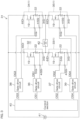
- Fig. 1 is a schematic view of a switching device 1 according to one embodiment of the present invention.
- Fig. 2 is an electrical circuit diagram of the switching device 1 in Fig. 1 .
- Fig. 1 to clarify the configuration of the switching device 1, one corner portion (broken-line hatched area) of a semiconductor chip 11 is shown transparently.
- the switching device 1 includes a resin package 2 having a flat rectangular-parallelepiped shape, a source terminal 3 (S) that is sealed on the resin package 2 and serves as an example of an output terminal of the present invention, a sense source terminal 4 (SS) as an example of a drive terminal of the present invention, a gate terminal 5 (G) and a drain terminal 6 (D).
- a resin package 2 having a flat rectangular-parallelepiped shape
- S source terminal 3
- SS sense source terminal 4
- G gate terminal 5
- D drain terminal 6
- the four terminals 3 to 6 are respectively formed of a metal plate in a predetermined shape, and are arranged in order from one side surface of the resin package 2 to a side surface opposed to it.
- each of the source terminal 3 and the drain terminal 6 is formed in a shape including islands 7, 8 in a rectangle shape and terminal portions 9, 10 in an elongated rectangle shape extending linearly from one side of these islands 7, 8.
- the sense source terminal 4 and the gate terminal 5 are formed in an elongated rectangle shape similar to the terminal portions 9, 10.
- the terminal portion 9 of the source terminal 3, the sense source terminal 4, the gate terminal 5, and the terminal portion 10 of the drain terminal 6 are arranged so as to be parallel one another.
- the semiconductor chip 11 as an example of an SiC switching element of the present invention is placed on the drain terminal 6 (center portion of the island 8).
- An almost entire rear surface of the semiconductor chip 11 is provided with a drain pad 12 as an example of a third electrode of the present invention, and this drain pad 12 is joined to the island 8.
- the drain pad 12 of the semiconductor chip 11 and the drain terminal 6 are electrically connected.
- a front surface of the semiconductor chip 11 is provided with a source pad 13 as an example of a second electrode of the present invention and a gate pad 14 as an example of a first electrode of the present invention.
- the source pad 13 has a generally square shape in a plan view, and is formed in a manner to cover almost an entire region of the front surface of the semiconductor chip 11.
- the source pad 13 is provided with a removal region 15 in a vicinity of a center of its one side.
- the removal region 15 is not provided with the source pad 13.
- the gate pad 14 is disposed on the removal region 15.
- the gate pad 14 and the source pad 13 are spaced apart and are insulated from each other.
- a plurality of source wires 16 are stretched as an example of a conductive member of the present invention between the source pad 13 and the source terminal 3, and the source pad 13 and the source terminal 3 are electrically connected by the source wires 16.
- four source wires 16 having the same length are arranged parallel to each other.
- a resistance of each source wire 16 can be unified to a constant value.
- a sense source wire 17 is stretched between the source terminal 3 (island 7) and the sense source terminal 4.
- the sense source terminal 4 is electrically connected to the source pad 13 via a current path including the sense source wire 17 and the source wires 16.
- an external resistance 22 having a resistance value r depending on a constituent material, a length, a wire diameter and the like of the source wire 16 can be connected in series between the sense source terminal 4 and the source pad 13.
- a position of the sense source is spaced from a source end (source pad 13) of the semiconductor chip 11, and a wire, wiring and the like intervene therebetween, whereby an external gate resistance (external resistance 22) which serves as a parasitic resistance when the gate-to-source voltage is applied to the semiconductor chip 11 is provided.
- a gate wire 18 (bonding wire) is stretched between the gate pad 14 and the gate terminal 5, and the gate pad 14 and the gate terminal 5 are electrically connected by the gate wire 18.
- the semiconductor chip 11 includes a MOSFET 19 using SiC (SiC-MOSFET) and a body diode 20.
- a source, a drain and a gate of the MOSFET 19 are electrically connected to the source pad 13, the drain pad 12 and the semiconductor chip 11, respectively.
- the switching element formed in the semiconductor chip 11 may be an element other than a MOSFET.
- this switching element may be SiC-IGBT, a SiC-bipolar transistor, SiC-JFET and the like.
- the source pad 13, the drain pad 12, the gate pad 14 and the sense source terminal 4 respectively correspond to an emitter pad, a collector pad, a gate pad and a sense emitter terminal of a SiC-IGBT.
- the switching element is a bipolar transistor
- the source pad 13, the drain pad 12, the gate pad 14 and the sense source terminal 4 respectively correspond to an emitter pad, a collector pad, a base pad and a sense emitter terminal of a SiC-bipolar transistor.
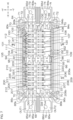
- Fig. 3 is an electrical circuit diagram of an inverter circuit 31 according to an embodiment of the present invention.
- Fig. 4 is an electrical circuit diagram showing an electrical configuration of a switching module 43 to which a plurality of the switching devices 1 in Fig. 1 are installed.
- the inverter circuit 31 as an example of an electrical circuit of the present invention includes first to fourth switching devices 32 to 35, first to fourth gate drive circuits 36 to 39, and a control section 40.
- each first switching element Tr1 is connected to the first gate terminal conductor layer 104 via a wire 111.
- Each first connection metal member 110 is connected to the first source-sense-terminal conductor layer 105 via a wire 112. That is, the source electrode of each first switching element Tr1 is connected to the first source-sense-terminal conductor layer 105 via the solder 136, the first connection metal member 110 and the wire 112.
- the second switching element Tr2 and the second diode element Di2 aligned in the Y direction are connected to the N-terminal conductor layer 107 by a second connection metal member 120 extending generally in the Y direction in a plan view.
- the second connection metal member 120 comprises a block-shaped standing portion whose base end portion is joined to the N-terminal conductor layer 107 via a solder 139 and whose tip end portion extends in the +Z direction, and a plate-shaped traverse portion extending from the tip end portion of the standing portion in the +Y direction and disposed above the second switching element Tr2 and the second diode element Di2.
- the fourth element joining conductor layer 206 has a T shape in a plan view, is disposed between the third element joining conductor layer 203 and the source conductor layer 207, and includes an element joining portion 206a having a rectangular shape elongated in the X direction in a plan view and an output terminal joining portion 206b extending along a side of the second insulating substrate 201 on the -X direction side. An end portion of the element joining portion 206a on the -X direction side is coupled to a length center portion of the output terminal joining portion 206b.
- the third gate terminal conductor layer 204 is disposed between the third element joining conductor layer 203 and a side of the second insulating substrate 201 on the +Y direction side, and has a rectangular shape elongated in the X direction in a plan view.
- the third source-sense-terminal conductor layer 205 is disposed between the third gate terminal conductor layer 204 and the side of the second insulating substrate 201 on the +Y direction side, and has a rectangular shape elongated in the X direction in a plan view.
- the comb-shaped terminal 86c can easily be ultrasonically joined to the output terminal joining portion 206b by pressing a head for ultrasonic joining against a tip of the comb-shaped terminal 86c, for example.
- the base end portion of the first gate terminal G1 is joined to the third gate terminal conductor layer 204.
- the base end portion of the first source sense terminal SS1 is joined to the third source-sense-terminal conductor layer 205. Joining of them may be performed by ultrasonic joining.
- drain electrodes of the plurality of third switching elements Tr3 are joined via a solder layer 232 (see Fig. 9 ), and at the same time, cathode electrodes of the plurality of third diode elements Di3 are joined via a solder layer 233.
- Each third switching element Tr3 has a source electrode and a gate electrode on a surface opposite to a surface joined to the third element joining conductor layer 203.
- Each third diode element Di3 has an anode electrode on a surface opposite to a surface joined to the third element joining conductor layer 203.
- a tip end portion of the traverse portion is joined to the anode electrode of the third diode element Di3 via a solder 235, and a length intermediate portion of the traverse portion is joined to the source electrode of the third switching element Tr3 via a solder 236.
- a width (length in the X direction) of the third connection metal member 210 is shorter than a width (length in the X direction) of the third switching element Tr3.
- the traverse portion of the third connection metal member 210 passes an intermediate portion of the width of the third switching element Tr3 in a plan view.
- five fourth switching elements Tr4 are disposed side by side in a manner spaced in the X direction. Further, between a side of the fourth element joining conductor layer 206 on the +Y direction side and the five fourth switching elements Tr4, five fourth diode elements Di4 are disposed side by side in a manner spaced in the X direction. The five fourth diode elements Di4 are aligned with the five fourth switching elements Tr4 with respect to the Y direction. Further, the five fourth diode elements Di4 are also aligned with the five third switching elements Tr3 with respect to the Y direction.
- the fourth switching element Tr4 and the fourth diode element Di4 aligned in the Y direction are connected to the source conductor layer 207 by a fourth connection metal member 220 extending generally in the Y direction in a plan view.
- the fourth connection metal member 220 comprises a block-shaped standing portion whose base end portion is joined to the source conductor layer 207 via a solder 239 and whose tip end portion extends in the +Z direction, and a plate-shaped traverse portion extending from the tip end portion of the standing portion and disposed above the fourth switching element Tr4 and the fourth diode element Di4.
- each fourth switching element Tr4 is connected to the fourth gate terminal conductor layer 208 via a wire 221.
- the third element joining conductor layer 203 of the second assembly 200 is connected to the first element joining conductor layer 103 of the first assembly 100 by a first conductor layer connecting member 91.
- the first conductor layer connecting member 91 comprises a plate-shaped body having an H shape in a plan view, and is formed of a pair of rectangular portions across the third element joining conductor layer 203 and the first element joining conductor layer 103 as well as a linking portion linking center portions of these rectangular portions. Since the first element joining conductor layer 103 and the third element joining conductor layer 203 are connected by the first conductor layer connecting member 91, reduction in inductance can be planned to achieve in comparison to a case of connecting by a wire, for example.
- the first conductor layer connecting member 91 has the H shape in a plan view, and a terminal of the first conductor layer connecting member 91 has a comb shape. Therefore, when the first conductor layer connecting member 91 is joined to the first element joining conductor layer 103, for example, the first conductor layer connecting member 91 can easily be ultrasonically joined to the first element joining conductor layer 103 by pressing a head for ultrasonic joining against a tip of the first conductor layer connecting member 91.
- the fourth element joining conductor layer 206 of the second assembly 200 is connected to the second element joining conductor layer 106 of the first assembly 100 by a second conductor layer connecting member 92.
- the second conductor layer connecting member 92 comprises a plate-shaped body having an H shape in a plan view, and is formed of a pair of rectangular portions across the fourth element joining conductor layer 206 and the second element joining conductor layer 106 as well as a linking portion linking center portions of these rectangular portions. Since the second element joining conductor layer 106 and the fourth element joining conductor layer 206 are connected by the second conductor layer connecting member 92, reduction in inductance can be planned to achieve in comparison to a case of connecting by a wire, for example.
- the second conductor layer connecting member 92 has the H shape in a plan view, and a terminal of the second conductor layer connecting member 92 has a comb shape. Therefore, when the second conductor layer connecting member 92 is joined to the second element joining conductor layer 106, for example, the second conductor layer connecting member 92 can easily be ultrasonically joined to the second element joining conductor layer 106 by pressing a head for ultrasonic joining against a tip of the second conductor layer connecting member 92.
- the source conductor layer 207 of the second assembly 200 is connected to the N-terminal conductor layer 107 of the first assembly 100 by a third conductor layer connecting member 93.
- the third conductor layer connecting member 93 comprises a plate-shaped body having an H shape in a plan view, and is formed of a pair of rectangular portions across the source conductor layer 207 and the N-terminal conductor layer 107 as well as a linking portion linking center portions of these rectangular portions. Since the N-terminal conductor layer 107 and the source conductor layer 207 are connected by the third conductor layer connecting member 93, reduction in inductance can be planned to achieve in comparison to a case of connecting by a wire, for example.
- the third conductor layer connecting member 93 has the H shape in a plan view, and a terminal of the third conductor layer connecting member 93 has a comb shape. Therefore, when the third conductor layer connecting member 93 is joined to the N-terminal conductor layer 107, for example, the third conductor layer connecting member 93 can easily be ultrasonically joined to the N-terminal conductor layer 107 by pressing a head for ultrasonic joining against a tip of the third conductor layer connecting member 93.
- the third gate terminal conductor layer 204 of the second assembly 200 is connected to the first gate terminal conductor layer 104 of the first assembly 100 via a wire 94.
- the third source-sense-terminal conductor layer 205 of the second assembly 200 is connected to the first source-sense-terminal conductor layer 105 of the first assembly 100 via a wire 95.
- the fourth gate terminal conductor layer 208 of the second assembly 200 is connected to the second gate terminal conductor layer 108 of the first assembly 100 via a wire 96.
- Fig. 10 is an electrical circuit diagram showing an electrical configuration of the semiconductor module 61.
- Fig. 10 shows the two output terminals OUT1, OUT2 as one output terminal OUT.
- the plurality of first switching elements Tr1 and the plurality of first diode elements Di1 provided on the first assembly 100 as well as the plurality of third switching elements Tr3 and the plurality of third diode elements Di3 provided on the second assembly 200 are parallelly connected between the first power-supply terminal P and the output terminal OUT to form an upper arm circuit (high side circuit) 301.
- the plurality of second switching elements Tr2 and the plurality of second diode elements Di2 provided on the first assembly 100 as well as the plurality of fourth switching elements Tr4 and the plurality of fourth diode elements Di4 provided on the second assembly 200 are connected between the output terminal OUT and the second power-supply terminal N to form a lower arm circuit (low side circuit) 302.
- the upper arm circuit 301 and the lower arm circuit 302 are connected in series between the first power-supply terminal P and the second power-supply terminal N, and the output terminal OUT is connected to a connecting point 303 between the upper arm circuit 301 and the lower arm circuit 302.
- a half bridge circuit is configured.
- This half bridge circuit can be used as a single-phase bridge circuit.
- a multi-phase (for example, three-phase) bridge circuit can be configured by parallelly connecting a plurality (for example, three) of the half bridge circuits (semiconductor module 1) to the power source.
- the first to fourth switching elements Tr1 to Tr4 are configured of N-channel DMOS (Double-Diffused Metal Oxide Semiconductor) field effect transistors.
- the first to fourth switching elements Tr1 to Tr4 are high-speed switching MOSFETs formed of SiC semiconductor devices (SiC-DMOS).
- the first diode element Di1 is parallelly connected to each first switching element Tr1.
- the third diode element Di3 is parallelly connected to each third switching element Tr3.
- the respective drains of each first switching element Tr1 and each third switching element Tr3 as well as the respective cathodes of each first diode element Di1 and each third diode element Di3 are connected to the first power-supply terminal P.
- the anodes of the plurality of first diode elements Di1 are connected to the sources of the corresponding first switching elements Tr1, and the sources of the first switching elements Tr1 are connected to the output terminal OUT.
- the anodes of the plurality of third diode elements Di3 are connected to the sources of the corresponding third switching elements Tr3, and the sources of the third switching elements Tr3 are connected to the output terminal OUT.
- the source of the first switching element Tr1 is connected to the first source sense terminal SS1 via the solder 136, the first connection metal member 110, the wire 112, the first source-sense-terminal conductor layer 105, the wire 95 and the third source-sense-terminal conductor layer 205. Therefore, there exists between the source of the first switching element Tr1 and the first source sense terminal SS1 a wiring resistance including a resistance (external resistance) R1 parasiting in a current path formed of the solder 136 and the first connection metal member 110.
- the wiring resistance between the source of the first switching element Tr1 and the first source sense terminal SS1 is larger by an amount of the external resistance R1 in comparison to a case of directly connecting one end of the wire 112 to the source of the first switching element Tr1.
- the source of the third switching element Tr3 is connected to the first source sense terminal SS1 via the solder 236, the third connection metal member 210, the wire 212 and the third source-sense-terminal conductor layer 205. Therefore, there exists between the source of the third switching element Tr3 and the first source sense terminal SS1 a wiring resistance including a resistance (external resistance) R3 parasiting in a current path formed of the solder 236 and the third connection metal member 210.
- the wiring resistance between the source of the third switching element Tr3 and the first source sense terminal SS1 is larger by an amount of the external resistance R3 in comparison to a case of directly connecting one end of the wire 212 to the source of the third switching element Tr3.
- the second diode element Di2 is parallelly connected to each second switching element Tr2.
- the fourth diode element Di4 is parallelly connected to each fourth switching element Tr4.
- the respective drains of each second switching element Tr2 and each fourth switching element Tr4 as well as the respective cathodes of each second diode element Di2 and each fourth diode element Di4 are connected to the output terminal OUT.
- the anodes of the plurality of second diode elements Di2 are connected to the sources of the corresponding second switching elements Tr2, and the sources of the second switching elements Tr2 are connected to the second power-supply terminal N.
- the anodes of the plurality of fourth diode elements Di4 are connected to the sources of the corresponding fourth switching elements Tr4, and the sources of the fourth switching elements Tr4 are connected to the second power-supply terminal N.
- the wiring resistance between the source of the fourth switching element Tr4 and the second source sense terminal SS2 is larger by an amount of the external resistance R4 in comparison to a case of directly connecting the source of the fourth switching element Tr4 and the second source-sense-terminal conductor layer 109 by a wire.
Landscapes
- Engineering & Computer Science (AREA)
- Power Engineering (AREA)
- Microelectronics & Electronic Packaging (AREA)
- Physics & Mathematics (AREA)
- General Physics & Mathematics (AREA)
- Inverter Devices (AREA)
- Ceramic Engineering (AREA)
- Chemical & Material Sciences (AREA)
- Power Conversion In General (AREA)
- Wire Bonding (AREA)
- Semiconductor Integrated Circuits (AREA)
- Junction Field-Effect Transistors (AREA)
- Metal-Oxide And Bipolar Metal-Oxide Semiconductor Integrated Circuits (AREA)
- Electronic Switches (AREA)
Applications Claiming Priority (3)
| Application Number | Priority Date | Filing Date | Title |
|---|---|---|---|
| JP2013240105 | 2013-11-20 | ||
| EP14863596.4A EP3073641A4 (de) | 2013-11-20 | 2014-11-18 | Schaltvorrichtung und elektronische schaltung |
| PCT/JP2014/080497 WO2015076257A1 (ja) | 2013-11-20 | 2014-11-18 | スイッチングデバイスおよび電子回路 |
Related Parent Applications (1)
| Application Number | Title | Priority Date | Filing Date |
|---|---|---|---|
| EP14863596.4A Division EP3073641A4 (de) | 2013-11-20 | 2014-11-18 | Schaltvorrichtung und elektronische schaltung |
Publications (2)
| Publication Number | Publication Date |
|---|---|
| EP4579736A2 true EP4579736A2 (de) | 2025-07-02 |
| EP4579736A3 EP4579736A3 (de) | 2025-12-31 |
Family
ID=53179519
Family Applications (4)
| Application Number | Title | Priority Date | Filing Date |
|---|---|---|---|
| EP24180651.2A Active EP4404464B1 (de) | 2013-11-20 | 2014-11-18 | Schaltvorrichtung und elektronische schaltung |
| EP14863596.4A Pending EP3073641A4 (de) | 2013-11-20 | 2014-11-18 | Schaltvorrichtung und elektronische schaltung |
| EP23168710.4A Pending EP4220708A1 (de) | 2013-11-20 | 2014-11-18 | Schaltvorrichtung und elektronische schaltung |
| EP25176571.5A Pending EP4579736A3 (de) | 2013-11-20 | 2014-11-18 | Schaltvorrichtung und elektronische schaltung |
Family Applications Before (3)
| Application Number | Title | Priority Date | Filing Date |
|---|---|---|---|
| EP24180651.2A Active EP4404464B1 (de) | 2013-11-20 | 2014-11-18 | Schaltvorrichtung und elektronische schaltung |
| EP14863596.4A Pending EP3073641A4 (de) | 2013-11-20 | 2014-11-18 | Schaltvorrichtung und elektronische schaltung |
| EP23168710.4A Pending EP4220708A1 (de) | 2013-11-20 | 2014-11-18 | Schaltvorrichtung und elektronische schaltung |
Country Status (5)
| Country | Link |
|---|---|
| US (9) | US10263612B2 (de) |
| EP (4) | EP4404464B1 (de) |
| JP (10) | JP6502263B2 (de) |
| CN (2) | CN105723619A (de) |
| WO (1) | WO2015076257A1 (de) |
Families Citing this family (42)
| Publication number | Priority date | Publication date | Assignee | Title |
|---|---|---|---|---|
| CN105723619A (zh) * | 2013-11-20 | 2016-06-29 | 罗姆股份有限公司 | 开关器件及电子电路 |
| JP6354392B2 (ja) * | 2014-07-03 | 2018-07-11 | 株式会社デンソー | 半導体装置 |
| JP6337789B2 (ja) * | 2015-02-04 | 2018-06-06 | 株式会社オートネットワーク技術研究所 | 電流検出回路、電流検出装置及び切替え装置 |
| JP6480856B2 (ja) * | 2015-12-14 | 2019-03-13 | 株式会社東芝 | 半導体モジュール |
| JP6529040B2 (ja) * | 2016-03-30 | 2019-06-12 | 東芝三菱電機産業システム株式会社 | 電力変換装置及びその制御方法 |
| JP6862722B2 (ja) * | 2016-09-01 | 2021-04-21 | 富士電機株式会社 | 電力変換装置 |
| US11367669B2 (en) | 2016-11-21 | 2022-06-21 | Rohm Co., Ltd. | Power module and fabrication method of the same, graphite plate, and power supply equipment |
| JP6470328B2 (ja) | 2017-02-09 | 2019-02-13 | 株式会社東芝 | 半導体モジュール |
| JP6786416B2 (ja) * | 2017-02-20 | 2020-11-18 | 株式会社東芝 | 半導体装置 |
| CN108511411B (zh) * | 2017-02-28 | 2021-09-10 | 株式会社村田制作所 | 半导体装置 |
| US11227862B2 (en) | 2017-02-28 | 2022-01-18 | Murata Manufacturing Co., Ltd. | Semiconductor device |
| JP6855998B2 (ja) * | 2017-10-18 | 2021-04-07 | 株式会社オートネットワーク技術研究所 | 車載用の半導体スイッチ装置及び車載用電源装置 |
| JP6819540B2 (ja) * | 2017-10-23 | 2021-01-27 | 三菱電機株式会社 | 半導体装置 |
| WO2019102694A1 (ja) * | 2017-11-27 | 2019-05-31 | 住友電気工業株式会社 | 半導体装置 |
| JP7025948B2 (ja) * | 2018-02-13 | 2022-02-25 | ローム株式会社 | 半導体装置および半導体装置の製造方法 |
| WO2020059751A1 (ja) * | 2018-09-19 | 2020-03-26 | ローム株式会社 | 半導体装置 |
| JP7187992B2 (ja) * | 2018-11-06 | 2022-12-13 | 富士電機株式会社 | 半導体モジュールおよび車両 |
| JP7485662B2 (ja) * | 2019-05-20 | 2024-05-16 | ローム株式会社 | 半導体装置 |
| US11069640B2 (en) * | 2019-06-14 | 2021-07-20 | Cree Fayetteville, Inc. | Package for power electronics |
| JP7198168B2 (ja) * | 2019-07-19 | 2022-12-28 | 株式会社 日立パワーデバイス | パワー半導体モジュール |
| WO2021049434A1 (ja) * | 2019-09-11 | 2021-03-18 | 富士電機株式会社 | 電流生成回路、駆動回路及び電流調整方法 |
| JP6875588B1 (ja) * | 2020-09-18 | 2021-05-26 | 住友電気工業株式会社 | 半導体装置 |
| JP7286582B2 (ja) | 2020-03-24 | 2023-06-05 | 株式会社東芝 | 半導体装置 |
| US20230163055A1 (en) * | 2020-04-01 | 2023-05-25 | Panasonic Intellectual Property Management Co., Ltd. | Semiconductor module |
| DE102020205420A1 (de) * | 2020-04-29 | 2021-11-04 | Zf Friedrichshafen Ag | Halbbrückenmodul für einen Inverter eines elektrischen Antriebs eines Elektrofahrzeugs oder eines Hybridfahrzeugs und Inverter für einen elektrischen Antrieb eines Elektrofahrzeugs oder eines Hybridfahrzeugs |
| JP2021177519A (ja) * | 2020-05-08 | 2021-11-11 | 株式会社東芝 | 半導体装置 |
| JP7491043B2 (ja) | 2020-05-13 | 2024-05-28 | 富士電機株式会社 | 半導体モジュール |
| CN115552597A (zh) * | 2020-05-19 | 2022-12-30 | 三菱电机株式会社 | 半导体模块 |
| CN112054706A (zh) * | 2020-07-23 | 2020-12-08 | 华为技术有限公司 | 半导体功率模块及其电流检测方法、制造方法与汽车 |
| JP7563036B2 (ja) * | 2020-08-11 | 2024-10-08 | 富士電機株式会社 | スイッチング装置および判定装置 |
| CN114365407B (zh) * | 2020-08-12 | 2023-05-09 | 华为数字能源技术有限公司 | 图腾柱无桥功率因数校正电路和电力电子设备 |
| JP7463909B2 (ja) * | 2020-08-25 | 2024-04-09 | 株式会社デンソー | 半導体装置及びその製造方法 |
| JP7538764B2 (ja) * | 2021-03-30 | 2024-08-22 | 三菱電機株式会社 | 半導体モジュール |
| JPWO2023286531A1 (de) * | 2021-07-13 | 2023-01-19 | ||
| JPWO2023021938A1 (de) * | 2021-08-18 | 2023-02-23 | ||
| JP2023069403A (ja) * | 2021-11-05 | 2023-05-18 | 富士電機株式会社 | 半導体モジュール及びその故障素子判定方法 |
| JP7826664B2 (ja) * | 2021-11-30 | 2026-03-10 | 富士電機株式会社 | 半導体モジュール、半導体装置、及び車両 |
| JP7826665B2 (ja) * | 2021-11-30 | 2026-03-10 | 富士電機株式会社 | 半導体モジュール、半導体装置、及び車両 |
| KR20230095546A (ko) * | 2021-12-22 | 2023-06-29 | 주식회사 엘엑스세미콘 | 전력반도체모듈 및 그 제조방법 |
| JP7803430B2 (ja) * | 2022-10-31 | 2026-01-21 | 富士電機株式会社 | 半導体モジュール |
| DE102022134657A1 (de) | 2022-12-22 | 2024-06-27 | Valeo Eautomotive Germany Gmbh | Leistungsmodul, elektrischer Leistungswandler und elektrischer Antrieb für ein Transportmittel |
| CN119948629A (zh) * | 2023-04-12 | 2025-05-06 | 富士电机株式会社 | 半导体模块 |
Citations (2)
| Publication number | Priority date | Publication date | Assignee | Title |
|---|---|---|---|---|
| JP2005137072A (ja) | 2003-10-29 | 2005-05-26 | Nissan Motor Co Ltd | 過電流保護回路 |
| JP2013240105A (ja) | 2009-10-19 | 2013-11-28 | Murata Mfg Co Ltd | 弾性表面波装置 |
Family Cites Families (38)
| Publication number | Priority date | Publication date | Assignee | Title |
|---|---|---|---|---|
| JPH05276761A (ja) * | 1992-03-19 | 1993-10-22 | Hitachi Ltd | パワー半導体素子の過電流検出方法及び回路並びにこれを用いたインバータ装置 |
| US5917203A (en) * | 1996-07-29 | 1999-06-29 | Motorola, Inc. | Lateral gate vertical drift region transistor |
| JP3675603B2 (ja) * | 1997-03-19 | 2005-07-27 | 株式会社ルネサス東日本セミコンダクタ | 半導体装置 |
| JPH11121683A (ja) * | 1997-10-08 | 1999-04-30 | Nissan Motor Co Ltd | 半導体集積回路 |
| JP2000049184A (ja) | 1998-05-27 | 2000-02-18 | Hitachi Ltd | 半導体装置およびその製造方法 |
| EP1014403A1 (de) * | 1998-12-21 | 2000-06-28 | Asea Brown Boveri AG | Strombegrenzender Schalter |
| EP1143604B1 (de) * | 1999-06-29 | 2007-09-26 | Mitsubishi Denki Kabushiki Kaisha | Stromwandlervorrichtung |
| JP2001274322A (ja) | 2000-03-27 | 2001-10-05 | Mitsubishi Electric Corp | パワー半導体モジュール |
| JP4110513B2 (ja) | 2002-05-01 | 2008-07-02 | 富士電機ホールディングス株式会社 | 半導体パワーモジュールの製造方法 |
| JP4220731B2 (ja) | 2002-06-19 | 2009-02-04 | 三菱電機株式会社 | 電力用半導体装置 |
| JP3896940B2 (ja) * | 2002-10-08 | 2007-03-22 | 三菱電機株式会社 | 半導体装置 |
| JP4342232B2 (ja) * | 2003-07-11 | 2009-10-14 | 三菱電機株式会社 | 半導体パワーモジュールおよび該モジュールの主回路電流値を計測する主回路電流計測システム |
| JP2005051109A (ja) * | 2003-07-30 | 2005-02-24 | Matsushita Electric Ind Co Ltd | パワー半導体モジュール |
| JP2005113695A (ja) * | 2003-10-03 | 2005-04-28 | Matsushita Electric Ind Co Ltd | 電子回路装置付きコンプレッサ |
| JP2006109665A (ja) * | 2004-10-08 | 2006-04-20 | Denso Corp | 過電流検出機能を有する集積回路装置 |
| JP4547231B2 (ja) | 2004-10-22 | 2010-09-22 | 日立オートモティブシステムズ株式会社 | 電力変換装置 |
| JP4712024B2 (ja) * | 2007-12-12 | 2011-06-29 | 三菱電機株式会社 | 半導体電力変換装置の過電流保護装置 |
| JP2009176804A (ja) * | 2008-01-22 | 2009-08-06 | Nippon Steel Corp | 電力変換素子 |
| JP5327646B2 (ja) * | 2009-06-24 | 2013-10-30 | 株式会社デンソー | 電子回路内蔵型モータ |
| US8697574B2 (en) * | 2009-09-25 | 2014-04-15 | Infineon Technologies Ag | Through substrate features in semiconductor substrates |
| JP2011182591A (ja) * | 2010-03-02 | 2011-09-15 | Panasonic Corp | 半導体装置 |
| JP2011254387A (ja) * | 2010-06-03 | 2011-12-15 | Rohm Co Ltd | 交流スイッチ |
| JP5267616B2 (ja) | 2010-07-29 | 2013-08-21 | 株式会社デンソー | 駆動制御装置 |
| JP5534076B2 (ja) | 2010-07-29 | 2014-06-25 | 株式会社デンソー | 駆動制御装置 |
| WO2012043146A1 (ja) * | 2010-09-28 | 2012-04-05 | 富士電機株式会社 | 半導体装置 |
| JP5995435B2 (ja) | 2011-08-02 | 2016-09-21 | ローム株式会社 | 半導体装置およびその製造方法 |
| JP2013093444A (ja) * | 2011-10-26 | 2013-05-16 | Rohm Co Ltd | 高速スイッチング動作回路 |
| JP5893369B2 (ja) * | 2011-12-05 | 2016-03-23 | ローム株式会社 | 半導体装置 |
| US8723178B2 (en) * | 2012-01-20 | 2014-05-13 | Monolithic Power Systems, Inc. | Integrated field effect transistors with high voltage drain sensing |
| JP5477669B2 (ja) * | 2012-02-28 | 2014-04-23 | 株式会社デンソー | 半導体モジュール |
| EP3018712B1 (de) * | 2013-07-05 | 2021-09-01 | Renesas Electronics Corporation | Halbleiterbauelement |
| CN105723619A (zh) * | 2013-11-20 | 2016-06-29 | 罗姆股份有限公司 | 开关器件及电子电路 |
| DE102015103247A1 (de) * | 2015-03-05 | 2016-09-08 | Ge Energy Power Conversion Technology Limited | Schaltmodul mit Kurzschlussschutz und Leistungselektronikmodul mit diesem |
| JP6510288B2 (ja) * | 2015-03-30 | 2019-05-08 | ローム株式会社 | チャージポンプ回路 |
| WO2017056176A1 (ja) * | 2015-09-29 | 2017-04-06 | 三菱電機株式会社 | 半導体装置およびそれを備える半導体モジュール |
| US10312167B2 (en) * | 2017-02-15 | 2019-06-04 | Infineon Technologies Ag | Semiconductor package, assembly and module arrangements for measuring gate-to-emitter/source voltage |
| JP6852011B2 (ja) * | 2018-03-21 | 2021-03-31 | 株式会社東芝 | 半導体装置 |
| JP7358921B2 (ja) * | 2019-11-08 | 2023-10-11 | 富士電機株式会社 | 半導体モジュール及び半導体モジュールの製造方法 |
-
2014
- 2014-11-18 CN CN201480063746.5A patent/CN105723619A/zh active Pending
- 2014-11-18 US US15/037,592 patent/US10263612B2/en active Active
- 2014-11-18 EP EP24180651.2A patent/EP4404464B1/de active Active
- 2014-11-18 EP EP14863596.4A patent/EP3073641A4/de active Pending
- 2014-11-18 EP EP23168710.4A patent/EP4220708A1/de active Pending
- 2014-11-18 JP JP2015549156A patent/JP6502263B2/ja active Active
- 2014-11-18 CN CN202011022376.4A patent/CN112117997B/zh active Active
- 2014-11-18 WO PCT/JP2014/080497 patent/WO2015076257A1/ja not_active Ceased
- 2014-11-18 EP EP25176571.5A patent/EP4579736A3/de active Pending
-
2019
- 2019-02-06 JP JP2019020031A patent/JP6650061B2/ja active Active
- 2019-02-07 US US16/270,248 patent/US10826481B2/en active Active
-
2020
- 2020-01-17 JP JP2020006028A patent/JP6823737B2/ja active Active
- 2020-10-14 US US17/070,496 patent/US11336275B2/en active Active
-
2021
- 2021-01-08 JP JP2021002409A patent/JP6923769B2/ja active Active
- 2021-07-29 JP JP2021124317A patent/JP7261268B2/ja active Active
-
2022
- 2022-04-18 US US17/722,967 patent/US11728801B2/en active Active
-
2023
- 2023-04-07 JP JP2023062661A patent/JP7373687B2/ja active Active
- 2023-04-07 JP JP2023062662A patent/JP7457858B2/ja active Active
- 2023-04-07 JP JP2023062660A patent/JP7457857B2/ja active Active
- 2023-04-25 US US18/306,713 patent/US12068741B2/en active Active
- 2023-04-25 US US18/306,707 patent/US12063030B2/en active Active
- 2023-04-25 US US18/306,703 patent/US11936369B2/en active Active
-
2024
- 2024-03-15 JP JP2024041430A patent/JP2024069507A/ja active Pending
- 2024-04-23 US US18/643,469 patent/US12316307B2/en active Active
-
2025
- 2025-04-11 US US19/176,804 patent/US20250240006A1/en active Pending
- 2025-11-10 JP JP2025188805A patent/JP2026012435A/ja active Pending
Patent Citations (2)
| Publication number | Priority date | Publication date | Assignee | Title |
|---|---|---|---|---|
| JP2005137072A (ja) | 2003-10-29 | 2005-05-26 | Nissan Motor Co Ltd | 過電流保護回路 |
| JP2013240105A (ja) | 2009-10-19 | 2013-11-28 | Murata Mfg Co Ltd | 弾性表面波装置 |
Also Published As
Similar Documents
| Publication | Publication Date | Title |
|---|---|---|
| US12068741B2 (en) | Switching device and electronic circuit | |
| US10607978B2 (en) | Semiconductor device and electronic apparatus | |
| EP3573096B1 (de) | Halbleitermodul | |
| JP5893369B2 (ja) | 半導体装置 |
Legal Events
| Date | Code | Title | Description |
|---|---|---|---|
| PUAI | Public reference made under article 153(3) epc to a published international application that has entered the european phase |
Free format text: ORIGINAL CODE: 0009012 |
|
| STAA | Information on the status of an ep patent application or granted ep patent |
Free format text: STATUS: REQUEST FOR EXAMINATION WAS MADE |
|
| 17P | Request for examination filed |
Effective date: 20250515 |
|
| AC | Divisional application: reference to earlier application |
Ref document number: 3073641 Country of ref document: EP Kind code of ref document: P |
|
| AK | Designated contracting states |
Kind code of ref document: A2 Designated state(s): AL AT BE BG CH CY CZ DE DK EE ES FI FR GB GR HR HU IE IS IT LI LT LU LV MC MK MT NL NO PL PT RO RS SE SI SK SM TR |
|
| REG | Reference to a national code |
Ref country code: DE Ref legal event code: R079 Free format text: PREVIOUS MAIN CLASS: H01L0023495000 Ipc: H01L0023490000 |
|
| PUAL | Search report despatched |
Free format text: ORIGINAL CODE: 0009013 |
|
| AK | Designated contracting states |
Kind code of ref document: A3 Designated state(s): AL AT BE BG CH CY CZ DE DK EE ES FI FR GB GR HR HU IE IS IT LI LT LU LV MC MK MT NL NO PL PT RO RS SE SI SK SM TR |
|
| RIC1 | Information provided on ipc code assigned before grant |
Ipc: H01L 23/49 20060101AFI20251127BHEP Ipc: H01L 23/495 20060101ALI20251127BHEP Ipc: H01L 23/31 20060101ALI20251127BHEP Ipc: H02H 3/20 20060101ALI20251127BHEP Ipc: H03K 17/08 20060101ALI20251127BHEP Ipc: H01L 25/07 20060101ALI20251127BHEP Ipc: H01L 25/18 20230101ALI20251127BHEP Ipc: H02H 9/04 20060101ALI20251127BHEP Ipc: H02M 7/5387 20070101ALI20251127BHEP Ipc: H03K 17/082 20060101ALI20251127BHEP Ipc: H03K 17/12 20060101ALI20251127BHEP Ipc: H01L 23/00 20060101ALI20251127BHEP |