JP6875588B1 - 半導体装置 - Google Patents
半導体装置 Download PDFInfo
- Publication number
- JP6875588B1 JP6875588B1 JP2020157444A JP2020157444A JP6875588B1 JP 6875588 B1 JP6875588 B1 JP 6875588B1 JP 2020157444 A JP2020157444 A JP 2020157444A JP 2020157444 A JP2020157444 A JP 2020157444A JP 6875588 B1 JP6875588 B1 JP 6875588B1
- Authority
- JP
- Japan
- Prior art keywords
- insulating substrate
- terminal
- conductive layer
- conductor
- transistor
- Prior art date
- Legal status (The legal status is an assumption and is not a legal conclusion. Google has not performed a legal analysis and makes no representation as to the accuracy of the status listed.)
- Active
Links
- 239000004065 semiconductor Substances 0.000 title claims abstract description 57
- 239000000758 substrate Substances 0.000 claims abstract description 170
- 239000004020 conductor Substances 0.000 claims description 88
- HBMJWWWQQXIZIP-UHFFFAOYSA-N silicon carbide Chemical compound [Si+]#[C-] HBMJWWWQQXIZIP-UHFFFAOYSA-N 0.000 claims description 11
- 229910010271 silicon carbide Inorganic materials 0.000 claims description 11
- 229910052751 metal Inorganic materials 0.000 claims description 7
- 239000002184 metal Substances 0.000 claims description 7
- 230000005669 field effect Effects 0.000 claims description 6
- 230000004888 barrier function Effects 0.000 claims description 5
- 238000010586 diagram Methods 0.000 abstract description 7
- 239000000463 material Substances 0.000 description 15
- 229910000679 solder Inorganic materials 0.000 description 10
- 230000017525 heat dissipation Effects 0.000 description 3
- 239000010949 copper Substances 0.000 description 2
- 238000009413 insulation Methods 0.000 description 2
- 230000007257 malfunction Effects 0.000 description 2
- 230000004048 modification Effects 0.000 description 2
- 238000012986 modification Methods 0.000 description 2
- RYGMFSIKBFXOCR-UHFFFAOYSA-N Copper Chemical compound [Cu] RYGMFSIKBFXOCR-UHFFFAOYSA-N 0.000 description 1
- 229910000881 Cu alloy Inorganic materials 0.000 description 1
- 229910052782 aluminium Inorganic materials 0.000 description 1
- XAGFODPZIPBFFR-UHFFFAOYSA-N aluminium Chemical compound [Al] XAGFODPZIPBFFR-UHFFFAOYSA-N 0.000 description 1
- 229910052802 copper Inorganic materials 0.000 description 1
- 230000000694 effects Effects 0.000 description 1
- 239000012212 insulator Substances 0.000 description 1
- 239000011347 resin Substances 0.000 description 1
- 229920005989 resin Polymers 0.000 description 1
Images


Classifications
-
- H—ELECTRICITY
- H01—ELECTRIC ELEMENTS
- H01L—SEMICONDUCTOR DEVICES NOT COVERED BY CLASS H10
- H01L23/00—Details of semiconductor or other solid state devices
- H01L23/34—Arrangements for cooling, heating, ventilating or temperature compensation ; Temperature sensing arrangements
- H01L23/36—Selection of materials, or shaping, to facilitate cooling or heating, e.g. heatsinks
- H01L23/373—Cooling facilitated by selection of materials for the device or materials for thermal expansion adaptation, e.g. carbon
- H01L23/3735—Laminates or multilayers, e.g. direct bond copper ceramic substrates
-
- H—ELECTRICITY
- H01—ELECTRIC ELEMENTS
- H01L—SEMICONDUCTOR DEVICES NOT COVERED BY CLASS H10
- H01L21/00—Processes or apparatus adapted for the manufacture or treatment of semiconductor or solid state devices or of parts thereof
- H01L21/02—Manufacture or treatment of semiconductor devices or of parts thereof
- H01L21/04—Manufacture or treatment of semiconductor devices or of parts thereof the devices having at least one potential-jump barrier or surface barrier, e.g. PN junction, depletion layer or carrier concentration layer
- H01L21/50—Assembly of semiconductor devices using processes or apparatus not provided for in a single one of the subgroups H01L21/06 - H01L21/326, e.g. sealing of a cap to a base of a container
- H01L21/60—Attaching or detaching leads or other conductive members, to be used for carrying current to or from the device in operation
-
- H—ELECTRICITY
- H01—ELECTRIC ELEMENTS
- H01L—SEMICONDUCTOR DEVICES NOT COVERED BY CLASS H10
- H01L23/00—Details of semiconductor or other solid state devices
- H01L23/34—Arrangements for cooling, heating, ventilating or temperature compensation ; Temperature sensing arrangements
- H01L23/36—Selection of materials, or shaping, to facilitate cooling or heating, e.g. heatsinks
- H01L23/367—Cooling facilitated by shape of device
- H01L23/3672—Foil-like cooling fins or heat sinks
-
- H—ELECTRICITY
- H01—ELECTRIC ELEMENTS
- H01L—SEMICONDUCTOR DEVICES NOT COVERED BY CLASS H10
- H01L23/00—Details of semiconductor or other solid state devices
- H01L23/52—Arrangements for conducting electric current within the device in operation from one component to another, i.e. interconnections, e.g. wires, lead frames
- H01L23/538—Arrangements for conducting electric current within the device in operation from one component to another, i.e. interconnections, e.g. wires, lead frames the interconnection structure between a plurality of semiconductor chips being formed on, or in, insulating substrates
- H01L23/5385—Assembly of a plurality of insulating substrates
-
- H—ELECTRICITY
- H01—ELECTRIC ELEMENTS
- H01L—SEMICONDUCTOR DEVICES NOT COVERED BY CLASS H10
- H01L24/00—Arrangements for connecting or disconnecting semiconductor or solid-state bodies; Methods or apparatus related thereto
- H01L24/01—Means for bonding being attached to, or being formed on, the surface to be connected, e.g. chip-to-package, die-attach, "first-level" interconnects; Manufacturing methods related thereto
- H01L24/42—Wire connectors; Manufacturing methods related thereto
- H01L24/47—Structure, shape, material or disposition of the wire connectors after the connecting process
- H01L24/48—Structure, shape, material or disposition of the wire connectors after the connecting process of an individual wire connector
-
- H—ELECTRICITY
- H01—ELECTRIC ELEMENTS
- H01L—SEMICONDUCTOR DEVICES NOT COVERED BY CLASS H10
- H01L25/00—Assemblies consisting of a plurality of individual semiconductor or other solid state devices ; Multistep manufacturing processes thereof
- H01L25/03—Assemblies consisting of a plurality of individual semiconductor or other solid state devices ; Multistep manufacturing processes thereof all the devices being of a type provided for in the same subgroup of groups H01L27/00 - H01L33/00, or in a single subclass of H10K, H10N, e.g. assemblies of rectifier diodes
- H01L25/04—Assemblies consisting of a plurality of individual semiconductor or other solid state devices ; Multistep manufacturing processes thereof all the devices being of a type provided for in the same subgroup of groups H01L27/00 - H01L33/00, or in a single subclass of H10K, H10N, e.g. assemblies of rectifier diodes the devices not having separate containers
- H01L25/07—Assemblies consisting of a plurality of individual semiconductor or other solid state devices ; Multistep manufacturing processes thereof all the devices being of a type provided for in the same subgroup of groups H01L27/00 - H01L33/00, or in a single subclass of H10K, H10N, e.g. assemblies of rectifier diodes the devices not having separate containers the devices being of a type provided for in group H01L29/00
- H01L25/072—Assemblies consisting of a plurality of individual semiconductor or other solid state devices ; Multistep manufacturing processes thereof all the devices being of a type provided for in the same subgroup of groups H01L27/00 - H01L33/00, or in a single subclass of H10K, H10N, e.g. assemblies of rectifier diodes the devices not having separate containers the devices being of a type provided for in group H01L29/00 the devices being arranged next to each other
-
- H—ELECTRICITY
- H01—ELECTRIC ELEMENTS
- H01L—SEMICONDUCTOR DEVICES NOT COVERED BY CLASS H10
- H01L25/00—Assemblies consisting of a plurality of individual semiconductor or other solid state devices ; Multistep manufacturing processes thereof
- H01L25/18—Assemblies consisting of a plurality of individual semiconductor or other solid state devices ; Multistep manufacturing processes thereof the devices being of types provided for in two or more different subgroups of the same main group of groups H01L27/00 - H01L33/00, or in a single subclass of H10K, H10N
-
- H—ELECTRICITY
- H01—ELECTRIC ELEMENTS
- H01L—SEMICONDUCTOR DEVICES NOT COVERED BY CLASS H10
- H01L29/00—Semiconductor devices adapted for rectifying, amplifying, oscillating or switching, or capacitors or resistors with at least one potential-jump barrier or surface barrier, e.g. PN junction depletion layer or carrier concentration layer; Details of semiconductor bodies or of electrodes thereof ; Multistep manufacturing processes therefor
- H01L29/02—Semiconductor bodies ; Multistep manufacturing processes therefor
- H01L29/12—Semiconductor bodies ; Multistep manufacturing processes therefor characterised by the materials of which they are formed
- H01L29/16—Semiconductor bodies ; Multistep manufacturing processes therefor characterised by the materials of which they are formed including, apart from doping materials or other impurities, only elements of Group IV of the Periodic System
- H01L29/1608—Silicon carbide
-
- H—ELECTRICITY
- H01—ELECTRIC ELEMENTS
- H01L—SEMICONDUCTOR DEVICES NOT COVERED BY CLASS H10
- H01L29/00—Semiconductor devices adapted for rectifying, amplifying, oscillating or switching, or capacitors or resistors with at least one potential-jump barrier or surface barrier, e.g. PN junction depletion layer or carrier concentration layer; Details of semiconductor bodies or of electrodes thereof ; Multistep manufacturing processes therefor
- H01L29/66—Types of semiconductor device ; Multistep manufacturing processes therefor
- H01L29/86—Types of semiconductor device ; Multistep manufacturing processes therefor controllable only by variation of the electric current supplied, or only the electric potential applied, to one or more of the electrodes carrying the current to be rectified, amplified, oscillated or switched
- H01L29/861—Diodes
- H01L29/872—Schottky diodes
-
- H—ELECTRICITY
- H01—ELECTRIC ELEMENTS
- H01L—SEMICONDUCTOR DEVICES NOT COVERED BY CLASS H10
- H01L2224/00—Indexing scheme for arrangements for connecting or disconnecting semiconductor or solid-state bodies and methods related thereto as covered by H01L24/00
- H01L2224/01—Means for bonding being attached to, or being formed on, the surface to be connected, e.g. chip-to-package, die-attach, "first-level" interconnects; Manufacturing methods related thereto
- H01L2224/02—Bonding areas; Manufacturing methods related thereto
- H01L2224/04—Structure, shape, material or disposition of the bonding areas prior to the connecting process
- H01L2224/06—Structure, shape, material or disposition of the bonding areas prior to the connecting process of a plurality of bonding areas
- H01L2224/0601—Structure
- H01L2224/0603—Bonding areas having different sizes, e.g. different heights or widths
-
- H—ELECTRICITY
- H01—ELECTRIC ELEMENTS
- H01L—SEMICONDUCTOR DEVICES NOT COVERED BY CLASS H10
- H01L2224/00—Indexing scheme for arrangements for connecting or disconnecting semiconductor or solid-state bodies and methods related thereto as covered by H01L24/00
- H01L2224/01—Means for bonding being attached to, or being formed on, the surface to be connected, e.g. chip-to-package, die-attach, "first-level" interconnects; Manufacturing methods related thereto
- H01L2224/42—Wire connectors; Manufacturing methods related thereto
- H01L2224/47—Structure, shape, material or disposition of the wire connectors after the connecting process
- H01L2224/48—Structure, shape, material or disposition of the wire connectors after the connecting process of an individual wire connector
- H01L2224/481—Disposition
- H01L2224/48151—Connecting between a semiconductor or solid-state body and an item not being a semiconductor or solid-state body, e.g. chip-to-substrate, chip-to-passive
- H01L2224/48221—Connecting between a semiconductor or solid-state body and an item not being a semiconductor or solid-state body, e.g. chip-to-substrate, chip-to-passive the body and the item being stacked
- H01L2224/48225—Connecting between a semiconductor or solid-state body and an item not being a semiconductor or solid-state body, e.g. chip-to-substrate, chip-to-passive the body and the item being stacked the item being non-metallic, e.g. insulating substrate with or without metallisation
- H01L2224/48227—Connecting between a semiconductor or solid-state body and an item not being a semiconductor or solid-state body, e.g. chip-to-substrate, chip-to-passive the body and the item being stacked the item being non-metallic, e.g. insulating substrate with or without metallisation connecting the wire to a bond pad of the item
-
- H—ELECTRICITY
- H01—ELECTRIC ELEMENTS
- H01L—SEMICONDUCTOR DEVICES NOT COVERED BY CLASS H10
- H01L2224/00—Indexing scheme for arrangements for connecting or disconnecting semiconductor or solid-state bodies and methods related thereto as covered by H01L24/00
- H01L2224/01—Means for bonding being attached to, or being formed on, the surface to be connected, e.g. chip-to-package, die-attach, "first-level" interconnects; Manufacturing methods related thereto
- H01L2224/42—Wire connectors; Manufacturing methods related thereto
- H01L2224/47—Structure, shape, material or disposition of the wire connectors after the connecting process
- H01L2224/48—Structure, shape, material or disposition of the wire connectors after the connecting process of an individual wire connector
- H01L2224/481—Disposition
- H01L2224/48151—Connecting between a semiconductor or solid-state body and an item not being a semiconductor or solid-state body, e.g. chip-to-substrate, chip-to-passive
- H01L2224/48221—Connecting between a semiconductor or solid-state body and an item not being a semiconductor or solid-state body, e.g. chip-to-substrate, chip-to-passive the body and the item being stacked
- H01L2224/48245—Connecting between a semiconductor or solid-state body and an item not being a semiconductor or solid-state body, e.g. chip-to-substrate, chip-to-passive the body and the item being stacked the item being metallic
- H01L2224/48247—Connecting between a semiconductor or solid-state body and an item not being a semiconductor or solid-state body, e.g. chip-to-substrate, chip-to-passive the body and the item being stacked the item being metallic connecting the wire to a bond pad of the item
-
- H—ELECTRICITY
- H01—ELECTRIC ELEMENTS
- H01L—SEMICONDUCTOR DEVICES NOT COVERED BY CLASS H10
- H01L2224/00—Indexing scheme for arrangements for connecting or disconnecting semiconductor or solid-state bodies and methods related thereto as covered by H01L24/00
- H01L2224/01—Means for bonding being attached to, or being formed on, the surface to be connected, e.g. chip-to-package, die-attach, "first-level" interconnects; Manufacturing methods related thereto
- H01L2224/42—Wire connectors; Manufacturing methods related thereto
- H01L2224/47—Structure, shape, material or disposition of the wire connectors after the connecting process
- H01L2224/49—Structure, shape, material or disposition of the wire connectors after the connecting process of a plurality of wire connectors
- H01L2224/491—Disposition
- H01L2224/4912—Layout
- H01L2224/49175—Parallel arrangements
-
- H—ELECTRICITY
- H01—ELECTRIC ELEMENTS
- H01L—SEMICONDUCTOR DEVICES NOT COVERED BY CLASS H10
- H01L23/00—Details of semiconductor or other solid state devices
- H01L23/52—Arrangements for conducting electric current within the device in operation from one component to another, i.e. interconnections, e.g. wires, lead frames
- H01L23/538—Arrangements for conducting electric current within the device in operation from one component to another, i.e. interconnections, e.g. wires, lead frames the interconnection structure between a plurality of semiconductor chips being formed on, or in, insulating substrates
- H01L23/5386—Geometry or layout of the interconnection structure
-
- H—ELECTRICITY
- H01—ELECTRIC ELEMENTS
- H01L—SEMICONDUCTOR DEVICES NOT COVERED BY CLASS H10
- H01L24/00—Arrangements for connecting or disconnecting semiconductor or solid-state bodies; Methods or apparatus related thereto
- H01L24/01—Means for bonding being attached to, or being formed on, the surface to be connected, e.g. chip-to-package, die-attach, "first-level" interconnects; Manufacturing methods related thereto
- H01L24/42—Wire connectors; Manufacturing methods related thereto
- H01L24/47—Structure, shape, material or disposition of the wire connectors after the connecting process
- H01L24/49—Structure, shape, material or disposition of the wire connectors after the connecting process of a plurality of wire connectors
-
- H—ELECTRICITY
- H01—ELECTRIC ELEMENTS
- H01L—SEMICONDUCTOR DEVICES NOT COVERED BY CLASS H10
- H01L2924/00—Indexing scheme for arrangements or methods for connecting or disconnecting semiconductor or solid-state bodies as covered by H01L24/00
- H01L2924/19—Details of hybrid assemblies other than the semiconductor or other solid state devices to be connected
- H01L2924/191—Disposition
- H01L2924/19101—Disposition of discrete passive components
- H01L2924/19107—Disposition of discrete passive components off-chip wires
Abstract
Description
以下、本開示の実施形態について詳細に説明するが、本実施形態はこれらに限定されるものではない。なお、本明細書及び図面において、実質的に同一の機能構成を有する構成要素については、同一の符号を付することにより重複した説明を省くことがある。
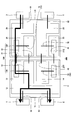
まず、第1実施形態について説明する。図1は、第1実施形態に係る半導体装置を示す斜視図である。図2は、第1実施形態に係る半導体装置を示す上面図である。ただし、図2では、ケースを透視している。図3は、第1実施形態に係る半導体装置における放熱板と、第1絶縁基板と、第2絶縁基板との関係を示す断面図である。図3は、図2中のIII-III線に沿った断面図に相当する。
次に、第2実施形態について説明する。図14は、第2実施形態に係る半導体装置における第1絶縁基板及び第2絶縁基板の構成を示す模式図である。
2:放熱板
2A:第1主面
2B:第2主面
3:P端子
4:N端子
5:第1O端子
6:第2O端子
7、8:接合材
9:ケース
10:第1絶縁基板
10A:第3絶縁基板
10B:第4絶縁基板
11、11A、11B、12A、12B、12C、13A、13B、14A、14B、18、18A、18B、19:導電層
12:第2導体、第7導体(導電層)
13:第1導体(導電層)
14:第8導体(導電層)
20:第2絶縁基板
20A:第5絶縁基板
20B:第6絶縁基板
21、21A、21B、22A、22B、23A、23B、24A、24B、25A、25B、26、27、28、28A、28B、29:導電層
22:第6導体(導電層)
23:第5導体(導電層)
24:第4導体(導電層)
25:第3導体(導電層)
31:第1接続部材(ワイヤ)
32:第2接続部材(ワイヤ)
41:第5接続部材(ワイヤ)
42:第6接続部材(ワイヤ)
51、53、55:ワイヤ
52:第3接続部材(ワイヤ)
54:第8接続部材(ワイヤ)
61、62、63、64、65:ワイヤ
71、73、75:ワイヤ
72:第7接続部材(ワイヤ)
74:第4接続部材(ワイヤ)
81、82、83、85、86、87:ワイヤ
91、92:側壁部
93、94:端壁部
95、96:端子台
100:上アーム
110:第1トランジスタ
110A:第1トランジスタ群
111:第1ゲート電極
112:第1ソース電極
113:第1ドレイン電極
120:第1ダイオード
120A:第1ダイオード群
121:第1アノード電極
122:第1カソード電極
131:第1ゲート端子
132:第1センスソース端子
133:センスドレイン端子
200:下アーム
210:第2トランジスタ
210A:第2トランジスタ群
211:第2ゲート電極
212:第2ソース電極
213:第2ドレイン電極
220:第2ダイオード
220A:第2ダイオード群
221:第2アノード電極
222:第2カソード電極
231:第2ゲート端子
232:第2センスソース端子
330:サーミスタ
331:第1サーミスタ端子
332:第2サーミスタ端子
411、412、413、414、415、418:ワイヤ
421、422、423、424、425、428:ワイヤ
I1、I2、I3、I4:電流
Claims (17)
- 第1絶縁基板と、
第2絶縁基板と、
第1アームと、
を有し、
前記第1アームは、
前記第1絶縁基板に設けられた第1トランジスタと、
前記第2絶縁基板に設けられ、前記第1トランジスタに並列に接続された第1ダイオードと、
を有する半導体装置。 - 前記第1絶縁基板に設けられ、前記第1トランジスタの第1電極に接続された第1導体と、
前記第1絶縁基板に設けられ、前記第1トランジスタの第2電極に接続された第2導体と、
前記第2絶縁基板に設けられ、前記第1ダイオードの第1カソード電極に接続された第3導体と、
前記第2絶縁基板に設けられ、前記第1ダイオードの第1アノード電極に接続された第4導体と、
前記第1導体と前記第3導体とを接続する第1接続部材と、
前記第2導体と前記第4導体とを接続する第2接続部材と、
を有する請求項1に記載の半導体装置。 - 前記第1接続部材及び前記第2接続部材はワイヤである請求項2に記載の半導体装置。
- 前記第1接続部材及び前記第2接続部材は金属板である請求項2に記載の半導体装置。
- 前記第2電極と前記第2導体とを接続する第3接続部材と、
前記第1アノード電極と前記第4導体とを接続する第4接続部材と、
を有する請求項2から請求項4のいずれか1項に記載の半導体装置。 - 前記第1アームに直列に接続された第2アームを有し、
前記第2アームは、
前記第2絶縁基板に設けられた第2トランジスタと、
前記第1絶縁基板に設けられ、前記第2トランジスタに並列に接続された第2ダイオードと、
を有する請求項1から請求項5のいずれか1項に記載の半導体装置。 - 前記第2絶縁基板に設けられ、前記第2トランジスタの第3電極に接続された第5導体と、
前記第2絶縁基板に設けられ、前記第2トランジスタの第4電極に接続された第6導体と、
前記第1絶縁基板に設けられ、前記第2ダイオードの第2カソード電極に接続された第7導体と、
前記第1絶縁基板に設けられ、前記第2ダイオードの第2アノード電極に接続された第8導体と、
前記第5導体と前記第7導体とを接続する第5接続部材と、
前記第6導体と前記第8導体とを接続する第6接続部材と、
を有する請求項6に記載の半導体装置。 - 前記第5接続部材及び前記第6接続部材はワイヤである請求項7に記載の半導体装置。
- 前記第5接続部材及び前記第6接続部材は金属板である請求項7に記載の半導体装置。
- 前記第4電極と前記第6導体とを接続する第7接続部材と、
前記第2アノード電極と前記第8導体とを接続する第8接続部材と、
を有する請求項7から請求項9のいずれか1項に記載の半導体装置。 - 前記第1トランジスタの第1制御電極に接続された第1制御端子と、
前記第2トランジスタの第2制御電極に接続された第2制御端子と、
を有し、
平面視で、
前記第1制御端子と前記第2ダイオードとの間に前記第1トランジスタが配置され、
前記第2制御端子と前記第1ダイオードとの間に前記第2トランジスタが配置される請求項6から請求項10のいずれか1項に記載の半導体装置。 - 複数の前記第1トランジスタを有し、
前記第1制御端子には、複数の前記第1トランジスタの前記第1制御電極が接続され、
複数の前記第2トランジスタを有し、
前記第2制御端子には、複数の前記第2トランジスタの前記第2制御電極が接続され、
前記第1制御端子と前記第2ダイオードとの間に複数の前記第1トランジスタが配置され、
前記第2制御端子と前記第1ダイオードとの間に複数の前記第1トランジスタが配置される請求項11に記載の半導体装置。 - 複数の前記第2ダイオードを有し、
前記第1絶縁基板は、
複数の前記第1トランジスタのうちの一部と、複数の前記第2ダイオードのうちの一部とが配置された第3絶縁基板と、
複数の前記第1トランジスタのうちの他の一部と、複数の前記第2ダイオードのうちの他の一部とが配置された第4絶縁基板と、
を有する請求項12に記載の半導体装置。 - 複数の前記第1ダイオードを有し、
前記第2絶縁基板は、
複数の前記第2トランジスタのうちの一部と、複数の前記第1ダイオードのうちの一部とが配置された第5絶縁基板と、
複数の前記第2トランジスタのうちの他の一部と、複数の前記第1ダイオードのうちの他の一部とが配置された第6絶縁基板と、
を有する請求項12または請求項13に記載の半導体装置。 - 前記第2トランジスタは、炭化珪素を用いて構成された電界効果トランジスタであり、
前記第2ダイオードは、炭化珪素を用いて構成されたショットキーバリアダイオードである請求項6から請求項14のいずれか1項に記載の半導体装置。 - 前記第1トランジスタは、炭化珪素を用いて構成された電界効果トランジスタであり、
前記第1ダイオードは、炭化珪素を用いて構成されたショットキーバリアダイオードである請求項1から請求項15のいずれか1項に記載の半導体装置。 - 第1主面と、前記第1主面とは反対側の第2主面とを備えた放熱板を有し、
前記第1主面に前記第1絶縁基板及び前記第2絶縁基板が搭載され、
前記第2主面が凸状に湾曲している請求項1から請求項16のいずれか1項に記載の半導体装置。
Priority Applications (16)
| Application Number | Priority Date | Filing Date | Title |
|---|---|---|---|
| JP2020157444A JP6875588B1 (ja) | 2020-09-18 | 2020-09-18 | 半導体装置 |
| JP2022507278A JPWO2021182569A1 (ja) | 2020-03-12 | 2021-03-11 | |
| PCT/JP2021/009789 WO2021182569A1 (ja) | 2020-03-12 | 2021-03-11 | 半導体装置 |
| US17/909,428 US20230326864A1 (en) | 2020-03-12 | 2021-03-11 | Semiconductor device |
| JP2021071519A JP2022051499A (ja) | 2020-09-18 | 2021-04-21 | 半導体装置 |
| PCT/JP2021/017074 WO2022059251A1 (ja) | 2020-09-18 | 2021-04-28 | 半導体装置 |
| CN202180051984.4A CN116114052A (zh) | 2020-09-18 | 2021-04-28 | 半导体装置 |
| PCT/JP2021/017069 WO2022059250A1 (ja) | 2020-09-18 | 2021-04-28 | 半導体装置 |
| JP2022550342A JPWO2022059251A1 (ja) | 2020-09-18 | 2021-04-28 | |
| US18/043,782 US20240021585A1 (en) | 2020-09-18 | 2021-04-28 | Semiconductor device |
| JP2022550341A JPWO2022059250A1 (ja) | 2020-09-18 | 2021-04-28 | |
| US18/043,775 US20230335413A1 (en) | 2020-09-18 | 2021-04-28 | Semiconductor device |
| CN202180051986.3A CN116097439A (zh) | 2020-09-18 | 2021-04-28 | 半导体装置 |
| CN202180051985.9A CN116097430A (zh) | 2020-09-18 | 2021-06-09 | 半导体装置 |
| PCT/JP2021/021824 WO2022059272A1 (ja) | 2020-09-18 | 2021-06-09 | 半導体装置 |
| US18/043,768 US20230335412A1 (en) | 2020-09-18 | 2021-06-09 | Semiconductor device |
Applications Claiming Priority (1)
| Application Number | Priority Date | Filing Date | Title |
|---|---|---|---|
| JP2020157444A JP6875588B1 (ja) | 2020-09-18 | 2020-09-18 | 半導体装置 |
Related Child Applications (1)
| Application Number | Title | Priority Date | Filing Date |
|---|---|---|---|
| JP2021071519A Division JP2022051499A (ja) | 2020-09-18 | 2021-04-21 | 半導体装置 |
Publications (2)
| Publication Number | Publication Date |
|---|---|
| JP6875588B1 true JP6875588B1 (ja) | 2021-05-26 |
| JP2022051135A JP2022051135A (ja) | 2022-03-31 |
Family
ID=75961560
Family Applications (4)
| Application Number | Title | Priority Date | Filing Date |
|---|---|---|---|
| JP2020157444A Active JP6875588B1 (ja) | 2020-03-12 | 2020-09-18 | 半導体装置 |
| JP2021071519A Pending JP2022051499A (ja) | 2020-09-18 | 2021-04-21 | 半導体装置 |
| JP2022550342A Pending JPWO2022059251A1 (ja) | 2020-09-18 | 2021-04-28 | |
| JP2022550341A Pending JPWO2022059250A1 (ja) | 2020-09-18 | 2021-04-28 |
Family Applications After (3)
| Application Number | Title | Priority Date | Filing Date |
|---|---|---|---|
| JP2021071519A Pending JP2022051499A (ja) | 2020-09-18 | 2021-04-21 | 半導体装置 |
| JP2022550342A Pending JPWO2022059251A1 (ja) | 2020-09-18 | 2021-04-28 | |
| JP2022550341A Pending JPWO2022059250A1 (ja) | 2020-09-18 | 2021-04-28 |
Country Status (4)
| Country | Link |
|---|---|
| US (3) | US20240021585A1 (ja) |
| JP (4) | JP6875588B1 (ja) |
| CN (3) | CN116114052A (ja) |
| WO (3) | WO2022059250A1 (ja) |
Cited By (1)
| Publication number | Priority date | Publication date | Assignee | Title |
|---|---|---|---|---|
| WO2022059251A1 (ja) * | 2020-09-18 | 2022-03-24 | 住友電気工業株式会社 | 半導体装置 |
Family Cites Families (11)
| Publication number | Priority date | Publication date | Assignee | Title |
|---|---|---|---|---|
| JP4560645B2 (ja) * | 2005-09-20 | 2010-10-13 | Dowaメタルテック株式会社 | 複数の半導体基板を搭載するための放熱板およびそれを用いた半導体基板接合体 |
| US9129932B2 (en) * | 2011-06-27 | 2015-09-08 | Rohm Co., Ltd. | Semiconductor module |
| JP5893369B2 (ja) * | 2011-12-05 | 2016-03-23 | ローム株式会社 | 半導体装置 |
| CN104303297B (zh) * | 2012-05-16 | 2017-05-17 | 松下知识产权经营株式会社 | 电力用半导体模块 |
| CN105723619A (zh) * | 2013-11-20 | 2016-06-29 | 罗姆股份有限公司 | 开关器件及电子电路 |
| DE102014102018B3 (de) * | 2014-02-18 | 2015-02-19 | Semikron Elektronik Gmbh & Co. Kg | Leistungshalbleitermodul mit niederinduktiv ausgestalteten modulinternen Last- und Hilfsverbindungseinrichtungen |
| WO2015136603A1 (ja) * | 2014-03-10 | 2015-09-17 | 株式会社日立製作所 | パワー半導体モジュール及びその製造検査方法 |
| EP3178110A1 (en) * | 2015-10-29 | 2017-06-14 | ABB Schweiz AG | Semiconductor module |
| US9443792B1 (en) * | 2015-10-31 | 2016-09-13 | Ixys Corporation | Bridging DMB structure for wire bonding in a power semiconductor device module |
| CN108807336A (zh) * | 2018-06-06 | 2018-11-13 | 臻驱科技(上海)有限公司 | 一种功率半导体模块衬底及功率半导体模块 |
| JP6875588B1 (ja) * | 2020-09-18 | 2021-05-26 | 住友電気工業株式会社 | 半導体装置 |
-
2020
- 2020-09-18 JP JP2020157444A patent/JP6875588B1/ja active Active
-
2021
- 2021-04-21 JP JP2021071519A patent/JP2022051499A/ja active Pending
- 2021-04-28 US US18/043,782 patent/US20240021585A1/en active Pending
- 2021-04-28 JP JP2022550342A patent/JPWO2022059251A1/ja active Pending
- 2021-04-28 CN CN202180051984.4A patent/CN116114052A/zh active Pending
- 2021-04-28 WO PCT/JP2021/017069 patent/WO2022059250A1/ja active Application Filing
- 2021-04-28 CN CN202180051986.3A patent/CN116097439A/zh active Pending
- 2021-04-28 JP JP2022550341A patent/JPWO2022059250A1/ja active Pending
- 2021-04-28 US US18/043,775 patent/US20230335413A1/en active Pending
- 2021-04-28 WO PCT/JP2021/017074 patent/WO2022059251A1/ja active Application Filing
- 2021-06-09 US US18/043,768 patent/US20230335412A1/en active Pending
- 2021-06-09 CN CN202180051985.9A patent/CN116097430A/zh active Pending
- 2021-06-09 WO PCT/JP2021/021824 patent/WO2022059272A1/ja active Application Filing
Cited By (3)
| Publication number | Priority date | Publication date | Assignee | Title |
|---|---|---|---|---|
| WO2022059251A1 (ja) * | 2020-09-18 | 2022-03-24 | 住友電気工業株式会社 | 半導体装置 |
| WO2022059272A1 (ja) * | 2020-09-18 | 2022-03-24 | 住友電気工業株式会社 | 半導体装置 |
| WO2022059250A1 (ja) * | 2020-09-18 | 2022-03-24 | 住友電気工業株式会社 | 半導体装置 |
Also Published As
| Publication number | Publication date |
|---|---|
| US20230335413A1 (en) | 2023-10-19 |
| CN116114052A (zh) | 2023-05-12 |
| JP2022051499A (ja) | 2022-03-31 |
| JPWO2022059250A1 (ja) | 2022-03-24 |
| WO2022059251A1 (ja) | 2022-03-24 |
| JP2022051135A (ja) | 2022-03-31 |
| US20240021585A1 (en) | 2024-01-18 |
| WO2022059272A1 (ja) | 2022-03-24 |
| CN116097430A (zh) | 2023-05-09 |
| WO2022059250A1 (ja) | 2022-03-24 |
| JPWO2022059251A1 (ja) | 2022-03-24 |
| US20230335412A1 (en) | 2023-10-19 |
| CN116097439A (zh) | 2023-05-09 |
Similar Documents
| Publication | Publication Date | Title |
|---|---|---|
| JP2002026251A (ja) | 半導体装置 | |
| US10192811B2 (en) | Power semiconductor device | |
| WO2020059285A1 (ja) | 半導体装置 | |
| US20210050320A1 (en) | Package structure for power device | |
| US8466549B2 (en) | Semiconductor device for power conversion | |
| US11101241B2 (en) | Semiconductor device having terminals and semiconductor elements electrically connected to a respective side surface of the terminals | |
| JP2021141220A (ja) | 半導体モジュール | |
| JP2021141222A (ja) | 半導体モジュール | |
| JP2015225918A (ja) | 半導体モジュールおよび半導体スイッチ | |
| CN113823625A (zh) | 功率模块及电机控制器 | |
| JP2004095769A (ja) | 電力用半導体装置 | |
| JP6875588B1 (ja) | 半導体装置 | |
| JP7428017B2 (ja) | 半導体モジュール | |
| JP7413720B2 (ja) | 半導体モジュール | |
| JP2021180234A (ja) | 半導体モジュール | |
| JP2021141221A (ja) | 半導体モジュール | |
| JP2022133480A (ja) | 半導体装置 | |
| WO2023233936A1 (ja) | 半導体モジュール | |
| JP7448038B2 (ja) | 半導体ユニット及び半導体装置 | |
| US20240030211A1 (en) | Semiconductor module | |
| JP2018129414A (ja) | 半導体モジュール | |
| JP2023070978A (ja) | 半導体装置 | |
| JP2023075744A (ja) | 半導体装置 | |
| JP2022188893A (ja) | 半導体装置 | |
| KR20150045652A (ko) | 파워 모듈 |
Legal Events
| Date | Code | Title | Description |
|---|---|---|---|
| A621 | Written request for application examination |
Free format text: JAPANESE INTERMEDIATE CODE: A621 Effective date: 20201111 |
|
| A871 | Explanation of circumstances concerning accelerated examination |
Free format text: JAPANESE INTERMEDIATE CODE: A871 Effective date: 20201111 |
|
| A975 | Report on accelerated examination |
Free format text: JAPANESE INTERMEDIATE CODE: A971005 Effective date: 20201202 |
|
| TRDD | Decision of grant or rejection written | ||
| A01 | Written decision to grant a patent or to grant a registration (utility model) |
Free format text: JAPANESE INTERMEDIATE CODE: A01 Effective date: 20210224 |
|
| A601 | Written request for extension of time |
Free format text: JAPANESE INTERMEDIATE CODE: A601 Effective date: 20210304 |
|
| A61 | First payment of annual fees (during grant procedure) |
Free format text: JAPANESE INTERMEDIATE CODE: A61 Effective date: 20210422 |
|
| R150 | Certificate of patent or registration of utility model |
Ref document number: 6875588 Country of ref document: JP Free format text: JAPANESE INTERMEDIATE CODE: R150 |
|
| R250 | Receipt of annual fees |
Free format text: JAPANESE INTERMEDIATE CODE: R250 |