EP3909080B1 - Dispositif de mémoire tridimensionnel doté de structures de support dans des fentes de ligne de grille et leurs procédés de formation - Google Patents
Dispositif de mémoire tridimensionnel doté de structures de support dans des fentes de ligne de grille et leurs procédés de formation Download PDFInfo
- Publication number
- EP3909080B1 EP3909080B1 EP19933450.9A EP19933450A EP3909080B1 EP 3909080 B1 EP3909080 B1 EP 3909080B1 EP 19933450 A EP19933450 A EP 19933450A EP 3909080 B1 EP3909080 B1 EP 3909080B1
- Authority
- EP
- European Patent Office
- Prior art keywords
- portions
- slit
- insulating
- dividing
- memory
- Prior art date
- Legal status (The legal status is an assumption and is not a legal conclusion. Google has not performed a legal analysis and makes no representation as to the accuracy of the status listed.)
- Active
Links
Images


Classifications
-
- H—ELECTRICITY
- H10—SEMICONDUCTOR DEVICES; ELECTRIC SOLID-STATE DEVICES NOT OTHERWISE PROVIDED FOR
- H10B—ELECTRONIC MEMORY DEVICES
- H10B43/00—EEPROM devices comprising charge-trapping gate insulators
- H10B43/20—EEPROM devices comprising charge-trapping gate insulators characterised by three-dimensional [3D] arrangements, e.g. with cells on different height levels
- H10B43/23—EEPROM devices comprising charge-trapping gate insulators characterised by three-dimensional [3D] arrangements, e.g. with cells on different height levels with source and drain on different levels, e.g. with sloping channels
- H10B43/27—EEPROM devices comprising charge-trapping gate insulators characterised by three-dimensional [3D] arrangements, e.g. with cells on different height levels with source and drain on different levels, e.g. with sloping channels the channels comprising vertical portions, e.g. U-shaped channels
-
- H—ELECTRICITY
- H10—SEMICONDUCTOR DEVICES; ELECTRIC SOLID-STATE DEVICES NOT OTHERWISE PROVIDED FOR
- H10B—ELECTRONIC MEMORY DEVICES
- H10B43/00—EEPROM devices comprising charge-trapping gate insulators
- H10B43/10—EEPROM devices comprising charge-trapping gate insulators characterised by the top-view layout
-
- H—ELECTRICITY
- H10—SEMICONDUCTOR DEVICES; ELECTRIC SOLID-STATE DEVICES NOT OTHERWISE PROVIDED FOR
- H10B—ELECTRONIC MEMORY DEVICES
- H10B43/00—EEPROM devices comprising charge-trapping gate insulators
- H10B43/50—EEPROM devices comprising charge-trapping gate insulators characterised by the boundary region between the core and peripheral circuit regions
-
- H—ELECTRICITY
- H10—SEMICONDUCTOR DEVICES; ELECTRIC SOLID-STATE DEVICES NOT OTHERWISE PROVIDED FOR
- H10B—ELECTRONIC MEMORY DEVICES
- H10B43/00—EEPROM devices comprising charge-trapping gate insulators
- H10B43/30—EEPROM devices comprising charge-trapping gate insulators characterised by the memory core region
- H10B43/35—EEPROM devices comprising charge-trapping gate insulators characterised by the memory core region with cell select transistors, e.g. NAND
Definitions
- Embodiments of the present disclosure relate to three-dimensional (3D) memory devices with support structures in gate line slits (GLSs), and methods for forming the 3D memory devices.
- 3D three-dimensional
- Planar memory cells are scaled to smaller sizes by improving process technology, circuit design, programming algorithm, and fabrication process.
- feature sizes of the memory cells approach a lower limit
- planar process and fabrication techniques become challenging and costly.
- memory density for planar memory cells approaches an upper limit.
- a 3D memory architecture can address the density limitation in planar memory cells.
- 3D memory architecture includes a memory array and peripheral devices for controlling signals to and from the memory array.
- CN 109 496 361 A discloses a 3D memory device having a zigzag slit structure and a method of forming the same.
- the 3D memory device includes a substrate, a memory stacked layer including interleaved conductive and dielectric layers over the substrate, an array of memory strings each extending vertically through the memory stacked layer, and a plurality of slit structures of a pluralityof storage regions, formed by dividing the array of memory strings laterally.
- Each of the plurality of slit structures extends vertically through the memory stacked layer and extends laterally in a first zigzag pattern in plan view
- WO 2016/148748 A1 discloses a monolithic three-dimensional memory device includes a plurality of memory stack structures arranged in a hexagonal lattice and located over a substrate.
- the hexagonal lattice structure is defined by hexagons each having a pair of sides that are parallel to a first horizontal direction and perpendicular to a second horizontal direction, the memory tack structures are located at vertices of the hexagonal lattice, and each memory stack structure includes vertically spaced memory elements and a vertical semiconductor channel.
- Source contact via structures are located at each center of a subset of the hexagons that forms a one-dimensional array that extends along the second horizontal direction, each source contact via structure being electrically shorted to a respective source region over, or within, the substrate.
- KR20150116995 discloses a 3D NAND memory with insulating slit trenches cutting through the full memory stack, alternated in the length direction with insulating trenches cutting only through the string select lines (SSL).
- the invention is defined by claim 1 to a three-dimensional memory device and claim 6 to a method for making a three-dimensional memory device.
- references in the specification to "one embodiment,” “an embodiment,” “an example embodiment,” “some embodiments,” etc. indicate that the embodiment described may include a particular feature, structure, or characteristic, but every embodiment may not necessarily include the particular feature, structure, or characteristic. Moreover, such phrases do not necessarily refer to the same embodiment. Further, when a particular feature, structure or characteristic is described in connection with an embodiment, it would be within the knowledge of a person skilled in the pertinent art to affect such feature, structure or characteristic in connection with other embodiments whether or not explicitly described.
- terminology may be understood at least in part from usage in context.
- the term “one or more” as used herein, depending at least in part upon context may be used to describe any feature, structure, or characteristic in a singular sense or may be used to describe combinations of features, structures or characteristics in a plural sense.
- terms, such as “a,” “an,” or “the,” again, may be understood to convey a singular usage or to convey a plural usage, depending at least in part upon context.
- the term “based on” may be understood as not necessarily intended to convey an exclusive set of factors and may, instead, allow for existence of additional factors not necessarily expressly described, again, depending at least in part on context.
- the term "nominal/nominally” refers to a desired, or target, value of a characteristic or parameter for a component or a process operation, set during the design phase of a product or a process, together with a range of values above and/or below the desired value.
- the range of values can be due to slight variations in manufacturing processes or tolerances.
- the term “about” indicates the value of a given quantity that can vary based on a particular technology node associated with the subject semiconductor device. Based on the particular technology node, the term “about” can indicate a value of a given quantity that varies within, for example, 10-30% of the value (e.g., ⁇ 10%, ⁇ 20%, or ⁇ 30% of the value).
- a staircase structure refers to a set of surfaces that include at least two horizontal surfaces (e.g., along x-y plane) and at least two (e.g., first and second) vertical surfaces (e.g., along z-axis) such that each horizontal surface is adjoined to a first vertical surface that extends upward from a first edge of the horizontal surface, and is adjoined to a second vertical surface that extends downward from a second edge of the horizontal surface.
- a “step” or “staircase” refers to a vertical shift in the height of a set of adjoined surfaces.
- the term “staircase” and the term “step” refer to one level of a staircase structure and are used interchangeably.
- a horizontal direction can refer to a direction (e.g., the x-axis or the y-axis) parallel with the top surface of the substrate (e.g., the substrate that provides the fabrication platform for formation of structures over it), and a vertical direction can refer to a direction (e.g., the z-axis) perpendicular to the top surface of the structure.
- NAND flash memory devices widely used in various electronic produces, are non-volatile light weighted, of low power consumption and good performance.
- planar NAND flash memory devices have reached its storage limit.
- 3D NAND memory devices have been proposed.
- the process to form an existing 3D NAND memory device often includes the following operations. First, a stack structure of a plurality of interleaved sacrificial layers and insulating layers are formed over a substrate. A channel hole is formed extending in the stack structure. The bottom of the channel hole is etched to form a recess in the substrate. An epitaxial portion is formed at the bottom of the channel hole by selective epitaxial growth. A semiconductor channel, conductively connected to the epitaxial portion, is formed in the channel hole.
- the sacrificial layers can be removed and replaced with conductor layers. The conductor layers function as word lines in the 3D NAND memory device.
- An existing 3D NAND memory device often includes a plurality of memory blocks. Adjacent memory blocks are often separated by a GLS, in which an array common source (ACS) is formed.
- ACS array common source
- the feature size of the GLS is susceptible to fluctuation, potentially affecting the performance of the 3D NAND memory device.
- the present disclosure provides 3D memory devices (e.g., 3D NAND memory devices) with support structures in a slit structure (e.g., GLS), and methods for forming the 3D memory devices.
- a 3D memory device employs one or more support structures that divide a slit structure into a plurality of slit openings, in which source contacts are formed.
- the support structures are each in contact with adjacent memory blocks, providing support to the entire structure of the 3D memory device during the formation of conductor layers/portions and source contacts.
- the 3D memory device is then less susceptible to deformation or damages during the fabrication process.
- the support structures each includes a dividing structure and a plurality of interleaved conductor portions and insulating portions under the dividing structure.
- the dividing structure may extend across and connecting the adjacent memory blocks in the top portion of the memory stack, and the plurality of interleaved conductor portions and insulating portions may be respectively in contact with interleaved conductor layers and insulating layers of adjacent memory blocks.
- the conductor portions of the support structure and the conductor layers of adjacent memory blocks are formed by the same deposition process.
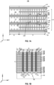
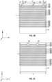
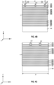
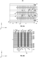
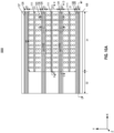
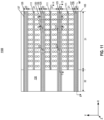
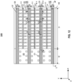
- FIG. 1A illustrates a plan view of an exemplary 3D memory device 150, according to some embodiments.
- FIG. 1B illustrates a cross-sectional view of the 3D memory device 150 shown in FIG. 1A along the A-B direction.
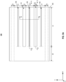
- FIG. 1C illustrates a cross-sectional view of the 3D memory device 150 shown in FIG. 1A along the C-D direction.
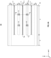
- 3D memory device 150 may be divided into a core region 31 and a staircase region 32, e.g., along the y-direction. Channel structures and support pillars can be formed in core region 31. Staircases and electric connection between conductor layers and outside circuits (e.g., contact plugs) can be formed in staircase region 32.
- Core region 31 may include one or more, e.g., a pair of, first source regions 23 extending along the x-direction.
- a first source structure may be formed in each first source region 23.
- a channel region 41 in which a plurality of channel structures and memory cells are formed, may be located between adjacent first source regions 23.
- channel region 41 may be divided into a plurality of block regions 21 by one or more second source regions 22 extending along the x-direction.
- a memory block may be formed in each block region 21, and a second source structure may be formed in each second source regions 22.
- 3D memory device 150 may include a substrate 100, a buffer oxide layer 101, and a stack structure 11 over buffer oxide layer 101.
- stack structure 11 may include a plurality of conductor layers and a plurality of insulating layers 104 interleaved over buffer oxide layer 101.
- the plurality of conductor layers may include a top conductor layer 129 having a plurality of top select conductor layers, a bottom conductor layer 128 having a plurality of bottom select conductor layers, and control conductor layers 127 between top conductor layer 129 and bottom conductor layer 128.
- Stack structure 11 may also include a dielectric cap layer 105 covering the plurality of conductor layers (i.e., 127-129) and insulating layers 104.
- stack structure 11 may also include a plurality of channel structures 140 extending from a top surface of dielectric cap layer 105 into substrate 100 along a vertical direction (e.g., the z-direction).
- Each channel structure 140 may include an epitaxial portion 115 at a bottom portion, a drain structure 120 at a top portion, and a semiconductor channel 119 between epitaxial portion 115 and drain structure 120.
- Semiconductor channel 119 may include a memory film 116, a semiconductor layer 117, and a dielectric core 118.
- Epitaxial portion 115 may contact and be conductively connected to substrate 100, and semiconductor channel 119 may contact and be conductively connected to drain structure 120 and epitaxial portion 115.
- a plurality of memory cells may be formed by semiconductor channels 119 and control conductor layers 127.
- stack structure 11 may include a plurality of contact plugs 131 in an insulator 130 and each in contact with a respective conductor layer (e.g., 127, 128, or 129) and a peripheral circuit (not shown). Contact plugs 131 may apply a word line voltage on the connected conductor layers.
- a first source structure may be formed in first source region 23 to extend along the x-direction in core region 31 and staircase region 32.
- the first source structure may include a source contact 126 in an insulating structure 137.
- a second source structure may be formed in second source region 22 to extend along the x-direction in core region 31 and staircase region 32.
- the second source structure may include a plurality of source contacts 125 each in a respective insulating structure 136. Source contacts 125 and respective insulating structures 136 formed in one second source region 22 (e.g., of the same second source structure) may be aligned along the x-direction.
- the first and second source structures may each extend vertically through stack structure 11 and contact substrate 100, applying a source voltage on the memory cells through substrate 100.
- 3D memory device 150 may include one or more support structures 152 aligned along the x-direction and dividing a second source structure into the plurality of source contacts 125 each in the respective insulating structure 136.
- support structure 152 includes a dividing structure 112 connecting adjacent memory blocks (or block regions 21) and a plurality of interleaved conductor portions (e.g., 127-0 and 128-0) and insulating portions 104-0 under dividing structure 112.
- Support structure 152 may provide support to 3D memory device 150 during the formation of the second source structures and conductor layers (e.g., 127-129).
- one or more cut structures 111 may be formed extending in parallel with the first source structures and the second source structures in channel region 41. Cut structures 111 may divide top conductor layer 129 into a plurality of top select conductor layers, functioning as top select gate electrodes.
- Substrate 100 can include silicon (e.g., single crystalline silicon), silicon germanium (SiGe), gallium arsenide (GaAs), germanium (Ge), silicon on insulator (SOI), germanium on insulator (GOI), or any other suitable materials.
- substrate 100 is a thinned substrate (e.g., a semiconductor layer), which was thinned by grinding, etching, chemical mechanical polishing (CMP), or any combination thereof.
- substrate 100 includes silicon.
- Channel structures 140 may form an array and may each extend vertically above substrate 100.
- Channel structure 140 may extend through a plurality of pairs each including a conductor layer (e.g., 127, 128, or 129) and an insulating layer 104 (referred to herein as "conductor/insulating layer pairs").
- buffer oxide layer 101 is formed between substrate 100 and stack structure 11.
- stack structure 11 can include a staircase structure, e.g., in staircase region 32.
- the number of the conductor/insulating layer pairs in stack structure 11 determines the number of memory cells in 3D memory device 150.
- conductor layers (e.g., 127-129) and insulating layers 104 in stack structure 11 are alternatingly arranged along the vertical direction in block regions 21.
- Conductor layers (e.g., 127-129) can include conductive materials including, but not limited to, tungsten (W), cobalt (Co), copper (Cu), aluminum (Al), polysilicon, doped silicon, silicides, or any combination thereof.
- Insulating layers 104 can include dielectric materials including, but not limited to, silicon oxide, silicon nitride, silicon oxynitride, or any combination thereof.
- buffer oxide layer 101 and dielectric cap layer 105 each includes a dielectric material such as silicon oxide.
- top conductor layer 129 includes a plurality of top select conductor layers, which function as the top select gate electrodes.
- Control conductor layers 127 may function as select gate electrodes and form memory cells with intersecting channel structures 140.
- bottom conductor layer 128 includes a plurality of bottom select conductor layers, which function as the bottom select gate electrodes. Top select gate electrodes and bottom select gate electrodes can respectively be applied with desired voltages to select a desired memory block/finger/page.
- channel structure 140 can include a semiconductor channel 119 extending vertically through stack structure 11.
- Semiconductor channel 119 can include a channel hole filled with a channel-forming structure, e.g., semiconductor materials (e.g., as a semiconductor layer 117) and dielectric materials (e.g., as a memory film 116).
- semiconductor layer 117 includes silicon, such as amorphous silicon, polysilicon, or single crystalline silicon.
- memory film 116 is a composite layer including a tunneling layer, a memory layer (also known as a "charge trap layer"), and a blocking layer.
- the remaining space of the channel hole of semiconductor channel 119 can be partially or fully filled with a dielectric core 118 including dielectric materials, such as silicon oxide.
- Semiconductor channel 119 can have a cylinder shape (e.g., a pillar shape).
- Dielectric core 118, semiconductor layer 117, the tunneling layer, the memory layer, and the blocking layer are arranged radially from the center toward the outer surface of the pillar in this order, according to some embodiments.
- the tunneling layer can include silicon oxide, silicon oxynitride, or any combination thereof.
- the memory layer can include silicon nitride, silicon oxynitride, silicon, or any combination thereof.
- the blocking layer can include silicon oxide, silicon oxynitride, high dielectric constant (high-k) dielectrics, or any combination thereof.
- the memory layer can include a composite layer of silicon oxide/silicon oxynitride (or silicon nitride)/silicon oxide (ONO).
- channel structure 140 further includes an epitaxial portion 115 (e.g., a semiconductor plug) in the lower portion (e.g., at the lower end of bottom) of channel structure 140.
- epitaxial portion 115 e.g., a semiconductor plug
- the "upper end" of a component is the end farther away from substrate 100 in the vertical direction
- the "lower end” of the component is the end closer to substrate 100 in the vertical direction when substrate 100 is positioned in the lowest plane of 3D memory device 150.
- Epitaxial portion 115 can include a semiconductor material, such as silicon, which is epitaxially grown from substrate 100 in any suitable directions.
- epitaxial portion 115 includes single crystalline silicon, the same material as substrate 100.
- epitaxial portion 115 can include an epitaxially-grown semiconductor layer grown from substrate 100.
- Epitaxial portion 115 can also include a different material than substrate 100.
- epitaxial portion 115 includes at least one of silicon, germanium, and silicon germanium.
- part of epitaxial portion 115 is above the top surface of substrate 100 and in contact with semiconductor channel 119.
- Epitaxial portion 115 may be conductively connected to semiconductor channel 119.
- a top surface of epitaxial portion 115 is located between a top surface and a bottom surface of a bottom insulating layer 104 (e.g., the insulating layer at the bottom of stack structure 11).
- channel structure 140 further includes drain structure 120 (e.g., channel plug) in the upper portion (e.g., at the upper end) of channel structure 140.
- Drain structure 120 can be in contact with the upper end of semiconductor channel 119 and may be conductively connected to semiconductor channel 119.
- Drain structure 120 can include semiconductor materials (e.g., polysilicon) or conductive materials (e.g., metals).
- drain structure includes an opening filled with Ti/TiN or Ta/TaN as an adhesion layer and tungsten as a conductor material. By covering the upper end of semiconductor channel 119 during the fabrication of 3D memory device 150, drain structure 120 can function as an etch stop layer to prevent etching of dielectrics filled in semiconductor channel 119, such as silicon oxide and silicon nitride.
- first source region 23 and second source region 22 may divide channel region 41 into a plurality of block regions 21, which can further be divided to form a plurality of memory fingers by one or more cut structures 111.
- a plurality of channel structures 140 e.g., memory cells
- first source regions 23, second source regions 22, and cut structures 111 may extend along the x-direction.
- cut structures 111 may extend along the x-direction in channel region 41, and first and second source regions 23 and 22 may extend laterally in core region 31 and staircase region 32.
- the number of cut structures 111 in a block region 21 may range from 0 to n, n being a suitable positive integer.
- the number of n should be determined based on the design and/or fabrication of 3D memory device 150 and should not be limited by the embodiments of the present disclosure. For illustrative purposes, n is equal to 1 in the present disclosure.
- cut structure 111 includes a suitable dielectric material, such as one or more of silicon oxide, silicon nitride, and silicon oxynitride, and divides the respective block region 21 (or memory block) into a pair of memory fingers. Specifically, cut structure 111 may extend vertically (e.g., along the z-direction) into the top insulating layer 104 (i.e., the insulating layer 104 under top conductor layer 129). In some embodiments, a bottom surface of cut structure 111 is between a top surface and a bottom surface of top insulating layer 104. In some embodiments, cut structure 111 divides top conductor layer 129 into a plurality of top select conductor layers. A voltage can be applied on one or more top select conductor layers to select a desired memory finger/page/block.
- a suitable dielectric material such as one or more of silicon oxide, silicon nitride, and silicon oxynitride
- a first source structure includes a source contact 126 in an insulating structure 137, extending along the x-direction.
- Source contact 126 may be in contact with and form a conductive connection with substrate 100 for applying a source voltage on memory cells.
- source contact 126 includes one or more of polysilicon, silicides, germanium, silicon germanium, copper, aluminum, cobalt, and tungsten.
- insulating structure 137 includes one or more of silicon oxide, silicon nitride, and silicon oxynitride.
- insulator 130 includes a suitable dielectric material such as silicon oxide, silicon nitride, and/or silicon oxynitride.
- contact plugs 131 are each in contact with and conductively connected to a respective conductor layer (e.g., 127, 128, or 129).
- Contact plugs 131 may include one or more of polysilicon, silicides, germanium, silicon germanium, copper, aluminum, cobalt, and tungsten.
- a second source structure includes a plurality of source contacts 125 each in a respective insulating structure 136.
- the materials of source contacts 125 and insulating structures 136 may be similar to or the same as source contacts 126 and insulating structures 137, and the description is thus not repeated herein.
- At least one support structure 152 may be formed between a pair of source contacts 125 (and a pair of insulating structures 136) and in contact with adjacent block regions 21 (or memory blocks). As shown in FIGs. 1B and 1C , support structure 152 may include a dividing structure 112 and a plurality of interleaved conductor portions (e.g., 127-0 and 128-0) and insulating portions 104-0 under dividing structure 112.
- Conductor portions (e.g., 127-0 and 128-0) and insulating portions 104-0 may respectively be in contact with (e.g., connected to) conductor layers (e.g., 127 and 128) and insulating layers 104 of the same level in adjacent block regions 21 (or memory blocks) along the y-direction.
- conductor portions (e.g., 127-0 and 128-0) and insulating portions 104-0 are disconnected from conductor layers (e.g., 127 and 128) and insulating layers 104 of any block regions 21 (or memory blocks) in respective second source region 22 along the x-direction.
- 3D memory device 150 includes a plurality of support structures 152 aligned along the x-direction to divide the second source structure into a plurality of source contacts 125, each in the respective insulating structure 136. As shown in FIGs. 1A-1C , the plurality of support structures 152 divides the second source structure into a plurality of disconnected source contacts 125 and insulating structures 136 along the x-direction. The plurality of support structures 152 may also connect conductor layers (e.g., 127 and 128) and insulating layers 104 of adjacent block regions 21 along the y-direction. In some embodiments, support structures 152 may be formed in channel region 41.
- dividing structure 112 includes a suitable material that has sufficient stiffness and strength and can be used as an etch mask for the formation of slit structure before the formation of second source structure.
- the material of dividing structure 112 may also sustain the gate replacement process for the formation of conductor layers (e.g., 127-129) and conductor portions (e.g., 127-0 and 128-0).
- dividing structure 112 includes one or more of silicon oxide, silicon nitride, and/or silicon oxynitride.
- dividing structure 112 and cut structure 111 may include the same material, e.g., silicon oxide.
- conductor portions (e.g., 127-0 and 128-0) and insulating portions 104-0 may include the same material as respective conductor layers (e.g., 127 and 128) and insulating layers 104 of the same level in adjacent block regions 21 (or memory blocks).
- a bottom surface of dividing structure 112 is between a top surface and a bottom surface of top insulating layer 104.
- a depth of dividing structure 112 and a depth of cut structure 111 may be the same along the z-axis, e.g., from the top surface of dielectric cap layer 145 to a same level in top insulating layer 104.
- a width of dividing structure 112 along the y-direction may be equal to or greater than the width of second source structure along the y-direction.
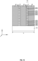
- FIG. 13B illustrates an enlarged plan view 1320 of dividing structure 112, adjacent source contacts 125, and adjacent insulating structures 136. As shown in FIG. 13B , a width d2 of dividing structure 112 along the y-direction is equal to or greater than a width d1 of second source structure (or insulating structure 136) along the y-direction. In some embodiments, d2 is greater than d1.
- d2 being equal to or greater than d1 prevents support structure 152 (or interleaved conductor portions (e.g., 127-0 and 128-0) and insulating portions 104-0) from being disconnected from adjacent memory blocks. Details are described as follows.
- 3D memory device 150 can be part of a monolithic 3D memory device.
- monolithic means that the components (e.g., the peripheral device and memory array device) of the 3D memory device are formed on a single substrate.
- the fabrication encounters additional restrictions due to the convolution of the peripheral device processing and the memory array device processing.
- the fabrication of the memory array device e.g., NAND channel structures
- 3D memory device 150 can be part of a non-monolithic 3D memory device, in which components (e.g., the peripheral device and memory array device) can be formed separately on different substrates and then bonded, for example, in a face-to-face manner.
- the memory array device substrate e.g., substrate 102
- the peripheral device e.g., including any suitable digital, analog, and/or mixed-signal peripheral circuits used for facilitating the operation of 3D memory device 150, such as page buffers, decoders, and latches; not shown
- the memory array device e.g., NAND memory strings
- the memory array device substrate (e.g., substrate 100) is flipped and faces down toward the peripheral device (not shown) for hybrid bonding, so that in the bonded non-monolithic 3D memory device, the memory array device is above the peripheral device.
- the memory array device substrate (e.g., substrate 100) can be a thinned substrate (which is not the substrate of the bonded non-monolithic 3D memory device), and the back-end-of-line (BEOL) interconnects of the non-monolithic 3D memory device can be formed on the backside of the thinned memory array device substrate.
- FIGs. 2-4 , 7 , and 9-12 illustrate a fabrication process to form 3D memory device 150
- FIG. 14A illustrates a flowchart 1400 of the fabrication process, according to some embodiments.
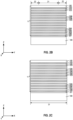
- FIGs. 2A-2D illustrate a corresponding structure 200.
- a stack structure 11 having a dielectric stack of interleaved initial insulating layers 104i and initial sacrificial layers 103i is formed over a substrate 100.
- Initial sacrificial layers 103i may be used for subsequent formation of control conductor layers 127.
- Stack structure 11 may also include a top initial sacrificial layer 106i and a bottom initial sacrificial layer 105i respectively for subsequent formation of top conductor layer 129 and bottom conductor layer 128.
- stack structure 11 includes a dielectric cap layer 145 over initial sacrificial layers (e.g., 103i, 105i, and 106i) and initial insulating layers 104i.
- 3D memory device 150 may include a core region 31 for forming channel structures 140 and support pillars (not shown), and a staircase region 32 for forming staircases and contact plugs (e.g., 131) on the staircases.
- Core region 31 may include a channel region 41 for forming channel structures 140.
- channel region 41 may be between first source regions 23.
- One or more second source regions 22 may subsequently be formed between first source regions 23, and block regions 21 may each be located between first source region 23 and second source region 22 or between second source regions 22.
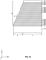
- Stack structure 11 may have a staircase structure, as shown in FIG. 2D .
- the staircase structure can be formed by repetitively etching a material stack that includes a plurality of interleaved sacrificial material layers and insulating material layers using an etch mask, e.g., a patterned PR layer over the material stack.
- the interleaved sacrificial material layers and the insulating material layers can be formed by alternatingly depositing layers of sacrificial material and layers of insulating material over buffer oxide layer 101 until a desired number of layers is reached.
- a sacrificial material layer is deposited over buffer oxide layer 101, and an insulating material layer is deposited over the sacrificial material layer, so on and so forth.
- the sacrificial material layers and insulating material layers can have the same or different thicknesses.
- a sacrificial material layer and the underlying insulating material layer are referred to as a dielectric pair 107.
- one or more dielectric pairs 107 can form one level/staircase.
- the PR layer is trimmed (e.g., etched incrementally and inwardly from the boundary of the material stack, often from all directions) and used as the etch mask for etching the exposed portion of the material stack.
- the amount of trimmed PR can be directly related (e.g., determinant) to the dimensions of the staircases.
- the trimming of the PR layer can be obtained using a suitable etch, e.g., an isotropic dry etch such as a wet etch.
- One or more PR layers can be formed and trimmed consecutively for the formation of the staircase structure.
- Each dielectric pair 107 can be etched, after the trimming of the PR layer, using suitable etchants to remove a portion of both the sacrificial material layer and the underlying insulating material layer.
- the etched sacrificial material layers and insulating material layers may form initial sacrificial layers (e.g., 103i, 105i, and 106i) and initial insulating layers 104i.
- the PR layer can then be removed.
- the insulating material layers and sacrificial material layers may have different etching selectivities during the subsequent gate-replacement process.
- the insulating material layers and the sacrificial material layers include different materials.
- the insulating material layers include silicon oxide, and the deposition of insulating material layers include one or more of chemical vapor deposition (CVD), atomic layer deposition (ALD), physical vapor deposition (PVD), and sputtering.
- the sacrificial material layers include silicon nitride, and the deposition of insulating material layers include one or more of CVD, PVD, ALD, and sputtering.
- the etching of the sacrificial material layers and the insulating material layers include one or more suitable anisotropic etching process, e.g., dry etch.
- a plurality of support openings are formed to be aligned along a lateral direction, a length of the support opening being less than a length of the source structure (Operation 1404).
- a cut opening is formed extending along the lateral direction.
- FIGs. 3A-3D illustrate a corresponding structure 300.
- At least one support opening 109 is formed in second source region 22.
- a plurality of support openings 109 are formed in each second source region 22 along the x-direction, separated from one another.
- a length of support opening 109 may be less than a length of the second source structure to be formed (or the length of second source region 22 or the slit structure in which the second source structure is formed).
- the plurality of support openings 109 may have the same or different dimensions.
- the plurality of support openings 109 may have the same shapes and dimensions along the x-y plane, and same depth along the z-direction.
- a width of support opening 109 may be greater than or equal to a width of second source region 22.
- a bottom surface of support opening 109 may be between a top surface and a bottom surface of top initial insulating layer 104i (e.g., the initial insulating layer 104i under top initial sacrificial layer 106i).
- a suitable patterning process e.g., an etching process, such as a dry etch and/or wet etch, may be performed to form support openings 109.
- one or more cut openings 108 may be formed extending along the x-direction by the same patterning/etching process that form support openings 110.
- a length of cut opening 108 may be the same as a length of channel region 41 (e.g., or core region 31) along the x-direction.
- One or more cut openings 108 may be formed in one block region 21, depending on, e.g., the number of memory fingers to be formed in a memory block.
- a bottom surface of cut opening 108 may be between a top surface and a bottom surface of top initial insulating layer 104i (e.g., the initial insulating layer 104i under top initial sacrificial layer 106i).
- a depth of support opening 109 is the same as a depth of cut opening 108 along the vertical direction, e.g., the bottom surfaces of support opening 109 and cut opening 108 being on the same level of top initial insulating layer 104i.
- the support openings are filled with a dielectric material to form the dividing structures that connect adjacent block regions (Operation 1406).
- any cut opening is filled with the dielectric material to form a cut structure in the respective block region.
- FIGs. 4A-4D illustrate a corresponding structure 400.
- support openings 109 may be filled with a suitable material to form dividing structures 112.
- Dividing structures 112 may have sufficient stiffness and strength to function as an etch mask for the formation of slit structures before the formation of second source structures.
- Dividing structure 112 may also sustain the gate replacement process for the formation of conductor layers (e.g., 127-129) and conductor portions (e.g., 127-0 and 128-0).
- dividing structure 112 may include a different material than the sacrificial layers so that dividing structure 112 has little or no damages during the gate-replacement process in which the sacrificial layers are etched away.
- dividing structure 112 includes one or more of silicon oxide, silicon nitride, and/or silicon oxynitride.
- Dividing structure 112 can be deposited by a suitable deposition process such as CVD, ALD, PVD, sputtering, or a combination thereof.
- cut openings 108 may be filled with the same material that fills support opening 109, using the same deposition process.
- Cut structures 111 may be formed extending along the x-direction.
- FIGs. 7A and 7B illustrate a corresponding structure 700.
- a plurality of channel structures 140 can be formed in channel region 41, e.g., in each block region 21.
- a plurality of channel holes may be formed extending vertically through stack structure 11.
- a plurality of channel holes are formed through the interleaved initial sacrificial layers (103i, 105i, and 106i) and initial insulating layers 104i.
- the plurality of channel holes may be formed by performing an anisotropic etching process, using an etch mask such as a patterned PR layer, to remove portions of stack structure 11 and expose substrate 100.
- at least one channel hole is formed on each side of dividing structures 112 along the y-direction.
- a plurality of channel holes are formed in each block region 21.
- a recess region may be formed at the bottom of each channel hole to expose a top portion of substrate 100 by the same etching process that forms the channel hole above substrate 100 and/or by a separate recess etching process.
- a semiconductor plug is formed at the bottom of each channel hole, e.g., over the recess region.
- the semiconductor plug may be formed by an epitaxial growth process and/or a deposition process.
- the semiconductor plug is formed by epitaxial growth and is referred to as epitaxial portion 115.
- a recess etch (e.g., dry etch and/or wet etch) may be performed to remove excess semiconductor material on the sidewall of the channel hole and/or control the top surface of epitaxial portion 115 at a desired position.
- the top surface of epitaxial portion 115 is located between the top and bottom surfaces of the bottom initial insulating layer 104i.
- the channel holes are formed by performing a suitable etching process, e.g., an anisotropic etching process (e.g., dry etch) and/or an isotropic etching process (wet etch).
- epitaxial portion 115 includes single crystalline silicon is formed by epitaxially grown from substrate 100.
- epitaxial portion 115 includes polysilicon formed by a deposition process.
- the formation of epitaxially-grown epitaxial portion 115 can include, but not limited to, vapor-phase epitaxy (VPE), liquid-phase epitaxy (LPE), molecular-beam epitaxy (MPE), or any combinations thereof.
- the formation of deposited epitaxial portion 115 may include, but not limited by, CVD, PVD, and/or ALD.
- a semiconductor channel 119 is formed over and contacting epitaxial portion 115 in the channel hole.
- Semiconductor channel can include a channel-forming structure that has a memory film 116 (e.g., including a blocking layer, a memory layer, and a tunneling layer), a semiconductor layer 117 formed above and connecting epitaxial portion 115, and a dielectric core 118 filling up the rest of the channel hole.
- memory film 116 is first deposited to cover the sidewall of the channel hole and the top surface of epitaxial portion 115, and semiconductor layer 117 is then deposited over memory film 116 and above epitaxial portion 115.
- the blocking layer, memory layer, and tunneling layer can be subsequently deposited in this order using one or more thin film deposition processes, such as ALD, CVD, PVD, any other suitable processes, or any combination thereof, to form memory film 116.
- Semiconductor layer 117 can then be deposited on the tunneling layer using one or more thin film deposition processes, such as ALD, CVD, PVD, any other suitable processes, or any combination thereof.
- dielectric core 118 is filled in the remaining space of the channel hole by depositing dielectric materials after the deposition of semiconductor layer 117, such as silicon oxide.
- drain structure 120 is formed in the upper portion of each channel hole.
- parts of memory film 116, semiconductor layer 117, and dielectric core 118 on the top surface of stack structure 11 and in the upper portion of each channel hole can be removed by CMP, grinding, wet etching, and/or dry etching to form a recess in the upper portion of the channel hole so that a top surface of semiconductor channel may be between the top surface and the bottom surface of dielectric cap layer 105.
- Drain structure 120 then can be formed by depositing conductive materials, such as metals, into the recess by one or more thin film deposition processes, such as CVD, PVD, ALD, electroplating, electroless plating, or any combination thereof.
- a channel structure 140 is thereby formed.
- a plurality of memory cells may subsequently be formed by the intersection of semiconductor channels 119 and control conductor layers 127.
- a planarization process e.g., dry/wet etch and/or CMP, is performed to remove any excess material on the top surface of stack structure 11.
- the plurality of dividing structures may be used as an etch mask to form a slit structure with a plurality of slit openings divided by the plurality of dividing structures (Operation 1410).
- FIGs. 9A-9E illustrate a corresponding structure 900.
- a slit structure 123 having a plurality of slit openings, may be formed in second source region 22 extending along the x-direction. Along the x-direction, adjacent slit openings may be separated by a dividing structure 112 and the remaining portion of stack structure 11 covered by and under dividing structure 112. The slit openings may extend vertically through stack structure 11 and expose substrate 100.
- the patterned/etched initial sacrificial layers form a plurality of sacrificial layers in block regions 21 and a plurality of sacrificial portions covered by and under dividing structure 112.
- Each sacrificial portion may be in contact with, e.g., connected to, sacrificial layers of the same level in adjacent block regions 21 along the y-direction.
- the patterned/etched initial insulating layers form a plurality of insulating layers 104 in block regions 21 and a plurality of insulating portions 104-0 covered by and under dividing structure 112.
- Each insulating portion 104-0 may be in contact with, e.g., connected to, insulating layers 104 of the same level in adjacent block regions 21 along the y-direction.
- the plurality of insulating portions 104-0 and the plurality of sacrificial portions may be interleaved with one another extending from under a respective dividing structure 112 to substrate 100.
- a width of dividing structure 112 along the y-direction may be equal to or greater than the width of the respective slit structure 123 (e.g., adjacent slit openings) along the y-direction.
- FIG. 13A illustrates an enlarged plan view 1310 of dividing structure 112 and adjacent slit openings. As shown in FIG. 13A , a width d2 of dividing structure 112 along the y-direction is equal to or greater than a width d1 of slit structure 123 along the y-direction.
- d2 is greater than d1.
- d2 being equal to or greater than d1 prevents the interleaved sacrificial portions and insulating portions 104-0 from being disconnected from adjacent block regions 21 during the formation of slit structure 123. That is, dividing structures 112 may keep adjacent memory blocks connected through the interleaved sacrificial portions and insulating portions 104-0 during the formation of slit structure 123.
- dividing structures 112 is used as an etch mask and an anisotropic etching process, e.g., dry etch, is performed to remove portions of stack structure 11 in second source region 22 to form slit structure 123.
- the remaining portions of stack structure 11 in second source region 22 may form the interleaved sacrificial portions and insulating portions.
- Dividing structure 112 and underlying interleaved sacrificial portions and insulating portions 104-0 may form an initial support structure.
- one or more other slit structures 124 may be formed in first source regions 23 by the same patterning/etching process that forms slit openings of slit structure 123.
- Each other slit structure 124 e.g., having a single slit opening, may extend along the x-direction and through stack structure 11 to expose substrate 100.
- other slit structures 124 may extend in core region 31 and staircase region 32.
- FIG. 9A-9E illustrate a corresponding structure.
- sacrificial layers in block regions 21 and sacrificial portions retained in second source regions 22 may be removed to form a plurality of lateral recesses, and a suitable conductor material may be deposited to fill up the lateral recesses, forming a plurality of conductor layers (e.g., 127-129) in block regions 21 and a plurality of conductor portions (e.g., 127-0 and 128-0) in second source regions 22.
- a support structure 152 having dividing structure 112 and underlying interleaved conductor portions (e.g., 127-0 and 128-0) and insulating portions 104-0 may be formed.
- Control conductor layers 127 may intersect with semiconductor channels 119 and form a plurality of memory cells in each block region 21, which forms a memory block.
- the top sacrificial layer in block regions 21 may form a top conductor layer 129, and the bottom sacrificial layer in block regions 21 may form a bottom conductor layer 128.
- the initial support structure can form a support structure 152.
- the conductor material may include one or more of tungsten, aluminum, copper, cobalt, silicides, and polysilicon.
- a suitable isotropic etching process e.g., wet etch, can be performed to remove sacrificial layers and sacrificial portions, and form the plurality of lateral recesses.
- a suitable deposition process such as CVD, PVD, ALD, and/or sputtering can be performed to deposit the conductor material into the lateral recesses to form conductor layers (e.g., 127-129) and conductor portions (e.g., 127-0 and 128-0).
- FIGs. 10A-10E illustrate a corresponding structure 1000.
- an insulating structure 136 may be formed in each slit opening of slit structure 123, and a source contact 125 may be formed in the respective insulating structure 136.
- the insulating structures 136 and the source contacts 125 in each second source region 22 may form a second source structure.
- An insulating structure 137 may be formed in each other slit structure 124, and a source contact 126 may be formed in each other slit structure 124.
- the insulating structure 137 and respective source contact 126 may form a first source structure.
- Support structure 152 may separate adjacent source contacts 125 and insulating structures 136 along the x-direction, and may connect adjacent memory blocks along the y-direction.
- insulating structures 136 and 137 includes silicon oxide, and is deposited by one or more of CVD, PVD, ALD, and sputtering. A recess etch may be performed to remove portions of insulating structures 136 and 137 at the bottom of the respective slit structure to expose substrate 100.
- source contacts 125 and 126 each includes one or more of tungsten, aluminum, copper, cobalt, silicides, and polysilicon, and a suitable deposition process, e.g., one or more of CVD, PVD, ALD, and sputtering, is performed to deposit source contacts 125 and 126 into respective slit structures.
- an insulator is formed in the staircase region and one or more contact plugs are formed in the insulator to contact the conductor layers (Operation 1416).
- FIGs. 11 and 12 illustrate corresponding structures 1100 and 1200.
- an insulator 130 can be formed in staircase region 32 to cover the staircases (e.g., conductor layers 127-129) and insulate contact plugs 131 from one another.
- One or more contact plugs 131 are formed in insulator 130 to contact and form an conductive connection with conductor layers 127-129.
- insulator 130 includes silicon oxide and is deposited by one or more of CVD, PVD, ALD, and sputtering.
- a suitable anisotropic etching process e.g., dry etch, can be performed to form one or more plug openings through insulator 130 and expose one or more conductor layers (e.g., 127, 128, and/or 129).
- a suitable conductive material such as tungsten is deposited to fill up the plug openings.
- at least one contact plug is formed on one conductor layer (e.g., 127, 128, and/or 129).
- a planarization process e.g., CMP and/or recess etch, is performed to remove any excess material, e.g., from the formation of various structures, over stack structure 11.
- FIGs. 2 , 5 , 6 and 8-12 illustrates another fabrication process to form 3D memory device 150
- FIG. 14B illustrates a flowchart 1450 of the fabrication process, according to some embodiments.
- one or more initial dividing structures are formed and etched to form one or more dividing structures.
- same or similar operations illustrated in FIGs. 2-4 , 7 , and 9-12 are not repeated in the description.
- FIGs. 2A-2D illustrate a corresponding structure 200.
- the description of the fabrication process and structure 200 can be referred to the description of Operation 1402 and is not repeated herein.
- a support opening can be formed extending along a lateral direction, a length of the support opening being equal to a length of the source structure (Operation 1454).
- a cut opening is formed extending along the lateral direction.
- FIGs. 5A-5C illustrate a corresponding structure 500.
- a support opening 110 is formed in second source region 22.
- a length of support opening 110 may be equal to a length of the second source structure to be formed (or the length of second source region 22 or the slit structure in which the second source structure is formed).
- a width of support opening 109 may be greater than or equal to a width of second source region 22.
- a bottom surface of support opening 110 may be between a top surface and a bottom surface of first initial insulating layer 104i (e.g., the initial insulating layer 104i) under top initial sacrificial layer 106i.
- one or more cut openings 108 are formed in a block region 21.
- the fabrication of support opening 110 and any cut opening 108 can be referred to the fabrication of support openings 109 and cut openings 108 described in FIGs. 3A-3D and is not repeated herein.
- a depth of support opening 110 is the same as a depth of cut opening 108 along the vertical direction, e.g., the bottom surfaces of support opening 110 and cut opening 108 being on the same level of top initial insulating layer 104i.
- the support opening is filled with a dielectric material to form an initial dividing structure connecting adjacent block regions (Operation 1456).
- any cut opening is filled with the dielectric material to form a cut structure in the block region.
- FIGs. 6A-6C illustrate a corresponding structure 600.
- a dielectric material can be deposited to fill up support opening 110 and form an initial dividing structure 113.
- initial dividing structure 113 is located between adjacent block regions 21.
- a length of initial dividing structure 113 is equal to the length of the second source structure or slit structure to be formed. Any cut opening can be filled with the dielectric material to form a cut structure 111 in the respective block region.
- the deposition of dielectric material to form initial dividing structure 113 and any cut structure 111 can be referred to the formation of dividing structure 112 and cut structure 111 described in FIGs. 4A-4C and is not repeated herein.
- FIGs. 8A and 8B illustrate a corresponding structure 800.
- a plurality of channel structures 140 can be formed in channel region 41.
- at least one channel structure 140 is formed on each side of initial dividing structure 113 along the y-direction.
- a plurality of channel structures 140 are formed in each block regions 21. The formation of channel structures 140 can be referred to the formation of channel structures 140 described in FIGs. 7A and 7B and is not repeated herein.
- an initial support structure having a dividing structure is formed (Operation 1460). Portions of the initial dividing structure can be removed to form a dividing structure, and the dividing structure can be used as an etch mask to remove portions of the stack structure and form the initial support structure.
- FIGs. 9A-9E illustrate a corresponding structure 900.
- portions of initial dividing structure 113 can be removed to form one or more dividing structure 112 arranged along the x-direction and expose portions of stack structure 11.
- top initial insulating layer 104i is exposed.
- the dividing structures 112 can be used as an etch mask to remove portions of stack structure 11 exposed in second source region 22 to form a slit structure 123 with a plurality of disconnected slit openings that expose substrate 100.
- Initial dividing structure 113 and stack structure 11 can be patterned/etched using the same patterning/etching process or separate patterning/etching processes.
- initial dividing structure 113 may first be patterned to form dividing structures 112, and a different etching process can be performed to remove exposed portions of stack structure 11, and form slit openings of slit structure 123 and one or more initial support structures.
- initial dividing structure 113 and portions of stack structure 11 under initial dividing structure 113 can be patterned using the same etching process to form slit openings of slit structure 123 and one or more initial support structures.
- initial dividing structure 113 and stack structure 11 are patterned using the same etching process to reduce the steps and time of the patterning operation.
- Initi1al dividing structure 113 and stack structure 11 can be patterned/etched using one or more suitable etching processes, e.g., dry etch and/or wet etch. Details of the initial support structures can be referred to the description of initial support structures described in FIGs. 9A-9E of flowchart 1400 and are not repeated herein.
- FIG. 14B a plurality of conductor layers, a plurality of memory blocks, and a support structure are formed (Operation 1462) and a source structure is formed in each slit structure (Operation 1464). An insulator and contact plugs are formed in the staircase region (Operation 1466).
- FIGs. 9-12 illustrate corresponding structures 900-1200. Detailed descriptions of Operations 1462-1466 can be referred to the description of Operations 1412-1416 and are not repeated herein.
Landscapes
- Semiconductor Memories (AREA)
- Non-Volatile Memory (AREA)
Claims (9)
- Dispositif de mémoire tridimensionnelle (3D), comprenant:un empilement de mémoire comprenant une pluralité de couches conductrices (127-129) et une pluralité de couches isolantes (104) entrelacées s'étendant latéralement dans l'empilement de mémoire;une pluralité de structures de canaux (140) s'étendant verticalement à travers l'empilement de mémoire dans le substrat (100), la pluralité de structures de canaux (140) et la pluralité de couches conductrices se chevauchant mutuellement et formant une pluralité de cellules de mémoire;au moins une structure de fente (123, 124) s'étendant verticalement et latéralement dans l'empilement de mémoire et divisant la pluralité de cellules de mémoire en au moins un bloc de mémoire, ladite au moins une structure de fente (123, 124) comprenant chacune une pluralité d'ouvertures de fente et une structure de support (152) entre des ouvertures de fente adjacentes, la structure de support (152) étant en contact avec des blocs de mémoire adjacents et en contact avec le substrat (100); etune structure de source comprenant une entretoise isolante (136, 137) dans chacune de la pluralité d'ouvertures de fente, etun contact de source (125, 126) dans l'entretoise isolante respective,la structure de support (152) s'étendant verticalement à travers l'empilement de mémoire vers le substrat (100) et étant isolée des contacts de source adjacents (125, 126) par des entretoises isolantes respectives des contacts de source adjacents (125, 126),la structure de support (125) comprenant une structure de division (112);la structure de division (112) s'étendant latéralement pour connecter les blocs de mémoire adjacents; etla pluralité de parties conductrices (127-0) et la pluralité de parties isolantes (104-0) entrelacées étant chacune en contact avec des couches conductrices correspondantes et des couches isolantes correspondantes du même niveau de blocs de mémoire adjacents,caractérisé en ce quela structure de division (112) s'étend verticalement dans une première couche isolante (104i) de l'empilement de mémoire, la structure de division (112) se trouve au-dessus d'une pluralité de parties conductrices (172-0) et d'une pluralité de parties isolantes (104-0) entrelacées, etune face inférieure de la structure de division (112) est située entre une face supérieure et une face inférieure de la couche isolante supérieure (104), la structure de support (152) divisant la structure de source en une pluralité de contacts de source non connectés (125, 126), chacun dans l'entretoise isolant respective (136, 137),une largeur (d2) de la structure de division (112) le long d'une autre direction latérale perpendiculaire à la direction latérale dans laquelle s'étend ladite au moins une structure de fente étant supérieure à une largeur (d1) de chacune des ouvertures de fente adjacentes le long de ladite autre direction latérale.
- Dispositif de mémoire 3D selon la revendication 1, dans lequel la structure de division (112) comprend au moins un élément parmi l'oxyde de silicium, le nitrure de silicium ou l'oxynitrure de silicium.
- Dispositif de mémoire 3D selon la revendication 2, dans lequel la pluralité de parties conductrices (127-0) comprend au moins un élément parmi le tungstène, l'aluminium, le cuivre, le cobalt, les siliciures ou le polysilicium; et
la pluralité de parties isolantes (104-0) comprend au moins un élément parmi l'oxyde de silicium, le nitrure de silicium ou l'oxynitrure de silicium. - Dispositif de mémoire 3D selon la revendication 3, dans lequel la pluralité de parties conductrices (127-0) et les couches conductrices de blocs de mémoire adjacents sont constituées d'un même matériau; et
la pluralité de parties isolantes (104-0) et les couches isolantes de blocs de mémoire adjacents sont constituées d'un même matériau. - Dispositif de mémoire 3D selon la revendication 3, comprenant en outre une structure de coupe (111) qui s'étend latéralement et verticalement parallèlement à la structure de fente (123, 124) dans ledit au moins un bloc de mémoire et qui divise ledit au moins un bloc de mémoire en une pluralité de doigts de mémoire, dans lequel la structure de coupe (111) s'étend verticalement dans la première couche isolante de l'empilement de mémoire et contient au moins un élément parmi l'oxyde de silicium, le nitrure de silicium ou l'oxynitrure de silicium, une profondeur de la structure de coupe (111) étant la même qu'une profondeur de la structure de division (112) .
- Procédé de formation d'un dispositif de mémoire tridimensionnelle (3D), comprenant:former un empilement diélectrique comprenant une pluralité de couches isolantes initiales (104i) et une pluralité de couches sacrificielles initiales (103i, 106i) entrelacées sur un substrat (100);former au moins une structure de fente (123, 124) s'étendant verticalement et latéralement dans l'empilement diélectrique et divisant l'empilement diélectrique en une pluralité de régions de bloc (21), ladite au moins une structure de fente (123, 124) comprenant chacune une pluralité d'ouvertures de fente exposant le substrat (100) et une première structure de support (152) entre des structures de fente adjacentes,chacune des multiples parties de bloc (21) comprenant une pluralité de couches isolantes (104) et une pluralité de couches sacrificielles (103, 106) entrelacées; etla structure de support initiale (152) comprenant une pluralité de parties isolantes (104-0) et de parties sacrificielles entrelacées, chacune de la pluralité de parties isolantes (104-0) et de parties sacrificielles étant en contact avec des couches isolantes et des couches sacrificielles respectives (103, 106) du même niveau de parties de blocs adjacentes (21);former une pluralité de structures de canaux (140) s'étendant verticalement à travers l'empilement diélectrique;remplacer la pluralité de couches sacrificielles (103, 106) et la pluralité de parties sacrificielles par une pluralité de couches conductrices (127-129) et une pluralité de parties conductrices (127-0) par au moins une structure de fente (123, 124); etformer une structure de source dans chaque structure de fente (123, 124), comprenant une entretoise isolante dans chacune de la pluralité d'ouvertures de fente et un contact de source (125, 126) dans une entretoise isolante respective,la formation de ladite au moins une structure de fente (123, 124) comprenant:structurer l'empilement diélectrique pour former une ouverture de support (109, 110) le long d'une direction latérale dans laquelle s'étend la structure de fente respective (123, 124), une longueur de l'ouverture de support (109, 110) étant inférieure à une longueur de la structure de fente (123, 124) le long de la direction latérale, un fond de l'ouverture de support (109, 110) étant situé entre une surface supérieure et une surface inférieure d'une première couche isolante initiale de l'empilement diélectrique; etdéposer un matériau diélectrique pour remplir l'ouverture de support (109, 110) et former une structure de division (112), la structure de support (152) divisant la structure de source en une pluralité de contacts de source non connectés (125, 126), chacun dans l'entretoise isolant concerné (136, 137) le long d'une direction x,une largeur (d2) de la structure de division (112) le long d'une autre direction latérale perpendiculaire à la direction latérale le long de laquelle s'étend ladite au moins une structure de fente étant supérieure à une largeur de chacune des ouvertures de fente adjacentes le long de l'autre direction latérale,la formation de ladite au moins une structure de fente (123, 124) comprenant l'élimination de parties de l'empilement diélectrique adjacentes à la structure de division (112) le long de la direction latérale pour former une paire d'ouvertures de fente exposant le substrat (100), une largeur de la paire d'ouvertures de fente étant inférieure ou égale à une largeur de la structure de division (112) le long d'une autre direction latérale perpendiculaire à la direction latérale; etla structure de division (112) et les parties sacrificielles et isolantes entrelacées restantes (104-0) sous la structure de division (112) formant la structure de support initiale (152),l'élimination des parties de l'empilement diélectrique comprenant l'utilisation de la structure de division (112) comme masque de gravure pour graver les parties de l'empilement diélectrique adjacentes à la structure de division (112) et laisser les parties sacrificielles et les parties isolantes (104-0) entrelacées sous la structure de division (112).
- Procédé selon la revendication 6,
dans lequel la formation de ladite au moins une structure de fente (123, 124) comprend:structurer l'empilement diélectrique pour former une ouverture de support (109, 110) le long d'une direction latérale dans laquelle s'étend la structure de fente respective (123, 124), une longueur de l'ouverture de support (109, 110) étant égale à une longueur de la structure de fente (123, 124) de la direction latérale, un fond de l'ouverture de support (109, 110) étant situé entre une surface supérieure et une surface inférieure d'une première couche isolante initiale de l'empilement diélectrique; etdéposer un matériau diélectrique pour remplir l'ouverture de support (109, 110) et former une structure de division initiale (112i). - Procédé selon la revendication 7,
dans lequel la formation de ladite au moins une structure de fente (123, 124) comprend en outre:l'enlèvement d'une paire de secondes parties adjacentes à une première partie pour exposer des parties de l'empilement diélectrique sous les secondes parties le long de la direction latérale de la structure de division initiale (112i); etl'enlèvement des parties exposées de l'empilement diélectrique pour exposer le substrat (100) et former une paire d'ouvertures de fente, une largeur de chacune de la paire d'ouvertures de fente étant inférieure ou égale à une largeur de la structure de division initiale (112i) le long d'une autre direction latérale perpendiculaire à la direction latérale, une première partie restante de la structure de division initiale (112i) formant une structure de division (112), la structure de division (112) et les parties sacrificielles et les parties isolantes entrelacées restantes (104-0) sous la structure de division (112) formant la structure de support initiale (152), de préférence l'élimination des parties exposées de l'empilement diélectrique comprenant l'utilisation de la structure de division (112) comme masque de gravure pour graver les parties de l'empilement diélectrique adjacentes à la structure de division (112) et maintenir des parties conductrices (127-0) et des parties isolantes (104-0) entrelacées sous la structure de division (112). - Procédé selon l'une quelconque des revendications 6 à 8, comprenant en outre la formation d'une structure de coupe (111) dans au moins une de la pluralité de parties de bloc (21), la structure de découpe s'étendant parallèlement à ladite au moins une structure de fente (123, 124) et divisant ledit au moins un de la pluralité de blocs de mémoire en une pluralité de doigts,
dans lequel la formation de la structure de coupe (111) comprend:former une ouverture de coupe (108) dans ladite au moins une de la pluralité de parties de bloc (21) dans le même processus de structuration qui forme l'ouverture de support, l'ouverture de coupe (108) s'étendant parallèlement à ladite au moins une structure de fente (123, 124), une surface inférieure de l'ouverture de coupe (108) étant située entre une surface supérieure et une surface inférieure de la première couche isolante initiale; etdéposer un matériau diélectrique pour remplir l'ouverture de coupe (108) dans le même processus de dépôt que celui qui remplit l'ouverture de support (109, 110), formant ainsi la structure de coupe (111).
Priority Applications (1)
| Application Number | Priority Date | Filing Date | Title |
|---|---|---|---|
| EP24207287.4A EP4472380A3 (fr) | 2019-06-17 | 2019-08-23 | Dispositif de mémoire tridimensionnelle avec structures de support dans des fentes de ligne de grille et ses procédés de formation |
Applications Claiming Priority (2)
| Application Number | Priority Date | Filing Date | Title |
|---|---|---|---|
| CN201910522007.2A CN110176461B (zh) | 2019-06-17 | 2019-06-17 | 3d nand存储器及其形成方法 |
| PCT/CN2019/102121 WO2020252894A1 (fr) | 2019-06-17 | 2019-08-23 | Dispositif de mémoire tridimensionnel doté de structures de support dans des fentes de ligne de grille et leurs procédés de formation |
Related Child Applications (2)
| Application Number | Title | Priority Date | Filing Date |
|---|---|---|---|
| EP24207287.4A Division EP4472380A3 (fr) | 2019-06-17 | 2019-08-23 | Dispositif de mémoire tridimensionnelle avec structures de support dans des fentes de ligne de grille et ses procédés de formation |
| EP24207287.4A Division-Into EP4472380A3 (fr) | 2019-06-17 | 2019-08-23 | Dispositif de mémoire tridimensionnelle avec structures de support dans des fentes de ligne de grille et ses procédés de formation |
Publications (3)
| Publication Number | Publication Date |
|---|---|
| EP3909080A1 EP3909080A1 (fr) | 2021-11-17 |
| EP3909080A4 EP3909080A4 (fr) | 2022-10-12 |
| EP3909080B1 true EP3909080B1 (fr) | 2024-11-20 |
Family
ID=67698379
Family Applications (2)
| Application Number | Title | Priority Date | Filing Date |
|---|---|---|---|
| EP24207287.4A Pending EP4472380A3 (fr) | 2019-06-17 | 2019-08-23 | Dispositif de mémoire tridimensionnelle avec structures de support dans des fentes de ligne de grille et ses procédés de formation |
| EP19933450.9A Active EP3909080B1 (fr) | 2019-06-17 | 2019-08-23 | Dispositif de mémoire tridimensionnel doté de structures de support dans des fentes de ligne de grille et leurs procédés de formation |
Family Applications Before (1)
| Application Number | Title | Priority Date | Filing Date |
|---|---|---|---|
| EP24207287.4A Pending EP4472380A3 (fr) | 2019-06-17 | 2019-08-23 | Dispositif de mémoire tridimensionnelle avec structures de support dans des fentes de ligne de grille et ses procédés de formation |
Country Status (7)
| Country | Link |
|---|---|
| US (3) | US11114458B2 (fr) |
| EP (2) | EP4472380A3 (fr) |
| JP (3) | JP7427686B2 (fr) |
| KR (3) | KR20260042610A (fr) |
| CN (3) | CN110176461B (fr) |
| TW (1) | TWI710059B (fr) |
| WO (1) | WO2020252894A1 (fr) |
Families Citing this family (50)
| Publication number | Priority date | Publication date | Assignee | Title |
|---|---|---|---|---|
| CN110176461B (zh) * | 2019-06-17 | 2020-04-10 | 长江存储科技有限责任公司 | 3d nand存储器及其形成方法 |
| CN110741475A (zh) * | 2019-08-29 | 2020-01-31 | 长江存储科技有限责任公司 | 三维存储器及其制造方法 |
| JP7330301B2 (ja) * | 2019-08-30 | 2023-08-21 | 長江存儲科技有限責任公司 | 接着層によって連結されるソースコンタクトを伴う三次元メモリデバイス、およびそれを形成するための方法 |
| CN111146209A (zh) * | 2019-12-25 | 2020-05-12 | 长江存储科技有限责任公司 | 3d存储器件及其制造方法 |
| CN111211047B (zh) * | 2020-01-14 | 2022-11-01 | 长江存储科技有限责任公司 | 半导体结构及其制备方法 |
| WO2021146889A1 (fr) * | 2020-01-21 | 2021-07-29 | Yangtze Memory Technologies Co., Ltd. | Dispositif de mémoire tridimensionnel comportant des structures de contact de source raccordées et procédés de formation associés |
| CN111341786B (zh) * | 2020-03-11 | 2023-07-28 | 长江存储科技有限责任公司 | 三维存储器及其制造方法 |
| CN113097217B (zh) * | 2020-03-20 | 2022-09-30 | 长江存储科技有限责任公司 | 三维存储器件以及其制作方法 |
| CN111540747B (zh) * | 2020-04-27 | 2021-07-16 | 长江存储科技有限责任公司 | 3d存储器件的制造方法 |
| WO2021237403A1 (fr) | 2020-05-25 | 2021-12-02 | Yangtze Memory Technologies Co., Ltd. | Dispositif de mémoire et procédé pour le former |
| CN111668228B (zh) * | 2020-06-03 | 2021-05-18 | 长江存储科技有限责任公司 | 3d nand存储器及其形成方法 |
| CN111785727B (zh) * | 2020-07-03 | 2021-06-08 | 长江存储科技有限责任公司 | 3d nand存储器及其形成方法 |
| CN117412595A (zh) * | 2020-08-12 | 2024-01-16 | 长江存储科技有限责任公司 | 三维存储器结构及其制备方法 |
| WO2022036510A1 (fr) * | 2020-08-17 | 2022-02-24 | Yangtze Memory Technologies Co., Ltd. | Dispositifs de mémoire tridimensionnels dotés de structures de stabilisation entre des blocs de mémoire et procédés associés |
| JP2022051180A (ja) | 2020-09-18 | 2022-03-31 | キオクシア株式会社 | 半導体記憶装置 |
| KR102865678B1 (ko) * | 2020-09-23 | 2025-09-29 | 삼성전자주식회사 | 반도체 장치 및 이를 포함하는 전자 시스템 |
| CN112151547B (zh) * | 2020-09-23 | 2024-07-26 | 长江存储科技有限责任公司 | 三维存储器及其制备方法、电子设备 |
| CN114080680B (zh) | 2020-09-29 | 2023-04-04 | 长江存储科技有限责任公司 | 一种三维存储器及其制作方法 |
| CN112185967B (zh) * | 2020-09-29 | 2021-11-09 | 长江存储科技有限责任公司 | 一种三维存储器及其制作方法 |
| CN115295555B (zh) | 2020-10-09 | 2026-04-24 | 长江存储科技有限责任公司 | 存储器件及其制造方法 |
| CN114078871B (zh) * | 2020-10-28 | 2025-07-18 | 长江存储科技有限责任公司 | 三维存储器及其制造方法 |
| CN112331667B (zh) * | 2020-11-10 | 2021-09-28 | 长江存储科技有限责任公司 | 三维存储器及其制造方法 |
| CN112530966B (zh) * | 2020-12-04 | 2021-07-16 | 长江存储科技有限责任公司 | 三维存储器及其制造方法 |
| US11380707B2 (en) * | 2020-12-09 | 2022-07-05 | Sandisk Technologies Llc | Three-dimensional memory device including backside trench support structures and methods of forming the same |
| CN112614850B (zh) * | 2020-12-14 | 2024-04-16 | 长江存储科技有限责任公司 | 存储单元及其制造方法、3d nand存储器及其制造方法 |
| CN112670294B (zh) * | 2020-12-22 | 2024-04-09 | 长江存储科技有限责任公司 | 半导体器件及其制作方法 |
| CN112786606B (zh) * | 2021-01-14 | 2023-04-28 | 长江存储科技有限责任公司 | 一种三维存储器件及其制造方法 |
| CN112786608B (zh) * | 2021-01-18 | 2024-04-09 | 长江存储科技有限责任公司 | 三维存储器及其制造方法 |
| CN114823483B (zh) * | 2021-01-19 | 2024-09-03 | 旺宏电子股份有限公司 | 存储装置及其制造方法 |
| CN112885841B (zh) * | 2021-03-22 | 2022-08-26 | 长江存储科技有限责任公司 | 三维存储器及制造其的方法 |
| CN112802852B (zh) * | 2021-03-24 | 2023-01-13 | 长江存储科技有限责任公司 | 三维存储器及其制备方法 |
| CN112864170B (zh) * | 2021-03-26 | 2022-10-11 | 长江存储科技有限责任公司 | 三维存储器及其制备方法 |
| CN113192964B (zh) * | 2021-04-25 | 2022-04-22 | 长江存储科技有限责任公司 | 3d存储器件及其制造方法 |
| CN113206105B (zh) * | 2021-05-06 | 2022-08-12 | 长江存储科技有限责任公司 | 三维存储器及其制备方法 |
| CN113517298B (zh) * | 2021-07-13 | 2023-04-18 | 长江存储科技有限责任公司 | 三维存储器、其制作方法及具有其的存储系统 |
| US12178040B2 (en) | 2021-08-19 | 2024-12-24 | Sandisk Technologies Llc | Three-dimensional memory device with doped semiconductor bridge structures and methods for forming the same |
| US12225720B2 (en) * | 2021-08-19 | 2025-02-11 | Sandisk Technologies Llc | Three-dimensional memory device with doped semiconductor bridge structures and methods for forming the same |
| CN113892175B (zh) * | 2021-08-31 | 2025-10-24 | 长江存储科技有限责任公司 | 三维存储器件及其形成方法 |
| CN121335099A (zh) | 2021-08-31 | 2026-01-13 | 长江存储科技有限责任公司 | 三维存储器器件及其形成方法 |
| CN121284969A (zh) | 2021-09-06 | 2026-01-06 | 长江存储科技有限责任公司 | 三维存储器及其制造方法 |
| JP2023044175A (ja) * | 2021-09-17 | 2023-03-30 | キオクシア株式会社 | 半導体記憶装置、及び半導体記憶装置の製造方法 |
| CN114188331B (zh) * | 2021-11-30 | 2026-03-24 | 长江存储科技有限责任公司 | 半导体器件的制作方法、半导体器件及存储器 |
| KR20230112372A (ko) | 2022-01-20 | 2023-07-27 | 삼성전자주식회사 | 반도체 장치 및 이를 포함하는 데이터 저장 시스템 |
| CN114975461A (zh) * | 2022-03-29 | 2022-08-30 | 长江存储科技有限责任公司 | 三维存储器、制备方法及存储系统 |
| CN114725122A (zh) * | 2022-03-31 | 2022-07-08 | 长江存储科技有限责任公司 | 半导体器件、制作方法及存储器系统 |
| US12525293B2 (en) * | 2022-07-13 | 2026-01-13 | Yangtze Memory Technologies Co., Ltd. | Three-dimensional memory devices and methods for forming the same |
| US12457742B2 (en) | 2022-08-11 | 2025-10-28 | SanDisk Technologies, Inc. | Three-dimensional memory device including trench bridges and methods of forming the same |
| US12457743B2 (en) | 2022-08-11 | 2025-10-28 | SanDisk Technologies, Inc. | Three-dimensional memory device including trench bridges and methods of forming the same |
| CN117651421B (zh) * | 2022-08-19 | 2026-01-13 | 华为技术有限公司 | 存储阵列及其制备方法、存储器、电子设备 |
| KR20240047536A (ko) * | 2022-10-05 | 2024-04-12 | 삼성전자주식회사 | 반도체 장치 |
Citations (2)
| Publication number | Priority date | Publication date | Assignee | Title |
|---|---|---|---|---|
| KR20150116995A (ko) * | 2014-04-09 | 2015-10-19 | 삼성전자주식회사 | 수직형 메모리 장치 |
| US20180374862A1 (en) * | 2017-06-21 | 2018-12-27 | Samsung Electronics Co., Ltd. | Semiconductor device |
Family Cites Families (68)
| Publication number | Priority date | Publication date | Assignee | Title |
|---|---|---|---|---|
| US8217423B2 (en) | 2007-01-04 | 2012-07-10 | International Business Machines Corporation | Structure and method for mobility enhanced MOSFETs with unalloyed silicide |
| US8644046B2 (en) | 2009-02-10 | 2014-02-04 | Samsung Electronics Co., Ltd. | Non-volatile memory devices including vertical NAND channels and methods of forming the same |
| KR101755635B1 (ko) | 2010-10-14 | 2017-07-10 | 삼성전자주식회사 | 반도체 소자 및 그 제조 방법 |
| KR101812260B1 (ko) | 2010-10-20 | 2017-12-28 | 삼성전자주식회사 | 3차원 반도체 기억 소자 및 그 제조 방법 |
| KR20130025207A (ko) * | 2011-09-01 | 2013-03-11 | 삼성전자주식회사 | 반도체 장치 및 그의 형성방법 |
| KR101929785B1 (ko) | 2012-01-04 | 2019-03-14 | 삼성전자주식회사 | 반도체 소자 |
| US9219070B2 (en) | 2013-02-05 | 2015-12-22 | Micron Technology, Inc. | 3-D memory arrays |
| US9515080B2 (en) | 2013-03-12 | 2016-12-06 | Sandisk Technologies Llc | Vertical NAND and method of making thereof using sequential stack etching and landing pad |
| US9698153B2 (en) | 2013-03-12 | 2017-07-04 | Sandisk Technologies Llc | Vertical NAND and method of making thereof using sequential stack etching and self-aligned landing pad |
| KR20150029403A (ko) * | 2013-09-10 | 2015-03-18 | 에스케이하이닉스 주식회사 | 반도체 장치 및 그 제조 방법 |
| KR102161814B1 (ko) | 2013-11-19 | 2020-10-06 | 삼성전자주식회사 | 수직형 메모리 장치 및 그 제조 방법 |
| KR102190350B1 (ko) | 2014-05-02 | 2020-12-11 | 삼성전자주식회사 | 반도체 메모리 장치 및 그 제조 방법 |
| US9224750B1 (en) | 2014-06-04 | 2015-12-29 | Macronix International Co., Ltd. | Multi-layer memory array and manufacturing method of the same |
| US9236392B1 (en) | 2014-08-26 | 2016-01-12 | Sandisk Technologies Inc. | Multiheight electrically conductive via contacts for a multilevel interconnect structure |
| US9425205B2 (en) * | 2014-09-12 | 2016-08-23 | Kabushiki Kaisha Toshiba | Semiconductor memory device |
| JP2016092044A (ja) | 2014-10-30 | 2016-05-23 | 株式会社東芝 | 半導体記憶装置の製造方法 |
| US9508730B2 (en) * | 2015-03-11 | 2016-11-29 | SK Hynix Inc. | Semiconductor device and manufacturing method thereof |
| US9412754B1 (en) * | 2015-03-12 | 2016-08-09 | Kabushiki Kaisha Toshiba | Semiconductor memory device and production method thereof |
| US9812461B2 (en) * | 2015-03-17 | 2017-11-07 | Sandisk Technologies Llc | Honeycomb cell structure three-dimensional non-volatile memory device |
| US9601508B2 (en) * | 2015-04-27 | 2017-03-21 | Sandisk Technologies Llc | Blocking oxide in memory opening integration scheme for three-dimensional memory structure |
| KR102307059B1 (ko) | 2015-05-13 | 2021-10-05 | 삼성전자주식회사 | 반도체 장치 |
| US9941295B2 (en) | 2015-06-08 | 2018-04-10 | Sandisk Technologies Llc | Method of making a three-dimensional memory device having a heterostructure quantum well channel |
| US9679906B2 (en) * | 2015-08-11 | 2017-06-13 | Sandisk Technologies Llc | Three-dimensional memory devices containing memory block bridges |
| CN105097822B (zh) | 2015-09-12 | 2018-09-18 | 中国科学院微电子研究所 | 半导体器件及其制造方法 |
| US9780112B2 (en) | 2015-10-26 | 2017-10-03 | Sandisk Technologies Llc | Methods and apparatus for three-dimensional NAND non-volatile memory devices with side source line and mechanical support |
| US9620512B1 (en) * | 2015-10-28 | 2017-04-11 | Sandisk Technologies Llc | Field effect transistor with a multilevel gate electrode for integration with a multilevel memory device |
| US9831266B2 (en) * | 2015-11-20 | 2017-11-28 | Sandisk Technologies Llc | Three-dimensional NAND device containing support pedestal structures for a buried source line and method of making the same |
| US9673213B1 (en) | 2016-02-15 | 2017-06-06 | Sandisk Technologies Llc | Three dimensional memory device with peripheral devices under dummy dielectric layer stack and method of making thereof |
| US9859363B2 (en) | 2016-02-16 | 2018-01-02 | Sandisk Technologies Llc | Self-aligned isolation dielectric structures for a three-dimensional memory device |
| US10355015B2 (en) | 2016-03-23 | 2019-07-16 | Sandisk Technologies Llc | Three-dimensional NAND memory device with common bit line for multiple NAND strings in each memory block |
| US9922716B2 (en) * | 2016-04-23 | 2018-03-20 | Sandisk Technologies Llc | Architecture for CMOS under array |
| US10249640B2 (en) * | 2016-06-08 | 2019-04-02 | Sandisk Technologies Llc | Within-array through-memory-level via structures and method of making thereof |
| US9917093B2 (en) | 2016-06-28 | 2018-03-13 | Sandisk Technologies Llc | Inter-plane offset in backside contact via structures for a three-dimensional memory device |
| US9754963B1 (en) | 2016-08-22 | 2017-09-05 | Sandisk Technologies Llc | Multi-tier memory stack structure containing two types of support pillar structures |
| US10050054B2 (en) | 2016-10-05 | 2018-08-14 | Sandisk Technologies Llc | Three-dimensional memory device having drain select level isolation structure and method of making thereof |
| KR102630954B1 (ko) * | 2016-11-08 | 2024-01-31 | 에스케이하이닉스 주식회사 | 반도체 장치 및 그 제조방법 |
| US9972641B1 (en) | 2016-11-17 | 2018-05-15 | Sandisk Technologies Llc | Three-dimensional memory device having a multilevel drain select gate electrode and method of making thereof |
| US9853038B1 (en) * | 2017-01-20 | 2017-12-26 | Sandisk Technologies Llc | Three-dimensional memory device having integrated support and contact structures and method of making thereof |
| CN108538841B (zh) * | 2017-03-06 | 2020-10-27 | 旺宏电子股份有限公司 | 半导体结构及其制造方法 |
| CN106910746B (zh) * | 2017-03-08 | 2018-06-19 | 长江存储科技有限责任公司 | 一种3d nand存储器件及其制造方法、封装方法 |
| CN109935593B (zh) | 2017-03-08 | 2021-09-28 | 长江存储科技有限责任公司 | 一种3d nand存储器件及其制造方法 |
| KR102439554B1 (ko) | 2017-03-08 | 2022-09-01 | 양쯔 메모리 테크놀로지스 씨오., 엘티디. | 3 차원 메모리 디바이스의 조인트 개구부 구조 및 그 제조 방법 |
| KR102368932B1 (ko) | 2017-06-01 | 2022-03-02 | 삼성전자주식회사 | 반도체 메모리 장치 |
| KR20180137272A (ko) | 2017-06-16 | 2018-12-27 | 에스케이하이닉스 주식회사 | 반도체 장치 및 그 제조방법 |
| US10236300B2 (en) | 2017-07-25 | 2019-03-19 | Sandisk Technologies Llc | On-pitch drain select level isolation structure for three-dimensional memory device and method of making the same |
| US10103169B1 (en) | 2017-08-21 | 2018-10-16 | Sandisk Technologies Llc | Method of making a three-dimensional memory device using a multi-step hot phosphoric acid wet etch process |
| CN107658311B (zh) | 2017-08-28 | 2018-12-14 | 长江存储科技有限责任公司 | 三维存储器 |
| JP2019067825A (ja) * | 2017-09-28 | 2019-04-25 | 東芝メモリ株式会社 | 半導体装置 |
| JP2019079885A (ja) | 2017-10-23 | 2019-05-23 | 東芝メモリ株式会社 | 半導体記憶装置及びその製造方法 |
| US10290648B1 (en) | 2017-12-07 | 2019-05-14 | Sandisk Technologies Llc | Three-dimensional memory device containing air gap rails and method of making thereof |
| US10256252B1 (en) | 2017-12-13 | 2019-04-09 | Sandisk Technologies Llc | Three-dimensional memory device containing structurally reinforced pedestal channel portions and methods of making the same |
| US10290650B1 (en) | 2018-02-05 | 2019-05-14 | Sandisk Technologies Llc | Self-aligned tubular electrode portions inside memory openings for drain select gate electrodes in a three-dimensional memory device |
| CN108511454B (zh) | 2018-03-30 | 2020-07-31 | 长江存储科技有限责任公司 | 一种3d nand存储器及其制备方法 |
| US10269820B1 (en) * | 2018-04-03 | 2019-04-23 | Sandisk Technologies Llc | Three-dimensional memory device containing different pedestal width support pillar structures and method of making the same |
| CN108831887B (zh) | 2018-06-20 | 2020-11-13 | 长江存储科技有限责任公司 | 三维存储器的制备方法及半导体结构的制备方法 |
| WO2020037489A1 (fr) | 2018-08-21 | 2020-02-27 | Yangtze Memory Technologies Co., Ltd. | Dispositifs de mémoire tridimensionnels comportant des contacts de réseau traversant et leurs procédés de formation |
| CN109417074A (zh) | 2018-09-27 | 2019-03-01 | 长江存储科技有限责任公司 | 在三维存储器件中由保护性电介质层保护的半导体插塞及其形成方法 |
| CN111916461B (zh) * | 2018-10-18 | 2021-03-30 | 长江存储科技有限责任公司 | 具有z字形狭缝结构的三维存储器件及其形成方法 |
| CN109346477A (zh) | 2018-11-08 | 2019-02-15 | 长江存储科技有限责任公司 | 3d存储器件及其制造方法 |
| CN109411475B (zh) * | 2018-11-11 | 2020-10-20 | 长江存储科技有限责任公司 | 存储器及其形成方法 |
| CN113206101B (zh) * | 2018-11-27 | 2022-07-29 | 长江存储科技有限责任公司 | 3d存储器件及其制造方法 |
| WO2020113590A1 (fr) * | 2018-12-07 | 2020-06-11 | Yangtze Memory Technologies Co., Ltd. | Dispositifs de mémoire tridimensionnelle et leurs procédés de fabrication |
| CN109690776B (zh) | 2018-12-07 | 2020-01-10 | 长江存储科技有限责任公司 | 新型3d nand存储器件及其形成方法 |
| CN109727995A (zh) | 2019-02-28 | 2019-05-07 | 长江存储科技有限责任公司 | 形成三维存储器的方法以及三维存储器 |
| CN109786382A (zh) * | 2019-01-24 | 2019-05-21 | 长江存储科技有限责任公司 | 三维存储器及其制造方法 |
| CN109817634B (zh) * | 2019-01-31 | 2021-04-13 | 长江存储科技有限责任公司 | 3d nand存储器及其形成方法 |
| CN110176461B (zh) * | 2019-06-17 | 2020-04-10 | 长江存储科技有限责任公司 | 3d nand存储器及其形成方法 |
| CN110112134B (zh) | 2019-06-17 | 2020-05-19 | 长江存储科技有限责任公司 | 3d nand存储器及其形成方法 |
-
2019
- 2019-06-17 CN CN201910522007.2A patent/CN110176461B/zh active Active
- 2019-08-23 EP EP24207287.4A patent/EP4472380A3/fr active Pending
- 2019-08-23 JP JP2021551560A patent/JP7427686B2/ja active Active
- 2019-08-23 KR KR1020267008105A patent/KR20260042610A/ko active Pending
- 2019-08-23 WO PCT/CN2019/102121 patent/WO2020252894A1/fr not_active Ceased
- 2019-08-23 CN CN202110842134.8A patent/CN113745235B/zh active Active
- 2019-08-23 KR KR1020217035030A patent/KR102663503B1/ko active Active
- 2019-08-23 KR KR1020247014520A patent/KR102942415B1/ko active Active
- 2019-08-23 CN CN201980001836.4A patent/CN110914990A/zh active Pending
- 2019-08-23 EP EP19933450.9A patent/EP3909080B1/fr active Active
- 2019-10-09 TW TW108136491A patent/TWI710059B/zh active
- 2019-10-31 US US16/670,594 patent/US11114458B2/en active Active
-
2021
- 2021-02-08 US US17/170,872 patent/US11716850B2/en active Active
-
2023
- 2023-05-18 US US18/199,333 patent/US20230292511A1/en active Pending
-
2024
- 2024-01-23 JP JP2024008135A patent/JP7704907B2/ja active Active
-
2025
- 2025-06-25 JP JP2025107346A patent/JP2025126280A/ja active Pending
Patent Citations (2)
| Publication number | Priority date | Publication date | Assignee | Title |
|---|---|---|---|---|
| KR20150116995A (ko) * | 2014-04-09 | 2015-10-19 | 삼성전자주식회사 | 수직형 메모리 장치 |
| US20180374862A1 (en) * | 2017-06-21 | 2018-12-27 | Samsung Electronics Co., Ltd. | Semiconductor device |
Also Published As
| Publication number | Publication date |
|---|---|
| EP4472380A3 (fr) | 2025-03-05 |
| KR20240064757A (ko) | 2024-05-13 |
| JP2024045286A (ja) | 2024-04-02 |
| US11114458B2 (en) | 2021-09-07 |
| CN113745235A (zh) | 2021-12-03 |
| WO2020252894A1 (fr) | 2020-12-24 |
| EP3909080A4 (fr) | 2022-10-12 |
| JP2022537085A (ja) | 2022-08-24 |
| US20230292511A1 (en) | 2023-09-14 |
| CN110176461A (zh) | 2019-08-27 |
| EP3909080A1 (fr) | 2021-11-17 |
| KR102942415B1 (ko) | 2026-03-24 |
| JP2025126280A (ja) | 2025-08-28 |
| KR20210143895A (ko) | 2021-11-29 |
| TWI710059B (zh) | 2020-11-11 |
| TW202101667A (zh) | 2021-01-01 |
| KR20260042610A (ko) | 2026-03-31 |
| KR102663503B1 (ko) | 2024-05-17 |
| US20200395376A1 (en) | 2020-12-17 |
| JP7704907B2 (ja) | 2025-07-08 |
| US11716850B2 (en) | 2023-08-01 |
| CN110176461B (zh) | 2020-04-10 |
| JP7427686B2 (ja) | 2024-02-05 |
| US20210167086A1 (en) | 2021-06-03 |
| EP4472380A2 (fr) | 2024-12-04 |
| CN113745235B (zh) | 2024-04-26 |
| CN110914990A (zh) | 2020-03-24 |
Similar Documents
| Publication | Publication Date | Title |
|---|---|---|
| EP3909080B1 (fr) | Dispositif de mémoire tridimensionnel doté de structures de support dans des fentes de ligne de grille et leurs procédés de formation | |
| EP3909079B1 (fr) | Dispositif de mémoire tridimensionnel doté de structures de support dans des structures à fentes et son procédé de formation | |
| US11094712B2 (en) | Three-dimensional memory device with support structures in slit structures and method for forming the same | |
| EP3909077B1 (fr) | Procédés de formation de dispositif de mémoire tridimensionnel avec structure de support et dispositif de mémoire tridimensionnel résultant | |
| US11183512B2 (en) | Methods for forming three-dimensional memory device with support structure and resulting three-dimensional memory device | |
| EP3931869B1 (fr) | Dispositifs de mémoire tridimensionnels dotés de structures de découpe de grille de sélection de drain et leurs procédés de formation | |
| US11785772B2 (en) | Three-dimensional memory device with source structure and methods for forming the same | |
| US11963356B2 (en) | Three-dimensional memory device without gate line slits and method for forming the same | |
| US11985826B2 (en) | Three-dimensional memory device having adjoined source contact structures and methods for forming the same | |
| US11101286B2 (en) | Three-dimensional memory device with source structure and methods for forming the same | |
| US11043565B2 (en) | Three-dimensional memory device with source contacts connected by an adhesion layer and methods for forming the same | |
| US11127757B2 (en) | Three-dimensional memory device with source structure and methods for forming the same | |
| US11437398B2 (en) | Three-dimensional memory device with source structure and methods for forming the same |
Legal Events
| Date | Code | Title | Description |
|---|---|---|---|
| STAA | Information on the status of an ep patent application or granted ep patent |
Free format text: STATUS: THE INTERNATIONAL PUBLICATION HAS BEEN MADE |
|
| PUAI | Public reference made under article 153(3) epc to a published international application that has entered the european phase |
Free format text: ORIGINAL CODE: 0009012 |
|
| STAA | Information on the status of an ep patent application or granted ep patent |
Free format text: STATUS: REQUEST FOR EXAMINATION WAS MADE |
|
| 17P | Request for examination filed |
Effective date: 20210810 |
|
| AK | Designated contracting states |
Kind code of ref document: A1 Designated state(s): AL AT BE BG CH CY CZ DE DK EE ES FI FR GB GR HR HU IE IS IT LI LT LU LV MC MK MT NL NO PL PT RO RS SE SI SK SM TR |
|
| DAV | Request for validation of the european patent (deleted) | ||
| DAX | Request for extension of the european patent (deleted) | ||
| A4 | Supplementary search report drawn up and despatched |
Effective date: 20220914 |
|
| RIC1 | Information provided on ipc code assigned before grant |
Ipc: H01L 27/11565 20170101ALI20220908BHEP Ipc: H01L 27/11582 20170101ALI20220908BHEP Ipc: H01L 27/11575 20170101AFI20220908BHEP |
|
| STAA | Information on the status of an ep patent application or granted ep patent |
Free format text: STATUS: EXAMINATION IS IN PROGRESS |
|
| 17Q | First examination report despatched |
Effective date: 20230704 |
|
| REG | Reference to a national code |
Ref country code: DE Ref legal event code: R079 Ref country code: DE Ref legal event code: R079 Ref document number: 602019062436 Country of ref document: DE Free format text: PREVIOUS MAIN CLASS: H01L0027115750 Ipc: H10B0043100000 |
|
| GRAP | Despatch of communication of intention to grant a patent |
Free format text: ORIGINAL CODE: EPIDOSNIGR1 |
|
| GRAP | Despatch of communication of intention to grant a patent |
Free format text: ORIGINAL CODE: EPIDOSNIGR1 |
|
| STAA | Information on the status of an ep patent application or granted ep patent |
Free format text: STATUS: GRANT OF PATENT IS INTENDED |
|
| RIC1 | Information provided on ipc code assigned before grant |
Ipc: H10B 43/50 20230101ALI20240516BHEP Ipc: H10B 43/27 20230101ALI20240516BHEP Ipc: H10B 43/10 20230101AFI20240516BHEP |
|
| INTG | Intention to grant announced |
Effective date: 20240614 |
|
| GRAS | Grant fee paid |
Free format text: ORIGINAL CODE: EPIDOSNIGR3 |
|
| GRAA | (expected) grant |
Free format text: ORIGINAL CODE: 0009210 |
|
| STAA | Information on the status of an ep patent application or granted ep patent |
Free format text: STATUS: THE PATENT HAS BEEN GRANTED |
|
| RAP3 | Party data changed (applicant data changed or rights of an application transferred) |
Owner name: YANGTZE MEMORY TECHNOLOGIES CO., LTD. |
|
| AK | Designated contracting states |
Kind code of ref document: B1 Designated state(s): AL AT BE BG CH CY CZ DE DK EE ES FI FR GB GR HR HU IE IS IT LI LT LU LV MC MK MT NL NO PL PT RO RS SE SI SK SM TR |
|
| REG | Reference to a national code |
Ref country code: GB Ref legal event code: FG4D |
|
| REG | Reference to a national code |
Ref country code: CH Ref legal event code: EP |
|
| REG | Reference to a national code |
Ref country code: DE Ref legal event code: R096 Ref document number: 602019062436 Country of ref document: DE |
|
| REG | Reference to a national code |
Ref country code: IE Ref legal event code: FG4D |
|
| P01 | Opt-out of the competence of the unified patent court (upc) registered |
Free format text: CASE NUMBER: APP_61765/2024 Effective date: 20241119 |
|
| REG | Reference to a national code |
Ref country code: LT Ref legal event code: MG9D |
|
| REG | Reference to a national code |
Ref country code: NL Ref legal event code: MP Effective date: 20241120 |
|
| PG25 | Lapsed in a contracting state [announced via postgrant information from national office to epo] |
Ref country code: HR Free format text: LAPSE BECAUSE OF FAILURE TO SUBMIT A TRANSLATION OF THE DESCRIPTION OR TO PAY THE FEE WITHIN THE PRESCRIBED TIME-LIMIT Effective date: 20241120 Ref country code: IS Free format text: LAPSE BECAUSE OF FAILURE TO SUBMIT A TRANSLATION OF THE DESCRIPTION OR TO PAY THE FEE WITHIN THE PRESCRIBED TIME-LIMIT Effective date: 20250320 Ref country code: PT Free format text: LAPSE BECAUSE OF FAILURE TO SUBMIT A TRANSLATION OF THE DESCRIPTION OR TO PAY THE FEE WITHIN THE PRESCRIBED TIME-LIMIT Effective date: 20250320 |
|
| PG25 | Lapsed in a contracting state [announced via postgrant information from national office to epo] |
Ref country code: FI Free format text: LAPSE BECAUSE OF FAILURE TO SUBMIT A TRANSLATION OF THE DESCRIPTION OR TO PAY THE FEE WITHIN THE PRESCRIBED TIME-LIMIT Effective date: 20241120 Ref country code: NL Free format text: LAPSE BECAUSE OF FAILURE TO SUBMIT A TRANSLATION OF THE DESCRIPTION OR TO PAY THE FEE WITHIN THE PRESCRIBED TIME-LIMIT Effective date: 20241120 |
|
| REG | Reference to a national code |
Ref country code: AT Ref legal event code: MK05 Ref document number: 1744734 Country of ref document: AT Kind code of ref document: T Effective date: 20241120 |
|
| PG25 | Lapsed in a contracting state [announced via postgrant information from national office to epo] |
Ref country code: BG Free format text: LAPSE BECAUSE OF FAILURE TO SUBMIT A TRANSLATION OF THE DESCRIPTION OR TO PAY THE FEE WITHIN THE PRESCRIBED TIME-LIMIT Effective date: 20241120 |
|
| PG25 | Lapsed in a contracting state [announced via postgrant information from national office to epo] |
Ref country code: ES Free format text: LAPSE BECAUSE OF FAILURE TO SUBMIT A TRANSLATION OF THE DESCRIPTION OR TO PAY THE FEE WITHIN THE PRESCRIBED TIME-LIMIT Effective date: 20241120 |
|
| PG25 | Lapsed in a contracting state [announced via postgrant information from national office to epo] |
Ref country code: NO Free format text: LAPSE BECAUSE OF FAILURE TO SUBMIT A TRANSLATION OF THE DESCRIPTION OR TO PAY THE FEE WITHIN THE PRESCRIBED TIME-LIMIT Effective date: 20250220 |
|
| PG25 | Lapsed in a contracting state [announced via postgrant information from national office to epo] |
Ref country code: AT Free format text: LAPSE BECAUSE OF FAILURE TO SUBMIT A TRANSLATION OF THE DESCRIPTION OR TO PAY THE FEE WITHIN THE PRESCRIBED TIME-LIMIT Effective date: 20241120 Ref country code: GR Free format text: LAPSE BECAUSE OF FAILURE TO SUBMIT A TRANSLATION OF THE DESCRIPTION OR TO PAY THE FEE WITHIN THE PRESCRIBED TIME-LIMIT Effective date: 20250221 Ref country code: LV Free format text: LAPSE BECAUSE OF FAILURE TO SUBMIT A TRANSLATION OF THE DESCRIPTION OR TO PAY THE FEE WITHIN THE PRESCRIBED TIME-LIMIT Effective date: 20241120 |
|
| PG25 | Lapsed in a contracting state [announced via postgrant information from national office to epo] |
Ref country code: PL Free format text: LAPSE BECAUSE OF FAILURE TO SUBMIT A TRANSLATION OF THE DESCRIPTION OR TO PAY THE FEE WITHIN THE PRESCRIBED TIME-LIMIT Effective date: 20241120 |
|
| PG25 | Lapsed in a contracting state [announced via postgrant information from national office to epo] |
Ref country code: RS Free format text: LAPSE BECAUSE OF FAILURE TO SUBMIT A TRANSLATION OF THE DESCRIPTION OR TO PAY THE FEE WITHIN THE PRESCRIBED TIME-LIMIT Effective date: 20250220 |
|
| PG25 | Lapsed in a contracting state [announced via postgrant information from national office to epo] |
Ref country code: SM Free format text: LAPSE BECAUSE OF FAILURE TO SUBMIT A TRANSLATION OF THE DESCRIPTION OR TO PAY THE FEE WITHIN THE PRESCRIBED TIME-LIMIT Effective date: 20241120 |
|
| PG25 | Lapsed in a contracting state [announced via postgrant information from national office to epo] |
Ref country code: DK Free format text: LAPSE BECAUSE OF FAILURE TO SUBMIT A TRANSLATION OF THE DESCRIPTION OR TO PAY THE FEE WITHIN THE PRESCRIBED TIME-LIMIT Effective date: 20241120 |
|
| PG25 | Lapsed in a contracting state [announced via postgrant information from national office to epo] |
Ref country code: EE Free format text: LAPSE BECAUSE OF FAILURE TO SUBMIT A TRANSLATION OF THE DESCRIPTION OR TO PAY THE FEE WITHIN THE PRESCRIBED TIME-LIMIT Effective date: 20241120 |
|
| PGFP | Annual fee paid to national office [announced via postgrant information from national office to epo] |
Ref country code: FR Payment date: 20250619 Year of fee payment: 7 |
|
| PG25 | Lapsed in a contracting state [announced via postgrant information from national office to epo] |
Ref country code: RO Free format text: LAPSE BECAUSE OF FAILURE TO SUBMIT A TRANSLATION OF THE DESCRIPTION OR TO PAY THE FEE WITHIN THE PRESCRIBED TIME-LIMIT Effective date: 20241120 |
|
| PG25 | Lapsed in a contracting state [announced via postgrant information from national office to epo] |
Ref country code: SK Free format text: LAPSE BECAUSE OF FAILURE TO SUBMIT A TRANSLATION OF THE DESCRIPTION OR TO PAY THE FEE WITHIN THE PRESCRIBED TIME-LIMIT Effective date: 20241120 |
|
| PG25 | Lapsed in a contracting state [announced via postgrant information from national office to epo] |
Ref country code: CZ Free format text: LAPSE BECAUSE OF FAILURE TO SUBMIT A TRANSLATION OF THE DESCRIPTION OR TO PAY THE FEE WITHIN THE PRESCRIBED TIME-LIMIT Effective date: 20241120 |
|
| PG25 | Lapsed in a contracting state [announced via postgrant information from national office to epo] |
Ref country code: IT Free format text: LAPSE BECAUSE OF FAILURE TO SUBMIT A TRANSLATION OF THE DESCRIPTION OR TO PAY THE FEE WITHIN THE PRESCRIBED TIME-LIMIT Effective date: 20241120 |
|
| REG | Reference to a national code |
Ref country code: DE Ref legal event code: R097 Ref document number: 602019062436 Country of ref document: DE |
|
| PG25 | Lapsed in a contracting state [announced via postgrant information from national office to epo] |
Ref country code: SE Free format text: LAPSE BECAUSE OF FAILURE TO SUBMIT A TRANSLATION OF THE DESCRIPTION OR TO PAY THE FEE WITHIN THE PRESCRIBED TIME-LIMIT Effective date: 20241120 |
|
| PLBE | No opposition filed within time limit |
Free format text: ORIGINAL CODE: 0009261 |
|
| STAA | Information on the status of an ep patent application or granted ep patent |
Free format text: STATUS: NO OPPOSITION FILED WITHIN TIME LIMIT |
|
| PGFP | Annual fee paid to national office [announced via postgrant information from national office to epo] |
Ref country code: DE Payment date: 20250819 Year of fee payment: 7 |
|
| PGFP | Annual fee paid to national office [announced via postgrant information from national office to epo] |
Ref country code: GB Payment date: 20250709 Year of fee payment: 7 |
|
| 26N | No opposition filed |
Effective date: 20250821 |
|
| REG | Reference to a national code |
Ref country code: CH Ref legal event code: H13 Free format text: ST27 STATUS EVENT CODE: U-0-0-H10-H13 (AS PROVIDED BY THE NATIONAL OFFICE) Effective date: 20260324 |
|
| PG25 | Lapsed in a contracting state [announced via postgrant information from national office to epo] |
Ref country code: MC Free format text: LAPSE BECAUSE OF FAILURE TO SUBMIT A TRANSLATION OF THE DESCRIPTION OR TO PAY THE FEE WITHIN THE PRESCRIBED TIME-LIMIT Effective date: 20241120 |
|
| PG25 | Lapsed in a contracting state [announced via postgrant information from national office to epo] |
Ref country code: LU Free format text: LAPSE BECAUSE OF NON-PAYMENT OF DUE FEES Effective date: 20250823 |