EP3901702B1 - Electrophotographic photosensitive member, process cartridge, and electrophotographic image forming apparatus - Google Patents
Electrophotographic photosensitive member, process cartridge, and electrophotographic image forming apparatus Download PDFInfo
- Publication number
- EP3901702B1 EP3901702B1 EP21169075.5A EP21169075A EP3901702B1 EP 3901702 B1 EP3901702 B1 EP 3901702B1 EP 21169075 A EP21169075 A EP 21169075A EP 3901702 B1 EP3901702 B1 EP 3901702B1
- Authority
- EP
- European Patent Office
- Prior art keywords
- electrophotographic photosensitive
- structures
- structure group
- layer
- photosensitive drum
- Prior art date
- Legal status (The legal status is an assumption and is not a legal conclusion. Google has not performed a legal analysis and makes no representation as to the accuracy of the status listed.)
- Active
Links
Images


Classifications
-
- G—PHYSICS
- G03—PHOTOGRAPHY; CINEMATOGRAPHY; ANALOGOUS TECHNIQUES USING WAVES OTHER THAN OPTICAL WAVES; ELECTROGRAPHY; HOLOGRAPHY
- G03G—ELECTROGRAPHY; ELECTROPHOTOGRAPHY; MAGNETOGRAPHY
- G03G5/00—Recording members for original recording by exposure, e.g. to light, to heat, to electrons; Manufacture thereof; Selection of materials therefor
- G03G5/02—Charge-receiving layers
- G03G5/04—Photoconductive layers; Charge-generation layers or charge-transporting layers; Additives therefor; Binders therefor
- G03G5/043—Photoconductive layers characterised by having two or more layers or characterised by their composite structure
- G03G5/047—Photoconductive layers characterised by having two or more layers or characterised by their composite structure characterised by the charge-generation layers or charge transport layers
-
- G—PHYSICS
- G03—PHOTOGRAPHY; CINEMATOGRAPHY; ANALOGOUS TECHNIQUES USING WAVES OTHER THAN OPTICAL WAVES; ELECTROGRAPHY; HOLOGRAPHY
- G03G—ELECTROGRAPHY; ELECTROPHOTOGRAPHY; MAGNETOGRAPHY
- G03G21/00—Arrangements not provided for by groups G03G13/00 - G03G19/00, e.g. cleaning, elimination of residual charge
- G03G21/0005—Arrangements not provided for by groups G03G13/00 - G03G19/00, e.g. cleaning, elimination of residual charge for removing solid developer or debris from the electrographic recording medium
-
- G—PHYSICS
- G03—PHOTOGRAPHY; CINEMATOGRAPHY; ANALOGOUS TECHNIQUES USING WAVES OTHER THAN OPTICAL WAVES; ELECTROGRAPHY; HOLOGRAPHY
- G03G—ELECTROGRAPHY; ELECTROPHOTOGRAPHY; MAGNETOGRAPHY
- G03G5/00—Recording members for original recording by exposure, e.g. to light, to heat, to electrons; Manufacture thereof; Selection of materials therefor
- G03G5/02—Charge-receiving layers
- G03G5/04—Photoconductive layers; Charge-generation layers or charge-transporting layers; Additives therefor; Binders therefor
- G03G5/05—Organic bonding materials; Methods for coating a substrate with a photoconductive layer; Inert supplements for use in photoconductive layers
- G03G5/0525—Coating methods
-
- G—PHYSICS
- G03—PHOTOGRAPHY; CINEMATOGRAPHY; ANALOGOUS TECHNIQUES USING WAVES OTHER THAN OPTICAL WAVES; ELECTROGRAPHY; HOLOGRAPHY
- G03G—ELECTROGRAPHY; ELECTROPHOTOGRAPHY; MAGNETOGRAPHY
- G03G5/00—Recording members for original recording by exposure, e.g. to light, to heat, to electrons; Manufacture thereof; Selection of materials therefor
- G03G5/02—Charge-receiving layers
- G03G5/04—Photoconductive layers; Charge-generation layers or charge-transporting layers; Additives therefor; Binders therefor
- G03G5/05—Organic bonding materials; Methods for coating a substrate with a photoconductive layer; Inert supplements for use in photoconductive layers
- G03G5/0528—Macromolecular bonding materials
- G03G5/0596—Macromolecular compounds characterised by their physical properties
-
- G—PHYSICS
- G03—PHOTOGRAPHY; CINEMATOGRAPHY; ANALOGOUS TECHNIQUES USING WAVES OTHER THAN OPTICAL WAVES; ELECTROGRAPHY; HOLOGRAPHY
- G03G—ELECTROGRAPHY; ELECTROPHOTOGRAPHY; MAGNETOGRAPHY
- G03G5/00—Recording members for original recording by exposure, e.g. to light, to heat, to electrons; Manufacture thereof; Selection of materials therefor
- G03G5/14—Inert intermediate or cover layers for charge-receiving layers
- G03G5/147—Cover layers
- G03G5/14708—Cover layers comprising organic material
- G03G5/14713—Macromolecular material
- G03G5/14795—Macromolecular compounds characterised by their physical properties
-
- G—PHYSICS
- G03—PHOTOGRAPHY; CINEMATOGRAPHY; ANALOGOUS TECHNIQUES USING WAVES OTHER THAN OPTICAL WAVES; ELECTROGRAPHY; HOLOGRAPHY
- G03G—ELECTROGRAPHY; ELECTROPHOTOGRAPHY; MAGNETOGRAPHY
- G03G2215/00—Apparatus for electrophotographic processes
- G03G2215/00953—Electrographic recording members
- G03G2215/00962—Electrographic apparatus defined by the electrographic recording member
-
- G—PHYSICS
- G03—PHOTOGRAPHY; CINEMATOGRAPHY; ANALOGOUS TECHNIQUES USING WAVES OTHER THAN OPTICAL WAVES; ELECTROGRAPHY; HOLOGRAPHY
- G03G—ELECTROGRAPHY; ELECTROPHOTOGRAPHY; MAGNETOGRAPHY
- G03G2221/00—Processes not provided for by group G03G2215/00, e.g. cleaning or residual charge elimination
- G03G2221/0026—Cleaning of foreign matter, e.g. paper powder, from imaging member
-
- G—PHYSICS
- G03—PHOTOGRAPHY; CINEMATOGRAPHY; ANALOGOUS TECHNIQUES USING WAVES OTHER THAN OPTICAL WAVES; ELECTROGRAPHY; HOLOGRAPHY
- G03G—ELECTROGRAPHY; ELECTROPHOTOGRAPHY; MAGNETOGRAPHY
- G03G2221/00—Processes not provided for by group G03G2215/00, e.g. cleaning or residual charge elimination
- G03G2221/16—Mechanical means for facilitating the maintenance of the apparatus, e.g. modular arrangements and complete machine concepts
- G03G2221/1606—Mechanical means for facilitating the maintenance of the apparatus, e.g. modular arrangements and complete machine concepts for the photosensitive element
Definitions
- the present disclosure relates to an electrophotographic photosensitive member having drum shape, and a process cartridge and an electrophotographic image forming apparatus each including the electrophotographic photosensitive member.
- an electrophotographic photosensitive member (hereinafter sometimes simply referred to as "photosensitive member") to be used in an electrophotographic image forming apparatus (hereinafter sometimes simply referred to as “electrophotographic apparatus") by repeating, for example, a charging step, an exposing step, a developing step, a transferring step, and a cleaning step.
- electrophotographic apparatus an electrophotographic image forming apparatus
- a frictional force occurring between the surface of the electrophotographic photosensitive member and a cleaning blade in the cleaning step is large, and affects the distortion of an image due to the abrasion of the surface of the electrophotographic photosensitive member or a cleaning failure.
- the improvement of a material for the surface layer thereof has been advanced, and an improvement technology including improving the abrasion resistance thereof through use of a material excellent in abrasion resistance, such as a curable resin, in the surface layer has heretofore been investigated.
- Unevenness is formed on the surface of the electrophotographic photosensitive member to reduce the area of contact between the surface and the cleaning blade, thereby reducing the frictional force.
- the frictional force occurring between the surface of the electrophotographic photosensitive member and the cleaning blade is reduced, the abrasion of the surface of the electrophotographic photosensitive member is suppressed, and the chattering and turning of the cleaning blade hardly occur.
- the torque of the electrophotographic photosensitive member at the time of its cleaning can be reduced.
- document US 2015 / 241 799 A1 discloses an electrophotographic photosensitive member, a process cartridge, and an electrophotographic apparatus
- document US 4 804 607 A discloses an electrophotosensitive member having an overcoat layer and a process for preparing the same
- document US 2010 / 119 260 A1 discloses a photoreceptor, an image formation method, an image forming apparatus and a process cartridge
- document JP 2010 - 026 240 A discloses an electrophotographic photoreceptor, a process cartridge, and an electrophotographic device.
- the inventors have made extensive investigations, and as a result, have found that a structure for reducing the area of contact between the surface of the electrophotographic photosensitive member and the cleaning blade to reduce the torque of the photosensitive member, and a structure for reducing the area of contact between the surface and the toner to improve image transferability are different from each other in required appearance period.
- the inventors have found that when those structures are caused to act in a composite manner, both of a reduction in torque of the photosensitive member at the time of its cleaning and an improvement in image transferability can be achieved.
- An object of the present disclosure is to provide an electrophotographic photosensitive member having drum shape (hereinafter sometimes simply referred to as “electrophotographic photosensitive drum” or “photosensitive drum”) that achieves both of a reduction in torque of the electrophotographic photosensitive drum at the time of its cleaning and an improvement in image transferability.
- An electrophotographic photosensitive drum of the present disclosure is an electrophotographic photosensitive drum including a support and a photosensitive layer arranged on the support, and having arranged on the outer surface thereof at least two structure groups having different appearance periods, and achieves both of a reduction in torque at the time of the performance of its cleaning with a cleaning blade (hereinafter referred to as "at the time of its cleaning") and an improvement in image transferability by compositing a first structure group that includes structures having a smaller appearance period and has a low height, with a second structure group that includes structures having a larger appearance period and has a high height.
- the inventors have found that while an increase in appearance period of the convex portions for a reduction in area of contact between the cleaning blade and the surface of the photosensitive drum is effective in reducing the torque, convex shapes having a smaller appearance period are required for an improvement in image transferability.
- the surface of an electrophotographic photosensitive drum is formed of one certain kind of pattern, and hence it has been impossible to achieve both of a reduction in torque of the electrophotographic photosensitive drum at the time of its cleaning and an improvement in image transferability at a high level.
- the present disclosure relates to the following electrophotographic photosensitive drum: the photosensitive drum has convex shapes on its outer surface, and a structure group that includes structures having a small appearance period and low convex portion heights, and a structure group that includes structures having a large appearance period and high convex portion heights are composited with each other to achieve both of a reduction in torque of the photosensitive drum at the time of its cleaning and an improvement in image transferability.
- the structures when the structures are arranged in a row in the peripheral direction of the photosensitive drum, the toner may escape at the time of the cleaning. Accordingly, to maintain a satisfactory cleaning property, the structures have to be isotropically arranged.
- the respective structure groups synergistically affect each other to enable the achievement of both effects of the present disclosure, that is, a reduction in torque of the photosensitive drum at the time of its cleaning and an improvement in image transferability at a high level.
- arbitrary square region as used herein is not meant to refer to a square region present at a specific position.
- the electrophotographic photosensitive drum according to the present disclosure satisfy the above-mentioned specifications at a certain specific position, and it is required that the above-mentioned specifications be satisfied irrespective of the position on the outer surface of the electrophotographic photosensitive drum at which the square region is placed.
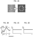
- a power spectrum F(r, ⁇ ) obtained by converting the power spectrum P(k, l) represented by the equation (A) from an orthogonal coordinate system (k, l) to a polar coordinate system (r, ⁇ ) is shown in FIG. 2A where "r" and ⁇ satisfy the equation (C) and the equation (D), respectively.
- variation in power value in the entire range of the ⁇ is preferably 10% or less.
- a state in which the variation in power value is 10% or less means that the first structures are uniformly distributed in an arbitrary direction in the outer surface of the electrophotographic photosensitive drum, that is, the first structure group is isotropically arranged.
- a state in which the first structure group is isotropically arranged is required because the toner can be prevented from escaping at the time of the cleaning, and hence a cleaning property is improved.
- the first structure group may contribute to an improvement in transferability. That is, the first structure group reduces the area of contact between the toner and the outer surface of the photosensitive drum to reduce an adhesive force therebetween, and hence the transferability of an electrostatic image formed on the photosensitive drum can be improved.
- the average particle diameter of the toner is typically from about 6 ⁇ m to about 8 ⁇ m, and hence the appearance period of the first structures is preferably from 1 ⁇ m to 5 ⁇ m, more preferably from 2.5 ⁇ m to 3.5 ⁇ m.
- any shape may be adopted as the shape of the second structures as long as the structures are of such a shape as to be periodically arranged on the outer surface of the photosensitive drum to the extent that the above-mentioned requirements are satisfied.
- a shape having a certain repeating structure such as a network shape, a lattice shape, or a dot, may be adopted, or a random shape like a wrinkle shape may be adopted.
- the periodicity of the appearance of the second structures may be obtained by, as described above, measuring the height information on the second structures arranged on the outer surface of the electrophotographic photosensitive drum and analyzing the result of the measurement through use of two-dimensional Fourier transformation.
- variation in power value in the entire range of the ⁇ is preferably 10% or less.
- a state in which the variation in power value is 10% or less means that the second structures are uniformly distributed in an arbitrary direction in the outer surface of the electrophotographic photosensitive drum, that is, the second structure group is isotropically arranged.
- a state in which the second structure group is isotropically arranged is required because the toner can be prevented from escaping at the time of the cleaning, and hence a cleaning property is improved.
- the second structure group may contribute to a reduction in torque at the time of the cleaning. That is, the second structure group increases the period of the convex shapes on the outer surface of the photosensitive drum to reduce the number of points of contact between the cleaning blade and the outer surface. Thus, the area of contact between the cleaning blade and the outer surface of the photosensitive drum is reduced, and hence the torque at the time of the cleaning can be efficiently reduced. Accordingly, the appearance period of the second structures is preferably from 10 ⁇ m to 50 ⁇ m, more preferably from 20 ⁇ m to 30 ⁇ m.
- the height of the first structure group needs to be lower than the height of the second structure group.
- the height of the first structure group and the height of the second structure group may be the average of the heights of the first structures and the average of the heights of the second structures, respectively.
- the height of the first structure group is lower than the height of the second structure group
- the height of the first structure group and the height of the second structure group are not particularly limited.
- the height of the first structure group is from 0.2 ⁇ m to 2.0 ⁇ m, preferably from 0.5 ⁇ m to 1.0 ⁇ m.
- the height of the second structure group is from 0.5 ⁇ m to 5.0 ⁇ m, preferably from 1.0 ⁇ m to 2.0 ⁇ m.
- the electrophotographic photosensitive drum of the present disclosure is a cylindrical electrophotographic photosensitive member including the support and the photosensitive layer arranged on the support.
- the surface layer of the electrophotographic photosensitive drum contains a curable resin, and the photosensitive layer or a protective layer arranged on the photosensitive layer serves as the surface layer.
- a method of producing the electrophotographic photosensitive drum is, for example, a method involving: preparing coating liquids for the respective layers to be described later; applying the liquids in a desired order of the layers; and drying the liquids.
- examples of the method of applying the coating liquid include dip coating, spray coating, inkjet coating, roll coating, die coating, blade coating, curtain coating, wire bar coating, and ring coating. Of those, dip coating is preferred from the viewpoints of efficiency and productivity.
- the support is preferably a conductive support having conductivity.
- the shape of the support is preferably cylindrical.
- the surface of the support may be subjected to, for example, electrochemical treatment, such as anodization, blast treatment, or cutting treatment.
- a metal, a resin, glass, or the like is preferred as a material for the support.
- Examples of the metal include aluminum, iron, nickel, copper, gold, stainless steel, and alloys thereof. Of those, an aluminum support using aluminum is preferred.
- conductivity may be imparted to the resin or the glass through treatment involving, for example, mixing or coating the resin or the glass with a conductive material.
- metal oxide examples include zinc oxide, aluminum oxide, indium oxide, silicon oxide, zirconium oxide, tin oxide, titanium oxide, magnesium oxide, antimony oxide, and bismuth oxide.
- metal oxide examples include aluminum, nickel, iron, nichrome, copper, zinc, and silver.
- the metal oxide is preferably used as the conductive particles.
- titanium oxide, tin oxide, or zinc oxide is more preferably used.
- the surface of the metal oxide may be treated with a silane coupling agent or the like, or the metal oxide may be doped with an element such as phosphorus or aluminum, or an oxide thereof.
- the conductive particles may each be of a laminated configuration including a core particle and a covering layer covering the core particle.
- a material for the core particle is, for example, titanium oxide, barium sulfate, or zinc oxide.
- a material for the covering layer is, for example, a metal oxide, such as tin oxide.
- the volume-average particle diameter of the particles is preferably from 1 nm to 500 nm, more preferably from 3 nm to 400 nm.
- the resin examples include a polyester resin, a polycarbonate resin, a polyvinyl acetal resin, an acrylic resin, a silicone resin, an epoxy resin, a melamine resin, a polyurethane resin, a phenol resin, and an alkyd resin.
- the conductive layer may further contain, for example, a concealing agent, such as a silicone oil, resin particles, or titanium oxide.
- a concealing agent such as a silicone oil, resin particles, or titanium oxide.
- the average thickness of the conductive layer is preferably from 1 ⁇ m to 50 ⁇ m, particularly preferably from 3 ⁇ m to 40 ⁇ m.
- the conductive layer may be formed by: preparing a coating liquid for a conductive layer containing the above-mentioned respective materials and a solvent; forming a coating film of the coating liquid; and drying the coating film.
- the solvent to be used in the coating liquid include an alcohol-based solvent, a sulfoxide-based solvent, a ketone-based solvent, an ether-based solvent, an ester-based solvent, and an aromatic hydrocarbon-based solvent.
- a dispersion method for the dispersion of the conductive particles in the coating liquid for a conductive layer is, for example, a method including using a paint shaker, a sand mill, a ball mill, or a liquid collision-type highspeed dispersing machine.
- An undercoat layer may be arranged on the support or the conductive layer.
- the arrangement of the undercoat layer can improve an adhesive function between layers to impart a charge injection-inhibiting function.
- the undercoat layer preferably contains a resin.
- the undercoat layer may be formed as a cured film by polymerizing a composition containing a monomer having a polymerizable functional group.
- the resin examples include a polyester resin, a polycarbonate resin, a polyvinyl acetal resin, an acrylic resin, an epoxy resin, a melamine resin, a polyurethane resin, a phenol resin, a polyvinyl phenol resin, an alkyd resin, a polyvinyl alcohol resin, a polyethylene oxide resin, a polypropylene oxide resin, a polyamide resin, a polyamic acid resin, a polyimide resin, a polyamide imide resin, and a cellulose resin.
- a polyester resin examples include a polyester resin, a polycarbonate resin, a polyvinyl acetal resin, an acrylic resin, an epoxy resin, a melamine resin, a polyurethane resin, a phenol resin, a polyvinyl phenol resin, an alkyd resin, a polyvinyl alcohol resin, a polyethylene oxide resin, a polypropylene oxide resin, a polyamide resin, a polyamic acid resin, a polyimide resin
- Examples of the polymerizable functional group of the monomer having the polymerizable functional group include an isocyanate group, a blocked isocyanate group, a methylol group, an alkylated methylol group, an epoxy group, a metal alkoxide group, a hydroxyl group, an amino group, a carboxyl group, a thiol group, a carboxylic acid anhydride group, and a carbon-carbon double bond group.
- the electron-transporting material examples include a quinone compound, an imide compound, a benzimidazole compound, a cyclopentadienylidene compound, a fluorenone compound, a xanthone compound, a benzophenone compound, a cyanovinyl compound, a halogenated aryl compound, a silole compound, and a boron-containing compound.
- An electron-transporting material having a polymerizable functional group may be used as the electron-transporting material and copolymerized with the above-mentioned monomer having a polymerizable functional group to form the undercoat layer as a cured film.
- metal oxide examples include indium tin oxide, tin oxide, indium oxide, titanium oxide, zinc oxide, aluminum oxide, and silicon dioxide.
- metal examples include gold, silver, and aluminum.
- the undercoat layer may further contain an additive.
- the average thickness of the undercoat layer is preferably from 0.1 ⁇ m to 50 ⁇ m, more preferably from 0.2 ⁇ m to 40 ⁇ m, particularly preferably from 0.3 ⁇ m to 30 ⁇ m.
- the undercoat layer may be formed by: preparing a coating liquid for an undercoat layer containing the above-mentioned respective materials and a solvent; forming a coating film of the coating liquid; and drying and/or curing the coating film.
- the solvent to be used in the coating liquid include an alcohol-based solvent, a ketone-based solvent, an ether-based solvent, an ester-based solvent, and an aromatic hydrocarbon-based solvent.
- the photosensitive layer of the electrophotographic photosensitive drum is mainly classified into (1) a laminated photosensitive layer and (2) a single-layer photosensitive layer.
- the laminated photosensitive layer includes a charge-generating layer containing a charge-generating material and a charge-transporting layer containing a charge-transporting material.
- the single-layer photosensitive layer includes a photosensitive layer containing both of the charge-generating material and the charge-transporting material.
- the charge-generating layer and the charge-transporting layer in the laminated photosensitive layer are described below.
- the charge-generating layer preferably contains the charge-generating material and a resin.
- the charge-generating material examples include an azo pigment, a perylene pigment, a polycyclic quinone pigment, an indigo pigment, and a phthalocyanine pigment. Of those, an azo pigment and a phthalocyanine pigment are preferred. Of the phthalocyanine pigments, an oxytitanium phthalocyanine pigment, a chlorogallium phthalocyanine pigment, and a hydroxygallium phthalocyanine pigment are preferred.
- the content of the charge-generating material in the charge-generating layer is preferably from 40 mass% to 85 mass%, more preferably from 60 mass% to 80 mass% with respect to the total mass of the charge-generating layer.
- the resin examples include a polyester resin, a polycarbonate resin, a polyvinyl acetal resin, a polyvinyl butyral resin, an acrylic resin, a silicone resin, an epoxy resin, a melamine resin, a polyurethane resin, a phenol resin, a polyvinyl alcohol resin, a cellulose resin, a polystyrene resin, a polyvinyl acetate resin, and a polyvinyl chloride resin.
- a polyvinyl butyral resin is more preferred.
- the charge-generating layer may further contain an additive, such as an antioxidant or a UV absorber.
- an additive such as an antioxidant or a UV absorber.
- Specific examples thereof include a hindered phenol compound, a hindered amine compound, a sulfur compound, a phosphorus compound, and a benzophenone compound.
- the average thickness of the charge-generating layer is preferably from 0.1 ⁇ m to 1 ⁇ m, more preferably from 0.15 ⁇ m to 0.4 ⁇ m.
- the charge-generating layer may be formed by: preparing a coating liquid for a charge-generating layer containing the above-mentioned respective materials and a solvent; forming a coating film of the coating liquid; and drying the coating film.
- the solvent to be used in the coating liquid include an alcohol-based solvent, a sulfoxide-based solvent, a ketone-based solvent, an ether-based solvent, an ester-based solvent, and an aromatic hydrocarbon-based solvent.
- Examples of the charge-transporting material include a polycyclic aromatic compound, a heterocyclic compound, a hydrazone compound, a styryl compound, an enamine compound, a benzidine compound, a triarylamine compound, and a resin having a group derived from any of those substances.
- a triarylamine compound and a benzidine compound are preferred, and a compound represented by the formula (1) is suitably used.
- R 1 to R 10 each independently represent a hydrogen atom or a methyl group.
- Examples of the compound represented by the formula (1) are represented in the formula (1-1) to the formula (1-10). Of those, the compounds represented by the formula (1-1) to the formula (1-6) are more preferred.
- thermoplastic resin is used as the resin, and examples thereof include a polyester resin, a polycarbonate resin, an acrylic resin, and a polystyrene resin. Of those, a polycarbonate resin and a polyester resin are preferred. As the polyester resin, a polyarylate resin is particularly preferred.
- the content of the charge-transporting material in the charge-transporting layer is preferably from 25 mass% to 70 mass%, more preferably from 30 mass% to 55 mass% with respect to the total mass of the charge-transporting layer.
- a content ratio (mass ratio) between the charge-transporting material and the resin is preferably from 4:10 to 20:10, more preferably from 5:10 to 12:10.
- the charge-transporting layer may contain an additive, such as an antioxidant, a UV absorber, a plasticizer, a leveling agent, a lubricity-imparting agent, or an abrasion resistance-improving agent.
- an additive such as an antioxidant, a UV absorber, a plasticizer, a leveling agent, a lubricity-imparting agent, or an abrasion resistance-improving agent.
- Specific examples thereof include a hindered phenol compound, a hindered amine compound, a sulfur compound, a phosphorus compound, a benzophenone compound, a siloxane-modified resin, a silicone oil, fluorine resin particles, polystyrene resin particles, polyethylene resin particles, silica particles, alumina particles, and boron nitride particles.
- the average thickness of the charge-transporting layer is preferably from 5 ⁇ m to 50 ⁇ m, more preferably from 8 ⁇ m to 40 ⁇ m, particularly preferably from 10 ⁇ m to 30 ⁇ m.
- the charge-transporting layer may be formed by: preparing a coating liquid for a charge-transporting layer containing the above-mentioned respective materials and a solvent; forming a coating film of the coating liquid; and drying the coating film.
- the solvent to be used in the coating liquid include an alcohol-based solvent, a ketone-based solvent, an ether-based solvent, an ester-based solvent, and an aromatic hydrocarbon-based solvent. Of those solvents, an ether-based solvent or an aromatic hydrocarbon-based solvent is preferred.
- the single-layer photosensitive layer may be formed by: preparing a coating liquid for a photosensitive layer containing the charge-generating material, the charge-transporting material, a resin, and a solvent; forming a coating film of the coating liquid; and drying the coating film.
- the charge-generating material, the charge-transporting material, and the resin are the same as the examples of the materials in the above-mentioned section "(1) Laminated Photosensitive Layer".
- a protective layer may be arranged on the photosensitive layer.
- the arrangement of the protective layer can improve the durability of the photosensitive drum.
- Examples of the conductive particles include metal oxide particles, such as titanium oxide, zinc oxide, tin oxide, and indium oxide.
- Examples of the compound having one polymerizable functional group are represented in the formula (2-1) to the formula (2-6).
- Examples of the compound having a plurality of polymerizable functional groups are represented in the formula (3-1) to the formula (3-7).
- the method of forming the wrinkle shapes includes: forming the protective layer that is a crosslinkable cured film on the charge-transporting layer containing the thermoplastic resin as a main component in the case of the laminated photosensitive layer, or on the single-layer photosensitive layer containing the thermoplastic resin as a main component in the case of the single-layer photosensitive layer; and then subjecting the laminate to heating treatment to produce the wrinkle shapes. Accordingly, when the wrinkle shapes are formed by the method, the outer surface of the electrophotographic photosensitive drum is always the surface of the protective layer arranged directly above the photosensitive layer.
- all the reference lines intersect the wrinkle shapes at a plurality of sites at different intersection angles, and hence the ridge lines of the wrinkle shapes each have a plurality of curvatures therein.
- FIG. 5A , FIG. 6A , and FIG. 7A are views obtained by viewing the surface of the electrophotographic photosensitive drum from above.
- FIG. 5B , FIG. 6B , and FIG. 7A are views obtained by viewing the surface of the electrophotographic photosensitive drum from above.
- the charge-transporting layer or the single-layer photosensitive layer is formed through the first heating treatment including gradually heating the coating film of the coating liquid at a heating temperature lower than the boiling point of the first solvent to dry the coating film.
- the first heating treatment suppresses rapid evaporation of the solvents from the charge-transporting layer or the single-layer photosensitive layer and rapid curing of the photosensitive layer, and hence the first solvent and the second solvent having different boiling points are each present while being uniformly distributed in the charge-transporting layer or the single-layer photosensitive layer after the first heating treatment.
- the amount of the first solvent when the amount of the second solvent in the charge-transporting layer or the single-layer photosensitive layer after the first heating treatment is less than 0.50 mass%, the fine wrinkle shapes are hardly formed, and when the amount is more than 2.50 mass%, the degree of the buckling may become larger to enlarge the wrinkle shapes or to reduce the uniformity of the wrinkle shapes.
- the coating film be gradually heated from room temperature to a temperature lower than the boiling point of the first solvent by about 10°C over about 1 hour.
- the coating film is preferably heated at a heating temperature higher than the boiling point of the second solvent by about 30°C for a time period that is from about 1.5 times to about 2.5 times as long as the time period of the first heating treatment.
- the method of forming the structures through embossing is, for example, a method including bringing a mold member having an uneven shape into pressure contact with the electrophotographic photosensitive drum to transfer the uneven shape of the mold member onto the surface of the electrophotographic photosensitive drum.
- the structure groups may be formed through embossing also in a photosensitive drum having a protective layer.
- the heights of the first structures and the second structures are each a difference in height between the apex of the structure and the bottom point of the concave shape thereof.
- the average of the heights of the first structures and the average of the heights of the second structures may be determined from the entire region of the photosensitive drum, or may be determined from height information measured in an arbitrary square region 500 ⁇ m on a side.
- FIG. 8 is an illustration of an example of a pressure-contact shape transfer processing apparatus for forming concave portions on the surface of the electrophotographic photosensitive drum.
- the concave portions can be formed on the surface of an electrophotographic photosensitive drum 2-1 serving as a work piece by continuously bringing a mold member 2-2 into contact with the outer surface of the electrophotographic photosensitive drum 2-1 to pressurize the outer surface while rotating the photosensitive drum.
- the example illustrated in FIG. 8 is an example in which the pressurizing member 2-3 is moved in a direction vertical to the shaft direction of the electrophotographic photosensitive drum 2-1 to continuously process the surface of the electrophotographic photosensitive drum 2-1 while causing or driving the photosensitive drum to rotate. Further, the surface of the electrophotographic photosensitive drum 2-1 may be continuously processed by moving the supporting members 2-4 in the direction vertical to the shaft direction of the electrophotographic photosensitive drum 2-1 while fixing the pressurizing member 2-3, or by moving both of the supporting members 2-4 and the pressurizing member 2-3.
- the mold member 2-2 and the electrophotographic photosensitive drum 2-1 are preferably heated from the viewpoint of efficiently transferring the shape of the mold member.
- Examples of the mold member 2-2 include: a metal or a resin film subjected to fine surface processing; a product obtained by pattering the surface of a silicon wafer or the like with a resist; a resin film having dispersed therein fine particles; and a product obtained by coating a resin film having a fine surface shape with a metal.
- the mold member 2-2 is preferably heated so that the temperature of the surface of the electrophotographic photosensitive drum 2-1 in the portion of the photosensitive drum brought into pressure contact with the mold member 2-2 may be equal to or more than the glass transition point Tg of the resin in the surface layer of the photosensitive drum.
- the following microscopes may each be utilized as the atomic force microscope.
- the following microscopes may each be utilized as the electron microscope.
- the height information on the resultant electrophotographic photosensitive drum can be obtained by measuring the height information on the outer surface thereof obtained from the three-dimensional surface shape data and analyzing the result through use of two-dimensional Fourier transformation.
- the radial direction distribution function p(r) obtained by turning the power spectrum F(r, ⁇ ) of the uneven shape of the outer surface into a one-dimension in the radial direction is subjected to frequency analysis, followed by the determination of the angle distribution q1( ⁇ 1 ) of a two-dimensional power spectrum F 1 (rp 1 , ⁇ 1 ) at the frequency rp1 at which the radial direction distribution function p(r) becomes a local maximum, and the angle distribution q2( ⁇ 2 ) of a two-dimensional power spectrum F 2 (rp 2 , ⁇ 2 ) at the frequency rp2 at which the radial direction distribution function p(r) becomes a local maximum.
- An approach to evaluating the distribution function of the uneven shape of the resultant electrophotographic photosensitive drum includes judging whether or not the radial direction distribution function p(r) has a plurality of peaks. That is, when the radial direction distribution function p(r) of the uneven shape has at least two peaks, and the average of the heights of the structures of the photosensitive drum corresponding to a peak at higher frequencies is lower than the average of the heights of the structures thereof corresponding to a peak at lower frequencies, the requirements of the electrophotographic photosensitive drum of the present disclosure are satisfied. Further, the approach includes judging whether or not the angle distributions q1( ⁇ ) and q2( ⁇ ) are each uniform in the entire range of the ⁇ .
- a case in which variation in power value F 1 in the entire range of the ⁇ 1 is 10% or less, and variation in power value F 2 in the entire range of the ⁇ 2 is 10% or less means that the first structures and the second structures are isotropically arranged on the outer surface of the electrophotographic photosensitive drum.
- the features of the surface shape of the electrophotographic photosensitive drum can be judged through the foregoing processing.
- a process cartridge of the present disclosure integrally supports the electrophotographic photosensitive drum described above, and at least one unit selected from the group consisting of a charging unit, a developing unit, a transferring unit, and a cleaning unit, and is removably mounted onto a main body of an electrophotographic image forming apparatus.
- an electrophotographic image forming apparatus of the present disclosure includes the electrophotographic photosensitive drum described above, and at least one unit selected from the group consisting of a charging unit, an exposing unit, a developing unit, and a transferring unit.
- FIG. 9 An example of the schematic construction of an electrophotographic image forming apparatus including a process cartridge including an electrophotographic photosensitive drum is illustrated in FIG. 9 .
- a cylindrical electrophotographic photosensitive drum 1 is rotationally driven about a shaft 2 in an arrow direction at a predetermined peripheral speed.
- the surface of the electrophotographic photosensitive drum 1 is charged to a predetermined positive or negative potential by a charging unit 3.
- a roller charging system based on a roller type charging member is illustrated in FIG. 9 , a charging system such as a corona charging system, a proximity charging system, or an injection charging system may be adopted.
- the charged surface of the electrophotographic photosensitive drum 1 is irradiated with exposure light 4 from an exposing unit (not shown), and hence an electrostatic latent image corresponding to target image information is formed thereon.
- the electrostatic latent image formed on the surface of the electrophotographic photosensitive drum 1 is developed with a toner stored in a developing unit 5, and a toner image is formed on the surface of the electrophotographic photosensitive drum 1.
- the toner image formed on the surface of the electrophotographic photosensitive drum 1 is transferred onto a transfer material 7 by a transferring unit 6.
- the transfer material 7 onto which the toner image has been transferred is conveyed to a fixing unit 8, is subjected to treatment for fixing the toner image, and is printed out to the outside of the electrophotographic image forming apparatus.
- the electrophotographic image forming apparatus may include a cleaning unit 9 for removing a deposit, such as the toner remaining on the surface of the electrophotographic photosensitive drum 1 after the transfer.
- the electrophotographic image forming apparatus may include an electricity-removing mechanism configured to subject the surface of the electrophotographic photosensitive drum 1 to electricity-removing treatment with pre-exposure light 10 from a pre-exposing unit (not shown).
- a guiding unit 12, such as a rail, may be arranged for removably mounting a process cartridge 11 onto the main body of an electrophotographic image forming apparatus.
- the electrophotographic photosensitive drum may be used in, for example, a laser beam printer, an LED printer, and a copying machine.
- both of a reduction in torque of the electrophotographic photosensitive drum at the time of its cleaning and an improvement in image transferability can be achieved.
- An aluminum cylinder (JIS-A3003, aluminum alloy) having a diameter of 24 mm and a length of 257.5 mm was used as a support (conductive support).
- the addition amount of the silicone resin particles was set to 10 mass% with respect to the total mass of the metal oxide particles and the binding material in the dispersion liquid after the removal of the glass beads.
- a silicone oil product name: SH28PA, manufactured by Dow Corning Toray Co., Ltd.
- SH28PA manufactured by Dow Corning Toray Co., Ltd.
- a mixed solvent of methanol and 1-methoxy-2-propanol (mass ratio: 1:1) was added to the dispersion liquid so that the total mass of the metal oxide particles, the binding material, and the surface roughness-imparting agent (i.e., the mass of a solid content) in the dispersion liquid became 67 mass% with respect to the mass of the dispersion liquid.
- the mixture was stirred to prepare a coating liquid for a conductive layer.
- the coating liquid for a conductive layer was applied onto the support by dip coating, and the applied liquid was heated at 140°C for 1 hour to form a conductive layer having a thickness of 30 ⁇ m.
- Electrode-transporting material represented by the formula (E-1) 4 parts ⁇ Blocked isocyanate (product name: DURANATE SBN-70D, manufactured by Asahi Kasei Chemicals Corporation) 5.5 parts ⁇ Polyvinyl butyral resin (S-LEC KS-5Z, manufactured by Sekisui Chemical Co., Ltd.) 0.3 part ⁇ Zinc(II) hexanoate serving as a catalyst (manufactured by Mitsuwa Chemicals Co., Ltd.) 0.05 part
- Those materials were dissolved in a mixed solvent of 60 parts of toluene, 2.3 parts of methyl benzoate, and 12.8 parts of tetrahydrofuran to prepare a coating liquid for a charge-transporting layer.
- the coating liquid for a charge-transporting layer was applied onto the charge-generating layer by dip coating to form a coating film, and the coating film was dried at 100°C for 20 minutes to form a charge-transporting layer having a thickness of 16 ⁇ m.
- the remaining solvent amounts of the charge-transporting layer were measured with a gas chromatography mass spectrometer (product name: HP6890, manufactured by Hewlett-Packard Company) including a head space sampler and a detector (product name: HP5973, manufactured by Hewlett-Packard Company).
- a gas chromatography mass spectrometer product name: HP6890, manufactured by Hewlett-Packard Company
- HP5973 manufactured by Hewlett-Packard Company
- the measurement was performed by using HP-5MS (copolymer containing 5% of diphenylpolysiloxane and 95% of dimethylpolysiloxane, thickness: 0.25 ⁇ m, inner diameter: 0.25 mm, length: 30 m) manufactured by Hewlett-Packard Company as a capillary column and He (1 ml/min) as a carrier gas under the following conditions: the column was held at 40°C for 3 minutes; as a first-stage temperature increase, the temperature of the column was increased from 40°C to 70°C at a rate of temperature increase of 2°C/min; as a second-stage temperature increase, the temperature of the column was increased from 70°C to 150°C at a rate of temperature increase of 5°C/min; and as a third-stage temperature increase, the temperature of the column was increased from 150°C to 300°C at a rate of temperature increase of 10°C/min.
- a calibration curve was produced by using the solvents to be used in the charge-transporting layer as reference substances
- An electrophotographic photosensitive drum was produced in the same manner as in Example 1 except that: the kinds of the charge-transporting materials were changed as shown in Table 1; and the conditions under which the second heating treatment was performed were changed as shown in Table 2.
- a photosensitive drum produced as follows was prepared: the temperature of the second heating treatment of the electrophotographic photosensitive drum of Example 1 was changed to 120°C, and no wrinkle shapes were formed.
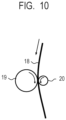
- the outer surface of the photosensitive drum was polished with a polishing machine illustrated in FIG. 10 under the following conditions. Feeding speed of a polishing sheet: 400 mm/min Number of revolutions of the photosensitive drum: 240 rpm Polishing grains: Silicon carbide Average particle diameter of the polishing grains: 3 ⁇ m Polishing time: 20 seconds
- a method for the polishing was as described below. While a polishing sheet 18 obtained by arranging, on a sheet-shaped substrate, a layer obtained by dispersing the polishing grains in a binder resin was fed in an arrow direction, an electrophotographic photosensitive drum 19 was subjected to surface roughening treatment by being pressed against a backup roller 20 for 20 seconds while being rotated in an arrow direction. Thus, an electrophotographic photosensitive drum having a flaw in its peripheral direction was produced. The surface roughness Ra of the photosensitive drum after the surface roughening was evaluated under the same conditions as those of the measurement of an appearance period. As a result, the surface roughness was 0.018 ⁇ m.
- each of the electrophotographic photosensitive drums of Examples 1 to 5 was observed with a laser microscope (product name: VK-X200, manufactured by Keyence Corporation) at a certain magnification, and the number of the peaks of structures included in each of a first structure group and a second structure group, and the appearance period, average height, and isotropy of the structures were evaluated through the analysis of the resultant data by the methods described above.
- the appearance period was calculated from the frequency of the peaks.
- the angle distribution q( ⁇ ) of a power spectrum F(rp, ⁇ ) was calculated at the frequency at which the appearance of each of the first structure group and the second structure group became a local maximum, and when variation in power value in the entire range of the ⁇ was 10% or less, the structures were judged to be isotropic.
- Visual observation of the peripheral surface shape of the electrophotographic photosensitive drum of Comparative Example 1 showed that shapes on its surface were anisotropically arranged. The results are shown in Table 3.
- the photosensitive drums of Examples and Comparative Example were each mounted on the cyan color cartridge of the image forming apparatus, and a test chart having a print percentage of 5% was output on 100 sheets of A4 size plain paper.
- a charging condition a dark portion potential was adjusted to -500 V, and as an exposure condition, the image exposure light quantity was adjusted to 0.25 ⁇ J/cm 2 .
- a drive current value at the time of the output on the 100th sheet with the evaluation apparatus was defined as a current value A.
- an electrophotographic photosensitive drum free of any wrinkle shapes on its outer surface was produced in the same manner as in the production of the electrophotographic photosensitive drum of Example 1 except that the second heating treatment was not performed.
- the drum was defined as a control electrophotographic photosensitive drum.
- the control electrophotographic photosensitive drum was mounted on the evaluation apparatus, and a drive current value at the time of the output of the test chart on the 100th sheet of the plain paper with the apparatus was defined as a current value B.
- the ratio (current value A/current value B) of the current value A to the current value B thus obtained was defined as a torque relative value.
- a case in which the torque relative value is 0.7 or less means that a frictional force between the electrophotographic photosensitive drum and a cleaning blade is sufficiently reduced.
- the electrophotographic photosensitive drum includes: a support; and a photosensitive layer arranged on the support, the electrophotographic photosensitive drum having arranged on an outer surface thereof at least two structure groups having different appearance periods, wherein when, out of the two structure groups, a group including structures having a smaller appearance period is defined as a first structure group, and a group including structures having a larger appearance period is defined as a second structure group, a height of the first structure group is lower than a height of the second structure group.
Landscapes
- Physics & Mathematics (AREA)
- General Physics & Mathematics (AREA)
- Spectroscopy & Molecular Physics (AREA)
- Photoreceptors In Electrophotography (AREA)
Applications Claiming Priority (1)
| Application Number | Priority Date | Filing Date | Title |
|---|---|---|---|
| JP2020075648A JP7483477B2 (ja) | 2020-04-21 | 2020-04-21 | 電子写真感光ドラム、プロセスカートリッジおよび電子写真画像形成装置 |
Publications (2)
| Publication Number | Publication Date |
|---|---|
| EP3901702A1 EP3901702A1 (en) | 2021-10-27 |
| EP3901702B1 true EP3901702B1 (en) | 2025-06-25 |
Family
ID=75581430
Family Applications (1)
| Application Number | Title | Priority Date | Filing Date |
|---|---|---|---|
| EP21169075.5A Active EP3901702B1 (en) | 2020-04-21 | 2021-04-19 | Electrophotographic photosensitive member, process cartridge, and electrophotographic image forming apparatus |
Country Status (3)
| Country | Link |
|---|---|
| US (1) | US11392074B2 (enExample) |
| EP (1) | EP3901702B1 (enExample) |
| JP (1) | JP7483477B2 (enExample) |
Families Citing this family (8)
| Publication number | Priority date | Publication date | Assignee | Title |
|---|---|---|---|---|
| US11619907B2 (en) * | 2021-03-10 | 2023-04-04 | Canon Kabushiki Kaisha | Process cartridge |
| DE112022003014T5 (de) | 2021-06-11 | 2024-04-25 | Canon Kabushiki Kaisha | Elektrophotographisches lichtempfindliches element, prozesskartusche und elektrophotographisches gerät |
| WO2022260036A1 (ja) | 2021-06-11 | 2022-12-15 | キヤノン株式会社 | 電子写真感光体、プロセスカートリッジ及び電子写真装置 |
| JP7691305B2 (ja) | 2021-08-06 | 2025-06-11 | キヤノン株式会社 | 電子写真感光体、プロセスカートリッジ及び電子写真装置 |
| JP7752992B2 (ja) | 2021-08-06 | 2025-10-14 | キヤノン株式会社 | 電子写真装置 |
| JP7752991B2 (ja) | 2021-08-06 | 2025-10-14 | キヤノン株式会社 | 電子写真装置 |
| JP2023061679A (ja) | 2021-10-20 | 2023-05-02 | キヤノン株式会社 | 電子写真感光体、プロセスカートリッジ、および電子写真装置 |
| JP2023131675A (ja) | 2022-03-09 | 2023-09-22 | キヤノン株式会社 | 電子写真装置 |
Family Cites Families (83)
| Publication number | Priority date | Publication date | Assignee | Title |
|---|---|---|---|---|
| JPH0727267B2 (ja) * | 1986-10-04 | 1995-03-29 | ミノルタ株式会社 | 電子写真の感光体 |
| US4908330A (en) | 1988-02-01 | 1990-03-13 | Canon Kabushiki Kaisha | Process for the formation of a functional deposited film containing group IV atoms or silicon atoms and group IV atoms by microwave plasma chemical vapor deposition process |
| JPH01198481A (ja) | 1988-02-01 | 1989-08-10 | Canon Inc | マイクロ波プラズマcvd法による堆積膜形成法 |
| JP2992638B2 (ja) | 1995-06-28 | 1999-12-20 | キヤノン株式会社 | 光起電力素子の電極構造及び製造方法並びに太陽電池 |
| CN1306342C (zh) | 2002-04-26 | 2007-03-21 | 佳能株式会社 | 电摄影感光体、成像处理盒和电摄影装置 |
| JP4174391B2 (ja) | 2002-08-30 | 2008-10-29 | キヤノン株式会社 | 電子写真感光体、プロセスカートリッジおよび電子写真装置 |
| US7001699B2 (en) | 2002-08-30 | 2006-02-21 | Canon Kabushiki Kaisha | Electrophotographic photosensitive member, process cartridge and electrophotographic apparatus |
| US7266329B2 (en) | 2003-09-29 | 2007-09-04 | Canon Kabushiki Kaisha | Toner image carrying member and manufacturing method thereof, and electrophotographic apparatus |
| JP4169726B2 (ja) | 2004-06-25 | 2008-10-22 | 株式会社リコー | 電子写真感光体、画像形成装置、及びプロセスカートリッジ |
| KR101017442B1 (ko) | 2005-12-07 | 2011-02-25 | 캐논 가부시끼가이샤 | 폴리비닐아세탈 수지, 전자 사진 감광체, 공정 카트리지 및전자 사진 장치 |
| KR101243483B1 (ko) | 2007-12-04 | 2013-03-13 | 캐논 가부시끼가이샤 | 전자 사진 감광체, 전자 사진 감광체의 제조 방법, 프로세스 카트리지 및 전자 사진 장치 |
| JP2010026240A (ja) | 2008-07-18 | 2010-02-04 | Canon Inc | 電子写真感光体、プロセスカートリッジ及び電子写真装置 |
| JP2010066670A (ja) * | 2008-09-12 | 2010-03-25 | Canon Inc | 電子写真感光体の製造方法 |
| JP5549917B2 (ja) * | 2008-11-07 | 2014-07-16 | 株式会社リコー | 電子写真感光体、それを用いた画像形成方法、画像形成装置及び画像形成装置用プロセスカートリッジ |
| JP4696174B2 (ja) | 2009-04-23 | 2011-06-08 | キヤノン株式会社 | 電子写真感光体の製造方法 |
| JP5081271B2 (ja) | 2009-04-23 | 2012-11-28 | キヤノン株式会社 | 電子写真感光体、プロセスカートリッジおよび電子写真装置 |
| JP4743921B1 (ja) | 2009-09-04 | 2011-08-10 | キヤノン株式会社 | 電子写真感光体、プロセスカートリッジおよび電子写真装置 |
| JP5054238B1 (ja) | 2011-03-03 | 2012-10-24 | キヤノン株式会社 | 電子写真感光体の製造方法 |
| JP5755162B2 (ja) | 2011-03-03 | 2015-07-29 | キヤノン株式会社 | 電子写真感光体の製造方法 |
| JP5079153B1 (ja) | 2011-03-03 | 2012-11-21 | キヤノン株式会社 | 電子写真感光体、プロセスカートリッジおよび電子写真装置、ならびに、電子写真感光体の製造方法 |
| JP6039368B2 (ja) | 2011-11-30 | 2016-12-07 | キヤノン株式会社 | 電子写真感光体、プロセスカートリッジおよび電子写真装置、ならびに、ガリウムフタロシアニン結晶 |
| JP6071439B2 (ja) | 2011-11-30 | 2017-02-01 | キヤノン株式会社 | フタロシアニン結晶の製造方法、および電子写真感光体の製造方法 |
| JP5993720B2 (ja) | 2011-11-30 | 2016-09-14 | キヤノン株式会社 | 電子写真感光体、プロセスカートリッジおよび電子写真装置 |
| JP5827612B2 (ja) | 2011-11-30 | 2015-12-02 | キヤノン株式会社 | ガリウムフタロシアニン結晶の製造方法、及び該ガリウムフタロシアニン結晶の製造方法を用いた電子写真感光体の製造方法 |
| JP6105974B2 (ja) | 2012-03-15 | 2017-03-29 | キヤノン株式会社 | 電子写真感光体の製造方法、および電荷輸送層用乳化液 |
| JP6105973B2 (ja) | 2012-03-22 | 2017-03-29 | キヤノン株式会社 | 電子写真感光体の製造方法、電荷輸送層用乳化液 |
| JP6049329B2 (ja) | 2012-06-29 | 2016-12-21 | キヤノン株式会社 | 電子写真感光体、電子写真感光体の製造方法、プロセスカートリッジおよび電子写真装置 |
| US9029054B2 (en) | 2012-06-29 | 2015-05-12 | Canon Kabushiki Kaisha | Electrophotographic photosensitive member, process cartridge, and electrophotographic apparatus |
| EP2680075B1 (en) | 2012-06-29 | 2015-12-30 | Canon Kabushiki Kaisha | Electrophotographic photosensitive member, process cartridge, and electrophotographic apparatus |
| JP6108842B2 (ja) | 2012-06-29 | 2017-04-05 | キヤノン株式会社 | 電子写真感光体の製造方法 |
| US9063505B2 (en) | 2012-06-29 | 2015-06-23 | Canon Kabushiki Kaisha | Electrophotographic photosensitive member, process cartridge, and electrophotographic apparatus |
| JP6218502B2 (ja) | 2012-08-30 | 2017-10-25 | キヤノン株式会社 | 電子写真感光体、プロセスカートリッジおよび電子写真装置 |
| JP6061761B2 (ja) | 2012-08-30 | 2017-01-18 | キヤノン株式会社 | 電子写真感光体、プロセスカートリッジおよび電子写真装置 |
| JP6423697B2 (ja) | 2013-12-26 | 2018-11-14 | キヤノン株式会社 | 電子写真感光体、電子写真感光体の製造方法、プロセスカートリッジおよび電子写真装置 |
| JP6555877B2 (ja) | 2013-12-26 | 2019-08-07 | キヤノン株式会社 | 電子写真感光体、及び、該電子写真感光体の製造方法、及び該電子写真感光体を有するプロセスカートリッジ及び電子写真装置 |
| JP2015143831A (ja) | 2013-12-26 | 2015-08-06 | キヤノン株式会社 | 電子写真感光体、プロセスカートリッジ及び電子写真装置 |
| JP6456126B2 (ja) | 2013-12-26 | 2019-01-23 | キヤノン株式会社 | 電子写真感光体の製造方法 |
| JP6463104B2 (ja) | 2013-12-26 | 2019-01-30 | キヤノン株式会社 | 電子写真感光体、プロセスカートリッジ及び電子写真装置 |
| JP2015143822A (ja) | 2013-12-26 | 2015-08-06 | キヤノン株式会社 | 電子写真感光体、プロセスカートリッジ及び電子写真装置 |
| JP6403586B2 (ja) * | 2014-02-21 | 2018-10-10 | キヤノン株式会社 | 電子写真感光体、プロセスカートリッジおよび電子写真装置 |
| JP6429636B2 (ja) | 2014-02-24 | 2018-11-28 | キヤノン株式会社 | 電子写真感光体、プロセスカートリッジおよび電子写真装置 |
| JP6317597B2 (ja) | 2014-02-27 | 2018-04-25 | キヤノン株式会社 | 電子写真感光体の表面加工方法、および表面に凹凸形状を有する電子写真感光体の製造方法 |
| JP6444085B2 (ja) | 2014-07-23 | 2018-12-26 | キヤノン株式会社 | 電子写真感光体の製造方法 |
| US9684277B2 (en) | 2014-11-19 | 2017-06-20 | Canon Kabushiki Kaisha | Process cartridge and image-forming method |
| US9599917B2 (en) | 2014-12-26 | 2017-03-21 | Canon Kabushiki Kaisha | Electrophotographic photosensitive member, process cartridge and electrophotographic apparatus |
| JP6508948B2 (ja) | 2015-01-26 | 2019-05-08 | キヤノン株式会社 | 電子写真感光体、電子写真感光体の製造方法、プロセスカートリッジおよび電子写真装置 |
| JP2017010009A (ja) | 2015-06-24 | 2017-01-12 | キヤノン株式会社 | 電子写真感光体、プロセスカートリッジおよび電子写真装置 |
| US20170060008A1 (en) | 2015-08-27 | 2017-03-02 | Canon Kabushiki Kaisha | Image forming method, process cartridge and electrophotographic apparatus |
| JP6639256B2 (ja) | 2016-02-10 | 2020-02-05 | キヤノン株式会社 | 電子写真装置、およびプロセスカートリッジ |
| JP6723790B2 (ja) | 2016-03-31 | 2020-07-15 | キヤノン株式会社 | 電子写真感光体、プロセスカートリッジおよび電子写真装置 |
| US10095137B2 (en) | 2016-04-04 | 2018-10-09 | Canon Kabushiki Kaisha | Electrophotographic photosensitive member, method of producing electrophotographic photosensitive member, process cartridge, and electrophotographic image forming apparatus |
| JP6978858B2 (ja) | 2016-06-21 | 2021-12-08 | キヤノン株式会社 | 電子写真感光体、電子写真感光体の製造方法、該電子写真感光体を有するプロセスカートリッジおよび電子写真装置 |
| US10416581B2 (en) | 2016-08-26 | 2019-09-17 | Canon Kabushiki Kaisha | Electrophotographic photosensitive member, process cartridge, and electrophotographic apparatus |
| JP6824731B2 (ja) * | 2016-12-28 | 2021-02-03 | キヤノン株式会社 | 電子写真感光体、プロセスカートリッジ及び電子写真装置 |
| JP6921612B2 (ja) * | 2017-05-02 | 2021-08-18 | キヤノン株式会社 | 画像形成装置 |
| JP7060923B2 (ja) | 2017-05-25 | 2022-04-27 | キヤノン株式会社 | 電子写真感光体、プロセスカートリッジおよび電子写真装置 |
| JP6921651B2 (ja) * | 2017-06-29 | 2021-08-18 | キヤノン株式会社 | 電子写真感光体、プロセスカートリッジ及び電子写真装置 |
| JP7187270B2 (ja) | 2017-11-24 | 2022-12-12 | キヤノン株式会社 | プロセスカートリッジ及び電子写真装置 |
| JP7046571B2 (ja) * | 2017-11-24 | 2022-04-04 | キヤノン株式会社 | プロセスカートリッジ及び電子写真装置 |
| JP7057104B2 (ja) | 2017-11-24 | 2022-04-19 | キヤノン株式会社 | プロセスカートリッジ及び電子写真画像形成装置 |
| JP7034769B2 (ja) | 2018-02-28 | 2022-03-14 | キヤノン株式会社 | 電子写真感光体、プロセスカートリッジ及び電子写真装置 |
| JP2019152699A (ja) | 2018-02-28 | 2019-09-12 | キヤノン株式会社 | 電子写真感光体、プロセスカートリッジ及び電子写真装置 |
| JP7034768B2 (ja) | 2018-02-28 | 2022-03-14 | キヤノン株式会社 | プロセスカートリッジ及び画像形成装置 |
| US10747130B2 (en) | 2018-05-31 | 2020-08-18 | Canon Kabushiki Kaisha | Process cartridge and electrophotographic apparatus |
| JP7059112B2 (ja) | 2018-05-31 | 2022-04-25 | キヤノン株式会社 | 電子写真感光体、プロセスカートリッジおよび電子写真画像形成装置 |
| JP7059111B2 (ja) | 2018-05-31 | 2022-04-25 | キヤノン株式会社 | 電子写真感光体およびその製造方法、並びにプロセスカートリッジおよび電子写真画像形成装置 |
| JP7054366B2 (ja) | 2018-05-31 | 2022-04-13 | キヤノン株式会社 | 電子写真感光体、プロセスカートリッジおよび電子写真装置 |
| JP7150485B2 (ja) | 2018-05-31 | 2022-10-11 | キヤノン株式会社 | 電子写真感光体、プロセスカートリッジ及び電子写真装置 |
| JP7129225B2 (ja) | 2018-05-31 | 2022-09-01 | キヤノン株式会社 | 電子写真感光体および電子写真感光体の製造方法 |
| JP7222670B2 (ja) * | 2018-11-16 | 2023-02-15 | キヤノン株式会社 | 電子写真感光体の製造方法 |
| JP2020085991A (ja) | 2018-11-19 | 2020-06-04 | キヤノン株式会社 | 電子写真感光体、プロセスカートリッジ及び電子写真装置 |
| JP2020086308A (ja) | 2018-11-29 | 2020-06-04 | キヤノン株式会社 | 電子写真感光体、電子写真装置、およびプロセスカートリッジ |
| JP7413054B2 (ja) | 2019-02-14 | 2024-01-15 | キヤノン株式会社 | 電子写真感光体、プロセスカートリッジおよび電子写真装置 |
| JP7358276B2 (ja) | 2019-03-15 | 2023-10-10 | キヤノン株式会社 | 電子写真画像形成装置及びプロセスカートリッジ |
| JP7301613B2 (ja) | 2019-06-14 | 2023-07-03 | キヤノン株式会社 | 電子写真感光体、プロセスカートリッジ及び電子写真装置 |
| JP7353824B2 (ja) | 2019-06-25 | 2023-10-02 | キヤノン株式会社 | 電子写真感光体、プロセスカートリッジおよび電子写真装置 |
| JP7269111B2 (ja) | 2019-06-25 | 2023-05-08 | キヤノン株式会社 | 電子写真感光体、プロセスカートリッジおよび電子写真装置 |
| JP7305458B2 (ja) | 2019-06-25 | 2023-07-10 | キヤノン株式会社 | 電子写真感光体、プロセスカートリッジ及び電子写真装置 |
| US11126097B2 (en) | 2019-06-25 | 2021-09-21 | Canon Kabushiki Kaisha | Electrophotographic photosensitive member, process cartridge, and electrophotographic apparatus |
| US11573499B2 (en) | 2019-07-25 | 2023-02-07 | Canon Kabushiki Kaisha | Process cartridge and electrophotographic apparatus |
| US11320754B2 (en) | 2019-07-25 | 2022-05-03 | Canon Kabushiki Kaisha | Process cartridge and electrophotographic apparatus |
| JP7337652B2 (ja) | 2019-10-18 | 2023-09-04 | キヤノン株式会社 | プロセスカートリッジ及びそれを用いた電子写真装置 |
| JP7337649B2 (ja) | 2019-10-18 | 2023-09-04 | キヤノン株式会社 | プロセスカートリッジ及び電子写真装置 |
-
2020
- 2020-04-21 JP JP2020075648A patent/JP7483477B2/ja active Active
-
2021
- 2021-04-13 US US17/228,879 patent/US11392074B2/en active Active
- 2021-04-19 EP EP21169075.5A patent/EP3901702B1/en active Active
Also Published As
| Publication number | Publication date |
|---|---|
| JP2021173806A (ja) | 2021-11-01 |
| US20210325814A1 (en) | 2021-10-21 |
| US11392074B2 (en) | 2022-07-19 |
| JP7483477B2 (ja) | 2024-05-15 |
| EP3901702A1 (en) | 2021-10-27 |
Similar Documents
| Publication | Publication Date | Title |
|---|---|---|
| EP3901702B1 (en) | Electrophotographic photosensitive member, process cartridge, and electrophotographic image forming apparatus | |
| US10838315B2 (en) | Electrophotographic photosensitive member, process cartridge and electrophotographic apparatus | |
| EP3367169B1 (en) | Electrophotographic photosensitive member, process cartridge and electrophotographic apparatus | |
| EP3901703B1 (en) | Electrophotographic photosensitive member | |
| US11256186B2 (en) | Electrophotographic photosensitive member, process cartridge and electrophotographic apparatus | |
| US10691033B2 (en) | Electrophotographic photosensitive member, process cartridge, and electrophotographic apparatus | |
| EP3534214B1 (en) | Process cartridge and image-forming apparatus | |
| US10747131B2 (en) | Electrophotographic photosensitive member and method for manufacturing the same as well as process cartridge and electrophotographic image-forming apparatus | |
| US10203617B2 (en) | Electrophotographic photosensitive member, process cartridge and electrophotographic apparatus | |
| US9389521B2 (en) | Electrophotographic photosensitive member, process cartridge, and electrophotographic apparatus | |
| US11782353B2 (en) | Method for producing electrophotographic photosensitive member | |
| EP3525042B1 (en) | Electrophotographic photosensitive member, process cartridge, and electrophotographic apparatus | |
| EP4170431A1 (en) | Electrophotographic photosensitive member, process cartridge, and electrophotographic apparatus | |
| US20230350317A1 (en) | Electrophotographic photosensitive member, process cartridge, and electrophotographic apparatus | |
| EP4057073B1 (en) | Electrophotographic photosensitive member, process cartridge and electrophotographic apparatus | |
| EP4050418A2 (en) | Electrophotographic photosensitive member, process cartridge, and electrophotographic apparatus | |
| EP4050419A2 (en) | Electrophotographic photosensitive member, process cartridge, and electrophotographic apparatus | |
| EP4557007A1 (en) | Electrophotographic photosensitive member, process cartridge, and electrophotographic apparatus | |
| EP4557006A1 (en) | Electrophotographic photosensitive member, process cartridge, and electrophotographic apparatus | |
| JP2024044626A (ja) | 電子写真感光体、プロセスカートリッジ及び電子写真装置 | |
| JP2022140250A (ja) | 電子写真感光体、プロセスカートリッジおよび電子写真装置 |
Legal Events
| Date | Code | Title | Description |
|---|---|---|---|
| PUAI | Public reference made under article 153(3) epc to a published international application that has entered the european phase |
Free format text: ORIGINAL CODE: 0009012 |
|
| STAA | Information on the status of an ep patent application or granted ep patent |
Free format text: STATUS: THE APPLICATION HAS BEEN PUBLISHED |
|
| AK | Designated contracting states |
Kind code of ref document: A1 Designated state(s): AL AT BE BG CH CY CZ DE DK EE ES FI FR GB GR HR HU IE IS IT LI LT LU LV MC MK MT NL NO PL PT RO RS SE SI SK SM TR |
|
| B565 | Issuance of search results under rule 164(2) epc |
Effective date: 20210902 |
|
| STAA | Information on the status of an ep patent application or granted ep patent |
Free format text: STATUS: REQUEST FOR EXAMINATION WAS MADE |
|
| 17P | Request for examination filed |
Effective date: 20220428 |
|
| RBV | Designated contracting states (corrected) |
Designated state(s): AL AT BE BG CH CY CZ DE DK EE ES FI FR GB GR HR HU IE IS IT LI LT LU LV MC MK MT NL NO PL PT RO RS SE SI SK SM TR |
|
| GRAP | Despatch of communication of intention to grant a patent |
Free format text: ORIGINAL CODE: EPIDOSNIGR1 |
|
| STAA | Information on the status of an ep patent application or granted ep patent |
Free format text: STATUS: GRANT OF PATENT IS INTENDED |
|
| INTG | Intention to grant announced |
Effective date: 20250207 |
|
| GRAS | Grant fee paid |
Free format text: ORIGINAL CODE: EPIDOSNIGR3 |
|
| GRAA | (expected) grant |
Free format text: ORIGINAL CODE: 0009210 |
|
| STAA | Information on the status of an ep patent application or granted ep patent |
Free format text: STATUS: THE PATENT HAS BEEN GRANTED |
|
| AK | Designated contracting states |
Kind code of ref document: B1 Designated state(s): AL AT BE BG CH CY CZ DE DK EE ES FI FR GB GR HR HU IE IS IT LI LT LU LV MC MK MT NL NO PL PT RO RS SE SI SK SM TR |
|
| REG | Reference to a national code |
Ref country code: GB Ref legal event code: FG4D |
|
| REG | Reference to a national code |
Ref country code: CH Ref legal event code: EP |
|
| REG | Reference to a national code |
Ref country code: CH Ref legal event code: EP |
|
| REG | Reference to a national code |
Ref country code: IE Ref legal event code: FG4D |
|
| REG | Reference to a national code |
Ref country code: DE Ref legal event code: R096 Ref document number: 602021032692 Country of ref document: DE |
|
| PG25 | Lapsed in a contracting state [announced via postgrant information from national office to epo] |
Ref country code: FI Free format text: LAPSE BECAUSE OF FAILURE TO SUBMIT A TRANSLATION OF THE DESCRIPTION OR TO PAY THE FEE WITHIN THE PRESCRIBED TIME-LIMIT Effective date: 20250625 |
|
| REG | Reference to a national code |
Ref country code: LT Ref legal event code: MG9D |
|
| PG25 | Lapsed in a contracting state [announced via postgrant information from national office to epo] |
Ref country code: NO Free format text: LAPSE BECAUSE OF FAILURE TO SUBMIT A TRANSLATION OF THE DESCRIPTION OR TO PAY THE FEE WITHIN THE PRESCRIBED TIME-LIMIT Effective date: 20250925 Ref country code: GR Free format text: LAPSE BECAUSE OF FAILURE TO SUBMIT A TRANSLATION OF THE DESCRIPTION OR TO PAY THE FEE WITHIN THE PRESCRIBED TIME-LIMIT Effective date: 20250926 |
|
| PG25 | Lapsed in a contracting state [announced via postgrant information from national office to epo] |
Ref country code: BG Free format text: LAPSE BECAUSE OF FAILURE TO SUBMIT A TRANSLATION OF THE DESCRIPTION OR TO PAY THE FEE WITHIN THE PRESCRIBED TIME-LIMIT Effective date: 20250625 |
|
| PG25 | Lapsed in a contracting state [announced via postgrant information from national office to epo] |
Ref country code: HR Free format text: LAPSE BECAUSE OF FAILURE TO SUBMIT A TRANSLATION OF THE DESCRIPTION OR TO PAY THE FEE WITHIN THE PRESCRIBED TIME-LIMIT Effective date: 20250625 |
|
| PG25 | Lapsed in a contracting state [announced via postgrant information from national office to epo] |
Ref country code: RS Free format text: LAPSE BECAUSE OF FAILURE TO SUBMIT A TRANSLATION OF THE DESCRIPTION OR TO PAY THE FEE WITHIN THE PRESCRIBED TIME-LIMIT Effective date: 20250925 |
|
| PG25 | Lapsed in a contracting state [announced via postgrant information from national office to epo] |
Ref country code: LV Free format text: LAPSE BECAUSE OF FAILURE TO SUBMIT A TRANSLATION OF THE DESCRIPTION OR TO PAY THE FEE WITHIN THE PRESCRIBED TIME-LIMIT Effective date: 20250625 |
|
| REG | Reference to a national code |
Ref country code: NL Ref legal event code: MP Effective date: 20250625 |
|
| PG25 | Lapsed in a contracting state [announced via postgrant information from national office to epo] |
Ref country code: NL Free format text: LAPSE BECAUSE OF FAILURE TO SUBMIT A TRANSLATION OF THE DESCRIPTION OR TO PAY THE FEE WITHIN THE PRESCRIBED TIME-LIMIT Effective date: 20250625 |
|
| PG25 | Lapsed in a contracting state [announced via postgrant information from national office to epo] |
Ref country code: PT Free format text: LAPSE BECAUSE OF FAILURE TO SUBMIT A TRANSLATION OF THE DESCRIPTION OR TO PAY THE FEE WITHIN THE PRESCRIBED TIME-LIMIT Effective date: 20251027 |
|
| REG | Reference to a national code |
Ref country code: AT Ref legal event code: MK05 Ref document number: 1807082 Country of ref document: AT Kind code of ref document: T Effective date: 20250625 |