EP3040442B1 - Functional thin films comprising an hybrid organic/inorganic thin films and method of manufacturing same - Google Patents
Functional thin films comprising an hybrid organic/inorganic thin films and method of manufacturing same Download PDFInfo
- Publication number
- EP3040442B1 EP3040442B1 EP13892196.0A EP13892196A EP3040442B1 EP 3040442 B1 EP3040442 B1 EP 3040442B1 EP 13892196 A EP13892196 A EP 13892196A EP 3040442 B1 EP3040442 B1 EP 3040442B1
- Authority
- EP
- European Patent Office
- Prior art keywords
- thin film
- organic
- group
- inorganic hybrid
- inorganic
- Prior art date
- Legal status (The legal status is an assumption and is not a legal conclusion. Google has not performed a legal analysis and makes no representation as to the accuracy of the status listed.)
- Active
Links
Images


Classifications
-
- B—PERFORMING OPERATIONS; TRANSPORTING
- B32—LAYERED PRODUCTS
- B32B—LAYERED PRODUCTS, i.e. PRODUCTS BUILT-UP OF STRATA OF FLAT OR NON-FLAT, e.g. CELLULAR OR HONEYCOMB, FORM
- B32B7/00—Layered products characterised by the relation between layers; Layered products characterised by the relative orientation of features between layers, or by the relative values of a measurable parameter between layers, i.e. products comprising layers having different physical, chemical or physicochemical properties; Layered products characterised by the interconnection of layers
- B32B7/02—Physical, chemical or physicochemical properties
-
- H—ELECTRICITY
- H01—ELECTRIC ELEMENTS
- H01L—SEMICONDUCTOR DEVICES NOT COVERED BY CLASS H10
- H01L23/00—Details of semiconductor or other solid state devices
- H01L23/28—Encapsulations, e.g. encapsulating layers, coatings, e.g. for protection
- H01L23/31—Encapsulations, e.g. encapsulating layers, coatings, e.g. for protection characterised by the arrangement or shape
- H01L23/3157—Partial encapsulation or coating
- H01L23/3192—Multilayer coating
-
- B—PERFORMING OPERATIONS; TRANSPORTING
- B32—LAYERED PRODUCTS
- B32B—LAYERED PRODUCTS, i.e. PRODUCTS BUILT-UP OF STRATA OF FLAT OR NON-FLAT, e.g. CELLULAR OR HONEYCOMB, FORM
- B32B15/00—Layered products comprising a layer of metal
- B32B15/04—Layered products comprising a layer of metal comprising metal as the main or only constituent of a layer, which is next to another layer of the same or of a different material
-
- C—CHEMISTRY; METALLURGY
- C07—ORGANIC CHEMISTRY
- C07F—ACYCLIC, CARBOCYCLIC OR HETEROCYCLIC COMPOUNDS CONTAINING ELEMENTS OTHER THAN CARBON, HYDROGEN, HALOGEN, OXYGEN, NITROGEN, SULFUR, SELENIUM OR TELLURIUM
- C07F3/00—Compounds containing elements of Groups 2 or 12 of the Periodic Table
- C07F3/06—Zinc compounds
-
- C—CHEMISTRY; METALLURGY
- C07—ORGANIC CHEMISTRY
- C07F—ACYCLIC, CARBOCYCLIC OR HETEROCYCLIC COMPOUNDS CONTAINING ELEMENTS OTHER THAN CARBON, HYDROGEN, HALOGEN, OXYGEN, NITROGEN, SULFUR, SELENIUM OR TELLURIUM
- C07F5/00—Compounds containing elements of Groups 3 or 13 of the Periodic Table
- C07F5/06—Aluminium compounds
- C07F5/061—Aluminium compounds with C-aluminium linkage
- C07F5/062—Al linked exclusively to C
-
- C—CHEMISTRY; METALLURGY
- C23—COATING METALLIC MATERIAL; COATING MATERIAL WITH METALLIC MATERIAL; CHEMICAL SURFACE TREATMENT; DIFFUSION TREATMENT OF METALLIC MATERIAL; COATING BY VACUUM EVAPORATION, BY SPUTTERING, BY ION IMPLANTATION OR BY CHEMICAL VAPOUR DEPOSITION, IN GENERAL; INHIBITING CORROSION OF METALLIC MATERIAL OR INCRUSTATION IN GENERAL
- C23C—COATING METALLIC MATERIAL; COATING MATERIAL WITH METALLIC MATERIAL; SURFACE TREATMENT OF METALLIC MATERIAL BY DIFFUSION INTO THE SURFACE, BY CHEMICAL CONVERSION OR SUBSTITUTION; COATING BY VACUUM EVAPORATION, BY SPUTTERING, BY ION IMPLANTATION OR BY CHEMICAL VAPOUR DEPOSITION, IN GENERAL
- C23C16/00—Chemical coating by decomposition of gaseous compounds, without leaving reaction products of surface material in the coating, i.e. chemical vapour deposition [CVD] processes
- C23C16/22—Chemical coating by decomposition of gaseous compounds, without leaving reaction products of surface material in the coating, i.e. chemical vapour deposition [CVD] processes characterised by the deposition of inorganic material, other than metallic material
- C23C16/30—Deposition of compounds, mixtures or solid solutions, e.g. borides, carbides, nitrides
- C23C16/42—Silicides
-
- C—CHEMISTRY; METALLURGY
- C23—COATING METALLIC MATERIAL; COATING MATERIAL WITH METALLIC MATERIAL; CHEMICAL SURFACE TREATMENT; DIFFUSION TREATMENT OF METALLIC MATERIAL; COATING BY VACUUM EVAPORATION, BY SPUTTERING, BY ION IMPLANTATION OR BY CHEMICAL VAPOUR DEPOSITION, IN GENERAL; INHIBITING CORROSION OF METALLIC MATERIAL OR INCRUSTATION IN GENERAL
- C23C—COATING METALLIC MATERIAL; COATING MATERIAL WITH METALLIC MATERIAL; SURFACE TREATMENT OF METALLIC MATERIAL BY DIFFUSION INTO THE SURFACE, BY CHEMICAL CONVERSION OR SUBSTITUTION; COATING BY VACUUM EVAPORATION, BY SPUTTERING, BY ION IMPLANTATION OR BY CHEMICAL VAPOUR DEPOSITION, IN GENERAL
- C23C16/00—Chemical coating by decomposition of gaseous compounds, without leaving reaction products of surface material in the coating, i.e. chemical vapour deposition [CVD] processes
- C23C16/44—Chemical coating by decomposition of gaseous compounds, without leaving reaction products of surface material in the coating, i.e. chemical vapour deposition [CVD] processes characterised by the method of coating
- C23C16/448—Chemical coating by decomposition of gaseous compounds, without leaving reaction products of surface material in the coating, i.e. chemical vapour deposition [CVD] processes characterised by the method of coating characterised by the method used for generating reactive gas streams, e.g. by evaporation or sublimation of precursor materials
-
- C—CHEMISTRY; METALLURGY
- C23—COATING METALLIC MATERIAL; COATING MATERIAL WITH METALLIC MATERIAL; CHEMICAL SURFACE TREATMENT; DIFFUSION TREATMENT OF METALLIC MATERIAL; COATING BY VACUUM EVAPORATION, BY SPUTTERING, BY ION IMPLANTATION OR BY CHEMICAL VAPOUR DEPOSITION, IN GENERAL; INHIBITING CORROSION OF METALLIC MATERIAL OR INCRUSTATION IN GENERAL
- C23C—COATING METALLIC MATERIAL; COATING MATERIAL WITH METALLIC MATERIAL; SURFACE TREATMENT OF METALLIC MATERIAL BY DIFFUSION INTO THE SURFACE, BY CHEMICAL CONVERSION OR SUBSTITUTION; COATING BY VACUUM EVAPORATION, BY SPUTTERING, BY ION IMPLANTATION OR BY CHEMICAL VAPOUR DEPOSITION, IN GENERAL
- C23C16/00—Chemical coating by decomposition of gaseous compounds, without leaving reaction products of surface material in the coating, i.e. chemical vapour deposition [CVD] processes
- C23C16/44—Chemical coating by decomposition of gaseous compounds, without leaving reaction products of surface material in the coating, i.e. chemical vapour deposition [CVD] processes characterised by the method of coating
- C23C16/455—Chemical coating by decomposition of gaseous compounds, without leaving reaction products of surface material in the coating, i.e. chemical vapour deposition [CVD] processes characterised by the method of coating characterised by the method used for introducing gases into reaction chamber or for modifying gas flows in reaction chamber
- C23C16/45523—Pulsed gas flow or change of composition over time
- C23C16/45525—Atomic layer deposition [ALD]
- C23C16/45527—Atomic layer deposition [ALD] characterized by the ALD cycle, e.g. different flows or temperatures during half-reactions, unusual pulsing sequence, use of precursor mixtures or auxiliary reactants or activations
- C23C16/45529—Atomic layer deposition [ALD] characterized by the ALD cycle, e.g. different flows or temperatures during half-reactions, unusual pulsing sequence, use of precursor mixtures or auxiliary reactants or activations specially adapted for making a layer stack of alternating different compositions or gradient compositions
-
- C—CHEMISTRY; METALLURGY
- C23—COATING METALLIC MATERIAL; COATING MATERIAL WITH METALLIC MATERIAL; CHEMICAL SURFACE TREATMENT; DIFFUSION TREATMENT OF METALLIC MATERIAL; COATING BY VACUUM EVAPORATION, BY SPUTTERING, BY ION IMPLANTATION OR BY CHEMICAL VAPOUR DEPOSITION, IN GENERAL; INHIBITING CORROSION OF METALLIC MATERIAL OR INCRUSTATION IN GENERAL
- C23C—COATING METALLIC MATERIAL; COATING MATERIAL WITH METALLIC MATERIAL; SURFACE TREATMENT OF METALLIC MATERIAL BY DIFFUSION INTO THE SURFACE, BY CHEMICAL CONVERSION OR SUBSTITUTION; COATING BY VACUUM EVAPORATION, BY SPUTTERING, BY ION IMPLANTATION OR BY CHEMICAL VAPOUR DEPOSITION, IN GENERAL
- C23C16/00—Chemical coating by decomposition of gaseous compounds, without leaving reaction products of surface material in the coating, i.e. chemical vapour deposition [CVD] processes
- C23C16/44—Chemical coating by decomposition of gaseous compounds, without leaving reaction products of surface material in the coating, i.e. chemical vapour deposition [CVD] processes characterised by the method of coating
- C23C16/455—Chemical coating by decomposition of gaseous compounds, without leaving reaction products of surface material in the coating, i.e. chemical vapour deposition [CVD] processes characterised by the method of coating characterised by the method used for introducing gases into reaction chamber or for modifying gas flows in reaction chamber
- C23C16/45523—Pulsed gas flow or change of composition over time
- C23C16/45525—Atomic layer deposition [ALD]
- C23C16/45553—Atomic layer deposition [ALD] characterized by the use of precursors specially adapted for ALD
-
- G—PHYSICS
- G02—OPTICS
- G02F—OPTICAL DEVICES OR ARRANGEMENTS FOR THE CONTROL OF LIGHT BY MODIFICATION OF THE OPTICAL PROPERTIES OF THE MEDIA OF THE ELEMENTS INVOLVED THEREIN; NON-LINEAR OPTICS; FREQUENCY-CHANGING OF LIGHT; OPTICAL LOGIC ELEMENTS; OPTICAL ANALOGUE/DIGITAL CONVERTERS
- G02F1/00—Devices or arrangements for the control of the intensity, colour, phase, polarisation or direction of light arriving from an independent light source, e.g. switching, gating or modulating; Non-linear optics
- G02F1/01—Devices or arrangements for the control of the intensity, colour, phase, polarisation or direction of light arriving from an independent light source, e.g. switching, gating or modulating; Non-linear optics for the control of the intensity, phase, polarisation or colour
- G02F1/13—Devices or arrangements for the control of the intensity, colour, phase, polarisation or direction of light arriving from an independent light source, e.g. switching, gating or modulating; Non-linear optics for the control of the intensity, phase, polarisation or colour based on liquid crystals, e.g. single liquid crystal display cells
- G02F1/133—Constructional arrangements; Operation of liquid crystal cells; Circuit arrangements
- G02F1/1333—Constructional arrangements; Manufacturing methods
- G02F1/133305—Flexible substrates, e.g. plastics, organic film
-
- H—ELECTRICITY
- H01—ELECTRIC ELEMENTS
- H01L—SEMICONDUCTOR DEVICES NOT COVERED BY CLASS H10
- H01L21/00—Processes or apparatus adapted for the manufacture or treatment of semiconductor or solid state devices or of parts thereof
- H01L21/02—Manufacture or treatment of semiconductor devices or of parts thereof
- H01L21/04—Manufacture or treatment of semiconductor devices or of parts thereof the devices having potential barriers, e.g. a PN junction, depletion layer or carrier concentration layer
- H01L21/50—Assembly of semiconductor devices using processes or apparatus not provided for in a single one of the groups H01L21/18 - H01L21/326 or H10D48/04 - H10D48/07 e.g. sealing of a cap to a base of a container
- H01L21/56—Encapsulations, e.g. encapsulation layers, coatings
- H01L21/563—Encapsulation of active face of flip-chip device, e.g. underfilling or underencapsulation of flip-chip, encapsulation preform on chip or mounting substrate
-
- H—ELECTRICITY
- H01—ELECTRIC ELEMENTS
- H01L—SEMICONDUCTOR DEVICES NOT COVERED BY CLASS H10
- H01L23/00—Details of semiconductor or other solid state devices
- H01L23/28—Encapsulations, e.g. encapsulating layers, coatings, e.g. for protection
- H01L23/29—Encapsulations, e.g. encapsulating layers, coatings, e.g. for protection characterised by the material, e.g. carbon
- H01L23/293—Organic, e.g. plastic
-
- H—ELECTRICITY
- H10—SEMICONDUCTOR DEVICES; ELECTRIC SOLID-STATE DEVICES NOT OTHERWISE PROVIDED FOR
- H10F—INORGANIC SEMICONDUCTOR DEVICES SENSITIVE TO INFRARED RADIATION, LIGHT, ELECTROMAGNETIC RADIATION OF SHORTER WAVELENGTH OR CORPUSCULAR RADIATION
- H10F77/00—Constructional details of devices covered by this subclass
- H10F77/50—Encapsulations or containers
-
- H—ELECTRICITY
- H10—SEMICONDUCTOR DEVICES; ELECTRIC SOLID-STATE DEVICES NOT OTHERWISE PROVIDED FOR
- H10K—ORGANIC ELECTRIC SOLID-STATE DEVICES
- H10K50/00—Organic light-emitting devices
- H10K50/80—Constructional details
- H10K50/84—Passivation; Containers; Encapsulations
- H10K50/844—Encapsulations
-
- H—ELECTRICITY
- H10—SEMICONDUCTOR DEVICES; ELECTRIC SOLID-STATE DEVICES NOT OTHERWISE PROVIDED FOR
- H10K—ORGANIC ELECTRIC SOLID-STATE DEVICES
- H10K77/00—Constructional details of devices covered by this subclass and not covered by groups H10K10/80, H10K30/80, H10K50/80 or H10K59/80
- H10K77/10—Substrates, e.g. flexible substrates
-
- H—ELECTRICITY
- H10—SEMICONDUCTOR DEVICES; ELECTRIC SOLID-STATE DEVICES NOT OTHERWISE PROVIDED FOR
- H10K—ORGANIC ELECTRIC SOLID-STATE DEVICES
- H10K85/00—Organic materials used in the body or electrodes of devices covered by this subclass
- H10K85/10—Organic polymers or oligomers
-
- H—ELECTRICITY
- H10—SEMICONDUCTOR DEVICES; ELECTRIC SOLID-STATE DEVICES NOT OTHERWISE PROVIDED FOR
- H10K—ORGANIC ELECTRIC SOLID-STATE DEVICES
- H10K85/00—Organic materials used in the body or electrodes of devices covered by this subclass
- H10K85/60—Organic compounds having low molecular weight
-
- G—PHYSICS
- G02—OPTICS
- G02F—OPTICAL DEVICES OR ARRANGEMENTS FOR THE CONTROL OF LIGHT BY MODIFICATION OF THE OPTICAL PROPERTIES OF THE MEDIA OF THE ELEMENTS INVOLVED THEREIN; NON-LINEAR OPTICS; FREQUENCY-CHANGING OF LIGHT; OPTICAL LOGIC ELEMENTS; OPTICAL ANALOGUE/DIGITAL CONVERTERS
- G02F1/00—Devices or arrangements for the control of the intensity, colour, phase, polarisation or direction of light arriving from an independent light source, e.g. switching, gating or modulating; Non-linear optics
- G02F1/01—Devices or arrangements for the control of the intensity, colour, phase, polarisation or direction of light arriving from an independent light source, e.g. switching, gating or modulating; Non-linear optics for the control of the intensity, phase, polarisation or colour
- G02F1/13—Devices or arrangements for the control of the intensity, colour, phase, polarisation or direction of light arriving from an independent light source, e.g. switching, gating or modulating; Non-linear optics for the control of the intensity, phase, polarisation or colour based on liquid crystals, e.g. single liquid crystal display cells
- G02F1/133—Constructional arrangements; Operation of liquid crystal cells; Circuit arrangements
- G02F1/1333—Constructional arrangements; Manufacturing methods
- G02F1/133302—Rigid substrates, e.g. inorganic substrates
-
- G—PHYSICS
- G02—OPTICS
- G02F—OPTICAL DEVICES OR ARRANGEMENTS FOR THE CONTROL OF LIGHT BY MODIFICATION OF THE OPTICAL PROPERTIES OF THE MEDIA OF THE ELEMENTS INVOLVED THEREIN; NON-LINEAR OPTICS; FREQUENCY-CHANGING OF LIGHT; OPTICAL LOGIC ELEMENTS; OPTICAL ANALOGUE/DIGITAL CONVERTERS
- G02F1/00—Devices or arrangements for the control of the intensity, colour, phase, polarisation or direction of light arriving from an independent light source, e.g. switching, gating or modulating; Non-linear optics
- G02F1/01—Devices or arrangements for the control of the intensity, colour, phase, polarisation or direction of light arriving from an independent light source, e.g. switching, gating or modulating; Non-linear optics for the control of the intensity, phase, polarisation or colour
- G02F1/13—Devices or arrangements for the control of the intensity, colour, phase, polarisation or direction of light arriving from an independent light source, e.g. switching, gating or modulating; Non-linear optics for the control of the intensity, phase, polarisation or colour based on liquid crystals, e.g. single liquid crystal display cells
- G02F1/133—Constructional arrangements; Operation of liquid crystal cells; Circuit arrangements
- G02F1/1333—Constructional arrangements; Manufacturing methods
- G02F1/133345—Insulating layers
-
- G—PHYSICS
- G02—OPTICS
- G02F—OPTICAL DEVICES OR ARRANGEMENTS FOR THE CONTROL OF LIGHT BY MODIFICATION OF THE OPTICAL PROPERTIES OF THE MEDIA OF THE ELEMENTS INVOLVED THEREIN; NON-LINEAR OPTICS; FREQUENCY-CHANGING OF LIGHT; OPTICAL LOGIC ELEMENTS; OPTICAL ANALOGUE/DIGITAL CONVERTERS
- G02F2201/00—Constructional arrangements not provided for in groups G02F1/00 - G02F7/00
- G02F2201/50—Protective arrangements
- G02F2201/501—Blocking layers, e.g. against migration of ions
-
- G—PHYSICS
- G02—OPTICS
- G02F—OPTICAL DEVICES OR ARRANGEMENTS FOR THE CONTROL OF LIGHT BY MODIFICATION OF THE OPTICAL PROPERTIES OF THE MEDIA OF THE ELEMENTS INVOLVED THEREIN; NON-LINEAR OPTICS; FREQUENCY-CHANGING OF LIGHT; OPTICAL LOGIC ELEMENTS; OPTICAL ANALOGUE/DIGITAL CONVERTERS
- G02F2202/00—Materials and properties
- G02F2202/02—Materials and properties organic material
- G02F2202/022—Materials and properties organic material polymeric
-
- H—ELECTRICITY
- H10—SEMICONDUCTOR DEVICES; ELECTRIC SOLID-STATE DEVICES NOT OTHERWISE PROVIDED FOR
- H10K—ORGANIC ELECTRIC SOLID-STATE DEVICES
- H10K2102/00—Constructional details relating to the organic devices covered by this subclass
-
- H—ELECTRICITY
- H10—SEMICONDUCTOR DEVICES; ELECTRIC SOLID-STATE DEVICES NOT OTHERWISE PROVIDED FOR
- H10K—ORGANIC ELECTRIC SOLID-STATE DEVICES
- H10K2102/00—Constructional details relating to the organic devices covered by this subclass
- H10K2102/10—Transparent electrodes, e.g. using graphene
- H10K2102/101—Transparent electrodes, e.g. using graphene comprising transparent conductive oxides [TCO]
- H10K2102/103—Transparent electrodes, e.g. using graphene comprising transparent conductive oxides [TCO] comprising indium oxides, e.g. ITO
-
- H—ELECTRICITY
- H10—SEMICONDUCTOR DEVICES; ELECTRIC SOLID-STATE DEVICES NOT OTHERWISE PROVIDED FOR
- H10K—ORGANIC ELECTRIC SOLID-STATE DEVICES
- H10K2102/00—Constructional details relating to the organic devices covered by this subclass
- H10K2102/301—Details of OLEDs
- H10K2102/351—Thickness
-
- Y—GENERAL TAGGING OF NEW TECHNOLOGICAL DEVELOPMENTS; GENERAL TAGGING OF CROSS-SECTIONAL TECHNOLOGIES SPANNING OVER SEVERAL SECTIONS OF THE IPC; TECHNICAL SUBJECTS COVERED BY FORMER USPC CROSS-REFERENCE ART COLLECTIONS [XRACs] AND DIGESTS
- Y02—TECHNOLOGIES OR APPLICATIONS FOR MITIGATION OR ADAPTATION AGAINST CLIMATE CHANGE
- Y02E—REDUCTION OF GREENHOUSE GAS [GHG] EMISSIONS, RELATED TO ENERGY GENERATION, TRANSMISSION OR DISTRIBUTION
- Y02E10/00—Energy generation through renewable energy sources
- Y02E10/50—Photovoltaic [PV] energy
- Y02E10/549—Organic PV cells
-
- Y—GENERAL TAGGING OF NEW TECHNOLOGICAL DEVELOPMENTS; GENERAL TAGGING OF CROSS-SECTIONAL TECHNOLOGIES SPANNING OVER SEVERAL SECTIONS OF THE IPC; TECHNICAL SUBJECTS COVERED BY FORMER USPC CROSS-REFERENCE ART COLLECTIONS [XRACs] AND DIGESTS
- Y02—TECHNOLOGIES OR APPLICATIONS FOR MITIGATION OR ADAPTATION AGAINST CLIMATE CHANGE
- Y02P—CLIMATE CHANGE MITIGATION TECHNOLOGIES IN THE PRODUCTION OR PROCESSING OF GOODS
- Y02P70/00—Climate change mitigation technologies in the production process for final industrial or consumer products
- Y02P70/50—Manufacturing or production processes characterised by the final manufactured product
Definitions
- the present invention relates to a functional thin film, which comprises an organic-inorganic hybrid thin film and a method for preparing the same and more specifically to a functional thin film, which comprises an organic-inorganic hybrid thin film including a stable new functional group and a method for preparing the functional thin film, which comprises organic-inorganic hybrid thin film that is formed by the molecular layer deposition method alternately using inorganic precursor and organic precursor.
- Organic-inorganic hybrid materials are such materials that are able to exhibit both properties of an organic material and properties of an inorganic material by binding the organic material with the inorganic material based on a physical or chemical method.
- the method that has been used the most to prepare the organic-inorganic hybrid thin film is the sol-gel method and it enables the easy preparation of organic-inorganic hybrid materials at low temperatures with the result that research thereon has been carried out extensively for a long time.
- the sol-gel method has shortcomings such that it is difficult to control in terms of a monomolecular layer and that deformation occurs following thermal treatment, which makes it difficult to prepare an organic-inorganic hybrid thin film of high quality.
- Another method for preparing the organic-inorganic hybrid thin film is based on intercalation and enables the preparation of the organic-inorganic hybrid material which was difficult to prepare by the sol-gel method. Nevertheless, because this method is also difficult to control in terms of a monomolecular layer and has slow deposition rates, it presents difficulties when preparing an organic-inorganic nano hybrid super-lattice of high quality.
- the molecular self-assembly method prepares an organic-inorganic hybrid thin film by using static electricity and is a very useful method that enables polymer, nanoparticles, nanoplate, etc. to be grown in a layer form. Much effort is being spent on researching it. Nevertheless, the molecular self-assembly method prepares organic-inorganic hybrid thin films by using static electricity and does not represent technology that controls a monomolecular layer in a strict sense. Its low thermal stability makes it difficult to prepare a stable organic-inorganic hybrid thin film of high quality. In addition, the thermal deposition (evaporation) method prepares an organic-inorganic hybrid thin film in a gas phase and makes it difficult to control a monomolecular layer. In addition, its raw material molecules are very restricted so that its applications are also limited.
- molecular layer deposition technology In order to solve such problems with the existing methods for preparing an organic-inorganic hybrid thin film, molecular layer deposition technology has been developed that enables not only organic polymers but also organic-inorganic hybrid materials to be deposited.
- the molecular layer deposition technology represents gas phase deposition in which inorganic or organic molecules can be controlled in a molecular unit based on the self-controlled surface reaction of inorganic or organic molecules.
- the S. M. George group as a representative example used the molecular layer deposition technology to prepare the alucone polymer film with trimethyl aluminium (TMA) and ethylene glycol (EG).
- the functional group including an organic precursor has been restricted to a hydroxyl group, a carboxyl group and their derivatives and the organic-inorganic hybrid thin film prepared accordingly has a problem such that it becomes unstable and decomposed upon standing in the air.
- the passivation film has various forms including the single film based on inorganic materials such as SiOa, SiN and Al 2 O 3 , the multi-layered film prepared by alternately depositing inorganic materials, and the multi-layered film prepared by alternately depositing inorganic materials and organic materials. While ion beam deposition, electron beam deposition, plasma beam deposition and chemical vapour deposition have been used to form inorganic passivation films, such existing techniques have problems in that their deposition temperatures must be high and that coverage of a thin film was not excellent.
- ALD atomic layer deposition
- US 2009/081883 A1 discloses an organic-inorganic hybrid film layer for protecting an electronic device from its surrounding atmosphere, obtained by reacting a first and a second material with the substrate, wherein the first reactive gaseous material comprises a metal or metalloid atom such as aluminum, zinc, titanium, and silicon bonded to carbon, nitrogen, oxygen, or hydrogen and the second reactive compound is selected from the group consisting of diols, dithiols, diamines, and quinolinates.
- the first reactive gaseous material comprises a metal or metalloid atom such as aluminum, zinc, titanium, and silicon bonded to carbon, nitrogen, oxygen, or hydrogen
- the second reactive compound is selected from the group consisting of diols, dithiols, diamines, and quinolinates.
- the SAM is obtained by using 1-8 octanedithiol (ODT), 11-mercapto-1-undecanol (MUD), 11-mercaptoundecanoic acid (MUA), and 4-mercaptobenzoic acid (MBA).
- WO 2009/002892 A1 discloses protective coatings, which act as gas diffusion barriers for electronic devices and in particular for water vapor for organic electronic devices in flexible displays.
- the document discloses a hybrid organic-inorganic polymer film obtained from the molecular deposition reaction of trimethyl aluminium and ethylene glycol on an alumina-coated polyethylene naphthalate substrate. An additional 25-nm-thick alumina film was deposited on the poly(aluminum ethylene glycol) alucone thin film.
- the present invention has as its objective to solve the problems with the prior art above and to provide a method for preparing a new organic-inorganic hybrid thin film in which a precursor compound used for forming an inorganic layer and a precursor compound used for forming an organic layer are alternately used.
- the present invention also has as its objective to provide the organic-inorganic hybrid thin film prepared according to the preparation method of the present invention.
- the present invention discloses a method for preparing a functional thin film comprising,
- the method of the present invention further includes repeatedly performing the Step (1) and Step (2).
- the substrate is selected from a group consisting of glass, silicon and plastic.
- the method of the present invention further includes a step in which an oxide layer is formed over the substrate surface prior to the step (1).
- the steps (1) to (3) are repeatedly performed.
- the present invention discloses a functional thin film formed by the method of the present invention.
- the thickness of the organic-inorganic hybrid thin film ranges from 1 ⁇ to 500 ⁇ .
- the thickness of the organic-inorganic hybrid thin films ranges from 1 ⁇ to 500 ⁇ .
- the thickness of its metallic oxide layer ranges from 10 ⁇ to 2000 ⁇ .
- the present invention discloses the use of the functional thin film of the present invention, wherein the thickness of its metallic oxide layer ranges from 10 ⁇ to 2000 ⁇ , for encapsulation.
- the functional thin film according to the present invention is characteristically intended for an encapsulating application.
- the first precursor compound is reacted with a substrate to form an inorganic layer on the substrate surface.
- the first precursor compound enables an inorganic thin film to be formed, and a metallic compound having high vapour pressure is used to inject a desired amount of the precursor into a chamber in a short period.
- the first precursor compound according to the present invention is expressed by the formula 2: M(R21) (R22)... (R2n) [formula 2] wherein
- raw material gases used for forming the inorganic layer including a Zn metal include DEZn (diethyl zinc), and DMZn (dimethyl zinc), while the raw material gases used for forming the inorganic layer including an Al metal can be trimethyl aluminium (TMA), triethyl aluminium (TEA), etc.
- the second precursor for forming the organic-inorganic hybrid thin film is a compound expressed by the formula 5.
- the step (1) and step (2) can be repeatedly performed to form the organic-inorganic hybrid thin film at a desired thickness.
- the substrate can be selected from a group consisting of glass, silicon and plastic.
- the method for preparing the functional thin film according to the present invention can further include a step in which an oxide layer is formed over the substrate surface prior to step (1).
- the method of the present invention further includes a step (3) in which an oxide layer of a metal selected from a group consisting of Zn, Sn, In, Cd, Ga, Al, Ti, Si, V, Mn, Fe, Co, Cu, Zr, Ru, Mo, Nb and W is formed by atomic layer deposition after an organic-inorganic hybrid thin film is formed by step (1) and step (2) .
- a metal selected from a group consisting of Zn, Sn, In, Cd, Ga, Al, Ti, Si, V, Mn, Fe, Co, Cu, Zr, Ru, Mo, Nb and W is formed by atomic layer deposition after an organic-inorganic hybrid thin film is formed by step (1) and step (2) .
- step (3) is repeatedly performed n2 times (n2 is 1 or more) after each of steps (1) and (2) has repeatedly been performed n1 times (n1 is 1 or more).
- the steps (1) to (3) can be repeatedly performed.
- organic-inorganic hybrid thin film and encapsulting film according to the present invention include a new functional group so as to remain stable in air, they can be applied to various fields including nano patterning for manufacturing semiconductor and electronic devices, chemical sensors and biosensors, nano tribology, surface modification, nano electronic machine systems (NEMS), micro electronic machine systems (MEMS) and non-volatile memory.
- NEMS nano electronic machine systems
- MEMS micro electronic machine systems
- the organic-inorganic hybrid thin film enables provision of a very stable organic-inorganic hybrid multi-layered molecular film in air by including a new functional group not used previously in its organic precursor when preparing the organic-inorganic hybrid thin film by alternately using inorganic precursor and organic precursor according to the molecular layer deposition method.
- diethyl zinc (DEZn) was used as a first precursor compound to deposit a diethyl zinc (DEZn) thin film over the Si substrate according to the molecular layer deposition method.
- DEZn diethyl zinc
- 4-mercapto phenol as a second precursor compound according to the molecular layer deposition method to prepare an organic-inorganic hybrid thin film.
- Argon was used for both carrier gas and purging gas, and DEZn and 4-mercapto phenol were respectively evaporated at 20°C and 70°C.
- One cycle was achieved by exposure to DEZn for 2 seconds, purging with Ar for 10 seconds, exposure to 4-mercapto phenol for 2 seconds and purging with Ar for 50 seconds.
- the thin film was grown at a temperature of 80°C to 200°C and under a pressure of 300 mTorr.
- the organic-inorganic hybrid thin film according to the present invention has no absorption in the visible ray range.
- an organic-inorganic hybrid thin film was prepared the same way as in Reference Example 1 above except that diethyl zinc (DEZn) was used as its first precursor compound to deposit a diethyl zinc (DEZn) thin film oven an Si substrate according to the molecular layer deposition method and then hydroquinone (HQ) was used as its second precursor compound.
- DEZn diethyl zinc
- HQ hydroquinone
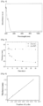
- diethyl zinc (DEZn) was used as the first precursor compound to deposit a thin film over an Si substrate and 4-mercapto phenol was used as the second precursor compound to form an organic-inorganic hybrid thin film over the diethyl zinc (DEZn) thin film according to the molecular layer deposition method before the process of forming the diethyl zinc (DEZn) by the first precursor compound, and while the thin film based on the second precursor compound was repeatedly formed, thicknesses of the thin film were measured and the results are shown in Figure 6 .
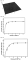
- the organic-inorganic hybrid thin film of 50 nm in the thickness prepared in Reference Example 2 was measured for its surface roughness with AFM, and the results are shown in Figure 7 .
- the average roughness measured was 2.2 A.
- TMA trimethyl aluminium
- TMA trimethyl aluminium
- Argon was used for both carrier gas and purging gas, and DEZn and 4-mercapto phenol were respectively evaporated at 20°C and 70°C.
- One cycle was achieved by exposure to DEZn for 2 seconds, purging with Ar for 10 seconds, exposure to 4-mercapto phenol for 2 seconds and purging with Ar for 50 seconds.
- the thin film was grown at the temperature of 80°C to 200°C and under a pressure of 300 mTorr.
- the organic-inorganic hybrid thin film according to the present invention has no absorption in the visible ray range.
- an organic-inorganic hybrid thin film was prepared in the same way as in Reference Example 3 above except that trimethyl aluminium (TMA) was used as its first precursor compound to deposit a trimethyl aluminium (TMA) thin film oven an Si substrate according to the molecular layer deposition method and then hydroquinone (HQ) was used as its second precursor compound.
- TMA trimethyl aluminium
- HQ hydroquinone
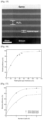
- trimethyl aluminium (TMA) was used as the first precursor compound to deposit a thin film over an Si substrate and 4-mercapto phenol was used as the second precursor compound to form an organic-inorganic hybrid thin film over the trimethyl aluminium (TMA) thin film according to the molecular layer deposition method before the process of forming the trimethyl aluminium (TMA) thin film by the first precursor compound, and while the thin film based on the second precursor compound was repeatedly formed, thicknesses of the thin film were measured and the results are shown in Figure 13 .
- the organic-inorganic hybrid thin film of 50 nm in the thickness prepared in Example 4 was measured for its surface roughness with AFM, and the results are shown in Figure 14 .
- the average roughness measured was 2.8 A.
- an Al 2 O 3 thin film was deposited over the organic-inorganic hybrid thin film according to the atomic layer deposition method, and such a process was repeated by controlling the ratio of the Al 2 O 3 thin film based on atomic layer deposition to the organic-inorganic hybrid thin film according to the present invention to prepare an organic-inorganic hybrid functional thin film.
- argon gas was used as carrier gas and purging gas, and trimethyl aluminium (TMA) and H 2 O were evaporated at normal temperature. Its cycle was achieved by exposure to TMA for 1 second, purging with Ar for 5 seconds, exposure to H 2 O for 1 second and purging with Ar for 5 seconds.
- TMA trimethyl aluminium
- H 2 O trimethyl aluminium
- the above thin film was grown at a temperature of 80°C under a pressure of 300 mTorr.
- Example 5 rates of pinhole formation inhibition were measured by varying the thickness of the organic-inorganic hybrid thin film, and the results are shown in Figure 16 and Figure 17 .
- the organic-inorganic hybrid thin film and encapsulting film according to the present invention include a new functional group so as to remain stable in air, they can be applied to various fields including nanos patterning for manufacturing semiconductors and electronic devices, chemical sensors and biosensors, nano tribology, surface modification, nano electronic machine systems (NEMS), micro electronic machine systems (MEMS) and non-volatile memory.
- NEMS nano electronic machine systems
- MEMS micro electronic machine systems
- the method for preparing functional thin film according to the present invention enables provision of a very stable organic-inorganic hybrid multi-layered molecular film in air by including a new functional group not used previously in its organic precursor when preparing the organic-inorganic hybrid thin film by alternately using inorganic precursor and organic precursor according to the molecular layer deposition method.
Landscapes
- Chemical & Material Sciences (AREA)
- Physics & Mathematics (AREA)
- Engineering & Computer Science (AREA)
- Organic Chemistry (AREA)
- Materials Engineering (AREA)
- General Physics & Mathematics (AREA)
- General Chemical & Material Sciences (AREA)
- Chemical Kinetics & Catalysis (AREA)
- Mechanical Engineering (AREA)
- Metallurgy (AREA)
- Microelectronics & Electronic Packaging (AREA)
- Nonlinear Science (AREA)
- Condensed Matter Physics & Semiconductors (AREA)
- Computer Hardware Design (AREA)
- Power Engineering (AREA)
- Optics & Photonics (AREA)
- Crystallography & Structural Chemistry (AREA)
- Mathematical Physics (AREA)
- Manufacturing & Machinery (AREA)
- Inorganic Chemistry (AREA)
- Spectroscopy & Molecular Physics (AREA)
- Chemical Vapour Deposition (AREA)
- Physical Vapour Deposition (AREA)
- Electroluminescent Light Sources (AREA)
- Laminated Bodies (AREA)
- Photovoltaic Devices (AREA)
- Formation Of Insulating Films (AREA)
- Inorganic Compounds Of Heavy Metals (AREA)
- Liquid Crystal (AREA)
- Oxygen, Ozone, And Oxides In General (AREA)
- Polymers With Sulfur, Phosphorus Or Metals In The Main Chain (AREA)
Applications Claiming Priority (2)
| Application Number | Priority Date | Filing Date | Title |
|---|---|---|---|
| KR1020130104463 | 2013-08-30 | ||
| PCT/KR2013/009909 WO2015030297A1 (ko) | 2013-08-30 | 2013-11-04 | 유무기 혼성 박막 및 이의 제조 방법 |
Publications (3)
| Publication Number | Publication Date |
|---|---|
| EP3040442A1 EP3040442A1 (en) | 2016-07-06 |
| EP3040442A4 EP3040442A4 (en) | 2017-04-12 |
| EP3040442B1 true EP3040442B1 (en) | 2024-02-14 |
Family
ID=52586830
Family Applications (2)
| Application Number | Title | Priority Date | Filing Date |
|---|---|---|---|
| EP13892196.0A Active EP3040442B1 (en) | 2013-08-30 | 2013-11-04 | Functional thin films comprising an hybrid organic/inorganic thin films and method of manufacturing same |
| EP13892719.9A Active EP3040443B1 (en) | 2013-08-30 | 2013-11-04 | Substrate structure and method of manufacturing same |
Family Applications After (1)
| Application Number | Title | Priority Date | Filing Date |
|---|---|---|---|
| EP13892719.9A Active EP3040443B1 (en) | 2013-08-30 | 2013-11-04 | Substrate structure and method of manufacturing same |
Country Status (12)
| Country | Link |
|---|---|
| US (2) | US9576876B2 (enExample) |
| EP (2) | EP3040442B1 (enExample) |
| JP (2) | JP6654753B2 (enExample) |
| KR (2) | KR20150026746A (enExample) |
| CN (2) | CN105745353B (enExample) |
| BR (2) | BR112016004476A2 (enExample) |
| CA (2) | CA2922612A1 (enExample) |
| MX (2) | MX389406B (enExample) |
| RU (2) | RU2672962C2 (enExample) |
| SG (2) | SG11201600923YA (enExample) |
| TW (2) | TWI606111B (enExample) |
| WO (2) | WO2015030297A1 (enExample) |
Families Citing this family (26)
| Publication number | Priority date | Publication date | Assignee | Title |
|---|---|---|---|---|
| RU2672962C2 (ru) * | 2013-08-30 | 2018-11-21 | Июкф-Хю (Индастри-Юниверсити-Кооперейшн Фаундейшн Ханян Юниверсити) | Структура подложки и способ ее изготовления |
| KR101816967B1 (ko) * | 2013-09-30 | 2018-01-09 | 주식회사 엘지화학 | 유기전자소자용 기판 및 이의 제조방법 |
| MX390409B (es) * | 2014-06-12 | 2025-03-20 | Basf Coatings Gmbh | Proceso para producir laminados orgánicos-inorgánicos flexibles. |
| WO2016150759A1 (en) * | 2015-03-25 | 2016-09-29 | Basf Coatings Gmbh | Process for producing flexible organic-inorganic laminates |
| US20190036077A1 (en) * | 2016-02-18 | 2019-01-31 | Sharp Kabushiki Kaisha | Method for producing organic el display device, and organic el display device |
| KR102586045B1 (ko) * | 2016-07-12 | 2023-10-10 | 삼성디스플레이 주식회사 | 디스플레이 장치 및 이의 제조 방법 |
| US20190040503A1 (en) * | 2017-08-03 | 2019-02-07 | Hrl Laboratories, Llc | Feedstocks for additive manufacturing, and methods of using the same |
| WO2019010696A1 (en) * | 2017-07-14 | 2019-01-17 | General Electric Company | METHOD FOR DEPOSITION LAYERED BY GAS PHASE MOLECULAR LAYER ON A MICROPOROUS SUPPORT |
| US10673046B2 (en) * | 2018-04-13 | 2020-06-02 | GM Global Technology Operations LLC | Separator for lithium metal based batteries |
| JP7451486B2 (ja) * | 2018-07-05 | 2024-03-18 | ビーエーエスエフ コーティングス ゲゼルシャフト ミット ベシュレンクテル ハフツング | 透明導電性フィルム |
| KR102224346B1 (ko) * | 2019-07-11 | 2021-03-05 | 한양대학교 산학협력단 | 유무기 하이브리드층, 이 층을 구비하는 유무기 적층체, 및 이 적층체를 가스 배리어로 구비하는 유기전자소자 |
| CN110508155B (zh) * | 2019-08-21 | 2021-09-03 | 南京大学 | 一种锌基无机-有机杂化纳米多孔分离膜的制备方法 |
| CN110635044B (zh) * | 2019-11-04 | 2021-07-06 | 吉林大学 | 一种有机金属卤化物钙钛矿太阳能电池的复合封装薄膜及其制备方法 |
| CN112410763A (zh) * | 2020-10-28 | 2021-02-26 | 武汉华星光电半导体显示技术有限公司 | 一种薄膜封装层,其制备方法及可折叠显示装置 |
| TWI824213B (zh) * | 2020-12-19 | 2023-12-01 | 逢甲大學 | 可撓式透明導電複合膜及其製造方法 |
| KR102558965B1 (ko) * | 2021-03-18 | 2023-07-25 | 한국과학기술연구원 | 신축성 표시 장치 및 신축성 표시 장치 제조 방법 |
| TW202311054A (zh) | 2021-05-06 | 2023-03-16 | 德商巴斯夫塗料有限責任公司 | 多層障壁膜、其製造及其於光伏打應用之用途 |
| WO2023018308A1 (ko) * | 2021-08-12 | 2023-02-16 | 한양대학교 산학협력단 | 분자선 구조를 갖는 다층 분자막 포토레지스트 및 이의 제조방법 |
| EP4386482A4 (en) * | 2021-08-12 | 2025-10-22 | Iucf Hyu | MULTILAYER MOLECULAR FILM PHOTOSENSITIVE RESIN HAVING MOLECULAR LINE STRUCTURE AND METHOD FOR PRODUCING SAME |
| KR102796366B1 (ko) * | 2022-01-13 | 2025-04-18 | 한양대학교 산학협력단 | 분자선 구조를 갖는 다층 분자막 포토레지스트의 제조방법 |
| CN115124727B (zh) * | 2022-07-08 | 2023-07-14 | 中国科学院山西煤炭化学研究所 | 一种mof薄膜的制备方法 |
| CN117845191A (zh) * | 2022-09-30 | 2024-04-09 | 华为技术有限公司 | 复合薄膜及其制备方法和应用 |
| CN120615105A (zh) | 2022-12-14 | 2025-09-09 | 巴斯夫涂料有限公司 | 多层阻挡膜涂覆的聚合物基底、其制造和在电子装置中的用途 |
| WO2024167351A1 (ko) * | 2023-02-10 | 2024-08-15 | 한양대학교 산학협력단 | 분자선 구조를 갖는 포지티브형의 다층 분자막 포토레지스트 |
| WO2024167360A1 (ko) * | 2023-02-10 | 2024-08-15 | 한양대학교 산학협력단 | 배위결합에 의해 가교가능한 분자선 구조를 갖는 다층 분자막 포토레지스트 |
| CN116794116A (zh) * | 2023-05-29 | 2023-09-22 | 南京大学 | 一种基于无机-有机杂化纳米多孔膜/半导体金属氧化物的薄膜氢气传感器及其制备方法 |
Citations (4)
| Publication number | Priority date | Publication date | Assignee | Title |
|---|---|---|---|---|
| US20040053431A1 (en) * | 2002-09-13 | 2004-03-18 | Industrial Technology Research Institute | Method of forming a flexible thin film transistor display device with a metal foil substrate |
| US20040161873A1 (en) * | 2002-11-25 | 2004-08-19 | Dimitrakopoulos Christos D. | Organic underlayers that improve the performance of organic semiconductors |
| KR20070084683A (ko) * | 2006-02-21 | 2007-08-27 | 국민대학교산학협력단 | 분자층 증착법 |
| WO2009002892A1 (en) * | 2007-06-22 | 2008-12-31 | The Regents Of The University Of Colorado | Protective coatings for organic electronic devices made using atomic layer deposition and molecular layer deposition techniques |
Family Cites Families (39)
| Publication number | Priority date | Publication date | Assignee | Title |
|---|---|---|---|---|
| RU2118402C1 (ru) * | 1994-05-17 | 1998-08-27 | Виктор Васильевич Дроботенко | Способ получения металлооксидных покрытий (его варианты) |
| JP2002053669A (ja) * | 2000-06-01 | 2002-02-19 | Osaka Organic Chem Ind Ltd | 多次元有機・無機複合体化合物およびその製造方法 |
| US6866949B2 (en) | 2002-03-08 | 2005-03-15 | Dai Nippon Printing Co., Ltd. | Substrate film, gas barrier film, and display using the same |
| JP2004231784A (ja) * | 2003-01-30 | 2004-08-19 | Konica Minolta Holdings Inc | 有機−無機ポリマーハイブリッドフィルム、その製造方法、該フィルムを用いたディスプレイ及びタッチパネル |
| US7229703B2 (en) | 2003-03-31 | 2007-06-12 | Dai Nippon Printing Co. Ltd. | Gas barrier substrate |
| CA2525622C (en) | 2003-05-16 | 2010-10-26 | Toppan Printing Co., Ltd. | Transparent gas barrier laminated film, and electroluminescent light-emiiting element, electroluminescent display device, and electrophoretic display panel using the same |
| US20050153077A1 (en) | 2003-12-03 | 2005-07-14 | Anthony Gedeon | Method of resisting contaminant build up and oxidation of vehicle surfaces and other surfaces |
| JP2005289885A (ja) * | 2004-03-31 | 2005-10-20 | Osaka Organic Chem Ind Ltd | 多次元有機・無機複合体化合物、複合焼成体およびこれらの製造方法 |
| JP2005297498A (ja) | 2004-04-16 | 2005-10-27 | Dainippon Printing Co Ltd | 可撓性基板およびそれを用いた有機デバイス |
| US7378157B2 (en) | 2004-06-28 | 2008-05-27 | Dai Nippon Printing Co., Ltd. | Gas barrier film, and display substrate and display using the same |
| KR101001441B1 (ko) * | 2004-08-17 | 2010-12-14 | 삼성전자주식회사 | 유무기 금속 하이브리드 물질 및 이를 포함하는 유기절연체 조성물 |
| NO20045674D0 (no) * | 2004-12-28 | 2004-12-28 | Uni I Oslo | Thin films prepared with gas phase deposition technique |
| JP2007185937A (ja) | 2005-12-12 | 2007-07-26 | Fujifilm Corp | 有機−無機ハイブリッド材料、ガスバリヤーフィルム及びその製造方法 |
| JP2007273094A (ja) | 2006-03-30 | 2007-10-18 | Toppan Printing Co Ltd | 有機エレクトロルミネッセンス素子およびその製造方法 |
| DE102006016280A1 (de) * | 2006-04-01 | 2007-10-04 | Pvflex Solar Gmbh | Glasloser Solarstrom-Modul mit flexiblen Dünnschicht-Zellen und Verfahren zu seiner Herstellung |
| JP2008087163A (ja) | 2006-09-29 | 2008-04-17 | Fujifilm Corp | ガスバリア性積層フィルム、およびそれを用いた画像表示素子 |
| US10092927B2 (en) | 2006-11-13 | 2018-10-09 | The Regents Of The University Of Colorado, A Body Corporate | Molecular layer deposition process for making organic or organic-inorganic polymers |
| JP2008218632A (ja) * | 2007-03-02 | 2008-09-18 | Fujifilm Corp | 電子デバイス |
| US8197942B2 (en) | 2007-03-23 | 2012-06-12 | Dai Nippon Printing Co., Ltd. | Gas barrier sheet |
| JP5127277B2 (ja) | 2007-04-05 | 2013-01-23 | 新日鉄住金マテリアルズ株式会社 | 表面平坦性絶縁膜形成用塗布溶液、表面平坦性絶縁膜被覆基材、及び表面平坦性絶縁膜被覆基材の製造方法 |
| JP5198131B2 (ja) | 2007-05-14 | 2013-05-15 | 富士フイルム株式会社 | バリアフィルムおよび素子 |
| JP5510766B2 (ja) | 2007-06-20 | 2014-06-04 | 大日本印刷株式会社 | イオンプレーティング用蒸発源材料の原料粉末、イオンプレーティング用蒸発源材料及びその製造方法、ガスバリア性シート及びその製造方法 |
| US20090021797A1 (en) * | 2007-07-17 | 2009-01-22 | Luciano Joseph W | All-In-One Device With Integrated Monitor |
| JP2010006039A (ja) | 2007-09-05 | 2010-01-14 | Fujifilm Corp | ガスバリアフィルムおよびガスバリアフィルムを用いて表示素子を封止する方法。 |
| US8067085B2 (en) | 2007-09-14 | 2011-11-29 | Fujifilm Corporation | Gas barrier film, and display device comprising the same |
| US7858144B2 (en) * | 2007-09-26 | 2010-12-28 | Eastman Kodak Company | Process for depositing organic materials |
| RU2462793C2 (ru) * | 2007-12-28 | 2012-09-27 | Юниверсите Де Ля Медитерране Экс-Марсель Ii | Гибридные нанокомпозиционные материалы |
| US8776238B2 (en) * | 2008-07-16 | 2014-07-08 | International Business Machines Corporation | Verifying certificate use |
| US8241749B2 (en) | 2008-09-11 | 2012-08-14 | Fujifilm Corporation | Barrier laminate, gas barrier film, and device using the same |
| JP2011046060A (ja) | 2009-08-26 | 2011-03-10 | Fujifilm Corp | ガスバリアフィルムおよびガスバリアフィルムの製造方法 |
| JP4821925B2 (ja) | 2009-11-27 | 2011-11-24 | 大日本印刷株式会社 | ガスバリア性フィルム、装置、及びガスバリア性フィルムの製造方法 |
| WO2011115147A1 (ja) * | 2010-03-17 | 2011-09-22 | コニカミノルタホールディングス株式会社 | 有機電子デバイスおよびその製造方法 |
| US20130017400A1 (en) | 2010-03-25 | 2013-01-17 | Toppan Printing Co., Ltd. | Gas barrier laminate and packaging |
| JP5598080B2 (ja) | 2010-05-17 | 2014-10-01 | 大日本印刷株式会社 | ガスバリア性シートの製造方法 |
| JP5913809B2 (ja) | 2011-01-05 | 2016-04-27 | リンテック株式会社 | 透明電極基板、その製造方法、該透明電極基板を有する電子デバイス及び太陽電池 |
| JP5752438B2 (ja) * | 2011-02-23 | 2015-07-22 | グンゼ株式会社 | ガスバリアフィルム |
| JP2014514981A (ja) * | 2011-05-16 | 2014-06-26 | エルジー・ケム・リミテッド | 多層プラスチック基板およびその製造方法 |
| KR101432737B1 (ko) | 2011-07-28 | 2014-08-22 | 한양대학교 산학협력단 | 유기-무기 혼성 박막 및 이의 제조 방법 |
| RU2672962C2 (ru) * | 2013-08-30 | 2018-11-21 | Июкф-Хю (Индастри-Юниверсити-Кооперейшн Фаундейшн Ханян Юниверсити) | Структура подложки и способ ее изготовления |
-
2013
- 2013-11-04 RU RU2016111694A patent/RU2672962C2/ru active
- 2013-11-04 JP JP2016538483A patent/JP6654753B2/ja active Active
- 2013-11-04 WO PCT/KR2013/009909 patent/WO2015030297A1/ko not_active Ceased
- 2013-11-04 US US14/413,754 patent/US9576876B2/en active Active
- 2013-11-04 BR BR112016004476A patent/BR112016004476A2/pt not_active Application Discontinuation
- 2013-11-04 CA CA2922612A patent/CA2922612A1/en not_active Abandoned
- 2013-11-04 CA CA2922615A patent/CA2922615A1/en not_active Abandoned
- 2013-11-04 SG SG11201600923YA patent/SG11201600923YA/en unknown
- 2013-11-04 MX MX2016002432A patent/MX389406B/es unknown
- 2013-11-04 WO PCT/KR2013/009910 patent/WO2015030298A1/ko not_active Ceased
- 2013-11-04 CN CN201380079249.XA patent/CN105745353B/zh active Active
- 2013-11-04 CN CN201380079150.XA patent/CN105723011B/zh active Active
- 2013-11-04 JP JP2016538482A patent/JP6286557B2/ja active Active
- 2013-11-04 EP EP13892196.0A patent/EP3040442B1/en active Active
- 2013-11-04 MX MX2016002433A patent/MX390737B/es unknown
- 2013-11-04 RU RU2016111693A patent/RU2670303C2/ru active
- 2013-11-04 US US14/915,562 patent/US10418300B2/en active Active
- 2013-11-04 BR BR112016004389-8A patent/BR112016004389B1/pt active IP Right Grant
- 2013-11-04 EP EP13892719.9A patent/EP3040443B1/en active Active
- 2013-11-04 SG SG11201600921XA patent/SG11201600921XA/en unknown
- 2013-12-02 TW TW102143967A patent/TWI606111B/zh active
- 2013-12-02 TW TW102144000A patent/TWI521083B/zh active
-
2014
- 2014-02-17 KR KR20140018154A patent/KR20150026746A/ko not_active Withdrawn
- 2014-02-18 KR KR1020140018212A patent/KR102289064B1/ko active Active
Patent Citations (4)
| Publication number | Priority date | Publication date | Assignee | Title |
|---|---|---|---|---|
| US20040053431A1 (en) * | 2002-09-13 | 2004-03-18 | Industrial Technology Research Institute | Method of forming a flexible thin film transistor display device with a metal foil substrate |
| US20040161873A1 (en) * | 2002-11-25 | 2004-08-19 | Dimitrakopoulos Christos D. | Organic underlayers that improve the performance of organic semiconductors |
| KR20070084683A (ko) * | 2006-02-21 | 2007-08-27 | 국민대학교산학협력단 | 분자층 증착법 |
| WO2009002892A1 (en) * | 2007-06-22 | 2008-12-31 | The Regents Of The University Of Colorado | Protective coatings for organic electronic devices made using atomic layer deposition and molecular layer deposition techniques |
Non-Patent Citations (3)
| Title |
|---|
| KATSUHIKO KANAIZUKA ET AL: "Construction of Highly Oriented Crystalline Surface Coordination Polymers Composed of Copper Dithiooxamide Complexes", JOURNAL OF THE AMERICAN CHEMICAL SOCIETY, vol. 130, no. 47, 26 November 2008 (2008-11-26), US, pages 15778 - 15779, XP055405115, ISSN: 0002-7863, DOI: 10.1021/ja806799t * |
| PREINER MICHAEL ET AL: "Creating large area molecular electronic junctions using atomic layer deposition", APPLIED PHYSICS LETTERS, A I P PUBLISHING LLC, US, vol. 92, no. 21, 27 May 2008 (2008-05-27), pages 213301 - 213301, XP012107279, ISSN: 0003-6951, DOI: 10.1063/1.2917870 * |
| ZHOU HAN ET AL: "Fabrication of organic interfacial layers by molecular layer deposition: Present status and future opportunities", J. VAC. SCI. TECHNOL. A J. VAC. SCI. TECHNOL. A, vol. 31, no. 31, 20 May 2013 (2013-05-20), pages 40801, XP055952627, Retrieved from the Internet <URL:https://avs.scitation.org/doi/pdf/10.1116/1.4804609> * |
Also Published As
Similar Documents
| Publication | Publication Date | Title |
|---|---|---|
| EP3040442B1 (en) | Functional thin films comprising an hybrid organic/inorganic thin films and method of manufacturing same | |
| Benelmekki et al. | Nanostructured thin films–background, preparation and relation to the technological revolution of the 21st century | |
| Bulusu et al. | Improving the stability of atomic layer deposited alumina films in aqueous environments with metal oxide capping layers | |
| KR101807459B1 (ko) | 결함-치유 환원된 그래핀 산화물 히터를 이용한 자가치유 고분자의 자가치유 방법 | |
| Marin et al. | Atomic layer deposition: state-of-the-art and research/industrial perspectives | |
| Pakkala et al. | Atomic layer deposition | |
| Wang et al. | Impact of different intermediate layers on the morphology and crystallinity of TiO2 grown on carbon nanotubes by atomic layer deposition | |
| Fallah Azad et al. | The effect of seed layer on optical and structural characteristics of ZnO nanorod arrays deposited by CBD method | |
| KR102450786B1 (ko) | 적층체 및 그 제조 방법 | |
| Shukla et al. | Structural properties and wettability of TiO2 nanorods | |
| WO2008111850A2 (en) | Synthesis of molecular metalorganic compounds | |
| KR20150026747A (ko) | 유무기 혼성 박막 및 이의 제조 방법 | |
| EP3531462A1 (en) | Transparent conductive film | |
| EP4222293A1 (en) | Silicon carbide thin films and vapor deposition methods thereof | |
| TWI814855B (zh) | 透明導電膜 | |
| JP6794994B2 (ja) | タッチパネルセンサーフィルム | |
| US20130337157A1 (en) | Method for synthesizing metal or metal oxide nanoparticles by liquid phase deposition on the surface of a substrate |
Legal Events
| Date | Code | Title | Description |
|---|---|---|---|
| PUAI | Public reference made under article 153(3) epc to a published international application that has entered the european phase |
Free format text: ORIGINAL CODE: 0009012 |
|
| 17P | Request for examination filed |
Effective date: 20160330 |
|
| AK | Designated contracting states |
Kind code of ref document: A1 Designated state(s): AL AT BE BG CH CY CZ DE DK EE ES FI FR GB GR HR HU IE IS IT LI LT LU LV MC MK MT NL NO PL PT RO RS SE SI SK SM TR |
|
| AX | Request for extension of the european patent |
Extension state: BA ME |
|
| DAX | Request for extension of the european patent (deleted) | ||
| A4 | Supplementary search report drawn up and despatched |
Effective date: 20170313 |
|
| RIC1 | Information provided on ipc code assigned before grant |
Ipc: C23C 16/00 20060101AFI20170307BHEP Ipc: C23C 16/448 20060101ALI20170307BHEP |
|
| STAA | Information on the status of an ep patent application or granted ep patent |
Free format text: STATUS: EXAMINATION IS IN PROGRESS |
|
| 17Q | First examination report despatched |
Effective date: 20170918 |
|
| RAP1 | Party data changed (applicant data changed or rights of an application transferred) |
Owner name: IUCF-HYU (INDUSTRY-UNIVERSITY COOPERATION FOUNDATION HANYANG UNIVERSITY) |
|
| GRAP | Despatch of communication of intention to grant a patent |
Free format text: ORIGINAL CODE: EPIDOSNIGR1 |
|
| STAA | Information on the status of an ep patent application or granted ep patent |
Free format text: STATUS: GRANT OF PATENT IS INTENDED |
|
| INTG | Intention to grant announced |
Effective date: 20231013 |
|
| GRAS | Grant fee paid |
Free format text: ORIGINAL CODE: EPIDOSNIGR3 |
|
| GRAA | (expected) grant |
Free format text: ORIGINAL CODE: 0009210 |
|
| STAA | Information on the status of an ep patent application or granted ep patent |
Free format text: STATUS: THE PATENT HAS BEEN GRANTED |
|
| AK | Designated contracting states |
Kind code of ref document: B1 Designated state(s): AL AT BE BG CH CY CZ DE DK EE ES FI FR GB GR HR HU IE IS IT LI LT LU LV MC MK MT NL NO PL PT RO RS SE SI SK SM TR |
|
| REG | Reference to a national code |
Ref country code: GB Ref legal event code: FG4D |
|
| REG | Reference to a national code |
Ref country code: CH Ref legal event code: EP |
|
| REG | Reference to a national code |
Ref country code: DE Ref legal event code: R096 Ref document number: 602013085299 Country of ref document: DE |
|
| REG | Reference to a national code |
Ref country code: IE Ref legal event code: FG4D |
|
| REG | Reference to a national code |
Ref country code: LT Ref legal event code: MG9D |
|
| REG | Reference to a national code |
Ref country code: NL Ref legal event code: MP Effective date: 20240214 |
|
| PG25 | Lapsed in a contracting state [announced via postgrant information from national office to epo] |
Ref country code: IS Free format text: LAPSE BECAUSE OF FAILURE TO SUBMIT A TRANSLATION OF THE DESCRIPTION OR TO PAY THE FEE WITHIN THE PRESCRIBED TIME-LIMIT Effective date: 20240614 |
|
| PG25 | Lapsed in a contracting state [announced via postgrant information from national office to epo] |
Ref country code: LT Free format text: LAPSE BECAUSE OF FAILURE TO SUBMIT A TRANSLATION OF THE DESCRIPTION OR TO PAY THE FEE WITHIN THE PRESCRIBED TIME-LIMIT Effective date: 20240214 |
|
| PG25 | Lapsed in a contracting state [announced via postgrant information from national office to epo] |
Ref country code: GR Free format text: LAPSE BECAUSE OF FAILURE TO SUBMIT A TRANSLATION OF THE DESCRIPTION OR TO PAY THE FEE WITHIN THE PRESCRIBED TIME-LIMIT Effective date: 20240515 |
|
| REG | Reference to a national code |
Ref country code: AT Ref legal event code: MK05 Ref document number: 1657072 Country of ref document: AT Kind code of ref document: T Effective date: 20240214 |
|
| PG25 | Lapsed in a contracting state [announced via postgrant information from national office to epo] |
Ref country code: RS Free format text: LAPSE BECAUSE OF FAILURE TO SUBMIT A TRANSLATION OF THE DESCRIPTION OR TO PAY THE FEE WITHIN THE PRESCRIBED TIME-LIMIT Effective date: 20240514 Ref country code: NL Free format text: LAPSE BECAUSE OF FAILURE TO SUBMIT A TRANSLATION OF THE DESCRIPTION OR TO PAY THE FEE WITHIN THE PRESCRIBED TIME-LIMIT Effective date: 20240214 Ref country code: HR Free format text: LAPSE BECAUSE OF FAILURE TO SUBMIT A TRANSLATION OF THE DESCRIPTION OR TO PAY THE FEE WITHIN THE PRESCRIBED TIME-LIMIT Effective date: 20240214 |
|
| PG25 | Lapsed in a contracting state [announced via postgrant information from national office to epo] |
Ref country code: ES Free format text: LAPSE BECAUSE OF FAILURE TO SUBMIT A TRANSLATION OF THE DESCRIPTION OR TO PAY THE FEE WITHIN THE PRESCRIBED TIME-LIMIT Effective date: 20240214 |
|
| PG25 | Lapsed in a contracting state [announced via postgrant information from national office to epo] |
Ref country code: AT Free format text: LAPSE BECAUSE OF FAILURE TO SUBMIT A TRANSLATION OF THE DESCRIPTION OR TO PAY THE FEE WITHIN THE PRESCRIBED TIME-LIMIT Effective date: 20240214 |
|
| PG25 | Lapsed in a contracting state [announced via postgrant information from national office to epo] |
Ref country code: RS Free format text: LAPSE BECAUSE OF FAILURE TO SUBMIT A TRANSLATION OF THE DESCRIPTION OR TO PAY THE FEE WITHIN THE PRESCRIBED TIME-LIMIT Effective date: 20240514 Ref country code: NO Free format text: LAPSE BECAUSE OF FAILURE TO SUBMIT A TRANSLATION OF THE DESCRIPTION OR TO PAY THE FEE WITHIN THE PRESCRIBED TIME-LIMIT Effective date: 20240514 Ref country code: NL Free format text: LAPSE BECAUSE OF FAILURE TO SUBMIT A TRANSLATION OF THE DESCRIPTION OR TO PAY THE FEE WITHIN THE PRESCRIBED TIME-LIMIT Effective date: 20240214 Ref country code: LT Free format text: LAPSE BECAUSE OF FAILURE TO SUBMIT A TRANSLATION OF THE DESCRIPTION OR TO PAY THE FEE WITHIN THE PRESCRIBED TIME-LIMIT Effective date: 20240214 Ref country code: IS Free format text: LAPSE BECAUSE OF FAILURE TO SUBMIT A TRANSLATION OF THE DESCRIPTION OR TO PAY THE FEE WITHIN THE PRESCRIBED TIME-LIMIT Effective date: 20240614 Ref country code: HR Free format text: LAPSE BECAUSE OF FAILURE TO SUBMIT A TRANSLATION OF THE DESCRIPTION OR TO PAY THE FEE WITHIN THE PRESCRIBED TIME-LIMIT Effective date: 20240214 Ref country code: GR Free format text: LAPSE BECAUSE OF FAILURE TO SUBMIT A TRANSLATION OF THE DESCRIPTION OR TO PAY THE FEE WITHIN THE PRESCRIBED TIME-LIMIT Effective date: 20240515 Ref country code: FI Free format text: LAPSE BECAUSE OF FAILURE TO SUBMIT A TRANSLATION OF THE DESCRIPTION OR TO PAY THE FEE WITHIN THE PRESCRIBED TIME-LIMIT Effective date: 20240214 Ref country code: ES Free format text: LAPSE BECAUSE OF FAILURE TO SUBMIT A TRANSLATION OF THE DESCRIPTION OR TO PAY THE FEE WITHIN THE PRESCRIBED TIME-LIMIT Effective date: 20240214 Ref country code: BG Free format text: LAPSE BECAUSE OF FAILURE TO SUBMIT A TRANSLATION OF THE DESCRIPTION OR TO PAY THE FEE WITHIN THE PRESCRIBED TIME-LIMIT Effective date: 20240214 Ref country code: AT Free format text: LAPSE BECAUSE OF FAILURE TO SUBMIT A TRANSLATION OF THE DESCRIPTION OR TO PAY THE FEE WITHIN THE PRESCRIBED TIME-LIMIT Effective date: 20240214 |
|
| PG25 | Lapsed in a contracting state [announced via postgrant information from national office to epo] |
Ref country code: PT Free format text: LAPSE BECAUSE OF FAILURE TO SUBMIT A TRANSLATION OF THE DESCRIPTION OR TO PAY THE FEE WITHIN THE PRESCRIBED TIME-LIMIT Effective date: 20240614 Ref country code: PL Free format text: LAPSE BECAUSE OF FAILURE TO SUBMIT A TRANSLATION OF THE DESCRIPTION OR TO PAY THE FEE WITHIN THE PRESCRIBED TIME-LIMIT Effective date: 20240214 |
|
| PG25 | Lapsed in a contracting state [announced via postgrant information from national office to epo] |
Ref country code: SE Free format text: LAPSE BECAUSE OF FAILURE TO SUBMIT A TRANSLATION OF THE DESCRIPTION OR TO PAY THE FEE WITHIN THE PRESCRIBED TIME-LIMIT Effective date: 20240214 Ref country code: PT Free format text: LAPSE BECAUSE OF FAILURE TO SUBMIT A TRANSLATION OF THE DESCRIPTION OR TO PAY THE FEE WITHIN THE PRESCRIBED TIME-LIMIT Effective date: 20240614 Ref country code: PL Free format text: LAPSE BECAUSE OF FAILURE TO SUBMIT A TRANSLATION OF THE DESCRIPTION OR TO PAY THE FEE WITHIN THE PRESCRIBED TIME-LIMIT Effective date: 20240214 Ref country code: LV Free format text: LAPSE BECAUSE OF FAILURE TO SUBMIT A TRANSLATION OF THE DESCRIPTION OR TO PAY THE FEE WITHIN THE PRESCRIBED TIME-LIMIT Effective date: 20240214 |
|
| PG25 | Lapsed in a contracting state [announced via postgrant information from national office to epo] |
Ref country code: DK Free format text: LAPSE BECAUSE OF FAILURE TO SUBMIT A TRANSLATION OF THE DESCRIPTION OR TO PAY THE FEE WITHIN THE PRESCRIBED TIME-LIMIT Effective date: 20240214 |
|
| PG25 | Lapsed in a contracting state [announced via postgrant information from national office to epo] |
Ref country code: SM Free format text: LAPSE BECAUSE OF FAILURE TO SUBMIT A TRANSLATION OF THE DESCRIPTION OR TO PAY THE FEE WITHIN THE PRESCRIBED TIME-LIMIT Effective date: 20240214 |
|
| PG25 | Lapsed in a contracting state [announced via postgrant information from national office to epo] |
Ref country code: CZ Free format text: LAPSE BECAUSE OF FAILURE TO SUBMIT A TRANSLATION OF THE DESCRIPTION OR TO PAY THE FEE WITHIN THE PRESCRIBED TIME-LIMIT Effective date: 20240214 Ref country code: EE Free format text: LAPSE BECAUSE OF FAILURE TO SUBMIT A TRANSLATION OF THE DESCRIPTION OR TO PAY THE FEE WITHIN THE PRESCRIBED TIME-LIMIT Effective date: 20240214 |
|
| PG25 | Lapsed in a contracting state [announced via postgrant information from national office to epo] |
Ref country code: SK Free format text: LAPSE BECAUSE OF FAILURE TO SUBMIT A TRANSLATION OF THE DESCRIPTION OR TO PAY THE FEE WITHIN THE PRESCRIBED TIME-LIMIT Effective date: 20240214 |
|
| PG25 | Lapsed in a contracting state [announced via postgrant information from national office to epo] |
Ref country code: SM Free format text: LAPSE BECAUSE OF FAILURE TO SUBMIT A TRANSLATION OF THE DESCRIPTION OR TO PAY THE FEE WITHIN THE PRESCRIBED TIME-LIMIT Effective date: 20240214 Ref country code: SK Free format text: LAPSE BECAUSE OF FAILURE TO SUBMIT A TRANSLATION OF THE DESCRIPTION OR TO PAY THE FEE WITHIN THE PRESCRIBED TIME-LIMIT Effective date: 20240214 Ref country code: RO Free format text: LAPSE BECAUSE OF FAILURE TO SUBMIT A TRANSLATION OF THE DESCRIPTION OR TO PAY THE FEE WITHIN THE PRESCRIBED TIME-LIMIT Effective date: 20240214 Ref country code: EE Free format text: LAPSE BECAUSE OF FAILURE TO SUBMIT A TRANSLATION OF THE DESCRIPTION OR TO PAY THE FEE WITHIN THE PRESCRIBED TIME-LIMIT Effective date: 20240214 Ref country code: DK Free format text: LAPSE BECAUSE OF FAILURE TO SUBMIT A TRANSLATION OF THE DESCRIPTION OR TO PAY THE FEE WITHIN THE PRESCRIBED TIME-LIMIT Effective date: 20240214 Ref country code: CZ Free format text: LAPSE BECAUSE OF FAILURE TO SUBMIT A TRANSLATION OF THE DESCRIPTION OR TO PAY THE FEE WITHIN THE PRESCRIBED TIME-LIMIT Effective date: 20240214 |
|
| REG | Reference to a national code |
Ref country code: DE Ref legal event code: R097 Ref document number: 602013085299 Country of ref document: DE |
|
| PG25 | Lapsed in a contracting state [announced via postgrant information from national office to epo] |
Ref country code: IT Free format text: LAPSE BECAUSE OF FAILURE TO SUBMIT A TRANSLATION OF THE DESCRIPTION OR TO PAY THE FEE WITHIN THE PRESCRIBED TIME-LIMIT Effective date: 20240214 |
|
| PLBE | No opposition filed within time limit |
Free format text: ORIGINAL CODE: 0009261 |
|
| STAA | Information on the status of an ep patent application or granted ep patent |
Free format text: STATUS: NO OPPOSITION FILED WITHIN TIME LIMIT |
|
| PG25 | Lapsed in a contracting state [announced via postgrant information from national office to epo] |
Ref country code: IT Free format text: LAPSE BECAUSE OF FAILURE TO SUBMIT A TRANSLATION OF THE DESCRIPTION OR TO PAY THE FEE WITHIN THE PRESCRIBED TIME-LIMIT Effective date: 20240214 |
|
| PGFP | Annual fee paid to national office [announced via postgrant information from national office to epo] |
Ref country code: DE Payment date: 20241007 Year of fee payment: 12 |
|
| 26N | No opposition filed |
Effective date: 20241115 |
|
| PG25 | Lapsed in a contracting state [announced via postgrant information from national office to epo] |
Ref country code: SI Free format text: LAPSE BECAUSE OF FAILURE TO SUBMIT A TRANSLATION OF THE DESCRIPTION OR TO PAY THE FEE WITHIN THE PRESCRIBED TIME-LIMIT Effective date: 20240214 |
|
| REG | Reference to a national code |
Ref country code: CH Ref legal event code: PL |
|
| PG25 | Lapsed in a contracting state [announced via postgrant information from national office to epo] |
Ref country code: MC Free format text: LAPSE BECAUSE OF FAILURE TO SUBMIT A TRANSLATION OF THE DESCRIPTION OR TO PAY THE FEE WITHIN THE PRESCRIBED TIME-LIMIT Effective date: 20240214 |
|
| PG25 | Lapsed in a contracting state [announced via postgrant information from national office to epo] |
Ref country code: LU Free format text: LAPSE BECAUSE OF NON-PAYMENT OF DUE FEES Effective date: 20241104 |
|
| REG | Reference to a national code |
Ref country code: CH Ref legal event code: PL |
|
| PG25 | Lapsed in a contracting state [announced via postgrant information from national office to epo] |
Ref country code: CH Free format text: LAPSE BECAUSE OF NON-PAYMENT OF DUE FEES Effective date: 20241130 |
|
| REG | Reference to a national code |
Ref country code: BE Ref legal event code: MM Effective date: 20241130 |
|
| PG25 | Lapsed in a contracting state [announced via postgrant information from national office to epo] |
Ref country code: BE Free format text: LAPSE BECAUSE OF NON-PAYMENT OF DUE FEES Effective date: 20241130 |
|
| PGFP | Annual fee paid to national office [announced via postgrant information from national office to epo] |
Ref country code: GB Payment date: 20250922 Year of fee payment: 13 |
|
| PGFP | Annual fee paid to national office [announced via postgrant information from national office to epo] |
Ref country code: FR Payment date: 20250925 Year of fee payment: 13 |
|
| PG25 | Lapsed in a contracting state [announced via postgrant information from national office to epo] |
Ref country code: IE Free format text: LAPSE BECAUSE OF NON-PAYMENT OF DUE FEES Effective date: 20241104 |