EP2571255A1 - A/D converter and solid-state imaging apparatus - Google Patents
A/D converter and solid-state imaging apparatus Download PDFInfo
- Publication number
- EP2571255A1 EP2571255A1 EP12182125A EP12182125A EP2571255A1 EP 2571255 A1 EP2571255 A1 EP 2571255A1 EP 12182125 A EP12182125 A EP 12182125A EP 12182125 A EP12182125 A EP 12182125A EP 2571255 A1 EP2571255 A1 EP 2571255A1
- Authority
- EP
- European Patent Office
- Prior art keywords
- signal
- input terminal
- inverting input
- comparator
- analog signal
- Prior art date
- Legal status (The legal status is an assumption and is not a legal conclusion. Google has not performed a legal analysis and makes no representation as to the accuracy of the status listed.)
- Withdrawn
Links
- 238000003384 imaging method Methods 0.000 title claims description 38
- 239000003990 capacitor Substances 0.000 claims abstract description 91
- 238000006243 chemical reaction Methods 0.000 claims description 17
- 238000005070 sampling Methods 0.000 claims description 8
- 230000007423 decrease Effects 0.000 description 9
- 238000010586 diagram Methods 0.000 description 9
- 238000009792 diffusion process Methods 0.000 description 8
- 238000000034 method Methods 0.000 description 4
- 101000690100 Homo sapiens U1 small nuclear ribonucleoprotein 70 kDa Proteins 0.000 description 3
- 101100257820 Neurospora crassa (strain ATCC 24698 / 74-OR23-1A / CBS 708.71 / DSM 1257 / FGSC 987) ssp-1 gene Proteins 0.000 description 3
- 102100024121 U1 small nuclear ribonucleoprotein 70 kDa Human genes 0.000 description 3
- 230000004048 modification Effects 0.000 description 3
- 238000012986 modification Methods 0.000 description 3
- 230000003252 repetitive effect Effects 0.000 description 3
- 101100148606 Caenorhabditis elegans pst-1 gene Proteins 0.000 description 2
- 101100259462 Caenorhabditis elegans snt-1 gene Proteins 0.000 description 2
- 101100352663 Mus musculus Pnp gene Proteins 0.000 description 2
- 101100013480 Rattus norvegicus Frs3 gene Proteins 0.000 description 2
- 101100301987 Rattus norvegicus Rida gene Proteins 0.000 description 2
- 230000000694 effects Effects 0.000 description 2
- 101150108487 pst2 gene Proteins 0.000 description 2
- 230000002411 adverse Effects 0.000 description 1
- 230000008878 coupling Effects 0.000 description 1
- 238000010168 coupling process Methods 0.000 description 1
- 238000005859 coupling reaction Methods 0.000 description 1
- 239000011159 matrix material Substances 0.000 description 1
- -1 that is Substances 0.000 description 1
Images


Classifications
-
- H—ELECTRICITY
- H04—ELECTRIC COMMUNICATION TECHNIQUE
- H04N—PICTORIAL COMMUNICATION, e.g. TELEVISION
- H04N25/00—Circuitry of solid-state image sensors [SSIS]; Control thereof
- H04N25/70—SSIS architectures; Circuits associated therewith
- H04N25/76—Addressed sensors, e.g. MOS or CMOS sensors
- H04N25/78—Readout circuits for addressed sensors, e.g. output amplifiers or A/D converters
-
- H—ELECTRICITY
- H04—ELECTRIC COMMUNICATION TECHNIQUE
- H04N—PICTORIAL COMMUNICATION, e.g. TELEVISION
- H04N25/00—Circuitry of solid-state image sensors [SSIS]; Control thereof
- H04N25/70—SSIS architectures; Circuits associated therewith
- H04N25/71—Charge-coupled device [CCD] sensors; Charge-transfer registers specially adapted for CCD sensors
- H04N25/75—Circuitry for providing, modifying or processing image signals from the pixel array
-
- H—ELECTRICITY
- H04—ELECTRIC COMMUNICATION TECHNIQUE
- H04N—PICTORIAL COMMUNICATION, e.g. TELEVISION
- H04N25/00—Circuitry of solid-state image sensors [SSIS]; Control thereof
- H04N25/70—SSIS architectures; Circuits associated therewith
- H04N25/76—Addressed sensors, e.g. MOS or CMOS sensors
- H04N25/77—Pixel circuitry, e.g. memories, A/D converters, pixel amplifiers, shared circuits or shared components
- H04N25/772—Pixel circuitry, e.g. memories, A/D converters, pixel amplifiers, shared circuits or shared components comprising A/D, V/T, V/F, I/T or I/F converters
-
- G—PHYSICS
- G02—OPTICS
- G02F—OPTICAL DEVICES OR ARRANGEMENTS FOR THE CONTROL OF LIGHT BY MODIFICATION OF THE OPTICAL PROPERTIES OF THE MEDIA OF THE ELEMENTS INVOLVED THEREIN; NON-LINEAR OPTICS; FREQUENCY-CHANGING OF LIGHT; OPTICAL LOGIC ELEMENTS; OPTICAL ANALOGUE/DIGITAL CONVERTERS
- G02F7/00—Optical analogue/digital converters
Definitions
- the present invention relates to an A/D converter and solid-state imaging apparatus.
- a technique which arranges A/D converters in correspondence with columns of pixels arranged in an array and converts signals from the respective pixels into digital data in a solid-state imaging apparatus is known.
- offset voltages of comparators included in the respective A/D converters are different, an A/D conversion period has to be set in consideration of a maximum value of the offset voltages.
- U.S. Patent No. 7,671,908 has proposed a technique for correcting an offset voltage by feeding back an output of the comparator included in each individual A/D converter to an input of that comparator.
- the present invention in its first aspect provides an A/D converter as specified in claims 1 to 7.
- the present invention in its second aspect provides a solid-state imaging apparatus as specified in claims 8 to 11.
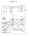
- Fig. 1 is a block diagram for explaining an example of the arrangement of a solid-state imaging apparatus 100 according to an embodiment of the present invention
- Fig. 2 is a circuit diagram for explaining an example of the arrangements of a pixel 111 and amplifier circuit 120 according to the embodiment of the present invention
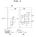
- Fig. 3 is a circuit diagram for explaining an example of the arrangement of an A/D converter 300 according to the embodiment of the present invention.
- Fig. 4 is a timing chart for explaining an example of the operation of the solid-state imaging apparatus 100 according to the embodiment of the present invention.
- Fig. 5 is a circuit diagram for explaining an example of the arrangement of an A/D converter 500 according to the embodiment of the present invention.
- Fig. 6 is a timing chart for explaining another example of the operation of the solid-state imaging apparatus 100 according to the embodiment of the present invention.
- Fig. 7 is a circuit diagram for explaining an example of the arrangement of an A/D converter 700 according to the embodiment of the present invention.
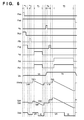
- Fig. 8 is a timing chart for explaining still another example of the operation of the solid-state imaging apparatus 100 according to the embodiment of the present invention.
- the solid-state imaging apparatus 100 is, for example, a CMOS image sensor, which photoelectrically converts incoming light indicating an object image, and externally outputs an electrical signal obtained by the photoelectric conversion as digital data.
- the solid-state imaging apparatus 100 can include an analog signal generator 110 including a pixel array formed by arranging a plurality of pixels 111 in a matrix.
- Fig. 1 illustrates four pixels 111 for the sake of simplicity, but the number of pixels 111 is not limited to this. Each pixel 111 photoelectrically converts incoming light to the solid-state imaging apparatus 100 into an analog signal.
- the solid-state imaging apparatus 100 can further include a vertical scanning circuit 140.
- the vertical scanning circuit 140 supplies a driving pulse signal in turn to row selection lines 112 arranged in correspondence with respective pixel rows.
- analog signals are read out from respective pixels 111 included in the corresponding pixel row onto column signal lines 113.
- This embodiment will handle a case in which a reset-level signal of the pixel 111 and a signal obtained by superimposing a signal according to a charge generated by the photoelectric conversion on the reset-level signal are read out from the pixel 111. A difference between these signals represents an effective pixel value.
- the analog signal generator 110 outputs, based on these signals, a noise signal at a reset timing and a pixel signal depending on a charge obtained by the photoelectric conversion for each pixel 111.
- the analog signal generator 110 can further include amplifier circuits 120 for respective column signal lines 113. Each amplifier circuit 120 amplifies the analog signal input from the corresponding pixel 111 via the column signal line 113, and supplies the amplified analog signal to a corresponding A/D converter 130.
- the solid-state imaging apparatus 100 can further include A/D converters 130 in correspondence with respective column signal lines 113. Each A/D converter converts the input analog signal into digital data, and outputs the digital data.
- the solid-state imaging apparatus 100 can further include a ramp signal generator 170 and counter 180.
- the ramp signal generator 170 generates a ramp signal Vramp which changes in a slope pattern along with an elapse of time, and supplies the generated ramp signal Vramp to the respective A/D converters 130 via a ramp signal line 171.
- a signal source for generating another reference signal which changes temporally in place of the ramp signal may be used as the ramp signal generator 170. In this case, this reference signal is supplied to the respective A/D converters 130 via a reference signal supply line.
- the reference signal can use an arbitrary signal as long as it monotonically changes along with an elapse of time.
- An example of the reference signal includes a signal which changes step by step along with an elapse of time in addition to the aforementioned ramp signal.
- “monotonic change” means a change in potential without increasing in case of, for example, a monotonic decrease.
- the counter 180 supplies a count value Cnt to the respective A/D converters 130 via a count data line 181.
- the counter 180 for example, a gray counter or binary counter may be used, and the counter 180 may have an up-down function. This embodiment will handle an example in which the plurality of A/D converters 130 share the ramp signal generator 170 and counter 180. Alternatively, each A/D converter 130 may have these components.
- the solid-state imaging apparatus 100 can further include a horizontal scanning circuit 150 and signal processor 190.
- the horizontal scanning circuit 150 transfers digital data output from the A/D converters 130 onto a digital signal line 191 for respective columns. Digital data transferred onto the digital signal line 191 is supplied to the signal processor 190.
- digital data corresponding to a noise signal and that corresponding to a pixel signal are read out in turn on the digital signal line 191.
- the signal processor 190 subtracts the digital data corresponding to the noise signal from that corresponding to the pixel signal, and externally outputs an effective pixel value.
- the solid-state imaging apparatus 100 can further include a timing controller 195 which supplies pulse signals to the aforementioned components to control the operation of the solid-state imaging apparatus 100.
- Fig. 1 does not illustrate any signal lines used to transmit the pulse signals from the timing controller 195 to the respective components.
- the pulse signals supplied from the timing controller 195 will be described in detail later using timing charts to be described later.
- the solid-state imaging apparatus 100 since the solid-state imaging apparatus 100 includes the amplifier circuits 120, the influences of noise components generated by the A/D converters 130 can be reduced.
- a modification of the solid-state imaging apparatus 100 may not include any amplifier circuit 120, and analog signals from the pixels 111 may be directly supplied to the A/D converters 130 via the column signal lines 113.
- Another modification of the solid-state imaging apparatus 100 may include CDS circuits in place of the amplifier circuits 120, and each CDS circuit may supply an analog signal obtained by subtracting a reset-level signal from a signal according to a charge generated by the pixel to the A/D converter 130.
- Each A/D converter converts this analog signal into digital data
- the horizontal scanning circuit 150 transfers the digital data corresponding to a pixel value of each pixel 111 to the signal processor 190.
- the amplifier circuits 120, A/D converters 130, and horizontal scanning circuit 150 are arranged on one side of the pixel array. Alternatively, these components may be arranged on both the sides of the pixel array, and data may be distributed to the components on either one side for respective pixel columns.
- the pixel 111 and amplifier circuit 120 may have arbitrary arrangements as long as an analog signal required for calculating a pixel value of that pixel 111 can be supplied to the A/D converter 130.
- the pixel 111 includes a photodiode PD required to execute the photoelectric conversion and a plurality of transistors.
- the photodiode PD is connected to a floating diffusion FD via a transfer transistor Ttx.
- the floating diffusion FD is also connected to a voltage source VDD via a reset transistor Tres, and to a gate electrode of an amplifier transistor Tamp.
- a first main electrode of the amplifier transistor Tamp is connected to the voltage source VDD, and a second main electrode of the amplifier transistor Tamp is connected to the column signal line 113 via a selection transistor Tsel.
- a gate electrode of the selection transistor Tsel is connected to the row selection line 112. When the selection transistor Tsel is turned on, the amplifier transistor Tamp operates as a source-follower circuit together with a constant current source Icnst inserted in the column signal line 113.
- the amplifier circuit 120 includes illustrated circuit elements, and configures an inverting amplifier.
- a non-inverting input terminal of an amplifier AMP is connected to the column signal line 113 via a clamp capacitor Co, and Vcor is supplied to an inverting input terminal of the amplifier AMP.
- An output terminal of the amplifier AMP is connected to the A/D converter 130.
- a parallel circuit of a feedback capacitor Cf and switch Scor is connected between the non-inverting input terminal and output terminal of the amplifier AMP.
- an offset of the amplifier circuit 120 is output from the analog signal generator 110.
- a signal from which a reset-level signal is removed is output from the analog signal generator 110.
- the analog signal generator 110 outputs a reset-level signal of the pixel as a noise signal, and a signal obtained by superimposing a signal according to a charge generated by the pixel on the reset-level signal as a pixel signal.
- noise components generated as a result of resetting of the floating diffusion FD can be reduced.
- the A/D converter 300 can include an input terminal IN, output terminals OUTn and OUTs, comparison circuit 320, and output circuit 330.
- the comparison circuit 320 executes comparison based on an analog signal input to the input terminal IN and the ramp signal Vramp supplied from the ramp signal line 171, and outputs an output signal Vout of a level according to that comparison result.
- the output circuit 330 outputs digital data based on the output signal Vout from the comparison circuit 320 and the count value Cnt supplied from the counter 180 from the output terminal OUTn or OUTs.
- the comparison circuit 320 can include a comparator CMP, capacitor Coff, and switch Sfb.
- the capacitor Coff can function as a correction capacitor which corrects an offset of the comparator CMP.
- the comparator CMP can be a differential input comparator having a non-inverting input terminal and inverting input terminal.
- the non-inverting input terminal ("+" terminal in Fig. 3 ) of the comparator CMP is connected to the input terminal IN
- the inverting input terminal (“-" terminal in Fig. 3 ) of the comparator CMP is connected to a first electrode (upper electrode in Fig. 3 ) of the capacitor Coff.
- a second electrode (lower electrode in Fig. 3 ) of the capacitor Coff is connected to the ramp signal line 171.
- the switch Sfb connects the output terminal and inverting input terminal of the comparator CMP.
- the output circuit 330 can include four latch circuits Ln1, Ln2, Ls1, and Ls2, which store digital data. Both of a D terminal of the latch circuit Ln1 and that of the latch circuit Ls1 are connected to the count data line 181.
- a G terminal of the latch circuit Ln1 is connected to the output line of the comparison circuit 320 via a switch Snl, and a G terminal of the latch circuit Ls1 is connected to the output line of the comparison circuit 320 via a switch Ssl.
- a Q terminal of the latch circuit Ln1 is connected to a D terminal of the latch circuit Ln2, and a Q terminal of the latch circuit Ls1 is connected to a D terminal of the latch circuit Ls2.
- Both of a G terminal of the latch circuit Ln2 and that of the latch circuit Ls2 are connected to a signal line 331.
- a Q terminal of the latch circuit Ln2 is connected to the output terminal OUTn, and a Q terminal of the latch circuit Ls2 is connected to the output terminal OUTs. Since an inverting circuit is connected to the G terminals of the latch circuits Ln1 and Ls1, when the output from the comparison circuit 320 is at L level, data at the D terminals are output from the Q terminals.
- Respective pulse signals shown in Fig. 4 are generated by the timing controller 195, and are supplied to respective circuit elements in the solid-state imaging apparatus 100. That is, the timing controller 195 can control the operations of the respective components of the solid-state imaging apparatus 100.
- the operation of the pixel 111 of one row will be explained, but the same applies to the pixel 111 of another row.
- reference symbol Vpin denotes a voltage of the non-inverting input terminal of the comparator CMP; and Vnin, a voltage of the inverting input terminal of the comparator CMP.
- a noise signal Vn from the pixel 111 is supplied to the A/D converter 300 during a period T1
- an offset voltage Voff of the comparator CMP is held in the capacitor Coff during a period T2
- the noise signal Vn is A/D-converted during a period T3.
- a pixel signal Vs from the pixel 111 is supplied to the A/D converter 300 during a period T4, and is A/D-converted during a period T5.
- pulse signals Pres, Psel, and Pcor respectively go H (High level), thus turning on the reset transistor Tres, selection transistor Tsel, and switch Scor.
- the floating diffusion FD is reset.
- the amplifier transistor Tamp operates as a source-follower, and a reset-level signal of the floating diffusion FD is read out onto the column signal line 113.
- the pulse signal Pcor goes L (Low level)
- the clamp capacitor Co holds a potential difference between Vcor and the pixel output.
- the output of the amplifier circuit 120 at this time is supplied to the input terminal IN of the A/D converter 300 as the noise signal Vn (first analog signal). For this reason, the voltage Vpin of the non-inverting input terminal of the comparator CMP also becomes equal to Vn.
- the noise signal Vn contains an offset of the amplifier circuit 120.
- the noise signal Vn is continuously supplied until a pulse signal Ptx goes H.
- a pulse signal Pfb goes H, and the switch Sfb is turned on.
- the inverting input terminal and output terminal of the comparator CMP are short-circuited, and the comparator CMP operates as a voltage-follower. Since the voltage Vpin of the non-inverting input terminal of the comparator CMP is Vn, the voltage Vout of the output terminal is Vn + Voff, and the voltage Vnin of the inverting input terminal is also Vn + Voff. Also, the potential of the first electrode of the capacitor Coff is Vn + Voff. During the period T2, since the voltage of the ramp signal line 171 is Vref, the potential of the second electrode of the capacitor Coff is Vref.
- the pulse signal Pfb goes L, the switch Sfb is turned off, and the capacitor Coff holds Vn + Voff - Vref as a voltage across its two electrodes. Then, the A/D converter 130 is set in a ready state (that can correspond to a first state).
- the ramp signal generator 170 changes a voltage to be supplied onto the ramp signal line 171 to Vstn in accordance with a pulse signal (not shown) from the timing controller 195.
- the potential of the second electrode of the capacitor Coff becomes Vstn
- the potential of the first electrode of the capacitor Coff becomes Vn + Voff - Vref + Vstn accordingly.
- Vstn is set to be a sufficiently small value
- the voltage Vnin of the inverting input terminal of the comparator CMP is lower than the voltage Vpin of the non-inverting input terminal at the beginning of the period T3. More specifically, Vstn is set to meet Vnin - Vpin ⁇ Voff.
- the output signal Vout of the comparator CMP becomes VH.
- the ramp signal generator 170 begins to change the ramp signal Vramp to be supplied onto the ramp signal line 171, and the counter 180 begins to count and supplies the count value Cnt onto the count data line 181.
- the ramp signal generator 170 supplies the ramp signal Vramp which begins from Vstn and increases linearly along with an elapse of time onto the ramp signal line 171.
- the switch Snl is turned on. As a result, the output terminal of the comparator CMP and the G terminal of the latch circuit Ln1 are connected.
- the latch circuit Ln1 stores a count value corresponding to a time required for the voltage of the non-inverting input terminal of the comparator CMP to change from Vn + Voff - Vref + Vstn to Vn + Voff, that is, a count value corresponding to Vref - Vstn.
- the count value stored in the latch circuit Ln1 is digital data when the noise signal Vn as the analog signal is converted.
- the pulse signal Ptx goes H, and the transfer transistor Ttx is turned on. Then, a charge accumulated on the photodiode PD is transferred to the floating diffusion FD.
- the amplifier transistor Tamp operates as a source-follower, and a signal obtained by superimposing a signal according to the charge accumulated on the photodiode PD on the reset-level signal of the floating diffusion FD is read out onto the column signal line 113.
- the readout signal is amplified by the amplifier circuit 120, and is supplied to the input terminal IN of the A/D converter 300 as a pixel signal Vs (second analog signal). For this reason, the voltage Vpin of the non-inverting input terminal of the comparator CMP also becomes Vs. Since the clamp capacitor Co holds a potential difference between the pixel output during the period T1 and Vcor, the signal output from the amplifier circuit 120 ideally does not include any noise component generated upon resetting of the floating diffusion FD.
- the ramp signal generator 170 changes a voltage to be supplied onto the ramp signal line 171 to Vsts in accordance with a pulse signal (not shown) from the timing controller 195.
- the potential of the second electrode of the capacitor Coff becomes Vsts
- that of the first electrode of the capacitor Coff becomes Vn + Voff - Vref + Vsts accordingly.
- Vsts is set to be a sufficiently small value
- the voltage Vnin of the inverting input terminal of the comparator CMP is lower than the voltage Vpin of the non-inverting input terminal at the beginning of the period T5. More specifically, Vsts is set to meet Vnin - Vpin ⁇ Voff.
- the output signal Vout of the comparator CMP becomes VH.
- the pulse signal Pen goes H
- the ramp signal generator 170 begins to change the ramp signal Vramp to be supplied onto the ramp signal line 171, and the counter 180 begins to count and supplies the count value Cnt onto the count data line 181.
- the ramp signal generator 170 supplies the ramp signal Vramp which begins from Vsts and increases linearly along with an elapse of time onto the ramp signal line 171.
- the switch Ssl is turned on. As a result, the output terminal of the comparator CMP and the G terminal of the latch circuit Ls1 are connected.
- the latch circuit Ls1 stores a count value corresponding to a time required for the voltage of the non-inverting input terminal of the comparator CMP to change from Vn + Voff - Vref + Vsts to Vs + Voff, that is, a count value corresponding to Vs - Vn + Vref - Vsts.
- the count value stored in the latch circuit Ls1 is digital data when the pixel signal Vs as the analog signal is converted.
- a pulse signal mtx (not shown in Fig. 4 ) is supplied to the G terminals of the latch circuit Ln2 and Ls2. Then, the latch circuit Ln2 stores the output of the latch circuit Ln1 and outputs it from the output terminal OUTn. Also, the latch circuit Ls2 stores the output of the latch circuit Ls1 and outputs it from the output terminal OUTs. Then, the horizontal scanning circuit 150 reads out digital data output from the output terminals OUTn and OUTs in turn onto the digital signal line 191. The signal processor 190 calculates a difference between the digital data which represents Vs - Vn + Vref - Vsts and that which represents Vref - Vstn.
- Vstn Vsts
- the signal processor 190 can acquire digital data corresponding to Vs - Vn.
- an offset may be given to the digital data to be acquired by the signal processor 190.
- the circuit arrangement can be simplified. Since there is no influence of the offset voltage Voff during the A/D conversion period T3 of the noise signal Vn and the A/D conversion period T5 of the pixel signal Vs, variations of offset voltages among the A/D converters 130, which are arranged in correspondence with the respective pixel columns, need not be considered. For this reason, the A/D conversion periods T3 and T5 of the noise signal Vn and pixel signal Vs can be shortened, thus improving the frame rate and A/D conversion precision of the solid-state imaging apparatus 100. Furthermore, since the influence of the noise signal Vn can also be eliminated during the A/D conversion period of the noise signal Vn, the A/D conversion period T3 of the noise signal Vn can be further shortened.
- the A/D converter 500 can include an input terminal IN, output terminals OUTn and OUTs, holding circuit 510, comparison circuit 320, and output circuit 330.
- the holding circuit 510 samples and holds an analog signal Vin input to the input terminal IN.
- the comparison circuit 320 executes comparison based on the analog signal held in the holding circuit 510 and the ramp signal Vramp supplied from the ramp signal line 171, and outputs an output signal Vout of a level according to that comparison result.
- the holding circuit 510 can include a capacitor Csp and switch Ssp.
- the capacitor Csp can function as a sampling capacitor which samples a noise signal Vn and pixel signal Vs.
- the switch Ssp connects the input terminal IN and comparison circuit 320.
- a first electrode (upper electrode in Fig. 5 ) of the capacitor Csp is connected to the comparison circuit 320, and a second electrode (lower electrode in Fig. 5 ) of the capacitor Csp is connected to the ramp signal line 171.
- the non-inverting input terminal of the comparator CMP of the comparison circuit 320 is connected to the holding circuit 510, and the second electrode (lower electrode in Fig. 5 ) of the capacitor Coff is connected to a voltage source Vcm1.
- Respective pulse signals shown in Fig. 6 are generated by the timing controller 195, and are supplied to respective circuit elements in the solid-state imaging apparatus 100.
- Vpin denotes a voltage of the non-inverting input terminal of the comparator CMP; and Vnin, a voltage of the inverting input terminal of the comparator CMP.
- Periods T1 to T5 in the timing chart of Fig. 6 correspond to the periods T1 to T5 in the timing chart of Fig. 4 . The operations of the respective periods will be described in detail below.
- a noise signal Vn is supplied to the input terminal IN of the A/D converter 500.
- the noise signal Vn is continuously supplied until a pulse signal Ptx goes H.
- a pulse signal Psp goes H, and the switch Ssp is turned on.
- the input terminal IN is connected to the non-inverting input terminal of the comparator CMP, and the voltage Vpin of the non-inverting terminal becomes Vn.
- the potential of the first electrode of the capacitor Csp becomes Vn. Since the voltage of the ramp signal line 171 is Vref during period T1, the potential of the second electrode of the capacitor Csp becomes Vref.
- the pulse signal Psp goes L to turn off the switch Ssp, and the capacitor Csp holds Vn - Vref as a voltage across its two electrodes.
- a pulse signal Pfb goes H, and the switch Sfb is turned on.
- the inverting input terminal and output terminal of the comparator CMP are short-circuited, and the comparator CMP operates as a voltage-follower. Since the voltage Vpin of the non-inverting input terminal of the comparator CMP is Vn, the voltage Vout of the output terminal is Vn + Voff, and the voltage Vnin of the inverting input terminal is also Vn + Voff. Also, the potential of the first electrode of the capacitor Coff is Vn + Voff. The potential of the second electrode of the capacitor Coff is fixed at Vcm1.
- the pulse signal Pfb goes L to turn off the switch Sfb, and the capacitor Coff holds Vn + Voff - Vcm1 as a voltage across its two electrodes.
- the voltage Vnin of the inverting input terminal of the comparator CMP is maintained at Vn + Voff until the period T5 ends.
- the ramp signal generator 170 changes a voltage to be supplied onto the ramp signal line 171 to Vstn in accordance with a pulse signal (not shown) from the timing controller 195.
- the potential of the second electrode of the capacitor Csp becomes Vstn
- that of the first electrode of the capacitor Csp becomes Vn - Vref + Vstn accordingly.
- Vstn is set to be a sufficiently large value
- the voltage Vnin of the inverting input terminal of the comparator is lower than the voltage Vpin of the non-inverting input terminal at the beginning of the period T3. More specifically, Vstn is set to meet Vnin - Vpin ⁇ Voff.
- the output signal Vout of the comparator CMP becomes VH.
- the ramp signal generator 170 begins to change the ramp signal Vramp to be supplied onto the ramp signal line 171, and the counter 180 begins to count and supplies the count value Cnt onto the count data line 181.
- the ramp signal generator 170 supplies the ramp signal Vramp which begins from Vstn and decreases linearly along with an elapse of time onto the ramp signal line 171.
- the switch Snl is also turned on. As a result, the output terminal of the comparator CMP and the G terminal of the latch circuit Ln1 are connected.
- the output signal Vout from the comparator CMP changes from VH to VL.
- an L-level signal is supplied to the G terminal of the latch circuit Ln1
- the count value Cnt supplied to the D terminal at that time is stored in the latch circuit Ln1 and is output from the Q terminal.
- the output signal Vout of the comparator CMP is inverted when the voltage Vpin of the non-inverting input terminal of the comparator CMP becomes equal to Vn.
- the latch circuit Ln1 stores a count value corresponding to a time required for the voltage of the non-inverting input terminal of the comparator CMP to change from Vn - Vref + Vstn to Vn, that is, a count value corresponding to Vref - Vstn.
- the count value stored in the latch circuit Ln1 is digital data when the noise signal Vn as the analog signal is converted.
- the ramp signal generator 170 After the end of the period T3, the ramp signal generator 170 returns the voltage of the ramp signal line 171 to Vref.
- a pulse signal Ptx goes H, and a pixel signal Vs is supplied to the input terminal IN of the A/D converter 500 in the same manner as in the description of the timing chart shown in Fig. 4 .
- the pulse signal Psp goes H, and the switch Ssp is turned on.
- the input terminal IN and the non-inverting input terminal of the comparator CMP are connected, and the voltage Vpin of the non-inverting input terminal becomes Vs.
- the potential of the first electrode of the capacitor Csp becomes Vs. Since the voltage of the ramp signal line 171 is Vref during the period T4, the potential of the second electrode of the capacitor Csp becomes Vref.
- the pulse signal Psp goes L to turn off the switch Ssp, and the capacitor Csp holds Vs - Vref as a voltage across its two electrodes.
- the ramp signal generator 170 changes a voltage to be supplied onto the ramp signal line 171 to Vsts in accordance with a pulse signal (not shown) from the timing controller 195.
- the potential of the second electrode of the capacitor Csp becomes Vsts
- that of the first electrode of the capacitor Csp becomes Vs - Vref + Vsts accordingly.
- Vsts is set to be a sufficiently large value
- the voltage Vnin of the inverting input terminal of the comparator CMP is lower than the voltage Vpin of the non-inverting input terminal at the beginning of the period T5. More specifically, Vsts is set to meet Vnin - Vpin ⁇ Voff.
- the output signal Vout of the comparator CMP becomes VH.
- the pulse signal Pen goes H
- the ramp signal generator 170 begins to change the ramp signal Vramp to be supplied onto the ramp signal line 171, and the counter 180 begins to count and supplies the count value Cnt onto the count data line 181.
- the ramp signal generator 170 supplies the ramp signal Vramp which begins from Vsts and decreases linearly along with an elapse of time onto the ramp signal line 171.
- the switch Ssl is turned on. As a result, the output terminal of the comparator CMP and the G terminal of the latch circuit Ls1 are connected.
- the output signal Vout from the comparator CMP changes from VH to VL.
- an L-level signal is supplied to the G terminal of the latch circuit Ls1, and the count value Cnt supplied to the D terminal at that time is stored in the latch circuit Ls1 and is output from the Q terminal.
- the output signal Vout of the comparator CMP is inverted when the voltage Vnin of the non-inverting input terminal of the comparator CMP becomes equal to Vn.
- the latch circuit Ls1 stores a count value corresponding to a time required for the voltage of the non-inverting input terminal of the comparator CMP to change from Vs - Vref + Vsts to Vn, that is, a count value corresponding to Vn - Vs + Vref - Vsts.
- the count value stored in the latch circuit Ls1 is digital data when the pixel signal Vs as the analog signal is converted.
- the signal processor 190 calculates a difference between digital data which represents Vn - Vs + Vref - Vsts and that which represents Vref - Vstn. With this calculation, digital data which represents Vn - Vs + Vstn - Vsts is obtained.
- Vstn Vsts
- the signal processor 190 can acquire digital data corresponding to Vs - Vn.
- an offset may be given to the digital data to be acquired by the signal processor 190.
- the A/D converter 700 can include an input terminal IN, output terminals OUTn and OUTs, holding circuit 710, comparison circuit 320, and output circuit 330.
- the holding circuit 710 samples and holds an analog signal Vin input to the input terminal IN.
- the comparison circuit 320 executes comparison based on the analog signal held in the holding circuit 710 and the ramp signal Vramp supplied from the ramp signal line 171, and outputs an output signal Vout of a level according to that comparison result.
- the connection relationship of the comparison circuit 320 is the same as that in the A/D converter 500 shown in Fig. 5 .
- the holding circuit 710 can include two capacitors, that is, capacitors Cn and Cs, and one or more switches used to switch connection destinations of these capacitors Cn and Cs.
- a first electrode (upper electrode in Fig. 7 ) of one capacitor Cn is connected to the input terminal IN via a switch Snp1 and to the comparison circuit 320 via a switch Snt2.
- a second electrode (lower electrode in Fig. 7 ) of the capacitor Cn is connected to a voltage source Vcm2 via a switch Snp2 and to the ramp signal line 171 via a switch Snt1.
- a first electrode upper electrode in Fig.
- a second electrode (lower electrode in Fig. 7 ) of the capacitor Cs is connected to the voltage source Vcm2 via a switch Ssp2 and to the ramp signal line 171 via a switch Sst1.
- a voltage to be supplied from the voltage source Vcm2 may or may not be equal to Vref or Vcm1.
- Respective pulse signals shown in Fig. 8 are generated by the timing controller 195, and are supplied to respective circuit elements in the solid-state imaging apparatus 100.
- Fig. 8 will explain the operations of the pixel 111 (first pixel) of the n-th row and the pixel 111 (second pixel) of the (n+1)-th row, from which data are continuously read out.
- Digital data of the pixel 111 of the n-th row is read out to the signal processor 190 during a period T, and digital data of the pixel 111 of the (n+1)-th row is read out to the signal processor 190 during a period T'. Since the operations in the periods T and T' are the same, only a former half of the period T' is shown. Since the periods T and T' partially overlap each other, a time required for the A/D conversion can be shortened.
- reference symbol Vpin denotes a voltage of the non-inverting input terminal of the comparator CMP; and Vnin, a voltage of the inverting input terminal of the comparator CMP.
- periods T1 to T5 in the timing chart of Fig. 6 correspond to the periods T1 to T5 in the timing chart of Fig. 6 .
- the operations of the respective periods will be described in detail below. Since periods T1' to T3' for the pixel 111 of the (n+1)-th row are the same as periods T1 to T3 for the pixel of the n-th row, a description thereof will not be repeated.
- a noise signal Vn is input to the input terminal IN of the A/D converter 700.
- pulse signals Pnp1 and Pnp2 go H, and the switches Snp1 and Snp2 are turned on.
- the input terminal IN and voltage source Vcm2 are connected via the capacitor Cn, and the capacitor Cn holds a difference between Vcm2 and the noise signal Vn. More specifically, the potential of the first electrode of the capacitor Cn becomes equal to Vn, and that of the second electrode of the capacitor Cn becomes equal to Vcm2.
- the pulse signals Pnp1 and Pnp2 go L, and the switches Snp1 and Snp2 are turned off.
- pulse signals Pfb and Pnt2 go H, and the switches Sfb and Pnt2 are turned on.
- the first electrode of the capacitor Cn is connected to the non-inverting input terminal of the comparator.
- the inverting input terminal and output terminal of the comparator CMP are short-circuited, and the comparator CMP operates as a voltage-follower. Since the voltage Vpin of the non-inverting input terminal of the comparator CMP is Vn, the voltage Vout of the output terminal becomes Vn + Voff, and the voltage Vnin of the inverting input terminal also becomes Vn + Voff. The potential of the first electrode of the capacitor Coff becomes Vn + Voff.
- the potential of the second electrode of the capacitor Coff is fixed at Vcm1.
- the pulse signal Pfb goes L to turn off the switch Sfb, and the capacitor Coff holds Vn + Voff - Vcm1 as a voltage across its two electrodes.
- the voltage Vnin of the inverting input terminal of the comparator CMP is maintained at Vn + Voff until the period T5 ends.
- the noise signal Vn is A/D-converted.
- pulse signals Pnt1 and Pnt2 go H, and the switches Snt1 and Snt2 are turned on.
- the non-inverting input terminal of the comparator CMP and the ramp signal line 171 are connected via the capacitor Cn.
- the noise signal Vn is A/D-converted.
- a pulse signal Ptx goes H, and a pixel signal Vs is supplied to the input terminal IN of the A/D converter 700 as in the timing chart of Fig. 6 .
- pulse signals Psp1 and Psp2 go H, and the switches Ssp1 and Ssp2 are turned on.
- the input terminal IN and voltage source Vcm2 are connected via the capacitor Cs, and the capacitor Cs holds a difference between Vcm2 and the pixel signal Vs. More specifically, the potential of the first electrode of the capacitor Cs becomes equal to the pixel signal Vs, and that of the second electrode of the capacitor Cs becomes equal to Vcm2.
- the pulse signals Psp1 and Psp2 go L, and the switches Ssp1 and Ssp2 are turned off.
- the pixel signal Vs is A/D-converted.
- pulse signals Pst1 and Pst2 go H, and the switches Pst1 and Pst2 are turned on.
- the non-inverting input terminal of the comparator CMP and ramp signal line 171 are connected via the capacitor Cs, and the pixel signal is A/D-converted as in the timing chart shown in Fig. 6 .
- the A/D conversion period T5 of the pixel signal Vs of the pixel 111 of the n-th row overlaps a holding period T1' of a noise signal Vn' of the pixel 111 of the (n+1)-th row.
- the overall A/D conversion period required for the pixels 111 of the solid-state imaging apparatus 100 can be shortened.
- the solid-state imaging apparatus 100 having the A/D converters 700 can attain imaging operations at a high frame rate in which interlinear crosstalk can be eliminated.
- an A/D converter (130, 300, 500, 700) including an input terminal (IN), a reference signal line (171) for supplying a reference signal which changes temporally, a comparator (CMP), a correction capacitor (Coff) connected to an inverting input terminal of the comparator; and an output circuit (330) which outputs digital data corresponding to an analog signal input to the input terminal.
- a second analog signal input to the input terminal is supplied to a non-inverting input terminal of the comparator, and the second analog signal or the total voltage is changed using the reference signal, thereby outputting, from the output circuit, digital data.
Landscapes
- Engineering & Computer Science (AREA)
- Multimedia (AREA)
- Signal Processing (AREA)
- Transforming Light Signals Into Electric Signals (AREA)
- Analogue/Digital Conversion (AREA)
Applications Claiming Priority (1)
| Application Number | Priority Date | Filing Date | Title |
|---|---|---|---|
| JP2011202335A JP5806566B2 (ja) | 2011-09-15 | 2011-09-15 | A/d変換器および固体撮像装置 |
Publications (1)
| Publication Number | Publication Date |
|---|---|
| EP2571255A1 true EP2571255A1 (en) | 2013-03-20 |
Family
ID=46800064
Family Applications (1)
| Application Number | Title | Priority Date | Filing Date |
|---|---|---|---|
| EP12182125A Withdrawn EP2571255A1 (en) | 2011-09-15 | 2012-08-29 | A/D converter and solid-state imaging apparatus |
Country Status (4)
| Country | Link |
|---|---|
| US (1) | US9083906B2 (ja) |
| EP (1) | EP2571255A1 (ja) |
| JP (1) | JP5806566B2 (ja) |
| CN (1) | CN103001642B (ja) |
Families Citing this family (39)
| Publication number | Priority date | Publication date | Assignee | Title |
|---|---|---|---|---|
| JP5484422B2 (ja) | 2011-10-07 | 2014-05-07 | キヤノン株式会社 | 固体撮像装置 |
| JP6057602B2 (ja) | 2012-08-10 | 2017-01-11 | キヤノン株式会社 | 固体撮像装置 |
| JP6319946B2 (ja) | 2013-04-18 | 2018-05-09 | キヤノン株式会社 | 固体撮像装置及び撮像システム |
| JP6100074B2 (ja) | 2013-04-25 | 2017-03-22 | キヤノン株式会社 | 光電変換装置及び撮像システム |
| JP6274788B2 (ja) | 2013-08-28 | 2018-02-07 | キヤノン株式会社 | 撮像装置、撮像システム及び撮像装置の駆動方法 |
| JP5886806B2 (ja) | 2013-09-17 | 2016-03-16 | キヤノン株式会社 | 固体撮像装置 |
| JP6175355B2 (ja) * | 2013-11-07 | 2017-08-02 | ルネサスエレクトロニクス株式会社 | 固体撮像素子 |
| JP6317568B2 (ja) * | 2013-11-15 | 2018-04-25 | キヤノン株式会社 | 比較回路およびそれを用いた撮像素子並びに比較回路の制御方法 |
| JP6239975B2 (ja) | 2013-12-27 | 2017-11-29 | キヤノン株式会社 | 固体撮像装置及びそれを用いた撮像システム |
| JP6245997B2 (ja) | 2014-01-16 | 2017-12-13 | キヤノン株式会社 | 固体撮像装置及び撮像システム |
| JP6057931B2 (ja) | 2014-02-10 | 2017-01-11 | キヤノン株式会社 | 光電変換装置及びそれを用いた撮像システム |
| JP6351288B2 (ja) | 2014-02-17 | 2018-07-04 | キヤノン株式会社 | 固体撮像装置及び撮像システム |
| JP6412328B2 (ja) | 2014-04-01 | 2018-10-24 | キヤノン株式会社 | 固体撮像装置およびカメラ |
| JP6351404B2 (ja) | 2014-07-02 | 2018-07-04 | キヤノン株式会社 | 撮像装置及び撮像システム |
| US9979916B2 (en) | 2014-11-21 | 2018-05-22 | Canon Kabushiki Kaisha | Imaging apparatus and imaging system |
| JP6727771B2 (ja) | 2015-08-13 | 2020-07-22 | キヤノン株式会社 | 撮像装置 |
| US9900539B2 (en) | 2015-09-10 | 2018-02-20 | Canon Kabushiki Kaisha | Solid-state image pickup element, and image pickup system |
| JP6677594B2 (ja) | 2016-06-30 | 2020-04-08 | キヤノン株式会社 | 光電変換装置 |
| JP6856983B2 (ja) | 2016-06-30 | 2021-04-14 | キヤノン株式会社 | 光電変換装置及びカメラ |
| JP6740067B2 (ja) | 2016-09-16 | 2020-08-12 | キヤノン株式会社 | 固体撮像装置及びその駆動方法 |
| JP6800682B2 (ja) | 2016-09-30 | 2020-12-16 | キヤノン株式会社 | 撮像装置、撮像システムおよび移動体 |
| JP6436953B2 (ja) | 2016-09-30 | 2018-12-12 | キヤノン株式会社 | 固体撮像装置及びその駆動方法、並びに撮像システム |
| JP6750876B2 (ja) | 2016-10-07 | 2020-09-02 | キヤノン株式会社 | 固体撮像装置及びその駆動方法 |
| JP6552478B2 (ja) | 2016-12-28 | 2019-07-31 | キヤノン株式会社 | 固体撮像装置 |
| KR102349105B1 (ko) * | 2017-01-18 | 2022-01-11 | 삼성전자주식회사 | 이미지 센서 |
| US10778919B2 (en) | 2017-01-18 | 2020-09-15 | Samsung Electronics Co., Ltd. | Image sensor |
| US10652531B2 (en) | 2017-01-25 | 2020-05-12 | Canon Kabushiki Kaisha | Solid-state imaging device, imaging system, and movable object |
| JP6946046B2 (ja) | 2017-04-28 | 2021-10-06 | キヤノン株式会社 | 光電変換装置及びその駆動方法 |
| JP2019087939A (ja) | 2017-11-09 | 2019-06-06 | キヤノン株式会社 | 光電変換装置、電子機器、輸送機器および光電変換装置の駆動方法 |
| JP6960831B2 (ja) * | 2017-11-17 | 2021-11-05 | エイブリック株式会社 | センサ装置 |
| JP6704893B2 (ja) | 2017-11-30 | 2020-06-03 | キヤノン株式会社 | 固体撮像装置、撮像システム、および固体撮像装置の駆動方法 |
| WO2019189019A1 (ja) * | 2018-03-26 | 2019-10-03 | 株式会社aLab | ハッシュ付きデータ及びその生成方法 |
| US11363225B2 (en) * | 2018-08-16 | 2022-06-14 | Sony Semiconductor Solutions Corporation | Image sensor |
| JP7374639B2 (ja) | 2019-07-19 | 2023-11-07 | キヤノン株式会社 | 光電変換装置及び撮像システム |
| JP7303682B2 (ja) | 2019-07-19 | 2023-07-05 | キヤノン株式会社 | 光電変換装置及び撮像システム |
| JP7504623B2 (ja) | 2020-02-28 | 2024-06-24 | キヤノン株式会社 | 撮像装置および撮像システム |
| JP7171649B2 (ja) | 2020-05-15 | 2022-11-15 | キヤノン株式会社 | 撮像装置および撮像システム |
| CN114866708A (zh) | 2021-02-04 | 2022-08-05 | 佳能株式会社 | 光电转换装置、a/d转换器和装备 |
| JP2022119634A (ja) | 2021-02-04 | 2022-08-17 | キヤノン株式会社 | 光電変換装置、光電変換システム、移動体および半導体基板 |
Citations (6)
| Publication number | Priority date | Publication date | Assignee | Title |
|---|---|---|---|---|
| US20090167585A1 (en) * | 2007-12-29 | 2009-07-02 | Hyun Soo Yeom | Analog reference voltage generator, method thereof, analog-to-digital converter including the same, and image sensor including the same |
| US20090190018A1 (en) * | 2008-01-29 | 2009-07-30 | Sony Corporation | Solid-state image sensing device, method for reading signal of solid-state image sensing device, and image pickup apparatus |
| EP2104235A1 (en) * | 2008-03-18 | 2009-09-23 | Sony Corporation | Analog-to-digital converter, analog-to-digital converting method, solid-state image pickup device, and camera system |
| US20090310001A1 (en) * | 2008-06-17 | 2009-12-17 | Panasonic Corporation | Solid-state imaging device, driving method thereof, and camera |
| US7671908B2 (en) | 2006-02-03 | 2010-03-02 | Samsung Electronics Co., Ltd. | Offset correction during correlated double sampling in CMOS image sensor |
| EP2182722A2 (en) * | 2008-10-31 | 2010-05-05 | Canon Kabushiki Kaisha | Solid-state image pickup apparatus, image pickup system, and driving method of the solid-state image pickup apparatus |
Family Cites Families (59)
| Publication number | Priority date | Publication date | Assignee | Title |
|---|---|---|---|---|
| US4815027A (en) | 1984-04-13 | 1989-03-21 | Canon Kabushiki Kaisha | Optical operation apparatus for effecting parallel signal processing by detecting light transmitted through a filter in the form of a matrix |
| JPH0252527A (ja) | 1988-08-17 | 1990-02-22 | Oki Electric Ind Co Ltd | シングルロープ型a/dコンバータ |
| EP0586074B1 (en) | 1992-07-31 | 2001-11-14 | Canon Kabushiki Kaisha | Image processing apparatus and method suitable for multistage compression |
| EP0587450B1 (en) | 1992-09-11 | 2004-11-17 | Canon Kabushiki Kaisha | Image processing method and apparatus |
| TW421962B (en) | 1997-09-29 | 2001-02-11 | Canon Kk | Image sensing device using mos type image sensing elements |
| JPH11261046A (ja) | 1998-03-12 | 1999-09-24 | Canon Inc | 固体撮像装置 |
| JP3571909B2 (ja) | 1998-03-19 | 2004-09-29 | キヤノン株式会社 | 固体撮像装置及びその製造方法 |
| JP2001036816A (ja) * | 1999-06-23 | 2001-02-09 | Taiwan Advanced Sensors Corp | Cmos型イメージセンサ内のa/d変換器の自動較正 |
| JP3943886B2 (ja) | 2001-10-04 | 2007-07-11 | キヤノン株式会社 | テーブル作成方法、テーブル作成装置、記憶媒体及びプログラム |
| EP1341377B1 (en) | 2002-02-27 | 2018-04-11 | Canon Kabushiki Kaisha | Signal processing device for image pickup apparatus |
| JP3728260B2 (ja) | 2002-02-27 | 2005-12-21 | キヤノン株式会社 | 光電変換装置及び撮像装置 |
| JP3840214B2 (ja) | 2003-01-06 | 2006-11-01 | キヤノン株式会社 | 光電変換装置及び光電変換装置の製造方法及び同光電変換装置を用いたカメラ |
| JP3793202B2 (ja) | 2004-02-02 | 2006-07-05 | キヤノン株式会社 | 固体撮像装置 |
| JP4067054B2 (ja) | 2004-02-13 | 2008-03-26 | キヤノン株式会社 | 固体撮像装置および撮像システム |
| US7129883B2 (en) * | 2004-02-23 | 2006-10-31 | Sony Corporation | Method and apparatus for AD conversion, semiconductor device for detecting distribution of physical quantity, and electronic apparatus |
| JP5089017B2 (ja) | 2004-09-01 | 2012-12-05 | キヤノン株式会社 | 固体撮像装置及び固体撮像システム |
| JP4971586B2 (ja) | 2004-09-01 | 2012-07-11 | キヤノン株式会社 | 固体撮像装置 |
| JP2006101479A (ja) | 2004-09-02 | 2006-04-13 | Canon Inc | 固体撮像装置及びそれを用いたカメラ |
| JP4247995B2 (ja) | 2005-02-03 | 2009-04-02 | 富士通マイクロエレクトロニクス株式会社 | 固体撮像素子のデータ読出回路、撮像装置および固体撮像素子のデータ読出方法 |
| JP4459099B2 (ja) | 2005-03-18 | 2010-04-28 | キヤノン株式会社 | 固体撮像装置及びカメラ |
| JP4677258B2 (ja) | 2005-03-18 | 2011-04-27 | キヤノン株式会社 | 固体撮像装置及びカメラ |
| JP4442578B2 (ja) | 2006-03-14 | 2010-03-31 | ソニー株式会社 | Ad変換装置、物理量分布検出装置および撮像装置 |
| JP4744343B2 (ja) | 2006-04-10 | 2011-08-10 | ソニー株式会社 | 固体撮像装置および固体撮像装置の駆動方法 |
| JP4804254B2 (ja) | 2006-07-26 | 2011-11-02 | キヤノン株式会社 | 光電変換装置及び撮像装置 |
| JP4818018B2 (ja) | 2006-08-01 | 2011-11-16 | キヤノン株式会社 | 光電変換装置及びそれを用いた撮像システム |
| JP4956084B2 (ja) | 2006-08-01 | 2012-06-20 | キヤノン株式会社 | 光電変換装置及びそれを用いた撮像システム |
| JP5110820B2 (ja) | 2006-08-02 | 2012-12-26 | キヤノン株式会社 | 光電変換装置、光電変換装置の製造方法及び撮像システム |
| JP4185949B2 (ja) | 2006-08-08 | 2008-11-26 | キヤノン株式会社 | 光電変換装置及び撮像装置 |
| JP5123601B2 (ja) | 2006-08-31 | 2013-01-23 | キヤノン株式会社 | 光電変換装置 |
| JP4238900B2 (ja) | 2006-08-31 | 2009-03-18 | ソニー株式会社 | 固体撮像装置、撮像装置 |
| KR100826509B1 (ko) | 2006-09-05 | 2008-05-02 | 삼성전자주식회사 | Cds와 adc를 병렬로 처리할 수 있는 장치와 방법 |
| US20080122454A1 (en) * | 2006-11-29 | 2008-05-29 | Aisin Seiki Kabushiki Kaisha | Capacitance detecting apparatus |
| JP4979375B2 (ja) | 2006-12-28 | 2012-07-18 | キヤノン株式会社 | 固体撮像装置及び撮像システム |
| JP4341678B2 (ja) * | 2007-01-16 | 2009-10-07 | ソニー株式会社 | Ad変換装置および固体撮像装置並びに撮像装置 |
| JP4924137B2 (ja) | 2007-03-27 | 2012-04-25 | セイコーエプソン株式会社 | 冗長ビット付きデジタル−アナログ変換器及びこれを用いたアナログ−デジタル変換器及びこれを用いたイメージセンサ |
| JP4110193B1 (ja) | 2007-05-02 | 2008-07-02 | キヤノン株式会社 | 固体撮像装置および撮像システム |
| JP4281822B2 (ja) | 2007-05-11 | 2009-06-17 | ソニー株式会社 | 固体撮像装置、撮像装置 |
| JP5164531B2 (ja) | 2007-11-13 | 2013-03-21 | キヤノン株式会社 | 固体撮像装置 |
| JP5014114B2 (ja) | 2007-12-28 | 2012-08-29 | キヤノン株式会社 | 撮像装置及び撮像システム |
| JP4685120B2 (ja) | 2008-02-13 | 2011-05-18 | キヤノン株式会社 | 光電変換装置及び撮像システム |
| JP5268389B2 (ja) | 2008-02-28 | 2013-08-21 | キヤノン株式会社 | 固体撮像装置、その駆動方法及び撮像システム |
| JP5094498B2 (ja) | 2008-03-27 | 2012-12-12 | キヤノン株式会社 | 固体撮像装置及び撮像システム |
| JP5102115B2 (ja) | 2008-06-05 | 2012-12-19 | キヤノン株式会社 | 撮像装置、及び撮像システム |
| JP5279352B2 (ja) | 2008-06-06 | 2013-09-04 | キヤノン株式会社 | 固体撮像装置 |
| JP5224942B2 (ja) | 2008-06-30 | 2013-07-03 | キヤノン株式会社 | 固体撮像装置 |
| JP5274166B2 (ja) | 2008-09-10 | 2013-08-28 | キヤノン株式会社 | 光電変換装置及び撮像システム |
| JP4891308B2 (ja) | 2008-12-17 | 2012-03-07 | キヤノン株式会社 | 固体撮像装置及び固体撮像装置を用いた撮像システム |
| JP2010187238A (ja) | 2009-02-12 | 2010-08-26 | Nikon Corp | Ad変換器、ad変換方法及び固体撮像素子 |
| KR101365408B1 (ko) | 2009-03-03 | 2014-02-19 | 삼성전자주식회사 | 카운터 회로, 이를 포함하는 물리량 측정 장치 및 카운팅 방법 |
| JP2011004390A (ja) | 2009-05-18 | 2011-01-06 | Canon Inc | 撮像装置、撮像システム、及び撮像装置の駆動方法 |
| JP5218309B2 (ja) | 2009-07-14 | 2013-06-26 | ソニー株式会社 | 固体撮像素子およびその制御方法、並びにカメラシステム |
| JP2011066773A (ja) * | 2009-09-18 | 2011-03-31 | Sanyo Electric Co Ltd | アナログデジタル変換回路およびそれを搭載した撮像装置 |
| JP2011211535A (ja) | 2010-03-30 | 2011-10-20 | Sony Corp | 固体撮像素子およびカメラシステム |
| JP2011259407A (ja) | 2010-05-13 | 2011-12-22 | Sony Corp | 信号処理回路、固体撮像素子およびカメラシステム |
| JP5762199B2 (ja) | 2011-07-28 | 2015-08-12 | キヤノン株式会社 | 固体撮像装置 |
| JP5901186B2 (ja) | 2011-09-05 | 2016-04-06 | キヤノン株式会社 | 固体撮像装置及びその駆動方法 |
| JP5858695B2 (ja) | 2011-09-08 | 2016-02-10 | キヤノン株式会社 | 固体撮像装置及び固体撮像装置の駆動方法 |
| JP5484422B2 (ja) | 2011-10-07 | 2014-05-07 | キヤノン株式会社 | 固体撮像装置 |
| JP5901212B2 (ja) | 2011-10-07 | 2016-04-06 | キヤノン株式会社 | 光電変換システム |
-
2011
- 2011-09-15 JP JP2011202335A patent/JP5806566B2/ja not_active Expired - Fee Related
-
2012
- 2012-08-22 US US13/591,903 patent/US9083906B2/en not_active Expired - Fee Related
- 2012-08-29 EP EP12182125A patent/EP2571255A1/en not_active Withdrawn
- 2012-09-11 CN CN201210334942.4A patent/CN103001642B/zh not_active Expired - Fee Related
Patent Citations (6)
| Publication number | Priority date | Publication date | Assignee | Title |
|---|---|---|---|---|
| US7671908B2 (en) | 2006-02-03 | 2010-03-02 | Samsung Electronics Co., Ltd. | Offset correction during correlated double sampling in CMOS image sensor |
| US20090167585A1 (en) * | 2007-12-29 | 2009-07-02 | Hyun Soo Yeom | Analog reference voltage generator, method thereof, analog-to-digital converter including the same, and image sensor including the same |
| US20090190018A1 (en) * | 2008-01-29 | 2009-07-30 | Sony Corporation | Solid-state image sensing device, method for reading signal of solid-state image sensing device, and image pickup apparatus |
| EP2104235A1 (en) * | 2008-03-18 | 2009-09-23 | Sony Corporation | Analog-to-digital converter, analog-to-digital converting method, solid-state image pickup device, and camera system |
| US20090310001A1 (en) * | 2008-06-17 | 2009-12-17 | Panasonic Corporation | Solid-state imaging device, driving method thereof, and camera |
| EP2182722A2 (en) * | 2008-10-31 | 2010-05-05 | Canon Kabushiki Kaisha | Solid-state image pickup apparatus, image pickup system, and driving method of the solid-state image pickup apparatus |
Also Published As
| Publication number | Publication date |
|---|---|
| CN103001642B (zh) | 2015-12-02 |
| JP2013065969A (ja) | 2013-04-11 |
| CN103001642A (zh) | 2013-03-27 |
| JP5806566B2 (ja) | 2015-11-10 |
| US20130068930A1 (en) | 2013-03-21 |
| US9083906B2 (en) | 2015-07-14 |
Similar Documents
| Publication | Publication Date | Title |
|---|---|---|
| US9083906B2 (en) | A/D converter and solid-state imaging apparatus with offset voltage correction | |
| US8692920B2 (en) | Solid-state imaging apparatus, A/D converter, and control method thereof | |
| US11019293B2 (en) | Photoelectric conversion element, image reading device, image forming apparatus, and signal control method | |
| EP2552105B1 (en) | Solid-state imaging apparatus | |
| KR101215142B1 (ko) | 고체 촬상 장치 및 촬상 시스템 | |
| US7567280B2 (en) | Solid-state imaging device, analogue-digital converting method in solid-state imaging device and imaging apparatus | |
| US9438841B2 (en) | Solid-state imaging apparatus and imaging system | |
| JP5178458B2 (ja) | 固体撮像装置、撮像システム、および、固体撮像装置の駆動方法 | |
| EP2579461B1 (en) | Ramp signal output circuit, analog-to-digital conversion circuit, imaging device, method for driving ramp signal output circuit, method for driving analog-to-digital conversion circuit, and method for driving imaging device | |
| US8269872B2 (en) | Analog-to-digital converter, analog-to-digital converting method, solid-state image pickup device, and camera system | |
| US8797440B2 (en) | Solid-state imaging device | |
| US9602751B2 (en) | Imaging apparatus, imaging system, and method for reducing a difference in resolutions | |
| US8035541B2 (en) | Digital-analog converter circuit, solid-state imaging device, and imaging apparatus | |
| CN103297724A (zh) | 成像装置、成像系统和成像装置驱动方法 | |
| US9204069B2 (en) | Method for driving imaging apparatus, method for driving imaging system, imaging apparatus, and imaging system | |
| US10560653B2 (en) | Image sensing apparatus and control method for performing analog-to-digital conversion | |
| JP7214622B2 (ja) | 固体撮像装置、およびそれを用いるカメラシステム | |
| JP2014033363A (ja) | 撮像装置 | |
| JP2013187744A (ja) | 撮像装置 | |
| US10834353B2 (en) | Image sensor and control method therefor, and image capturing apparatus | |
| US11122233B2 (en) | Solid-state imaging device with high resolution A/D conversion |
Legal Events
| Date | Code | Title | Description |
|---|---|---|---|
| PUAI | Public reference made under article 153(3) epc to a published international application that has entered the european phase |
Free format text: ORIGINAL CODE: 0009012 |
|
| AK | Designated contracting states |
Kind code of ref document: A1 Designated state(s): AL AT BE BG CH CY CZ DE DK EE ES FI FR GB GR HR HU IE IS IT LI LT LU LV MC MK MT NL NO PL PT RO RS SE SI SK SM TR |
|
| AX | Request for extension of the european patent |
Extension state: BA ME |
|
| 17P | Request for examination filed |
Effective date: 20130920 |
|
| RBV | Designated contracting states (corrected) |
Designated state(s): AL AT BE BG CH CY CZ DE DK EE ES FI FR GB GR HR HU IE IS IT LI LT LU LV MC MK MT NL NO PL PT RO RS SE SI SK SM TR |
|
| 17Q | First examination report despatched |
Effective date: 20160126 |
|
| GRAP | Despatch of communication of intention to grant a patent |
Free format text: ORIGINAL CODE: EPIDOSNIGR1 |
|
| INTG | Intention to grant announced |
Effective date: 20161014 |
|
| STAA | Information on the status of an ep patent application or granted ep patent |
Free format text: STATUS: THE APPLICATION HAS BEEN WITHDRAWN |
|
| 18W | Application withdrawn |
Effective date: 20170213 |