EP2544080B1 - Capacitive touch panel and manufacturing method for same - Google Patents
Capacitive touch panel and manufacturing method for same Download PDFInfo
- Publication number
- EP2544080B1 EP2544080B1 EP11750926.5A EP11750926A EP2544080B1 EP 2544080 B1 EP2544080 B1 EP 2544080B1 EP 11750926 A EP11750926 A EP 11750926A EP 2544080 B1 EP2544080 B1 EP 2544080B1
- Authority
- EP
- European Patent Office
- Prior art keywords
- sensing
- regions
- layer
- electrodes
- sensing electrodes
- Prior art date
- Legal status (The legal status is an assumption and is not a legal conclusion. Google has not performed a legal analysis and makes no representation as to the accuracy of the status listed.)
- Active
Links
Images





Classifications
-
- G—PHYSICS
- G06—COMPUTING OR CALCULATING; COUNTING
- G06F—ELECTRIC DIGITAL DATA PROCESSING
- G06F3/00—Input arrangements for transferring data to be processed into a form capable of being handled by the computer; Output arrangements for transferring data from processing unit to output unit, e.g. interface arrangements
- G06F3/01—Input arrangements or combined input and output arrangements for interaction between user and computer
- G06F3/03—Arrangements for converting the position or the displacement of a member into a coded form
- G06F3/041—Digitisers, e.g. for touch screens or touch pads, characterised by the transducing means
- G06F3/044—Digitisers, e.g. for touch screens or touch pads, characterised by the transducing means by capacitive means
- G06F3/0446—Digitisers, e.g. for touch screens or touch pads, characterised by the transducing means by capacitive means using a grid-like structure of electrodes in at least two directions, e.g. using row and column electrodes
-
- G—PHYSICS
- G06—COMPUTING OR CALCULATING; COUNTING
- G06F—ELECTRIC DIGITAL DATA PROCESSING
- G06F3/00—Input arrangements for transferring data to be processed into a form capable of being handled by the computer; Output arrangements for transferring data from processing unit to output unit, e.g. interface arrangements
- G06F3/01—Input arrangements or combined input and output arrangements for interaction between user and computer
- G06F3/03—Arrangements for converting the position or the displacement of a member into a coded form
- G06F3/041—Digitisers, e.g. for touch screens or touch pads, characterised by the transducing means
- G06F3/044—Digitisers, e.g. for touch screens or touch pads, characterised by the transducing means by capacitive means
- G06F3/0445—Digitisers, e.g. for touch screens or touch pads, characterised by the transducing means by capacitive means using two or more layers of sensing electrodes, e.g. using two layers of electrodes separated by a dielectric layer
-
- G—PHYSICS
- G06—COMPUTING OR CALCULATING; COUNTING
- G06F—ELECTRIC DIGITAL DATA PROCESSING
- G06F2203/00—Indexing scheme relating to G06F3/00 - G06F3/048
- G06F2203/041—Indexing scheme relating to G06F3/041 - G06F3/045
- G06F2203/04103—Manufacturing, i.e. details related to manufacturing processes specially suited for touch sensitive devices
-
- G—PHYSICS
- G06—COMPUTING OR CALCULATING; COUNTING
- G06F—ELECTRIC DIGITAL DATA PROCESSING
- G06F2203/00—Indexing scheme relating to G06F3/00 - G06F3/048
- G06F2203/041—Indexing scheme relating to G06F3/041 - G06F3/045
- G06F2203/04111—Cross over in capacitive digitiser, i.e. details of structures for connecting electrodes of the sensing pattern where the connections cross each other, e.g. bridge structures comprising an insulating layer, or vias through substrate
Definitions
- the present invention relates to a touch panel, and more specifically, to a capacitive touch panel and a method for manufacturing the same.
- a touch screen device means an input unit for performing the whole control of an electronic device; comprising controlling a display screen by sensing a touch point of user on the display screen and then using the information about the sensible touch point as input information.
- the touch screen device uses a touch screen, such as a resistive touch screen, a capacitive touch screen, an ultrasonic touch screen, an optical (infrared) sensor touch screen, an electron inducing touch screen, and the like. They have different characteristics, such as signal amplification, a resolution, the level of difficulty of plan and process technology, and the like, according to each way. Therefore, the touch screen device has to reflect and select enough to be able to emphasize each way's advantage.
- a touch screen such as a resistive touch screen, a capacitive touch screen, an ultrasonic touch screen, an optical (infrared) sensor touch screen, an electron inducing touch screen, and the like. They have different characteristics, such as signal amplification, a resolution, the level of difficulty of plan and process technology, and the like, according to each way. Therefore, the touch screen device has to reflect and select enough to be able to emphasize each way's advantage.
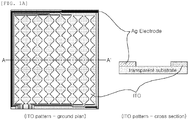
- the capacitive touch screen that is applied to Mobile, MP2 device, Note Book, and the like, generally uses ITO (Indume Tin Oxide) transparency electrode.
- Fig 1a is a cross-sectional view of a touch panel including ITO material according to the prior art
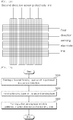
- Fig 1b and Fig. 1c are processes for manufacturing a touch panel including ITO material according to the prior art, which are flow charts of a photo etching process and a screen printing process, respectively.
- the touch screen using the capacitive way according to the prior art has poor touch sensitivity because sensing and motion sensors are formed by patterning ITO transparency electrode, so that it is not suitable for making a large area.
- an optical transmittance is not good and also visibility is bad due to the pattern of sensor electrode.
- the touch panel according to the prior art is manufactured by the photo etching process for forming a wiring and a pattern of ITO transparency electrode or a screen-printing process for forming a pattern of silver electrode.
- Patent KR10-2009-0015414 and US2002/0185981 disclose examples of these types of touch panel using pattern electrodes.
- the process is complex and the cost of manufacturing is high due to a photolithography process.
- the process is difficult to accurately control so that it is difficult to maintain an accurate align tolerance between ITO and outer electrode part; a line width is difficult to finely implement so that there are many dead spaces; a crack may be generated on the ITO micro line width part due to the high-temperature drying; and the cost of ITO material is high so that the cost for manufacturing the touch screen and touch pad including ITO material is high.
- An object of the present invention is to provide a capacitive touch panel and a method for manufacturing the same, in which the capacitive touch panel has an intaglio micro pattern formed by imprinting process and a conductive layer formed in the intaglio. with low resistance as compared with ITO, and various fill factors.
- Another object of the present invention is to provide a capacitive touch panel and a method for manufacturing the same, in which the capacitive touch panel is manufactured by forming a sensing electrode and a wiring electrode at the same time in the intaglio after processing the intaglio pattern on a resin layer laminated on a transparency substrate.
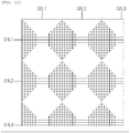
- Fig. 2a and Fig. 2b are plan views of a first sensing layer including a x-axis sensing electrode of an upper layer of a touch panel according to an embodiment of the present invention and of a second sensing layer including a y-axis sensing electrode of a lower layer of the touch panel, respectively.
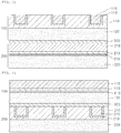
- Fig. 3 is a cross-sectional view along with a line A-A' of Fig. 2a and Fig. 4 is a cross-sectional view along with a line B-B' of Fig. 2a .
- Fig 5 shows a part of intaglio that is formed on a resin layer, in which the intaglio will be filled with sensing electrodes.
- the touch panel 10 is composed of a first sensing layer 100 including a plurality of first direction sensing electrodes 115 which are patterned and a plurality of first wiring electrodes 140, and a second sensing layer 200 including a plurality of second direction sensing electrodes 215 which are patterned and a plurality of second wiring electrodes 240.
- the plurality of the first wiring electrodes 140 and the plurality of the second wiring electrodes 240 are described in detail in Fig. 9 .
- the first sensing layer 100 and the second sensing layer 200 are formed by mutually bonding their broad sides in a vertical direction.
- One ends of the first direction sensing electrodes 115 are connected to the plurality of the first direction sensing electrodes lines D1L1, 2, 3..., and one ends of the second direction sensing electrodes 215 are connected to the plurality of the second direction sensing electrodes lines D2L1, 2, 3....
- the number of the plurality of the first and second directions sensing electrodes and the plurality of the first and second directions sensing electrodes lines may be determined widely and variously according to the uses of the touch panel.
- the first sensing layer 100 is the upper layer and the second sensing layer 200 is the lower layer. That is, the second sensing layer is firstly formed and the first sensing layer is formed on the second sensing layer.
- the material such as an adhesive, for example, OCA (Optical Clear Adhesive), and the like, which has an adhesive property, is included on the bottom part of the first sensing layer 100 without a separate bonding layer so that the first sensing layer is preferably bonded to the upper part of the second sensing layer 200.
- the bonding layer 300 in this situation is preferably Optical Clear Adhesive of a film type.
- the separate bonding layer 300 it is of great advantage in terms of insulating aspect.
- the touch panel may be formed by bonding any one of the sensing layers with the upper part or the bottom part of the other sensing layer after forming the first and second sensing layers at the same time.
- Each of the first direction sensing electrode 115 and the second direction sensing layer 215 is located on the first sensing layer 100 and the second sensing layer 200 to mutually cross in a space.
- the first direction sensing electrodes may be formed in a widthwise direction on the first sensing layer and the second direction sensing electrodes may be formed in a lengthwise direction on the second sensing layer.
- the first direction sensing electrodes are formed in a plurality of first regions R1 for sensing object's touch and a plurality of second regions R2 for connecting the first regions on the surface of the touch panel 10.
- the second direction sensing electrodes include a plurality of first regions R3 and a plurality of second regions R4, which have the same shape as the plurality of the first regions R1 and the plurality of the second regions R2, except in that the first regions R1 is formed in the lengthwise direction and the second regions R2 is formed in the widthwise direction on the first sensing layer.
- the first regions R1 of the first sensing layer sense positional information of a horizontal axis
- the first regions R3 of the second sensing layer performs the operation for sensing positional information of a vertical axis. Therefore, the touch point can be correctly found on the touch panel 10.
- the plurality of the first regions R1, R3 are preferably formed more broadly as compared with the plurality of the second regions R2, R4 for easily sensing the object that is touched on the surface of the touch panel.
- the plurality of the first regions R1, R3 and the plurality of the second regions R2, R4 may be formed to surround their edges by edge electrodes 115c.
- the plurality of the first regions R1 has various shapes, such as diamonds, hexagon, and the like, and sensing electrodes having a lattice shape form inside the regions. That is, as shown in Fig. 2a and Fig. 2b , a plurality of sensing electrodes 115a in a widthwise direction and a plurality of sensing electrode 115b in a lengthwise direction may be formed to cross mutually so that the first regions R1, R3 may be formed in a lattice shape.
- a crossing region 211c between an intaglio region 211a to be filled with widthwise direction electrodes and an intaglio region 211b to be filled with lengthwise direction electrodes among the electrodes composing the sensing electrodes is formed a little bit broadly than non-crossing regions 211a, 211b.
- the plurality of the first regions R1, R3 may not be overlapped mutually in a vertical direction of the first and second sensing layers and the plurality of the second regions R2, R4 may be overlapped in a vertical direction with the second region of the first sensing layer and the second region of the second sensing layer.
- each pattern of the second region R2 of the first sensing layer and the second region R4 of the second sensing layer may be formed in a different pattern from each pattern of the first region of the first sensing layer and the first region of the second sensing layer.
- the pattern formed by vertically overlapping the second region R2 of the first sensing layer and the second region R4 of the second sensing layer may preferably be formed to be the same or similar with the pattern of the first region of the first sensing layer or the pattern of the first region of the second sensing layer.
- An optical transmittance of the sensing layer can be improved by forming the sensing electrodes in a lattice shape of widthwise direction and lengthwise direction on the first sensing layer and the second sensing layer.
- the ends of the plurality of sensing electrodes 115b, 215a of lengthwise direction and the sensing electrodes 115a, 215d of widthwise direction are connected to edge electrodes 115c, 215c thereby preventing an increase of resistance capacity of the first regions R1, R3 so that a sufficient amount of current can be flowed into the first and second sensing electrodes of the first and second layers and then finally a touch sensitivity of the touch panel can be improved.
- the first region R1 of the first sensing layer 100 and the first region R3 of the second sensing layer 200 are arranged to not overlap mutually in a vertical direction of the first and second sensing layers. Looking the touch panel 10 down from the first sensing layer 100 that is the upper layer, the first region R1 of the first sensing layer 100 is projected onto the region 110 on which any sensing electrode on the second sensing layer 200 is not formed.
- the resin layers 110, 210 including the patterned layers on the transparent substrate 120 are laminated on the first sensing layer 100 and the second sensing layer 200 and an intaglio is formed inside thereof.
- the intaglio includes the seed layers 113, 213 and a metal layer for forming the sensing electrodes 115, 215 and the wiring electrodes 140, 240 inside thereof.
- the intaglio according to the present embodiment does not penetrate to the transparent substrate because the resin layers 110, 210 are still remained in the bottom part.
- the first sensing layer 100 and the second sensing layer 200 are bonded by the bonding layer 300.
- the patterned layer means the region formed with the intaglio on the resin layer according to the pattern of the sensing electrodes.
- Fig. 6 shows cross-sectional shapes of intaglio that are formed by molds having various shapes and relevant molds that are used for forming the intaglio on the patterned layer
- Fig. 7 is a plan view of the patterned layer on the intaglio that is formed by a mold having a square shape.
- the cross-section of the intaglio to be formed with the sensing electrodes on the resin layer 110 laminated on the transparent substrate 120 and the mold 400 forming the intaglio are shown.
- the cross-section of the intaglio may be a square, a triangle, and a diamond shapes.
- the width of the intaglio and the pitch that is an interval between the intaglios for forming a lattice pattern should have the value within a certain range as disclosed in Table 1 so that Fill Factor can be obtained.
- the depth of the intaglio may be formed to have the same height with the height of the resin layer to be formed, but a part of resin layer is still remained on the floor surface of the intaglio so that the surface of the transparent substrate and the metal layer should not preferably be contacted.
- the Fill Factor as defined above is less than 1.4, the optical transmittance is increased but the touch motion is possible to not smoothly perform due to the decrease of the contact area for capacitance and the increase of resistance of the conductive layer; and when the fill factor is above 10, there are disadvantages such that the pattern of the sensing electrodes is sighted and the transmittance is decreased due to the increase of the area of the conductive layer.
- the Fill Factor preferably has the value between 1.4 ⁇ 7.0 %, and the line width of the sensing electrodes and the pitch are preferably used by adjusting properly according to the value of the Fill Factor.
- Line Width Pitch Fill ( ⁇ m) ( ⁇ m) Factor (%) 1 ⁇ 5 100 1.9 ⁇ 10 200 2.5 ⁇ 5.0 300 1.9 ⁇ 3.5 400 1.4 ⁇ 2.5 500 0.4 ⁇ 1.9 600 0.3 ⁇ 1.7 6 ⁇ 10 100 11 ⁇ 19 200 5.9 ⁇ 10 300 3.9 ⁇ 7.0 400 2.9 ⁇ 5.0 500 2.3 ⁇ 3.9 600 1.9 ⁇ 3.3
- Fig. 8a to Fig. 8f show a process for forming sensing electrodes when the cross-section of the intaglio is a square in any sensing layer of a touch panel according an embodiment of the present invention
- Fig. 9 shows the sensing electrodes and the wiring electrodes together that are formed on the edge of the sensing layer
- Fig. 10 shows a process for removing the metallic material and the conductive polymer remained on the surface of the patterned layer except the sensing electrodes after coating the metallic material or the conductive polymer without the seed layer in the intaglio.
- Fig. 13 is a flow chart of method for manufacturing a touch panel according to an embodiment of the present invention
- Fig. 14 is a flow chart of a process for forming the sensing layer of Fig. 13 .
- the touch panel that is composed of the sensing layers is produced by the method comprising: forming the second sensing layer having the second sensing electrodes that are patterned in a second direction (S100); forming the bonding layer that is an adhesive (OCA) for bonding the first sensing layer on the surface of the second sensing layer (S200); and forming the first sensing layer having the first sensing electrodes that are patterned in a first direction on the surface of the bonding layer.
- S100 second direction
- OCA adhesive
- the adhesive is a film type, and preferably allows to bond the first and second sensing layers by laminating between the first sensing layer and the second sensing layer.
- the first sensing layer and the second sensing layer may be mutually bonded by including an adhesion material on the lower side of the upper layer. That is, any one sensing layer from the first and second sensing layers includes the material having an adhesion on the lower part thereof thereby having a role as the bonding layer without a separate bonding layer so that the thickness of the touch panel can be decreased.
- the first sensing layer and the second sensing layer are formed through the same process. Referring to Fig. 8a to Fig. 8f , the process for forming the sensing layer will be described in detail based on the second sensing layer.
- the resin layer 210 is laminated on the transparent substrate 220 (S110, S310).
- the resin film or glass can be used as the transparent substrate 220.
- thermoplastic resin such as polyethyleneterephthalate (PET), polycarbonate (PC), polymethylmetharylate (PMMA), triacetate cellulose (TAC), polyethersulfone (PES), and the like
- PET polyethyleneterephthalate
- PC polycarbonate
- PMMA polymethylmetharylate
- TAC triacetate cellulose
- PES polyethersulfone
- the material including an adhesive such as PSA (Pressure Sensitive Adhesive) can be used.
- UV curing resin or thermo-setting resin can be used as the resin layer 210.
- the intaglio 211 is formed by imprinting the mold 400 on the resin layer 210.
- the intaglio 211 is formed according to the pattern to be formed with the plurality of the first and second direction sensing electrodes and the plurality of the first and second wiring electrodes (S120, S320).
- the intaglio 211 may be formed by curing the resin layer 210 through giving UV or heat in a state of pressing the mold 400 on the resin material before curing the resin material, and then removing the mold 400 after curing the resin material.
- an embossed mold 300 is used for forming the intaglio on the resin layer 210, and is preferably the material having a quality of a sufficiently lower surface roughness. After pattering the intaglio according to the mold, it is preferable to have Haze of less than 4 %.
- a pattern type of the intaglio formed on the resin layer 210 according to the present embodiment is a square, but the cross-sectional shapes of the intaglio having various patterns can be obtained by using the molds having various shapes as shown in Fig. 6 .
- the pattern size of the intaglio formed on the resin layer 210 can be different according to the embodiments, but it preferably is that the line width of the electrode is 1 ⁇ m ⁇ 10 ⁇ m, the depth of the electrode is 1 ⁇ m ⁇ 10 ⁇ m, and the pitch between of the electrodes is 200 ⁇ m ⁇ 600 ⁇ m.
- the internal surface of the intaglio 211 and the surface of the resin layer 210 are preferably surface-treated in order to improve an adhesive property between the resin layer 210 and the seed layer 213 to be formed in the subsequent process, and the part that is surface-treated may be marked as the surface-treated layer 212 as shown in Fig. 8c (S130, S330).
- a method for surface-treating may include a chemical etching using alkali-based aqueous solution or catalyst treatments, and plasma or ion beam treatments, and the like.
- the metallic seed layer 213 is formed on the surface-treated layer 212 (S140, S340).
- the seed layer 213 may be formed by using an electroless plating, CVD deposition, sputtering or printing using a metal material.
- the material for the seed layer may include any one of copper (Cu), nickel (Ni), chromium (Cr), iron (Fe), tungsten (W), phosphorus (P), cobalt (Co), silver (Ag), silver-carbon (Ag-C), nickel-phosphorus (Ni-P), copper oxide II (CuO), and inorganic matter (SiO 2 ), or alloy thereof; and its thickness preferably is 0.01 ⁇ m ⁇ 5 ⁇ m.
- the process for removing the seed layer 213 from the surface of the resin layer other than the patterned region of the intaglio includes selectively removing (S160, S360) the resin that is filled inside the intaglio and the seed layer formed on the surface of the resin layer by depositing in an etching solution after filling (S150, S350) with the resin having an etch resistance inside the intaglio that is the patterned region.
- a chemical used for the etching includes any one of a type of nitric acid, a type of sulfuric acid, a type of hydrochloric acid, a type of copper sulphate, ferric chloride, and copper shloride.
- the sensing electrodes 215 and the wiring electrodes 240 may be formed by an electroless plating, an electro plating, CVD deposition, sputtering, coating or printing on the seed layer 213 (S170, S370).
- the sensing electrodes and the wiring electrodes are formed at the same time, and preferably by using the material having a lower resistance than ITO (Indume Tin Oxide).
- ITO Indume Tin Oxide
- any one of copper (Cu), silver (Ag), silver-carbon (Ag-C), aluminum (Al), nickel (Ni), chromium (Cr), and nickel-phosphorus (Ni-P), or alloy thereof can be used as the raw material for the sensing electrode 215 and the wiring electrode 240.
- each of the first and second wiring electrodes 140, 240 may be formed at the same time with each of the first and second direction sensing electrodes on the part of edge of each of the first and second sensing layers in a broader width than the width of each of the first and second direction sensing electrodes.
- the sensing layer may be formed by wiping or scratching with a blade 230 on the surface to be free of residue after coating the metallic material or conductive polymer without the metallic seed layer on the patterned layer (S180, S380).
- the conductive polymer coated on the surface of the patterned layer has a thickness of 1 ⁇ m-10 ⁇ m.
- the height of the metal layer filled on the intaglio pattern of the resin layer 210 is preferably the same or lower than the depth of the intaglio pattern formed on the resin layer 210.
- the pattern of the sensing electrodes of the touch panel is only an embodiment, but a plurality of the sensing electrodes that perform the functions of sensing and operating of the touch may be patterned in various structures and then applied.
- the pattern of the sensing electrode as mentioned above relates to the Fill Factor that is calculated as a ratio of the area the patterned layer formed with the sensing electrodes to the area of the sensing electrodes, and the Fill Factor of the touch panel according to the present embodiment is disclosed in Table 1.
- Fig. 11 is a plan view of any sensing layer having the sensing electrodes that are formed on the touch panel according to another embodiment of the present invention
- Fig. 12 is a plan view of sensing electrodes that are formed on the touch panel according another embodiment of the present invention.
- Fig. 11 is an embodiment applied with the structure of a minimized sight clearance by removing the edge electrode formed outside of the sensing and operating regions of the sensing electrodes of Fig. 2a and Fig. 2b , and even in this situation, the Fill Factor in the cross region between the widthwise sensing electrode and the lengthwide sensing electrode formed on the same sensing layer is the same with Table 1.
- Fig. 12 shows a plurality of fine sensing elecrodes in a vertical or horizontal direction on each sensing layer, and the sensing electrodes on the different sensing layer each other on the plan view of the touch panel are displayed in a lattice shape that are intersected in X and Y axis.
- the Fill Factor on the part in which the sensing electrode lines are intersected in X and Y-axis is the same with Table 1.
- the above structure has an advantage structure in terms of the sight clearance of the sensing electrodes as compared with the shape of the sensing electrodes having the edge electrodes as disclosed in Fig. 2a and Fig. 2b .
- the sensing electrode may have various Fill Factors for the line width and pitch of the sensing electordes, and also the sensing electrodes can be composed in various shapes of their section, such as a square, a pentagon, a hexagon, an oval, and the like.
- the capacitive touch panel and method for manufacturing the same can provide the touch panel having various Fill Factors that are formed with the conductive layer having a low resistance as compared with ITO on the intaglio after a fine pattern of the intaglio applied with the imprinting process, thereby improving the touch sensitivity and performance and also making a large area.
- the capacitive touch panel and method for manufacturing the same according to the present embodiment can improve the optical transmittance that can be limited due to the sensing electrode and also the sight clearance by arranging the sensing electrode in a lattice shape.
- the capacitive touch panel and method for manufacturing the same according to the present embodiment can provide an excellent durability by preventing an exposure of the electrode part by forming the electrode part on the intaglio.
- the capacitive touch panel and method for manufacturing the same can reduce the time and the process for manufacturing, and also increase productivity and reduce the cost for manufacturing by forming the sensing electrode and the wiring electrode at the same time on the intaglio of the fine pattern formed on the resin layer.
Landscapes
- Engineering & Computer Science (AREA)
- General Engineering & Computer Science (AREA)
- Theoretical Computer Science (AREA)
- Human Computer Interaction (AREA)
- Physics & Mathematics (AREA)
- General Physics & Mathematics (AREA)
- Position Input By Displaying (AREA)
Applications Claiming Priority (3)
| Application Number | Priority Date | Filing Date | Title |
|---|---|---|---|
| KR1020100019102A KR20110100034A (ko) | 2010-03-03 | 2010-03-03 | 정전 용량 방식 터치 패널 및 그 제조방법 |
| KR1020100076269A KR101728818B1 (ko) | 2010-08-09 | 2010-08-09 | 정전용량 방식의 터치 패널 및 그 제조 방법 |
| PCT/KR2011/001478 WO2011108869A2 (ko) | 2010-03-03 | 2011-03-03 | 정전 용량 방식 터치 패널 및 그 제조방법 |
Publications (3)
| Publication Number | Publication Date |
|---|---|
| EP2544080A2 EP2544080A2 (en) | 2013-01-09 |
| EP2544080A4 EP2544080A4 (en) | 2016-05-18 |
| EP2544080B1 true EP2544080B1 (en) | 2019-08-28 |
Family
ID=44542728
Family Applications (1)
| Application Number | Title | Priority Date | Filing Date |
|---|---|---|---|
| EP11750926.5A Active EP2544080B1 (en) | 2010-03-03 | 2011-03-03 | Capacitive touch panel and manufacturing method for same |
Country Status (6)
| Country | Link |
|---|---|
| US (1) | US9244573B2 (https=) |
| EP (1) | EP2544080B1 (https=) |
| JP (1) | JP2013521563A (https=) |
| CN (1) | CN102782624B (https=) |
| TW (1) | TWI461996B (https=) |
| WO (1) | WO2011108869A2 (https=) |
Families Citing this family (112)
| Publication number | Priority date | Publication date | Assignee | Title |
|---|---|---|---|---|
| TWI567912B (zh) * | 2011-02-18 | 2017-01-21 | 富士軟片股份有限公司 | 導電片以及觸控面板 |
| KR101303635B1 (ko) * | 2011-05-26 | 2013-09-11 | 엘지이노텍 주식회사 | 터치윈도우 |
| KR101978666B1 (ko) * | 2011-06-10 | 2019-05-15 | 미래나노텍(주) | 터치 스크린 센서 기판, 터치 스크린 센서 및 이를 포함하는 패널 |
| KR101330757B1 (ko) * | 2011-07-28 | 2013-11-18 | 엘지이노텍 주식회사 | 터치윈도우 및 이를 포함하는 액정표시장치 |
| JP5506758B2 (ja) * | 2011-10-03 | 2014-05-28 | 三菱電機株式会社 | タッチスクリーン、タッチパネル及びそれを備える表示装置 |
| TW201337705A (zh) * | 2011-10-25 | 2013-09-16 | Unipixel Displays Inc | 偏光膜電阻式觸控螢幕 |
| GB2510294A (en) * | 2011-10-25 | 2014-07-30 | Unipixel Displays Inc | Method of manufacturing a resistive touch sensor circuit by flexographic printing |
| KR101611379B1 (ko) * | 2011-10-25 | 2016-04-12 | 유니-픽셀 디스플레이스, 인코포레이티드 | 편광판 정전용량 방식 터치 스크린 |
| KR101373044B1 (ko) | 2012-04-19 | 2014-03-11 | 삼성디스플레이 주식회사 | 터치 스크린 패널 |
| KR20130118082A (ko) * | 2012-04-19 | 2013-10-29 | 삼성전기주식회사 | 터치패널 및 그 제조방법 |
| KR20130119045A (ko) * | 2012-04-23 | 2013-10-31 | 삼성전자주식회사 | 터치 패널 및 그의 제조 방법 |
| EP2662758A3 (en) | 2012-05-09 | 2015-03-04 | LG Innotek Co., Ltd. | Electrode member and touch window including the same |
| CN102722279A (zh) * | 2012-05-09 | 2012-10-10 | 崔铮 | 金属网格导电层及其具备该导电层的触摸面板 |
| KR20130127848A (ko) * | 2012-05-15 | 2013-11-25 | 삼성전기주식회사 | 터치센서 및 그 제조방법 |
| KR20140030727A (ko) * | 2012-09-03 | 2014-03-12 | 삼성전기주식회사 | 터치패널 및 그 제조방법 |
| CN103809796B (zh) * | 2012-11-09 | 2018-03-16 | 宝宸(厦门)光学科技有限公司 | 触控感应电极结构及其制造方法 |
| JP5559857B2 (ja) * | 2012-11-14 | 2014-07-23 | ホシデン株式会社 | タッチセンサ及びタッチセンサの製造方法 |
| CN103853380B (zh) * | 2012-12-03 | 2017-04-12 | Lg伊诺特有限公司 | 电极构件及包括该电极构件的触屏 |
| KR101555015B1 (ko) * | 2012-12-28 | 2015-09-22 | 주식회사 잉크테크 | 전도성 패턴의 형성방법 |
| CN103106953B (zh) * | 2013-02-06 | 2014-11-26 | 南昌欧菲光科技有限公司 | 导电膜及其制备方法以及包含该导电膜的触摸屏 |
| CN103187119B (zh) * | 2013-02-06 | 2014-08-06 | 南昌欧菲光科技有限公司 | 导电膜及其制备方法以及包含该导电膜的触摸屏 |
| US9217678B2 (en) * | 2013-02-06 | 2015-12-22 | Nanchang O-Film Tech Co., Ltd. | Touch sensor panel with conductive wires and color traces |
| US8828503B1 (en) * | 2013-02-28 | 2014-09-09 | Eastman Kodak Company | Making multi-layer micro-wire structure |
| KR101568079B1 (ko) | 2013-03-07 | 2015-11-10 | 주식회사 엘지화학 | 금속 세선을 포함하는 투명 기판 및 그 제조 방법 |
| US9164595B2 (en) * | 2013-03-08 | 2015-10-20 | Darren C. PETERSEN | Mechanical actuator apparatus for a touchscreen |
| US9158390B2 (en) | 2013-03-08 | 2015-10-13 | Darren C. PETERSEN | Mechanical actuator apparatus for a touch sensing surface of an electronic device |
| CN103176656B (zh) * | 2013-03-20 | 2015-05-13 | 南昌欧菲光科技有限公司 | 触摸屏及其制造方法 |
| CN103345317B (zh) * | 2013-03-25 | 2014-10-29 | 深圳欧菲光科技股份有限公司 | 触摸屏 |
| US20140293149A1 (en) * | 2013-03-27 | 2014-10-02 | Shenzhen O-Film Tech Co., Ltd | Capacitive touch screen and manufacturing method thereof |
| JP6056594B2 (ja) * | 2013-03-27 | 2017-01-11 | 大日本印刷株式会社 | タッチパネルセンサ部材の製造方法 |
| CN103165226B (zh) * | 2013-03-28 | 2015-04-08 | 南昌欧菲光科技有限公司 | 透明导电膜及其制备方法 |
| US9392700B2 (en) | 2013-03-28 | 2016-07-12 | Nanchang O-Film Tech. Co., Ltd. | Transparent conductive film and preparation method thereof |
| US9089061B2 (en) * | 2013-03-30 | 2015-07-21 | Shenzhen O-Film Tech Co., Ltd. | Conductive film, method for making the same, and touch screen including the same |
| US9639215B2 (en) * | 2013-03-30 | 2017-05-02 | Shenzhen O-Film Tech Co., Ltd. | Touch screen |
| CN103164082B (zh) * | 2013-03-30 | 2015-07-08 | 深圳欧菲光科技股份有限公司 | 触摸屏 |
| CN103425325B (zh) * | 2013-03-30 | 2016-12-28 | 南昌欧菲光显示技术有限公司 | 偏光片模块及其制备方法和触摸显示屏 |
| US9538654B2 (en) * | 2013-03-30 | 2017-01-03 | Shenzhen O-Film Tech Co., Ltd. | Conductive film, method for manufacturing the same, and touch screen including the same |
| US20140293150A1 (en) * | 2013-04-02 | 2014-10-02 | Shenzhen O-Film Tech Co., Ltd | Touch screen |
| US20140307178A1 (en) * | 2013-04-12 | 2014-10-16 | Shenzhen O-Film Tech Co., Ltd | Touch screen sensing module, manufacturing method thereof and display device |
| CN103235660B (zh) * | 2013-04-12 | 2014-08-06 | 深圳欧菲光科技股份有限公司 | 双层触摸屏及其制备方法 |
| CN103218081B (zh) * | 2013-04-12 | 2014-08-06 | 深圳欧菲光科技股份有限公司 | 双层触摸屏及其制备方法 |
| KR101688986B1 (ko) * | 2013-04-19 | 2016-12-23 | 주식회사 잉크테크 | 디스플레이용 투명전극 필름 제조방법 및 디스플레이용 투명전극 필름 |
| CN105378856B (zh) * | 2013-05-16 | 2019-07-12 | 印可得株式会社 | 透明电极薄膜的制造方法 |
| KR20140137304A (ko) * | 2013-05-22 | 2014-12-02 | 미래나노텍(주) | 정전용량 방식의 터치 패널 및 터치 스크린 |
| CN103345961A (zh) * | 2013-05-30 | 2013-10-09 | 南昌欧菲光科技有限公司 | 透明导电膜 |
| CN103294272B (zh) * | 2013-05-30 | 2016-04-13 | 南昌欧菲光科技有限公司 | 透明导电膜 |
| CN103295671B (zh) | 2013-05-30 | 2016-08-10 | 南昌欧菲光科技有限公司 | 透明导电膜 |
| CN103279240B (zh) * | 2013-05-30 | 2016-03-09 | 南昌欧菲光科技有限公司 | 触控面板 |
| CN103295670B (zh) * | 2013-05-30 | 2015-11-25 | 南昌欧菲光科技有限公司 | 透明导电膜 |
| KR20150006681A (ko) * | 2013-07-09 | 2015-01-19 | 삼성전기주식회사 | 원격제스처 인식이 가능한 터치스크린 및 이의 제어방법 |
| KR102108846B1 (ko) * | 2013-07-16 | 2020-05-11 | 엘지이노텍 주식회사 | 터치 윈도우 |
| TW201514802A (zh) * | 2013-07-16 | 2015-04-16 | Lg Innotek Co Ltd | 觸控螢幕以及包含其之觸控裝置 |
| KR20150009846A (ko) * | 2013-07-17 | 2015-01-27 | 삼성디스플레이 주식회사 | 터치 스크린 패널 및 그 제조 방법 |
| KR102107107B1 (ko) * | 2013-07-25 | 2020-05-07 | 삼성디스플레이 주식회사 | 터치 스크린 패널, 터치 스크린 패널 일체형 평판 표시 장치 및 이의 제조 방법 |
| JP5560364B1 (ja) * | 2013-07-26 | 2014-07-23 | 株式会社フジクラ | 導体パターン付き基板及びタッチパネル |
| CN103425339B (zh) * | 2013-07-30 | 2017-03-22 | 南昌欧菲光科技有限公司 | 单层多点式触控导电膜及单层多点式触控屏 |
| CN103425341B (zh) * | 2013-07-30 | 2016-10-26 | 南昌欧菲光科技有限公司 | 单层多点式触控屏及其单层多点式导电膜 |
| CN103426504B (zh) * | 2013-07-30 | 2017-04-05 | 南昌欧菲光科技有限公司 | 导电膜 |
| CN103425343B (zh) * | 2013-07-30 | 2016-09-21 | 南昌欧菲光科技有限公司 | 单层多点式触控导电膜及单层多点式触控屏 |
| CN103426503A (zh) * | 2013-07-30 | 2013-12-04 | 南昌欧菲光科技有限公司 | 单层多点式触控屏及其单层多点式导电膜 |
| CN103425340B (zh) * | 2013-07-30 | 2017-11-21 | 南昌欧菲光科技有限公司 | 单层多点式触控屏及其单层多点式导电膜 |
| CN103455198B (zh) * | 2013-07-30 | 2016-12-28 | 南昌欧菲光科技有限公司 | 单层多点式触控屏及其单层多点式导电膜 |
| CN103425342B (zh) * | 2013-07-30 | 2016-09-21 | 南昌欧菲光科技有限公司 | 单层多点式触控导电膜及单层多点式触控屏 |
| CN104345938A (zh) * | 2013-07-31 | 2015-02-11 | 南昌欧菲光科技有限公司 | 一种透明导电膜及其引线电极 |
| CN104345939A (zh) * | 2013-07-31 | 2015-02-11 | 南昌欧菲光科技有限公司 | 一种透明导电膜及其引线电极 |
| CN104347154B (zh) * | 2013-07-31 | 2017-11-03 | 南昌欧菲光科技有限公司 | 一种透明导电膜 |
| CN103425346A (zh) * | 2013-07-31 | 2013-12-04 | 南昌欧菲光科技有限公司 | 柔性触摸装置 |
| JP6339780B2 (ja) * | 2013-08-27 | 2018-06-06 | エルジー イノテック カンパニー リミテッド | タッチパネル及びディスプレイ |
| KR102142855B1 (ko) * | 2013-08-29 | 2020-08-31 | 미래나노텍(주) | 터치스크린 패널용 배선 전극, 이를 이용한 터치스크린 패널 및 그 제조방법 |
| KR102130592B1 (ko) * | 2013-09-09 | 2020-07-06 | 엘지전자 주식회사 | 터치 패널, 그리고 터치 패널용 도전층의 제조 방법 |
| US9155201B2 (en) | 2013-12-03 | 2015-10-06 | Eastman Kodak Company | Preparation of articles with conductive micro-wire pattern |
| US9699898B2 (en) | 2013-12-27 | 2017-07-04 | Lg Chem, Ltd. | Conductive film and method for manufacturing same |
| DE102014100246A1 (de) * | 2014-01-10 | 2015-07-16 | Polyic Gmbh & Co. Kg | Kapazitives Sensorelement sowie Verfahren zur Herstellung dazu |
| CN104793772A (zh) * | 2014-01-17 | 2015-07-22 | 湖北华尚光电有限公司 | 触摸显示屏、触摸感应盖板及其制造方法 |
| JP6256033B2 (ja) * | 2014-01-20 | 2018-01-10 | 大日本印刷株式会社 | タッチパネルセンサ、タッチパネルセンサの製造方法およびタッチ位置検出機能付き表示装置 |
| US9857906B2 (en) * | 2014-01-22 | 2018-01-02 | Lg Innotek Co., Ltd. | Touch window |
| CN104978059A (zh) * | 2014-04-14 | 2015-10-14 | 冠捷投资有限公司 | 触控模块的制造方法与其触控模块 |
| CN105094395A (zh) * | 2014-05-04 | 2015-11-25 | 宸鸿科技(厦门)有限公司 | 触控装置 |
| CN105084303A (zh) * | 2014-05-21 | 2015-11-25 | 上海蓝沛新材料科技股份有限公司 | 一种微纳铜线结构及其制备方法 |
| CN105101655B (zh) * | 2014-05-23 | 2018-11-30 | 上海量子绘景电子股份有限公司 | 在特种产品基材表面制备微纳米级别金属电极的方法 |
| US10537028B2 (en) | 2014-06-30 | 2020-01-14 | 3M Innovative Properties Company | Metallic microstructures with reduced-visibility and methods for producing same |
| EP2966549B1 (en) * | 2014-07-11 | 2021-10-06 | LG Innotek Co., Ltd. | Electrode member and touch window including the same |
| US20170177114A1 (en) * | 2014-08-07 | 2017-06-22 | 3M Innovative Properties Company | Force-sensing capacitor elements, deformable membranes and electronic devices fabricated therefrom |
| TWI556698B (zh) * | 2014-08-12 | 2016-11-01 | 旭德科技股份有限公司 | 基板結構及其製作方法 |
| EP2985680B1 (en) | 2014-08-14 | 2017-05-17 | LG Electronics Inc. | Conductive film, touch panel including the conductive film and display apparatus including the conductive film |
| KR102209305B1 (ko) * | 2014-08-14 | 2021-01-29 | 엘지전자 주식회사 | 전도성 필름, 그리고 이를 포함하는 터치 패널 및 디스플레이 장치 |
| CN105589586B (zh) * | 2014-10-21 | 2019-06-14 | 宸鸿光电科技股份有限公司 | 触控面板 |
| WO2016098268A1 (ja) * | 2014-12-18 | 2016-06-23 | 凸版印刷株式会社 | 電極付きカラーフィルタ基板、該基板を含む表示装置、ならびに該基板の製造方法 |
| KR101636064B1 (ko) * | 2015-02-23 | 2016-07-06 | (주)뉴옵틱스 | 터치패널용 센서시트 |
| CN104777653B (zh) * | 2015-05-08 | 2017-12-12 | 厦门天马微电子有限公司 | 阵列基板、液晶显示面板和液晶显示装置 |
| CN105093606B (zh) * | 2015-05-08 | 2018-03-27 | 厦门天马微电子有限公司 | 阵列基板、液晶显示面板和液晶显示装置 |
| CN105335006A (zh) * | 2015-11-18 | 2016-02-17 | 业成光电(深圳)有限公司 | 触控面板 |
| KR101728329B1 (ko) * | 2015-11-19 | 2017-05-02 | 현대자동차주식회사 | 터치 입력장치, 이를 포함하는 차량, 및 그 제조방법 |
| CN107124900A (zh) * | 2015-12-25 | 2017-09-01 | 松下知识产权经营株式会社 | 触摸面板和使用该触摸面板的显示装置 |
| WO2018087631A1 (en) | 2016-11-09 | 2018-05-17 | Semiconductor Energy Laboratory Co., Ltd. | Display device, display module, electronic device, and method for manufacturing the display device |
| KR102720533B1 (ko) | 2016-12-05 | 2024-10-24 | 삼성디스플레이 주식회사 | 터치 센서 및 이를 구비한 디스플레이 장치 |
| KR102811755B1 (ko) | 2017-02-03 | 2025-05-23 | 삼성디스플레이 주식회사 | 터치 센서 및 이를 구비한 디스플레이 장치 |
| CN108573997B (zh) | 2017-03-14 | 2023-12-01 | 三星显示有限公司 | 显示装置 |
| KR102355519B1 (ko) | 2017-05-02 | 2022-01-26 | 삼성디스플레이 주식회사 | 터치 센서 및 그의 구동 방법 |
| KR101932650B1 (ko) | 2017-05-15 | 2018-12-28 | 삼성디스플레이 주식회사 | 터치 센서 및 이를 구비한 디스플레이 장치 |
| KR102375273B1 (ko) | 2017-05-15 | 2022-03-18 | 삼성디스플레이 주식회사 | 터치 센서 및 그의 구동 방법 |
| KR20190006835A (ko) * | 2017-07-11 | 2019-01-21 | 엘지디스플레이 주식회사 | 유기발광소자를 이용한 조명장치 및 그 제조방법 |
| JP7172211B2 (ja) | 2017-07-28 | 2022-11-16 | Tdk株式会社 | 導電性基板、電子装置及び表示装置 |
| JP7375294B2 (ja) * | 2017-07-28 | 2023-11-08 | Tdk株式会社 | 導電性基板、電子装置及び表示装置の製造方法 |
| KR102410267B1 (ko) | 2017-09-08 | 2022-06-20 | 삼성디스플레이 주식회사 | 입력 감지 유닛 및 이를 포함하는 전자 장치 |
| KR102456701B1 (ko) | 2017-09-29 | 2022-10-21 | 삼성디스플레이 주식회사 | 터치 센서 및 이를 구비한 디스플레이 장치 |
| US10353498B2 (en) * | 2017-12-08 | 2019-07-16 | Wuhan China Star Optoelectronics Semiconductor Display Technology Co., Ltd. | Touch structure for touch display panel |
| KR102508964B1 (ko) | 2018-01-31 | 2023-03-14 | 삼성디스플레이 주식회사 | 표시 장치 |
| WO2020056463A1 (en) * | 2018-09-19 | 2020-03-26 | Swinburne University Of Technology | Sensor array and sensor array system |
| KR20210070110A (ko) * | 2019-12-04 | 2021-06-14 | 주성엔지니어링(주) | 전극 형성 방법 |
| WO2021131319A1 (ja) * | 2019-12-25 | 2021-07-01 | パナソニックIpマネジメント株式会社 | タッチセンサ |
| CN113970985B (zh) * | 2021-11-05 | 2025-06-13 | 上海天马微电子有限公司 | 触控显示面板和显示装置 |
Citations (1)
| Publication number | Priority date | Publication date | Assignee | Title |
|---|---|---|---|---|
| KR20090095930A (ko) * | 2008-03-06 | 2009-09-10 | 미래나노텍(주) | 전자파 차폐 필름, 그것을 이용한 전면 필터 및 그 제조방법 |
Family Cites Families (23)
| Publication number | Priority date | Publication date | Assignee | Title |
|---|---|---|---|---|
| JP3935596B2 (ja) | 1998-03-13 | 2007-06-27 | 大日本印刷株式会社 | 電磁波遮蔽板の製造方法および電磁波遮蔽板 |
| US6498590B1 (en) * | 2001-05-24 | 2002-12-24 | Mitsubishi Electric Research Laboratories, Inc. | Multi-user touch surface |
| US6587750B2 (en) * | 2001-09-25 | 2003-07-01 | Intuitive Surgical, Inc. | Removable infinite roll master grip handle and touch sensor for robotic surgery |
| US7242393B2 (en) * | 2001-11-20 | 2007-07-10 | Touchsensor Technologies Llc | Touch sensor with integrated decoration |
| KR100604819B1 (ko) | 2003-06-12 | 2006-07-28 | 삼성전자주식회사 | 반도체 패키지용 배선 기판, 그 제조방법 및 이를 이용한반도체 패키지 |
| CN1324448C (zh) * | 2004-07-29 | 2007-07-04 | 义隆电子股份有限公司 | 使用薄膜的电容式触控板及其制作方法 |
| US8166649B2 (en) * | 2005-12-12 | 2012-05-01 | Nupix, LLC | Method of forming an electroded sheet |
| JP4664843B2 (ja) | 2006-03-22 | 2011-04-06 | 株式会社ワコム | 位置検出装置、センサパネル、および、表示装置 |
| JP5235315B2 (ja) | 2007-03-05 | 2013-07-10 | 株式会社カネカ | 透明電極付き基板の製造方法 |
| KR20090015414A (ko) * | 2007-08-08 | 2009-02-12 | 에이디반도체(주) | 정전용량 터치감지패널 |
| TWI378378B (en) * | 2008-03-19 | 2012-12-01 | Egalax Empia Technology Inc | Device and method for preventing the influence of conducting material from point detection of projected capacitive touch panel |
| WO2009108758A2 (en) * | 2008-02-28 | 2009-09-03 | 3M Innovative Properties Company | Touch screen sensor with low visibility conductors |
| KR101080183B1 (ko) | 2008-04-04 | 2011-11-07 | (주)멜파스 | 가장자리 위치 인식 특성이 개선된 접촉 감지 장치 |
| US8629842B2 (en) | 2008-07-11 | 2014-01-14 | Samsung Display Co., Ltd. | Organic light emitting display device |
| US9128568B2 (en) * | 2008-07-30 | 2015-09-08 | New Vision Display (Shenzhen) Co., Limited | Capacitive touch panel with FPC connector electrically coupled to conductive traces of face-to-face ITO pattern structure in single plane |
| JP5174575B2 (ja) * | 2008-07-31 | 2013-04-03 | グンゼ株式会社 | タッチパネル |
| CN104635983B (zh) * | 2008-07-31 | 2018-01-30 | 郡是株式会社 | 触摸开关 |
| US20100045625A1 (en) * | 2008-08-21 | 2010-02-25 | Tpo Displays Corp. | Touch panel and system for displaying images utilizing the same |
| TWI381302B (zh) * | 2008-11-12 | 2013-01-01 | Tpo Displays Corp | 影像顯示系統、電容觸控面板及其電容量測裝置與方法 |
| KR20090019881A (ko) | 2009-01-16 | 2009-02-25 | (주)유비엠디 | 정전용량방식의 터치 패널 및 이를 포함하는 키패드 일체형통신단말장치 |
| KR101577952B1 (ko) * | 2009-03-10 | 2015-12-17 | 삼성디스플레이 주식회사 | 터치 패널 장치 |
| JP2010271796A (ja) * | 2009-05-19 | 2010-12-02 | Optrex Corp | 電極間接続構造およびタッチパネル |
| JP5361579B2 (ja) | 2009-07-09 | 2013-12-04 | 信越ポリマー株式会社 | 大型ディスプレイ用のセンサパネル及びその製造方法 |
-
2011
- 2011-03-03 TW TW100107091A patent/TWI461996B/zh active
- 2011-03-03 CN CN201180011843.6A patent/CN102782624B/zh active Active
- 2011-03-03 US US13/582,410 patent/US9244573B2/en active Active
- 2011-03-03 EP EP11750926.5A patent/EP2544080B1/en active Active
- 2011-03-03 JP JP2012556019A patent/JP2013521563A/ja active Pending
- 2011-03-03 WO PCT/KR2011/001478 patent/WO2011108869A2/ko not_active Ceased
Patent Citations (1)
| Publication number | Priority date | Publication date | Assignee | Title |
|---|---|---|---|---|
| KR20090095930A (ko) * | 2008-03-06 | 2009-09-10 | 미래나노텍(주) | 전자파 차폐 필름, 그것을 이용한 전면 필터 및 그 제조방법 |
Also Published As
| Publication number | Publication date |
|---|---|
| EP2544080A2 (en) | 2013-01-09 |
| EP2544080A4 (en) | 2016-05-18 |
| JP2013521563A (ja) | 2013-06-10 |
| TW201203064A (en) | 2012-01-16 |
| CN102782624A (zh) | 2012-11-14 |
| US20120327021A1 (en) | 2012-12-27 |
| TWI461996B (zh) | 2014-11-21 |
| US9244573B2 (en) | 2016-01-26 |
| CN102782624B (zh) | 2016-03-30 |
| WO2011108869A2 (ko) | 2011-09-09 |
| WO2011108869A3 (ko) | 2012-01-12 |
Similar Documents
| Publication | Publication Date | Title |
|---|---|---|
| EP2544080B1 (en) | Capacitive touch panel and manufacturing method for same | |
| KR101620463B1 (ko) | 정전 용량 방식 터치 패널 및 그 제조방법 | |
| KR20120018059A (ko) | 터치 스크린 패널용 기판, 터치 스크린 패널 및 이들의 제조방법 | |
| KR101728818B1 (ko) | 정전용량 방식의 터치 패널 및 그 제조 방법 | |
| EP2720119B1 (en) | Touch screen sensor substrate, touch screen sensor, and panel comprising same | |
| KR20110100034A (ko) | 정전 용량 방식 터치 패널 및 그 제조방법 | |
| TWI447615B (zh) | 具有低能見度導體之觸控螢幕感測器 | |
| TWI446229B (zh) | 觸控螢幕感測器 | |
| JP6336744B2 (ja) | 電極部材及びこれを含むタッチパネル | |
| CN102365612B (zh) | 电功能层及其制造方法和使用 | |
| KR101128669B1 (ko) | 저저항 라인을 포함하는 터치패널센서 | |
| KR20150089067A (ko) | 터치 센서 전극용 메시 패턴 | |
| EP2763003B1 (en) | Touch panel comprising conductive pattern | |
| KR20150091114A (ko) | 상호보완적인 터치 패널 전극 | |
| KR20140129134A (ko) | 터치 센서 전극용 메시 패턴 | |
| CN104956297A (zh) | 具含银的透明导电层的投影电容式触控面板 | |
| KR101337913B1 (ko) | 터치 스크린 센서 및 이를 포함하는 터치 스크린 패널 | |
| KR20140071026A (ko) | 터치 패널 및 이의 제조방법 | |
| KR20240009943A (ko) | 도전 시트, 터치 센서 및 터치 센서의 제조 방법 | |
| KR20160082042A (ko) | 터치 패널 | |
| CN106605191A (zh) | 静电容量式触摸面板 | |
| KR101391307B1 (ko) | 디스플레이용 인터페이스패널의 제조방법 | |
| KR20140053540A (ko) | 투명 도전성 기재, 그 제조방법 및 이를 구비한 터치패널 | |
| KR20150044773A (ko) | 몰드 및 이를 이용하여 제조된 터치 윈도우 | |
| KR20150019571A (ko) | 터치 패널 및 제조 방법 |
Legal Events
| Date | Code | Title | Description |
|---|---|---|---|
| PUAI | Public reference made under article 153(3) epc to a published international application that has entered the european phase |
Free format text: ORIGINAL CODE: 0009012 |
|
| 17P | Request for examination filed |
Effective date: 20121002 |
|
| AK | Designated contracting states |
Kind code of ref document: A2 Designated state(s): AL AT BE BG CH CY CZ DE DK EE ES FI FR GB GR HR HU IE IS IT LI LT LU LV MC MK MT NL NO PL PT RO RS SE SI SK SM TR |
|
| DAX | Request for extension of the european patent (deleted) | ||
| A4 | Supplementary search report drawn up and despatched |
Effective date: 20160420 |
|
| RIC1 | Information provided on ipc code assigned before grant |
Ipc: G06F 3/044 20060101AFI20160414BHEP Ipc: G06F 3/041 20060101ALI20160414BHEP |
|
| STAA | Information on the status of an ep patent application or granted ep patent |
Free format text: STATUS: EXAMINATION IS IN PROGRESS |
|
| 17Q | First examination report despatched |
Effective date: 20170725 |
|
| GRAP | Despatch of communication of intention to grant a patent |
Free format text: ORIGINAL CODE: EPIDOSNIGR1 |
|
| STAA | Information on the status of an ep patent application or granted ep patent |
Free format text: STATUS: GRANT OF PATENT IS INTENDED |
|
| INTG | Intention to grant announced |
Effective date: 20190313 |
|
| GRAS | Grant fee paid |
Free format text: ORIGINAL CODE: EPIDOSNIGR3 |
|
| GRAA | (expected) grant |
Free format text: ORIGINAL CODE: 0009210 |
|
| STAA | Information on the status of an ep patent application or granted ep patent |
Free format text: STATUS: THE PATENT HAS BEEN GRANTED |
|
| AK | Designated contracting states |
Kind code of ref document: B1 Designated state(s): AL AT BE BG CH CY CZ DE DK EE ES FI FR GB GR HR HU IE IS IT LI LT LU LV MC MK MT NL NO PL PT RO RS SE SI SK SM TR |
|
| REG | Reference to a national code |
Ref country code: GB Ref legal event code: FG4D |
|
| REG | Reference to a national code |
Ref country code: CH Ref legal event code: EP |
|
| REG | Reference to a national code |
Ref country code: AT Ref legal event code: REF Ref document number: 1173212 Country of ref document: AT Kind code of ref document: T Effective date: 20190915 |
|
| REG | Reference to a national code |
Ref country code: IE Ref legal event code: FG4D |
|
| REG | Reference to a national code |
Ref country code: DE Ref legal event code: R096 Ref document number: 602011061621 Country of ref document: DE |
|
| REG | Reference to a national code |
Ref country code: NL Ref legal event code: MP Effective date: 20190828 |
|
| REG | Reference to a national code |
Ref country code: LT Ref legal event code: MG4D |
|
| PG25 | Lapsed in a contracting state [announced via postgrant information from national office to epo] |
Ref country code: HR Free format text: LAPSE BECAUSE OF FAILURE TO SUBMIT A TRANSLATION OF THE DESCRIPTION OR TO PAY THE FEE WITHIN THE PRESCRIBED TIME-LIMIT Effective date: 20190828 Ref country code: PT Free format text: LAPSE BECAUSE OF FAILURE TO SUBMIT A TRANSLATION OF THE DESCRIPTION OR TO PAY THE FEE WITHIN THE PRESCRIBED TIME-LIMIT Effective date: 20191230 Ref country code: NL Free format text: LAPSE BECAUSE OF FAILURE TO SUBMIT A TRANSLATION OF THE DESCRIPTION OR TO PAY THE FEE WITHIN THE PRESCRIBED TIME-LIMIT Effective date: 20190828 Ref country code: LT Free format text: LAPSE BECAUSE OF FAILURE TO SUBMIT A TRANSLATION OF THE DESCRIPTION OR TO PAY THE FEE WITHIN THE PRESCRIBED TIME-LIMIT Effective date: 20190828 Ref country code: FI Free format text: LAPSE BECAUSE OF FAILURE TO SUBMIT A TRANSLATION OF THE DESCRIPTION OR TO PAY THE FEE WITHIN THE PRESCRIBED TIME-LIMIT Effective date: 20190828 Ref country code: SE Free format text: LAPSE BECAUSE OF FAILURE TO SUBMIT A TRANSLATION OF THE DESCRIPTION OR TO PAY THE FEE WITHIN THE PRESCRIBED TIME-LIMIT Effective date: 20190828 Ref country code: BG Free format text: LAPSE BECAUSE OF FAILURE TO SUBMIT A TRANSLATION OF THE DESCRIPTION OR TO PAY THE FEE WITHIN THE PRESCRIBED TIME-LIMIT Effective date: 20191128 Ref country code: NO Free format text: LAPSE BECAUSE OF FAILURE TO SUBMIT A TRANSLATION OF THE DESCRIPTION OR TO PAY THE FEE WITHIN THE PRESCRIBED TIME-LIMIT Effective date: 20191128 |
|
| PG25 | Lapsed in a contracting state [announced via postgrant information from national office to epo] |
Ref country code: RS Free format text: LAPSE BECAUSE OF FAILURE TO SUBMIT A TRANSLATION OF THE DESCRIPTION OR TO PAY THE FEE WITHIN THE PRESCRIBED TIME-LIMIT Effective date: 20190828 Ref country code: IS Free format text: LAPSE BECAUSE OF FAILURE TO SUBMIT A TRANSLATION OF THE DESCRIPTION OR TO PAY THE FEE WITHIN THE PRESCRIBED TIME-LIMIT Effective date: 20191228 Ref country code: LV Free format text: LAPSE BECAUSE OF FAILURE TO SUBMIT A TRANSLATION OF THE DESCRIPTION OR TO PAY THE FEE WITHIN THE PRESCRIBED TIME-LIMIT Effective date: 20190828 Ref country code: ES Free format text: LAPSE BECAUSE OF FAILURE TO SUBMIT A TRANSLATION OF THE DESCRIPTION OR TO PAY THE FEE WITHIN THE PRESCRIBED TIME-LIMIT Effective date: 20190828 Ref country code: AL Free format text: LAPSE BECAUSE OF FAILURE TO SUBMIT A TRANSLATION OF THE DESCRIPTION OR TO PAY THE FEE WITHIN THE PRESCRIBED TIME-LIMIT Effective date: 20190828 Ref country code: GR Free format text: LAPSE BECAUSE OF FAILURE TO SUBMIT A TRANSLATION OF THE DESCRIPTION OR TO PAY THE FEE WITHIN THE PRESCRIBED TIME-LIMIT Effective date: 20191129 |
|
| REG | Reference to a national code |
Ref country code: AT Ref legal event code: MK05 Ref document number: 1173212 Country of ref document: AT Kind code of ref document: T Effective date: 20190828 |
|
| PG25 | Lapsed in a contracting state [announced via postgrant information from national office to epo] |
Ref country code: TR Free format text: LAPSE BECAUSE OF FAILURE TO SUBMIT A TRANSLATION OF THE DESCRIPTION OR TO PAY THE FEE WITHIN THE PRESCRIBED TIME-LIMIT Effective date: 20190828 |
|
| PG25 | Lapsed in a contracting state [announced via postgrant information from national office to epo] |
Ref country code: DK Free format text: LAPSE BECAUSE OF FAILURE TO SUBMIT A TRANSLATION OF THE DESCRIPTION OR TO PAY THE FEE WITHIN THE PRESCRIBED TIME-LIMIT Effective date: 20190828 Ref country code: EE Free format text: LAPSE BECAUSE OF FAILURE TO SUBMIT A TRANSLATION OF THE DESCRIPTION OR TO PAY THE FEE WITHIN THE PRESCRIBED TIME-LIMIT Effective date: 20190828 Ref country code: AT Free format text: LAPSE BECAUSE OF FAILURE TO SUBMIT A TRANSLATION OF THE DESCRIPTION OR TO PAY THE FEE WITHIN THE PRESCRIBED TIME-LIMIT Effective date: 20190828 Ref country code: PL Free format text: LAPSE BECAUSE OF FAILURE TO SUBMIT A TRANSLATION OF THE DESCRIPTION OR TO PAY THE FEE WITHIN THE PRESCRIBED TIME-LIMIT Effective date: 20190828 Ref country code: RO Free format text: LAPSE BECAUSE OF FAILURE TO SUBMIT A TRANSLATION OF THE DESCRIPTION OR TO PAY THE FEE WITHIN THE PRESCRIBED TIME-LIMIT Effective date: 20190828 |
|
| PG25 | Lapsed in a contracting state [announced via postgrant information from national office to epo] |
Ref country code: SM Free format text: LAPSE BECAUSE OF FAILURE TO SUBMIT A TRANSLATION OF THE DESCRIPTION OR TO PAY THE FEE WITHIN THE PRESCRIBED TIME-LIMIT Effective date: 20190828 Ref country code: IS Free format text: LAPSE BECAUSE OF FAILURE TO SUBMIT A TRANSLATION OF THE DESCRIPTION OR TO PAY THE FEE WITHIN THE PRESCRIBED TIME-LIMIT Effective date: 20200224 Ref country code: CZ Free format text: LAPSE BECAUSE OF FAILURE TO SUBMIT A TRANSLATION OF THE DESCRIPTION OR TO PAY THE FEE WITHIN THE PRESCRIBED TIME-LIMIT Effective date: 20190828 Ref country code: SK Free format text: LAPSE BECAUSE OF FAILURE TO SUBMIT A TRANSLATION OF THE DESCRIPTION OR TO PAY THE FEE WITHIN THE PRESCRIBED TIME-LIMIT Effective date: 20190828 |
|
| REG | Reference to a national code |
Ref country code: DE Ref legal event code: R097 Ref document number: 602011061621 Country of ref document: DE |
|
| PLBE | No opposition filed within time limit |
Free format text: ORIGINAL CODE: 0009261 |
|
| STAA | Information on the status of an ep patent application or granted ep patent |
Free format text: STATUS: NO OPPOSITION FILED WITHIN TIME LIMIT |
|
| PG2D | Information on lapse in contracting state deleted |
Ref country code: IS |
|
| 26N | No opposition filed |
Effective date: 20200603 |
|
| PG25 | Lapsed in a contracting state [announced via postgrant information from national office to epo] |
Ref country code: SI Free format text: LAPSE BECAUSE OF FAILURE TO SUBMIT A TRANSLATION OF THE DESCRIPTION OR TO PAY THE FEE WITHIN THE PRESCRIBED TIME-LIMIT Effective date: 20190828 |
|
| PG25 | Lapsed in a contracting state [announced via postgrant information from national office to epo] |
Ref country code: MC Free format text: LAPSE BECAUSE OF FAILURE TO SUBMIT A TRANSLATION OF THE DESCRIPTION OR TO PAY THE FEE WITHIN THE PRESCRIBED TIME-LIMIT Effective date: 20190828 |
|
| REG | Reference to a national code |
Ref country code: CH Ref legal event code: PL |
|
| REG | Reference to a national code |
Ref country code: BE Ref legal event code: MM Effective date: 20200331 |
|
| PG25 | Lapsed in a contracting state [announced via postgrant information from national office to epo] |
Ref country code: LU Free format text: LAPSE BECAUSE OF NON-PAYMENT OF DUE FEES Effective date: 20200303 |
|
| PG25 | Lapsed in a contracting state [announced via postgrant information from national office to epo] |
Ref country code: CH Free format text: LAPSE BECAUSE OF NON-PAYMENT OF DUE FEES Effective date: 20200331 Ref country code: IE Free format text: LAPSE BECAUSE OF NON-PAYMENT OF DUE FEES Effective date: 20200303 Ref country code: LI Free format text: LAPSE BECAUSE OF NON-PAYMENT OF DUE FEES Effective date: 20200331 |
|
| PG25 | Lapsed in a contracting state [announced via postgrant information from national office to epo] |
Ref country code: BE Free format text: LAPSE BECAUSE OF NON-PAYMENT OF DUE FEES Effective date: 20200331 |
|
| PG25 | Lapsed in a contracting state [announced via postgrant information from national office to epo] |
Ref country code: MT Free format text: LAPSE BECAUSE OF FAILURE TO SUBMIT A TRANSLATION OF THE DESCRIPTION OR TO PAY THE FEE WITHIN THE PRESCRIBED TIME-LIMIT Effective date: 20190828 Ref country code: CY Free format text: LAPSE BECAUSE OF FAILURE TO SUBMIT A TRANSLATION OF THE DESCRIPTION OR TO PAY THE FEE WITHIN THE PRESCRIBED TIME-LIMIT Effective date: 20190828 |
|
| PG25 | Lapsed in a contracting state [announced via postgrant information from national office to epo] |
Ref country code: MK Free format text: LAPSE BECAUSE OF FAILURE TO SUBMIT A TRANSLATION OF THE DESCRIPTION OR TO PAY THE FEE WITHIN THE PRESCRIBED TIME-LIMIT Effective date: 20190828 |
|
| REG | Reference to a national code |
Ref country code: DE Ref legal event code: R082 Ref document number: 602011061621 Country of ref document: DE Representative=s name: KRAUS & LEDERER PARTGMBB, DE |
|
| PGFP | Annual fee paid to national office [announced via postgrant information from national office to epo] |
Ref country code: FR Payment date: 20250218 Year of fee payment: 15 |
|
| PGFP | Annual fee paid to national office [announced via postgrant information from national office to epo] |
Ref country code: IT Payment date: 20250219 Year of fee payment: 15 Ref country code: GB Payment date: 20250218 Year of fee payment: 15 |
|
| PGFP | Annual fee paid to national office [announced via postgrant information from national office to epo] |
Ref country code: DE Payment date: 20260206 Year of fee payment: 16 |