EP2544080B1 - Capacitive touch panel and manufacturing method for same - Google Patents
Capacitive touch panel and manufacturing method for same Download PDFInfo
- Publication number
- EP2544080B1 EP2544080B1 EP11750926.5A EP11750926A EP2544080B1 EP 2544080 B1 EP2544080 B1 EP 2544080B1 EP 11750926 A EP11750926 A EP 11750926A EP 2544080 B1 EP2544080 B1 EP 2544080B1
- Authority
- EP
- European Patent Office
- Prior art keywords
- sensing
- regions
- layer
- electrodes
- sensing electrodes
- Prior art date
- Legal status (The legal status is an assumption and is not a legal conclusion. Google has not performed a legal analysis and makes no representation as to the accuracy of the status listed.)
- Active
Links
- 238000004519 manufacturing process Methods 0.000 title claims description 19
- 229920005989 resin Polymers 0.000 claims description 42
- 239000011347 resin Substances 0.000 claims description 42
- 238000000034 method Methods 0.000 claims description 41
- 239000000758 substrate Substances 0.000 claims description 12
- 230000003287 optical effect Effects 0.000 claims description 10
- 238000002834 transmittance Methods 0.000 claims description 7
- 229910052802 copper Inorganic materials 0.000 claims description 4
- 229910052709 silver Inorganic materials 0.000 claims description 4
- 239000000956 alloy Substances 0.000 claims description 3
- 229910045601 alloy Inorganic materials 0.000 claims description 3
- 229910052804 chromium Inorganic materials 0.000 claims description 3
- 229910052759 nickel Inorganic materials 0.000 claims description 3
- 229910052782 aluminium Inorganic materials 0.000 claims description 2
- 239000004020 conductor Substances 0.000 claims 2
- AMGQUBHHOARCQH-UHFFFAOYSA-N indium;oxotin Chemical compound [In].[Sn]=O AMGQUBHHOARCQH-UHFFFAOYSA-N 0.000 claims 2
- 229910018104 Ni-P Inorganic materials 0.000 claims 1
- 229910018536 Ni—P Inorganic materials 0.000 claims 1
- 229910052799 carbon Inorganic materials 0.000 claims 1
- 239000000463 material Substances 0.000 description 17
- 230000001070 adhesive effect Effects 0.000 description 8
- PXHVJJICTQNCMI-UHFFFAOYSA-N Nickel Chemical compound [Ni] PXHVJJICTQNCMI-UHFFFAOYSA-N 0.000 description 6
- 239000000853 adhesive Substances 0.000 description 6
- 229920001940 conductive polymer Polymers 0.000 description 6
- 239000007769 metal material Substances 0.000 description 6
- 239000010949 copper Substances 0.000 description 5
- 239000011651 chromium Substances 0.000 description 4
- 239000011248 coating agent Substances 0.000 description 4
- 238000000576 coating method Methods 0.000 description 4
- 238000001259 photo etching Methods 0.000 description 4
- 238000007650 screen-printing Methods 0.000 description 4
- RYGMFSIKBFXOCR-UHFFFAOYSA-N Copper Chemical compound [Cu] RYGMFSIKBFXOCR-UHFFFAOYSA-N 0.000 description 3
- BQCADISMDOOEFD-UHFFFAOYSA-N Silver Chemical compound [Ag] BQCADISMDOOEFD-UHFFFAOYSA-N 0.000 description 3
- 238000001723 curing Methods 0.000 description 3
- 238000000151 deposition Methods 0.000 description 3
- 229910052751 metal Inorganic materials 0.000 description 3
- 239000002184 metal Substances 0.000 description 3
- 230000035945 sensitivity Effects 0.000 description 3
- 239000004332 silver Substances 0.000 description 3
- VYZAMTAEIAYCRO-UHFFFAOYSA-N Chromium Chemical compound [Cr] VYZAMTAEIAYCRO-UHFFFAOYSA-N 0.000 description 2
- QPLDLSVMHZLSFG-UHFFFAOYSA-N Copper oxide Chemical compound [Cu]=O QPLDLSVMHZLSFG-UHFFFAOYSA-N 0.000 description 2
- VEXZGXHMUGYJMC-UHFFFAOYSA-N Hydrochloric acid Chemical compound Cl VEXZGXHMUGYJMC-UHFFFAOYSA-N 0.000 description 2
- 239000004820 Pressure-sensitive adhesive Substances 0.000 description 2
- VYPSYNLAJGMNEJ-UHFFFAOYSA-N Silicium dioxide Chemical compound O=[Si]=O VYPSYNLAJGMNEJ-UHFFFAOYSA-N 0.000 description 2
- QAOWNCQODCNURD-UHFFFAOYSA-N Sulfuric acid Chemical compound OS(O)(=O)=O QAOWNCQODCNURD-UHFFFAOYSA-N 0.000 description 2
- 238000003848 UV Light-Curing Methods 0.000 description 2
- RRKGBEPNZRCDAP-UHFFFAOYSA-N [C].[Ag] Chemical compound [C].[Ag] RRKGBEPNZRCDAP-UHFFFAOYSA-N 0.000 description 2
- 230000003247 decreasing effect Effects 0.000 description 2
- 230000008021 deposition Effects 0.000 description 2
- 239000010432 diamond Substances 0.000 description 2
- 238000007772 electroless plating Methods 0.000 description 2
- 238000005530 etching Methods 0.000 description 2
- OFNHPGDEEMZPFG-UHFFFAOYSA-N phosphanylidynenickel Chemical compound [P].[Ni] OFNHPGDEEMZPFG-UHFFFAOYSA-N 0.000 description 2
- 229920000139 polyethylene terephthalate Polymers 0.000 description 2
- 239000005020 polyethylene terephthalate Substances 0.000 description 2
- 238000007639 printing Methods 0.000 description 2
- 239000000243 solution Substances 0.000 description 2
- 238000004544 sputter deposition Methods 0.000 description 2
- XOLBLPGZBRYERU-UHFFFAOYSA-N tin dioxide Chemical compound O=[Sn]=O XOLBLPGZBRYERU-UHFFFAOYSA-N 0.000 description 2
- 229910001887 tin oxide Inorganic materials 0.000 description 2
- 238000011282 treatment Methods 0.000 description 2
- 239000005751 Copper oxide Substances 0.000 description 1
- XEEYBQQBJWHFJM-UHFFFAOYSA-N Iron Chemical compound [Fe] XEEYBQQBJWHFJM-UHFFFAOYSA-N 0.000 description 1
- 229910021578 Iron(III) chloride Inorganic materials 0.000 description 1
- GRYLNZFGIOXLOG-UHFFFAOYSA-N Nitric acid Chemical compound O[N+]([O-])=O GRYLNZFGIOXLOG-UHFFFAOYSA-N 0.000 description 1
- OAICVXFJPJFONN-UHFFFAOYSA-N Phosphorus Chemical compound [P] OAICVXFJPJFONN-UHFFFAOYSA-N 0.000 description 1
- 229920012266 Poly(ether sulfone) PES Polymers 0.000 description 1
- 239000003513 alkali Substances 0.000 description 1
- XAGFODPZIPBFFR-UHFFFAOYSA-N aluminium Chemical compound [Al] XAGFODPZIPBFFR-UHFFFAOYSA-N 0.000 description 1
- 230000003321 amplification Effects 0.000 description 1
- 239000007864 aqueous solution Substances 0.000 description 1
- 239000003054 catalyst Substances 0.000 description 1
- 239000001913 cellulose Substances 0.000 description 1
- 229920002678 cellulose Polymers 0.000 description 1
- 238000003486 chemical etching Methods 0.000 description 1
- 229910017052 cobalt Inorganic materials 0.000 description 1
- 239000010941 cobalt Substances 0.000 description 1
- GUTLYIVDDKVIGB-UHFFFAOYSA-N cobalt atom Chemical compound [Co] GUTLYIVDDKVIGB-UHFFFAOYSA-N 0.000 description 1
- 229910052681 coesite Inorganic materials 0.000 description 1
- 229910000431 copper oxide Inorganic materials 0.000 description 1
- ARUVKPQLZAKDPS-UHFFFAOYSA-L copper(II) sulfate Chemical compound [Cu+2].[O-][S+2]([O-])([O-])[O-] ARUVKPQLZAKDPS-UHFFFAOYSA-L 0.000 description 1
- 229910052906 cristobalite Inorganic materials 0.000 description 1
- 229910003460 diamond Inorganic materials 0.000 description 1
- 238000001035 drying Methods 0.000 description 1
- 238000009713 electroplating Methods 0.000 description 1
- 238000005516 engineering process Methods 0.000 description 1
- 238000011049 filling Methods 0.000 description 1
- 239000011521 glass Substances 0.000 description 1
- 230000001939 inductive effect Effects 0.000 description 1
- 238000010884 ion-beam technique Methods 0.000 description 1
- RBTARNINKXHZNM-UHFFFAOYSA-K iron trichloride Chemical compound Cl[Fe](Cl)Cl RBTARNINKXHZNM-UHFFFAOYSA-K 0.000 description 1
- 238000010030 laminating Methods 0.000 description 1
- YTCQFLFGFXZUSN-BAQGIRSFSA-N microline Chemical compound OC12OC3(C)COC2(O)C(C(/Cl)=C/C)=CC(=O)C21C3C2 YTCQFLFGFXZUSN-BAQGIRSFSA-N 0.000 description 1
- 229910017604 nitric acid Inorganic materials 0.000 description 1
- 238000003199 nucleic acid amplification method Methods 0.000 description 1
- 238000000059 patterning Methods 0.000 description 1
- 229910052698 phosphorus Inorganic materials 0.000 description 1
- 239000011574 phosphorus Substances 0.000 description 1
- 238000000206 photolithography Methods 0.000 description 1
- 229920000515 polycarbonate Polymers 0.000 description 1
- 239000004417 polycarbonate Substances 0.000 description 1
- 238000003825 pressing Methods 0.000 description 1
- 239000002994 raw material Substances 0.000 description 1
- 238000006748 scratching Methods 0.000 description 1
- 230000002393 scratching effect Effects 0.000 description 1
- 239000000377 silicon dioxide Substances 0.000 description 1
- IHQKEDIOMGYHEB-UHFFFAOYSA-M sodium dimethylarsinate Chemical class [Na+].C[As](C)([O-])=O IHQKEDIOMGYHEB-UHFFFAOYSA-M 0.000 description 1
- 229910052682 stishovite Inorganic materials 0.000 description 1
- 239000000126 substance Substances 0.000 description 1
- 230000003746 surface roughness Effects 0.000 description 1
- 229920005992 thermoplastic resin Polymers 0.000 description 1
- ILJSQTXMGCGYMG-UHFFFAOYSA-N triacetic acid Chemical compound CC(=O)CC(=O)CC(O)=O ILJSQTXMGCGYMG-UHFFFAOYSA-N 0.000 description 1
- 229910052905 tridymite Inorganic materials 0.000 description 1
- WFKWXMTUELFFGS-UHFFFAOYSA-N tungsten Chemical compound [W] WFKWXMTUELFFGS-UHFFFAOYSA-N 0.000 description 1
- 229910052721 tungsten Inorganic materials 0.000 description 1
- 239000010937 tungsten Substances 0.000 description 1
Images


Classifications
-
- G—PHYSICS
- G06—COMPUTING; CALCULATING OR COUNTING
- G06F—ELECTRIC DIGITAL DATA PROCESSING
- G06F3/00—Input arrangements for transferring data to be processed into a form capable of being handled by the computer; Output arrangements for transferring data from processing unit to output unit, e.g. interface arrangements
- G06F3/01—Input arrangements or combined input and output arrangements for interaction between user and computer
- G06F3/03—Arrangements for converting the position or the displacement of a member into a coded form
- G06F3/041—Digitisers, e.g. for touch screens or touch pads, characterised by the transducing means
- G06F3/044—Digitisers, e.g. for touch screens or touch pads, characterised by the transducing means by capacitive means
- G06F3/0446—Digitisers, e.g. for touch screens or touch pads, characterised by the transducing means by capacitive means using a grid-like structure of electrodes in at least two directions, e.g. using row and column electrodes
-
- G—PHYSICS
- G06—COMPUTING; CALCULATING OR COUNTING
- G06F—ELECTRIC DIGITAL DATA PROCESSING
- G06F3/00—Input arrangements for transferring data to be processed into a form capable of being handled by the computer; Output arrangements for transferring data from processing unit to output unit, e.g. interface arrangements
- G06F3/01—Input arrangements or combined input and output arrangements for interaction between user and computer
- G06F3/03—Arrangements for converting the position or the displacement of a member into a coded form
- G06F3/041—Digitisers, e.g. for touch screens or touch pads, characterised by the transducing means
- G06F3/044—Digitisers, e.g. for touch screens or touch pads, characterised by the transducing means by capacitive means
- G06F3/0445—Digitisers, e.g. for touch screens or touch pads, characterised by the transducing means by capacitive means using two or more layers of sensing electrodes, e.g. using two layers of electrodes separated by a dielectric layer
-
- G—PHYSICS
- G06—COMPUTING; CALCULATING OR COUNTING
- G06F—ELECTRIC DIGITAL DATA PROCESSING
- G06F2203/00—Indexing scheme relating to G06F3/00 - G06F3/048
- G06F2203/041—Indexing scheme relating to G06F3/041 - G06F3/045
- G06F2203/04103—Manufacturing, i.e. details related to manufacturing processes specially suited for touch sensitive devices
-
- G—PHYSICS
- G06—COMPUTING; CALCULATING OR COUNTING
- G06F—ELECTRIC DIGITAL DATA PROCESSING
- G06F2203/00—Indexing scheme relating to G06F3/00 - G06F3/048
- G06F2203/041—Indexing scheme relating to G06F3/041 - G06F3/045
- G06F2203/04111—Cross over in capacitive digitiser, i.e. details of structures for connecting electrodes of the sensing pattern where the connections cross each other, e.g. bridge structures comprising an insulating layer, or vias through substrate
Definitions
- the present invention relates to a touch panel, and more specifically, to a capacitive touch panel and a method for manufacturing the same.
- a touch screen device means an input unit for performing the whole control of an electronic device; comprising controlling a display screen by sensing a touch point of user on the display screen and then using the information about the sensible touch point as input information.
- the touch screen device uses a touch screen, such as a resistive touch screen, a capacitive touch screen, an ultrasonic touch screen, an optical (infrared) sensor touch screen, an electron inducing touch screen, and the like. They have different characteristics, such as signal amplification, a resolution, the level of difficulty of plan and process technology, and the like, according to each way. Therefore, the touch screen device has to reflect and select enough to be able to emphasize each way's advantage.
- a touch screen such as a resistive touch screen, a capacitive touch screen, an ultrasonic touch screen, an optical (infrared) sensor touch screen, an electron inducing touch screen, and the like. They have different characteristics, such as signal amplification, a resolution, the level of difficulty of plan and process technology, and the like, according to each way. Therefore, the touch screen device has to reflect and select enough to be able to emphasize each way's advantage.
- the capacitive touch screen that is applied to Mobile, MP2 device, Note Book, and the like, generally uses ITO (Indume Tin Oxide) transparency electrode.
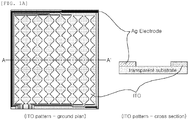
- Fig 1a is a cross-sectional view of a touch panel including ITO material according to the prior art
- Fig 1b and Fig. 1c are processes for manufacturing a touch panel including ITO material according to the prior art, which are flow charts of a photo etching process and a screen printing process, respectively.
- the touch screen using the capacitive way according to the prior art has poor touch sensitivity because sensing and motion sensors are formed by patterning ITO transparency electrode, so that it is not suitable for making a large area.
- an optical transmittance is not good and also visibility is bad due to the pattern of sensor electrode.
- the touch panel according to the prior art is manufactured by the photo etching process for forming a wiring and a pattern of ITO transparency electrode or a screen-printing process for forming a pattern of silver electrode.
- Patent KR10-2009-0015414 and US2002/0185981 disclose examples of these types of touch panel using pattern electrodes.
- the process is complex and the cost of manufacturing is high due to a photolithography process.
- the process is difficult to accurately control so that it is difficult to maintain an accurate align tolerance between ITO and outer electrode part; a line width is difficult to finely implement so that there are many dead spaces; a crack may be generated on the ITO micro line width part due to the high-temperature drying; and the cost of ITO material is high so that the cost for manufacturing the touch screen and touch pad including ITO material is high.
- An object of the present invention is to provide a capacitive touch panel and a method for manufacturing the same, in which the capacitive touch panel has an intaglio micro pattern formed by imprinting process and a conductive layer formed in the intaglio. with low resistance as compared with ITO, and various fill factors.
- Another object of the present invention is to provide a capacitive touch panel and a method for manufacturing the same, in which the capacitive touch panel is manufactured by forming a sensing electrode and a wiring electrode at the same time in the intaglio after processing the intaglio pattern on a resin layer laminated on a transparency substrate.
- Fig. 2a and Fig. 2b are plan views of a first sensing layer including a x-axis sensing electrode of an upper layer of a touch panel according to an embodiment of the present invention and of a second sensing layer including a y-axis sensing electrode of a lower layer of the touch panel, respectively.
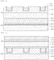
- Fig. 3 is a cross-sectional view along with a line A-A' of Fig. 2a and Fig. 4 is a cross-sectional view along with a line B-B' of Fig. 2a .
- Fig 5 shows a part of intaglio that is formed on a resin layer, in which the intaglio will be filled with sensing electrodes.
- the touch panel 10 is composed of a first sensing layer 100 including a plurality of first direction sensing electrodes 115 which are patterned and a plurality of first wiring electrodes 140, and a second sensing layer 200 including a plurality of second direction sensing electrodes 215 which are patterned and a plurality of second wiring electrodes 240.
- the plurality of the first wiring electrodes 140 and the plurality of the second wiring electrodes 240 are described in detail in Fig. 9 .
- the first sensing layer 100 and the second sensing layer 200 are formed by mutually bonding their broad sides in a vertical direction.
- One ends of the first direction sensing electrodes 115 are connected to the plurality of the first direction sensing electrodes lines D1L1, 2, 3..., and one ends of the second direction sensing electrodes 215 are connected to the plurality of the second direction sensing electrodes lines D2L1, 2, 3....
- the number of the plurality of the first and second directions sensing electrodes and the plurality of the first and second directions sensing electrodes lines may be determined widely and variously according to the uses of the touch panel.
- the first sensing layer 100 is the upper layer and the second sensing layer 200 is the lower layer. That is, the second sensing layer is firstly formed and the first sensing layer is formed on the second sensing layer.
- the material such as an adhesive, for example, OCA (Optical Clear Adhesive), and the like, which has an adhesive property, is included on the bottom part of the first sensing layer 100 without a separate bonding layer so that the first sensing layer is preferably bonded to the upper part of the second sensing layer 200.
- the bonding layer 300 in this situation is preferably Optical Clear Adhesive of a film type.
- the separate bonding layer 300 it is of great advantage in terms of insulating aspect.
- the touch panel may be formed by bonding any one of the sensing layers with the upper part or the bottom part of the other sensing layer after forming the first and second sensing layers at the same time.
- Each of the first direction sensing electrode 115 and the second direction sensing layer 215 is located on the first sensing layer 100 and the second sensing layer 200 to mutually cross in a space.
- the first direction sensing electrodes may be formed in a widthwise direction on the first sensing layer and the second direction sensing electrodes may be formed in a lengthwise direction on the second sensing layer.
- the first direction sensing electrodes are formed in a plurality of first regions R1 for sensing object's touch and a plurality of second regions R2 for connecting the first regions on the surface of the touch panel 10.
- the second direction sensing electrodes include a plurality of first regions R3 and a plurality of second regions R4, which have the same shape as the plurality of the first regions R1 and the plurality of the second regions R2, except in that the first regions R1 is formed in the lengthwise direction and the second regions R2 is formed in the widthwise direction on the first sensing layer.
- the first regions R1 of the first sensing layer sense positional information of a horizontal axis
- the first regions R3 of the second sensing layer performs the operation for sensing positional information of a vertical axis. Therefore, the touch point can be correctly found on the touch panel 10.
- the plurality of the first regions R1, R3 are preferably formed more broadly as compared with the plurality of the second regions R2, R4 for easily sensing the object that is touched on the surface of the touch panel.
- the plurality of the first regions R1, R3 and the plurality of the second regions R2, R4 may be formed to surround their edges by edge electrodes 115c.
- the plurality of the first regions R1 has various shapes, such as diamonds, hexagon, and the like, and sensing electrodes having a lattice shape form inside the regions. That is, as shown in Fig. 2a and Fig. 2b , a plurality of sensing electrodes 115a in a widthwise direction and a plurality of sensing electrode 115b in a lengthwise direction may be formed to cross mutually so that the first regions R1, R3 may be formed in a lattice shape.
- a crossing region 211c between an intaglio region 211a to be filled with widthwise direction electrodes and an intaglio region 211b to be filled with lengthwise direction electrodes among the electrodes composing the sensing electrodes is formed a little bit broadly than non-crossing regions 211a, 211b.
- the plurality of the first regions R1, R3 may not be overlapped mutually in a vertical direction of the first and second sensing layers and the plurality of the second regions R2, R4 may be overlapped in a vertical direction with the second region of the first sensing layer and the second region of the second sensing layer.
- each pattern of the second region R2 of the first sensing layer and the second region R4 of the second sensing layer may be formed in a different pattern from each pattern of the first region of the first sensing layer and the first region of the second sensing layer.
- the pattern formed by vertically overlapping the second region R2 of the first sensing layer and the second region R4 of the second sensing layer may preferably be formed to be the same or similar with the pattern of the first region of the first sensing layer or the pattern of the first region of the second sensing layer.
- An optical transmittance of the sensing layer can be improved by forming the sensing electrodes in a lattice shape of widthwise direction and lengthwise direction on the first sensing layer and the second sensing layer.
- the ends of the plurality of sensing electrodes 115b, 215a of lengthwise direction and the sensing electrodes 115a, 215d of widthwise direction are connected to edge electrodes 115c, 215c thereby preventing an increase of resistance capacity of the first regions R1, R3 so that a sufficient amount of current can be flowed into the first and second sensing electrodes of the first and second layers and then finally a touch sensitivity of the touch panel can be improved.
- the first region R1 of the first sensing layer 100 and the first region R3 of the second sensing layer 200 are arranged to not overlap mutually in a vertical direction of the first and second sensing layers. Looking the touch panel 10 down from the first sensing layer 100 that is the upper layer, the first region R1 of the first sensing layer 100 is projected onto the region 110 on which any sensing electrode on the second sensing layer 200 is not formed.
- the resin layers 110, 210 including the patterned layers on the transparent substrate 120 are laminated on the first sensing layer 100 and the second sensing layer 200 and an intaglio is formed inside thereof.
- the intaglio includes the seed layers 113, 213 and a metal layer for forming the sensing electrodes 115, 215 and the wiring electrodes 140, 240 inside thereof.
- the intaglio according to the present embodiment does not penetrate to the transparent substrate because the resin layers 110, 210 are still remained in the bottom part.
- the first sensing layer 100 and the second sensing layer 200 are bonded by the bonding layer 300.
- the patterned layer means the region formed with the intaglio on the resin layer according to the pattern of the sensing electrodes.
- Fig. 6 shows cross-sectional shapes of intaglio that are formed by molds having various shapes and relevant molds that are used for forming the intaglio on the patterned layer
- Fig. 7 is a plan view of the patterned layer on the intaglio that is formed by a mold having a square shape.
- the cross-section of the intaglio to be formed with the sensing electrodes on the resin layer 110 laminated on the transparent substrate 120 and the mold 400 forming the intaglio are shown.
- the cross-section of the intaglio may be a square, a triangle, and a diamond shapes.
- the width of the intaglio and the pitch that is an interval between the intaglios for forming a lattice pattern should have the value within a certain range as disclosed in Table 1 so that Fill Factor can be obtained.
- the depth of the intaglio may be formed to have the same height with the height of the resin layer to be formed, but a part of resin layer is still remained on the floor surface of the intaglio so that the surface of the transparent substrate and the metal layer should not preferably be contacted.
- the Fill Factor as defined above is less than 1.4, the optical transmittance is increased but the touch motion is possible to not smoothly perform due to the decrease of the contact area for capacitance and the increase of resistance of the conductive layer; and when the fill factor is above 10, there are disadvantages such that the pattern of the sensing electrodes is sighted and the transmittance is decreased due to the increase of the area of the conductive layer.
- the Fill Factor preferably has the value between 1.4 ⁇ 7.0 %, and the line width of the sensing electrodes and the pitch are preferably used by adjusting properly according to the value of the Fill Factor.
- Line Width Pitch Fill ( ⁇ m) ( ⁇ m) Factor (%) 1 ⁇ 5 100 1.9 ⁇ 10 200 2.5 ⁇ 5.0 300 1.9 ⁇ 3.5 400 1.4 ⁇ 2.5 500 0.4 ⁇ 1.9 600 0.3 ⁇ 1.7 6 ⁇ 10 100 11 ⁇ 19 200 5.9 ⁇ 10 300 3.9 ⁇ 7.0 400 2.9 ⁇ 5.0 500 2.3 ⁇ 3.9 600 1.9 ⁇ 3.3
- Fig. 8a to Fig. 8f show a process for forming sensing electrodes when the cross-section of the intaglio is a square in any sensing layer of a touch panel according an embodiment of the present invention
- Fig. 9 shows the sensing electrodes and the wiring electrodes together that are formed on the edge of the sensing layer
- Fig. 10 shows a process for removing the metallic material and the conductive polymer remained on the surface of the patterned layer except the sensing electrodes after coating the metallic material or the conductive polymer without the seed layer in the intaglio.
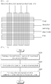
- Fig. 13 is a flow chart of method for manufacturing a touch panel according to an embodiment of the present invention
- Fig. 14 is a flow chart of a process for forming the sensing layer of Fig. 13 .
- the touch panel that is composed of the sensing layers is produced by the method comprising: forming the second sensing layer having the second sensing electrodes that are patterned in a second direction (S100); forming the bonding layer that is an adhesive (OCA) for bonding the first sensing layer on the surface of the second sensing layer (S200); and forming the first sensing layer having the first sensing electrodes that are patterned in a first direction on the surface of the bonding layer.
- S100 second direction
- OCA adhesive
- the adhesive is a film type, and preferably allows to bond the first and second sensing layers by laminating between the first sensing layer and the second sensing layer.
- the first sensing layer and the second sensing layer may be mutually bonded by including an adhesion material on the lower side of the upper layer. That is, any one sensing layer from the first and second sensing layers includes the material having an adhesion on the lower part thereof thereby having a role as the bonding layer without a separate bonding layer so that the thickness of the touch panel can be decreased.
- the first sensing layer and the second sensing layer are formed through the same process. Referring to Fig. 8a to Fig. 8f , the process for forming the sensing layer will be described in detail based on the second sensing layer.
- the resin layer 210 is laminated on the transparent substrate 220 (S110, S310).
- the resin film or glass can be used as the transparent substrate 220.
- thermoplastic resin such as polyethyleneterephthalate (PET), polycarbonate (PC), polymethylmetharylate (PMMA), triacetate cellulose (TAC), polyethersulfone (PES), and the like
- PET polyethyleneterephthalate
- PC polycarbonate
- PMMA polymethylmetharylate
- TAC triacetate cellulose
- PES polyethersulfone
- the material including an adhesive such as PSA (Pressure Sensitive Adhesive) can be used.
- UV curing resin or thermo-setting resin can be used as the resin layer 210.
- the intaglio 211 is formed by imprinting the mold 400 on the resin layer 210.
- the intaglio 211 is formed according to the pattern to be formed with the plurality of the first and second direction sensing electrodes and the plurality of the first and second wiring electrodes (S120, S320).
- the intaglio 211 may be formed by curing the resin layer 210 through giving UV or heat in a state of pressing the mold 400 on the resin material before curing the resin material, and then removing the mold 400 after curing the resin material.
- an embossed mold 300 is used for forming the intaglio on the resin layer 210, and is preferably the material having a quality of a sufficiently lower surface roughness. After pattering the intaglio according to the mold, it is preferable to have Haze of less than 4 %.
- a pattern type of the intaglio formed on the resin layer 210 according to the present embodiment is a square, but the cross-sectional shapes of the intaglio having various patterns can be obtained by using the molds having various shapes as shown in Fig. 6 .
- the pattern size of the intaglio formed on the resin layer 210 can be different according to the embodiments, but it preferably is that the line width of the electrode is 1 ⁇ m ⁇ 10 ⁇ m, the depth of the electrode is 1 ⁇ m ⁇ 10 ⁇ m, and the pitch between of the electrodes is 200 ⁇ m ⁇ 600 ⁇ m.
- the internal surface of the intaglio 211 and the surface of the resin layer 210 are preferably surface-treated in order to improve an adhesive property between the resin layer 210 and the seed layer 213 to be formed in the subsequent process, and the part that is surface-treated may be marked as the surface-treated layer 212 as shown in Fig. 8c (S130, S330).
- a method for surface-treating may include a chemical etching using alkali-based aqueous solution or catalyst treatments, and plasma or ion beam treatments, and the like.
- the metallic seed layer 213 is formed on the surface-treated layer 212 (S140, S340).
- the seed layer 213 may be formed by using an electroless plating, CVD deposition, sputtering or printing using a metal material.
- the material for the seed layer may include any one of copper (Cu), nickel (Ni), chromium (Cr), iron (Fe), tungsten (W), phosphorus (P), cobalt (Co), silver (Ag), silver-carbon (Ag-C), nickel-phosphorus (Ni-P), copper oxide II (CuO), and inorganic matter (SiO 2 ), or alloy thereof; and its thickness preferably is 0.01 ⁇ m ⁇ 5 ⁇ m.
- the process for removing the seed layer 213 from the surface of the resin layer other than the patterned region of the intaglio includes selectively removing (S160, S360) the resin that is filled inside the intaglio and the seed layer formed on the surface of the resin layer by depositing in an etching solution after filling (S150, S350) with the resin having an etch resistance inside the intaglio that is the patterned region.
- a chemical used for the etching includes any one of a type of nitric acid, a type of sulfuric acid, a type of hydrochloric acid, a type of copper sulphate, ferric chloride, and copper shloride.
- the sensing electrodes 215 and the wiring electrodes 240 may be formed by an electroless plating, an electro plating, CVD deposition, sputtering, coating or printing on the seed layer 213 (S170, S370).
- the sensing electrodes and the wiring electrodes are formed at the same time, and preferably by using the material having a lower resistance than ITO (Indume Tin Oxide).
- ITO Indume Tin Oxide
- any one of copper (Cu), silver (Ag), silver-carbon (Ag-C), aluminum (Al), nickel (Ni), chromium (Cr), and nickel-phosphorus (Ni-P), or alloy thereof can be used as the raw material for the sensing electrode 215 and the wiring electrode 240.
- each of the first and second wiring electrodes 140, 240 may be formed at the same time with each of the first and second direction sensing electrodes on the part of edge of each of the first and second sensing layers in a broader width than the width of each of the first and second direction sensing electrodes.
- the sensing layer may be formed by wiping or scratching with a blade 230 on the surface to be free of residue after coating the metallic material or conductive polymer without the metallic seed layer on the patterned layer (S180, S380).
- the conductive polymer coated on the surface of the patterned layer has a thickness of 1 ⁇ m-10 ⁇ m.
- the height of the metal layer filled on the intaglio pattern of the resin layer 210 is preferably the same or lower than the depth of the intaglio pattern formed on the resin layer 210.
- the pattern of the sensing electrodes of the touch panel is only an embodiment, but a plurality of the sensing electrodes that perform the functions of sensing and operating of the touch may be patterned in various structures and then applied.
- the pattern of the sensing electrode as mentioned above relates to the Fill Factor that is calculated as a ratio of the area the patterned layer formed with the sensing electrodes to the area of the sensing electrodes, and the Fill Factor of the touch panel according to the present embodiment is disclosed in Table 1.
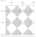
- Fig. 11 is a plan view of any sensing layer having the sensing electrodes that are formed on the touch panel according to another embodiment of the present invention
- Fig. 12 is a plan view of sensing electrodes that are formed on the touch panel according another embodiment of the present invention.
- Fig. 11 is an embodiment applied with the structure of a minimized sight clearance by removing the edge electrode formed outside of the sensing and operating regions of the sensing electrodes of Fig. 2a and Fig. 2b , and even in this situation, the Fill Factor in the cross region between the widthwise sensing electrode and the lengthwide sensing electrode formed on the same sensing layer is the same with Table 1.
- Fig. 12 shows a plurality of fine sensing elecrodes in a vertical or horizontal direction on each sensing layer, and the sensing electrodes on the different sensing layer each other on the plan view of the touch panel are displayed in a lattice shape that are intersected in X and Y axis.
- the Fill Factor on the part in which the sensing electrode lines are intersected in X and Y-axis is the same with Table 1.
- the above structure has an advantage structure in terms of the sight clearance of the sensing electrodes as compared with the shape of the sensing electrodes having the edge electrodes as disclosed in Fig. 2a and Fig. 2b .
- the sensing electrode may have various Fill Factors for the line width and pitch of the sensing electordes, and also the sensing electrodes can be composed in various shapes of their section, such as a square, a pentagon, a hexagon, an oval, and the like.
- the capacitive touch panel and method for manufacturing the same can provide the touch panel having various Fill Factors that are formed with the conductive layer having a low resistance as compared with ITO on the intaglio after a fine pattern of the intaglio applied with the imprinting process, thereby improving the touch sensitivity and performance and also making a large area.
- the capacitive touch panel and method for manufacturing the same according to the present embodiment can improve the optical transmittance that can be limited due to the sensing electrode and also the sight clearance by arranging the sensing electrode in a lattice shape.
- the capacitive touch panel and method for manufacturing the same according to the present embodiment can provide an excellent durability by preventing an exposure of the electrode part by forming the electrode part on the intaglio.
- the capacitive touch panel and method for manufacturing the same can reduce the time and the process for manufacturing, and also increase productivity and reduce the cost for manufacturing by forming the sensing electrode and the wiring electrode at the same time on the intaglio of the fine pattern formed on the resin layer.
Description
- The present invention relates to a touch panel, and more specifically, to a capacitive touch panel and a method for manufacturing the same.
- A touch screen device means an input unit for performing the whole control of an electronic device; comprising controlling a display screen by sensing a touch point of user on the display screen and then using the information about the sensible touch point as input information.
- The touch screen device uses a touch screen, such as a resistive touch screen, a capacitive touch screen, an ultrasonic touch screen, an optical (infrared) sensor touch screen, an electron inducing touch screen, and the like. They have different characteristics, such as signal amplification, a resolution, the level of difficulty of plan and process technology, and the like, according to each way. Therefore, the touch screen device has to reflect and select enough to be able to emphasize each way's advantage.
- For specifically selecting a way, durability, an economic feasibility, and the like should be considered in addition to an optical property, a technical property, and an input property. Two representative ways from among these are the resistive way and the capacitive way. From among these, the capacitive touch screen that is applied to Mobile, MP2 device, Note Book, and the like, generally uses ITO (Indume Tin Oxide) transparency electrode.
-
Fig 1a is a cross-sectional view of a touch panel including ITO material according to the prior art;Fig 1b andFig. 1c are processes for manufacturing a touch panel including ITO material according to the prior art, which are flow charts of a photo etching process and a screen printing process, respectively. - Referring to
Fig. 1a , the touch screen using the capacitive way according to the prior art has poor touch sensitivity because sensing and motion sensors are formed by patterning ITO transparency electrode, so that it is not suitable for making a large area. In addition, an optical transmittance is not good and also visibility is bad due to the pattern of sensor electrode. - Referring to
Fig. 1b and1c , the touch panel according to the prior art is manufactured by the photo etching process for forming a wiring and a pattern of ITO transparency electrode or a screen-printing process for forming a pattern of silver electrode. PatentKR10-2009-0015414 US2002/0185981 disclose examples of these types of touch panel using pattern electrodes. - In the case of the photo etching process, the process is complex and the cost of manufacturing is high due to a photolithography process. In the case of the screen-printing process, the process is difficult to accurately control so that it is difficult to maintain an accurate align tolerance between ITO and outer electrode part; a line width is difficult to finely implement so that there are many dead spaces; a crack may be generated on the ITO micro line width part due to the high-temperature drying; and the cost of ITO material is high so that the cost for manufacturing the touch screen and touch pad including ITO material is high.
- An object of the present invention is to provide a capacitive touch panel and a method for manufacturing the same, in which the capacitive touch panel has an intaglio micro pattern formed by imprinting process and a conductive layer formed in the intaglio. with low resistance as compared with ITO, and various fill factors.
- Another object of the present invention is to provide a capacitive touch panel and a method for manufacturing the same, in which the capacitive touch panel is manufactured by forming a sensing electrode and a wiring electrode at the same time in the intaglio after processing the intaglio pattern on a resin layer laminated on a transparency substrate.
- In order to achieve the above objects, a capacitive touch panel according to the invention is disclosed in the claims.
- The above and other objects, features and advantages of the present invention will become apparent from the following description of the examples given in conjunction with the accompanying drawings, in which:
-
Fig. 1a is a cross-sectional view of a touch panel including ITO material according to the prior art, andFig. 1b andFig. 1c are flow charts of a photo etching process and a screen printing process for manufacturing a touch panel including ITO material according to the prior art, respectively. -
Fig. 2a andFig. 2b are plan views of a first sensing layer including a x-axis sensing electrode of an upper layer of a touch panel according to an embodiment of the present invention and of a second sensing layer including a y-axis sensing electrode of a lower layer of the touch panel, respectively. -
Fig. 3 is a cross-sectional view along with a line A-A' ofFig. 2a . -
Fig. 4 is a cross-sectional view along with a line B-B' ofFig. 2a . -
Fig 5 shows a part of intaglio that is formed on a resin layer, in which the intaglio will be filled with sensing electrodes. -
Fig. 6 shows shapes of intaglio that are formed by molds having various shapes and relevant molds that are used for forming the intaglio on the patterned layer. -
Fig. 7 is a plan view of the patterned layer formed on the intaglio formed by a mold having a square shape. -
Fig. 8a to Fig. 8f show a process for forming sensing electrodes when the cross-section of the intaglio is a square in any sensing layer of a touch panel according to an embodiment of the present invention. -
Fig. 9 is a cross-sectional view along with a line C-C' ofFig. 2a , showing the sensing electrodes and the wiring electrodes together formed on the edge of the sensing layer. -
Fig. 10 shows a process for removing a metallic material or a conductive polymer remained on the surface of the patterned layer except the sensing electrodes after coating the metallic material or the conductive polymer without a seed layer in the intaglio. -
Fig. 11 is a plan view of any sensing layer having the sensing electrodes that are formed on the touch panel according to another embodiment of the present invention. -
Fig. 12 is a plan view of sensing electrodes that are formed on the touch panel according another embodiment of the present invention. -
Fig. 13 is a flow chart of method for manufacturing the touch panel according to an embodiment of the present invention. -
Fig. 14 is a flow chart of a process for forming the sensing layer ofFig. 13 . - Hereinafter, the embodiments of the present invention will be described in detail with reference to accompanying drawings. First of all, for adding a reference mark to component parts in each of figures, it must be given attention to have same marks, if possible, for the same component part, even if marking in other figures. In addition, for describing the present invention, when it is considered that the specific descriptions about the relevant known constitutions or functions may hurt the point of the present invention, the detailed descriptions will be omitted, and the terms that are in the singular may include a pluralized concept. In addition, hereinafter, the preferable embodiments of the present invention will be described, but the present invention is not limited thereto and of course, may be performed by variously modifying by the person who has a skill in the art without the limitation.
-
Fig. 2a andFig. 2b are plan views of a first sensing layer including a x-axis sensing electrode of an upper layer of a touch panel according to an embodiment of the present invention and of a second sensing layer including a y-axis sensing electrode of a lower layer of the touch panel, respectively.Fig. 3 is a cross-sectional view along with a line A-A' ofFig. 2a andFig. 4 is a cross-sectional view along with a line B-B' ofFig. 2a .Fig 5 shows a part of intaglio that is formed on a resin layer, in which the intaglio will be filled with sensing electrodes. - Referring to
Fig. 2a to Fig. 4 , thetouch panel 10 according to an embodiment of the present invention is composed of afirst sensing layer 100 including a plurality of firstdirection sensing electrodes 115 which are patterned and a plurality offirst wiring electrodes 140, and asecond sensing layer 200 including a plurality of seconddirection sensing electrodes 215 which are patterned and a plurality ofsecond wiring electrodes 240. Here, the plurality of thefirst wiring electrodes 140 and the plurality of thesecond wiring electrodes 240 are described in detail inFig. 9 . Thefirst sensing layer 100 and thesecond sensing layer 200 are formed by mutually bonding their broad sides in a vertical direction. One ends of the firstdirection sensing electrodes 115 are connected to the plurality of the first direction sensing electrodes lines D1L1, 2, 3..., and one ends of the seconddirection sensing electrodes 215 are connected to the plurality of the second direction sensing electrodes lines D2L1, 2, 3.... - Here, the number of the plurality of the first and second directions sensing electrodes and the plurality of the first and second directions sensing electrodes lines may be determined widely and variously according to the uses of the touch panel.
- For the embodiments, the
first sensing layer 100 is the upper layer and thesecond sensing layer 200 is the lower layer. That is, the second sensing layer is firstly formed and the first sensing layer is formed on the second sensing layer. In this situation, the material, such as an adhesive, for example, OCA (Optical Clear Adhesive), and the like, which has an adhesive property, is included on the bottom part of thefirst sensing layer 100 without a separate bonding layer so that the first sensing layer is preferably bonded to the upper part of thesecond sensing layer 200. - However, when it is possible to bond the
first sensing layer 100 and thesecond sensing layer 200 by forming theseparate bonding layer 300 theirbetween, thebonding layer 300 in this situation is preferably Optical Clear Adhesive of a film type. In the case of using theseparate bonding layer 300 as mentioned above, it is of great advantage in terms of insulating aspect. - In addition, the touch panel may be formed by bonding any one of the sensing layers with the upper part or the bottom part of the other sensing layer after forming the first and second sensing layers at the same time.
- Each of the first
direction sensing electrode 115 and the seconddirection sensing layer 215 is located on thefirst sensing layer 100 and thesecond sensing layer 200 to mutually cross in a space. For example, the first direction sensing electrodes may be formed in a widthwise direction on the first sensing layer and the second direction sensing electrodes may be formed in a lengthwise direction on the second sensing layer. - The first direction sensing electrodes are formed in a plurality of first regions R1 for sensing object's touch and a plurality of second regions R2 for connecting the first regions on the surface of the
touch panel 10. The second direction sensing electrodes include a plurality of first regions R3 and a plurality of second regions R4, which have the same shape as the plurality of the first regions R1 and the plurality of the second regions R2, except in that the first regions R1 is formed in the lengthwise direction and the second regions R2 is formed in the widthwise direction on the first sensing layer. - However, the first regions R1 of the first sensing layer sense positional information of a horizontal axis, but the first regions R3 of the second sensing layer performs the operation for sensing positional information of a vertical axis. Therefore, the touch point can be correctly found on the
touch panel 10. - The plurality of the first regions R1, R3 are preferably formed more broadly as compared with the plurality of the second regions R2, R4 for easily sensing the object that is touched on the surface of the touch panel.
- The plurality of the first regions R1, R3 and the plurality of the second regions R2, R4 may be formed to surround their edges by
edge electrodes 115c. The plurality of the first regions R1 has various shapes, such as diamonds, hexagon, and the like, and sensing electrodes having a lattice shape form inside the regions. That is, as shown inFig. 2a andFig. 2b , a plurality ofsensing electrodes 115a in a widthwise direction and a plurality ofsensing electrode 115b in a lengthwise direction may be formed to cross mutually so that the first regions R1, R3 may be formed in a lattice shape. - As shown in
Fig. 5 , acrossing region 211c between anintaglio region 211a to be filled with widthwise direction electrodes and anintaglio region 211b to be filled with lengthwise direction electrodes among the electrodes composing the sensing electrodes is formed a little bit broadly thannon-crossing regions - Preferably, the plurality of the first regions R1, R3 may not be overlapped mutually in a vertical direction of the first and second sensing layers and the plurality of the second regions R2, R4 may be overlapped in a vertical direction with the second region of the first sensing layer and the second region of the second sensing layer.
- As other embodiment, each pattern of the second region R2 of the first sensing layer and the second region R4 of the second sensing layer may be formed in a different pattern from each pattern of the first region of the first sensing layer and the first region of the second sensing layer. At this situation, the pattern formed by vertically overlapping the second region R2 of the first sensing layer and the second region R4 of the second sensing layer may preferably be formed to be the same or similar with the pattern of the first region of the first sensing layer or the pattern of the first region of the second sensing layer.
- An optical transmittance of the sensing layer can be improved by forming the sensing electrodes in a lattice shape of widthwise direction and lengthwise direction on the first sensing layer and the second sensing layer. In addition, the ends of the plurality of
sensing electrodes sensing electrodes electrodes - The first region R1 of the
first sensing layer 100 and the first region R3 of thesecond sensing layer 200 are arranged to not overlap mutually in a vertical direction of the first and second sensing layers. Looking thetouch panel 10 down from thefirst sensing layer 100 that is the upper layer, the first region R1 of thefirst sensing layer 100 is projected onto theregion 110 on which any sensing electrode on thesecond sensing layer 200 is not formed. - Referring to
Fig. 3 and Fig. 4 , and the sections on A-A' and B-B' of thetouch panel 10 ofFigs. 2a and2b , the resin layers 110, 210 including the patterned layers on thetransparent substrate 120 are laminated on thefirst sensing layer 100 and thesecond sensing layer 200 and an intaglio is formed inside thereof. The intaglio includes the seed layers 113, 213 and a metal layer for forming thesensing electrodes wiring electrodes first sensing layer 100 and thesecond sensing layer 200 are bonded by thebonding layer 300. - Here, the patterned layer means the region formed with the intaglio on the resin layer according to the pattern of the sensing electrodes.
-
Fig. 6 shows cross-sectional shapes of intaglio that are formed by molds having various shapes and relevant molds that are used for forming the intaglio on the patterned layer, andFig. 7 is a plan view of the patterned layer on the intaglio that is formed by a mold having a square shape. - Referring to
Fig. 6 , the cross-section of the intaglio to be formed with the sensing electrodes on theresin layer 110 laminated on thetransparent substrate 120 and themold 400 forming the intaglio are shown. For example, the cross-section of the intaglio may be a square, a triangle, and a diamond shapes. Even though the intaglio has various shapes, the width of the intaglio and the pitch that is an interval between the intaglios for forming a lattice pattern should have the value within a certain range as disclosed in Table 1 so that Fill Factor can be obtained. The depth of the intaglio may be formed to have the same height with the height of the resin layer to be formed, but a part of resin layer is still remained on the floor surface of the intaglio so that the surface of the transparent substrate and the metal layer should not preferably be contacted. - Referring to
Fig. 7 andEquation 1, the Fill Factor is defined as a ratio dividing the area of a lattice shape that is formed on one sensing layer by the area of the conductive layer, and is presented by the following Equation 1:
- When the Fill Factor as defined above is less than 1.4, the optical transmittance is increased but the touch motion is possible to not smoothly perform due to the decrease of the contact area for capacitance and the increase of resistance of the conductive layer; and when the fill factor is above 10, there are disadvantages such that the pattern of the sensing electrodes is sighted and the transmittance is decreased due to the increase of the area of the conductive layer.
- Therefore, the Fill Factor preferably has the value between 1.4∼7.0 %, and the line width of the sensing electrodes and the pitch are preferably used by adjusting properly according to the value of the Fill Factor.
[Table 1] Line Width Pitch Fill (µm) (µm) Factor (%) 1 ∼ 5 100 1.9 ∼ 10 200 2.5 ∼ 5.0 300 1.9 ∼ 3.5 400 1.4 ∼ 2.5 500 0.4 ∼ 1.9 600 0.3 ∼ 1.7 6 ∼ 10 100 11 ∼ 19 200 5.9 ∼ 10 300 3.9 ∼ 7.0 400 2.9 ∼ 5.0 500 2.3 ∼ 3.9 600 1.9 ∼ 3.3 -
Fig. 8a to Fig. 8f show a process for forming sensing electrodes when the cross-section of the intaglio is a square in any sensing layer of a touch panel according an embodiment of the present invention;Fig. 9 shows the sensing electrodes and the wiring electrodes together that are formed on the edge of the sensing layer; andFig. 10 shows a process for removing the metallic material and the conductive polymer remained on the surface of the patterned layer except the sensing electrodes after coating the metallic material or the conductive polymer without the seed layer in the intaglio.Fig. 13 is a flow chart of method for manufacturing a touch panel according to an embodiment of the present invention; andFig. 14 is a flow chart of a process for forming the sensing layer ofFig. 13 . - Firstly, referring to
Fig. 13 to Fig. 14 , according to the method for manufacturing the touch panel according to the embodiment of the present invention, the touch panel that is composed of the sensing layers is produced by the method comprising: forming the second sensing layer having the second sensing electrodes that are patterned in a second direction (S100); forming the bonding layer that is an adhesive (OCA) for bonding the first sensing layer on the surface of the second sensing layer (S200); and forming the first sensing layer having the first sensing electrodes that are patterned in a first direction on the surface of the bonding layer. - The adhesive is a film type, and preferably allows to bond the first and second sensing layers by laminating between the first sensing layer and the second sensing layer.
- For another embodiment, the first sensing layer and the second sensing layer may be mutually bonded by including an adhesion material on the lower side of the upper layer. That is, any one sensing layer from the first and second sensing layers includes the material having an adhesion on the lower part thereof thereby having a role as the bonding layer without a separate bonding layer so that the thickness of the touch panel can be decreased.
- For the present embodiment, the first sensing layer and the second sensing layer are formed through the same process. Referring to
Fig. 8a to Fig. 8f , the process for forming the sensing layer will be described in detail based on the second sensing layer. - Referring to
Fig. 8a to Fig. 8f , theresin layer 210 is laminated on the transparent substrate 220 (S110, S310). The resin film or glass can be used as thetransparent substrate 220. - When using the resin film, a thermoplastic resin, such as polyethyleneterephthalate (PET), polycarbonate (PC), polymethylmetharylate (PMMA), triacetate cellulose (TAC), polyethersulfone (PES), and the like, can be used; its thickness is suitably the range of 25∼250 µm; and the optical transmittance is suitably above 80 %, more preferably above 90 %. When using the resin film as the transparent substrate, the material including an adhesive, such as PSA (Pressure Sensitive Adhesive) can be used.
- UV curing resin or thermo-setting resin can be used as the
resin layer 210. - And then, as shown in
Fig. 8b , theintaglio 211 is formed by imprinting themold 400 on theresin layer 210. Theintaglio 211 is formed according to the pattern to be formed with the plurality of the first and second direction sensing electrodes and the plurality of the first and second wiring electrodes (S120, S320). When UV curing resin or thermo-setting resin is used as the material for theresin layer 210, theintaglio 211 may be formed by curing theresin layer 210 through giving UV or heat in a state of pressing themold 400 on the resin material before curing the resin material, and then removing themold 400 after curing the resin material. - At this time, an embossed
mold 300 is used for forming the intaglio on theresin layer 210, and is preferably the material having a quality of a sufficiently lower surface roughness. After pattering the intaglio according to the mold, it is preferable to have Haze of less than 4 %. - As shown in
Fig. 8b , a pattern type of the intaglio formed on theresin layer 210 according to the present embodiment is a square, but the cross-sectional shapes of the intaglio having various patterns can be obtained by using the molds having various shapes as shown inFig. 6 . The pattern size of the intaglio formed on theresin layer 210 can be different according to the embodiments, but it preferably is that the line width of the electrode is 1µm∼10µm, the depth of the electrode is 1µm∼10µm, and the pitch between of the electrodes is 200µm∼600µm. - And then, the internal surface of the
intaglio 211 and the surface of theresin layer 210 are preferably surface-treated in order to improve an adhesive property between theresin layer 210 and theseed layer 213 to be formed in the subsequent process, and the part that is surface-treated may be marked as the surface-treatedlayer 212 as shown inFig. 8c (S130, S330). A method for surface-treating may include a chemical etching using alkali-based aqueous solution or catalyst treatments, and plasma or ion beam treatments, and the like. - And then, as shown in
Fig. 8d , themetallic seed layer 213 is formed on the surface-treated layer 212 (S140, S340). Theseed layer 213 may be formed by using an electroless plating, CVD deposition, sputtering or printing using a metal material. The material for the seed layer may include any one of copper (Cu), nickel (Ni), chromium (Cr), iron (Fe), tungsten (W), phosphorus (P), cobalt (Co), silver (Ag), silver-carbon (Ag-C), nickel-phosphorus (Ni-P), copper oxide II (CuO), and inorganic matter (SiO2), or alloy thereof; and its thickness preferably is 0.01µm~5µm. - Referring to
Fig. 8e , the process for removing theseed layer 213 from the surface of the resin layer other than the patterned region of the intaglio includes selectively removing (S160, S360) the resin that is filled inside the intaglio and the seed layer formed on the surface of the resin layer by depositing in an etching solution after filling (S150, S350) with the resin having an etch resistance inside the intaglio that is the patterned region. In this situation, a chemical used for the etching includes any one of a type of nitric acid, a type of sulfuric acid, a type of hydrochloric acid, a type of copper sulphate, ferric chloride, and copper shloride. - Referring to
Fig. 8f , thesensing electrodes 215 and thewiring electrodes 240 may be formed by an electroless plating, an electro plating, CVD deposition, sputtering, coating or printing on the seed layer 213 (S170, S370). The sensing electrodes and the wiring electrodes are formed at the same time, and preferably by using the material having a lower resistance than ITO (Indume Tin Oxide). Especially, any one of copper (Cu), silver (Ag), silver-carbon (Ag-C), aluminum (Al), nickel (Ni), chromium (Cr), and nickel-phosphorus (Ni-P), or alloy thereof can be used as the raw material for thesensing electrode 215 and thewiring electrode 240. - Referring to
Fig. 9 , each of the first andsecond wiring electrodes - Referring to
Fig. 10 , as other embodiment, the sensing layer may be formed by wiping or scratching with ablade 230 on the surface to be free of residue after coating the metallic material or conductive polymer without the metallic seed layer on the patterned layer (S180, S380). In this situation, the conductive polymer coated on the surface of the patterned layer has a thickness of 1µm-10µm. The height of the metal layer filled on the intaglio pattern of theresin layer 210 is preferably the same or lower than the depth of the intaglio pattern formed on theresin layer 210. - The pattern of the sensing electrodes of the touch panel is only an embodiment, but a plurality of the sensing electrodes that perform the functions of sensing and operating of the touch may be patterned in various structures and then applied. The pattern of the sensing electrode as mentioned above relates to the Fill Factor that is calculated as a ratio of the area the patterned layer formed with the sensing electrodes to the area of the sensing electrodes, and the Fill Factor of the touch panel according to the present embodiment is disclosed in Table 1.
-
Fig. 11 is a plan view of any sensing layer having the sensing electrodes that are formed on the touch panel according to another embodiment of the present invention, andFig. 12 is a plan view of sensing electrodes that are formed on the touch panel according another embodiment of the present invention. -
Fig. 11 is an embodiment applied with the structure of a minimized sight clearance by removing the edge electrode formed outside of the sensing and operating regions of the sensing electrodes ofFig. 2a andFig. 2b , and even in this situation, the Fill Factor in the cross region between the widthwise sensing electrode and the lengthwide sensing electrode formed on the same sensing layer is the same with Table 1. -
Fig. 12 shows a plurality of fine sensing elecrodes in a vertical or horizontal direction on each sensing layer, and the sensing electrodes on the different sensing layer each other on the plan view of the touch panel are displayed in a lattice shape that are intersected in X and Y axis. In this situation, the Fill Factor on the part in which the sensing electrode lines are intersected in X and Y-axis is the same with Table 1. The above structure has an advantage structure in terms of the sight clearance of the sensing electrodes as compared with the shape of the sensing electrodes having the edge electrodes as disclosed inFig. 2a andFig. 2b . - With the above method, the sensing electrode may have various Fill Factors for the line width and pitch of the sensing electordes, and also the sensing electrodes can be composed in various shapes of their section, such as a square, a pentagon, a hexagon, an oval, and the like.
- The capacitive touch panel and method for manufacturing the same according to the present embodiment can provide the touch panel having various Fill Factors that are formed with the conductive layer having a low resistance as compared with ITO on the intaglio after a fine pattern of the intaglio applied with the imprinting process, thereby improving the touch sensitivity and performance and also making a large area.
- The capacitive touch panel and method for manufacturing the same according to the present embodiment can improve the optical transmittance that can be limited due to the sensing electrode and also the sight clearance by arranging the sensing electrode in a lattice shape.
- The capacitive touch panel and method for manufacturing the same according to the present embodiment can provide an excellent durability by preventing an exposure of the electrode part by forming the electrode part on the intaglio.
- The capacitive touch panel and method for manufacturing the same according to the present embodiment can reduce the time and the process for manufacturing, and also increase productivity and reduce the cost for manufacturing by forming the sensing electrode and the wiring electrode at the same time on the intaglio of the fine pattern formed on the resin layer.
- The above explanation is only for illustrating by example of the present invention, and the person who has a general skill in the art can modify, amend and substitute variously within the range of the essential features of the present invention. Therefore, the embodiments disclosed in the present invention and the accompanying figures are for illustrating, not limiting the invention, and the range of the present invention will not be limited according to the embodiments and the accompanying figures. The protection range of the present invention should be interpreted according to the following claims.
Claims (11)
- A capacitive touch panel (10), comprising a first sensing layer (100) formed with a plurality of first direction sensing electrodes (115), and a plurality of first wiring electrodes (140); and a second sensing layer (200) formed with a plurality of second direction sensing electrodes (215), and a plurality of second wiring electrodes (240),
wherein the first sensing layer (100) and the second sensing layer (200) are mutually bonded in a vertical direction, and at least one of the first direction sensing electrodes (115) and the second direction sensing electrodes (215) is formed in a plurality of first regions (R1, R3) for sensing user's touch and a plurality of second regions (R2, R4) for connecting the first regions,
characterized in that the plurality of first direction sensing electrodes (115) and the plurality of second direction sensing electrodes (215) are each formed by a plurality of sensing electrodes (115a, 115b, 215a, 215d) having a line width arranged in accordance with a predetermined pattern,
wherein each of the first sensing layer (100) and the second sensing layer (200) includes a transparent substrate (120, 220), and a resin layer (110, 210) laminated on the transparent substrate (120, 220), wherein the resin layer (110, 210) has a patterned layer that is formed with patterned intaglio by imprinting on a surface of the resin layer (110, 210), wherein the sensing electrodes are formed in said intaglio using a conductive material having a resistance lower than Indium Tin Oxide,
wherein the plurality of first regions (R1, R3) and the plurality of second regions (R2, R4) are sensing and operating regions of the sensing electrodes (115, 215),
wherein edge electrodes (115c, 215c) formed outside of the sensing and operating regions of the sensing electrodes (115, 215) are absent,
wherein the plurality of first regions (R1, R3) comprises first regions (R1) on the first sensing layer (100), each formed by a plurality of sensing electrodes (115a) as well as by a plurality of sensing electrodes (115b), and first regions (R3) on the second sensing layer (200), each formed by a plurality of sensing electrodes (215d) as well as by a plurality of sensing electrodes (215a),
wherein the plurality of sensing electrodes (115a) of the first regions (R1) on the first sensing layer (100) and the plurality of sensing electrodes (115b) of the first regions (R1) on the first sensing layer (100) are formed to mutually cross each other and wherein the plurality of sensing electrodes (215d) of the first regions (R3) on the second sensing layer (200) and the plurality of sensing electrodes (215a) of the first regions (R3) on the second sensing layer (200) are formed to mutually cross each other,
wherein the plurality of second regions (R2, R4) comprises second regions (R2) on the first sensing layer (100), each formed by some of the plurality of sensing electrodes, and second regions (R4) on the second sensing layer (200), each formed by some of the plurality of sensing electrodes,
wherein some of the plurality of sensing electrodes formed in the second regions (R2) connect some of the plurality of sensing electrodes (115a) formed in the first regions (R1) with neighbor of some of the plurality of sensing electrodes (115a) formed in the first regions (R1),
wherein some of the plurality of sensing electrodes formed in the second regions (R4) connect some of the plurality of sensing electrodes (215a) formed in the first regions (R3) with neighbor of some of the plurality of sensing electrodes (215a) formed in the first regions (R3). - The capacitive touch panel (10) according to claim 1, wherein the plurality of first regions (R1, R3) are formed more broadly as compared with the plurality of second regions (R2, R4), respectively.
- The capacitive touch panel (10) according to claim 1, wherein the first region (R1) of the first sensing layer (100) and the first region (R3) of the second sensing layer (200) are mutually not overlapped in the vertical direction of the first and the second sensing layers (100, 200).
- The capacitive touch panel (10) according to claim 3, wherein the second region (R2) of the first sensing layer (100) and the second region (R4) of the second sensing layer (200) are overlapped in the vertical direction of the first and the second sensing layers (100, 200).
- The capacitive touch panel (10) according to claim 4, wherein a pattern formed by overlapping in the vertical direction of the second region (R2) of the first sensing layer (100) and the second region (R4) of the second sensing layer (200) is the same or similar with the pattern of the first region (R1) of the first sensing layer (100) or the pattern of the first region (R3) of the second sensing layer (200).
- The capacitive touch panel (10) according to claim 1, wherein the sensing electrode (115, 215) and the wiring electrode (140, 240) are formed inside the intaglio at the same time.
- The capacitive touch panel (10) according to claim 1, wherein the patterned layer is formed in a plurality of the intaglio having width of 1µm∼10µm, depth of 1µm∼10µm, and pitch of 200µm-600 µm, and the sensing electrode (115, 215) and the wiring electrode (140, 240) are any one of Cu, Ag, Ag-C, Al, Ni, Cr, and Ni-P, or an alloy thereof.
- The capacitive touch panel (10) according to claim 1, wherein the touch panel (10) has optical transmittance of above 80% and a haze of less than 4%.
- The capacitive touch panel (10) according to claim 1, wherein each of the first and second wiring electrodes (140, 240) is simultaneously formed in connection with each of the first and second direction sensing electrodes (115, 215) at a part of edges of each of the first and second sensing layers (100, 200), the first and second wiring electrodes (140, 240) having a wider width than the line width of the sensing electrodes of each of the first and second direction sensing electrodes (115, 215).
- A method for manufacturing a capacitive touch panel (10), comprising:forming (S100) a second sensing layer (200) having second wiring electrodes (240) and second sensing electrodes (215) that are patterned in a second direction; and forming (S300) a first sensing layer (100) having first wiring electrodes (140) and first sensing electrodes (115) that are patterned in a first direction, wherein the first sensing layer (100) is bonded on an upper surface or a lower surface of the second sensing layer (200),characterized in that the plurality of first direction sensing electrodes (115) and the plurality of second direction sensing electrodes (215) are each formed by a plurality of sensing electrodes (115a, 115b, 215a, 215d) having a line width arranged in accordance with a predetermined pattern,wherein each of the first sensing layer (100) and the second sensing layer (200) includes a transparent substrate (120, 220), and a resin layer (110, 210) laminated on the transparent substrate (120, 220), wherein the resin layer (110, 210) has a patterned layer that is formed with patterned intaglio by imprinting on a surface of the resin layer (110, 210), wherein the sensing electrodes are formed in said intaglio using a conductive material having a resistance lower than Indium Tin Oxide,wherein the plurality of first regions (R1, R3) and the plurality of second regions (R2, R4) are sensing and operating regions of the sensing electrodes (115, 215),wherein edge electrodes (115c, 215c) formed outside of the sensing and operating regions of the sensing electrodes (115, 215) are absent,wherein the plurality of first regions (R1, R3) comprises first regions (R1) on the first sensing layer (100), each formed by a plurality of sensing electrodes (115a) as well as by a plurality of sensing electrodes (115b), and first regions (R3) on the second sensing layer (200), each formed by a plurality of sensing electrodes (215d) as well as by a plurality of sensing electrodes (215a),wherein the plurality of sensing electrodes (115a) of the first regions (R1) on the first sensing layer (100) and the plurality of sensing electrodes (115b) of the first regions (R1) on the first sensing layer (100) are formed to mutually cross each other and wherein the plurality of sensing electrodes (215d) of the first regions (R3) on the second sensing layer (200) and the plurality of sensing electrodes (215a) of the first regions (R3) on the second sensing layer (200) are formed to mutually cross each other,wherein the plurality of second regions (R2, R4) comprises second regions (R2) on the first sensing layer (100), each formed by some of the plurality of sensing electrodes, and second regions (R4) on the second sensing layer (200), each formed by some of the plurality of sensing electrodes,wherein some of the plurality of sensing electrodes formed in the second regions (R2) connect some of the plurality of sensing electrodes (115a) formed in the first regions (R1) with neighbor of some of the plurality of sensing electrodes (115a) formed in the first regions (R1),wherein some of the plurality of sensing electrodes formed in the second regions (R4) connect some of the plurality of sensing electrodes (215a) formed in the first regions (R3) with neighbor of some of the plurality of sensing electrodes (215a) formed in the first regions (R3).
- The method for manufacturing the capacitive touch panel (10) according to claim 10, wherein at each of the forming (S100, S300) the first and second sensing layers (100, 200), each of the first and second wiring electrodes (140, 240) is simultaneously formed in connection with each of the first and second direction sensing electrodes (115, 215) at a part of edges of each of the first and second sensing layers (100, 200), the first and second wiring electrodes (140, 240) having a wider width than the line width of the sensing electrodes of each of the first and second direction sensing electrodes (115, 215).
Applications Claiming Priority (3)
| Application Number | Priority Date | Filing Date | Title |
|---|---|---|---|
| KR1020100019102A KR20110100034A (en) | 2010-03-03 | 2010-03-03 | Electrostatic capacity type touch panel and manufacuring method thereof |
| KR1020100076269A KR101728818B1 (en) | 2010-08-09 | 2010-08-09 | Electrostatic capacity type touch panel and manufacturing method thereof |
| PCT/KR2011/001478 WO2011108869A2 (en) | 2010-03-03 | 2011-03-03 | Capacitive touch panel and manufacturing method for same |
Publications (3)
| Publication Number | Publication Date |
|---|---|
| EP2544080A2 EP2544080A2 (en) | 2013-01-09 |
| EP2544080A4 EP2544080A4 (en) | 2016-05-18 |
| EP2544080B1 true EP2544080B1 (en) | 2019-08-28 |
Family
ID=44542728
Family Applications (1)
| Application Number | Title | Priority Date | Filing Date |
|---|---|---|---|
| EP11750926.5A Active EP2544080B1 (en) | 2010-03-03 | 2011-03-03 | Capacitive touch panel and manufacturing method for same |
Country Status (6)
| Country | Link |
|---|---|
| US (1) | US9244573B2 (en) |
| EP (1) | EP2544080B1 (en) |
| JP (1) | JP2013521563A (en) |
| CN (1) | CN102782624B (en) |
| TW (1) | TWI461996B (en) |
| WO (1) | WO2011108869A2 (en) |
Families Citing this family (109)
| Publication number | Priority date | Publication date | Assignee | Title |
|---|---|---|---|---|
| TWI567912B (en) * | 2011-02-18 | 2017-01-21 | 富士軟片股份有限公司 | Conductive sheet and touch panel |
| KR101303635B1 (en) * | 2011-05-26 | 2013-09-11 | 엘지이노텍 주식회사 | Touch window |
| KR101978666B1 (en) * | 2011-06-10 | 2019-05-15 | 미래나노텍(주) | Substrate for Touch Screen Sensor, Touch Screen Sensor and Touch Screen Panel |
| KR101330757B1 (en) * | 2011-07-28 | 2013-11-18 | 엘지이노텍 주식회사 | Touch Window and LCD using the same |
| JP5506758B2 (en) * | 2011-10-03 | 2014-05-28 | 三菱電機株式会社 | Touch screen, touch panel, and display device including the same |
| TW201337705A (en) * | 2011-10-25 | 2013-09-16 | Unipixel Displays Inc | Polarizer resistive touch screen |
| JP2014534527A (en) * | 2011-10-25 | 2014-12-18 | ユニピクセル ディスプレイズ,インコーポレーテッド | Polarizing plate capacitive touch screen |
| KR20140096306A (en) * | 2011-10-25 | 2014-08-05 | 유니-픽셀 디스플레이스, 인코포레이티드 | Method of manufacturing a resistive touch sensor circuit by flexographic printing |
| KR20130118082A (en) * | 2012-04-19 | 2013-10-29 | 삼성전기주식회사 | Touch panel and method for manufacturing the same |
| KR101373044B1 (en) | 2012-04-19 | 2014-03-11 | 삼성디스플레이 주식회사 | Touch Screen Panel |
| KR20130119045A (en) * | 2012-04-23 | 2013-10-31 | 삼성전자주식회사 | Touch panel and manufacture method thereof |
| CN102722279A (en) * | 2012-05-09 | 2012-10-10 | 崔铮 | Metal grid conducting layer and touch panel equipped with the conducting layer |
| EP2662758A3 (en) * | 2012-05-09 | 2015-03-04 | LG Innotek Co., Ltd. | Electrode member and touch window including the same |
| KR20130127848A (en) * | 2012-05-15 | 2013-11-25 | 삼성전기주식회사 | Touch sensor and the manufacturing method |
| KR20140030727A (en) * | 2012-09-03 | 2014-03-12 | 삼성전기주식회사 | Touch panel and method for manufacturing the same |
| CN103809796B (en) * | 2012-11-09 | 2018-03-16 | 宝宸(厦门)光学科技有限公司 | Touch-control sensing electrode structure and its manufacture method |
| JP5559857B2 (en) * | 2012-11-14 | 2014-07-23 | ホシデン株式会社 | Touch sensor and method of manufacturing touch sensor |
| JP6336744B2 (en) | 2012-12-03 | 2018-06-06 | エルジー イノテック カンパニー リミテッド | Electrode member and touch panel including the same |
| KR101555015B1 (en) * | 2012-12-28 | 2015-09-22 | 주식회사 잉크테크 | Method for manufacturing conductive pattern |
| CN103106953B (en) * | 2013-02-06 | 2014-11-26 | 南昌欧菲光科技有限公司 | Conducting film and preparation method thereof and touch screen comprising the same |
| CN103187119B (en) * | 2013-02-06 | 2014-08-06 | 南昌欧菲光科技有限公司 | Conductive film, preparation method for conductive film and touch screen comprising conductive film |
| US9217678B2 (en) * | 2013-02-06 | 2015-12-22 | Nanchang O-Film Tech Co., Ltd. | Touch sensor panel with conductive wires and color traces |
| US8828503B1 (en) * | 2013-02-28 | 2014-09-09 | Eastman Kodak Company | Making multi-layer micro-wire structure |
| JP6202289B2 (en) * | 2013-03-07 | 2017-09-27 | エルジー・ケム・リミテッド | Transparent substrate containing fine metal wires and method for producing the same |
| US9158390B2 (en) | 2013-03-08 | 2015-10-13 | Darren C. PETERSEN | Mechanical actuator apparatus for a touch sensing surface of an electronic device |
| US9164595B2 (en) * | 2013-03-08 | 2015-10-20 | Darren C. PETERSEN | Mechanical actuator apparatus for a touchscreen |
| CN103176656B (en) * | 2013-03-20 | 2015-05-13 | 南昌欧菲光科技有限公司 | Touch screen and manufacture method thereof |
| CN103345317B (en) * | 2013-03-25 | 2014-10-29 | 深圳欧菲光科技股份有限公司 | Touch screen |
| JP6056594B2 (en) * | 2013-03-27 | 2017-01-11 | 大日本印刷株式会社 | Method for manufacturing touch panel sensor member |
| US20140293149A1 (en) * | 2013-03-27 | 2014-10-02 | Shenzhen O-Film Tech Co., Ltd | Capacitive touch screen and manufacturing method thereof |
| US9392700B2 (en) | 2013-03-28 | 2016-07-12 | Nanchang O-Film Tech. Co., Ltd. | Transparent conductive film and preparation method thereof |
| CN103165226B (en) * | 2013-03-28 | 2015-04-08 | 南昌欧菲光科技有限公司 | Transparent conductive film and preparation method thereof |
| US9538654B2 (en) * | 2013-03-30 | 2017-01-03 | Shenzhen O-Film Tech Co., Ltd. | Conductive film, method for manufacturing the same, and touch screen including the same |
| US9089061B2 (en) * | 2013-03-30 | 2015-07-21 | Shenzhen O-Film Tech Co., Ltd. | Conductive film, method for making the same, and touch screen including the same |
| CN103164082B (en) * | 2013-03-30 | 2015-07-08 | 深圳欧菲光科技股份有限公司 | Touch screen |
| US9639215B2 (en) * | 2013-03-30 | 2017-05-02 | Shenzhen O-Film Tech Co., Ltd. | Touch screen |
| CN103425325B (en) * | 2013-03-30 | 2016-12-28 | 南昌欧菲光显示技术有限公司 | Polaroid module and preparation method thereof and touch display screen |
| US20140293150A1 (en) * | 2013-04-02 | 2014-10-02 | Shenzhen O-Film Tech Co., Ltd | Touch screen |
| CN103218081B (en) * | 2013-04-12 | 2014-08-06 | 深圳欧菲光科技股份有限公司 | Double-layer touch screen and preparation method for same |
| CN103235660B (en) * | 2013-04-12 | 2014-08-06 | 深圳欧菲光科技股份有限公司 | Double-layer touch screen and manufacturing method thereof |
| US20140307178A1 (en) * | 2013-04-12 | 2014-10-16 | Shenzhen O-Film Tech Co., Ltd | Touch screen sensing module, manufacturing method thereof and display device |
| WO2014171798A1 (en) * | 2013-04-19 | 2014-10-23 | 주식회사 잉크테크 | Method of manufacturing transparent electrode film for display and transparent electrode film for display |
| CN105378856B (en) * | 2013-05-16 | 2019-07-12 | 印可得株式会社 | The manufacturing method of transparent electrode thin film |
| KR20140137304A (en) * | 2013-05-22 | 2014-12-02 | 미래나노텍(주) | Touch panel and touch screen of electrostatic capacitive type |
| CN103279240B (en) * | 2013-05-30 | 2016-03-09 | 南昌欧菲光科技有限公司 | Contact panel |
| CN103295670B (en) * | 2013-05-30 | 2015-11-25 | 南昌欧菲光科技有限公司 | Nesa coating |
| CN103294272B (en) * | 2013-05-30 | 2016-04-13 | 南昌欧菲光科技有限公司 | Nesa coating |
| CN103345961A (en) * | 2013-05-30 | 2013-10-09 | 南昌欧菲光科技有限公司 | Transparent conducting film |
| CN103295671B (en) * | 2013-05-30 | 2016-08-10 | 南昌欧菲光科技有限公司 | Nesa coating |
| KR20150006681A (en) * | 2013-07-09 | 2015-01-19 | 삼성전기주식회사 | Touch screen to recognize a remote gesture and controlling method thereof |
| TW201514802A (en) * | 2013-07-16 | 2015-04-16 | Lg Innotek Co Ltd | Touch window and touch device including the same |
| KR102108846B1 (en) * | 2013-07-16 | 2020-05-11 | 엘지이노텍 주식회사 | Touch window |
| KR20150009846A (en) * | 2013-07-17 | 2015-01-27 | 삼성디스플레이 주식회사 | Touch Screen Panel and Fabricating Method Thereof |
| KR102107107B1 (en) * | 2013-07-25 | 2020-05-07 | 삼성디스플레이 주식회사 | Touch screen panel and Flat Display apparatus integrated touch screen panel and method for manufacturing the same |
| JP5560364B1 (en) * | 2013-07-26 | 2014-07-23 | 株式会社フジクラ | Substrate with conductor pattern and touch panel |
| CN103425342B (en) * | 2013-07-30 | 2016-09-21 | 南昌欧菲光科技有限公司 | One-layer multi-point touch control conductive film and one-layer multi-point touch control screen |
| CN103425339B (en) * | 2013-07-30 | 2017-03-22 | 南昌欧菲光科技有限公司 | Single-layer multi-point type touch conducting film and single-layer multi-point type touch screen |
| CN103455198B (en) * | 2013-07-30 | 2016-12-28 | 南昌欧菲光科技有限公司 | One-layer multi-point touch control screen and one-layer multi-point conducting film thereof |
| CN103425341B (en) * | 2013-07-30 | 2016-10-26 | 南昌欧菲光科技有限公司 | One-layer multi-point touch control screen and one-layer multi-point conducting film thereof |
| CN103425340B (en) * | 2013-07-30 | 2017-11-21 | 南昌欧菲光科技有限公司 | One-layer multi-point touch control screen and its one-layer multi-point conducting film |
| CN103426504B (en) * | 2013-07-30 | 2017-04-05 | 南昌欧菲光科技有限公司 | Conducting film |
| CN103426503A (en) * | 2013-07-30 | 2013-12-04 | 南昌欧菲光科技有限公司 | Monolayer multiple-point touch screen and monolayer multiple-point conductive film thereof |
| CN103425343B (en) * | 2013-07-30 | 2016-09-21 | 南昌欧菲光科技有限公司 | One-layer multi-point touch control conductive film and one-layer multi-point touch control screen |
| CN104347154B (en) * | 2013-07-31 | 2017-11-03 | 南昌欧菲光科技有限公司 | A kind of nesa coating |
| CN103425346A (en) * | 2013-07-31 | 2013-12-04 | 南昌欧菲光科技有限公司 | Flexible touch device |
| CN104345939A (en) * | 2013-07-31 | 2015-02-11 | 南昌欧菲光科技有限公司 | Transparent conductive film and lead electrode thereof |
| CN104345938A (en) * | 2013-07-31 | 2015-02-11 | 南昌欧菲光科技有限公司 | Transparent conductive film and lead electrodes thereof |
| JP6339780B2 (en) * | 2013-08-27 | 2018-06-06 | エルジー イノテック カンパニー リミテッド | Touch panel and display |
| KR102142855B1 (en) * | 2013-08-29 | 2020-08-31 | 미래나노텍(주) | Wired electrode for touchscreen panel, touchscreen panel using the same and manufacturing method of the same |
| US9155201B2 (en) | 2013-12-03 | 2015-10-06 | Eastman Kodak Company | Preparation of articles with conductive micro-wire pattern |
| WO2015099475A1 (en) | 2013-12-27 | 2015-07-02 | 주식회사 엘지화학 | Conductive film and method for manufacturing same |
| DE102014100246A1 (en) | 2014-01-10 | 2015-07-16 | Polyic Gmbh & Co. Kg | Capacitive sensor element and method for the production thereof |
| CN104793772A (en) * | 2014-01-17 | 2015-07-22 | 湖北华尚光电有限公司 | Touch display screen, touch sensing cover plate and manufacturing method thereof |
| JP6256033B2 (en) * | 2014-01-20 | 2018-01-10 | 大日本印刷株式会社 | Touch panel sensor, touch panel sensor manufacturing method, and display device with touch position detection function |
| US9857906B2 (en) * | 2014-01-22 | 2018-01-02 | Lg Innotek Co., Ltd. | Touch window |
| CN104978059A (en) * | 2014-04-14 | 2015-10-14 | 冠捷投资有限公司 | Manufacturing method of touch control module and touch control module |
| CN105094395A (en) * | 2014-05-04 | 2015-11-25 | 宸鸿科技(厦门)有限公司 | Touch control apparatus |
| CN105084303A (en) * | 2014-05-21 | 2015-11-25 | 上海蓝沛新材料科技股份有限公司 | Micro-nano copper wire and preparation method thereof |
| CN105101655B (en) * | 2014-05-23 | 2018-11-30 | 上海量子绘景电子股份有限公司 | In the method that Special Products substrate surface prepares micro-nano rank metal electrode |
| US10537028B2 (en) | 2014-06-30 | 2020-01-14 | 3M Innovative Properties Company | Metallic microstructures with reduced-visibility and methods for producing same |
| EP2966549B1 (en) * | 2014-07-11 | 2021-10-06 | LG Innotek Co., Ltd. | Electrode member and touch window including the same |
| US20170177114A1 (en) * | 2014-08-07 | 2017-06-22 | 3M Innovative Properties Company | Force-sensing capacitor elements, deformable membranes and electronic devices fabricated therefrom |
| TWI556698B (en) * | 2014-08-12 | 2016-11-01 | 旭德科技股份有限公司 | Substrate structure and manufacturing method thereof |
| EP2985680B1 (en) | 2014-08-14 | 2017-05-17 | LG Electronics Inc. | Conductive film, touch panel including the conductive film and display apparatus including the conductive film |
| KR102209305B1 (en) * | 2014-08-14 | 2021-01-29 | 엘지전자 주식회사 | Conductive film, and touch panel and display apparatus including the conductive film |
| CN105589586B (en) * | 2014-10-21 | 2019-06-14 | 宸鸿光电科技股份有限公司 | Touch panel |
| WO2016098268A1 (en) * | 2014-12-18 | 2016-06-23 | 凸版印刷株式会社 | Electrode-equipped color filter substrate, display device including that substrate and method for manufacturing that substrate |
| KR101636064B1 (en) * | 2015-02-23 | 2016-07-06 | (주)뉴옵틱스 | Sensor Sheet Using Touch Panel |
| CN107797321B (en) * | 2015-05-08 | 2020-09-08 | 厦门天马微电子有限公司 | Array substrate, liquid crystal display panel and liquid crystal display device |
| CN105093606B (en) * | 2015-05-08 | 2018-03-27 | 厦门天马微电子有限公司 | Array base palte, liquid crystal display panel and liquid crystal display device |
| CN105335006A (en) * | 2015-11-18 | 2016-02-17 | 业成光电(深圳)有限公司 | Touch panel |
| KR101728329B1 (en) * | 2015-11-19 | 2017-05-02 | 현대자동차주식회사 | Touch control device, vehicle comprising the same, and manufacturing method thereof |
| WO2017110038A1 (en) * | 2015-12-25 | 2017-06-29 | パナソニックIpマネジメント株式会社 | Touch panel and display device using same |
| US10955950B2 (en) | 2016-11-09 | 2021-03-23 | Semiconductor Energy Laboratory Co., Ltd. | Display device, display module, electronic device, and method for manufacturing the display device |
| KR20180064625A (en) | 2016-12-05 | 2018-06-15 | 삼성디스플레이 주식회사 | Touch sensor and display device having the touch sensor |
| KR20180090936A (en) | 2017-02-03 | 2018-08-14 | 삼성디스플레이 주식회사 | Touch sensor and display device having the touch sensor |
| CN117355180A (en) | 2017-03-14 | 2024-01-05 | 三星显示有限公司 | Display device |
| KR102355519B1 (en) | 2017-05-02 | 2022-01-26 | 삼성디스플레이 주식회사 | Touch sensor and method of driving the touch sensor |
| KR101932650B1 (en) | 2017-05-15 | 2018-12-28 | 삼성디스플레이 주식회사 | Touch sensor and display device having the touch sensor |
| KR102375273B1 (en) | 2017-05-15 | 2022-03-18 | 삼성디스플레이 주식회사 | Touch sensor and method of driving the touch sensor |
| KR20190006835A (en) * | 2017-07-11 | 2019-01-21 | 엘지디스플레이 주식회사 | Lighting apparatus using organic light emitting diode and method of fabricating thereof |
| JP7172211B2 (en) | 2017-07-28 | 2022-11-16 | Tdk株式会社 | Conductive substrates, electronic devices and display devices |
| JP7375294B2 (en) * | 2017-07-28 | 2023-11-08 | Tdk株式会社 | Method for manufacturing conductive substrate, electronic device, and display device |
| KR102410267B1 (en) | 2017-09-08 | 2022-06-20 | 삼성디스플레이 주식회사 | Input sensing unit and electronic device including the same |
| KR102456701B1 (en) * | 2017-09-29 | 2022-10-21 | 삼성디스플레이 주식회사 | Touch sensor and display device including the same |
| US10353498B2 (en) * | 2017-12-08 | 2019-07-16 | Wuhan China Star Optoelectronics Semiconductor Display Technology Co., Ltd. | Touch structure for touch display panel |
| KR102508964B1 (en) | 2018-01-31 | 2023-03-14 | 삼성디스플레이 주식회사 | Display device |
| WO2020056463A1 (en) * | 2018-09-19 | 2020-03-26 | Swinburne University Of Technology | Sensor array and sensor array system |
| CN113970985A (en) * | 2021-11-05 | 2022-01-25 | 上海天马微电子有限公司 | Touch display panel and display device |
Citations (1)
| Publication number | Priority date | Publication date | Assignee | Title |
|---|---|---|---|---|
| KR20090095930A (en) * | 2008-03-06 | 2009-09-10 | 미래나노텍(주) | An EMI film, a front filter using the same and manufacturing method thereof |
Family Cites Families (23)
| Publication number | Priority date | Publication date | Assignee | Title |
|---|---|---|---|---|
| JP3935596B2 (en) * | 1998-03-13 | 2007-06-27 | 大日本印刷株式会社 | Electromagnetic wave shielding plate manufacturing method and electromagnetic wave shielding plate |
| US6498590B1 (en) * | 2001-05-24 | 2002-12-24 | Mitsubishi Electric Research Laboratories, Inc. | Multi-user touch surface |
| US6587750B2 (en) * | 2001-09-25 | 2003-07-01 | Intuitive Surgical, Inc. | Removable infinite roll master grip handle and touch sensor for robotic surgery |
| US7242393B2 (en) * | 2001-11-20 | 2007-07-10 | Touchsensor Technologies Llc | Touch sensor with integrated decoration |
| KR100604819B1 (en) * | 2003-06-12 | 2006-07-28 | 삼성전자주식회사 | Flexible substrate for LDI package, manufacturing method thereof and semiconductor package using the same |
| CN1324448C (en) * | 2004-07-29 | 2007-07-04 | 义隆电子股份有限公司 | Capacitance type touch pad of using film, and preparing method |
| US8166649B2 (en) * | 2005-12-12 | 2012-05-01 | Nupix, LLC | Method of forming an electroded sheet |
| JP4664843B2 (en) * | 2006-03-22 | 2011-04-06 | 株式会社ワコム | Position detection device, sensor panel, and display device |
| JP5235315B2 (en) * | 2007-03-05 | 2013-07-10 | 株式会社カネカ | Manufacturing method of substrate with transparent electrode |
| KR20090015414A (en) * | 2007-08-08 | 2009-02-12 | 에이디반도체(주) | Capacitance touch panel |
| TWI378378B (en) * | 2008-03-19 | 2012-12-01 | Egalax Empia Technology Inc | Device and method for preventing the influence of conducting material from point detection of projected capacitive touch panel |
| KR101397200B1 (en) * | 2008-02-28 | 2014-05-20 | 쓰리엠 이노베이티브 프로퍼티즈 컴파니 | Touch screen sensor with low visibility conductors |
| KR101080183B1 (en) * | 2008-04-04 | 2011-11-07 | (주)멜파스 | Touch sensing apparatus having improved location detection performance for periphery touch |
| US8629842B2 (en) * | 2008-07-11 | 2014-01-14 | Samsung Display Co., Ltd. | Organic light emitting display device |
| US9128568B2 (en) * | 2008-07-30 | 2015-09-08 | New Vision Display (Shenzhen) Co., Limited | Capacitive touch panel with FPC connector electrically coupled to conductive traces of face-to-face ITO pattern structure in single plane |
| EP2511806A3 (en) * | 2008-07-31 | 2013-01-02 | Gunze Limited | Capacitive touch switch |
| JP5174575B2 (en) | 2008-07-31 | 2013-04-03 | グンゼ株式会社 | Touch panel |
| US20100045625A1 (en) * | 2008-08-21 | 2010-02-25 | Tpo Displays Corp. | Touch panel and system for displaying images utilizing the same |
| TWI381302B (en) * | 2008-11-12 | 2013-01-01 | Tpo Displays Corp | Capacitive touch panel and capacitance sensing apparatus and method for the same |
| KR20090019881A (en) * | 2009-01-16 | 2009-02-25 | (주)유비엠디 | Capacitive touch panel and keypad-integrated telecommunication terminal equipment including the same |
| KR101577952B1 (en) * | 2009-03-10 | 2015-12-17 | 삼성디스플레이 주식회사 | Touch panel device |
| JP2010271796A (en) * | 2009-05-19 | 2010-12-02 | Optrex Corp | Connection structure between electrodes and touch panel |
| JP5361579B2 (en) * | 2009-07-09 | 2013-12-04 | 信越ポリマー株式会社 | Sensor panel for large display and manufacturing method thereof |
-
2011
- 2011-03-03 EP EP11750926.5A patent/EP2544080B1/en active Active
- 2011-03-03 CN CN201180011843.6A patent/CN102782624B/en active Active
- 2011-03-03 TW TW100107091A patent/TWI461996B/en active
- 2011-03-03 JP JP2012556019A patent/JP2013521563A/en active Pending
- 2011-03-03 WO PCT/KR2011/001478 patent/WO2011108869A2/en active Application Filing
- 2011-03-03 US US13/582,410 patent/US9244573B2/en active Active
Patent Citations (1)
| Publication number | Priority date | Publication date | Assignee | Title |
|---|---|---|---|---|
| KR20090095930A (en) * | 2008-03-06 | 2009-09-10 | 미래나노텍(주) | An EMI film, a front filter using the same and manufacturing method thereof |
Also Published As
| Publication number | Publication date |
|---|---|
| TWI461996B (en) | 2014-11-21 |
| WO2011108869A3 (en) | 2012-01-12 |
| EP2544080A4 (en) | 2016-05-18 |
| US9244573B2 (en) | 2016-01-26 |
| JP2013521563A (en) | 2013-06-10 |
| US20120327021A1 (en) | 2012-12-27 |
| CN102782624A (en) | 2012-11-14 |
| WO2011108869A2 (en) | 2011-09-09 |
| EP2544080A2 (en) | 2013-01-09 |
| CN102782624B (en) | 2016-03-30 |
| TW201203064A (en) | 2012-01-16 |
Similar Documents
| Publication | Publication Date | Title |
|---|---|---|
| EP2544080B1 (en) | Capacitive touch panel and manufacturing method for same | |
| KR101620463B1 (en) | Electrostatic capacity type touch panel and manufacuring method thereof | |
| KR20120018059A (en) | Substrate for touch screen panel, touch screen panel and fabrication method thereof | |
| EP2720119B1 (en) | Touch screen sensor substrate, touch screen sensor, and panel comprising same | |
| KR101728818B1 (en) | Electrostatic capacity type touch panel and manufacturing method thereof | |
| KR20110100034A (en) | Electrostatic capacity type touch panel and manufacuring method thereof | |
| JP6336744B2 (en) | Electrode member and touch panel including the same | |
| TWI447615B (en) | Touch screen sensor with low visibility conductors | |
| TWI446229B (en) | Touch screen sensor | |
| TWI444864B (en) | Touch sensor panel and fabrication method thereof | |
| EP2405328A2 (en) | Touch panel sensor | |
| KR20150089067A (en) | Mesh patterns for touch sensor electrodes | |
| KR101128669B1 (en) | Touch panel sensor including low resistant line pattern | |
| EP2763003B1 (en) | Touch panel comprising conductive pattern | |
| KR20150091114A (en) | Complementary touch panel electrodes | |
| KR20140129134A (en) | Mesh patterns for touch sensor electrodes | |
| CN104956297A (en) | Projected capacitive touch panel with a silver-inclusive transparent conducting layer(s) | |
| US10884548B2 (en) | Touch window and display with the same | |
| KR101337913B1 (en) | Touchscreen sensor and touchscreen panel comprising the same | |
| KR101359737B1 (en) | Touch panel and display apparatus comprising the same | |
| KR20140053540A (en) | Transparent conductive substrate, method of fabricating thereof and touch panel having the same | |
| KR101391307B1 (en) | Method of preparing interface panel for display | |
| KR20150019571A (en) | Touch Panel and Method for Making the Same | |
| KR20140142533A (en) | Touch panel and method of manufacturing the same | |
| KR20150044773A (en) | Mold and touch window manufactured using the same |
Legal Events
| Date | Code | Title | Description |
|---|---|---|---|
| PUAI | Public reference made under article 153(3) epc to a published international application that has entered the european phase |
Free format text: ORIGINAL CODE: 0009012 |
|
| 17P | Request for examination filed |
Effective date: 20121002 |
|
| AK | Designated contracting states |
Kind code of ref document: A2 Designated state(s): AL AT BE BG CH CY CZ DE DK EE ES FI FR GB GR HR HU IE IS IT LI LT LU LV MC MK MT NL NO PL PT RO RS SE SI SK SM TR |
|
| DAX | Request for extension of the european patent (deleted) | ||
| A4 | Supplementary search report drawn up and despatched |
Effective date: 20160420 |
|
| RIC1 | Information provided on ipc code assigned before grant |
Ipc: G06F 3/044 20060101AFI20160414BHEP Ipc: G06F 3/041 20060101ALI20160414BHEP |
|
| STAA | Information on the status of an ep patent application or granted ep patent |
Free format text: STATUS: EXAMINATION IS IN PROGRESS |
|
| 17Q | First examination report despatched |
Effective date: 20170725 |
|
| GRAP | Despatch of communication of intention to grant a patent |
Free format text: ORIGINAL CODE: EPIDOSNIGR1 |
|
| STAA | Information on the status of an ep patent application or granted ep patent |
Free format text: STATUS: GRANT OF PATENT IS INTENDED |
|
| INTG | Intention to grant announced |
Effective date: 20190313 |
|
| GRAS | Grant fee paid |
Free format text: ORIGINAL CODE: EPIDOSNIGR3 |
|
| GRAA | (expected) grant |
Free format text: ORIGINAL CODE: 0009210 |
|
| STAA | Information on the status of an ep patent application or granted ep patent |
Free format text: STATUS: THE PATENT HAS BEEN GRANTED |
|
| AK | Designated contracting states |
Kind code of ref document: B1 Designated state(s): AL AT BE BG CH CY CZ DE DK EE ES FI FR GB GR HR HU IE IS IT LI LT LU LV MC MK MT NL NO PL PT RO RS SE SI SK SM TR |
|
| REG | Reference to a national code |
Ref country code: GB Ref legal event code: FG4D |
|
| REG | Reference to a national code |
Ref country code: CH Ref legal event code: EP |
|
| REG | Reference to a national code |
Ref country code: AT Ref legal event code: REF Ref document number: 1173212 Country of ref document: AT Kind code of ref document: T Effective date: 20190915 |
|
| REG | Reference to a national code |
Ref country code: IE Ref legal event code: FG4D |
|
| REG | Reference to a national code |
Ref country code: DE Ref legal event code: R096 Ref document number: 602011061621 Country of ref document: DE |
|
| REG | Reference to a national code |
Ref country code: NL Ref legal event code: MP Effective date: 20190828 |
|
| REG | Reference to a national code |
Ref country code: LT Ref legal event code: MG4D |
|
| PG25 | Lapsed in a contracting state [announced via postgrant information from national office to epo] |
Ref country code: HR Free format text: LAPSE BECAUSE OF FAILURE TO SUBMIT A TRANSLATION OF THE DESCRIPTION OR TO PAY THE FEE WITHIN THE PRESCRIBED TIME-LIMIT Effective date: 20190828 Ref country code: PT Free format text: LAPSE BECAUSE OF FAILURE TO SUBMIT A TRANSLATION OF THE DESCRIPTION OR TO PAY THE FEE WITHIN THE PRESCRIBED TIME-LIMIT Effective date: 20191230 Ref country code: NL Free format text: LAPSE BECAUSE OF FAILURE TO SUBMIT A TRANSLATION OF THE DESCRIPTION OR TO PAY THE FEE WITHIN THE PRESCRIBED TIME-LIMIT Effective date: 20190828 Ref country code: LT Free format text: LAPSE BECAUSE OF FAILURE TO SUBMIT A TRANSLATION OF THE DESCRIPTION OR TO PAY THE FEE WITHIN THE PRESCRIBED TIME-LIMIT Effective date: 20190828 Ref country code: FI Free format text: LAPSE BECAUSE OF FAILURE TO SUBMIT A TRANSLATION OF THE DESCRIPTION OR TO PAY THE FEE WITHIN THE PRESCRIBED TIME-LIMIT Effective date: 20190828 Ref country code: SE Free format text: LAPSE BECAUSE OF FAILURE TO SUBMIT A TRANSLATION OF THE DESCRIPTION OR TO PAY THE FEE WITHIN THE PRESCRIBED TIME-LIMIT Effective date: 20190828 Ref country code: BG Free format text: LAPSE BECAUSE OF FAILURE TO SUBMIT A TRANSLATION OF THE DESCRIPTION OR TO PAY THE FEE WITHIN THE PRESCRIBED TIME-LIMIT Effective date: 20191128 Ref country code: NO Free format text: LAPSE BECAUSE OF FAILURE TO SUBMIT A TRANSLATION OF THE DESCRIPTION OR TO PAY THE FEE WITHIN THE PRESCRIBED TIME-LIMIT Effective date: 20191128 |
|
| PG25 | Lapsed in a contracting state [announced via postgrant information from national office to epo] |
Ref country code: RS Free format text: LAPSE BECAUSE OF FAILURE TO SUBMIT A TRANSLATION OF THE DESCRIPTION OR TO PAY THE FEE WITHIN THE PRESCRIBED TIME-LIMIT Effective date: 20190828 Ref country code: IS Free format text: LAPSE BECAUSE OF FAILURE TO SUBMIT A TRANSLATION OF THE DESCRIPTION OR TO PAY THE FEE WITHIN THE PRESCRIBED TIME-LIMIT Effective date: 20191228 Ref country code: LV Free format text: LAPSE BECAUSE OF FAILURE TO SUBMIT A TRANSLATION OF THE DESCRIPTION OR TO PAY THE FEE WITHIN THE PRESCRIBED TIME-LIMIT Effective date: 20190828 Ref country code: ES Free format text: LAPSE BECAUSE OF FAILURE TO SUBMIT A TRANSLATION OF THE DESCRIPTION OR TO PAY THE FEE WITHIN THE PRESCRIBED TIME-LIMIT Effective date: 20190828 Ref country code: AL Free format text: LAPSE BECAUSE OF FAILURE TO SUBMIT A TRANSLATION OF THE DESCRIPTION OR TO PAY THE FEE WITHIN THE PRESCRIBED TIME-LIMIT Effective date: 20190828 Ref country code: GR Free format text: LAPSE BECAUSE OF FAILURE TO SUBMIT A TRANSLATION OF THE DESCRIPTION OR TO PAY THE FEE WITHIN THE PRESCRIBED TIME-LIMIT Effective date: 20191129 |
|
| REG | Reference to a national code |
Ref country code: AT Ref legal event code: MK05 Ref document number: 1173212 Country of ref document: AT Kind code of ref document: T Effective date: 20190828 |
|
| PG25 | Lapsed in a contracting state [announced via postgrant information from national office to epo] |
Ref country code: TR Free format text: LAPSE BECAUSE OF FAILURE TO SUBMIT A TRANSLATION OF THE DESCRIPTION OR TO PAY THE FEE WITHIN THE PRESCRIBED TIME-LIMIT Effective date: 20190828 |
|
| PG25 | Lapsed in a contracting state [announced via postgrant information from national office to epo] |
Ref country code: DK Free format text: LAPSE BECAUSE OF FAILURE TO SUBMIT A TRANSLATION OF THE DESCRIPTION OR TO PAY THE FEE WITHIN THE PRESCRIBED TIME-LIMIT Effective date: 20190828 Ref country code: EE Free format text: LAPSE BECAUSE OF FAILURE TO SUBMIT A TRANSLATION OF THE DESCRIPTION OR TO PAY THE FEE WITHIN THE PRESCRIBED TIME-LIMIT Effective date: 20190828 Ref country code: AT Free format text: LAPSE BECAUSE OF FAILURE TO SUBMIT A TRANSLATION OF THE DESCRIPTION OR TO PAY THE FEE WITHIN THE PRESCRIBED TIME-LIMIT Effective date: 20190828 Ref country code: PL Free format text: LAPSE BECAUSE OF FAILURE TO SUBMIT A TRANSLATION OF THE DESCRIPTION OR TO PAY THE FEE WITHIN THE PRESCRIBED TIME-LIMIT Effective date: 20190828 Ref country code: RO Free format text: LAPSE BECAUSE OF FAILURE TO SUBMIT A TRANSLATION OF THE DESCRIPTION OR TO PAY THE FEE WITHIN THE PRESCRIBED TIME-LIMIT Effective date: 20190828 |
|
| PG25 | Lapsed in a contracting state [announced via postgrant information from national office to epo] |
Ref country code: SM Free format text: LAPSE BECAUSE OF FAILURE TO SUBMIT A TRANSLATION OF THE DESCRIPTION OR TO PAY THE FEE WITHIN THE PRESCRIBED TIME-LIMIT Effective date: 20190828 Ref country code: IS Free format text: LAPSE BECAUSE OF FAILURE TO SUBMIT A TRANSLATION OF THE DESCRIPTION OR TO PAY THE FEE WITHIN THE PRESCRIBED TIME-LIMIT Effective date: 20200224 Ref country code: CZ Free format text: LAPSE BECAUSE OF FAILURE TO SUBMIT A TRANSLATION OF THE DESCRIPTION OR TO PAY THE FEE WITHIN THE PRESCRIBED TIME-LIMIT Effective date: 20190828 Ref country code: SK Free format text: LAPSE BECAUSE OF FAILURE TO SUBMIT A TRANSLATION OF THE DESCRIPTION OR TO PAY THE FEE WITHIN THE PRESCRIBED TIME-LIMIT Effective date: 20190828 |
|
| REG | Reference to a national code |
Ref country code: DE Ref legal event code: R097 Ref document number: 602011061621 Country of ref document: DE |
|
| PLBE | No opposition filed within time limit |
Free format text: ORIGINAL CODE: 0009261 |
|
| STAA | Information on the status of an ep patent application or granted ep patent |
Free format text: STATUS: NO OPPOSITION FILED WITHIN TIME LIMIT |
|
| PG2D | Information on lapse in contracting state deleted |
Ref country code: IS |
|
| 26N | No opposition filed |
Effective date: 20200603 |
|
| PG25 | Lapsed in a contracting state [announced via postgrant information from national office to epo] |
Ref country code: SI Free format text: LAPSE BECAUSE OF FAILURE TO SUBMIT A TRANSLATION OF THE DESCRIPTION OR TO PAY THE FEE WITHIN THE PRESCRIBED TIME-LIMIT Effective date: 20190828 |
|
| PG25 | Lapsed in a contracting state [announced via postgrant information from national office to epo] |
Ref country code: MC Free format text: LAPSE BECAUSE OF FAILURE TO SUBMIT A TRANSLATION OF THE DESCRIPTION OR TO PAY THE FEE WITHIN THE PRESCRIBED TIME-LIMIT Effective date: 20190828 |
|
| REG | Reference to a national code |
Ref country code: CH Ref legal event code: PL |
|
| REG | Reference to a national code |
Ref country code: BE Ref legal event code: MM Effective date: 20200331 |
|
| PG25 | Lapsed in a contracting state [announced via postgrant information from national office to epo] |
Ref country code: LU Free format text: LAPSE BECAUSE OF NON-PAYMENT OF DUE FEES Effective date: 20200303 |
|
| PG25 | Lapsed in a contracting state [announced via postgrant information from national office to epo] |
Ref country code: CH Free format text: LAPSE BECAUSE OF NON-PAYMENT OF DUE FEES Effective date: 20200331 Ref country code: IE Free format text: LAPSE BECAUSE OF NON-PAYMENT OF DUE FEES Effective date: 20200303 Ref country code: LI Free format text: LAPSE BECAUSE OF NON-PAYMENT OF DUE FEES Effective date: 20200331 |
|
| PG25 | Lapsed in a contracting state [announced via postgrant information from national office to epo] |
Ref country code: BE Free format text: LAPSE BECAUSE OF NON-PAYMENT OF DUE FEES Effective date: 20200331 |
|
| PG25 | Lapsed in a contracting state [announced via postgrant information from national office to epo] |
Ref country code: MT Free format text: LAPSE BECAUSE OF FAILURE TO SUBMIT A TRANSLATION OF THE DESCRIPTION OR TO PAY THE FEE WITHIN THE PRESCRIBED TIME-LIMIT Effective date: 20190828 Ref country code: CY Free format text: LAPSE BECAUSE OF FAILURE TO SUBMIT A TRANSLATION OF THE DESCRIPTION OR TO PAY THE FEE WITHIN THE PRESCRIBED TIME-LIMIT Effective date: 20190828 |
|
| PG25 | Lapsed in a contracting state [announced via postgrant information from national office to epo] |
Ref country code: MK Free format text: LAPSE BECAUSE OF FAILURE TO SUBMIT A TRANSLATION OF THE DESCRIPTION OR TO PAY THE FEE WITHIN THE PRESCRIBED TIME-LIMIT Effective date: 20190828 |
|
| PGFP | Annual fee paid to national office [announced via postgrant information from national office to epo] |
Ref country code: FR Payment date: 20230327 Year of fee payment: 13 |
|
| PGFP | Annual fee paid to national office [announced via postgrant information from national office to epo] |
Ref country code: IT Payment date: 20230206 Year of fee payment: 13 Ref country code: GB Payment date: 20230321 Year of fee payment: 13 Ref country code: DE Payment date: 20230321 Year of fee payment: 13 |
|
| REG | Reference to a national code |
Ref country code: DE Ref legal event code: R082 Ref document number: 602011061621 Country of ref document: DE Representative=s name: KRAUS & LEDERER PARTGMBB, DE |