JP2010271796A - Connection structure between electrodes and touch panel - Google Patents
Connection structure between electrodes and touch panel Download PDFInfo
- Publication number
- JP2010271796A JP2010271796A JP2009121354A JP2009121354A JP2010271796A JP 2010271796 A JP2010271796 A JP 2010271796A JP 2009121354 A JP2009121354 A JP 2009121354A JP 2009121354 A JP2009121354 A JP 2009121354A JP 2010271796 A JP2010271796 A JP 2010271796A
- Authority
- JP
- Japan
- Prior art keywords
- electrode
- insulating layer
- transparent
- bridge wiring
- center electrode
- Prior art date
- Legal status (The legal status is an assumption and is not a legal conclusion. Google has not performed a legal analysis and makes no representation as to the accuracy of the status listed.)
- Pending
Links
Images


Classifications
-
- G—PHYSICS
- G06—COMPUTING; CALCULATING OR COUNTING
- G06F—ELECTRIC DIGITAL DATA PROCESSING
- G06F3/00—Input arrangements for transferring data to be processed into a form capable of being handled by the computer; Output arrangements for transferring data from processing unit to output unit, e.g. interface arrangements
- G06F3/01—Input arrangements or combined input and output arrangements for interaction between user and computer
- G06F3/03—Arrangements for converting the position or the displacement of a member into a coded form
- G06F3/041—Digitisers, e.g. for touch screens or touch pads, characterised by the transducing means
- G06F3/044—Digitisers, e.g. for touch screens or touch pads, characterised by the transducing means by capacitive means
- G06F3/0443—Digitisers, e.g. for touch screens or touch pads, characterised by the transducing means by capacitive means using a single layer of sensing electrodes
-
- G—PHYSICS
- G06—COMPUTING; CALCULATING OR COUNTING
- G06F—ELECTRIC DIGITAL DATA PROCESSING
- G06F3/00—Input arrangements for transferring data to be processed into a form capable of being handled by the computer; Output arrangements for transferring data from processing unit to output unit, e.g. interface arrangements
- G06F3/01—Input arrangements or combined input and output arrangements for interaction between user and computer
- G06F3/03—Arrangements for converting the position or the displacement of a member into a coded form
- G06F3/041—Digitisers, e.g. for touch screens or touch pads, characterised by the transducing means
- G06F3/044—Digitisers, e.g. for touch screens or touch pads, characterised by the transducing means by capacitive means
- G06F3/0446—Digitisers, e.g. for touch screens or touch pads, characterised by the transducing means by capacitive means using a grid-like structure of electrodes in at least two directions, e.g. using row and column electrodes
-
- G—PHYSICS
- G06—COMPUTING; CALCULATING OR COUNTING
- G06F—ELECTRIC DIGITAL DATA PROCESSING
- G06F2203/00—Indexing scheme relating to G06F3/00 - G06F3/048
- G06F2203/041—Indexing scheme relating to G06F3/041 - G06F3/045
- G06F2203/04111—Cross over in capacitive digitiser, i.e. details of structures for connecting electrodes of the sensing pattern where the connections cross each other, e.g. bridge structures comprising an insulating layer, or vias through substrate
Abstract
Description
本発明は、基板上において電極間を接続するための電極間接続構造およびタッチパネルに関する。 The present invention relates to an interelectrode connection structure and a touch panel for connecting electrodes on a substrate.
例えば、タッチパネルを構成するガラス基板上において、ある電極パターンとある電極パターンとを交差させて配置したい場合がある。このような場合における電極間の接続構造に関して、例えば、特許文献1には、静電容量型入力装置の構成例として、透光性基板の一方の面に第1の透光性電極パターンと、第2の透光性電極パターンとが形成され、交差部分で途切れている第2の透光性電極パターンが、層間絶縁膜の上層に形成された中継電極によって電気的に接続される構成が示されている。
For example, there is a case where it is desired to arrange a certain electrode pattern and a certain electrode pattern so as to intersect each other on a glass substrate constituting the touch panel. Regarding the connection structure between the electrodes in such a case, for example, in
また、例えば、特許文献2には、少なくとも第1の透光性導電膜と透光性絶縁膜と第2の透光性電導膜が積層された3層以上の多層膜により形成される透光性電極パターンである第1の透光性電極パターンと第2の透光性電極パターンとを備えた静電容量型入力装置が記載されている。特許文献2に記載されている静電容量型入力装置では、第1の透光性電極パターンと第2の透光性電極パターンの交差部分において、途切れて形成される第2の透光性電極パターンが、層間絶縁膜の上層に形成された中継電極によって電気的に接続される構成において、第1の透光性導電膜と第2の透光性電導膜の外周縁の全体あるいは略全体にわたって連続的に電気的に接続するための短絡用導電膜が形成されている。また、特許文献2には、中継電極と短絡用導電膜とを同一部材により形成する例が示されている。
For example,
例えば、特許文献1には、絶縁層は感光性樹脂からなる旨、また、透光性電極パターンまたは中継電極としてITO(Indium Tin Oxide)を用いる旨が記載されている。しかし、本発明者は、層間絶縁膜に樹脂を用いた場合には、その材料の性質によっては、透光性電極パターンまたは中継電極として用いられるITO(Indium Tin Oxide)等との接着性能において問題が生じる場合があることを見出した。
For example,
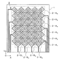
図10は、タッチパネルなどを構成する基板91上において、電極パターン92と電極パターン93とを交差させて配置する場合の電極間の接続構造の例を示す説明図である。なお、図10(a)は、接続前の電極の配置例を示す平面図である。また図10(b)は、図10(a)に示した電極の配置例のA−A’断面図である。また図10(c)は、電極を接続させた状態での接続構造の例を示す平面図である。また図10(d)は、図10(c)に示した接続構造例のA−A’断面図である。
FIG. 10 is an explanatory diagram showing an example of a connection structure between electrodes when the
図10に示す例では、基板91上に、電極パターン92と電極パターン93とを形成する場合、一方の電極パターン92を電極92aと電極92bとに分けて形成している(図10(a),(b)参照。)。そして、電極92aと電極92bを、他方の電極パターン93上の少なくとも交差領域97(図10(a)において網掛けで示す領域97)を覆うように設けられた絶縁層94を跨ぐように設けたブリッジ配線95によって接続している(図10(c),(d)参照。)。
In the example shown in FIG. 10, when the
しかし、本発明者は、このような接続構造において、電極パターン92,93およびブリッジ配線95がITOによって形成され、また絶縁層94が樹脂によって形成される場合、ITOに対して樹脂よりなる絶縁層94の密着力が弱いために、接続対象である電極92aや電極92bに被さっている箇所98,99において樹脂よりなる絶縁層94がめくれあがることによりその上層に設けられるブリッジ配線95が浮いてしまい、接続がとれなくなるという問題が生じる場合があることを見出した。
However, the present inventor has found that in such a connection structure, when the
そこで、本発明は、上記問題に鑑み、より強固に透明基板上においてある1つの透明電極を挟んで配置される2つの透明電極間を接続することができる電極間接続構造およびその電極間接続構造を利用したタッチパネルを提供することを目的とする。 Therefore, in view of the above problems, the present invention provides an interelectrode connection structure and an interelectrode connection structure capable of connecting between two transparent electrodes arranged more firmly on one transparent electrode on a transparent substrate. An object is to provide a touch panel using the.
本発明による電極間接続構造は、透明基板(例えば、透明基板1)上に透明電極として形成されるセンタ電極(例えば、図2における電極単位201cと電極単位201dと接続配線202とからなる透明電極や図4における電極202、図5における電極2B)と、センタ電極を挟んで対をなして配置される透明電極であるサイド電極(例えば、図2における電極単位201aと電極単位201bや図4における電極201、図5における電極2A)と、対をなすサイド電極を接続するための配線であるブリッジ配線(例えば、ブリッジ配線4)と、センタ電極とブリッジ配線との間に設けられる電気的絶縁層(例えば、絶縁層3)とを備え、ブリッジ配線は、金属材料からなり、電気的絶縁層は、少なくとも所定範囲内でサイド電極に接触しないように形成され、ブリッジ配線は、電気的絶縁層がサイド電極と接触しないように形成されることによりできる隙間領域で透明基板に直接接して形成されていることを特徴とする。
Between electrodes connection structure according to the invention consists of a transparent substrate (e.g., a transparent substrate 1) center electrode which is formed as a transparent electrode on (e.g., an
また、電気的絶縁層は、少なくともブリッジ配線が形成される領域内でサイド電極と接触しないように形成される。 The electrical insulating layer is formed so as not to contact the side electrode at least in a region where the bridge wiring is formed.
また、本発明による電極間接続構造は、透明基板上に透明電極として形成されるセンタ電極と、センタ電極を挟んで対をなして配置される透明電極であるサイド電極と、対をなすサイド電極を接続するための配線であるブリッジ配線と、センタ電極とブリッジ配線との間に設けられた電気的絶縁層とを備え、ブリッジ配線は、金属材料からなり、センタ電極を挟んで対をなすサイド電極を接続するブリッジ配線はセンタ電極の両側において透明基板に直接接する領域を有していることを特徴とする。 In addition, the interelectrode connection structure according to the present invention includes a center electrode formed as a transparent electrode on a transparent substrate, a side electrode that is a transparent electrode disposed in pairs with the center electrode interposed therebetween, and a pair of side electrodes. A bridge wiring that is a wiring for connecting the center electrode and an electrical insulating layer provided between the center electrode and the bridge wiring, and the bridge wiring is made of a metal material and forms a pair with the center electrode interposed therebetween. The bridge wiring connecting the electrodes has a region directly in contact with the transparent substrate on both sides of the center electrode.
また、本発明による電極間接続構造は、透明基板上に透明電極として形成されるセンタ電極と、センタ電極を挟んで対をなして配置される透明電極であるサイド電極と、センタ電極の一部を跨いで形成された電気的絶縁層と、電気的絶縁層を跨いで前記した対をなすサイド電極を接続するための配線であるブリッジ配線とを備え、ブリッジ配線は、金属材料からなり、前記したセンタ電極を跨いで形成された電気的絶縁層の両側の端部が、前記した対をなすサイド電極まで到らず、サイド電極と接触しないように形成された隙間領域を有し、当該隙間領域においてブリッジ配線が透明電極に直接接していることを特徴とする。 In addition, the interelectrode connection structure according to the present invention includes a center electrode formed as a transparent electrode on a transparent substrate, a side electrode that is a transparent electrode disposed in pairs with the center electrode interposed therebetween, and a part of the center electrode. An electrical insulating layer formed across the bridge, and a bridge wiring that is a wiring for connecting the pair of side electrodes across the electrical insulating layer, the bridge wiring is made of a metal material, A gap region formed so that the end portions on both sides of the electrically insulating layer formed across the center electrode do not reach the paired side electrodes and do not contact the side electrodes, In the region, the bridge wiring is in direct contact with the transparent electrode.
また、電気的絶縁層は、樹脂材料からなることが好ましい。 The electrical insulating layer is preferably made of a resin material.
また、本発明によるタッチパネルは、透明基板上に透明電極として形成されるセンタ電極と、センタ電極を挟んで対をなして配置されるサイド電極とを備えたタッチパネルであって、対をなすサイド電極をセンタ電極とは非導通のまま接続することによって、透明基板の片側の面において交差する列電極を形成するタッチパネルにおいて、対をなすサイド電極を接続するための配線であるブリッジ配線と、センタ電極とブリッジ配線との間に設けられる電気的絶縁層とを備え、ブリッジ配線は、金属材料からなり、電気的絶縁層は、少なくとも所定範囲内でサイド電極に接触しないように形成され、ブリッジ配線は、電気的絶縁層がサイド電極と接触しないように形成されることによりできる隙間領域で透明基板に直接接して形成されていることを特徴とする。 The touch panel according to the present invention is a touch panel including a center electrode formed as a transparent electrode on a transparent substrate and side electrodes arranged in pairs with the center electrode interposed therebetween, and the pair of side electrodes Is connected to the center electrode in a non-conducting manner to form a column electrode that intersects on one surface of the transparent substrate, and a bridge wiring that is a wiring for connecting a pair of side electrodes, and a center electrode And an electrical insulating layer provided between the bridge wiring and the bridge wiring, the bridge wiring is made of a metal material, and the electrical insulating layer is formed so as not to contact the side electrode at least within a predetermined range. The insulating layer is formed so as not to come into contact with the side electrode, and is formed in direct contact with the transparent substrate in a gap region that can be formed. And wherein the door.
また、本発明によるタッチパネルは、透明基板上に透明電極として形成されるセンタ電極と、センタ電極を挟んで対をなして配置される透明電極であるサイド電極とを備えたタッチパネルであって、対をなすサイド電極をセンタ電極とは非導通のまま接続することによって、透明基板の片側の面で交差する列電極を形成するタッチパネルにおいて、対をなすサイド電極を接続するための配線であるブリッジ配線と、センタ電極とブリッジ配線との間に設けられた電気的絶縁層とを備え、ブリッジ配線は、金属材料からなり、センタ電極を挟んで対をなすサイド電極を接続するブリッジ配線はセンタ電極の両側において透明基板に直接接する領域を有していることを特徴とする。 A touch panel according to the present invention is a touch panel including a center electrode formed as a transparent electrode on a transparent substrate, and side electrodes that are transparent electrodes arranged in pairs with the center electrode interposed therebetween. Bridge wiring that connects the pair of side electrodes in a touch panel that forms column electrodes that intersect on one side of the transparent substrate by connecting the side electrodes that form a non-conductive state with the center electrode And an electrically insulating layer provided between the center electrode and the bridge wiring, the bridge wiring is made of a metal material, and the bridge wiring for connecting the pair of side electrodes sandwiching the center electrode is connected to the center electrode. It has the area | region which touches a transparent substrate directly on both sides.
また、本発明によるタッチパネルは、透明基板上に透明電極として形成されるセンタ電極と、センタ電極を挟んで対をなして配置される透明電極であるサイド電極とを備えたタッチパネルであって、対をなすサイド電極をセンタ電極とは非導通のまま接続することによって、透明基板の片側の面で交差する列電極を形成するタッチパネルにおいて、センタ電極の一部を跨いで形成された電気的絶縁層と、電気的絶縁層を跨いで前記した対をなすサイド電極を接続するための配線であるブリッジ配線とを備え、ブリッジ配線は、金属材料からなり、前記したセンタ電極を跨いで形成された電気的絶縁層の両側の端部が、前記した対をなすサイド電極まで到らず、サイド電極と接触しないように形成された隙間領域を有し、当該隙間領域においてブリッジ配線が透明電極に直接接していることを特徴とする。 A touch panel according to the present invention is a touch panel including a center electrode formed as a transparent electrode on a transparent substrate, and side electrodes that are transparent electrodes arranged in pairs with the center electrode interposed therebetween. In a touch panel that forms a column electrode that intersects on one side of the transparent substrate by connecting the side electrode that forms a non-conductive state with the center electrode, an electrically insulating layer formed across a portion of the center electrode And a bridge wiring that is a wiring for connecting the pair of side electrodes across the electrical insulating layer, and the bridge wiring is made of a metal material and is formed by straddling the center electrode. The end portions on both sides of the mechanical insulating layer do not reach the paired side electrodes, and have gap regions formed so as not to contact the side electrodes. Wherein the ridge lines are in direct contact with the transparent electrode.
本発明によれば、より強固に透明基板上においてある1つの透明電極を挟んで配置される2つの透明電極間を接続することができる。 ADVANTAGE OF THE INVENTION According to this invention, between the 2 transparent electrodes arrange | positioned on both sides of one transparent electrode on a transparent substrate can be connected more firmly.
以下、本発明の実施形態を図面を参照して説明する。図1は、本実施形態のタッチパネルの構成例を示す説明図である。図1に示すタッチパネル10は、本発明による電極間接続構造を備えたタッチパネルである。なお、図1(a)は、タッチパネル10の平面図である。また、図1(b)は、タッチパネル10の断面図(A−A’断面図)である。なお、図1(a)ではタッチパネル10を裏側から見た場合の平面図を示し、図1(b)ではタッチパネル10の裏側を上にした断面図を示している。
Hereinafter, embodiments of the present invention will be described with reference to the drawings. FIG. 1 is an explanatory diagram illustrating a configuration example of a touch panel according to the present embodiment. A
図1に示すタッチパネル10は、ガラス基板等の透明基板1の片側の面に、交差するX軸、Y軸の2軸それぞれの軸方向に伸びる列電極が、その交差部分において間に電気的絶縁層を介することにより電気的に非接触状態で形成されることにより構成されている。ここにおいて、X軸方向に伸びる列電極をサイド電極、Y軸方向に伸びる列電極をセンタ電極と呼び、以下、説明する。なお、タッチパネルの方向の見方によって、X軸方向に伸びる列電極をセンタ電極、Y軸方向に伸びる列電極をサイド電極と読み代えることもできる。タッチ位置を検出するためには、各軸方向に伸びるサイド電極とセンタ電極とが互いに独立していなければならない。このため、本実施形態では、透明基板1の片側の面に、マトリックス状を構成する各々のサイド電極とセンタ電極の列電極パターン(各軸方向に伸びる複数列の電極パターン)を1層の透明電極パターンとして配列させた上で、2つの列が交差する領域においていずれか一方の列を他方の列と接触しないよう分断させた形で形成される透明電極パターン2と、透明電極パターン2の分断箇所を接続させるための個々のブリッジ配線4とを形成する。なお、ブリッジ配線4と透明電極パターン2とが重なり合う領域(交差領域)においては、透明電極パターン2とブリッジ配線4との間に絶縁性物質による絶縁層3を設けられている。このようにして、透明基板1の片側の面に、マトリックス状に配置されるX軸方向のサイド電極とY軸方向のセンタ電極を形成する。以下、サイド電極、センタ電極と表現した場合には、ブリッジ配線4を介する等により各電極がその各電極が並ぶ軸方向において電気的に接続がされた状態を指す場合がある。
In the
図2および図3に、透明電極パターン2の配置例を示す。図1に示した透明電極パターン2は、図2に局所的に示すように、交差する2軸をX軸とY軸とした場合に、少なくともX軸方向に沿って列をなす2以上の電極単位201(例えば、電極単位201a,201b)とY軸方向に沿って列をなす2以上の電極単位201(例えば、電極単位201c,201d)とを含む電極単位集合と、X軸方向とY軸方向とで交差する位置関係で配置されている各電極単位(図2に示す例では、電極単位201a,201bと電極単位201c,201d)をいずれか一方の軸方向でのみ接続させる接続配線202とにより構成されている。例えば、図2に示す電極単位201a,201bは、図3における列電極パターン2−A1を構成する一構成要素に相当する。また、例えば、図2に示す電極単位201c,201dは、図3における列電極パターン2−B4を構成する一構成要素に相当する。なお、図2に示す例では、各列をなす電極集合への引き廻し配線203(例えば、引き廻し配線203a,203b)も示している。引き廻し配線203は、各列電極パターンを構成する電極単位201のいずれか1つに接続されていればよい。
2 and 3 show examples of arrangement of the
なお、列電極パターンは、電極単位201や接続配線202を区別せずにひとつなぎの電極として形成することも可能である。例えば、図2に示す例では、電極単位201cと電極単位201dと接続配線202とを区別せずに1つの透明電極として形成することも可能である。この場合、図2に示す例では、1つの透明電極(ここでは、電極単位201cと電極単位201dと接続配線202とによって構成される透明電極)と、該透明電極を間に挟むように隔置されて配置される2つの透明電極(ここでは、電極単位201aと電極単位201b)の3つの独立した透明電極が形成されていると表現することも可能である。
Note that the column electrode pattern can be formed as a single electrode without distinguishing the
本実施形態では、図3に示すように、各軸方向に沿って列をなす一連の電極単位201集合を、電極単位201間が接続配線202により接続されるか否かに関わらず、1つの列電極パターンとして扱う。透明電極パターン2を形成した時点で電極単位間が接続されていなくても、最終的にブリッジ配線4(図1参照。)により接続されるからである。図3に示す例では、10個の列電極パターン2−A1〜2−A6、2−B1〜2−B4が形成されていると表現できる。
In the present embodiment, as shown in FIG. 3, a series of
図3には、X軸方向に沿って列をなすサイド電極の列電極パターンとして、Y軸座標を検出するための6列の列電極パターン2−A1〜2−A6が形成される例が示されている。また、Y軸方向に沿って列をなすセンタ電極の列電極パターンとして、X軸座標を検出するための4列の列電極パターン2−B1〜2−B4が形成される例が示されている。 FIG. 3 shows an example in which six columns of column electrode patterns 2-A 1 to 2-A 6 for detecting Y-axis coordinates are formed as the column electrode patterns of the side electrodes that form columns along the X-axis direction. It is shown. In addition, an example is shown in which four column electrode patterns 2-B 1 to 2-B 4 for detecting the X-axis coordinates are formed as the column electrode patterns of the center electrodes that form columns along the Y-axis direction. ing.
各電極単位201は、その形状に応じてそれぞれが平面的に隔置、分離され、かつ隙間が少なくなるように配置され、タッチパネルとして任意の精度が得られるようにされていればよい。例えば、X軸方向に列をなす電極単位201とY軸方向に列をなす電極単位201とが密にタッチ領域全体に配置されるように、かつ各軸方向の列電極パターン2が交差する領域が可能な限り小さい領域ですむように、矩形やひし形、六角形といった多角形状で、互い違いにあるいは直列状に配列されていてもよい。また、電極単位は、その形状内に、切り込みや穴が設けられていてもよい。このようにすることで、使用者に電極単位を視認されにくくすることができる。
Each
透明基板1は、電気絶縁性の基板であって、例えば、ガラス基板や、PET(ポリエチレンテレフタレート)フィルム/シート、PC(ポリカードネート)フィルム/シートなどでよい。
The
また、絶縁層3を構成する透明性の電気絶縁性物質として、例えば、SiO2などの無機材料やフォトリソ樹脂などの有機樹脂材料を用いることが可能である。しかし、前者のSiO2の場合には、スパッタリング法によりマスクを利用してパターニングされた絶縁層を容易に得ることができるが、マスクを使用してスパッタリング法により無機材料の膜を形成する場合、位置精度が悪く、ブリッジ配線を長くする必要が生じる。そのため、この電気的絶縁層は、位置精度が高いフォトリソ樹脂材料を用いて形成された樹脂層が好ましい。フォトリソ樹脂を使用して絶縁層を形成する場合には、フォトリソプロセスにより容易にパターニングされた樹脂製の絶縁層を得ることができる。
Further, as the transparent electrical insulating substance constituting the insulating
特に、透明基板がガラス基板の場合には、ガラス基板の表面に生ずるシラノール基と反応する基を有するフォトリソ樹脂(感光性樹脂)が好ましい。かかる感光性樹脂を使用することにより、ガラス基板と感光性樹脂との間で化学結合が生じて密着力の高い絶縁層を形成することができる。例えば、感光性アクリル系樹脂、感光性メタクリル系樹脂、感光性ポリイミ系樹脂、感光性ポリシロキサン系樹脂、感光性ポリビニールアルコール樹脂、アクリルウレタン系感光性樹脂などが挙げられる。 In particular, when the transparent substrate is a glass substrate, a photolitho resin (photosensitive resin) having a group that reacts with a silanol group generated on the surface of the glass substrate is preferable. By using such a photosensitive resin, a chemical bond is generated between the glass substrate and the photosensitive resin, so that an insulating layer having high adhesion can be formed. For example, a photosensitive acrylic resin, a photosensitive methacrylic resin, a photosensitive polyimid resin, a photosensitive polysiloxane resin, a photosensitive polyvinyl alcohol resin, an acrylic urethane photosensitive resin, and the like can be given.
また、ブリッジ配線4を構成する導電物質としては、透明基板1に対して高い密着力を容易に得ることができる金属材料が望ましく使用される。特に、透明基板がガラス基板の場合には、ガラス基板に対して密着力が高く、ITOより導電性が高く、耐久性、耐摩耗性にも優れた、Mo、Mo合金、Al、Al合金、Au、Au合金などの金属材料を好ましく用いることができる。より耐食性を高めた合金としては、例えば、Mo−Nb系合金、Al−Nd系合金などが好ましい例として挙げられる。上記のようなブリッジ配線は2層、3層などの多層構造としてもよい。例えば、Mo層/Al層/Mo層の3層構造が挙げられる。かかる金属材料からなるブリッジ配線は、ITOを使用する場合に比べ、配線幅を細く、また短く、また層厚を薄くすることができ、設計の自由度を高め、また外観を良くすることができる。
Further, as the conductive material constituting the
図4は、透明基板1に透明電極パターン2と絶縁層3とブリッジ配線4とが積層された状態を拡大して示す説明図である。なお、図4は、サイド電極の列電極パターン2−A1とセンタ電極の列電極パターン2−B1とが交差する領域を、X軸方向に沿った断面図を示している。図4に示す例では、列電極パターン2−A1と列電極パターン2−B1とが交差する領域では、透明電極パターン2として列電極パターン2−A1が分断された形(分断形状)で形成され、代わりに列電極パターン2−B1が分断させれない形(接続形状)で形成されている。そして、接続形状で形成された列電極パターン2−B1のうち列電極パターン2−A1との交差領域にあたる部位(以下、交差部位という。例えば、図2における接続配線202の一部分)を覆うように絶縁層3が形成され、その絶縁層3を跨いで分断されている列電極パターン2−A1(例えば、列電極パターン2−A1を構成する一列に並んだ2つの電極単位201)を接続させるブリッジ配線4が形成されている。
FIG. 4 is an explanatory view showing, in an enlarged manner, a state in which the
本実施形態において、絶縁層3は、ブリッジ配線4による接続対象である2つの電極単位(図4においてサイド電極の列電極パターン2−A1として形成される2つの電極210。)それぞれと接触しないように形成されるものとする。また、ブリッジ配線4が2つのサイド電極210を接続した状態において、絶縁層3と各サイド電極210との間に、ブリッジ配線4が透明基板1に直接接する部位である密着部位41が含まれるようにブリッジ配線4を形成する。各密着部位41は、例えば、絶縁層3と各サイド電極210の電極単位との間の隙間領域の長さ方向(図においてX軸方向)に対して全体に渡るように形成することがブリッジ配線をより強固に透明電極に固着させる上で好ましいが、隙間領域の長さ方向に対して所定部分、例えば、隙間領域の長さに対して略半分以上の長さ程度で設けてもよい。図4において、2つのサイド電極210に対して、そのサイド電極210に挟まれて配置される電極(図4において列電極パターン2−B1として形成される電極)はセンタ電極220である。
In this embodiment, the insulating
また、図5は、透明電極パターン2と絶縁層3とブリッジ配線4の他の配置例を示す説明図である。図5に示す例では、透明電極パターン2として、1つのセンタ電極2Bと、センタ電極2Bを挟むように配置される2つのサイド電極2Aとが形成されている。図5に示すように、絶縁層3は、少なくともブリッジ配線4が跨る領域において、各サイド電極2Aと接しないように形成されていればよい。例えば、絶縁層3は、ブリッジ配線4が形成される領域以外の領域(例えば、領域301,302,303,304)において、サイド電極2Aと接していてもよいし、また、サイド電極2Aの上に載るような形状であってもよい。
FIG. 5 is an explanatory diagram showing another arrangement example of the
図5に示す例では、絶縁層3のX軸方向の幅は、ブリッジ配線4と重なる領域では狭くなり、ブリッジ配線4と重なる領域において絶縁層3はサイド電極2Aと接触していない。また、ブリッジ配線4と重なっていない領域では、絶縁層3のX軸方向の幅が広がり、絶縁層3は、領域301〜304においてサイド電極2Aと接する。このように、絶縁層3のうち、ブリッジ電極4と重なっていな井部分は、サイド電極と接していてもよい。
In the example shown in FIG. 5, the width of the insulating
これにより、少なくともブリッジ配線4が形成される領域内では、絶縁層3が接続対象である各サイド電極210の上に載る形状とはならないので、絶縁層3のはがれ現象によりブリッジ配線4の接続がとれなくなるといった接続状態の劣化現象の発生を防止することができる。これは、透明電極がガラス基板の場合、樹脂層(絶縁層3)と透明基板1との密着力と、樹脂層(絶縁層3)とITOとの密着力とを比較した場合に、その表面にOH基を有している透明基板1の方が樹脂層との間に化学結合を生じさせることができるために密着力が高いことを利用したものである。これによって、絶縁層3のはがれ現象によりブリッジ配線4の接続がとれなくなるといった接続状態の劣化現象の発生を防止することができる。さらに、金属材料を選択してブリッジ配線4を形成することによって、ITO等の金属酸化膜により形成する場合と比べて、ブリッジ配線4自体の透明基板1に対する密着力をより高めることができる。このように、絶縁層3とサイド電極の電極単位との間の隙間領域において、絶縁層3と透明基板1との密着力だけでなくブリッジ配線4と透明基板1との密着力をも利用して、より強度にブリッジ配線4と各透明電極とを接続させることができる。
Accordingly, at least in the region where the
次に、本実施形態のタッチパネル10の製造方法の一例について説明する。まず、透明基板1の片側の面に、透明電極パターン2を形成する。例えば、透明基板1の片側の面に、スパッタリング法などを用いてITOを成膜させ、成膜させたITO膜をフォトリソグラフィ技術などを利用して図3に示すようなパターン形状に加工することにより、所定パターンを有する透明電極パターン2を形成する。次に、透明電極パターン2が形成されている透明基板1の同面(透明電極パターン2が形成されている面)に、透明電極パターン2の特定部位(X軸方向のサイド電極の列電極パターンとY軸方向のセンタ電極の列電極パターンとが交差する領域。すなわち、列電極パターンとしての交差領域。)を覆う絶縁層3を形成する。この絶縁層3を形成するにあたっては、フォトリソ樹脂をコーティングし、所定パターンのマスクを用いて露光し、ついでエッチングするというフォトリソグラフィー・プロセス法を採用する。この際、上記の交差領域において、絶縁層の両側の端部が、その両側のサイド電極まで到らず、サイド電極と接触していない隙間領域が形成されるようにする。図6は、各交差領域に絶縁層3が形成された状態のタッチパネル10の例を示す説明図である。
Next, an example of the manufacturing method of the
次に、各交差領域に設けた絶縁層3の上を跨ぐようにして透明電極パターン2の特定部位(サイド電極の列電極パターン2において分断して形成した電極単位の一部)間を接続させる各ブリッジ配線4を形成する。例えば、絶縁層3が形成されている透明基板1の同面(絶縁層3が形成されている面)に対してスパッタリング法などを用いて金属製の導電物質を成膜して金属膜を形成し、この金属膜をフォトリソグラフィ法によりパターニングして所定形状のパターンを有するブリッジ配線4を形成する。これにより、図1に示す状態が完成する。
Next, a specific part of the transparent electrode pattern 2 (a part of the electrode unit divided and formed in the
上記した各列の電極パターンの引き廻し配線の低抵抗化が要求される場合には、ブリッジ配線を形成する工程において絶縁層が形成されている透明基板の同面に対してスパッタリング法などを用いて金属膜を形成する際、引き廻し配線部分も覆って金属膜を形成し、この金属膜をブリッジ配線の形成のためのフォトリソグラフィ法によるパターニング工程と同時にパターニングを行って引き廻し配線上に低抵抗の金属膜を形成するようにしてもよい。 When it is required to reduce the resistance of the wiring pattern of the electrode pattern in each row, a sputtering method or the like is used for the same surface of the transparent substrate on which the insulating layer is formed in the step of forming the bridge wiring. When the metal film is formed, the metal film is also formed so as to cover the routing wiring portion, and this metal film is patterned simultaneously with the patterning process by the photolithography method for forming the bridge wiring to reduce the thickness on the routing wiring. A resistive metal film may be formed.
また、各列の電極パターンの引き廻し配線が、予め形成されていない場合には、ブリッジ配線を形成する工程において絶縁層が形成されている透明基板の同面に対してスパッタリング法などを用いて金属膜を形成する際、形成しようとする引き廻し配線部分も覆って金属膜を形成し、この金属膜をブリッジ配線の形成のためのフォトリソグラフィ法によるパターニング工程と同時にパターニングを行って引き廻し配線を上記金属膜によって形成するようにしてもよい。 In addition, when the wiring pattern of the electrode pattern in each column is not formed in advance, a sputtering method or the like is used for the same surface of the transparent substrate on which the insulating layer is formed in the step of forming the bridge wiring. When forming a metal film, a metal film is also formed covering a portion of the routing wiring to be formed, and this metal film is patterned simultaneously with a patterning process by a photolithography method for forming a bridge wiring, and the routing wiring is formed. May be formed of the metal film.
なお、図1に示す例では、最初に透明電極パターン2を形成し、その次に絶縁層3を形成し、次いでブリッジ配線4を形成する例を示しているが、この順番は逆であってもよい。すなわち、最初に交差領域となる部分に各ブリッジ配線4を形成し、その次に各ブリッジ配線401の中間部(少なくとも透明電極パターン2の交差部位が形成される領域を含む)を覆いつつ両端部が露出するように絶縁層3を形成し、次いで、透明電極パターン2を、各ブリッジ配線4の両端部が、当該ブリッジ配線4の接続対象である2つの電極単位と接続されることにより当該電極単位間が導通状態となるように形成してもよい。このような順においても、各絶縁層3を、当該絶縁層3が覆うブリッジ配線4の接続対象である2つの電極単位と接しないように形成する。なお、本実施形態では、交差領域に位置する一方の列電極パターンを構成する透明電極との間に絶縁層3を挟み込んだ状態で、他方の列電極パターンを構成する分断された透明電極を接続する配線であれば、絶縁層3の上を跨ぐように形成されるか又は下を潜るように形成されるかに関わらず、ブリッジ配線4と呼ぶこととする。
In the example shown in FIG. 1, the
また、図1〜図6では、交差するサイド電極とセンタ電極の各列電極パターン2に対して、一方の軸方向の列電極パターンを分断形状とし、他方の軸方向の列電極パターンを接続形状とする例を示したが、本発明による電極間接続構造が適用される電極パターンの配置としては、独立した3つの電極が形成されていればよい。また、タッチパネルにおける列電極パターンの配置としても、図3に示した例に限らない。例えば、同じ軸方向の列電極パターンに対してある列電極パターンは接続形状とし、またある列電極パターンは分断形状とするといったパターニングも可能である。また、例えば、1つの列電極パターンにおいて、ある電極単位間は接続形状として、ある電極単位間は分断形状とするパターニングも可能である。
1 to 6, for each
また、構成の例を示す図面で図示省略しているが、タッチパネル10は、透明電極パターン2の各列電極パターンを介して静電容量を監視する回路部を備えている。この回路部は、例えば、各列の電極パターンの引き廻し配線203の端子部とフレキシブルフィルム等を介して接続されていればよい。なお、各列の電極パターンの引き廻し配線203の端子部と接続されるフレキシブルフィルムに直接ICチップを搭載して回路部を構成してもよい。
Although not shown in the drawing showing an example of the configuration, the
また、例えば、図8に示すように、タッチパネル10は、透明基板1上に形成される列電極(より具体的には、絶縁層3を間に挟み込んで積層される透明電極パターン2とブリッジ配線4とにより構成されるX軸方向およびY軸方向の列電極)の上に、UV硬化性樹脂等による接着層5を介して積層される保護ガラス6を設けてもよい。図8は、タッチパネル10の他の構成例を示す模式的断面図である。なお、このような構成にした場合には、保護ガラス6側からのタッチ位置を検出することも可能である。
For example, as shown in FIG. 8, the
また、例えば、図9に示すように、タッチパネル10を液晶表示装置等の表示装置に組み込み、タッチ位置が検出可能な静電容量型タッチパネル機能付表示装置として構成することも可能である。図9は、静電容量型タッチパネル機能付表示装置の構成例を示す模式的断面図である。図9に示す静電容量型タッチパネル機能付表示装置100は、タッチパネル構成部10と、表示パネル構成部20と、バックライト31とを備える。
Further, for example, as shown in FIG. 9, the
タッチパネル構成部10は、図1に示すようなタッチパネル10と同様の構成でよい。すなわち、透明基板1の片側の面に、マトリックス状に配置される透明電極パターンとして機能する列電極(より具体的には、絶縁層3を間に挟み込んで積層される透明電極パターン2とブリッジ配線4とにより構成されるX軸方向およびY軸方向の列電極)が形成されていればよい。
The touch
また、表示パネル構成部20は、一般的な表示装置と同様でよい。例えば、液晶表示装置であれば、第1の透明基板21と第2の透明基板22との間に液晶23を挟持する構成となっていてもよい。なお、符号24,25は、偏光板を示している。また、符号26は、駆動ICを示している。
Further, the display
なお、各透明基板21,22には、液晶の状態を制御するためにセグメント電極やコモン電極などが形成されるが、これらの電極の図示は省略している。また、液晶23は、各透明基板21,22およびシール材によって封止されるが、シール材の図示は省略している。
Each
例えば、タッチパネル構成部10の透明基板1上に形成される列電極と、表示パネル構成部20の視認側の最上位層(ここでは、偏光板24)とをUV硬化性樹脂等による接着層5を介して重ね合わせることにより、1つの液晶表示装置として構成することが可能である。図9に示す例では、タッチパネルを構成する透明基板1の列電極が形成される面を液晶表示装置側として重ね合わせる例を示している。このように、タッチ位置を検出するための列電極が透明基板1の片側の面だけに形成されているため、保護ガラスといった部品点数を増やすことなく、容易に表示装置に組み込むことができる。また、表示内容をタッチ状況により変更させるなどの表示装置との連携により、タッチパネルの押す場所をわかりやすくすることもできる。
For example, the column electrode formed on the
なお、液晶表示装置と重ね合わせることによって、タッチパネル構成部10の透明基板1に形成される各列電極パターンから検出される静電容量の変化にノイズが発生してしまう場合には、タッチパネル構成部10と表示パネル構成部20との間に、アースとして機能させる透明電極を設けてもよい。タッチパネル構成部10と表示パネル構成部20との間に設ける透明電極は、パターニングせずにパネル領域の面全体を覆うように形成すればよい。
In addition, when noise is generated in the change in capacitance detected from each column electrode pattern formed on the
なお、アースとして機能させる透明電極は、タッチパネル構成部10の透明基板1に形成される列電極から見て、タッチされる側とは反対の側に位置するように形成されていればよい。例えば、タッチパネル構成部10を、図8に示すように、透明基板1に形成される列電極に対して樹脂等による接着層5を介して保護ガラス6を積層する構成にし、液晶表示パネル構成部20の最上層と重ね合わせる側の基板面全体にITO等による透明電極を形成した上で、再度UV硬化性樹脂等による接着層5を介して重ね合わせてもよい。このような構成にすれば、表示装置からのノイズの影響を受けずに安定して、タッチ位置を検出することが可能である。
Note that the transparent electrode that functions as the ground may be formed so as to be positioned on the side opposite to the touched side as viewed from the column electrode formed on the
なお、タッチ位置を検出するための列電極が形成される透明基板1に対して、表示装置や保護ガラス(保護カバー)などを積層する方法として、UV硬化性樹脂等を用いる例を示したが、この他にも、両面接着フィルム(PSA)を用いる方法がある。PSAを用いる場合には、例えば、列電極の上にPSAを貼り付け、その後真空中で液晶表示装置や保護カバーと重ねあわせを実施すればよい。その後、オートクレーブ装置(加圧脱泡装置)等を用いて泡をなくしつつ加圧させることが好ましい。また、樹脂を用いる場合には、透明基板上の列電極の上に、液体状の樹脂を塗布し、液晶表示装置や保護カバーをゆっくり積層させ、最後にUV露光を行って樹脂を硬化させればよい。
In addition, although the example using UV curable resin etc. was shown as a method of laminating | stacking a display apparatus, protective glass (protective cover), etc. with respect to the
本実施例は、横4cm×縦6cmのタッチ領域を得るために4列のセンタ電極の列電極パターンと6列のサイド電極の列電極パターンをマトリックス状に配置させるタッチパネルの例である。本実施例では、0.55mmのガラス基板の片側の面に、膜厚20nmのITO膜をスパッタリング法により成膜し、これをフォトリソグラフィ技術を利用して、図3に示すパターン形状に加工し、各電極パターン2を形成した。すなわち、各列電極パターンを構成する電極単位201の形状をひし形とし、横方向であるX軸方向に列をなす電極単位集合により構成される6列のサイド電極の列電極パターン2−A1〜2−A6と、縦方向であるY軸方向に列をなす電極単位集合により構成される4列のセンタ電極の列電極パターン2−B1〜2−B4と、それらへの引き廻し配線とを含む透明電極パターン2を形成した。なお、本実施形態では、各列電極パターンうち、Y軸方向に列をなす電極集合により構成されるセンタ電極の列電極パターン2−B1〜2−B4については各電極を接続する接続配線202を設けて接続形状とし、一方のサイド電極の列電極パターン2−A1〜2−A6については接続配線202を設けずに各電極が分断される分断形状としている。また、本例では、ひし形の電極単位201の一辺の長さを5mm、接続配線202の幅を0.5mm、接続配線202の長さを1.5mmとしている。
This embodiment is an example of a touch panel in which a column electrode pattern of 4 columns of center electrodes and a column electrode pattern of 6 columns of side electrodes are arranged in a matrix in order to obtain a touch area of 4 cm wide × 6 cm long. In this embodiment, an ITO film having a thickness of 20 nm is formed on one surface of a 0.55 mm glass substrate by a sputtering method, and this is processed into a pattern shape shown in FIG. 3 using a photolithography technique. Each
次に、上記透明電極パターンを覆ってアクリル樹脂系のフォトリソ樹脂を塗布し、このフォトリソ樹脂の塗膜を所定のパターンを有する露光マスクを用いたフォトリソグラフィ技術を利用して、サイド電極の列電極パターン2−A1〜2−A6とセンタ電極の列電極パターン2−B1〜2−B4とが交差する領域において接続形状で形成されたセンタ電極の列電極パターン2−B1〜2−B4を跨ぎ、しかしその両側のサイド電極の列電極パターン2−A1〜2−A6まで達せず、隙間領域が形成されるようなパターンをもって、樹脂製の電気的絶縁層を形成する。このようにすることにより、絶縁層の両側の端部は、サイド電極まで到らないような構造となる。この絶縁層のそれぞれはX軸方向の長さは1.0mmで、Y軸方向の長さ(幅)は1.5mmになるようにした。この厚みは1.8μmとした。
Next, an acrylic resin-based photolitho resin is applied so as to cover the transparent electrode pattern, and this photolitho resin coating film is applied to the column electrode of the side electrode using a photolithographic technique using an exposure mask having a predetermined pattern.
次に、上記透明電極パターンおよび絶縁層を覆って導電性の金属膜をスパッタリング法により膜厚が350nmとなるように成膜し、所定のパターンを有する露光マスクを用いたフォトリソグラフィ技術を利用してブリッジ配線を形成した。本実施例では、金属膜としては金属層の3層構造とし、ガラス基板側より、Nb含有のMo層、Nd含有のAl層、Nb含有のMo層の3層を使用し、またブリッジ配線のX軸方向の長さは5.0mmとし、その幅は0.1mmとし、その膜厚は20μmとした。 Next, a conductive metal film is formed by sputtering to cover the transparent electrode pattern and the insulating layer so as to have a film thickness of 350 nm, and a photolithography technique using an exposure mask having a predetermined pattern is used. The bridge wiring was formed. In this embodiment, the metal film has a three-layer structure of metal layers, and uses three layers of an Nb-containing Mo layer, an Nd-containing Al layer, and an Nb-containing Mo layer from the glass substrate side. The length in the X-axis direction was 5.0 mm, the width was 0.1 mm, and the film thickness was 20 μm.
このようにして図7に示すように、センタ電極の列電極パターンの電極単位201cおよび201dの接続配線202を跨いで樹脂製の電気的絶縁層3を形成し、接続配線202とその両側のサイド電極の列電極パターンの電極単位201aおよび201bとの間に隙間領域pが形成される。また、電気的絶縁層3を跨いでサイド電極の列電極パターンの電極単位201aおよび201bを接続するブリッジ配線4が形成される。ここにおいて、ブリッジ配線4は、隙間間隔pにおいて透明基板の表面と直接接している。
In this way, as shown in FIG. 7, the resin-made electrically insulating
そして、透明基板1上に形成される各列電極パターンの引き廻し配線203の端子部に、回路基板をフレキシブルフィルムを介して接続した。このようにして完成したタッチパネル10で、指で触った場所を感知できることを確認した。また、このようにして完成したタッチパネル10に対して、さらに、樹脂による接着層5を介して保護ガラス6を積層しても、指で触った場所を感知できることを確認した。
And the circuit board was connected to the terminal part of the
本発明は、マトリックス方式を利用してタッチ位置を検出するタッチパネルにを構成する透明基板上の透明電極間の接続だけでなく、基板上である電極に対して電気的に導通させずに当該電極を跨いで他の2つの電極を接続させたい場合においても好適に適用可能である。 The present invention provides not only a connection between transparent electrodes on a transparent substrate that constitutes a touch panel that detects a touch position using a matrix system, but also the electrodes without being electrically connected to the electrodes on the substrate. The present invention can also be suitably applied when it is desired to connect the other two electrodes across the two.
10 タッチパネル,タッチパネル構成部
1 透明基板
2 透明電極パターン
2−A1〜2−A6、2−B1〜2−B4 各列電極パターン
201 電極単位
202 接続配線
203 引き廻し配線
210 サイド電極
220 センタ電極
3 絶縁層
4 ブリッジ配線
41 密着部位
5 接着層
6 保護ガラス(保護カバー)
7 絶縁層3用マスクパターン
8 ブリッジ配線4用マスクパターン
9 透明電極パターン2用マスクパターン
100 静電容量型タッチパネル機能付表示装置
20 表示パネル構成部
21 第1の透明基板
22 第2の透明基板
23 液晶
24 偏光板
25 偏光板
26 駆動IC
31 バックライト
10 touch panel, the transparent electrode pattern touch
7 Mask Pattern for Insulating
31 Backlight
Claims (10)
前記センタ電極を挟んで対をなして配置される透明電極であるサイド電極と、
対をなす前記サイド電極を接続するための配線であるブリッジ配線と、
前記センタ電極と前記ブリッジ配線との間に設けられる電気的絶縁層とを備え、
前記ブリッジ配線は、金属材料からなり、
前記電気的絶縁層は、少なくとも所定範囲内で前記サイド電極に接触しないように形成され、
前記ブリッジ配線は、前記電気的絶縁層が前記サイド電極と接触しないように形成されることによりできる隙間領域で前記透明基板に直接接して形成されている
ことを特徴とする電極間接続構造。 A center electrode formed as a transparent electrode on a transparent substrate;
Side electrodes that are transparent electrodes arranged in pairs with the center electrode in between;
A bridge wiring that is a wiring for connecting the pair of side electrodes;
An electrical insulating layer provided between the center electrode and the bridge wiring;
The bridge wiring is made of a metal material,
The electrical insulating layer is formed so as not to contact the side electrode at least within a predetermined range,
The inter-electrode connection structure, wherein the bridge wiring is formed in direct contact with the transparent substrate in a gap region formed by forming the electrical insulating layer so as not to contact the side electrode.
請求項1に記載の電極間接続構造。 The interelectrode connection structure according to claim 1, wherein the electrical insulating layer is formed so as not to contact the side electrode at least in a region where the bridge wiring is formed.
前記センタ電極を挟んで対をなして配置される透明電極であるサイド電極と、
対をなす前記サイド電極を接続するための配線であるブリッジ配線と、
前記センタ電極と前記ブリッジ配線との間に設けられた電気的絶縁層とを備え、
前記ブリッジ配線は、金属材料からなり、
前記センタ電極を挟んで対をなすサイド電極を接続するブリッジ配線は前記センタ電極の両側において透明基板に直接接する領域を有している
ことを特徴とする電極間接続構造。 A center electrode formed as a transparent electrode on a transparent substrate;
Side electrodes that are transparent electrodes arranged in pairs with the center electrode in between;
A bridge wiring that is a wiring for connecting the pair of side electrodes;
An electrical insulating layer provided between the center electrode and the bridge wiring;
The bridge wiring is made of a metal material,
The inter-electrode connection structure, wherein the bridge wiring connecting the pair of side electrodes sandwiching the center electrode has regions directly in contact with the transparent substrate on both sides of the center electrode.
前記センタ電極を挟んで対をなして配置される透明電極であるサイド電極と、
前記センタ電極の一部を跨いで形成された電気的絶縁層と、
前記電気的絶縁層を跨いで前記した対をなすサイド電極を接続するための配線であるブリッジ配線とを備え、
前記ブリッジ配線は、金属材料からなり、
前記したセンタ電極を跨いで形成された電気的絶縁層の両側の端部が、前記した対をなすサイド電極まで到らず、前記サイド電極と接触しないように形成された隙間領域を有し、当該隙間領域においてブリッジ配線が透明電極に直接接している
ことを特徴とする電極間接続構造。 A center electrode formed as a transparent electrode on a transparent substrate;
Side electrodes that are transparent electrodes arranged in pairs with the center electrode in between;
An electrically insulating layer formed across a portion of the center electrode;
A bridge wiring that is a wiring for connecting the pair of side electrodes across the electrical insulating layer;
The bridge wiring is made of a metal material,
Ends on both sides of the electrical insulating layer formed across the center electrode described above do not reach the paired side electrodes, and have a gap region formed so as not to contact the side electrodes, An interelectrode connection structure, wherein the bridge wiring is in direct contact with the transparent electrode in the gap region.
対をなす前記サイド電極を接続するための配線であるブリッジ配線と、
前記センタ電極と前記ブリッジ配線との間に設けられる電気的絶縁層とを備え、
前記ブリッジ配線は、金属材料からなり、
前記電気的絶縁層は、少なくとも所定範囲内で前記サイド電極に接触しないように形成され、
前記ブリッジ配線は、前記電気的絶縁層が前記サイド電極と接触しないように形成されることによりできる隙間領域で前記透明基板に直接接して形成されている
ことを特徴とするタッチパネル。 A touch panel comprising a center electrode formed as a transparent electrode on a transparent substrate and side electrodes arranged in pairs with the center electrode interposed therebetween, wherein the pair of side electrodes is the center electrode. In the touch panel that forms column electrodes that intersect on one side of the transparent substrate by connecting in a non-conductive state,
A bridge wiring that is a wiring for connecting the pair of side electrodes;
An electrical insulating layer provided between the center electrode and the bridge wiring;
The bridge wiring is made of a metal material,
The electrical insulating layer is formed so as not to contact the side electrode at least within a predetermined range,
The touch panel, wherein the bridge wiring is formed in direct contact with the transparent substrate in a gap region formed by forming the electrical insulating layer so as not to contact the side electrode.
請求項6に記載のタッチパネル。 The touch panel according to claim 6, wherein the electrical insulating layer is formed so as not to contact the side electrode at least in a region where the bridge wiring is formed.
対をなす前記サイド電極を接続するための配線であるブリッジ配線と、
前記センタ電極と前記ブリッジ配線との間に設けられた電気的絶縁層とを備え、
前記ブリッジ配線は、金属材料からなり、
前記センタ電極を挟んで対をなすサイド電極を接続するブリッジ配線は前記センタ電極の両側において透明基板に直接接する領域を有している
ことを特徴とするタッチパネル。 A touch panel comprising: a center electrode formed as a transparent electrode on a transparent substrate; and a side electrode that is a transparent electrode disposed in pairs with the center electrode interposed therebetween, wherein the side electrodes that form a pair are In the touch panel that forms column electrodes that intersect on one side of the transparent substrate by connecting with the center electrode while being non-conductive,
A bridge wiring that is a wiring for connecting the pair of side electrodes;
An electrical insulating layer provided between the center electrode and the bridge wiring;
The bridge wiring is made of a metal material,
The touch panel, wherein the bridge wiring connecting the pair of side electrodes sandwiching the center electrode has regions directly in contact with the transparent substrate on both sides of the center electrode.
前記センタ電極の一部を跨いで形成された電気的絶縁層と、
前記電気的絶縁層を跨いで前記した対をなすサイド電極を接続するための配線であるブリッジ配線とを備え、
前記ブリッジ配線は、金属材料からなり、
前記したセンタ電極を跨いで形成された電気的絶縁層の両側の端部が、前記した対をなすサイド電極まで到らず、前記サイド電極と接触しないように形成された隙間領域を有し、当該隙間領域においてブリッジ配線が透明電極に直接接している
ことを特徴とするタッチパネル。 A touch panel comprising: a center electrode formed as a transparent electrode on a transparent substrate; and a side electrode that is a transparent electrode disposed in pairs with the center electrode interposed therebetween, wherein the side electrodes that form a pair are In the touch panel that forms column electrodes that intersect on one side of the transparent substrate by connecting with the center electrode while being non-conductive,
An electrically insulating layer formed across a portion of the center electrode;
A bridge wiring that is a wiring for connecting the pair of side electrodes across the electrical insulating layer;
The bridge wiring is made of a metal material,
Ends on both sides of the electrical insulating layer formed across the center electrode described above do not reach the paired side electrodes, and have a gap region formed so as not to contact the side electrodes, A touch panel, wherein the bridge wiring is in direct contact with the transparent electrode in the gap region.
Priority Applications (3)
| Application Number | Priority Date | Filing Date | Title |
|---|---|---|---|
| JP2009121354A JP2010271796A (en) | 2009-05-19 | 2009-05-19 | Connection structure between electrodes and touch panel |
| CN201010188922.1A CN101893958B (en) | 2009-05-19 | 2010-05-18 | Connection structure between electrodes and touch panel |
| US12/782,221 US20100295819A1 (en) | 2009-05-19 | 2010-05-18 | Connection structure between electrodes and touch panel |
Applications Claiming Priority (1)
| Application Number | Priority Date | Filing Date | Title |
|---|---|---|---|
| JP2009121354A JP2010271796A (en) | 2009-05-19 | 2009-05-19 | Connection structure between electrodes and touch panel |
Publications (2)
| Publication Number | Publication Date |
|---|---|
| JP2010271796A true JP2010271796A (en) | 2010-12-02 |
| JP2010271796A5 JP2010271796A5 (en) | 2012-06-28 |
Family
ID=43103166
Family Applications (1)
| Application Number | Title | Priority Date | Filing Date |
|---|---|---|---|
| JP2009121354A Pending JP2010271796A (en) | 2009-05-19 | 2009-05-19 | Connection structure between electrodes and touch panel |
Country Status (3)
| Country | Link |
|---|---|
| US (1) | US20100295819A1 (en) |
| JP (1) | JP2010271796A (en) |
| CN (1) | CN101893958B (en) |
Cited By (11)
| Publication number | Priority date | Publication date | Assignee | Title |
|---|---|---|---|---|
| JP2011170311A (en) * | 2010-02-22 | 2011-09-01 | Samsung Mobile Display Co Ltd | Touch screen panel and fabricating method thereof |
| JP2012128605A (en) * | 2010-12-14 | 2012-07-05 | Kyocera Display Corp | Touch panel |
| KR20130061854A (en) * | 2011-12-02 | 2013-06-12 | 엘지디스플레이 주식회사 | Touch screen panel and method of fabricating the same |
| JP2013235354A (en) * | 2012-05-08 | 2013-11-21 | Kyocera Display Corp | Touch panel |
| JPWO2012090998A1 (en) * | 2010-12-28 | 2014-06-05 | 京セラ株式会社 | Display device |
| KR101427995B1 (en) | 2013-08-12 | 2014-08-08 | 동우 화인켐 주식회사 | Touch sensing electrode |
| JP2015079526A (en) * | 2011-08-12 | 2015-04-23 | 宸鴻科技(廈門)有限公司TPK Touch Solutions(Xiamen)Inc. | Capacitive touch panel, and reduction method of visibility of metal jumper on capacitive touch panel |
| KR101562487B1 (en) | 2012-02-10 | 2015-10-21 | 알프스 덴키 가부시키가이샤 | Input device |
| KR20160093521A (en) | 2015-01-29 | 2016-08-08 | 알프스 덴키 가부시키가이샤 | Input device |
| US9874982B2 (en) | 2013-10-15 | 2018-01-23 | Samsung Display Co., Ltd. | Touch panels and methods of manufacturing touch panels |
| KR101935383B1 (en) * | 2011-11-11 | 2019-01-07 | 엘지디스플레이 주식회사 | Touch screen and method for manufacturing the same |
Families Citing this family (59)
| Publication number | Priority date | Publication date | Assignee | Title |
|---|---|---|---|---|
| US8536611B2 (en) * | 2008-06-17 | 2013-09-17 | Hitachi, Ltd. | Organic light-emitting element, method for manufacturing the organic light-emitting element, apparatus for manufacturing the organic light-emitting element, and organic light-emitting device using the organic light-emitting element |
| WO2010029979A1 (en) | 2008-09-12 | 2010-03-18 | オプトレックス株式会社 | Electrostatic capacity type touch panel, display device, and electrostatic capacity type touch panel manufacturing method |
| CN102023770B (en) * | 2009-09-22 | 2013-02-27 | 群康科技(深圳)有限公司 | Capacitive touch panel module and manufacturing method thereof |
| US9244573B2 (en) * | 2010-03-03 | 2016-01-26 | Miraenanotech Co., Ltd. | Capacitive touch panel including embedded sensing electrodes |
| CN102279678A (en) * | 2010-06-12 | 2011-12-14 | 宸鸿科技(厦门)有限公司 | Touch circuit graphic structure, manufacturing method thereof, touch panel and touch display screen |
| TW201205398A (en) * | 2010-07-30 | 2012-02-01 | Chimei Innolux Corp | Display system having capacitive touch panel and manufacturing method thereof |
| KR101323094B1 (en) * | 2010-08-25 | 2013-11-04 | 엘지디스플레이 주식회사 | Electrostatic capacitive type touch screen panel and method of manufacturing the same |
| KR101650074B1 (en) * | 2010-09-29 | 2016-08-23 | 삼성디스플레이 주식회사 | Touch Screen Panel |
| JP5685411B2 (en) | 2010-10-01 | 2015-03-18 | 京セラディスプレイ株式会社 | Touch panel |
| KR101680256B1 (en) * | 2010-11-08 | 2016-12-13 | 삼성디스플레이 주식회사 | Touch Screen Panel in Resistive Type |
| JP5730551B2 (en) * | 2010-12-01 | 2015-06-10 | 株式会社ワコム | Detection sensor for detecting an indication position by an indicator, an indicator position detection device, and a method for manufacturing the detection sensor |
| CN102566842B (en) * | 2010-12-06 | 2014-10-29 | 乐金显示有限公司 | Electrostatic capacity type touch screen panel |
| TWI437474B (en) * | 2010-12-16 | 2014-05-11 | Hongda Liu | Dual-modes touch sensor and touch display and driving method thereof |
| US9069421B2 (en) | 2010-12-16 | 2015-06-30 | Hung-Ta LIU | Touch sensor and touch display apparatus and driving method thereof |
| US8941607B2 (en) * | 2010-12-16 | 2015-01-27 | Hung-Ta LIU | MEMS display with touch control function |
| US8337216B1 (en) * | 2011-07-26 | 2012-12-25 | Apple Inc. | Touch sensor back plane ground connection |
| US9046976B2 (en) * | 2011-09-28 | 2015-06-02 | Hung-Ta LIU | Method for transmitting and detecting touch sensing signals and touch device using the same |
| TWI456452B (en) * | 2011-11-25 | 2014-10-11 | Method for manufacturing touch panel with low metallic luster visibility and product thereof | |
| KR20130069938A (en) | 2011-12-19 | 2013-06-27 | 엘지이노텍 주식회사 | Conductive pattern of touch panel |
| SG11201403591XA (en) * | 2011-12-28 | 2014-09-26 | Sharp Kk | Touch panel and display device with touch panel |
| CN103186275B (en) * | 2011-12-31 | 2015-09-30 | 宸鸿科技(厦门)有限公司 | Contact panel and preparation method thereof |
| JP5836817B2 (en) * | 2012-01-24 | 2015-12-24 | 株式会社ジャパンディスプレイ | Touch panel, display device and electronic device |
| CN103246385B (en) * | 2012-02-10 | 2016-05-25 | 阿尔卑斯电气株式会社 | Input unit |
| US9252770B2 (en) * | 2012-03-28 | 2016-02-02 | Nissha Printing Co., Ltd. | Touch sensor and manufacturing method for the same, as well as transfer ribbon for touch sensor manufacturing |
| TWI511256B (en) * | 2012-07-13 | 2015-12-01 | Iljin Display Co Ltd | Electrode structure for touch panel and method for manufacturing the same |
| KR101966861B1 (en) * | 2012-07-23 | 2019-04-09 | 삼성디스플레이 주식회사 | Touch screen panel, touch sensing apparatus having the same and driving method thereof |
| US10078404B2 (en) | 2012-07-23 | 2018-09-18 | Samsung Display Co., Ltd. | Touch screen panel and touch sensing apparatus having the same |
| CN103631426B (en) * | 2012-08-26 | 2016-12-21 | 宸鸿科技(厦门)有限公司 | Contact panel and manufacture method thereof |
| WO2014088950A1 (en) * | 2012-12-07 | 2014-06-12 | 3M Innovative Properties Company | Method of making transparent conductors on a substrate |
| TWM459451U (en) * | 2012-12-18 | 2013-08-11 | Inv Element Inc | Touch panel structure of narrow border |
| TWI515778B (en) * | 2012-12-20 | 2016-01-01 | 恆顥科技股份有限公司 | Touch electrode device |
| CN104123048A (en) * | 2013-04-25 | 2014-10-29 | 北京京东方光电科技有限公司 | Capacitance type touch panel, display device and touch panel manufacturing method |
| KR101603961B1 (en) * | 2013-04-29 | 2016-03-16 | 크루셜텍 (주) | Touch detecting apparatus |
| CN103257776B (en) * | 2013-05-13 | 2016-03-30 | 苏州欧菲光科技有限公司 | Monolayer multipoint capacitive touch screen |
| CN103246420B (en) * | 2013-05-13 | 2016-08-10 | 苏州欧菲光科技有限公司 | Monolayer multipoint capacitive touch screen |
| KR102116483B1 (en) * | 2013-10-18 | 2020-05-29 | 삼성디스플레이 주식회사 | Touch screen panel and fabrication method of the same |
| CN104750294B (en) * | 2013-12-31 | 2019-02-15 | 深圳市比亚迪电子部品件有限公司 | Production method, touch screen and the touch device with it of touch screen |
| JP2016021103A (en) * | 2014-07-14 | 2016-02-04 | 株式会社ジャパンディスプレイ | Display device |
| TWI540484B (en) * | 2014-07-29 | 2016-07-01 | 群創光電股份有限公司 | Touch panels |
| CN105320331A (en) * | 2014-07-29 | 2016-02-10 | 群创光电股份有限公司 | Touch panel |
| KR102262470B1 (en) * | 2014-11-28 | 2021-06-08 | 삼성디스플레이 주식회사 | Touch screen panel manufacturing method |
| CN104407742B (en) * | 2014-12-12 | 2017-03-15 | 合肥鑫晟光电科技有限公司 | Touch base plate and preparation method thereof, display device |
| CN104679340A (en) * | 2015-03-20 | 2015-06-03 | 合肥鑫晟光电科技有限公司 | Touch substrate and display device |
| TWI657362B (en) * | 2015-03-23 | 2019-04-21 | 群創光電股份有限公司 | Touch device |
| CN104777933B (en) * | 2015-04-09 | 2018-02-06 | 上海天马微电子有限公司 | A kind of array base palte, touch-control display panel and display device |
| KR102241680B1 (en) * | 2015-09-02 | 2021-04-16 | 한국전기연구원 | Method for producing a transparent electrode having a wiring electrode |
| KR102510915B1 (en) * | 2015-09-16 | 2023-03-17 | 삼성디스플레이 주식회사 | Display device and fabrication method of the same |
| KR102394724B1 (en) * | 2015-10-29 | 2022-05-09 | 엘지디스플레이 주식회사 | Touch Screen Panel |
| WO2017210437A1 (en) | 2016-06-01 | 2017-12-07 | Life Technologies Corporation | Methods and systems for designing gene panels |
| TWI612453B (en) * | 2016-09-01 | 2018-01-21 | 友達光電股份有限公司 | Touch panel |
| JP6826610B2 (en) * | 2016-10-06 | 2021-02-03 | アルプスアルパイン株式会社 | Capacitive sensor |
| CN106775133B (en) * | 2017-03-27 | 2020-03-03 | 上海天马有机发光显示技术有限公司 | Flexible touch display panel and flexible touch display device |
| CN107272980B (en) * | 2017-08-03 | 2023-11-10 | 泉州市盛维电子科技有限公司 | Manufacturing method of large-size capacitive touch screen with double-sided structure |
| US20190227646A1 (en) * | 2018-01-25 | 2019-07-25 | Wuhan China Star Optoelectronics Semiconductor Display Technology Co., Ltd. | Touch panel |
| CN109656407B (en) * | 2018-11-28 | 2020-08-11 | 武汉华星光电半导体显示技术有限公司 | Metal mesh touch electrode assembly |
| CN110221723B (en) * | 2019-05-28 | 2022-07-01 | 业成科技(成都)有限公司 | Touch panel manufacturing method, touch panel and electronic device |
| US11269472B2 (en) * | 2019-07-31 | 2022-03-08 | Chengdu Boe Optoelectronics Technology Co., Ltd. | Touch panel and touch display panel |
| CN110502151B (en) * | 2019-08-27 | 2023-01-17 | 京东方科技集团股份有限公司 | Touch panel, touch display device and preparation method of touch panel |
| KR20210138848A (en) * | 2020-05-12 | 2021-11-22 | 삼성디스플레이 주식회사 | Touch sensor and display device having the same |
Citations (2)
| Publication number | Priority date | Publication date | Assignee | Title |
|---|---|---|---|---|
| JP3134925U (en) * | 2007-04-27 | 2007-08-30 | 宸鴻光電科技股▲分▼有限公司 | Capacitive touchpad touch pattern structure |
| JP2009009574A (en) * | 2007-06-28 | 2009-01-15 | Sense Pad Tech Co Ltd | Capacitive-type touch panel |
Family Cites Families (8)
| Publication number | Priority date | Publication date | Assignee | Title |
|---|---|---|---|---|
| JP4974670B2 (en) * | 2006-12-27 | 2012-07-11 | エルジー ディスプレイ カンパニー リミテッド | Touch panel device |
| JP4506785B2 (en) * | 2007-06-14 | 2010-07-21 | エプソンイメージングデバイス株式会社 | Capacitive input device |
| JP4998919B2 (en) * | 2007-06-14 | 2012-08-15 | ソニーモバイルディスプレイ株式会社 | Capacitive input device |
| CN101349960B (en) * | 2007-07-16 | 2011-05-04 | 张玉辉 | Touch control panel device |
| TWI367437B (en) * | 2007-09-29 | 2012-07-01 | Au Optronics Corp | Touch panel and manufacturing method thereof |
| KR20090100639A (en) * | 2008-03-20 | 2009-09-24 | 삼성전자주식회사 | Display panel and manufacturing method of the same |
| TWI361996B (en) * | 2008-03-21 | 2012-04-11 | Elan Microelectronics Corp | Touch panel device |
| JP2009259203A (en) * | 2008-03-25 | 2009-11-05 | Epson Imaging Devices Corp | Capacitive input device, display device with input function, and electronic apparatus |
-
2009
- 2009-05-19 JP JP2009121354A patent/JP2010271796A/en active Pending
-
2010
- 2010-05-18 CN CN201010188922.1A patent/CN101893958B/en active Active
- 2010-05-18 US US12/782,221 patent/US20100295819A1/en not_active Abandoned
Patent Citations (2)
| Publication number | Priority date | Publication date | Assignee | Title |
|---|---|---|---|---|
| JP3134925U (en) * | 2007-04-27 | 2007-08-30 | 宸鴻光電科技股▲分▼有限公司 | Capacitive touchpad touch pattern structure |
| JP2009009574A (en) * | 2007-06-28 | 2009-01-15 | Sense Pad Tech Co Ltd | Capacitive-type touch panel |
Cited By (15)
| Publication number | Priority date | Publication date | Assignee | Title |
|---|---|---|---|---|
| JP2011170311A (en) * | 2010-02-22 | 2011-09-01 | Samsung Mobile Display Co Ltd | Touch screen panel and fabricating method thereof |
| US8804055B2 (en) | 2010-02-22 | 2014-08-12 | Samsung Display Co., Ltd. | Touch screen panel and fabricating method thereof |
| JP2012128605A (en) * | 2010-12-14 | 2012-07-05 | Kyocera Display Corp | Touch panel |
| JPWO2012090998A1 (en) * | 2010-12-28 | 2014-06-05 | 京セラ株式会社 | Display device |
| JP2015079526A (en) * | 2011-08-12 | 2015-04-23 | 宸鴻科技(廈門)有限公司TPK Touch Solutions(Xiamen)Inc. | Capacitive touch panel, and reduction method of visibility of metal jumper on capacitive touch panel |
| KR101935383B1 (en) * | 2011-11-11 | 2019-01-07 | 엘지디스플레이 주식회사 | Touch screen and method for manufacturing the same |
| KR20130061854A (en) * | 2011-12-02 | 2013-06-12 | 엘지디스플레이 주식회사 | Touch screen panel and method of fabricating the same |
| KR101985894B1 (en) * | 2011-12-02 | 2019-09-04 | 엘지디스플레이 주식회사 | Touch screen panel and method of fabricating the same |
| KR101562487B1 (en) | 2012-02-10 | 2015-10-21 | 알프스 덴키 가부시키가이샤 | Input device |
| JP2013235354A (en) * | 2012-05-08 | 2013-11-21 | Kyocera Display Corp | Touch panel |
| KR101427995B1 (en) | 2013-08-12 | 2014-08-08 | 동우 화인켐 주식회사 | Touch sensing electrode |
| US9874982B2 (en) | 2013-10-15 | 2018-01-23 | Samsung Display Co., Ltd. | Touch panels and methods of manufacturing touch panels |
| US10915205B2 (en) | 2013-10-15 | 2021-02-09 | Samsung Display Co., Ltd. | Touch panels and methods of manufacturing touch panels |
| KR20160127704A (en) | 2015-01-29 | 2016-11-04 | 알프스 덴키 가부시키가이샤 | Input device |
| KR20160093521A (en) | 2015-01-29 | 2016-08-08 | 알프스 덴키 가부시키가이샤 | Input device |
Also Published As
| Publication number | Publication date |
|---|---|
| CN101893958A (en) | 2010-11-24 |
| CN101893958B (en) | 2014-11-26 |
| US20100295819A1 (en) | 2010-11-25 |
Similar Documents
| Publication | Publication Date | Title |
|---|---|---|
| JP2010271796A (en) | Connection structure between electrodes and touch panel | |
| JP5639473B2 (en) | Capacitive touch panel and display device with capacitive touch panel function | |
| JP5685411B2 (en) | Touch panel | |
| TWI559197B (en) | Touch screen panel and method of fabricating the same | |
| JP5623894B2 (en) | Touch panel | |
| KR101086559B1 (en) | Capacitance type input device and display device with input function | |
| US9229596B2 (en) | Touch screen panel having sensing cells and coupling patterns | |
| KR20120030422A (en) | Capacitance-type input device | |
| KR20140077550A (en) | Touch Screen Panel | |
| JP2012208460A (en) | Liquid crystal display device with built-in touch sensor and manufacturing method thereof | |
| US10496232B2 (en) | Capacitive touch panel | |
| JP5270030B1 (en) | Touch panel and method for manufacturing touch panel | |
| CN107765926B (en) | Display device, touch panel and manufacturing method thereof | |
| KR20140099797A (en) | Touch Screen Panel | |
| KR20180126596A (en) | Input device | |
| JP2010205177A (en) | Screen board and method for manufacturing touch panel using same | |
| WO2016002461A1 (en) | Input device and method for manufacturing same | |
| KR101329340B1 (en) | Touch screen panel using piezoelectric elements | |
| JP2002342034A (en) | Touch panel | |
| KR20140016623A (en) | Touch screen panel and the method for fabricating of the same | |
| JP2019527860A (en) | Touch substrate, touch panel, touch device having touch panel, and method for manufacturing touch panel | |
| US10627964B2 (en) | Electronic device with touch sensor including index matching layer and method of manufacturing the same | |
| KR101328763B1 (en) | Transparent circuit substrate for touchscreen and method for fabricating the same | |
| KR20150019571A (en) | Touch Panel and Method for Making the Same | |
| JP6374816B2 (en) | Input device |
Legal Events
| Date | Code | Title | Description |
|---|---|---|---|
| A521 | Written amendment |
Free format text: JAPANESE INTERMEDIATE CODE: A523 Effective date: 20120510 |
|
| A621 | Written request for application examination |
Free format text: JAPANESE INTERMEDIATE CODE: A621 Effective date: 20120510 |
|
| A977 | Report on retrieval |
Free format text: JAPANESE INTERMEDIATE CODE: A971007 Effective date: 20130111 |
|
| A131 | Notification of reasons for refusal |
Free format text: JAPANESE INTERMEDIATE CODE: A131 Effective date: 20130122 |
|
| A521 | Written amendment |
Free format text: JAPANESE INTERMEDIATE CODE: A523 Effective date: 20130319 |
|
| A02 | Decision of refusal |
Free format text: JAPANESE INTERMEDIATE CODE: A02 Effective date: 20131029 |