EP2405328A2 - Touch panel sensor - Google Patents
Touch panel sensor Download PDFInfo
- Publication number
- EP2405328A2 EP2405328A2 EP10748941A EP10748941A EP2405328A2 EP 2405328 A2 EP2405328 A2 EP 2405328A2 EP 10748941 A EP10748941 A EP 10748941A EP 10748941 A EP10748941 A EP 10748941A EP 2405328 A2 EP2405328 A2 EP 2405328A2
- Authority
- EP
- European Patent Office
- Prior art keywords
- resist
- electrode
- patterns
- touch panel
- panel sensor
- Prior art date
- Legal status (The legal status is an assumption and is not a legal conclusion. Google has not performed a legal analysis and makes no representation as to the accuracy of the status listed.)
- Withdrawn
Links
Images


Classifications
-
- H—ELECTRICITY
- H03—ELECTRONIC CIRCUITRY
- H03K—PULSE TECHNIQUE
- H03K17/00—Electronic switching or gating, i.e. not by contact-making and –breaking
- H03K17/94—Electronic switching or gating, i.e. not by contact-making and –breaking characterised by the way in which the control signals are generated
- H03K17/96—Touch switches
- H03K17/962—Capacitive touch switches
- H03K17/9622—Capacitive touch switches using a plurality of detectors, e.g. keyboard
-
- G—PHYSICS
- G06—COMPUTING; CALCULATING OR COUNTING
- G06F—ELECTRIC DIGITAL DATA PROCESSING
- G06F3/00—Input arrangements for transferring data to be processed into a form capable of being handled by the computer; Output arrangements for transferring data from processing unit to output unit, e.g. interface arrangements
- G06F3/01—Input arrangements or combined input and output arrangements for interaction between user and computer
- G06F3/03—Arrangements for converting the position or the displacement of a member into a coded form
- G06F3/041—Digitisers, e.g. for touch screens or touch pads, characterised by the transducing means
- G06F3/044—Digitisers, e.g. for touch screens or touch pads, characterised by the transducing means by capacitive means
- G06F3/0443—Digitisers, e.g. for touch screens or touch pads, characterised by the transducing means by capacitive means using a single layer of sensing electrodes
-
- G—PHYSICS
- G06—COMPUTING; CALCULATING OR COUNTING
- G06F—ELECTRIC DIGITAL DATA PROCESSING
- G06F3/00—Input arrangements for transferring data to be processed into a form capable of being handled by the computer; Output arrangements for transferring data from processing unit to output unit, e.g. interface arrangements
- G06F3/01—Input arrangements or combined input and output arrangements for interaction between user and computer
- G06F3/03—Arrangements for converting the position or the displacement of a member into a coded form
- G06F3/041—Digitisers, e.g. for touch screens or touch pads, characterised by the transducing means
- G06F3/044—Digitisers, e.g. for touch screens or touch pads, characterised by the transducing means by capacitive means
- G06F3/0446—Digitisers, e.g. for touch screens or touch pads, characterised by the transducing means by capacitive means using a grid-like structure of electrodes in at least two directions, e.g. using row and column electrodes
-
- G—PHYSICS
- G06—COMPUTING; CALCULATING OR COUNTING
- G06F—ELECTRIC DIGITAL DATA PROCESSING
- G06F2203/00—Indexing scheme relating to G06F3/00 - G06F3/048
- G06F2203/041—Indexing scheme relating to G06F3/041 - G06F3/045
- G06F2203/04103—Manufacturing, i.e. details related to manufacturing processes specially suited for touch sensitive devices
-
- G—PHYSICS
- G06—COMPUTING; CALCULATING OR COUNTING
- G06F—ELECTRIC DIGITAL DATA PROCESSING
- G06F2203/00—Indexing scheme relating to G06F3/00 - G06F3/048
- G06F2203/041—Indexing scheme relating to G06F3/041 - G06F3/045
- G06F2203/04111—Cross over in capacitive digitiser, i.e. details of structures for connecting electrodes of the sensing pattern where the connections cross each other, e.g. bridge structures comprising an insulating layer, or vias through substrate
-
- H—ELECTRICITY
- H03—ELECTRONIC CIRCUITRY
- H03K—PULSE TECHNIQUE
- H03K2217/00—Indexing scheme related to electronic switching or gating, i.e. not by contact-making or -breaking covered by H03K17/00
- H03K2217/94—Indexing scheme related to electronic switching or gating, i.e. not by contact-making or -breaking covered by H03K17/00 characterised by the way in which the control signal is generated
- H03K2217/94084—Transmission of parameters among sensors or between sensor and remote station
- H03K2217/94094—Wired transmission, e.g. via bus connection or similar
-
- Y—GENERAL TAGGING OF NEW TECHNOLOGICAL DEVELOPMENTS; GENERAL TAGGING OF CROSS-SECTIONAL TECHNOLOGIES SPANNING OVER SEVERAL SECTIONS OF THE IPC; TECHNICAL SUBJECTS COVERED BY FORMER USPC CROSS-REFERENCE ART COLLECTIONS [XRACs] AND DIGESTS
- Y10—TECHNICAL SUBJECTS COVERED BY FORMER USPC
- Y10T—TECHNICAL SUBJECTS COVERED BY FORMER US CLASSIFICATION
- Y10T29/00—Metal working
- Y10T29/49—Method of mechanical manufacture
- Y10T29/49002—Electrical device making
- Y10T29/49117—Conductor or circuit manufacturing
Definitions
- This invention relates to a touch panel sensor, more particularly, relates to a touch panel sensor which can sense a precise touch position of a finger on a flat plate.
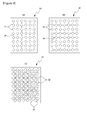
- Fig. 1 is a plane view illustrating an ITO thin film for a capacitive touch screen
- Fig. 2 is a plane view illustrating an operating mechanism of conventional capacitive touch screen.
- a conventional touch screen electrically senses a contact position of a finger.
- the finger which is a kind of conductive material, locates on an electrode, electric charges can gather between the electrode and the finger. If the electric charges gather, it is possible to measure capacitance between the finger and the electrode, so as to note the finger's touch indirectly.
- the electrodes of the touch screen may be formed of transparent conductive material, such as ITO (Indium Tin Oxide).
- transparent electrode patterns vertically aligned are provided.
- the vertically aligned transparent electrode patterns are provided on a transparent film 11 made of plastic sheet or glass, and they consist of first nod patterns 12 and first connecting patterns 13 which connect the first nod patterns 12 vertically.
- FIG. 1 In (b) of Fig. 1 , other transparent electrode patterns horizontally aligned (along x-axis) are provided.
- the conventional touch screen may be provided by overlaying the ITO transparent sheets of (a) and (b).
- ITO transparent sheets of (a) and (b) One example of the overlaid structure of the two transparent sheets mutually bonded is illustrated in (c) of Fig. 1 .
- the second nod patterns 15 and the first nod patterns 12 are positioned alternately, such that the connecting patterns connecting the first or second nod patterns intersect up and down. These connecting patterns may be electrically separated by the transparent insulating sheet.
- a signal intense passing through the electrode patterns aligned vertically and horizontally may be changed in accordance with the finger's contact position, such that the coordinates can be calculated by using the changes of the signal intense.
- the coordinates of the intersecting position 25 may be the position of the finger's contact.
- electric signal may be generated by the change of the capacitance of the transparent electrode pattern at the finger's contact position 22, to be transmitted to a controller for deciding the coordinates of the contact point.
- the transparent electrode patterns made of ITO are conductive, but of having high resistance in comparison with general metal.
- the present invention provides a touch panel sensor which can easily sense a weak signal so as to have an outstanding sensitivity even though using an electrode made of a relatively high resistance coefficient.
- the present invention provides a touch panel sensor which can be applied to a large size of touch screen, even though using an electrode made of a relatively high resistance coefficient.
- the present invention provides a touch panel sensor which has a high signal sensitivity, less limitation to enlargement of screen, less effect on transparency and clearance of a touch screen, even though using an transparent electrode made of high resistance.
- a touch panel sensor for sensing a contact position of part of body, comprises a substrate, a resist electrode part and a signal electrode part.
- the resist electrode part includes resist electrodes formed on the substrate to have a capacitance changeable according to approaching of the part of body, and the signal electrode part includes signal electrodes formed above the resist electrode having resistance coefficient less than the resist electrode.
- the electric signal generated from the resist electrode part is transferred to the signal electrode part. Since the signal electrode part has a relatively low resistance, the touch panel sensor of this invention can transfer weak signals easily, and may have a large touch screen area.
- the touch panel sensor may be used as a touch screen or a general touch pad.
- the substrate may be formed using transparent synthetic material, such as polyethylene, polypropylene, acryloyl, PET and the like, and glass.
- the substrate may not be transparent material, in case of being used, for example, to a touch pad for notebook computer or pointing device with stylus pen.
- the resist electrode part may be selected considering its optical character, similar to the substrate. Particularly, if optical character is not necessary, the resist electrode may be formed with gold, silver, aluminum and other metal or alloy, otherwise, if transparency is necessary, it may by formed with ITO or IZO (Indium Zinc Oxide).
- the resist electrode may be made of transparent conductive material, such as ITO, IZO, carbon nano tube (CNT), ultra thin metal pattern ( ⁇ 100 ⁇ ).
- transparent conductive material such as ITO, IZO, carbon nano tube (CNT), ultra thin metal pattern ( ⁇ 100 ⁇ ).
- the resist electrode made of the above materials may have an extremely high resistance, in case that the electrode is too long and narrow or the touch screen is too broad and large.
- metallic signal electrode part may overcome these problems.
- the resist electrode part may comprise first electrode patterns provided parallel on one surface of the substrate, and the signal electrode part may comprise second electrode patterns provided perpendicular to the first electrode patterns on the same surface of the substrate, to be electrically separated from the first electrode patterns, transparent connections formed over the first electrode patterns, and a low-resist line formed on the transparent connections arranged in series, such that the low-resist line can decrease the resistance of the second electrode patterns.
- a low-resist line may be formed on transparent connections to electrically connect them.
- the low-resist line may be a continuous conductive line, otherwise may be discontinuously interrupted electrode lines to be arranged or scattered to electrically connect electrodes or connections.
- the first electrode patterns and the second electrode patterns may be formed on the same surface of a transparent substrate, or may be formed on facing surfaces or opposite surfaces of the substrate.
- the electrode patterns may be formed on a bottom surface of the substrate, or in case that another substrate is provided under a glass plate additionally, the electrode patterns may be formed on a top surface of the substrate.
- the first electrode patterns may be arranged horizontally or vertically.
- the first electrode patterns may include enlarged portions and bridge portions. Otherwise, the first electrode patterns may be formed in a shape of a lane having a uniform width.
- the enlarged portion may be formed in a shape of rectangular, cube, diamond, circle or the like, which has a width relatively wider than the bridge portion.
- the normal capacitance may be decided by the intersection area of the bridge portion and the low-resist line.
- the bridge portion may be formed with a width of about 100 ⁇ 300 ⁇ m.
- the second electrode patterns are formed in a direction, preferably perpendicular to the first electrode patterns. Otherwise the second electrode patterns may be formed in a direction declined to the first electrode patterns, not parallel. Transparent connections may be formed in area electrically and physically separated from the first electrode patterns, and may be connected by the low-resist line.
- the second electrode patterns may be formed over or under the first electrode patterns. Also, since insulating layer or insulating patterns of 0.1 ⁇ 1.0 ⁇ m are interposed between the bridge portion and the low-resist line, the bridge portion intersecting to the low-resist line may be formed with a considerably narrow width.
- the low-resist line may be formed with a width less than about 30 ⁇ m, preferably less than about 10 ⁇ m, not to be seen by unaided eye and to have a considerably low resistance in comparison to conventional transparent electrodes. Moreover, the resistance of the low-resist line may be lowed by increasing its thickness.
- the low-resist line may be formed using gold, silver, aluminum, nickel, titanium and the other metal or its alloy.
- the touch panel sensor of this invention uses the signal electrode part having a resistance coefficient less than the resist electrode part, such that the touch panel sensor transfers touch signal easily and is suitable for a large scale touch screen.
- the touch panel sensor of this invention has a good signal sensitivity, transparency and clearance.
- Fig. 3 is a plane view illustrating a touch panel sensor according to the first embodiment of this invention.
- a touch panel sensor comprises a transparent sheet 101, which is provided with a substrate 110, a resist electrode part 120 and a signal electrode part 130.
- the substrate 110 is provided in a shape of a thin film, using insulating material such as transparent plastic sheet or glass.
- the resist electrode part 120 includes resist electrodes 121 aligned vertically (along y-axis) on the substrate to have a capacitance changeable according to approaching of part of body.
- the resist electrode part 120 may be formed using transparent conductive material like ITO or IZO.
- the resist electrodes 121 of the resist electrode part 120 are connected vertically by connecting patterns 122.
- the resist electrodes 121 and the connecting patterns 122 in one row may be formed integrated as one body.
- the signal electrode part 130 comprises signal electrodes 131, which is provided in a shape of line to electrically connect the resist electrodes 121 and the connecting patterns 122 in a vertical row, formed thereon.
- the signal electrodes 131 may be narrower than the resist electrodes 121 and the connecting patterns 122.
- the signal electrode part 130 may have a resistance coefficient less than that of the resist electrode part 120, such as gold, silver, aluminum and other metal.
- the metallic signal electrode part 130 may have a high conductivity, but may hide light from LCD monitor or other display device because metal usually blocks out light. However, if the signal electrodes are too fine, user can not recognize the signal electrodes and feel unchanged brightness due to light's scattering and diffraction.
- the signal electrode part 130 is provided on the resist electrodes 121 and the connecting patterns 122 vertically aligned, in a shape of a straight line. Otherwise, the signal electrode part may be formed in a shape of a not-straight line, along a contour of the resist electrodes and in various shapes.
- One or more signal electrodes 131 may be provided on a set of the resist electrodes 121 and the connecting patterns 122.
- the touch panel sensor of this embodiment may produced by overlaying and adhering two of the above mentioned transparent sheets 101.
- the touch panel sensor may be provided by overlaying two sheet, one sheet where the electrode parts are aligned vertically and the other sheet where the electrode parts are aligned horizontally.
- horizontally aligned resist electrodes and vertically aligned resist electrodes are arranged alternately and the connecting patterns of two sheets cross to be electrically separated.
- the signal electrode part may be provided on the resist electrodes of one sheet. In case of forming the resist electrodes on both sides of one sheet, the signal electrode part may be provided just on one side of the sheet.
- the resist electrode parts 120 located at touched position may have different signal reactions to recognize the coordinates (x, y) of the touched position.
- horizontally and vertically aligned resist electrode parts 120 can have changed signals, the touch panel sensor or the device can calculate x- and y- average amounts to decide the coordinates of the contact position.
- Figs. 4 to 8 are drawings illustrating a manufacturing method according to the first embodiment of the invention.
- the resist electrode part 120 including the resist electrodes 121 is formed on the substrate 110.
- the resist electrode part 120 can be treated by photoresist and etching processes to form the patterns shown in Fig. 4 .
- a thin metal layer 140 is formed on the substrate 110 where the resist electrode part 120 is formed.
- a photoresist layer 150 is formed on the thin metal layer 140.
- the photoresist layer 150 may be treated by patterning process.
- the photoresist layer 150 may be a positive type and be exposed to light, such as laser, passing through a mask 160. Part of the photoresist layer 150 not exposed to light may be removed to form a photoresist pattern 155 as shown in Fig. 8 .
- part of the metal layer 140 exposed through the photoresist pattern 155 may be removed.
- the signal electrode part 130 may be formed as shown in Fig. 9 .
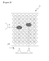
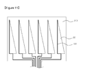
- Fig. 10 is a plane view illustrating a touch panel sensor according to second embodiment of this invention.
- a touch panel sensor comprises a sheet 210, a resist electrode part 220 including vertical nod patterns 221 ⁇ 228 formed on the sheet 210, and a signal electrode part 230 including signal electrodes 231 and 232 formed on the vertical nod patterns 221 ⁇ 228.
- the vertical nod patterns 221 ⁇ 228 are aligned vertically, about 6 lines of the vertical nod patterns are provided on the sheet.
- the vertical nod patterns 221 ⁇ 228 have a first nod pattern 221a (or 222a) and a second nod pattern 221b (or 222b).
- the vertical nod patterns 221 ⁇ 228 may be provided in a shape of diamond or cube, and each of the vertical nod patterns 221 ⁇ 228 may be divided into the first nod pattern and the second nod pattern.
- the area ratios of the first nod patterns and the second nod patterns may be varied, such as (1:8), (2:7), (3:6), (4:4), (5:4), (6:3), (7:2), (8:1).
- the first nod patterns 221a and 222a are connected by a first connecting pattern 229a, and area of the first nod patterns, from up to down, increase by steps.
- the second nod patterns 221b and 222b are connected by a second connecting pattern 229b, and area of the second nod patterns, from up to down, decrease by steps.
- the sheet 210 of this embodiment may be formed using transparent synthetic material, such as polyethylene, polypropylene, acryloyl, PET and the like, and glass. Otherwise, the sheet may not be transparent material, in case of being used, for example, to a touch pad for notebook computer or pointing device with stylus pen.
- the material for the vertical nod patterns 221 ⁇ 228 may be selected variously.
- the vertical nod patterns are made of ITO or IZO.
- the resist electrode part may be formed using other conductive material, such as gold, silver, aluminum and the like.
- the first nod patterns 221a and 222a are mutually connected, and the second nod patterns 221b and 222b are mutually connected.
- the signal electrodes 231 and 232 of the signal electrode part 230 are formed on the vertical nod patterns 221 to 228 vertically arranged to connect the vertical nod patterns 221 to 228. Particularly, one of the signal electrode 231 is formed on the first nod patterns 221a and 222a and the first connecting pattern 229a, and the other of the signal electrode 232 is formed on the second nod patterns 221b and 222b and the second connecting pattern 229b.
- the signal electrodes 231 and 232 is narrower than the fist and the second nod patterns, and also narrower than the first and second connecting partterns 229a and 229b.
- the signal electrodes 231 and 232 are formed using conductive material having a resistance coefficient less than the resist electrode part 220, made of ITO or IZO.
- the signal electrodes 231 and 232 may be formed using gold, silver, aluminum and the like.
- the signal electrodes 231 and 232 are not transparent, they are extremely fine rather than the nod patterns and the connecting patterns, so as to be applied to a transparent touch screen and take no effect to transparency and clearance.
- the signal sensitivity of the touch panel sensor of this embodiment is very excellent.
- the touch screen according to the present invention can be freely enlarged.
- a final x-coordinate can be calculated on an average of the pre-calculated x-coordinates.
- one exemplary equation may be 1/2 ⁇ ( ⁇ nlk*k)/( ⁇ n1k) + ( ⁇ n2k*k)/( ⁇ n2k) ⁇ , wherein k is a line number of the nod patterns, and n1k and n2k are signal intense at the first and second nod patterns according to k line.
- the y-coordinate of the finger contact position can be decided by comparing the signal result measured via the first nod pattern and the second nod pattern, which form a pair. For reference, when the finger contacts with the first and the second nod patterns simultaneously, the signal intense transferred to a controller is proportional to the size of the contact area.
- finger contact area and signal intense at the first nod pattern is A(y) and C(y) respectively and finger contact area and signal intense at the second nod pattern is B(y) and D(y) respectively.
- the controller or the device calculates C(y)/D(y), compares it with A(y)/B(y), and reverse the amount of y referring a table.
- the table can be defined that if y (O ⁇ y ⁇ 1) is 0.5, A(0.5)/B(0.5) can be 1, if y is 1.0 (at top point), A(1)/B(1) can be 1/8, and if y is zero (at bottom point), A(0)/B(0) can be 8.
- y-coordinate can be calculated from A(y)/B(y).
- a signal intense of the first nod pattern of 4th line is 60
- a signal intense of the first nod pattern of 5th line is 70
- a signal intense of the first nod pattern of the other lines is 0
- a signal intense of the second nod pattern of 3rd line is 80
- a signal intense of the second nod pattern of 4th line is 100
- a signal intense of the second nod pattern of 5th line is 90
- a signal intense (C(y)) of the first nod patterns is 130
- a signal intense (D(y)) of the second nod patterns is 190
- C(y)/(D(y) is approximately 0.68.
- y when A(y)/B(y) is 0.68, y can be 0.65. In case that the vertical length of a touch panel sensor is 100mm, y-coordinate can be calculated as about 65mm.
- Fig. 11 is a drawing illustrating a touch panel sensor according to the third embodiment of this invention.
- the touch panel sensor according to the third embodiment may be similar to the touch panel sensor according to the second embodiment.
- the description for the touch panel sensor of the third embodiment can refer the description and drawings for the touch panel sensor of the second embodiment, and repeated matters can be skipped.
- a resist electrode part 320 of the third embodiment is different from the resist electrode part 220 of the second embodiment.
- resist electrode 321 included in the resist electrode part 320 are arranged on a substrate 310 parallel in one direction, and each of the resist electrodes 321 has a tapering shape.
- each of the resist electrodes 321 is formed in a right-triangle shape, and the resist electrodes 321 are arranged along horizontally and uniformly.
- a signal electrode part includes signal electrodes 331 formed on the resist electrodes 321.
- the substrate 310 is formed using transparent material, and the resist electrodes 321 are formed using ITO, IZO and the like for a touch screen.
- the signal electrodes 331 is formed along an edge of the resist electrode and in a shape of a fine and uniform line.
- the signal electrodes 331 may be formed using a low resistance material less than the resist electrode part 320, such as gold, silver, aluminum and the like.
- the signal electrodes 331 are not transparent, they are provided in a fine line shape, so as to be applied to a transparent touch screen and take no effect to transparency and clearance.
- the signal sensitivity of the touch panel sensor of this embodiment is very excellent.
- the touch screen according to this embodiment can be freely enlarged.
- the change of the capacitance is different in accordance with the finger's contact point to be used to calculate y-coordinate.
- the resist electrode 321 having a changed capacitance can be used to calculate x-coordinate.
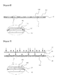
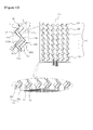
- Fig. 12 is a plane view illustrating a touch panel sensor according to the fourth embodiment of this invention
- Figs. 13 to 15 are partially enlarged perspective view illustrating a manufacturing method of the touch panel sensor of Fig. 12 .
- a touch panel sensor 400 comprises a transparent substrate 410, first electrode patterns 420 and second electrode patterns 430 formed on the substrate 410, and insulating patterns 440 interposed between the first electrode patterns 420 and the second electrode patterns 430.
- the substrate 410 may be formed using synthetic film, such as PET, PC, PE and the like, and glass substrate.
- the substrate 410 may be installed on the display like LCD or LED display module, otherwise may be applied directly to a transparent sheet or film composing the LCD or LED display module.
- the transparency of the transparent substrate 410 can mean little opaque state only not to prevent display function, besides perfectly clear state.
- the first electrode patterns 420 and the second electrode patterns 430 may be formed one or both of the top side and bottom side of the substate 410.
- the both electrode patterns may be formed on a top side of the film, however, in case of glass substrate they may be formed on a bottom side of the glass substrate.
- the first electrode patterns 420 may be formed using transparent conductive material, such as ITO, IZO or carbon nano tube (CNT), and may be provided in a shape of line patterns arranged parallel on the substrate 410, horizontally or vertically.
- the first electrode patterns 420 may include enlarged portions 422 and bridge portions 424 provided alternately in series. The enlarged portions 422 and the bridge portions 424 aligned alternately in one row, may be formed using the same or different material.
- the enlarged portions 422 have a width relatively or considerably wider than the bridge portions 424, and the bridge portions 424 is located between every enlarged portions 422 to electrically connect the enlarged portions 422.
- the bridge portions 424 may be formed with a width of about 0.1 ⁇ 0.2mm and the enlarged portions 422 may be formed with a width of about 4 ⁇ 6mm. In this instance, the enlarged portions 422 have a width of about 20 ⁇ 60 times wider than the bridge portions 424.
- the enlarged portions 422 and the bridge portions 424 may be formed in rectangular shape, otherwise may be formed in diamond, circle or oval.
- the enlarged portions 422 and the bridge portions 424 may be formed with the same material or on the same surface together with transparent connections 436, and may be formed in a various shape only to be electrically separated from each other.
- the display under the touch panel sensor 400 can generate electromagnetic interference (EMI), but if the electrode patterns 420 and 430 and the transparent connections 436 are separated by minimum distance, they can reduce the EMI.
- EMI electromagnetic interference
- the second electrode patterns 430 may partially overlay the first electrode patterns 420.
- the second electrode patterns 430 may be formed over or under the first electrode patterns 420 to be electrically separated from the first electrode patterns 420.
- an insulating layer or insulating patterns 440 may be formed between the first and the second electrode patterns 420 and 430.
- the insulating patterns 440 may be formed using insulating material, such as SiO 2 , Si 3 N 4 or TiO 2 , and may be formed by vaporization, sputtering, applying, spraying, laminating, adhesion, printing and the like. As shown in drawings, the insulating patterns 440 may be provided indirectly by patterning process after vaporization or sputtering, otherwise, may be provided directly by printing without patterning. The insulating patterns 440 may be provided as one insulating layer. As shown in Fig. 14 , after the enlarged portions 422, the bridge portions 424 and the transparent connections 436 are patterned, the insulating patterns 440 may be formed by another patterning process.
- insulating material such as SiO 2 , Si 3 N 4 or TiO 2
- the second electrode patterns 430 include the transparent connections 436 and a low-resist line 434.
- the transparent connections 436 may be formed with the first electrode patterns 420 simultaneously.
- the transparent connections 436 may be formed with transparent conductive material to have a width of about 0.1 ⁇ 0.2mm, which can be formed by photoresist process etching ITO layer, together with the enlarged portions 422 and the bridge portions 424.
- the low-resist line 434 is formed on the insulating patterns 440, and passes top surfaces of the transparent connections 436 to electrically connect the transparent connections 436.
- the low-resist line 434 may be formed using metal like gold, silver, aluminum or chrome, or may be formed by patterning process after vaporization or sputtering, or may be formed by printing process like silkscreen or inkjet.
- the low-resist line 434 may be formed with a width less than about 30 ⁇ m, preferably less than about 10 ⁇ m, not to be seen by unaided eye.
- the low-resist line 434 may be formed in a shape of a straight line, otherwise may be formed in a shape of a curved line or a folded line, may be changed regularly or irregularly. In case that the low-resist line 434 is formed in a shape of a irregularly curved or folded line, it cannot be seen from outside.
- the low-resist line 434 may be formed together with wire patterns 450 located at bezel area.
- the wire patterns 450 of the bezel area are focused on one side of the transparent substrate 410 to be connected to FPCB. Since the wire patterns 450 are formed with metal, it can be formed simultaneously with the low-resist line 434.
- Fig. 16 is a sectional view illustrating an overlaid structure of the touch panel sensor of Fig. 12 .
- the low-resist line 434 formed with metal is provided on the transparent substrate 410, the bridge portions 424 and the insulating patterns 440.
- the transparent conductive material like ITO has an area resistance of about 250 ⁇ /square
- the transparent material of a width of about 100 ⁇ 300 ⁇ m and a length of about 6 ⁇ 8cm may have a resistance of several hundred ohm.
- conventional ITO electrodes are not proper to a large scale display because of extremely high resistance.
- the metallic low-resist line 434 is formed with metal, it can reduce the total resistance of the second electrode patterns 430, to improve the sensor's sensitivity.
- the normal capacitance may be decided by the intersection area of the bridge portion 424 and the low-resist line 434.
- OCA optical clearance adhesive
- the bridge portions 424 and the low-resist line 434 are separated by a gap of about 0.1 ⁇ 1.0 ⁇ m through the insulating patterns 440, so as to form a capacitance of about 200 ⁇ 1000 times larger than the conventional touch panel sensor.
- the second electrode patterns 430 may be located below the first electrode patterns 420.
- the low-resist line 434 may have less resistance by increasing its thickness, with taking no effect to transparency of the touch screen. Namely, the low-resist line of this embodiment can control the resistance freely without damaging transparency and clearance.
- the low-resist line 434 of this embodiment is shaped of a straight line, however, it can be shaped of regularly or irregularly curved line or folded line not to be seen by unaided eye.
- the low-resist line 434 may further have optical absorption.
- optical absorption In case of forming a minute dark or anti-reflection pattern on the low-resist line 434, for example with carbon/titanium (Cu/Ti), molybdenum (Mo), chrome (Cr), black chrome and the like.
- the low-resist line itself may be made of dark metal, such as Cu/Ti, Mo, Cr and the like.
- the low-resist line 434 is formed on a top side of the first electrode patterns 420 and the transparent connections 436, alternatively the low-resist line may be formed on a bottom side of them.
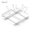
- Fig. 17 is a plane view illustrating a touch panel sensor according to the fifth embodiment of this invention.
- a touch panel sensor 500 comprises a transparent substrate 510, first electrode patterns 520 and second electrode patterns 530 formed on the substrate 510, and insulating patterns 540 interposed between the first electrode patterns 520 and the second electrode patterns 530.
- the transparent substrate 510 may be formed using synthetic film or glass substrate, the first electrode patterns 520 include enlarged portion 522 and bridge portions 524, and the second electrode patterns 530 include a low-resist line 534 and transparent connections 536.
- the first electrode patterns 520 include enlarged portion 522 and bridge portions 524
- the second electrode patterns 530 include a low-resist line 534 and transparent connections 536.
- the second electrode patterns 530 include the low-resist line 534 and the transparent connections 536, which are aligned in one row.
- two or more low-resist lines 534 are grouped to form an electrode, in which top or bottom ends of the low-resist lines are electrically connected.
- 3 low-resist lines form a group to serve as an independent low-resist line.
- the low-resist lines 434 of Fig. 12 are arranged by a distance of about 5mm, however, the low-resist lines 534 of this embodiment are arranged by a distance of about 1.7 ⁇ 1.0mm, such that three of the lines 534 are electrically connected at top and bottom ends.
- Two or more of the low-resist lines 534 are grouped to help a instant calculation of the finger's precise position.
- the pattern lines are parallel connected, and each of the low-resist lines 534 in the same group is separated enough, so at to improve the sensitivity according to the changing of the capacitance.
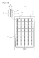
- Fig. 18 is a plane view illustrating a touch panel sensor according to the sixth embodiment of this invention.
- a touch panel sensor 600 comprises a transparent substrate 610, first electrode patterns 620 and second electrode patterns 630 formed on the substrate 610, and insulating patterns 640 interposed between the first electrode patterns 620 and the second electrode patterns 630.
- the transparent substrate 610 may be formed using synthetic film or glass substrate, the first electrode patterns 620 include enlarged portion 622 and bridge portions 624, and the second electrode patterns 630 include a low-resist line 634 and transparent connections 636.
- the first electrode patterns 620 include enlarged portion 622 and bridge portions 624
- the second electrode patterns 630 include a low-resist line 634 and transparent connections 636.
- the enlarged portions 622 are formed in a shape of circle or oval, and the transparent connections 636 are formed in a shape having concave sides corresponding to the enlarged portions 622.
- the low-resist line 634 may be formed is a shape of irregularly folded line on the transparent connections 636.
- the first electrode patterns 620 and the transparent connections 636 are shaped for mutual harmony to be separated by minimum distance, such that they can reduce electromagnetic interference (EMI) and improve the sensitivity of the sensor.
- EMI electromagnetic interference
- Fig. 19 is a partially enlarged perspective view illustrating a touch panel sensor according to the seventh embodiment of this invention.
- the touch panel sensor of this embodiment further comprises low-resist patterns 460 formed on or in the first electrode patterns 420.
- the low-resist patterns 460 may be formed enlarged portions 422 or bridge portions 424, and may be formed using conductive material having a low resistance less than transparent conductive material like ITO.
- the low-resist lines 434 and the low-resist patterns 460 may be formed using the same metal.
- the low-resist patterns 460 may be formed horizontally along the first electrode patterns 420, so at to reduce total resistance of the first electrode patterns 420.
- the low-resist patterns 460 may be formed to have a thickness of less than 100 ⁇ to permit light to pass through itself.
- the low-resist patterns 460 may be formed in a shape of a straight line, otherwise, may be formed in a shape of repeatedly curved or folded line, regularly or irregularly.
- Fig. 20 is a partially enlarged perspective view illustrating a touch panel sensor according to the eighth embodiment of this invention.
- the touch panel sensor of this embodiment further comprises low-resist patterns 465 arranged discontinuously on the first electrode patterns 420.
- the discontinuous low-resist patterns 465 may be formed on the enlarged portions 422 or the bridge portions 424, using conductive material having a low resistance less than transparent conductive material like ITO.
- the low-resist patterns 465 of this embodiment may be formed wholly or partially on a top or bottom side of the first electrode patterns 420.
- the low-resist patterns 465 may be formed parallel to the first electrode patterns 420, otherwise may be formed irregularly.
- the low-resist line 434-1 may be formed on the transparent connections discontinuously.
- the low-resist patterns 465 and the low-resist lines 434-1 may work to reduce total resistance of the first electrode patterns 420 and the transparent connections 436, to be arranged or scattered on the low-resist members 465 and 434-1.
- ends of each of the low-resist patterns 465 may be partially overlapped.
- the discontinuously provided low-resist patterns 465 and low-resist lines 434-1 may be arranged regularly, however, according to the present embodiment, they may be provided irregularly for invisibility.
- the touch panel sensor of this invention can be used to a display module to sense a contact position of part of body.
Landscapes
- Engineering & Computer Science (AREA)
- General Engineering & Computer Science (AREA)
- Theoretical Computer Science (AREA)
- Human Computer Interaction (AREA)
- Physics & Mathematics (AREA)
- General Physics & Mathematics (AREA)
- Position Input By Displaying (AREA)
Abstract
Description
- This invention relates to a touch panel sensor, more particularly, relates to a touch panel sensor which can sense a precise touch position of a finger on a flat plate.
-
Fig. 1 is a plane view illustrating an ITO thin film for a capacitive touch screen, andFig. 2 is a plane view illustrating an operating mechanism of conventional capacitive touch screen. - Referring to
Fig. 1 , a conventional touch screen electrically senses a contact position of a finger. When the finger which is a kind of conductive material, locates on an electrode, electric charges can gather between the electrode and the finger. If the electric charges gather, it is possible to measure capacitance between the finger and the electrode, so as to note the finger's touch indirectly. - Not to hide a liquid crystal display or another display, the electrodes of the touch screen may be formed of transparent conductive material, such as ITO (Indium Tin Oxide).
- In (a) of
Fig. 1 , transparent electrode patterns vertically aligned (along y-axis) are provided. The vertically aligned transparent electrode patterns are provided on a transparent film 11 made of plastic sheet or glass, and they consist of first nod patterns 12 and first connecting patterns 13 which connect the first nod patterns 12 vertically. - In (b) of
Fig. 1 , other transparent electrode patterns horizontally aligned (along x-axis) are provided. The horizontally aligned transparent electrode patterns provided on another transparent film 14, consist of second nod patterns 15 and second connecting patterns 16 which connect the second nod patterns 15 horizontally. - Generally the conventional touch screen may be provided by overlaying the ITO transparent sheets of (a) and (b). One example of the overlaid structure of the two transparent sheets mutually bonded is illustrated in (c) of
Fig. 1 . - As shown, the second nod patterns 15 and the first nod patterns 12 are positioned alternately, such that the connecting patterns connecting the first or second nod patterns intersect up and down. These connecting patterns may be electrically separated by the transparent insulating sheet.
- According to the touch screen structure of (c) of
Fig. 1 , a signal intense passing through the electrode patterns aligned vertically and horizontally may be changed in accordance with the finger's contact position, such that the coordinates can be calculated by using the changes of the signal intense. - In detail, after deciding the x- and y- coordinates using the signal intenses 23 and 24 of the electrode patterns, the coordinates of the intersecting position 25 may be the position of the finger's contact.
- In this instance, electric signal may be generated by the change of the capacitance of the transparent electrode pattern at the finger's
contact position 22, to be transmitted to a controller for deciding the coordinates of the contact point. The transparent electrode patterns made of ITO (Indium Tin Oxide) are conductive, but of having high resistance in comparison with general metal. - Since the signal loss by the resistance of the electrode pattern is proportional to area and length of the electrode pattern, manufacturers have a limit to enlarge the size of the touch screens.
- The present invention provides a touch panel sensor which can easily sense a weak signal so as to have an outstanding sensitivity even though using an electrode made of a relatively high resistance coefficient.
- The present invention provides a touch panel sensor which can be applied to a large size of touch screen, even though using an electrode made of a relatively high resistance coefficient.
- The present invention provides a touch panel sensor which has a high signal sensitivity, less limitation to enlargement of screen, less effect on transparency and clearance of a touch screen, even though using an transparent electrode made of high resistance.
- According to one exemplary embodiment of this invention, a touch panel sensor for sensing a contact position of part of body, comprises a substrate, a resist electrode part and a signal electrode part.
- The resist electrode part includes resist electrodes formed on the substrate to have a capacitance changeable according to approaching of the part of body, and the signal electrode part includes signal electrodes formed above the resist electrode having resistance coefficient less than the resist electrode. The electric signal generated from the resist electrode part is transferred to the signal electrode part. Since the signal electrode part has a relatively low resistance, the touch panel sensor of this invention can transfer weak signals easily, and may have a large touch screen area.
- The touch panel sensor may be used as a touch screen or a general touch pad. In case of being used as touch screens, the substrate may be formed using transparent synthetic material, such as polyethylene, polypropylene, acryloyl, PET and the like, and glass. The substrate may not be transparent material, in case of being used, for example, to a touch pad for notebook computer or pointing device with stylus pen.
- The resist electrode part may be selected considering its optical character, similar to the substrate. Particularly, if optical character is not necessary, the resist electrode may be formed with gold, silver, aluminum and other metal or alloy, otherwise, if transparency is necessary, it may by formed with ITO or IZO (Indium Zinc Oxide).
- The resist electrode may be made of transparent conductive material, such as ITO, IZO, carbon nano tube (CNT), ultra thin metal pattern (<100Å). However, since the above materials have a high resistance coefficient rather than metal, the resist electrode made of the above materials may have an extremely high resistance, in case that the electrode is too long and narrow or the touch screen is too broad and large. But, according to this invention, metallic signal electrode part may overcome these problems.
- The resist electrode part may comprise first electrode patterns provided parallel on one surface of the substrate, and the signal electrode part may comprise second electrode patterns provided perpendicular to the first electrode patterns on the same surface of the substrate, to be electrically separated from the first electrode patterns, transparent connections formed over the first electrode patterns, and a low-resist line formed on the transparent connections arranged in series, such that the low-resist line can decrease the resistance of the second electrode patterns.
- In this specification, a low-resist line may be formed on transparent connections to electrically connect them. The low-resist line may be a continuous conductive line, otherwise may be discontinuously interrupted electrode lines to be arranged or scattered to electrically connect electrodes or connections.
- The first electrode patterns and the second electrode patterns may be formed on the same surface of a transparent substrate, or may be formed on facing surfaces or opposite surfaces of the substrate. For example, in case that the substrate is made of enforced glass, the electrode patterns may be formed on a bottom surface of the substrate, or in case that another substrate is provided under a glass plate additionally, the electrode patterns may be formed on a top surface of the substrate.
- The first electrode patterns may be arranged horizontally or vertically. Preferably, the first electrode patterns may include enlarged portions and bridge portions. Otherwise, the first electrode patterns may be formed in a shape of a lane having a uniform width.
- Using the first electrode pattern having the enlarged portion and the bridge portion, the enlarged portion may be formed in a shape of rectangular, cube, diamond, circle or the like, which has a width relatively wider than the bridge portion. In normal state that the objective does not approach to the touch screen, the normal capacitance may be decided by the intersection area of the bridge portion and the low-resist line. However, in the event that the objective approach, the change of the capacitance may occur through the enlarged portions. The bridge portion may be formed with a width of about 100∼300µm.
- The second electrode patterns are formed in a direction, preferably perpendicular to the first electrode patterns. Otherwise the second electrode patterns may be formed in a direction declined to the first electrode patterns, not parallel. Transparent connections may be formed in area electrically and physically separated from the first electrode patterns, and may be connected by the low-resist line.
- Since the capacitance at the cross section between the first and second electrode patterns can be effected by the enlarged portion, the second electrode patterns may be formed over or under the first electrode patterns. Also, since insulating layer or insulating patterns of 0.1∼1.0µm are interposed between the bridge portion and the low-resist line, the bridge portion intersecting to the low-resist line may be formed with a considerably narrow width.
- The low-resist line may be formed with a width less than about 30µm, preferably less than about 10µm, not to be seen by unaided eye and to have a considerably low resistance in comparison to conventional transparent electrodes. Moreover, the resistance of the low-resist line may be lowed by increasing its thickness. The low-resist line may be formed using gold, silver, aluminum, nickel, titanium and the other metal or its alloy.
- The touch panel sensor of this invention uses the signal electrode part having a resistance coefficient less than the resist electrode part, such that the touch panel sensor transfers touch signal easily and is suitable for a large scale touch screen.
- The touch panel sensor of this invention has a good signal sensitivity, transparency and clearance.
-
-
Fig. 1 is a plane view illustrating an ITO thin film for a capacitive touch screen, -
Fig. 2 is a plane view illustrating an operating mechanism of conventional capacitive touch screen, -
Fig. 3 is a plane view illustrating a touch panel sensor according to the first embodiment of this invention, -
Figs. 4 to 9 are drawings illustrating a manufacturing method according to the first embodiment of the invention, -
Fig. 10 is a plane view illustrating a touch panel sensor according to second embodiment of this invention, -
Fig. 11 is a drawing illustrating a touch panel sensor according to the third embodiment of this invention, -
Fig. 12 is a plane view illustrating a touch panel sensor according to the fourth embodiment of this invention, -
Figs. 13 to 15 are partially enlarged perspective view illustrating a manufacturing method of the touch panel sensor ofFig. 12 , -
Fig. 16 is a sectional view illustrating an overlaid structure of the touch panel sensor ofFig. 12 , -
Fig. 17 is a plane view illustrating a touch panel sensor according to the fifth embodiment of this invention, -
Fig. 18 is a plane view illustrating a touch panel sensor according to the sixth embodiment of this invention, -
Fig. 19 is a partially enlarged perspective view illustrating a touch panel sensor according to the seventh embodiment of this invention, and -
Fig. 20 is a partially enlarged perspective view illustrating a touch panel sensor according to the eighth embodiment of this invention. - Below with reference to the attached drawings, preferred one exemplary embodiment of present invention is described in detail, but present invention is not limited or restricted by one exemplary embodiment of present invention. For reference, same number means same element practically, wherein may explain quoting the content mentioned at another drawing according to this rule, and the obvious and repeated contents are skipped to dealer.
-
Fig. 3 is a plane view illustrating a touch panel sensor according to the first embodiment of this invention. - Referring to
Fig. 3 , a touch panel sensor comprises atransparent sheet 101, which is provided with asubstrate 110, a resistelectrode part 120 and asignal electrode part 130. - The
substrate 110 is provided in a shape of a thin film, using insulating material such as transparent plastic sheet or glass. - The resist
electrode part 120 includes resistelectrodes 121 aligned vertically (along y-axis) on the substrate to have a capacitance changeable according to approaching of part of body. The resistelectrode part 120 may be formed using transparent conductive material like ITO or IZO. - The resist
electrodes 121 of the resistelectrode part 120 are connected vertically by connectingpatterns 122. The resistelectrodes 121 and the connectingpatterns 122 in one row may be formed integrated as one body. - The
signal electrode part 130 comprisessignal electrodes 131, which is provided in a shape of line to electrically connect the resistelectrodes 121 and the connectingpatterns 122 in a vertical row, formed thereon. Thesignal electrodes 131 may be narrower than the resistelectrodes 121 and the connectingpatterns 122. - The
signal electrode part 130 may have a resistance coefficient less than that of the resistelectrode part 120, such as gold, silver, aluminum and other metal. - The metallic
signal electrode part 130 may have a high conductivity, but may hide light from LCD monitor or other display device because metal usually blocks out light. However, if the signal electrodes are too fine, user can not recognize the signal electrodes and feel unchanged brightness due to light's scattering and diffraction. - According to the present embodiment, the
signal electrode part 130 is provided on the resistelectrodes 121 and the connectingpatterns 122 vertically aligned, in a shape of a straight line. Otherwise, the signal electrode part may be formed in a shape of a not-straight line, along a contour of the resist electrodes and in various shapes. One ormore signal electrodes 131 may be provided on a set of the resistelectrodes 121 and the connectingpatterns 122. - The touch panel sensor of this embodiment may produced by overlaying and adhering two of the above mentioned
transparent sheets 101. For example, the touch panel sensor may be provided by overlaying two sheet, one sheet where the electrode parts are aligned vertically and the other sheet where the electrode parts are aligned horizontally. In case of overlaying twotransparent sheets 101, horizontally aligned resist electrodes and vertically aligned resist electrodes are arranged alternately and the connecting patterns of two sheets cross to be electrically separated. The signal electrode part may be provided on the resist electrodes of one sheet. In case of forming the resist electrodes on both sides of one sheet, the signal electrode part may be provided just on one side of the sheet. - In accordance with this touch panel sensor, the resist
electrode parts 120 located at touched position may have different signal reactions to recognize the coordinates (x, y) of the touched position. - According to a finger contact event, horizontally and vertically aligned resist
electrode parts 120 can have changed signals, the touch panel sensor or the device can calculate x- and y- average amounts to decide the coordinates of the contact position. - Hereinafter, a manufacturing method according to this embodiment is described.
-
Figs. 4 to 8 are drawings illustrating a manufacturing method according to the first embodiment of the invention. - At first, referring to
Fig. 4 , the resistelectrode part 120 including the resistelectrodes 121 is formed on thesubstrate 110. - After forming a transparent conductive layer, with ITO or IZO, on the
substrate 110, the resistelectrode part 120 can be treated by photoresist and etching processes to form the patterns shown inFig. 4 . - And then, as shown in
Fig. 5 , athin metal layer 140 is formed on thesubstrate 110 where the resistelectrode part 120 is formed. - And then, as shown in
Fig. 6 , aphotoresist layer 150 is formed on thethin metal layer 140. Thephotoresist layer 150 may be treated by patterning process. - Referring to
Fig. 7 , thephotoresist layer 150 may be a positive type and be exposed to light, such as laser, passing through amask 160. Part of thephotoresist layer 150 not exposed to light may be removed to form aphotoresist pattern 155 as shown inFig. 8 . - By etching, part of the
metal layer 140 exposed through thephotoresist pattern 155 may be removed. After removing thephotoresist pattern 155, thesignal electrode part 130 may be formed as shown inFig. 9 . -
Fig. 10 is a plane view illustrating a touch panel sensor according to second embodiment of this invention. - Referring to
Fig. 10 , a touch panel sensor comprises asheet 210, a resistelectrode part 220 includingvertical nod patterns 221∼228 formed on thesheet 210, and asignal electrode part 230 includingsignal electrodes vertical nod patterns 221∼228. Thevertical nod patterns 221∼228 are aligned vertically, about 6 lines of the vertical nod patterns are provided on the sheet. - The
vertical nod patterns 221∼228 have afirst nod pattern 221a (or 222a) and asecond nod pattern 221b (or 222b). Along a vertical line, thevertical nod patterns 221∼228 may be provided in a shape of diamond or cube, and each of thevertical nod patterns 221∼228 may be divided into the first nod pattern and the second nod pattern. For example, from up to down, the area ratios of the first nod patterns and the second nod patterns may be varied, such as (1:8), (2:7), (3:6), (4:4), (5:4), (6:3), (7:2), (8:1). - The
first nod patterns pattern 229a, and area of the first nod patterns, from up to down, increase by steps. Oppositely, Thesecond nod patterns pattern 229b, and area of the second nod patterns, from up to down, decrease by steps. - The
sheet 210 of this embodiment may be formed using transparent synthetic material, such as polyethylene, polypropylene, acryloyl, PET and the like, and glass. Otherwise, the sheet may not be transparent material, in case of being used, for example, to a touch pad for notebook computer or pointing device with stylus pen. - The material for the
vertical nod patterns 221∼228 may be selected variously. For example, according to this embodiment, the vertical nod patterns are made of ITO or IZO. But, the resist electrode part may be formed using other conductive material, such as gold, silver, aluminum and the like. - In the vertical nod patterns, the
first nod patterns second nod patterns - The
signal electrodes signal electrode part 230 are formed on thevertical nod patterns 221 to 228 vertically arranged to connect thevertical nod patterns 221 to 228. Particularly, one of thesignal electrode 231 is formed on thefirst nod patterns pattern 229a, and the other of thesignal electrode 232 is formed on thesecond nod patterns pattern 229b. - The
signal electrodes - The
signal electrodes electrode part 220, made of ITO or IZO. Thesignal electrodes - Although the
signal electrodes - Since the electric signal is transmitted via the
signal electrodes electrode part 220, the signal sensitivity of the touch panel sensor of this embodiment is very excellent. - Since the
signal electrode - Hereinafter, described are processes to calculate x-coordinate using the
vertical nod patterns 221 to 228. - Referring to
Fig. 10 , provided are 6 lines of thevertical nod patterns 221 to 228 vertically connected. The x-coordinate can be calculated by a math equation ((n1*1)+ (n2*2)+ ∼ (nk*k)}/(n1+ n2+∼ nk), wherein k is a number of the nod patterns and nk is a sum of signal intense at the first and second nod patterns according to k line. - In case that a signal intense of the first nod pattern of 4th line is 60, a signal intense of the first nod pattern of 5th line is 70, a signal intense of the first nod pattern of the other lines is 0, a signal intense of the second nod pattern of 3rd line is 80, a signal intense of the second nod pattern of 4th line is 100, and a signal intense of the second nod pattern of 5th line is 90, x-coordinate can be calculated using the math equation, particularly x-coordinated in this situation is 4.2 (={(80*3)+(160*4)+(160*5)}/(80+160+160)).
- Besides, after calculating x-coordinates of the first nod patterns and the second nod patterns respectively, a final x-coordinate can be calculated on an average of the pre-calculated x-coordinates. For example, one exemplary equation may be 1/2{(Σnlk*k)/(Σn1k) + (Σn2k*k)/(Σn2k)}, wherein k is a line number of the nod patterns, and n1k and n2k are signal intense at the first and second nod patterns according to k line.
- Hereinafter, described are processes to calculate y-coordinate using the
vertical nod patterns 221 to 228. - The y-coordinate of the finger contact position can be decided by comparing the signal result measured via the first nod pattern and the second nod pattern, which form a pair. For reference, when the finger contacts with the first and the second nod patterns simultaneously, the signal intense transferred to a controller is proportional to the size of the contact area.
- To calculate y-coordinate, it is supposed that finger contact area and signal intense at the first nod pattern is A(y) and C(y) respectively and finger contact area and signal intense at the second nod pattern is B(y) and D(y) respectively.
- The signal intense transmitted from the first and second nod patterns to the controller are proportional to A(y) and B(y) respectively, to form a equation A(y)/B(y)=C(y)/D(y).
- The controller or the device calculates C(y)/D(y), compares it with A(y)/B(y), and reverse the amount of y referring a table. For example, the table can be defined that if y (O<y< 1) is 0.5, A(0.5)/B(0.5) can be 1, if y is 1.0 (at top point), A(1)/B(1) can be 1/8, and if y is zero (at bottom point), A(0)/B(0) can be 8. Using the prepared table, y-coordinate can be calculated from A(y)/B(y).
- According to the above example, supposing that a signal intense of the first nod pattern of 4th line is 60, a signal intense of the first nod pattern of 5th line is 70, a signal intense of the first nod pattern of the other lines is 0, a signal intense of the second nod pattern of 3rd line is 80, a signal intense of the second nod pattern of 4th line is 100, a signal intense of the second nod pattern of 5th line is 90, a signal intense (C(y)) of the first nod patterns is 130, and a signal intense (D(y)) of the second nod patterns is 190, C(y)/(D(y) is approximately 0.68.
- According to one exemplary table, when A(y)/B(y) is 0.68, y can be 0.65. In case that the vertical length of a touch panel sensor is 100mm, y-coordinate can be calculated as about 65mm.
-
Fig. 11 is a drawing illustrating a touch panel sensor according to the third embodiment of this invention. - Referring to
Fig. 11 , the touch panel sensor according to the third embodiment may be similar to the touch panel sensor according to the second embodiment. Thus, the description for the touch panel sensor of the third embodiment can refer the description and drawings for the touch panel sensor of the second embodiment, and repeated matters can be skipped. - But a resist electrode part 320 of the third embodiment is different from the resist
electrode part 220 of the second embodiment. - Referring to
Fig. 11 , resistelectrode 321 included in the resist electrode part 320 are arranged on asubstrate 310 parallel in one direction, and each of the resistelectrodes 321 has a tapering shape. - Particularly, each of the resist
electrodes 321 is formed in a right-triangle shape, and the resistelectrodes 321 are arranged along horizontally and uniformly. - A signal electrode part includes
signal electrodes 331 formed on the resistelectrodes 321. - The
substrate 310 is formed using transparent material, and the resistelectrodes 321 are formed using ITO, IZO and the like for a touch screen. - The
signal electrodes 331 is formed along an edge of the resist electrode and in a shape of a fine and uniform line. - The
signal electrodes 331 may be formed using a low resistance material less than the resist electrode part 320, such as gold, silver, aluminum and the like. - Although the
signal electrodes 331 are not transparent, they are provided in a fine line shape, so as to be applied to a transparent touch screen and take no effect to transparency and clearance. - Since the electric signal is transmitted via the
signal electrodes 331 having a low resistance rather than the resist electrode part 320, the signal sensitivity of the touch panel sensor of this embodiment is very excellent. - Since the
signal electrode 331 transmit the signal, the touch screen according to this embodiment can be freely enlarged. - For reference, since the width of the resist electrode part 320 is gradually changed, the change of the capacitance is different in accordance with the finger's contact point to be used to calculate y-coordinate. The resist
electrode 321 having a changed capacitance can be used to calculate x-coordinate. -
Fig. 12 is a plane view illustrating a touch panel sensor according to the fourth embodiment of this invention,Figs. 13 to 15 are partially enlarged perspective view illustrating a manufacturing method of the touch panel sensor ofFig. 12 . - Referring to
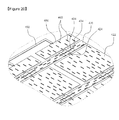
Figs. 12 to 15 , atouch panel sensor 400 according to the present embodiment comprises atransparent substrate 410,first electrode patterns 420 andsecond electrode patterns 430 formed on thesubstrate 410, and insulatingpatterns 440 interposed between thefirst electrode patterns 420 and thesecond electrode patterns 430. - The
substrate 410 may be formed using synthetic film, such as PET, PC, PE and the like, and glass substrate. Thesubstrate 410 may be installed on the display like LCD or LED display module, otherwise may be applied directly to a transparent sheet or film composing the LCD or LED display module. In this specification, the transparency of thetransparent substrate 410 can mean little opaque state only not to prevent display function, besides perfectly clear state. - The
first electrode patterns 420 and thesecond electrode patterns 430 may be formed one or both of the top side and bottom side of thesubstate 410. For example, in case of synthetic film the both electrode patterns may be formed on a top side of the film, however, in case of glass substrate they may be formed on a bottom side of the glass substrate. - The
first electrode patterns 420 may be formed using transparent conductive material, such as ITO, IZO or carbon nano tube (CNT), and may be provided in a shape of line patterns arranged parallel on thesubstrate 410, horizontally or vertically. For example, thefirst electrode patterns 420 may includeenlarged portions 422 andbridge portions 424 provided alternately in series. Theenlarged portions 422 and thebridge portions 424 aligned alternately in one row, may be formed using the same or different material. - The
enlarged portions 422 have a width relatively or considerably wider than thebridge portions 424, and thebridge portions 424 is located between everyenlarged portions 422 to electrically connect theenlarged portions 422. - For example, in a device having about 3.0 inch display and touch area, the
bridge portions 424 may be formed with a width of about 0.1∼0.2mm and theenlarged portions 422 may be formed with a width of about 4∼6mm. In this instance, theenlarged portions 422 have a width of about 20∼60 times wider than thebridge portions 424. - The
enlarged portions 422 and thebridge portions 424, as shown in drawings, may be formed in rectangular shape, otherwise may be formed in diamond, circle or oval. Theenlarged portions 422 and thebridge portions 424 may be formed with the same material or on the same surface together withtransparent connections 436, and may be formed in a various shape only to be electrically separated from each other. In a device, the display under thetouch panel sensor 400 can generate electromagnetic interference (EMI), but if theelectrode patterns transparent connections 436 are separated by minimum distance, they can reduce the EMI. - The
second electrode patterns 430 may partially overlay thefirst electrode patterns 420. Thesecond electrode patterns 430 may be formed over or under thefirst electrode patterns 420 to be electrically separated from thefirst electrode patterns 420. To separate them, an insulating layer or insulatingpatterns 440 may be formed between the first and thesecond electrode patterns - The insulating
patterns 440 may be formed using insulating material, such as SiO2, Si3N4 or TiO2, and may be formed by vaporization, sputtering, applying, spraying, laminating, adhesion, printing and the like. As shown in drawings, the insulatingpatterns 440 may be provided indirectly by patterning process after vaporization or sputtering, otherwise, may be provided directly by printing without patterning. The insulatingpatterns 440 may be provided as one insulating layer. As shown inFig. 14 , after theenlarged portions 422, thebridge portions 424 and thetransparent connections 436 are patterned, the insulatingpatterns 440 may be formed by another patterning process. - The
second electrode patterns 430 include thetransparent connections 436 and a low-resistline 434. Thetransparent connections 436 may be formed with thefirst electrode patterns 420 simultaneously. Thetransparent connections 436 may be formed with transparent conductive material to have a width of about 0.1∼0.2mm, which can be formed by photoresist process etching ITO layer, together with theenlarged portions 422 and thebridge portions 424. - As shown in
Fig. 15 , the low-resistline 434 is formed on the insulatingpatterns 440, and passes top surfaces of thetransparent connections 436 to electrically connect thetransparent connections 436. The low-resistline 434 may be formed using metal like gold, silver, aluminum or chrome, or may be formed by patterning process after vaporization or sputtering, or may be formed by printing process like silkscreen or inkjet. The low-resistline 434 may be formed with a width less than about 30µm, preferably less than about 10µm, not to be seen by unaided eye. - The low-resist
line 434 may be formed in a shape of a straight line, otherwise may be formed in a shape of a curved line or a folded line, may be changed regularly or irregularly. In case that the low-resistline 434 is formed in a shape of a irregularly curved or folded line, it cannot be seen from outside. - The low-resist
line 434 may be formed together withwire patterns 450 located at bezel area. Thewire patterns 450 of the bezel area are focused on one side of thetransparent substrate 410 to be connected to FPCB. Since thewire patterns 450 are formed with metal, it can be formed simultaneously with the low-resistline 434. -
Fig. 16 is a sectional view illustrating an overlaid structure of the touch panel sensor ofFig. 12 . - Referring to
Fig. 16 , the low-resistline 434 formed with metal is provided on thetransparent substrate 410, thebridge portions 424 and the insulatingpatterns 440. - For reference, since the transparent conductive material like ITO has an area resistance of about 250Ω/square, the transparent material of a width of about 100∼300µm and a length of about 6∼8cm may have a resistance of several hundred ohm. Thus conventional ITO electrodes are not proper to a large scale display because of extremely high resistance. However, since the metallic low-resist
line 434 is formed with metal, it can reduce the total resistance of thesecond electrode patterns 430, to improve the sensor's sensitivity. - In normal state that the finger does not approach to the touch screen, the normal capacitance may be decided by the intersection area of the
bridge portion 424 and the low-resistline 434. For reference, in conventional touch panel sensor using only ITO electrodes, between ITO films is interposed an optical clearance adhesive (OCA) film having a thickness of about 200µm to form a capacitance. However, thebridge portions 424 and the low-resistline 434 are separated by a gap of about 0.1∼1.0µm through the insulatingpatterns 440, so as to form a capacitance of about 200∼1000 times larger than the conventional touch panel sensor. By controlling the cross area of thebridge portion 424 and the low-resistline 434, the normal capacitance may be properly selected. - Since cross area of the
bridge portions 424 and the low-resistline 434 is relatively small, thesecond electrode patterns 430 may be located below thefirst electrode patterns 420. - Moreover, the low-resist
line 434 may have less resistance by increasing its thickness, with taking no effect to transparency of the touch screen. Namely, the low-resist line of this embodiment can control the resistance freely without damaging transparency and clearance. - The low-resist
line 434 of this embodiment is shaped of a straight line, however, it can be shaped of regularly or irregularly curved line or folded line not to be seen by unaided eye. - The low-resist
line 434 may further have optical absorption. In case of forming a minute dark or anti-reflection pattern on the low-resistline 434, for example with carbon/titanium (Cu/Ti), molybdenum (Mo), chrome (Cr), black chrome and the like. Otherwise, the low-resist line itself may be made of dark metal, such as Cu/Ti, Mo, Cr and the like. - According to the present embodiment, the low-resist
line 434 is formed on a top side of thefirst electrode patterns 420 and thetransparent connections 436, alternatively the low-resist line may be formed on a bottom side of them. -
Fig. 17 is a plane view illustrating a touch panel sensor according to the fifth embodiment of this invention. - Referring to
Fig. 17 , atouch panel sensor 500 according to this embodiment comprises atransparent substrate 510,first electrode patterns 520 andsecond electrode patterns 530 formed on thesubstrate 510, and insulatingpatterns 540 interposed between thefirst electrode patterns 520 and thesecond electrode patterns 530. - The
transparent substrate 510 may be formed using synthetic film or glass substrate, thefirst electrode patterns 520 includeenlarged portion 522 andbridge portions 524, and thesecond electrode patterns 530 include a low-resistline 534 andtransparent connections 536. Other descriptions for materials, structures and manufacturing can refer the descriptions and the drawings for previous embodiments. - The
second electrode patterns 530 include the low-resistline 534 and thetransparent connections 536, which are aligned in one row. In this embodiment, two or more low-resistlines 534 are grouped to form an electrode, in which top or bottom ends of the low-resist lines are electrically connected. For example, 3 low-resist lines form a group to serve as an independent low-resist line. The low-resistlines 434 ofFig. 12 are arranged by a distance of about 5mm, however, the low-resistlines 534 of this embodiment are arranged by a distance of about 1.7∼1.0mm, such that three of thelines 534 are electrically connected at top and bottom ends. - Two or more of the low-resist
lines 534 are grouped to help a instant calculation of the finger's precise position. The pattern lines are parallel connected, and each of the low-resistlines 534 in the same group is separated enough, so at to improve the sensitivity according to the changing of the capacitance. -
Fig. 18 is a plane view illustrating a touch panel sensor according to the sixth embodiment of this invention. - Referring to
Fig. 18 , atouch panel sensor 600 according to this embodiment comprises atransparent substrate 610,first electrode patterns 620 andsecond electrode patterns 630 formed on thesubstrate 610, and insulatingpatterns 640 interposed between thefirst electrode patterns 620 and thesecond electrode patterns 630. - The
transparent substrate 610 may be formed using synthetic film or glass substrate, thefirst electrode patterns 620 includeenlarged portion 622 andbridge portions 624, and thesecond electrode patterns 630 include a low-resistline 634 andtransparent connections 636. Other descriptions for materials, structures and manufacturing can refer the descriptions and the drawings for previous embodiments. - As shown in
Fig. 18 , theenlarged portions 622 are formed in a shape of circle or oval, and thetransparent connections 636 are formed in a shape having concave sides corresponding to theenlarged portions 622. The low-resistline 634 may be formed is a shape of irregularly folded line on thetransparent connections 636. - The
first electrode patterns 620 and thetransparent connections 636 are shaped for mutual harmony to be separated by minimum distance, such that they can reduce electromagnetic interference (EMI) and improve the sensitivity of the sensor. -
Fig. 19 is a partially enlarged perspective view illustrating a touch panel sensor according to the seventh embodiment of this invention. - Referring to
Fig. 19 , the touch panel sensor of this embodiment further comprises low-resistpatterns 460 formed on or in thefirst electrode patterns 420. The low-resistpatterns 460 may be formedenlarged portions 422 orbridge portions 424, and may be formed using conductive material having a low resistance less than transparent conductive material like ITO. In this embodiment, the low-resistlines 434 and the low-resistpatterns 460 may be formed using the same metal. - The low-resist
patterns 460 may be formed horizontally along thefirst electrode patterns 420, so at to reduce total resistance of thefirst electrode patterns 420. The low-resistpatterns 460 may be formed to have a thickness of less than 100Å to permit light to pass through itself. - The low-resist
patterns 460 may be formed in a shape of a straight line, otherwise, may be formed in a shape of repeatedly curved or folded line, regularly or irregularly. -
Fig. 20 is a partially enlarged perspective view illustrating a touch panel sensor according to the eighth embodiment of this invention. - Referring to
Fig. 20 , the touch panel sensor of this embodiment further comprises low-resistpatterns 465 arranged discontinuously on thefirst electrode patterns 420. The discontinuous low-resistpatterns 465 may be formed on theenlarged portions 422 or thebridge portions 424, using conductive material having a low resistance less than transparent conductive material like ITO. Contrary to the low-resistpattern 460 ofFig. 19 , the low-resistpatterns 465 of this embodiment may be formed wholly or partially on a top or bottom side of thefirst electrode patterns 420. - The low-resist
patterns 465 may be formed parallel to thefirst electrode patterns 420, otherwise may be formed irregularly. The low-resist line 434-1 may be formed on the transparent connections discontinuously. - The low-resist
patterns 465 and the low-resist lines 434-1 may work to reduce total resistance of thefirst electrode patterns 420 and thetransparent connections 436, to be arranged or scattered on the low-resistmembers 465 and 434-1. Preferably, ends of each of the low-resistpatterns 465 may be partially overlapped. - The discontinuously provided low-resist
patterns 465 and low-resist lines 434-1 may be arranged regularly, however, according to the present embodiment, they may be provided irregularly for invisibility. - As the above mentioned, however the explanation refers to desirable exemplary embodiment of this invention, present invention may be comprehended to be modified and changed within the idea and domain of this invention reported in the claims to expert dealer in this technology.
- The touch panel sensor of this invention can be used to a display module to sense a contact position of part of body.
Claims (19)
- A touch panel sensor for sensing a contact position of part of body comprising:a substrate;a resist electrode part including resist electrodes formed on the substrate to have a capacitance changeable according to approaching of the part of body; anda signal electrode part including signal electrodes formed on the resist electrode having resistance coefficient less than the resist electrode.
- The touch panel sensor of claim 1, wherein the signal electrodes are made of metal.
- The touch panel sensor of claim 1, wherein the resist electrodes are made of transparent conductive material.
- The touch panel sensor of claim 1, wherein the signal electrodes have a width less than the resist electrodes.
- The touch panel sensor of claim 1, wherein the resist electrode part comprises first electrode patterns provided parallel on one surface of the substrate, and second electrode patterns provided perpendicular to the first electrode patterns on the same surface of the substrate, to be electrically separated from the first electrodes, The second electrode patterns having transparent connections formed separated from the first electrode patterns,
the signal electrode part comprises a low-resist line formed on the transparent connections arranged in series, such that the low-resist line decreases the resistance of the second electrode patterns. - The touch panel sensor of claim 5, wherein insulating layer or insulating patterns are formed between the first electrode patterns and the signal electrode part to electrically separate the first electrode patterns and the signal electrode part.
- The touch panel sensor of claim 5, wherein the first electrode patterns include enlarged portions arranged in one row and bridge portions connecting the enlarged portions between the enlarged portions.
- The touch panel sensor of claim 7, wherein the bridge portions are overlaid over or under the low-resist line.
- The touch panel sensor of claim 1, wherein the signal electrode part is formed in a shape of a straight line, a regularly or irregularly curved line, or a regularly or irregularly folded line.
- The touch panel sensor of claim 1, the signal electrode part is provided on the resist electrode part, to have discontinuously interrupted electrode lines.
- The touch panel sensor of claim 10, the signal electrode part is formed irregularly.
- The touch panel sensor of claim 1, an optical absorption is formed on a top surface of the signal electrode part.
- The touch panel sensor of claim 1, wherein two or more of the signal electrodes are electrically connected to form a group.
- The touch panel sensor of claim 1, wherein the resist electrodes are arranged in one row on the substrate,
each of the resist electrodes has a first nod pattern and a second nod pattern mutually adjacent but electrically separated,
the resistance ratio between the first nod pattern and the second nod pattern in one of the resist electrodes is different from that in neighboring another resist electrode. - The touch panel sensor of claim 14, wherein the first nod pattern in one of the resist electrodes is electrically connected to another first nod pattern in neighboring another resist electrode, the area or the thickness of the first nod patterns increasing in order, and
the second nod pattern in the one of the resist electrodes is electrically connected to another second nod pattern in the neighboring another resist electrode, the area or the thickness of the second nod patterns decreasing in order. - The touch panel sensor of claim 1, wherein the resist electrodes are provided parallel on the substrate, each of the resist electrodes having a gradually changing width.
- A method of manufacturing a touch panel sensor for sensing a contact position of part of body comprising:providing a resist electrode part including resist electrodes formed on a substrate to have a capacitance changeable according to approaching of the part of body; andproviding a signal electrode part including signal electrodes formed above the resist electrode having resistance coefficient less than the resist electrodes.
- The method of claim 17, wherein the signal electrode part is provided using metal.
- The method of claim 17, wherein the resist electrode part is provided using transparent conductive material.
Applications Claiming Priority (3)
| Application Number | Priority Date | Filing Date | Title |
|---|---|---|---|
| KR1020090018303A KR100944519B1 (en) | 2009-03-04 | 2009-03-04 | Touch panel sensor |
| KR1020100015268A KR101128669B1 (en) | 2010-02-19 | 2010-02-19 | Touch panel sensor including low resistant line pattern |
| PCT/KR2010/001310 WO2010101399A2 (en) | 2009-03-04 | 2010-03-03 | Touch panel sensor |
Publications (2)
| Publication Number | Publication Date |
|---|---|
| EP2405328A2 true EP2405328A2 (en) | 2012-01-11 |
| EP2405328A4 EP2405328A4 (en) | 2013-10-02 |
Family
ID=42710109
Family Applications (1)
| Application Number | Title | Priority Date | Filing Date |
|---|---|---|---|
| EP10748941.1A Withdrawn EP2405328A4 (en) | 2009-03-04 | 2010-03-03 | Touch panel sensor |
Country Status (5)
| Country | Link |
|---|---|
| US (1) | US8550991B2 (en) |
| EP (1) | EP2405328A4 (en) |
| JP (1) | JP5591834B2 (en) |
| CN (1) | CN102362245A (en) |
| WO (1) | WO2010101399A2 (en) |
Cited By (7)
| Publication number | Priority date | Publication date | Assignee | Title |
|---|---|---|---|---|
| WO2012101448A3 (en) * | 2011-01-28 | 2012-11-08 | Novalia Ltd | Conductive element |
| DE102011122110A1 (en) * | 2011-12-22 | 2013-06-27 | Polyic Gmbh & Co. Kg | Operating device with display device and touch panel device, as well as multi-layer body to provide a touchpad functionality |
| DE102012112445A1 (en) * | 2012-12-17 | 2014-06-18 | Polyic Gmbh & Co. Kg | Multilayered structure for palpation field device used with e.g. mobile phone, has touch pad portions whose distance differ with respect to other touch pad portions by the ratio of corresponding touch fields of respective partial areas |
| WO2015088110A1 (en) * | 2013-12-13 | 2015-06-18 | Samsung Electronics Co., Ltd. | Method for fabricating touch panel, touch panel, and electronic device having the touch panel |
| WO2015200671A1 (en) * | 2014-06-26 | 2015-12-30 | Microchip Technology Incorporated | Compensation of a target object's coupling to feeding lines in capacitive sensing system |
| EP2873999A4 (en) * | 2012-06-29 | 2016-06-08 | Shanghai Tianma Micro Elect Co | Capacitive liquid crystal display touch panel |
| US9921698B2 (en) | 2013-05-06 | 2018-03-20 | Polyic Gmbh & Co. Kg | Layer electrode for touchscreens |
Families Citing this family (46)
| Publication number | Priority date | Publication date | Assignee | Title |
|---|---|---|---|---|
| TWI456443B (en) * | 2010-06-07 | 2014-10-11 | Wintek Corp | Touch-sensitive device and touch-sensitive display device |
| EP2584437A2 (en) * | 2010-06-16 | 2013-04-24 | Samwon St | Touch panel sensor |
| CN101950229B (en) * | 2010-09-21 | 2012-06-20 | 南京点面光电有限公司 | Resistance determining method for capacitive touch screen sensor in diamond structure |
| JP2012079169A (en) * | 2010-10-04 | 2012-04-19 | Shin Etsu Polymer Co Ltd | Detection substrate and manufacturing method for the same |
| US8822865B2 (en) | 2010-12-29 | 2014-09-02 | Lg Chem, Ltd. | Touch screen and method for manufacturing the same |
| TWI459252B (en) * | 2011-01-11 | 2014-11-01 | Hong Da Liu | Touch-type inductive device and conductive electrode structure |
| KR101129353B1 (en) * | 2011-01-31 | 2012-03-26 | 엘지이노텍 주식회사 | Touch window obtaining coordinate position on boundary portion of view area |
| US8988086B1 (en) | 2011-08-10 | 2015-03-24 | Cypress Semiconductor Corporation | Capacitive sensor array with pattern variation |
| TWI465993B (en) * | 2011-10-07 | 2014-12-21 | Rtr Tech Technology Co Ltd | Touch sensing structure and manufacturing method thereof |
| CN103164058B (en) * | 2011-12-09 | 2016-02-17 | 上海天马微电子有限公司 | Touch screen, color filter substrate and liquid crystal display |
| KR20130069938A (en) | 2011-12-19 | 2013-06-27 | 엘지이노텍 주식회사 | Conductive pattern of touch panel |
| TWI485585B (en) * | 2012-02-17 | 2015-05-21 | Innocom Tech Shenzhen Co Ltd | Composite layer structure and touch display device having the same thereof |
| JP5734504B2 (en) * | 2012-03-06 | 2015-06-17 | 三菱電機株式会社 | Touch screen, touch panel, display device and electronic device |
| US20140293168A1 (en) * | 2012-06-06 | 2014-10-02 | Wintek Corporation | Touch panel |
| KR101420330B1 (en) * | 2012-06-22 | 2014-07-16 | 삼성디스플레이 주식회사 | Flexible display apparatus |
| TWI472997B (en) * | 2012-08-16 | 2015-02-11 | Yomore Technology Co Ltd | Touch panel system and fabrication method of a touch panel system |
| US9389737B2 (en) | 2012-09-14 | 2016-07-12 | Samsung Display Co., Ltd. | Display device and method of driving the same in two modes |
| US11314368B2 (en) | 2012-09-14 | 2022-04-26 | Samsung Display Co., Ltd. | Display device and method of driving the same in two modes |
| TWI483165B (en) | 2012-09-21 | 2015-05-01 | Au Optronics Corp | Capacitive touch sensor structure and applications thereof |
| KR102119791B1 (en) | 2012-09-27 | 2020-06-05 | 엘지이노텍 주식회사 | Touch panel |
| KR102009880B1 (en) * | 2012-10-23 | 2019-08-12 | 엘지디스플레이 주식회사 | Metal mesh type touch screen panel |
| CN103793089B (en) * | 2012-10-30 | 2017-05-17 | 宸鸿科技(厦门)有限公司 | Touch panel |
| KR102040973B1 (en) | 2012-12-14 | 2019-11-06 | 삼성디스플레이 주식회사 | Touch Screen Panel |
| WO2014113983A1 (en) | 2013-01-28 | 2014-07-31 | Texas Instruments Incorporated | Capacitive single layer multi-touch panel having improved response characteristics |
| KR102075040B1 (en) | 2013-02-05 | 2020-02-11 | 삼성디스플레이 주식회사 | Touch Screen Panel |
| CN103176650B (en) * | 2013-03-01 | 2016-09-28 | 南昌欧菲光科技有限公司 | Conducting glass substrate and preparation method thereof |
| US9645695B2 (en) | 2013-03-07 | 2017-05-09 | Mitsubishi Electric Corporation | Display apparatus |
| US9594462B2 (en) | 2013-04-22 | 2017-03-14 | Cypress Semiconductor Corporation | Uniform signals from non-uniform patterns of electrodes |
| TW201443725A (en) * | 2013-05-13 | 2014-11-16 | Hon Hai Prec Ind Co Ltd | Touch screen and method of manufacturing the same |
| TWM476988U (en) * | 2013-11-22 | 2014-04-21 | Wintek Corp | Touch panel |
| WO2015112419A1 (en) * | 2014-01-23 | 2015-07-30 | 3M Innovative Properties Company | Method for patterning a microstructure |
| US10234980B2 (en) * | 2014-03-11 | 2019-03-19 | Lg Innotek Co., Ltd. | Touch window |
| KR102275892B1 (en) * | 2014-03-11 | 2021-07-12 | 엘지이노텍 주식회사 | Touch panel |
| TWI502445B (en) * | 2014-06-11 | 2015-10-01 | Innolux Corp | Touch display device and touch substrate |
| KR102195039B1 (en) * | 2014-07-02 | 2020-12-24 | 동우 화인켐 주식회사 | Electrode structure for touch panel and method for fabricating the same |
| US20200310584A1 (en) * | 2016-03-30 | 2020-10-01 | Fujikura Ltd. | Wiring body, wiring board, and touch sensor |
| CN105867689B (en) * | 2016-04-07 | 2018-06-05 | 京东方科技集团股份有限公司 | A kind of production method of touch display substrate and the array substrate of touch control display apparatus |
| JP6369589B1 (en) * | 2017-03-30 | 2018-08-08 | Smk株式会社 | Capacitive touch panel |
| CN107463296B (en) * | 2017-09-21 | 2024-03-29 | 京东方科技集团股份有限公司 | Display panel, touch screen and display device |
| KR102079389B1 (en) * | 2017-09-29 | 2020-02-19 | 주식회사 센트론 | Display using passive matrix organic light emitting diode |
| JP2019067143A (en) * | 2017-09-29 | 2019-04-25 | 株式会社ジャパンディスプレイ | Detector and display |
| JP2019219882A (en) * | 2018-06-19 | 2019-12-26 | 洋華光電股▲ふん▼有限公司 | Transparent conductive film and method for reducing local resistance value in product thereof |
| KR102604474B1 (en) | 2019-03-12 | 2023-11-22 | 삼성전자주식회사 | Electronic device including antenna device |
| DE112020004388T5 (en) | 2019-09-18 | 2022-06-02 | Alps Alpine Co., Ltd. | Electrostatic capacitance sensor and input device |
| CN114816134B (en) * | 2021-01-29 | 2024-05-28 | 宸美(厦门)光电有限公司 | Touch sensor and manufacturing method thereof |
| US11474649B2 (en) | 2021-03-05 | 2022-10-18 | Tpk Advanced Solutions Inc. | Touch sensor and manufacturing method thereof |
Citations (5)
| Publication number | Priority date | Publication date | Assignee | Title |
|---|---|---|---|---|
| WO2005114369A2 (en) * | 2004-05-06 | 2005-12-01 | Apple Computer, Inc. | Multipoint touchscreen |
| EP1798778A2 (en) * | 2005-12-14 | 2007-06-20 | Korea Advanced Institute of Science and Technology | Integrated thin-film solar cell and method of manufacturing the same |
| US20080259044A1 (en) * | 2007-04-20 | 2008-10-23 | Seiko Epson Corporation | Coordinate input device and display device |
| US20080277259A1 (en) * | 2007-05-11 | 2008-11-13 | Sense Pad Tech Co., Ltd | Capacitive type touch panel |
| US20090002337A1 (en) * | 2007-06-28 | 2009-01-01 | Sense Pad Tech Co., Ltd | Capacitive-type touch panel |
Family Cites Families (25)
| Publication number | Priority date | Publication date | Assignee | Title |
|---|---|---|---|---|
| DE69324067T2 (en) * | 1992-06-08 | 1999-07-15 | Synaptics Inc | Object position detector |
| KR101192391B1 (en) | 2005-05-26 | 2012-10-17 | 군제 가부시키가이샤 | Transparent planar body and transparent touch switch |
| TWI267773B (en) | 2005-05-31 | 2006-12-01 | Wintek Corp | Manufacturing method of a touch panel |
| JP4610416B2 (en) * | 2005-06-10 | 2011-01-12 | 日本写真印刷株式会社 | Capacitive touch panel |
| ES2318382T3 (en) | 2005-06-16 | 2009-05-01 | Asulab S.A. | MANUFACTURING PROCEDURE OF A TRANSPARENT ELEMENT THAT INCLUDES TRANSPARENT ELECTRODES AND CORRESPONDING ELEMENT. |
| TW200805128A (en) * | 2006-05-05 | 2008-01-16 | Harald Philipp | Touch screen element |
| JP2008233976A (en) | 2007-03-16 | 2008-10-02 | Sharp Corp | Touch panel, display device, and manufacturing method for touch panel |
| JP5123931B2 (en) | 2007-03-27 | 2013-01-23 | 京セラ株式会社 | Touch panel and touch panel display device |
| US20080309633A1 (en) | 2007-06-13 | 2008-12-18 | Apple Inc. | Touch-sensitive display |
| KR100909264B1 (en) * | 2007-06-14 | 2009-07-27 | 주식회사 애니텍 | Capacitive touch panel and keypad integrated communication terminal device including the same |
| JP4984289B2 (en) * | 2007-06-21 | 2012-07-25 | 関西電力株式会社 | COMMUNICATION SYSTEM, COMMUNICATION METHOD, AND COMMUNICATION DEVICE |
| JP2009009249A (en) * | 2007-06-26 | 2009-01-15 | Nissha Printing Co Ltd | Capacitance type touch panel and two system combined use touch panel using the same |
| TW200921483A (en) | 2007-11-09 | 2009-05-16 | Tpk Touch Solutions Inc | Touch-control display panel with an electric-field shielding layer |
| KR100979910B1 (en) | 2008-01-29 | 2010-09-06 | (주)멜파스 | Touchscreen panel having partitioned transparent electrode structure |
| TWM343210U (en) | 2008-05-30 | 2008-10-21 | Tpk Touch Solutions Inc | Display panel integrating the touch-control structure |
| JP4720857B2 (en) | 2008-06-18 | 2011-07-13 | ソニー株式会社 | Capacitance type input device and display device with input function |
| KR20100006987A (en) | 2008-07-11 | 2010-01-22 | 삼성모바일디스플레이주식회사 | Touch screen panel and fabricating method for the same |
| KR101048980B1 (en) | 2009-01-16 | 2011-07-12 | 삼성모바일디스플레이주식회사 | Touch screen panel and its manufacturing method |
| CN101847065B (en) * | 2009-03-24 | 2013-01-23 | 宸鸿科技(厦门)有限公司 | Circuit structure of capacitance type touch control panel |
| JP2010231533A (en) * | 2009-03-27 | 2010-10-14 | Citizen Electronics Co Ltd | Transparent electrode substrate and touch panel provided therewith |
| KR100954894B1 (en) | 2009-09-10 | 2010-04-28 | 남동식 | Touch panel sensor |
| KR101073684B1 (en) | 2009-08-25 | 2011-10-14 | 주식회사 지니틱스 | Transparent Electrode Pattern Of Capacitive Touch Screen For Low Resistance |
| KR100962047B1 (en) | 2009-09-28 | 2010-06-08 | 남동식 | Touch panel sensor with transparent electrodes in groups |
| TWM410924U (en) * | 2011-02-08 | 2011-09-01 | Derlead Invest Ltd | Projection-type capacitance touch panel with sensitivity adjustment structure |
| US20120218028A1 (en) * | 2011-02-28 | 2012-08-30 | Tpk Touch Solutions Inc. | Capacitive touch panel, touch sensor structure and a method for manufacturing the capacitive touch panel |
-
2010
- 2010-03-03 EP EP10748941.1A patent/EP2405328A4/en not_active Withdrawn
- 2010-03-03 US US13/254,807 patent/US8550991B2/en not_active Expired - Fee Related
- 2010-03-03 CN CN2010800105056A patent/CN102362245A/en active Pending
- 2010-03-03 WO PCT/KR2010/001310 patent/WO2010101399A2/en active Application Filing
- 2010-03-03 JP JP2011552884A patent/JP5591834B2/en not_active Expired - Fee Related
Patent Citations (5)
| Publication number | Priority date | Publication date | Assignee | Title |
|---|---|---|---|---|
| WO2005114369A2 (en) * | 2004-05-06 | 2005-12-01 | Apple Computer, Inc. | Multipoint touchscreen |
| EP1798778A2 (en) * | 2005-12-14 | 2007-06-20 | Korea Advanced Institute of Science and Technology | Integrated thin-film solar cell and method of manufacturing the same |
| US20080259044A1 (en) * | 2007-04-20 | 2008-10-23 | Seiko Epson Corporation | Coordinate input device and display device |
| US20080277259A1 (en) * | 2007-05-11 | 2008-11-13 | Sense Pad Tech Co., Ltd | Capacitive type touch panel |
| US20090002337A1 (en) * | 2007-06-28 | 2009-01-01 | Sense Pad Tech Co., Ltd | Capacitive-type touch panel |
Non-Patent Citations (1)
| Title |
|---|
| See also references of WO2010101399A2 * |
Cited By (13)
| Publication number | Priority date | Publication date | Assignee | Title |
|---|---|---|---|---|
| WO2012101448A3 (en) * | 2011-01-28 | 2012-11-08 | Novalia Ltd | Conductive element |
| US9425790B2 (en) | 2011-01-28 | 2016-08-23 | Novalia Ltd. | Conductive element |
| US9465465B2 (en) | 2011-12-22 | 2016-10-11 | Polyic Gmbh & Co. Kg | Multilayer body forming display apparatus touchpad |
| DE102011122110A1 (en) * | 2011-12-22 | 2013-06-27 | Polyic Gmbh & Co. Kg | Operating device with display device and touch panel device, as well as multi-layer body to provide a touchpad functionality |
| DE102011122110B4 (en) | 2011-12-22 | 2023-05-25 | Polyic Gmbh & Co. Kg | Operating device with display device and touch panel device, and multi-layer body for providing a touch panel functionality |
| EP2873999A4 (en) * | 2012-06-29 | 2016-06-08 | Shanghai Tianma Micro Elect Co | Capacitive liquid crystal display touch panel |
| DE102012112445A1 (en) * | 2012-12-17 | 2014-06-18 | Polyic Gmbh & Co. Kg | Multilayered structure for palpation field device used with e.g. mobile phone, has touch pad portions whose distance differ with respect to other touch pad portions by the ratio of corresponding touch fields of respective partial areas |
| US9921698B2 (en) | 2013-05-06 | 2018-03-20 | Polyic Gmbh & Co. Kg | Layer electrode for touchscreens |
| WO2015088110A1 (en) * | 2013-12-13 | 2015-06-18 | Samsung Electronics Co., Ltd. | Method for fabricating touch panel, touch panel, and electronic device having the touch panel |
| US9461645B2 (en) | 2013-12-13 | 2016-10-04 | Samsung Electronics Co., Ltd. | Method for fabricating touch panel, touch panel, and electronic device having the touch panel |
| US9671920B2 (en) | 2014-06-26 | 2017-06-06 | Microchip Technology Incorporated | Compensation of a target object coupling to feeding lines in capacitive sensing system |
| US10345985B2 (en) | 2014-06-26 | 2019-07-09 | Microchip Technology Incorporated | Compensation of a target objects coupling to feeding lines in capacitive sensing system |
| WO2015200671A1 (en) * | 2014-06-26 | 2015-12-30 | Microchip Technology Incorporated | Compensation of a target object's coupling to feeding lines in capacitive sensing system |
Also Published As
| Publication number | Publication date |
|---|---|
| US20120056664A1 (en) | 2012-03-08 |
| US8550991B2 (en) | 2013-10-08 |
| WO2010101399A3 (en) | 2010-12-09 |
| WO2010101399A2 (en) | 2010-09-10 |
| JP2012519897A (en) | 2012-08-30 |
| EP2405328A4 (en) | 2013-10-02 |
| CN102362245A (en) | 2012-02-22 |
| JP5591834B2 (en) | 2014-09-17 |
Similar Documents
| Publication | Publication Date | Title |
|---|---|---|
| US8550991B2 (en) | Touch panel sensor | |
| KR101128669B1 (en) | Touch panel sensor including low resistant line pattern | |
| JP6336744B2 (en) | Electrode member and touch panel including the same | |
| KR101121120B1 (en) | Touch panel sensor including opaque electrode pattern | |
| US9941877B2 (en) | Electrode pattern of touch panel | |
| KR101620463B1 (en) | Electrostatic capacity type touch panel and manufacuring method thereof | |
| KR101415583B1 (en) | Touch panel and forming method for the same | |
| TWI525514B (en) | Integrated passive circuit elements for sensing devices | |
| EP2209065A2 (en) | Touch screen panel and method for fabricating the same | |
| TWI628565B (en) | Conductive sheet, electrostatic capacity type touch panel and display device | |
| CN104793783A (en) | Touch window | |
| KR100944519B1 (en) | Touch panel sensor | |
| KR20120018059A (en) | Substrate for touch screen panel, touch screen panel and fabrication method thereof | |
| KR101886279B1 (en) | Fabrication method of electrode-pattern of touch panel | |
| JPWO2019021835A1 (en) | Conductive member for touch panel and touch panel | |
| KR101370443B1 (en) | Conductive pattern of touch panel | |
| KR20140071026A (en) | Touch panel and method of fabricating the same | |
| KR102251870B1 (en) | Touch window | |
| KR101836232B1 (en) | Touch panel | |
| KR102187470B1 (en) | Touch window | |
| KR102238822B1 (en) | Touch window | |
| KR20160082042A (en) | Touch panel | |
| KR102175779B1 (en) | Electrode member and touch winow having the same | |
| KR20140030896A (en) | Touch panel sensor and method of manufacturing touch panel sensor | |
| KR102288813B1 (en) | Touch window |
Legal Events
| Date | Code | Title | Description |
|---|---|---|---|
| PUAI | Public reference made under article 153(3) epc to a published international application that has entered the european phase |
Free format text: ORIGINAL CODE: 0009012 |
|
| 17P | Request for examination filed |
Effective date: 20110929 |
|
| AK | Designated contracting states |
Kind code of ref document: A2 Designated state(s): AT BE BG CH CY CZ DE DK EE ES FI FR GB GR HR HU IE IS IT LI LT LU LV MC MK MT NL NO PL PT RO SE SI SK SM TR |
|
| DAX | Request for extension of the european patent (deleted) | ||
| A4 | Supplementary search report drawn up and despatched |
Effective date: 20130830 |
|
| RIC1 | Information provided on ipc code assigned before grant |
Ipc: G06F 3/045 20060101ALI20130826BHEP Ipc: G06F 3/044 20060101AFI20130826BHEP Ipc: H03K 17/96 20060101ALI20130826BHEP |
|
| STAA | Information on the status of an ep patent application or granted ep patent |
Free format text: STATUS: THE APPLICATION IS DEEMED TO BE WITHDRAWN |
|
| 18D | Application deemed to be withdrawn |
Effective date: 20140328 |