EP2424437B1 - Imaging apparatus and imaging system, and control method and program for the same - Google Patents
Imaging apparatus and imaging system, and control method and program for the same Download PDFInfo
- Publication number
- EP2424437B1 EP2424437B1 EP10713255.7A EP10713255A EP2424437B1 EP 2424437 B1 EP2424437 B1 EP 2424437B1 EP 10713255 A EP10713255 A EP 10713255A EP 2424437 B1 EP2424437 B1 EP 2424437B1
- Authority
- EP
- European Patent Office
- Prior art keywords
- radiation
- imaging
- detector
- irradiation
- imaging operation
- Prior art date
- Legal status (The legal status is an assumption and is not a legal conclusion. Google has not performed a legal analysis and makes no representation as to the accuracy of the status listed.)
- Not-in-force
Links
- 238000003384 imaging method Methods 0.000 title claims description 172
- 238000000034 method Methods 0.000 title claims description 10
- 230000005855 radiation Effects 0.000 claims description 124
- 238000009825 accumulation Methods 0.000 claims description 83
- 238000006243 chemical reaction Methods 0.000 claims description 68
- 239000011159 matrix material Substances 0.000 claims description 6
- 230000007246 mechanism Effects 0.000 claims description 6
- 230000001678 irradiating effect Effects 0.000 claims description 2
- 238000012545 processing Methods 0.000 description 35
- 230000008859 change Effects 0.000 description 18
- 230000010354 integration Effects 0.000 description 17
- 238000012937 correction Methods 0.000 description 13
- 239000003990 capacitor Substances 0.000 description 12
- 238000002601 radiography Methods 0.000 description 12
- 238000001514 detection method Methods 0.000 description 7
- 239000004065 semiconductor Substances 0.000 description 5
- 230000015556 catabolic process Effects 0.000 description 4
- 238000006731 degradation reaction Methods 0.000 description 4
- 230000000694 effects Effects 0.000 description 4
- 238000007689 inspection Methods 0.000 description 4
- 230000004044 response Effects 0.000 description 4
- 230000005540 biological transmission Effects 0.000 description 3
- 238000003745 diagnosis Methods 0.000 description 3
- 238000010586 diagram Methods 0.000 description 3
- 238000005070 sampling Methods 0.000 description 3
- 238000012986 modification Methods 0.000 description 2
- 230000004048 modification Effects 0.000 description 2
- 239000002245 particle Substances 0.000 description 2
- 239000000758 substrate Substances 0.000 description 2
- 206010047571 Visual impairment Diseases 0.000 description 1
- 229910021417 amorphous silicon Inorganic materials 0.000 description 1
- 230000003321 amplification Effects 0.000 description 1
- JJWKPURADFRFRB-UHFFFAOYSA-N carbonyl sulfide Chemical compound O=C=S JJWKPURADFRFRB-UHFFFAOYSA-N 0.000 description 1
- 238000013480 data collection Methods 0.000 description 1
- 230000001419 dependent effect Effects 0.000 description 1
- 230000001066 destructive effect Effects 0.000 description 1
- 239000011521 glass Substances 0.000 description 1
- 239000012535 impurity Substances 0.000 description 1
- 239000000463 material Substances 0.000 description 1
- 238000003199 nucleic acid amplification method Methods 0.000 description 1
- 230000008569 process Effects 0.000 description 1
- 230000005258 radioactive decay Effects 0.000 description 1
- 230000035945 sensitivity Effects 0.000 description 1
- 230000006641 stabilisation Effects 0.000 description 1
- 238000011105 stabilization Methods 0.000 description 1
- 239000010409 thin film Substances 0.000 description 1
Images


Classifications
-
- A—HUMAN NECESSITIES
- A61—MEDICAL OR VETERINARY SCIENCE; HYGIENE
- A61B—DIAGNOSIS; SURGERY; IDENTIFICATION
- A61B6/00—Apparatus or devices for radiation diagnosis; Apparatus or devices for radiation diagnosis combined with radiation therapy equipment
- A61B6/02—Arrangements for diagnosis sequentially in different planes; Stereoscopic radiation diagnosis
- A61B6/03—Computed tomography [CT]
- A61B6/032—Transmission computed tomography [CT]
-
- A—HUMAN NECESSITIES
- A61—MEDICAL OR VETERINARY SCIENCE; HYGIENE
- A61B—DIAGNOSIS; SURGERY; IDENTIFICATION
- A61B6/00—Apparatus or devices for radiation diagnosis; Apparatus or devices for radiation diagnosis combined with radiation therapy equipment
- A61B6/42—Arrangements for detecting radiation specially adapted for radiation diagnosis
- A61B6/4208—Arrangements for detecting radiation specially adapted for radiation diagnosis characterised by using a particular type of detector
- A61B6/4233—Arrangements for detecting radiation specially adapted for radiation diagnosis characterised by using a particular type of detector using matrix detectors
-
- A—HUMAN NECESSITIES
- A61—MEDICAL OR VETERINARY SCIENCE; HYGIENE
- A61B—DIAGNOSIS; SURGERY; IDENTIFICATION
- A61B6/00—Apparatus or devices for radiation diagnosis; Apparatus or devices for radiation diagnosis combined with radiation therapy equipment
- A61B6/58—Testing, adjusting or calibrating thereof
- A61B6/582—Calibration
- A61B6/585—Calibration of detector units
-
- G—PHYSICS
- G01—MEASURING; TESTING
- G01T—MEASUREMENT OF NUCLEAR OR X-RADIATION
- G01T1/00—Measuring X-radiation, gamma radiation, corpuscular radiation, or cosmic radiation
- G01T1/29—Measurement performed on radiation beams, e.g. position or section of the beam; Measurement of spatial distribution of radiation
- G01T1/2914—Measurement of spatial distribution of radiation
- G01T1/2921—Static instruments for imaging the distribution of radioactivity in one or two dimensions; Radio-isotope cameras
- G01T1/2928—Static instruments for imaging the distribution of radioactivity in one or two dimensions; Radio-isotope cameras using solid state detectors
-
- H—ELECTRICITY
- H04—ELECTRIC COMMUNICATION TECHNIQUE
- H04N—PICTORIAL COMMUNICATION, e.g. TELEVISION
- H04N23/00—Cameras or camera modules comprising electronic image sensors; Control thereof
- H04N23/30—Cameras or camera modules comprising electronic image sensors; Control thereof for generating image signals from X-rays
-
- H—ELECTRICITY
- H04—ELECTRIC COMMUNICATION TECHNIQUE
- H04N—PICTORIAL COMMUNICATION, e.g. TELEVISION
- H04N25/00—Circuitry of solid-state image sensors [SSIS]; Control thereof
- H04N25/60—Noise processing, e.g. detecting, correcting, reducing or removing noise
- H04N25/62—Detection or reduction of noise due to excess charges produced by the exposure, e.g. smear, blooming, ghost image, crosstalk or leakage between pixels
- H04N25/626—Reduction of noise due to residual charges remaining after image readout, e.g. to remove ghost images or afterimages
-
- H—ELECTRICITY
- H04—ELECTRIC COMMUNICATION TECHNIQUE
- H04N—PICTORIAL COMMUNICATION, e.g. TELEVISION
- H04N5/00—Details of television systems
- H04N5/30—Transforming light or analogous information into electric information
- H04N5/32—Transforming X-rays
-
- H—ELECTRICITY
- H04—ELECTRIC COMMUNICATION TECHNIQUE
- H04N—PICTORIAL COMMUNICATION, e.g. TELEVISION
- H04N25/00—Circuitry of solid-state image sensors [SSIS]; Control thereof
- H04N25/70—SSIS architectures; Circuits associated therewith
- H04N25/76—Addressed sensors, e.g. MOS or CMOS sensors
Definitions
- the present invention relates to an imaging apparatus and an imaging system, and a control method and a program for the same. More specifically, the present invention relates to a radiation imaging apparatus and a radiation imaging system, and a control method and a program for the same preferably used for still image radiographing such as radiography and moving image radiographing such as fluoroscopic imaging in medical diagnosis.
- radiation according to the present invention should include not only ⁇ radiation, ⁇ radiation, and y radiation which are beams composed of particles (including photons) released by radioactive decay but also beams having the same or more energy such as X rays, particle radiation, and cosmic rays.
- the radiation imaging apparatus As an imaging apparatus for use in medical image diagnosis and non-destructive inspection using X rays, recent years have seen the practical application of a radiation imaging apparatus using a flat panel detector (FPD) formed of semiconductor materials.
- FPD flat panel detector
- the radiation imaging apparatus has been used as a digital imaging apparatus for still image radiographing such as radiography and moving image radiographing such as fluoroscopic imaging.
- Patent Citation 1 investigates a radiation imaging apparatus capable of switching the FPD-read area (size of field of view) and the X-ray irradiation area.
- the pixel sensitivity and the output under a dark state are different between the irradiated area and the non-irradiated area of the FPD. Consequently, a ghost (step of image) affected by the irradiation area occurs in the acquired image, which may lead to degradation of image quality.
- Patent Citation 2 investigates performing image processing for correction. Specifically, a ghost correction coefficient is calculated for each X-ray irradiation condition based on ghost data obtained by uniform irradiation. The ghost correction coefficient is used to acquire a required ghost correction coefficient corresponding to the X-ray irradiation condition and the elapsed time from the start of the X-ray irradiation when data about the target portion of inspection object, which is the irradiation area, is collected. Then, correction image data is generated by correcting the data about the target portion of inspection object by the required ghost correction coefficient.
- Patent Citation 2 uses image processing for correction, and thus involves complicated parameter management and correction processing, thereby complicating the entire apparatus.
- data acquisition for correction is required in advance, leading to complicated operation.
- strict management needs to be in place for the data collection method, leading to difficult management.
- the correction technique does not reduce the after-image quantity itself which causes the above ghost and is contained in an image signal obtained from the FPD, and thus it is difficult to obtain an optimal effect under various circumstances.
- the present inventors have made zealous studies so as to provide an imaging apparatus and a system which can reduce a step of image which may occur in an obtained image and is affected by an irradiation area and can prevent remarkable degradation of image quality without performing complicated image processing.
- the inventors have envisioned the embodiments as described below.
- the present invention can reduce a ghost (step of image) which may occur in an obtained image and is affected by an irradiation area and can prevent remarkable degradation of image quality by drive operation of an FPD without performing complicated image processing.
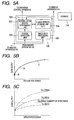
- the radiation imaging system of the present embodiment illustrated in FIG. 1 includes an imaging apparatus 100, a controlling computer 108, a radiation control apparatus 109, a radiation generating apparatus 110, a display apparatus 113, and a control console 114.
- the imaging apparatus 100 has an FPD (flat panel detector) 104 which includes a detector unit 101 having a plurality of pixels each converting radiation or light to electrical signal; a driving circuit 102 driving the detector unit 101; and a read out circuit 103 outputting an electrical signal from the driven detector unit 101 as image data.
- FPD flat panel detector
- the imaging apparatus 100 further includes a signal processing unit 105 which processes and outputs image data from the FPD 104; a controller unit 106 which controls an operation of the FPD 104 by supplying a control signal to each component; and a power source unit 107 which supplies bias to each component.
- the signal processing unit 105 which receives a control signal from the later described controlling computer 108 and provides the control signal to the controller unit 106.
- the power source unit 107 includes a power supply circuit such as a regulator which receives voltage from an external power source and a built-in battery (not illustrated) and supplies voltage required for the detector unit 101, the driving circuit 102, and the read out circuit 103.
- the controlling computer 108 performs synchronization between the radiation generating apparatus 110 and the imaging apparatus 100; transmission of a control signal for determining a state of the imaging apparatus 100; and image processing for correction, storage, and display on image data from the imaging apparatus 100.
- the controlling computer 108 transmits, to the radiation control apparatus 109, a control signal determining a radiation irradiation condition based on information from the control console 114.
- the radiation control apparatus 109 controls an operation of a radiation source 111 emitting radiation therefrom and an operation of an irradiation field aperture mechanism 112, which are included in the radiation generating apparatus 110.
- the irradiation field aperture mechanism 112 has a function capable of changing a predetermined irradiation field which is an area for irradiating the detector unit 101 of the FPD 104 with radiation or light according to radiation.
- the irradiation field aperture mechanism 112 has a function capable of switching between an irradiation field A and an irradiation field B.
- the irradiation field A corresponding to the first irradiation field of the present invention is irradiated with radiation corresponding to part of pixels contained in a plurality of pixels, assuming that, for example, the plurality of pixels is a total of pixels of about 2800 rows x about 2800 columns and the part of pixels is about 1000 rows x about 1000 columns.
- the irradiation field B corresponding to the second irradiation field of the present invention is irradiated with radiation corresponding to all the pixels wider than the irradiation field A.
- the control console 114 inputs examinee information and imaging conditions as parameters for various control of the controlling computer 108 and transmits the parameters to the controlling computer 108.
- the display apparatus 113 displays image data undergoing image processing by the controlling computer 108.
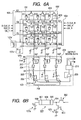
- FIG. 2 illustrates the imaging apparatus including the FPD having pixels of 3 rows ⁇ 3 columns. Note that in fact, an actual imaging apparatus has more pixels. For example, a 17-inch imaging apparatus has pixels of about 2800 rows ⁇ about 2800 columns.
- the detector unit 101 has a plurality of pixels arranged in a matrix form. Each pixel has a conversion element 201 converting radiation or light to electric charge; and a switching element 202 outputting an electrical signal according to the electric charge.
- a photoelectric conversion element converting light emitted to a conversion element to electric charge
- a PIN photodiode mainly composed of amorphous silicon arranged on an insulating substrate such as a glass substrate is used.
- the conversion element an indirect conversion element having a wavelength converter provided on a radiation incident side of the above described photoelectric conversion element, which converts radiation into light on a wavelength band sensible by the photoelectric conversion element and a direct conversion element which directly converts radiation into an electric charge are preferably used.
- the switching element 202 a transistor having a control terminal and two main terminals are preferably used. According to the present embodiment, a thin-film transistor (TFT) is used.
- One electrode of the conversion element 201 is electrically connected to one of the two main terminals of the switching element 202, and the other electrode is electrically connected to a bias power source 107a via a common bias line Bs.
- the control terminals of a plurality of switching elements in rows such as T11 to T13 are electrically connected commonly to a drive line G1 in the first row, and a drive signal for controlling a conducting state of the switching elements is provided from the driving circuit 102 in units of rows via the drive line.
- the other main terminal of the control terminals of a plurality of switching elements in columns such as T11 to T31 are electrically connected to a signal line Sig 1 in the first column and outputs an electrical signal according to the electric charge of the conversion element to the read out circuit 103 via the signal line while the switching element is in a conducting state.
- the plurality of signal lines Sig 1 to Sig 3 provided in columns transmit electrical signals outputted from a plurality of pixels to the read out circuit 103 in parallel.
- the read out circuit 103 includes an amplifier circuit 207 amplifying an electrical signal outputted in parallel from the detector unit 101, and the amplifier circuit 207 is provided for each signal line.
- Each amplifier circuit 207 includes an integration amplifier 203 amplifying an outputted electrical signal; a variable amplifier 204 amplifying the electrical signal from the integration amplifier 203; a sample hold circuit 205 sampling and holding the amplified electrical signal; and a buffer amplifier 206.
- the integration amplifier 203 includes an arithmetic amplifier amplifying and outputting the read electrical signal; an integration capacitor; and a reset switch. The integration amplifier 203 can change the amplification ratio by changing the integration capacitor value.
- the outputted electrical signal is inputted to an inverting input terminal of the arithmetic amplifier.
- a reference voltage Vref is inputted to a non-inverting input terminal from the reference power source 107b, and the amplified electrical signal is outputted from the output terminal.
- the integration capacitor is located between the inverting input terminal and the output terminal of the arithmetic amplifier.
- the sample hold circuit 205 is provided for each amplifier circuit and includes a sampling switch and a sampling capacitor.
- the read out circuit 103 includes a multiplexer 208 which sequentially outputs the electrical signal read in parallel from each amplifier circuit 207 and outputs a serial image signal; and a buffer amplifier 209 which performs impedance conversion on the image signal to be outputted.
- An image signal Vout which is an analog electrical signal outputted from the buffer amplifier 209, is converted to digital image data by the A/D converter 210 and is outputted to the signal processing unit 105.
- the image data processed by the signal processing unit 105 illustrated in FIG. 1 is outputted to the controlling computer 108.
- the driving circuit 102 In response to the control signals (D-CLK, OE, and DIO) inputted from the controller unit 106 illustrated in FIG. 1 , the driving circuit 102 outputs, to each drive line, the drive signal having a conducting voltage Vcom for placing the switching element in a conducting state and a non-conducting voltage Vss for placing the switching element to a non-conducting state. Thereby, the driving circuit 102 controls the conducting state and the non-conducting state of the switching element and drives the detector unit 101.
- the control signals D-CLK, OE, and DIO
- the power source unit 107 illustrated in FIG. 1 includes the bias power source 107a and the reference power source 107b of the amplifier circuit illustrated in FIG. 2 .
- the bias power source 107a supplies a bias voltage Vs commonly to the other electrode of each conversion element via the bias line Bs.
- the bias voltage Vs corresponds to the first voltage of the present invention.
- the reference power source 107b supplies a reference voltage Vref to a non-inverting input terminal of each arithmetic amplifier.
- the controller unit 106 illustrated in FIG. 1 receives control signals from the controlling computer 108 and other external devices via the signal processing unit 105 and controls the operation of the FPD 104 by giving various control signals to the driving circuit 102, the power source unit 107, and the read out circuit 103.
- the controller unit 106 controls the operation of the driving circuit 102 by providing the driving circuit 102 with the control signal D-CLK, the control signal OE, and the control signal DIO.
- the control signal D-CLK is a shift clock for a shift register used as the driving circuit
- the control signal DIO is a pulse transferred by the shift register
- the control signal OE is a control signal for controlling an output end of the shift register.
- the controller unit 106 controls the operation of various components of the read out circuit 103 by providing the read out circuit 103 with a control signal RC, a control signal SH, and a control signal CLK.
- the control signal RC is a control signal for controlling the operation of the reset switch of the integration amplifier
- the control signal SH is a control signal for controlling the operation of the sample hold circuit 205
- the control signal CLK is a control signal for controlling the operation of the multiplexer 208.
- FIGS. 1 to 3 particularly FIG. 3
- the operator operates the control console 114; the controlling computer 108 determines the irradiation conditions; and imaging starts.
- a desired dose of radiation is delivered to an examinee from the radiation generating apparatus 110 controlled by the radiation control apparatus 109 under the irradiation conditions.
- the imaging apparatus 100 outputs image data according to the radiation transmitted through the examinee.
- the outputted image data undergoes image processing by the controlling computer 108 and is displayed on the display apparatus 113.
- the controlling computer 108 prompts the operator to confirm whether or not to continue imaging. If an instruction of no imaging continuation (NO) is received from the operator, the controlling computer 108 terminates imaging; and if an instruction of imaging continuation (YES) is received from the operator, the controlling computer 108 prompts the operator to confirm whether or not to change the irradiation field. If an instruction of no irradiation field change (NO) is received from the operator, the controlling computer 108 controls the radiation control apparatus 109 and the radiation generating apparatus 110 under the previously determined imaging conditions so that radiation is delivered again under the same conditions. Conversely, if an instruction of irradiation field change (YES) is received from the operator, the controlling computer 108 determines the irradiation conditions where the irradiation field is changed.
- NO no imaging continuation
- YES instruction of imaging continuation
- the radiation control apparatus 109 controls the irradiation field aperture mechanism 112 of the radiation generating apparatus 110 so as to determine the changed irradiation field.
- the controlling computer 108 performs an arithmetic processing for determining an accumulation period described in detail later. Subsequently, the controlling computer 108 controls the radiation control apparatus 109 and the radiation generating apparatus 110 under the irradiation conditions including the irradiation field determined by the controlling computer 108 and the irradiation time according to the accumulation period so as to deliver radiation under the changed irradiation conditions.
- the controlling computer 108 provides the imaging apparatus 100 with the control signal based on the determined accumulation period and the next imaging is performed under the determined accumulation period.
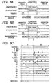
- the imaging apparatus 100 when the bias voltage Vs is supplied to the conversion element 201, the imaging apparatus 100 performs an idling operation in the idling period.
- the idling operation means an operation for repeatedly performing at least an initialization operation K1 a plurality of times in order to stabilize the characteristic variation of the detector 104 caused by the start of applying the bias voltage Vs.
- the initialization operation means an operation for initializing a conversion element by providing the conversion element with an initial bias before the accumulation operation. Note that in FIG. 4A , as the idling operation, a pair of the accumulation operation W1 and the initialization operation K1 is repeatedly performed a plurality of times.
- FIG. 4B is a timing chart describing the operation of the imaging apparatus in the period 4B-4B illustrated in FIG. 4A .
- the bias voltage Vs is supplied to the conversion element 201; in that state, the non-conducting voltage Vss is supplied to the switching element 202; and thus the switching elements of all the pixels are placed in the non-conducting state.
- the reset switch causes the integration capacitor of the integration amplifier and the signal line to be reset; then, the conducting voltage Vcom is supplied to the drive line G1 from the driving circuit 102; and thus the switching elements T11 to T13 of the pixels in the first row are placed in the conducting state.
- the conversion elements When the switching elements are placed in the conducting state, the conversion elements are initialized. At this time, the electric charge of the conversion element is outputted as an electrical signal by the switching element.
- the circuits following the sample hold circuit are not operated, and thus data according to the electrical signal is not outputted from the read out circuit 103. Subsequently, when the integration capacitor and the signal line are reset again, the outputted electrical signal is processed. Note that in order to use the data for correction and other purpose, the circuits following the sample hold circuit may be operated in the same manner as an image output operation and a dark image output operation described later.
- the initialization operation of the detector 101 is performed by repeating the control and reset of the conducting state of the switching element in the second row, in the third row, and so on.
- the reset switch may be kept in the conducting state so as to continue reset.
- the conducting time of the switching element in the initialization operation may be shorter than the conducting time of the switching element in the image output operation described later.
- a plurality of rows of switching elements may be conducted at the same time. By doing so, it is possible to shorten the time required for the entire initialization operation and to hasten stabilization of the characteristic variation of the detector.
- the initialization operation K1 of the present embodiment is performed in the same period as that of the image output operation included in the fluoroscopic imaging operation performed after the idling operation.
- FIG. 4C is a timing chart describing the operation of the imaging apparatus in the period 4C-4C illustrated in FIG. 4A .
- the detector 101 enters a state capable of imaging.
- the imaging apparatus 100 performs a fluoroscopic imaging operation of emitting radiation to the FPD 104 in an area of the irradiation field A.
- the fluoroscopic imaging operation corresponds to the first imaging operation of the present invention.
- the period while the imaging apparatus 100 is performing the fluoroscopic imaging operation is referred to as the fluoroscopic imaging period.
- the imaging apparatus 100 performs an accumulation operation W1 performed in a period according to the time to emit radiation; and an image output operation X1 of outputting image data based on the electric charge generated by the accumulation operation W1.
- the image output operation first, the integration capacitor and the signal line are reset; then, the conducting voltage Vcom is supplied to the drive line G1 from the driving circuit 102; and thus the switching elements T11 to T13 in the first row are placed in the conducting state. Thereby, an electrical signal based on the electric charge generated by the switching elements S11 to S13 in the first row is outputted to each signal line.
- each of the electrical signals outputted in parallel via each signal line is amplified by the arithmetic amplifier 203 and the variable amplifier 204 of each amplifier circuit 206. Then, the control signal SH causes the sample hold circuit to be operated and each of the amplified electrical signals is held in parallel in the sample hold circuit 205 inside each amplifier circuit. After being held, the integration capacitor and the signal line are reset. After being reset, in the same manner as in the first row, the conducting voltage Vcom is supplied to the drive line G2 in the second row, and thus the switching elements T21 to T23 in the second row are placed in the conducting state. Within the period while the switching elements T21 to T23 in the second row are placed in the conducting state, the multiplexer 208 sequentially outputs the electrical signal held in the sample hold circuit 205.
- the electrical signals from the pixels in the first row read in parallel are converted to a serial image signal to be outputted.
- the A/D converter 210 converts the serial image signal to a row of image data to be outputted.
- the above operation is performed in units of rows from the first row to the third row, and a frame of image data is outputted from the imaging apparatus.
- the imaging apparatus 100 performs the accumulation operation W1 performed in the same period as that of the accumulation operation W1 and a dark image output operation F1 of outputting dark image data based on the electric charge generated by the accumulation operation W1.
- the dark image output operation F1 the same operation as the image output operation X1 is performed by the imaging apparatus 100.
- the controlling computer 108 when an irradiation field change instruction is transmitted from the control console 114 to the controlling computer 108, the controlling computer 108 accordingly performs an arithmetic processing to determine the accumulation period.
- the period while the arithmetic processing is being performed is referred to as the arithmetic period.
- the arithmetic processing will be described in detail later by referring to FIGS. 5A to 5C .
- FIG. 4D is a timing chart describing the operation of the imaging apparatus in the period 4D-4D illustrated in FIG. 4A .
- the controlling computer 108 provides the imaging apparatus 100 with a control signal according to the accumulation period determined by the arithmetic processing.
- the imaging apparatus 100 Based on the control signal from the controlling computer, the imaging apparatus 100 performs radiography (still image) operation in which radiation is emitted to the FPD 104 in the irradiation field B whose area is wider than the area of the irradiation field A.
- the radiography operation corresponds to the second imaging operation of the present invention.
- the period while the imaging apparatus 100 is performing the radiography operation is referred to as the radiography period.
- the imaging apparatus 100 performs an accumulation operation W2 performed in the accumulation period Tw determined by the arithmetic processing and an image output operation X2 of outputting image data based on the electric charge generated by the accumulation operation W2.
- the accumulation operation W2 and the image output operation W2 are the same as the accumulation operation W1 and the image output operation W1 respectively, but according to the present embodiment, each operation is different in period, and thus different reference characters are assigned respectively. Note that each operation may be performed in the same period depending on the results of the arithmetic processing.
- the imaging apparatus 100 performs the accumulation operation W2 performed in the same period as that of the accumulation operation W2 and a dark image output operation F2 of outputting dark image data based on the electric charge generated by the accumulation operation W2.
- the dark image output operation F2 the same operation as the image output operation X2 is performed by the imaging apparatus 100.
- the imaging apparatus 100 performs the initialization operation K2 before each accumulation operation W2.
- the initialization operation K2 is the same as the previously described initialization operation K1, but according to the present embodiment, each operation is different in period, and thus different reference characters are assigned. Note that like the above described accumulation period W2, each operation may be performed in the same period depending on the results of the arithmetic processing.
- the horizontal axis indicates an integral dose of radiation emitted to the FPD 104.
- the vertical axis indicates output data of a pixel obtained in a dark state as a dark output.
- a first area an area of the detector to which radiation is emitted in the irradiation field A
- a second area an area of the detector to which radiation is emitted in the irradiation field B and which excludes the first area.
- the dark output of the flat panel detector depends on a radiation irradiation history, and more specifically, depends on an integral dose of radiation after a bias voltage is applied to a conversion element of the flat panel detector.
- the imaging operation is performed in the irradiation field A.
- the dark output of a pixel contained in the second area is indicated by A in FIG. 5B ; and the dark output of a pixel contained in the first area is indicated by B or C.
- the dark output of a pixel contained in the first area depends on the integral dose which depends on the length of a fluoroscopic imaging operation period, and thus the dark output thereof is as indicated by B or C in FIG. 5B . Therefore, for example, a difference occurs between the dark output A in the second area and the dark output C in the first area, and the difference in dark output causes a step of image.
- the longer the fluoroscopic imaging operation period the larger the difference in dark output between the first area and the second area, and thus the more apparent the step of image.
- the present inventors have found that the dark output of the flat panel detector depends on the radiation irradiation history; accordingly, a difference in dark output occurs between an irradiated area of radiation and a non-irradiated area in the flat panel detector; and the difference causes a step of image to occur.
- the dark output of the flat panel detector depends on the accumulation period Tw of the conversion element.
- the step of image depends on the integral dose of radiation before the irradiation field is changed and the accumulation period Tw of the conversion element in the imaging operation after the irradiation field is changed.
- the present inventors have found that if the step of image is a predetermined tolerable quantity or less, no step of image is recognized and thus the image obtained from the imaging apparatus can be used.
- the predetermined tolerable quantity is a value specific to the detector, and thus can be preliminarily acquired and set before inspection at shipping.
- the step of image is equal to or less than the random noise of the flat panel detector, the step of image generally is lost in the random noise and cannot be recognized as the step of image; and thus it is desirable that the tolerable quantity is equal to or less than the random noise output.
- the controlling computer 108 performs an arithmetic processing to determine the accumulation period in the imaging operation after the irradiation field is changed so that the step of image is equal to or less than a preliminarily set tolerable quantity.
- the upper limit of the accumulation period is the same time as the preliminarily set tolerable quantity of the step of image.
- the radiation generating apparatus 112 must emit a dose of radiation required for imaging in the time width within the accumulation period.
- the controlling computer 108 determines the accumulation period so that the step of image is equal to or less than the preliminarily set tolerable quantity within a range in which the radiation generating apparatus can emit a dose of radiation required for imaging operation after the irradiation field is changed.
- the controlling computer 108 controls the radiation generating apparatus so as to increase the radiation to be emitted. Specifically, the controlling computer 108 controls the radiation intensity by controlling a tube current of the radiation source of the radiation generating apparatus.
- the controlling computer 108 provides the controller unit of the imaging apparatus with a control signal based on the determined accumulation period, and controls the driving circuit so that the controller unit performs an accumulation operation of the detector in the determined accumulation period.
- the controlling computer 108 provides the radiation control apparatus with a control signal based on the determined accumulation period, and controls the radiation generating apparatus so that the radiation generating apparatus emits a dose of radiation required for imaging operation after the irradiation field is changed according to the determined accumulation period.
- the controlling computer 108 includes an image data processing unit 501, a dose detection unit 502, an accumulation period determining unit 503, and a characteristic storage unit 504.
- the characteristic storage unit 504 stores data about the integral dose, the accumulation period, and the dark output indicating characteristics of the detector, and a lookup table containing these kinds of data is preferably used.
- information about the shortest irradiation time and the maximum output intensity of the radiation generating apparatus is stored in the characteristic storage unit 504.
- the arithmetic processing unit 505 includes the accumulation period determining unit 503 and the characteristic storage unit 504.
- the image data outputted from the imaging apparatus 100 undergoes image processing by the image data processing unit 501, and is transmitted to the display apparatus 113.
- the image data corresponding to a pixel contained in the first area is transmitted to the dose detection unit 502 as dose detection data.
- the dose detection unit 502 calculates the radiation dose for each frame based on the dose detection data to be accumulated.
- image data corresponding to a specific pixel contained in the first area may be used or an average value of the image data outputted from a plurality of pixels contained in the first area may be used.
- data from a photo timer not illustrated
- the dose detection unit 502 obtains information about the integral dose in the imaging operation by adding the accumulated radiation dose for each frame and outputs the information to the accumulation period determining unit 503.
- the control console 114 When the operator inputs an instruction to change the irradiation field to the control console 114, the control console 114 outputs, to the accumulation period determining unit 503, a control signal instructing the irradiation field to be changed and information about the radiation dose required for imaging after the irradiation field is changed.
- the accumulation period determining unit 503 which receives the control signal from the control console 114 determines the accumulation period Tw based on the information about the inputted integral dose, information about the required radiation dose, and data stored in the characteristic storage unit 504.
- the determined accumulation period Tw is outputted from the accumulation period determining unit 503 to the controller unit 106 of the imaging apparatus 100.
- the controller unit 106 controls the driving circuit so as to perform an accumulation operation of the detector in the inputted accumulation period Tw.
- the accumulation period Tw and the information about the required radiation dose are transmitted from the accumulation period determining unit 503 to the radiation control apparatus 109.
- the radiation control apparatus 109 controls the radiation generating apparatus 112 so that the radiation generating apparatus 112 emits a dose of radiation required for imaging according to the accumulation period Tw.
- the imaging operation after the irradiation field is changed is performed in the accumulation period determined based on the integral dose of radiation in the imaging operation before the irradiation field is changed, which can reduce a step of image affected by the irradiation area and can prevent remarkable degradation of image quality without performing complicated image processing.
- the accumulation period Tw is determined, but the present invention is not limited to this.
- a control may be made in such a manner that the accumulation period Tw and the period of the initialization operation K2 performed immediately before the accumulation period Tw are combined; both the accumulation period Tw and the period of the initialization operation K2 are calculated and determined; and the output operation X2 and the like may be performed according to the initialization operation K2.
- controlling computer 108 performs the arithmetic processing, but the present invention is not limited to this.
- the controller unit 106 of the imaging apparatus 100 may perform the arithmetic processing.
- FIGS. 6A and 6B the imaging apparatus according to the second embodiment of the present invention will be described. Note that the same reference numerals or characters are assigned to the same components as those in the first embodiment, and the detailed description thereof is omitted.
- FIG. 6A illustrates the imaging apparatus including the FPD having pixels of 3 rows ⁇ 3 columns in the same configuration as in FIG. 2 , but in fact, an actual imaging apparatus has more pixels.
- a PIN photodiode is used in the conversion element 201, while according to the detector unit 101' of the present embodiment, an MIS photoelectric conversion element is used in the conversion element 601 as the MIS conversion element.
- a switching element for outputting is provided for each pixel; while according to the present embodiment, in addition to the switching element 602 for outputting, a switching element 603 for refreshing is provided.
- One of the main terminals of the switching element 603 for refreshing is electrically connected to a first electrode 604 of the conversion element 601 and one of the two main terminals of the switching element 602.
- the other one of the main terminals of the switching element 603 is electrically connected to a refreshing power source 107c contained in the power source unit 107 via a common line.
- the control terminals of a plurality of switching elements 603 in rows are electrically connected commonly to a refreshing drive line Gr, and a drive signal is supplied from the refreshing driving circuit 102r in units of rows via the refreshing drive line Gr.
- the conversion element 601 is configured such that a semiconductor layer 606 is provided between the first electrode 604 and a second electrode 608; an insulating layer 605 is provided between the first electrode 604 and the semiconductor layer 606; and an impurity semiconductor layer is provided between the semiconductor layer 606 and the second electrode 608.
- the second electrode 608 is electrically connected to a bias power source 107a' via the bias line Bs.
- the conversion element 601 is configured such that a bias voltage Vs is supplied to the second electrode 608 from the bias power source 107a'; a reference voltage Vref is supplied to the first electrode 604 via the switching element 602; and thus accumulation operation is performed.
- a refreshing voltage Vt is supplied to the first electrode 604 via the switching element 603, and the conversion element 601 is refreshed by the bias
- FIGS. 7A to 7D the operation of the imaging apparatus and the imaging system of the present embodiment will be described.
- the present embodiment illustrated in FIG. 7A instead of the initialization operation K1, the image output operation X1, and the dark image output operation F1 of the first embodiment illustrated FIG. 4A , an initialization operation K1', an image output operation X1', and a dark image output operation F1' are performed respectively.
- the image output operation X2 and the dark image output operation F2 of the first embodiment illustrated FIG. 4A instead of the image output operation X2 and the dark image output operation F2 of the first embodiment illustrated FIG. 4A , the image output operation X2' and the dark image output operation F2' are performed respectively.
- the imaging apparatus 100 performs a change operation described in detail later during the arithmetic period.
- the operation other than the above is the same as that of the first embodiment, and the detailed description thereof is omitted.
- the different operations will be described by referring to FIGS. 7B to 7D .
- the configuration of a pixel includes not only the switching element 602 for outputting but also the switching element 603 for refreshing.
- the initialization operation K1' in the idling operation of the present embodiment illustrated in FIG. 7B is different from the initialization operation K1 operated by one switching element 202 provided for one pixel.
- the initialization operation K1' is performed such that the conducting voltage Vcom is supplied to the drive line G from the driving circuit 102; then, the switching element 602 is placed in the conducting state; and the electric charge of the conversion element 601 is outputted as an electrical signal by the switching element 602.
- the switching element 603 for refreshing is placed in the conducting state.
- a refreshing voltage Vt is supplied from the refreshing power source 107c.
- is applied to the conversion element 601, and the residual charge in the conversion element is erased so as to refresh the conversion element.
- the integration capacitor and the signal line are reset, and the switching element 602 is placed in the conducting state again.
- is applied to the conversion element, and the conversion element is initialized.
- the initialization operation K1' is achieved by sequentially performing the above operation in units of rows. The operation other than the above is the same as that of the first embodiment, and the detailed description thereof is omitted.
- the difference between the image output operation X1' in the fluoroscopic imaging operation of the present embodiment illustrated in FIG. 7C and the image output operation X1, and the difference between the dark image output operation F1' and the dark image output operation F1 are the same as the above described difference between the initialization operation K1' and the initialization operation K1.
- the operation other than the above is the same as that of the first embodiment, and the detailed description thereof is omitted.
- an image output operation X2' and a dark image output operation F2' in the radiography operation of the present embodiment illustrated in FIG. 7D are performed in such a manner that the conducting voltage Vcom is supplied to the drive line G from the driving circuit 102 and then the switching element 602 is placed in the conducting state. Thereby, the electric charge of the conversion element 601 is outputted in units of rows as an electrical signal by the switching element 602, and image data is outputted from the imaging apparatus via the read out circuit 103. Subsequently, when the conducting voltage Vcom is supplied to the drive line Gr from the driving circuit 102r, the switching element 603 for refreshing is placed in the conducting state. At this time, a refreshing voltage Vt is supplied from the refreshing power source 107c.
- is applied to the conversion element 601, and the residual charge in the conversion element is erased so as to refresh the conversion element. Then, the integration capacitor and the signal line are reset, and the switching element 602 is placed in the conducting state again. Then, an initial bias
- the image output operation X2' and the dark image output operation F2' are achieved by sequentially performing the above operation in units of rows. Note that according to the present embodiment, the period of the image output operation X2' is longer and different than the period of the image output operation X1', and thus different reference characters are assigned to each operation, but the operation may be performed in the same period.
- the FPD 104 performs the initialization operation K2' once or a plurality of times in the same manner as in the initialization operation F1' in the same length of period as the output operations W2' and F2' of the radiography operation.
- the FPD 104 performs the initialization operation K2' once or a plurality of times corresponding to the output operations W2' and F2' of the radiography operation performed after the irradiation field is changed.
- the change operation is performed by the initialization operation corresponding to an imaging operation performed after change, and thus excellent image data with few artifacts can be acquired.
- an initialization operation corresponding to an imaging operation performed after change is performed at least once immediately before the imaging operation performed after change.
- the FPD 104 performs a refresh operation R at least once as described later. Subsequently, the FPD 104 performs the initialization operation K2' once or a plurality of times corresponding to the output operations W2' and F2' of the radiography operation performed after the irradiation field is changed.
- this change operation allows the refresh operation R to erase the residual charge in the conversion element, and thus can further reduce the step of image.
- the refresh operation will be described by referring to FIG. 8C .
- the driving circuit 102 does not supply the conducting voltage Vcom to the switching element 602, and thus the switching element 602 maintains the non-conducting state.
- the driving circuit 102r supplies the conducting voltage Vcom in units of rows to the switching element 603, and thus the switching element 603 is placed in the conducting state accordingly.
- is applied to the conversion element 601, and the residual charge in the conversion element is erased so as to refresh the conversion element.
- the refresh operation R is achieved by sequentially performing the above operation in units of rows.
- the integration capacitor and the signal line are reset.
- the conducting voltage Vcom is supplied to the drive line G from the driving circuit 102, and the switching element 602 is placed in the conducting state.
- the electric charge of the conversion element 601 is outputted as an electrical signal by the switching element 602.
- the conducting voltage Vcom is supplied to the drive line Gr from the driving circuit 102r
- the switching element 603 for refreshing is placed in the conducting state.
- a refreshing voltage Vt is supplied from the refreshing power source 107c.
- is applied to the conversion element 601, and the residual charge in the conversion element is erased so as to refresh the conversion element again.
- the initialization operation K2' is achieved by sequentially performing the above operation in units of rows.
- the second imaging operation may also include the initialization operation.
- the imaging apparatus 100 performs the change operation in the arithmetic period. Therefore, in addition to the effect of the first embodiment, the second embodiment can reduce the amount of step of image contained in the image data outputted from the imaging apparatus 100 and thus can further reduce the step of image.
- each embodiment of the present invention can be implemented by programs to be executed by a computer such as the controller unit 106.
- means for supplying the programs to the computer such as a computer-readable recording medium containing the programs such as a CD-ROM and a transmission medium for transmitting the programs such as the Internet can be applied as embodiments of the present invention.
- the above programs can also be applied as an embodiment of the present invention.
- the above programs, recording media, transmission media, and program products are included into the category of the present invention.
- any invention by a combination easily imaginable from the first or second embodiment is also included into the category of the present invention.
Landscapes
- Health & Medical Sciences (AREA)
- Life Sciences & Earth Sciences (AREA)
- Engineering & Computer Science (AREA)
- Medical Informatics (AREA)
- Physics & Mathematics (AREA)
- High Energy & Nuclear Physics (AREA)
- Molecular Biology (AREA)
- Biomedical Technology (AREA)
- Animal Behavior & Ethology (AREA)
- Veterinary Medicine (AREA)
- Nuclear Medicine, Radiotherapy & Molecular Imaging (AREA)
- Optics & Photonics (AREA)
- Pathology (AREA)
- Radiology & Medical Imaging (AREA)
- Public Health (AREA)
- Heart & Thoracic Surgery (AREA)
- General Health & Medical Sciences (AREA)
- Surgery (AREA)
- Biophysics (AREA)
- Multimedia (AREA)
- Signal Processing (AREA)
- Mathematical Physics (AREA)
- Pulmonology (AREA)
- Theoretical Computer Science (AREA)
- General Physics & Mathematics (AREA)
- Spectroscopy & Molecular Physics (AREA)
- Apparatus For Radiation Diagnosis (AREA)
- Measurement Of Radiation (AREA)
- Transforming Light Signals Into Electric Signals (AREA)
- Solid State Image Pick-Up Elements (AREA)
Applications Claiming Priority (2)
| Application Number | Priority Date | Filing Date | Title |
|---|---|---|---|
| JP2009112052A JP5517484B2 (ja) | 2009-05-01 | 2009-05-01 | 撮像装置及び撮像システム、それらの制御方法及びそのプログラム |
| PCT/JP2010/054716 WO2010125871A1 (en) | 2009-05-01 | 2010-03-12 | Imaging apparatus and imaging system, and control method and program for the same |
Publications (2)
| Publication Number | Publication Date |
|---|---|
| EP2424437A1 EP2424437A1 (en) | 2012-03-07 |
| EP2424437B1 true EP2424437B1 (en) | 2013-10-16 |
Family
ID=42236953
Family Applications (1)
| Application Number | Title | Priority Date | Filing Date |
|---|---|---|---|
| EP10713255.7A Not-in-force EP2424437B1 (en) | 2009-05-01 | 2010-03-12 | Imaging apparatus and imaging system, and control method and program for the same |
Country Status (5)
| Country | Link |
|---|---|
| US (1) | US20110317054A1 (ja) |
| EP (1) | EP2424437B1 (ja) |
| JP (1) | JP5517484B2 (ja) |
| CN (1) | CN102413766B (ja) |
| WO (1) | WO2010125871A1 (ja) |
Families Citing this family (48)
| Publication number | Priority date | Publication date | Assignee | Title |
|---|---|---|---|---|
| JP5792923B2 (ja) | 2009-04-20 | 2015-10-14 | キヤノン株式会社 | 放射線撮像装置及び放射線撮像システム、それらの制御方法及びそのプログラム |
| JP5814621B2 (ja) | 2011-05-24 | 2015-11-17 | キヤノン株式会社 | 撮像装置及びその制御方法、並びに、撮像システム |
| WO2013002326A1 (ja) * | 2011-06-30 | 2013-01-03 | 富士フイルム株式会社 | 放射線画像撮影システム |
| JP5986526B2 (ja) | 2012-04-06 | 2016-09-06 | キヤノン株式会社 | 放射線撮像装置、その制御方法及び放射線撮像システム |
| JP6162937B2 (ja) | 2012-08-31 | 2017-07-12 | キヤノン株式会社 | 放射線撮像装置、その制御方法および制御プログラム |
| JP2014161454A (ja) * | 2013-02-22 | 2014-09-08 | Canon Inc | 放射線画像撮影装置及びその制御方法、並びにプログラム |
| JP5986524B2 (ja) | 2013-02-28 | 2016-09-06 | キヤノン株式会社 | 放射線撮像装置および放射線撮像システム |
| JP5934128B2 (ja) | 2013-02-28 | 2016-06-15 | キヤノン株式会社 | 放射線撮像装置及び放射線撮像システム |
| JP6016673B2 (ja) | 2013-02-28 | 2016-10-26 | キヤノン株式会社 | 放射線撮像装置および放射線撮像システム |
| JP6161346B2 (ja) | 2013-03-19 | 2017-07-12 | キヤノン株式会社 | 撮像システム |
| JP6238577B2 (ja) * | 2013-06-05 | 2017-11-29 | キヤノン株式会社 | 放射線撮像装置及び放射線撮像システム |
| JP6595803B2 (ja) | 2014-06-13 | 2019-10-23 | キヤノン株式会社 | 放射線撮像装置、放射線撮像システムおよびその制御方法 |
| JP6383191B2 (ja) | 2014-06-25 | 2018-08-29 | キヤノン株式会社 | 放射線撮像装置、その駆動方法およびプログラム |
| US9948871B2 (en) | 2014-07-25 | 2018-04-17 | Canon Kabushiki Kaisha | Radiation imaging apparatus and radiation imaging system |
| JP6491434B2 (ja) | 2014-08-12 | 2019-03-27 | キヤノン株式会社 | 放射線撮像装置及び放射線検出システム |
| JP6525579B2 (ja) | 2014-12-22 | 2019-06-05 | キヤノン株式会社 | 放射線撮像装置及び放射線撮像システム |
| JP6570315B2 (ja) | 2015-05-22 | 2019-09-04 | キヤノン株式会社 | 放射線撮像装置及び放射線撮像システム |
| JP2017003530A (ja) * | 2015-06-15 | 2017-01-05 | キヤノン株式会社 | 放射線撮影装置、および放射線撮影システム |
| JP6572025B2 (ja) | 2015-07-02 | 2019-09-04 | キヤノン株式会社 | 放射線撮像装置及びその制御方法 |
| JP6573377B2 (ja) | 2015-07-08 | 2019-09-11 | キヤノン株式会社 | 放射線撮像装置、その制御方法及びプログラム |
| JP6573378B2 (ja) | 2015-07-10 | 2019-09-11 | キヤノン株式会社 | 放射線撮像装置、その制御方法及びプログラム |
| JP6626301B2 (ja) | 2015-09-28 | 2019-12-25 | キヤノン株式会社 | 放射線撮像装置、放射線撮像システム、放射線撮像装置の制御方法及びプログラム |
| JP6643871B2 (ja) | 2015-11-13 | 2020-02-12 | キヤノン株式会社 | 放射線撮像装置およびフォトンカウンティングの方法 |
| JP6587517B2 (ja) | 2015-11-13 | 2019-10-09 | キヤノン株式会社 | 放射線撮像システム |
| JP6663210B2 (ja) | 2015-12-01 | 2020-03-11 | キヤノン株式会社 | 放射線撮像装置及びその制御方法 |
| JP6649775B2 (ja) | 2016-01-13 | 2020-02-19 | キヤノン株式会社 | 放射線撮像装置、その駆動方法及び放射線撮像システム |
| JP6643909B2 (ja) | 2016-01-27 | 2020-02-12 | キヤノン株式会社 | 放射線撮像装置、その制御方法及びプログラム |
| US10416323B2 (en) | 2016-03-29 | 2019-09-17 | Canon Kabushiki Kaisha | Radiation imaging apparatus, radiation imaging system, and method of operating radiation imaging apparatus |
| JP6706963B2 (ja) | 2016-04-18 | 2020-06-10 | キヤノン株式会社 | 放射線撮像装置、放射線撮像システム、及び、放射線撮像装置の制御方法 |
| JP2017196009A (ja) * | 2016-04-26 | 2017-11-02 | コニカミノルタ株式会社 | 放射線撮影装置及び放射線撮影システム |
| JP6706136B2 (ja) | 2016-04-28 | 2020-06-03 | キヤノン株式会社 | 放射線撮像装置、放射線撮像システム、放射線撮像方法およびプログラム |
| JP6415488B2 (ja) | 2016-07-08 | 2018-10-31 | キヤノン株式会社 | 放射線撮像システム |
| JP6871717B2 (ja) | 2016-11-10 | 2021-05-12 | キヤノン株式会社 | 放射線撮像装置、放射線撮像システムおよび放射線撮像方法 |
| US10695020B2 (en) * | 2017-01-13 | 2020-06-30 | Varian Medical Systems, Inc. | Systems, methods, and devices for multi-energy X-ray imaging |
| JP6890443B2 (ja) | 2017-03-22 | 2021-06-18 | キヤノン株式会社 | 放射線撮影システム、放射線撮影方法、及びプログラム |
| US10539684B2 (en) | 2017-04-05 | 2020-01-21 | Canon Kabushiki Kaisha | Radiation imaging apparatus, radiation imaging system, control method of radiation imaging apparatus, and non-transitory computer-readable storage medium |
| JP6929104B2 (ja) | 2017-04-05 | 2021-09-01 | キヤノン株式会社 | 放射線撮像装置、放射線撮像システム、放射線撮像装置の制御方法及びプログラム |
| JP6853729B2 (ja) | 2017-05-08 | 2021-03-31 | キヤノン株式会社 | 放射線撮像装置、放射線撮像システム、放射線撮像装置の制御方法及びプログラム |
| JP6788547B2 (ja) | 2017-05-09 | 2020-11-25 | キヤノン株式会社 | 放射線撮像装置、その制御方法、制御装置、及び、放射線撮像システム |
| WO2019012846A1 (ja) | 2017-07-10 | 2019-01-17 | キヤノン株式会社 | 放射線撮像装置および放射線撮像システム |
| JP7045834B2 (ja) | 2017-11-10 | 2022-04-01 | キヤノン株式会社 | 放射線撮像システム |
| JP7067912B2 (ja) * | 2017-12-13 | 2022-05-16 | キヤノン株式会社 | 放射線撮像装置および放射線撮像システム |
| JP7105589B2 (ja) | 2018-03-27 | 2022-07-25 | キヤノン株式会社 | 放射線撮像システム、その制御装置及び制御方法 |
| JP6818724B2 (ja) | 2018-10-01 | 2021-01-20 | キヤノン株式会社 | 放射線撮像装置、その制御方法及び放射線撮像システム |
| JP7170497B2 (ja) | 2018-10-22 | 2022-11-14 | キヤノン株式会社 | 放射線撮像装置及び放射線撮像システム |
| JP7361516B2 (ja) | 2019-07-12 | 2023-10-16 | キヤノン株式会社 | 放射線撮影装置、放射線撮影システム、放射線撮影装置の制御方法、および、プログラム |
| JP2021087528A (ja) * | 2019-12-03 | 2021-06-10 | コニカミノルタ株式会社 | 放射線撮影システム、撮影制御装置及びプログラム |
| JP7449260B2 (ja) | 2021-04-15 | 2024-03-13 | キヤノン株式会社 | 放射線撮像装置及び放射線撮像システム |
Family Cites Families (17)
| Publication number | Priority date | Publication date | Assignee | Title |
|---|---|---|---|---|
| JPH0834555B2 (ja) * | 1988-10-06 | 1996-03-29 | 富士写真フイルム株式会社 | 電子カメラ |
| JP3275803B2 (ja) | 1997-10-30 | 2002-04-22 | 株式会社島津製作所 | X線診断装置 |
| US6343112B1 (en) * | 2000-12-14 | 2002-01-29 | Ge Medical Systems Global Technology Company, Llc | Method and apparatus for reducing photoconductive effects in dual energy applications of solid state digital X-ray detectors |
| JP2003222791A (ja) * | 2002-01-31 | 2003-08-08 | Canon Inc | 測光測距用固体撮像装置及びそれを用いた撮像装置 |
| FR2851359B1 (fr) * | 2003-02-14 | 2005-05-06 | Ge Med Sys Global Tech Co Llc | Procede et dispositif de calibration et de correction de niveaux de gris |
| JP2004305480A (ja) * | 2003-04-08 | 2004-11-04 | Canon Inc | 放射線撮像装置 |
| JP4497837B2 (ja) * | 2003-05-12 | 2010-07-07 | キヤノン株式会社 | 放射線画像撮影装置 |
| US7558412B2 (en) * | 2004-02-06 | 2009-07-07 | General Electric Company | System and method for compensation of scintillator hysteresis in x-ray detectors |
| JP2007104219A (ja) * | 2005-10-03 | 2007-04-19 | Canon Inc | 放射線撮影装置及びその制御方法、放射線撮影システム |
| JP4868926B2 (ja) * | 2006-04-21 | 2012-02-01 | キヤノン株式会社 | 放射線撮像装置 |
| JP4907232B2 (ja) * | 2006-06-12 | 2012-03-28 | 株式会社日立メディコ | X線撮影装置 |
| JP4945249B2 (ja) | 2007-01-10 | 2012-06-06 | 株式会社東芝 | X線透過像表示システム |
| JP5121473B2 (ja) * | 2007-02-01 | 2013-01-16 | キヤノン株式会社 | 放射線撮像装置、その制御方法及び放射線撮像システム |
| JP2008264528A (ja) * | 2007-03-27 | 2008-11-06 | Fujifilm Corp | 放射線画像撮影システム |
| JP4958666B2 (ja) * | 2007-07-12 | 2012-06-20 | キヤノン株式会社 | 撮像装置及びその制御方法 |
| JP2009112052A (ja) | 2009-02-12 | 2009-05-21 | Seiko Epson Corp | ユーザインタフェース装置、その表示方法及びそのプログラム |
| JP5361628B2 (ja) * | 2009-09-15 | 2013-12-04 | キヤノン株式会社 | 撮像装置及び撮像システム、それらの制御方法及びそのプログラム |
-
2009
- 2009-05-01 JP JP2009112052A patent/JP5517484B2/ja not_active Expired - Fee Related
-
2010
- 2010-03-12 WO PCT/JP2010/054716 patent/WO2010125871A1/en active Application Filing
- 2010-03-12 CN CN201080018483.8A patent/CN102413766B/zh not_active Expired - Fee Related
- 2010-03-12 EP EP10713255.7A patent/EP2424437B1/en not_active Not-in-force
- 2010-03-12 US US13/255,830 patent/US20110317054A1/en not_active Abandoned
Also Published As
| Publication number | Publication date |
|---|---|
| WO2010125871A1 (en) | 2010-11-04 |
| CN102413766A (zh) | 2012-04-11 |
| JP2010263369A (ja) | 2010-11-18 |
| CN102413766B (zh) | 2014-03-12 |
| EP2424437A1 (en) | 2012-03-07 |
| JP5517484B2 (ja) | 2014-06-11 |
| US20110317054A1 (en) | 2011-12-29 |
Similar Documents
| Publication | Publication Date | Title |
|---|---|---|
| EP2424437B1 (en) | Imaging apparatus and imaging system, and control method and program for the same | |
| US8829438B2 (en) | Imaging apparatus and imaging system, method thereof and program for the same | |
| US8227757B2 (en) | Radiographic imaging apparatus and radiographic imaging system, control method therefor, and program therefor | |
| US8222611B2 (en) | Radiation imaging apparatus, its control method, and recording medium storing program for executing the control method | |
| US9322928B2 (en) | Radiation imaging apparatus, method for controlling the same, and radiation image detection device | |
| JP5566209B2 (ja) | 撮像装置及び撮像システム、それらの制御方法及びそのプログラム | |
| US8541754B2 (en) | Imaging system, image processing method therefor, and program therefor | |
| US8792022B2 (en) | Image pickup apparatus, image pickup system, and method of controlling them | |
| JP2011066514A (ja) | 撮像装置及び撮像システム、それらの制御方法及びそのプログラム | |
| JP5398846B2 (ja) | 撮像装置及び撮像システム、それらの制御方法及びそのプログラム | |
| US9924113B2 (en) | Radiation imaging apparatus and radiation imaging system | |
| CN103622713B (zh) | 放射线成像装置和放射线成像系统、以及它们的控制方法 | |
| WO2020149098A1 (ja) | 放射線撮像装置および放射線撮像システム | |
| US20120241634A1 (en) | Image pickup apparatus, image pickup system, and method of controlling them | |
| JP2014030216A (ja) | 撮像装置及び撮像システム、それらの制御方法及びそのプログラム |
Legal Events
| Date | Code | Title | Description |
|---|---|---|---|
| PUAI | Public reference made under article 153(3) epc to a published international application that has entered the european phase |
Free format text: ORIGINAL CODE: 0009012 |
|
| 17P | Request for examination filed |
Effective date: 20111201 |
|
| AK | Designated contracting states |
Kind code of ref document: A1 Designated state(s): AT BE BG CH CY CZ DE DK EE ES FI FR GB GR HR HU IE IS IT LI LT LU LV MC MK MT NL NO PL PT RO SE SI SK SM TR |
|
| DAX | Request for extension of the european patent (deleted) | ||
| GRAP | Despatch of communication of intention to grant a patent |
Free format text: ORIGINAL CODE: EPIDOSNIGR1 |
|
| INTG | Intention to grant announced |
Effective date: 20130429 |
|
| GRAS | Grant fee paid |
Free format text: ORIGINAL CODE: EPIDOSNIGR3 |
|
| GRAA | (expected) grant |
Free format text: ORIGINAL CODE: 0009210 |
|
| AK | Designated contracting states |
Kind code of ref document: B1 Designated state(s): AT BE BG CH CY CZ DE DK EE ES FI FR GB GR HR HU IE IS IT LI LT LU LV MC MK MT NL NO PL PT RO SE SI SK SM TR |
|
| REG | Reference to a national code |
Ref country code: GB Ref legal event code: FG4D |
|
| REG | Reference to a national code |
Ref country code: CH Ref legal event code: EP |
|
| REG | Reference to a national code |
Ref country code: IE Ref legal event code: FG4D |
|
| REG | Reference to a national code |
Ref country code: AT Ref legal event code: REF Ref document number: 636060 Country of ref document: AT Kind code of ref document: T Effective date: 20131115 |
|
| REG | Reference to a national code |
Ref country code: DE Ref legal event code: R096 Ref document number: 602010010963 Country of ref document: DE Effective date: 20131212 |
|
| REG | Reference to a national code |
Ref country code: NL Ref legal event code: VDEP Effective date: 20131016 |
|
| REG | Reference to a national code |
Ref country code: AT Ref legal event code: MK05 Ref document number: 636060 Country of ref document: AT Kind code of ref document: T Effective date: 20131016 |
|
| REG | Reference to a national code |
Ref country code: LT Ref legal event code: MG4D |
|
| PG25 | Lapsed in a contracting state [announced via postgrant information from national office to epo] |
Ref country code: NO Free format text: LAPSE BECAUSE OF FAILURE TO SUBMIT A TRANSLATION OF THE DESCRIPTION OR TO PAY THE FEE WITHIN THE PRESCRIBED TIME-LIMIT Effective date: 20140116 Ref country code: NL Free format text: LAPSE BECAUSE OF FAILURE TO SUBMIT A TRANSLATION OF THE DESCRIPTION OR TO PAY THE FEE WITHIN THE PRESCRIBED TIME-LIMIT Effective date: 20131016 Ref country code: LT Free format text: LAPSE BECAUSE OF FAILURE TO SUBMIT A TRANSLATION OF THE DESCRIPTION OR TO PAY THE FEE WITHIN THE PRESCRIBED TIME-LIMIT Effective date: 20131016 Ref country code: BE Free format text: LAPSE BECAUSE OF FAILURE TO SUBMIT A TRANSLATION OF THE DESCRIPTION OR TO PAY THE FEE WITHIN THE PRESCRIBED TIME-LIMIT Effective date: 20131016 Ref country code: IS Free format text: LAPSE BECAUSE OF FAILURE TO SUBMIT A TRANSLATION OF THE DESCRIPTION OR TO PAY THE FEE WITHIN THE PRESCRIBED TIME-LIMIT Effective date: 20140216 Ref country code: FI Free format text: LAPSE BECAUSE OF FAILURE TO SUBMIT A TRANSLATION OF THE DESCRIPTION OR TO PAY THE FEE WITHIN THE PRESCRIBED TIME-LIMIT Effective date: 20131016 Ref country code: SE Free format text: LAPSE BECAUSE OF FAILURE TO SUBMIT A TRANSLATION OF THE DESCRIPTION OR TO PAY THE FEE WITHIN THE PRESCRIBED TIME-LIMIT Effective date: 20131016 Ref country code: HR Free format text: LAPSE BECAUSE OF FAILURE TO SUBMIT A TRANSLATION OF THE DESCRIPTION OR TO PAY THE FEE WITHIN THE PRESCRIBED TIME-LIMIT Effective date: 20131016 |
|
| PG25 | Lapsed in a contracting state [announced via postgrant information from national office to epo] |
Ref country code: AT Free format text: LAPSE BECAUSE OF FAILURE TO SUBMIT A TRANSLATION OF THE DESCRIPTION OR TO PAY THE FEE WITHIN THE PRESCRIBED TIME-LIMIT Effective date: 20131016 Ref country code: ES Free format text: LAPSE BECAUSE OF FAILURE TO SUBMIT A TRANSLATION OF THE DESCRIPTION OR TO PAY THE FEE WITHIN THE PRESCRIBED TIME-LIMIT Effective date: 20131016 Ref country code: LV Free format text: LAPSE BECAUSE OF FAILURE TO SUBMIT A TRANSLATION OF THE DESCRIPTION OR TO PAY THE FEE WITHIN THE PRESCRIBED TIME-LIMIT Effective date: 20131016 Ref country code: CY Free format text: LAPSE BECAUSE OF FAILURE TO SUBMIT A TRANSLATION OF THE DESCRIPTION OR TO PAY THE FEE WITHIN THE PRESCRIBED TIME-LIMIT Effective date: 20131016 |
|
| PG25 | Lapsed in a contracting state [announced via postgrant information from national office to epo] |
Ref country code: PT Free format text: LAPSE BECAUSE OF FAILURE TO SUBMIT A TRANSLATION OF THE DESCRIPTION OR TO PAY THE FEE WITHIN THE PRESCRIBED TIME-LIMIT Effective date: 20140217 |
|
| REG | Reference to a national code |
Ref country code: DE Ref legal event code: R097 Ref document number: 602010010963 Country of ref document: DE |
|
| PG25 | Lapsed in a contracting state [announced via postgrant information from national office to epo] |
Ref country code: EE Free format text: LAPSE BECAUSE OF FAILURE TO SUBMIT A TRANSLATION OF THE DESCRIPTION OR TO PAY THE FEE WITHIN THE PRESCRIBED TIME-LIMIT Effective date: 20131016 |
|
| PLBE | No opposition filed within time limit |
Free format text: ORIGINAL CODE: 0009261 |
|
| STAA | Information on the status of an ep patent application or granted ep patent |
Free format text: STATUS: NO OPPOSITION FILED WITHIN TIME LIMIT |
|
| PG25 | Lapsed in a contracting state [announced via postgrant information from national office to epo] |
Ref country code: CZ Free format text: LAPSE BECAUSE OF FAILURE TO SUBMIT A TRANSLATION OF THE DESCRIPTION OR TO PAY THE FEE WITHIN THE PRESCRIBED TIME-LIMIT Effective date: 20131016 Ref country code: PL Free format text: LAPSE BECAUSE OF FAILURE TO SUBMIT A TRANSLATION OF THE DESCRIPTION OR TO PAY THE FEE WITHIN THE PRESCRIBED TIME-LIMIT Effective date: 20131016 Ref country code: IT Free format text: LAPSE BECAUSE OF FAILURE TO SUBMIT A TRANSLATION OF THE DESCRIPTION OR TO PAY THE FEE WITHIN THE PRESCRIBED TIME-LIMIT Effective date: 20131016 Ref country code: RO Free format text: LAPSE BECAUSE OF FAILURE TO SUBMIT A TRANSLATION OF THE DESCRIPTION OR TO PAY THE FEE WITHIN THE PRESCRIBED TIME-LIMIT Effective date: 20131016 Ref country code: SK Free format text: LAPSE BECAUSE OF FAILURE TO SUBMIT A TRANSLATION OF THE DESCRIPTION OR TO PAY THE FEE WITHIN THE PRESCRIBED TIME-LIMIT Effective date: 20131016 |
|
| 26N | No opposition filed |
Effective date: 20140717 |
|
| PG25 | Lapsed in a contracting state [announced via postgrant information from national office to epo] |
Ref country code: DK Free format text: LAPSE BECAUSE OF FAILURE TO SUBMIT A TRANSLATION OF THE DESCRIPTION OR TO PAY THE FEE WITHIN THE PRESCRIBED TIME-LIMIT Effective date: 20131016 |
|
| REG | Reference to a national code |
Ref country code: DE Ref legal event code: R097 Ref document number: 602010010963 Country of ref document: DE Effective date: 20140717 |
|
| PG25 | Lapsed in a contracting state [announced via postgrant information from national office to epo] |
Ref country code: LU Free format text: LAPSE BECAUSE OF FAILURE TO SUBMIT A TRANSLATION OF THE DESCRIPTION OR TO PAY THE FEE WITHIN THE PRESCRIBED TIME-LIMIT Effective date: 20140312 |
|
| REG | Reference to a national code |
Ref country code: CH Ref legal event code: PL |
|
| REG | Reference to a national code |
Ref country code: FR Ref legal event code: ST Effective date: 20141128 |
|
| REG | Reference to a national code |
Ref country code: IE Ref legal event code: MM4A |
|
| PG25 | Lapsed in a contracting state [announced via postgrant information from national office to epo] |
Ref country code: IE Free format text: LAPSE BECAUSE OF NON-PAYMENT OF DUE FEES Effective date: 20140312 Ref country code: FR Free format text: LAPSE BECAUSE OF NON-PAYMENT OF DUE FEES Effective date: 20140331 Ref country code: CH Free format text: LAPSE BECAUSE OF NON-PAYMENT OF DUE FEES Effective date: 20140331 Ref country code: LI Free format text: LAPSE BECAUSE OF NON-PAYMENT OF DUE FEES Effective date: 20140331 |
|
| PG25 | Lapsed in a contracting state [announced via postgrant information from national office to epo] |
Ref country code: SI Free format text: LAPSE BECAUSE OF FAILURE TO SUBMIT A TRANSLATION OF THE DESCRIPTION OR TO PAY THE FEE WITHIN THE PRESCRIBED TIME-LIMIT Effective date: 20131016 |
|
| PG25 | Lapsed in a contracting state [announced via postgrant information from national office to epo] |
Ref country code: MT Free format text: LAPSE BECAUSE OF FAILURE TO SUBMIT A TRANSLATION OF THE DESCRIPTION OR TO PAY THE FEE WITHIN THE PRESCRIBED TIME-LIMIT Effective date: 20131016 |
|
| PG25 | Lapsed in a contracting state [announced via postgrant information from national office to epo] |
Ref country code: SM Free format text: LAPSE BECAUSE OF FAILURE TO SUBMIT A TRANSLATION OF THE DESCRIPTION OR TO PAY THE FEE WITHIN THE PRESCRIBED TIME-LIMIT Effective date: 20131016 |
|
| PG25 | Lapsed in a contracting state [announced via postgrant information from national office to epo] |
Ref country code: MC Free format text: LAPSE BECAUSE OF FAILURE TO SUBMIT A TRANSLATION OF THE DESCRIPTION OR TO PAY THE FEE WITHIN THE PRESCRIBED TIME-LIMIT Effective date: 20131016 |
|
| PG25 | Lapsed in a contracting state [announced via postgrant information from national office to epo] |
Ref country code: BG Free format text: LAPSE BECAUSE OF FAILURE TO SUBMIT A TRANSLATION OF THE DESCRIPTION OR TO PAY THE FEE WITHIN THE PRESCRIBED TIME-LIMIT Effective date: 20131016 Ref country code: GR Free format text: LAPSE BECAUSE OF FAILURE TO SUBMIT A TRANSLATION OF THE DESCRIPTION OR TO PAY THE FEE WITHIN THE PRESCRIBED TIME-LIMIT Effective date: 20140117 |
|
| PG25 | Lapsed in a contracting state [announced via postgrant information from national office to epo] |
Ref country code: HU Free format text: LAPSE BECAUSE OF FAILURE TO SUBMIT A TRANSLATION OF THE DESCRIPTION OR TO PAY THE FEE WITHIN THE PRESCRIBED TIME-LIMIT; INVALID AB INITIO Effective date: 20100312 Ref country code: TR Free format text: LAPSE BECAUSE OF FAILURE TO SUBMIT A TRANSLATION OF THE DESCRIPTION OR TO PAY THE FEE WITHIN THE PRESCRIBED TIME-LIMIT Effective date: 20131016 |
|
| PGFP | Annual fee paid to national office [announced via postgrant information from national office to epo] |
Ref country code: GB Payment date: 20170322 Year of fee payment: 8 |
|
| PGFP | Annual fee paid to national office [announced via postgrant information from national office to epo] |
Ref country code: DE Payment date: 20170331 Year of fee payment: 8 |
|
| PG25 | Lapsed in a contracting state [announced via postgrant information from national office to epo] |
Ref country code: MK Free format text: LAPSE BECAUSE OF FAILURE TO SUBMIT A TRANSLATION OF THE DESCRIPTION OR TO PAY THE FEE WITHIN THE PRESCRIBED TIME-LIMIT Effective date: 20131016 |
|
| REG | Reference to a national code |
Ref country code: DE Ref legal event code: R119 Ref document number: 602010010963 Country of ref document: DE |
|
| GBPC | Gb: european patent ceased through non-payment of renewal fee |
Effective date: 20180312 |
|
| PG25 | Lapsed in a contracting state [announced via postgrant information from national office to epo] |
Ref country code: DE Free format text: LAPSE BECAUSE OF NON-PAYMENT OF DUE FEES Effective date: 20181002 |
|
| PG25 | Lapsed in a contracting state [announced via postgrant information from national office to epo] |
Ref country code: GB Free format text: LAPSE BECAUSE OF NON-PAYMENT OF DUE FEES Effective date: 20180312 |