EP2270100A1 - Härtbare polysiloxanzusammensetzung und gehärtetes polysiloxanprodukt, optisches element, element für die luft- und raumfahrtindustrie, lichtemittierende halbleitervorrichtung, beleuchtungssystem und bildanzeigevorrichtung unter verwendung der härtbaren polysiloxanzusammensetzung - Google Patents
Härtbare polysiloxanzusammensetzung und gehärtetes polysiloxanprodukt, optisches element, element für die luft- und raumfahrtindustrie, lichtemittierende halbleitervorrichtung, beleuchtungssystem und bildanzeigevorrichtung unter verwendung der härtbaren polysiloxanzusammensetzung Download PDFInfo
- Publication number
- EP2270100A1 EP2270100A1 EP09726172A EP09726172A EP2270100A1 EP 2270100 A1 EP2270100 A1 EP 2270100A1 EP 09726172 A EP09726172 A EP 09726172A EP 09726172 A EP09726172 A EP 09726172A EP 2270100 A1 EP2270100 A1 EP 2270100A1
- Authority
- EP
- European Patent Office
- Prior art keywords
- light
- phosphor
- group
- emitting device
- cured product
- Prior art date
- Legal status (The legal status is an assumption and is not a legal conclusion. Google has not performed a legal analysis and makes no representation as to the accuracy of the status listed.)
- Withdrawn
Links
Images


Classifications
-
- C—CHEMISTRY; METALLURGY
- C08—ORGANIC MACROMOLECULAR COMPOUNDS; THEIR PREPARATION OR CHEMICAL WORKING-UP; COMPOSITIONS BASED THEREON
- C08L—COMPOSITIONS OF MACROMOLECULAR COMPOUNDS
- C08L83/00—Compositions of macromolecular compounds obtained by reactions forming in the main chain of the macromolecule a linkage containing silicon with or without sulfur, nitrogen, oxygen or carbon only; Compositions of derivatives of such polymers
- C08L83/04—Polysiloxanes
- C08L83/06—Polysiloxanes containing silicon bound to oxygen-containing groups
-
- H10W74/476—
-
- C—CHEMISTRY; METALLURGY
- C08—ORGANIC MACROMOLECULAR COMPOUNDS; THEIR PREPARATION OR CHEMICAL WORKING-UP; COMPOSITIONS BASED THEREON
- C08G—MACROMOLECULAR COMPOUNDS OBTAINED OTHERWISE THAN BY REACTIONS ONLY INVOLVING UNSATURATED CARBON-TO-CARBON BONDS
- C08G77/00—Macromolecular compounds obtained by reactions forming a linkage containing silicon with or without sulfur, nitrogen, oxygen or carbon in the main chain of the macromolecule
- C08G77/04—Polysiloxanes
- C08G77/12—Polysiloxanes containing silicon bound to hydrogen
-
- C—CHEMISTRY; METALLURGY
- C08—ORGANIC MACROMOLECULAR COMPOUNDS; THEIR PREPARATION OR CHEMICAL WORKING-UP; COMPOSITIONS BASED THEREON
- C08G—MACROMOLECULAR COMPOUNDS OBTAINED OTHERWISE THAN BY REACTIONS ONLY INVOLVING UNSATURATED CARBON-TO-CARBON BONDS
- C08G77/00—Macromolecular compounds obtained by reactions forming a linkage containing silicon with or without sulfur, nitrogen, oxygen or carbon in the main chain of the macromolecule
- C08G77/04—Polysiloxanes
- C08G77/14—Polysiloxanes containing silicon bound to oxygen-containing groups
- C08G77/16—Polysiloxanes containing silicon bound to oxygen-containing groups to hydroxyl groups
-
- C—CHEMISTRY; METALLURGY
- C08—ORGANIC MACROMOLECULAR COMPOUNDS; THEIR PREPARATION OR CHEMICAL WORKING-UP; COMPOSITIONS BASED THEREON
- C08G—MACROMOLECULAR COMPOUNDS OBTAINED OTHERWISE THAN BY REACTIONS ONLY INVOLVING UNSATURATED CARBON-TO-CARBON BONDS
- C08G77/00—Macromolecular compounds obtained by reactions forming a linkage containing silicon with or without sulfur, nitrogen, oxygen or carbon in the main chain of the macromolecule
- C08G77/04—Polysiloxanes
- C08G77/14—Polysiloxanes containing silicon bound to oxygen-containing groups
- C08G77/18—Polysiloxanes containing silicon bound to oxygen-containing groups to alkoxy or aryloxy groups
-
- C—CHEMISTRY; METALLURGY
- C08—ORGANIC MACROMOLECULAR COMPOUNDS; THEIR PREPARATION OR CHEMICAL WORKING-UP; COMPOSITIONS BASED THEREON
- C08G—MACROMOLECULAR COMPOUNDS OBTAINED OTHERWISE THAN BY REACTIONS ONLY INVOLVING UNSATURATED CARBON-TO-CARBON BONDS
- C08G77/00—Macromolecular compounds obtained by reactions forming a linkage containing silicon with or without sulfur, nitrogen, oxygen or carbon in the main chain of the macromolecule
- C08G77/04—Polysiloxanes
- C08G77/20—Polysiloxanes containing silicon bound to unsaturated aliphatic groups
-
- H10W72/07554—
-
- H10W72/547—
-
- H10W72/5522—
-
- H10W72/884—
-
- H10W74/00—
-
- H10W90/754—
-
- H10W90/756—
Definitions
- the present invention relates to a novel curable polysiloxane composition, and polysiloxane cured product, optical member, member for aerospace industry, semiconductor light-emitting device, illuminating device and image display device using the same. More specifically, the invention relates to a curable polysiloxane composition excellent in heat resistance, light resistance, film-formation capability and adhesion and having a low foaming property, and a polysiloxane cured product, an optical member, a member for aerospace industry, a semiconductor light-emitting device, an illuminating device and an image display device using the same.
- a semiconductor light-emitting element is generally encapsulated by a member such as a transparent resin (semiconductor light-emitting device member).
- a transparent resin semiconductor light-emitting device member.
- An epoxy resin for example, has been used as the semiconductor light-emitting device member.
- a member that comprises a pigment such as a phosphor in the epoxy resin or the like to thereby convert the emission wavelength from the semiconductor light-emitting element has also been known.
- a silicone resin which is superior in heat resistance and ultraviolet-ray resistance, has been used as a substituted for the epoxy resin. That is, as materials excellent in heat resistance and ultraviolet-ray resistance, semiconductor light-emitting devices using silicone resins (polysiloxane compositions) have been proposed (Refer, for example, to Patent Documents 1 to 5).
- Patent Documents 1 to 4 describe curable resin compositions for LED element encapsulating using specific organopolysiloxanes.
- the organopolysiloxanes described in Patent Documents 1 to 4 have an improved film-formation capability, as compared with a glass material using tetrafunctional silicon alone, by adjusting the crosslinking degree through organic group introduction.
- they require a large amount of silicon of trifunctional or more to be used as a crosslinking component and a cured product thereof is a hard and brittle glass form.
- Patent Document 4 a semiconductor light-emitting device member comprising specific silicon, which is capable of solving the above problems.
- the semiconductor light-emitting device using a short-wavelength LED of a near ultraviolet to ultraviolet region since deterioration such as coloring is apt to occur, it is desirable to impart light resistance against such short-wavelength light.
- the member when the member is used for a semiconductor power device exhibiting further large heat radiation, it is desirable to further increase the level of thermal and hydrothermal stability with maintaining light resistance, film-formation capability and adhesion.
- thermo stability to maintain luminance of the phosphor even in the illumination for a long time and the use at a high output level.
- the polysiloxane composition in Patent Document 5 is a gel-like substance that may be used as an LED element-encapsulating resin composition, but the gel-like substance does not become stable in the properties at LED illuminating and thus is not considered to be suitable from the viewpoint that a curable resin composition for encapsulating should bear a purpose of protecting a light-emitting element.
- a curable resin composition for encapsulating should bear a purpose of protecting a light-emitting element.
- it since it is inherently a curing system through a dehydrogenation-type reaction, there is a crucial problem of occurrence of foaming by the influence of hydrogen gas produced as a byproduct. Since the foaming becomes a main cause of inducing the following problems, a means for solving them has been desired.
- an optical member which is excellent in light resistance (particularly ultraviolet-ray resistance) and adhesion and also which has a sufficient thermal resistance and film-formation capability, can encapsulate a semiconductor light-emitting device without generating cracks, peeling and coloring even when used for a long period of time, and affords a high luminance maintenance rate when a phosphor is contained therein.
- an optical member which exhibits little foaming at the curing as and encapsulant, can afford a semiconductor light-emitting device satisfactory in light guiding capability and little in degradation, and can maintain a high luminance maintenance rate for a long period of time when a phosphor is contained therein.
- an object of the invention is to provide an optical member which is excellent in light resistance (particularly ultraviolet-ray resistance) and adhesion and also which has a sufficient thermal resistance/hydrothermal resistance and film-formation capability, further exhibits little foaming at the curing, can encapsulate a semiconductor light-emitting device without generating cracks, peeling, coloring and foaming even when used for a long period of time, and affords a high luminance maintenance rate when a phosphor is contained therein; a curable polysiloxane composition that is an optical member formation liquid for forming the same, and a member for aerospace industry, a semiconductor light-emitting device, an illuminating device and an image display device utilizing the excellent properties.
- a curable polysiloxane composition comprising two or more kinds of siloxane compounds having specific structures and a dehydrogenative condensation reaction catalyst affords a semiconductor light-emitting device member which is excellent in not only light resistance but also adhesion and which has extremely high heat resistance and hydrothermal resistance even when compared with conventional ones, further has a good film-formation capability and also has a high luminance maintenance rate when a phosphor is contained therein, and thus they have accomplished the invention.
- the semiconductor-light-emitting-device-member formation liquid of the invention and a cured product thereof have applicability to not only aforementioned semiconductor light-emitting device fields but also materials for aerospace industry and the other materials for which various properties such as light transmittance (transparency), light resistance, heat resistance, hydrothermal resistance, and UV resistance are required.
- a gist of the invention lies on the following [1] to [19].
- R 1 to R 3 and R 5 to R 8 each independently represent a group selected from a hydrogen atom, an alkyl group, an alkenyl group, an allyl group and R 10 R 11 R 12 Si;
- R 4 and R 9 to R 12 each independently represent a group selected from a hydrogen atom, an alkyl group, an alkenyl group and an allyl group; 1 represents an integer of 2 or larger; and m represents an integer of 0 or larger;
- p, q, and r each represent an integer of 0 or larger; and p+q+r ⁇ 1.
- R 19 is an alkenyl group and R 20 s may be the same as or different from each other and are each a monovalent hydrocarbon group having 6 or less carbon atoms or an alkoxy group having 3 or less carbon atoms; and s and u are each a positive number, and t ⁇ 0, x ⁇ 0, and y ⁇ 0.
- the curable polysiloxane composition of the invention is excellent in heat resistance, light resistance, hydrothermal resistance, and UV resistance and also suppresses foaming. Moreover, by using the curable polysiloxane composition of the invention, a polysiloxane cured product having the above excellent properties can be obtained. Furthermore, the polysiloxane cured product of the invention is high in light transmittance (transparency), light resistance, heat resistance hydrothermal resistance, and the like and exhibits suppressed foaming, so that the cured product can be preferably used for various optical members.
- the optical members can be preferably used for semiconductor light-emitting devices, optical guide plates, and waveguides. Furthermore, since the curable polysiloxane composition, polysiloxane cured product, and optical member of the invention are also high in hydrothermal resistance, UV resistance and the like in addition to the aforementioned properties, they can be also applied to material for which these various properties are required, for example, materials for devices using semiconductor light-emitting elements emitting light in an ultraviolet to near ultraviolet region (ultraviolet to near ultraviolet LED), materials for aerospace industry, and the other materials.
- materials for devices using semiconductor light-emitting elements emitting light in an ultraviolet to near ultraviolet region ultraviolet to near ultraviolet region
- materials for aerospace industry and the other materials.
- the curable polysiloxane composition of the invention comprises: a siloxane compound comprising two or more hydrosilyl groups in one molecule; and a siloxane compound comprising two or more silanol groups in one molecule.
- a siloxane compound comprising one or more hydrosilyl groups in one molecule and comprising one or more silanol groups in one molecule comprises a siloxane compound comprising one or more hydrosilyl groups in one molecule and comprising one or more silanol groups in one molecule.
- the siloxane compound comprising two or more hydrosilyl groups in one molecule is an organohydrogensilane or a linear, branched, or three-dimensional net-like organohydrogenpolysiloxane, which has at least two, preferably three or more SiH bonds in one molecule.
- the organohydrogenpolysiloxane is hardly vaporized at curing and thus preferable.
- groups to be mentioned below can be used but preferably, those having no aliphatic unsaturated bond are suitable.
- Is the above organohydrogenpolysiloxane, as substituted or unsubstituted monovalent hydrocarbon groups bound to a silicon atom there may be usually mentioned those having 1 to 12, preferably about 1 to 8 carbon atoms and more specifically, there may be mentioned alkyl groups such as methyl group, ethyl group, propyl group, isopropyl group, butyl group, isobutyl group, tert-butyl group, pentyl group, neopentyl group, hexyl group, cyclohexyl group, octyl group, nonyl group and decyl group; aryl groups such as phenyl group, tolyl group, xylyl group and naphthyl group; aralkyl groups such as benzyl group, phenylethyl group and phenylpropyl group; alkenyl groups such vinyl group, allyl group, propenyl group, isopropeny
- the above organohydrogensilane and organohydrogenpolysiloxane includes (CH 3 )SiH 3 , (CH 3 ) 2 SiH 2 , (C 6 H 5 )SiH 3 , 1,1,3,3-tetramethyldisiloxane, 1,3,5,7-tetramethylcyclotetrasiloxane, both terminal trimethylsiloxy group-containing methylhydrogenpolysiloxane, both terminal trimethylsiloxy group-containing dimethylsiloxane/methylhydrogensiloxane copolymer, both terminals dimethylhydrogensiloxy group-containing dimethylpolysiloxane, both terminal dimethylhydrogensiloxy group-containing dimethylsiloxane/methylhydrogensiloxane copolymer, both terminal trimethylsiloxy group-containing methylhydrogensiloxane/diphenylsiloxane copolymer, both terminal trimethylsiloxy group-containing methylhydrogensiloxane
- the siloxane compound comprising two or more silanol groups in one molecule acts as a crosslinking agent which cures the composition by a dehydrogenative condensation reaction with the above-mentioned hydroxyl group-containing siloxane, and is a linear, branched, or three-dimensional net-like organopolysiloxane having at least two silanol groups in one module.
- the substituents for the organopolysiloxane the substituents same as in the case of the aforementioned organohydrogenpolysiloxane can be used but preferably, those having no aliphatic unsaturated bond are suitable.
- the compound represented by the general formula (2) can be preferably used.
- the siloxane compound comprising one or more hydrosilyl groups in one molecule and comprising one or more silanol groups in one molecule is a linear, branched, or three-dimensional net-like organopolysiloxane comprising one or more hydrosilyl group and one or more silanol groups in one molecule, which has both properties of the siloxane compound comprising two or more hydrosilyl groups in one molecule and the siloxane compound comprising two or more silanol groups in one molecule in combination.
- the substituents for the organopolysiloxane the substituents same as in the case of the aforementioned organohydrogenpolysiloxane can be used but preferably, those having no aliphatic unsaturated bond are suitable.
- such compounds can be obtained by reacting the above-mentioned organohydrogenpolysiloxane comprising two or more hydrosilyl groups in one molecule with the organopolysiloxane comprising two or more silanol groups in one molecule by a method of dehydrogenative condensation, hydrolytic polycondensation, or the like.
- the above-mentioned production method is one example and the production method is not limited thereto.
- the curable polysiloxane composition of the invention comprises: a polysiloxane compound represented by the following general formula. (1); a polysiloxane compound represented by the following general formula (2) and comprising two or more silanol groups in one molecule; and a curing catalyst comprising a dehydrogenative condensation reaction catalyst (preferably, a metal, a hydroxylamine, or boron).
- a dehydrogenative condensation reaction catalyst preferably, a metal, a hydroxylamine, or boron
- R 1 to R 3 and R 5 to R 8 each independently represent a group selected from a hydrogen atom, an alkyl group, an alkenyl group, an allyl group and R 10 R 11 R 12 Si;
- R 4 and R 9 to R 12 each independently represent a group selected from a hydrogen atom, an alkyl group, an alkenyl group and an allyl group; 1 represents an integer of 2 or larger; and m represents an integer of 0 or larger.
- R 13 to R 18 each independently represent a group selected from a hydrogen atom, an alkyl group, an alkenyl group and an allyl group; p, q, and r each represent an integer of 0 or larger; and p+q+r ⁇ 1. It is preferred that at least 80 mol% or more, preferably 95 mol% or more, further preferably 99 mol% or more of R 1 to R 18 are methyl group.
- the above curable polysiloxane composition can further comprise a polysiloxane compound having an alkenyl group, which is represented by the following general formula (3) or the like:
- R 19 is an alkenyl group
- R 20 s may be the same as or different from each other and are each a monovalent hydrocarbon group having 6 or less carbon atoms or an alkoxy group having 3 or less carbon atoms, and it is preferred that at least 80 mol% or more, preferably 95 mol% or more, further preferably 99 mol% or more thereof are methyl group; and s and u are each a positive number and t ⁇ 0, x ⁇ 0, and y ⁇ 0.
- vinyl group-containing polyorganosiloxanes which may be the same or different. One kind of them can be used singly or two or more kinds thereof can be used in any ratio and in any combination. Among the above, a vinyl group-containing polyorganosiloxane comprising two or more vinyl groups in the molecule is preferable.
- the curable polysiloxane composition of the invention preferably comprises a hydrosilyl group-containing polysiloxane compound represented by the following general formula (1).
- R 1 to R 3 and R 5 to R 8 each independently represent a group selected from a hydrogen atom, an alkyl group, an alkenyl group, an allyl group and R 10 R 11 R 12 Si;
- R 4 and R 9 to R 12 each independently represent a group selected from a hydrogen atom, an alkyl group, an alkenyl group, and an allyl group;
- 1 represents an integer of 2 or larger;
- m represents an integer of 0 or larger.
- R 1 to R 3 and R 5 to R 8 each independently represent a group selected from a hydrogen atom, an alkyl group, an alkenyl group, an allyl group and R 10 R 11 R 12 Si.
- the alkyl group, the alkenyl group, the allyl group, and R 10 R 11 R 12 Si may be further substituted with a halogen atom.
- preferable alkyl groups include, for example, methyl group, ethyl group, propyl group and a trifluoropropyl group.
- preferable alkenyl group include, for example, vinyl group.
- preferable allyl group include, for example, phenyl group. Among them, as preferable ones, phenyl group, methyl group and the like may be mentioned.
- R 4 , R 9 to R 12 each independently represent a group selected from a hydrogen atom, an alkyl group, an alkenyl group and an allyl group.
- alkyl group, the alkenyl group and the allyl group may be further substituted with a halogen atom and preferred alkyl group, alkenyl group, and allyl group are the same as in the case of the above R 1 to R 3 and R 5 to R 8 .
- hydrosilyl group-containing polysiloxane compound represented by the general formula (1) specifically, for example, there are mentioned hydride terminates polydimethylsiloxanes, polymethylhydrosiloxanes trimethylsilyl trminated and the like.
- the weight-average molecular weight in terms of polystyrene is important and is usually 160 or more, preferably 500 or more.
- the weight-average molecule weight is further 5000 or more in order to suppress the shrinkage under air at the temperature of 200°C or higher and it is preferred that the weight-average molecular weight is further 27000 or more in order to facilitate the curing of the curable polysiloxane composition of the invention.
- the weight-average molecular weight is usually 700000 or less, preferably 100000 or less. Particularly, in order to lower viscosity to improve handling ability, it is preferable that the weight-average molecular weight is further 90000 or less.
- the above-mentioned hydrosilyl group-containing polysiloxane compound one kind thereof may be used singly or two or more kinds may be used in any combination and in any ratio.
- the curable polysiloxane composition of the invention preferably comprises a polysiloxane compound represented by the following general formula (2) and comprising two or more hydroxyl groups in one molecule.
- a polysiloxane compound represented by the following general formula (2) By comprising two or more hydroxyl groups in one molecule, it becomes possible to increase the molecular weight to a high molecular weight linearly or three-dimensionally through a reaction with a trifunctional molecule while crosslinking.
- R 13 to R 18 each independently represent a group selected from a hydrogen atom, an alkyl group, an alkenyl group and an allyl group; p, q, and reach represent an integer of 0 or larger; and p+q+r ⁇ 1, (R 13 to R 18 ) R 13 to R 18 each independently represent a group selected from a hydrogen atom, an alkyl group, an alkenyl group, and an allyl group.
- the alkyl group, the alkenyl group, and the allyl group may be further, substituted with a halogen atom, and preferable allyl group, alkenyl group, and allyl group are the same as in the case of the above R 1 to R 3 and R 5 to R 8 .
- the number of the silanol groups in R 13 to R 18 is usually 99.9% or less, preferably 99.5% or less and further preferably 99% or less, and usually 1% or more, preferably 1.5% or more and further preferably 2% or more, based on the total number of the substituents of R 13 to R 18 .
- polysiloxane compound comprising two or more hydroxyl groups in one molecule which is represented by the general formula (2)
- hydroxyl terminated polydimethylsiloxanes silica-siloxanes
- YF3807, YF3897 hydroxyl terminated polydimethylsiloxanes
- the weight-average molecular weight of the polysiloxane compound comprising two or more hydroxyl groups in one molecule, in terms of polystyrene, is usually 160 or more, preferably 400 or more and further preferably 500 or more, and usually 700000 or less, preferably 50000 or less, and further preferably 30000 or less.
- the molecular weight is less than the range, there is a possibility that the cured product becomes hard and brittle.
- the molecular weight is more than the above range, there is a possibility that curing is difficult to occur.
- One kind of the above polysiloxane compound comprising two or more hydroxyl groups in one molecule may be used singly or two or more thereof may be used in any combination and in any ratio.
- the polysiloxane composition of the invention comprises, for example, a siloxane compound comprising two or more hydrosilyl groups in one molecule and a siloxane compound comprising two or more silanol groups in one molecule, but the blending amount thereof is usually 100:1 to 1:100, preferably 20:1 to 1:20 and further preferably 10:1 to 1:10 as a molar ratio of Si-H (hydrosilyl group) to Si-OH (silanol group).
- the polysiloxane compound represented by the above general formula (1) is too much or the polysiloxane compound represented by the above general formula (2) is too much, curing becomes insufficient.
- the siloxane compound comprising one or more hydrosilyl groups and one or more silanol groups in one molecule can be singly transformed into a curable composition by mixing it with a dehydrogenative condensation reaction catalyst but, if necessary, can be transformed into a composition excellent in curability by mixing an SiH/SiOH-containing siloxane compound having a molecular weight different from each other or a siloxane compound having a different SiH/SiOH ratio.
- the polysiloxane composition of the invention comprises at least the polysiloxane compounds represented by the above general formulae (1) and (2), but the blending amount thereof is usually 100:1 to 1:100, preferably 20:1 to 1:20 and further preferably 10:1 to 1:10 as a molar ratio of Si-H (hydrosilyl group) to Si-OH (silanol group).
- the polysiloxane compound represented by the above general formula (1) is too much or the polysiloxane compound represented by the above general formula (2) is too much, curing becomes insufficient.
- R 1 to R 20 of the above polysiloxane compounds represented by the general formulae (1) and (2), (3) preferred are those where 95 mol% or more, preferably 98 mol% or more, further preferably 99 mol% or more of the substituents excluding the hydride group and the hydroxyl group are an alkyl group.
- the ratio of the alkyl groups is usually 100 mol% or less.
- the alkyl group methyl group, ethyl group, propyl group and the like may be mentioned and, from the viewpoint of stability, methyl group is preferable.
- the hydride group and the hydroxyl group are essential substituents for the curing reaction, it is necessary to be suitably contained therein but, from the viewpoint of light and thermal stability of the cured product, those comprising a large amount of the alkyl groups as the other substituents are preferable. When the alkyl groups are contained too little and are substituted with the other substituents, stability becomes poor.
- the curable polysiloxane composition of the invention comprises a dehydrogenative condensation reaction catalyst, particularly a siloxane compound dehydrogenative condensation reaction catalyst.
- the siloxane compound dehydrogenative condensation reaction catalyst preferably comprises at least one selected from the group consisting of a metal, boron, and a hydroxylamine.
- the metal component one or more selected from Pt, Pd, Pb, Sn, Zn, Fe, Ti, Zr and Bi is preferably used and particularly.
- Pt, Pd, and Sn are preferable since the reactivity is high. Particularly, Sn is preferred, which has an appropriate activity, enables easy control of the reaction rate, and is industrially easily available.
- Sn(IV)-based one is further preferable.
- a platinum-based catalyst or the like is preferably used since electrode coloring or the like hardly occur.
- the curing catalyst for example there may be mentioned dioctyltin laurate, tin 2-ethylhexanoate, zinc stearate, diethylhydroxylamine, tris(pentafluorophenyl)borane and the like.
- a platinum vinylsiloxane complex, chloroplatinic acid and the like can be also suitably used but, since they are highly active and the cured product tends to be a foam, if necessary, a curing inhibitor such as ethynylcyclohexanol may be used in combination and foaming can be suppressed by adopting stepwise temperature elevation for the curing temperature.
- One kind of the above curing catalyst may be used singly or two or more kinds thereof may be used in any combination and in any ratio.
- any reaction accelerator and reaction inhibitor may be used in combination.
- the catalyst is contained in an amount of usually 0.001% by weight or more, preferably 0.002% by weight or more and more preferably 0.005% by weight or more, and usually 0.3% by weight or less, preferably 0.2% by weight or less and more preferably, 0.1% by weight or less in the total raw material weight in terms of a hydroxylamine, boron, or a metal element.
- the amount is preferably 0.08% by weight or less.
- the content of the above-mentioned curing catalyst can be measured by ICP analysis.
- the curable polysiloxane composition of the invention is preferably cured under air at the temperature of 150°C usually within 6 hours, preferably within 4 hours, and further preferably within 3 hours. Namely, since the curable polysiloxane composition of the invention is relatively short in curing time, the composition is economically superior and there is a technical significance that, when a filler is kneaded therein, the filler is not precipitated. Moreover, since curing is possible at such a relatively low temperature as 150°C, a decrease in performance of constituting elements of a semiconductor light-emitting device, particularly a semiconductor light-emitting element and a phosphor, by heat can be also suppressed.
- curing means a change from a state of showing fluidity to a state of showing no fluidity.
- an uncured state or a cured state can be judged by the presence or absence of fluidity even when a subject is allowed to stand for 30 minutes in a state tilted by 45° from a horizontal plane, respectively.
- a time for curing the curable polysiloxane composition of the invention under air at the temperature of 150°C is preferably within 6 hours and further preferably within 5 hours. Moreover, the time is usually 0.2 hour or more and preferably 0.5 hour or more.
- the curable polysiloxane composition of the invention has a feature that the film thickness becomes relatively thin by curing. This fact has a technical significance in view of capability of producing a homogeneous film having little foaming. That is, the curable polysiloxane composition of the invention has an average value in height (thickness) of usually 0.12 cm or less, preferably 0.118 cm or less, further preferably 0.115 cm or less and usually 0.09 cm or more, preferably 0.1 cm or more.
- the increase in the average value in height means the entrainment of bubbles and air. When the average value in height is too large, there is a case where foaming is apt to occur. When the average value in height is too small, there is a case where the amount of solid matter is too small or shrinkage during curing is apt to occur.
- the composition ratio of the compound of the general formula (1) to the compound represented by the general formula (2) is suitably 1:10 to 10:1.
- the ratio of the sum of (1) and (2) to (3) is suitably 10:1 1 to 1:1, preferably 5:1 1 to 1:1.
- the raw materials so that the molar ratio of the hydrosilyl group possessed by the compound represented by the general formula (1) to the silanol group possessed by the compound represented by the general formula (2), SiH/SiOH, becomes usually 1 to 20, preferably 1 to 10.
- the molecular weight of the silanol group-containing polysiloxane represented by the general formula (2) is preferably in the range of 500 or more
- the suitable concentration of the catalyst varies depending on the kind of the catalyst and is not categorically determined but is usually 0.001% by weight or more, preferably 0.002% by weight or more and more preferably 0.005% by weight or more, and usually 0.3% by weight or less, preferably 0.2% by weight or less and more preferably 0.1% by weight or less in the total raw material weight.
- the refractive index of the curable polysiloxane composition of the invention is usually 1.42 or less, preferably 1.419 or less and further preferably 1.418 or less, and usually 1.35 or more, preferably 1.40 or more.
- the refractive index of a general light-emitting device is about 2.5 or less but, in the invention, it is preferable to select one having a relatively low refractive index, also from the viewpoint of light stability of a resin.
- the curable polysiloxane composition of the invention it is preferable that 80 mol% or more, preferably 95 mol% or more, further preferably 99 mol% or more of the substituent excluding the hydride group and the silanol group among all the substituents bound to the silicon atom of the siloxane compound contained in the curable polysiloxane composition are an alkyl group. Moreover, the alkyl group is preferably methyl group.
- the molar fraction of the substituent excluding the hydride group and the silanol group can be calculated as molar percentage by (molar ratio calculated from total area of peaks of alkyl groups bound to a silicon atom of siloxane compound)/(molar ratio calculated from total area of peaks of all substituents (excluding hydride group and hydroxyl group) bound to a silicon atom of siloxane compound) from the measured spectrum using liquid H-nuclear magnetic resonance spectrum, solid H-nuclear magnetic resonance spectrum, solid Si-nuclear magnetic resonance spectrum, or a complementary combination thereof.
- the subscituents R 1 to R 20 of the above general formulae (1), (2) and (3) preferred are those where 80 mol% or more, preferably, 95 mol% or more, further preferably 98 mol% or more, particularly preferably 99 mol% of all the substituents excluding the hydride group and the hydroxyl group are an alkyl group.
- the above-mentioned refractive index is too large and is more than the refractive index of a light-emitting device, there is a possibility that efficiency of extracting light is not improved.
- the refractive index is too small, for example, there is a possibility that the efficiency of extracting light is not improved as compared with an existing semiconductor light-emitting device member.
- the refractive index of the curable polysiloxane composition of the invention can be usually measured by a refractometer. Specifically, an Abbe refractometer (using sodium D line (589 nm)) can be employed. As a method of controlling the reactive index of the curable polysiloxane composition of the invention within the above range, for example, it may be mentioned to appropriately select the kind and blending amount of the above-mentioned polysiloxane compounds, as described below.
- the refractive index of light having a wavelength of 589 nm at temperature of 20°C is usually 1.42 or less, preferably 1.419 or less and further preferably 1.418 or less and usually 1.35 or more, preferably 1.40 or more.
- the refractive index is too large and is more than the refractive index of a light-emitting device, there is a possibility that the efficiency of extracting light is not improved.
- the refractive index is too small, for example, there is a possibility that the efficiency of extracting light is not improved as compared with an existing semiconductor light-emitting device member.
- the measurement of the reactive index of the above polysiloxane compound can be performed in the same manner as the measurement of the refractive index of the curable polysiloxane composition of the invention,
- the viscosity of the curable polysiloxane composition of the invention is not limited but is usually 20 mPa ⁇ s or more, preferably 100 mPa ⁇ s or more and more preferably 200 mPa ⁇ s or more, and usually 1500 mPa ⁇ s or less, preferably 1000 mPa ⁇ s or less and more preferably 800 mPa ⁇ s or less at liquid temperature of 25°C.
- the above viscosity can be measured by an RV type viscometer (e.g., an RV type viscometer "RVDV-II + Pro" manufactured by Brookfield Company).
- the curable polysiloxane composition of the invention may be used singly but, for the purpose of adjusting properties such as the viscosity, curing rate, hardness of the cured product, and improvement in easiness of application, the composition may be mixed with other liquid medium.
- inorganic materials and/or organic materials can be employed.
- the inorganic materials include, for example, metal alkoxides, ceramic precursor polymers, solutions obtained by hydrolytic polymerization of a solution comprising a metal alkoxide by sol-gel method, inorganic materials obtained by solidifying combinations thereof (for example, inorganic materials comprising a siloxane bond), and the like.
- the organic materials include thermoplastic resins, thermosetting resins, light curing resins and the like. More specifically, examples thereof include, for example, methacrylic resins such as methyl polymethacrylate; styrene resins such as polystyrene, and styrene-acrylonitrile copolymers; polycarbonate resins; polyester resins; phenoxy resin; butyral resin; polyvinyl alcohol; cellulose resins such as ethyl cellulose, cellulose, acetate and cellulose acetate butyrate; epoxy resins; phenol resins; silicone resins; and the like. Particularly in the case where a high-power light-emitting device such as an illuminating device is required, a silicon-containing compound is preferably used for the purpose of heat resistance, light resistance and the like.
- methacrylic resins such as methyl polymethacrylate
- styrene resins such as polystyrene, and styrene-acrylonit
- the silicon-containing compound means a compound comprising a silicon atom in the molecule.
- examples thereof include organic materials (silicone materials) such as polyorganosiloxane, inorganic materials such as silicon oxide, silicon nitride and silicon oxynitride, and glass materials such as borosilicate, phosphosilicate and alkali silicate.
- silicone materials are preferable in view of easy handling and the like.
- the silicone material usually indicates organic polymers having a siloxane bond as the main chain. Examples thereof include compounds represented by the general composition formula (1) and/or mixtures thereof.
- R 1 to R 6 can be the same as or different from each other, and are selected from the group consisting of an organic functional group, silyl groups, hydroxyl group and hydrogen atom.
- silicone materials of an addition polymerization-curable type a condensation polymerization curable type, an ultraviolet ray-curable type, a peroxide vulcanized type and the like.
- silicone materials of an addition polymerization-curable type a condensation polymerization curable type, an ultraviolet ray-curable type, a peroxide vulcanized type and the like.
- addition polymerization-curable type addition type silicone resin
- condensation-curable type silicone resin condensing type silicone resin
- the addition type silicone material represents a material in which the polyorganosiloxane chain is crosslinked by means of an organic additional bond.
- Typical example includes, for example, a compound having an Si-C-C-Si bond as the crosslinking point, which can be obtained through a reaction of a vinylsilane with a hydrosilane in the presence of an addition type catalyst such as a Pt catalyst, and the like.
- an addition type catalyst such as a Pt catalyst, and the like.
- commercially available ones can be used.
- "LPS-1400", “LPS-2410” and “LPS-3400” and the like manufactured by Shin-Etsu Chemical Co., Ltd may be mentioned.
- the above-mentioned addition type silicone material can be obtained, for example, concretely by mixing an (A) alkenyl group-containing organopolysiloxane represented by the following average composition formula (1a) and a (B) hydrosilyl group-containing organopolysiloxane represented by the following average composition formula (2a) in such a quantitative ratio that the total amount of the hydrosilyl group of (B) is 0.5 to 2.0 times relative to the total amount of the alkenyl group of (A) and reacting them in the presence of a (C) addition-reaction catalyst in a catalyst quantity,
- the (A) alkenyl group-containing organopolysiloxane is an organopolysiloxane comprising at least two alkenyl groups bound to a silicon atom in one molecule, which is represented by the following composition formula (1a).
- R represents an identical or different substituted or unsubstituted monovalent hydrocarbon group, an alkoxy group or hydroxyl group, n is a positive number satisfying 1 ⁇ n ⁇ 3, where at least one of R is an alkenyl group.
- the (B) hydrosilyl group-containing polyorganosiloxane is an organohydrogen polysiloxane comprising at least two hydrogen atoms bound to a silicon atom in one molecular, which is represented by the following composition formula (2a),.
- R' a H b SiO [(4-a-b)1/2] (2a)
- R' represents an identical or different substituted or unsubstituted monovalent hydrocarbon group exclusive of alkenyl group
- a and b are positive numbers satisfying 0.7 ⁇ a ⁇ 2.1, 0.001 ⁇ b ⁇ 1.0 and 0.8 ⁇ a+b ⁇ 2.6.
- the alkenyl group is preferably an alkenyl group having 2 to 8 carbon atoms, such as vinyl group, allyl group, butenyl group or pentenyl group.
- the R is a hydrocarbon group, it is preferably selected from monovalent hydrocarbon groups having 1 to 20 carbon atoms, such as alkyl groups such as methyl group and ethyl group, vinyl group, and phenyl group. More preferably, it is methyl group, methyl group or phenyl group.
- the Rs may be the same as or different from each other. However, when UV resistance is required, it is preferable that 80% or more of the Rs is methyl group.
- R may be an alkoxy group having 1 to 8 carbon atoms or hydroxyl group. However, the content of the alkoxy group and the hydroxyl group is preferably 3% or less of the weight of the (A).
- n is a positive number satisfying 1 ⁇ n ⁇ 3.
- n is a positive number satisfying 1 ⁇ n ⁇ 3.
- the (A) alkenyl group-containing organopolysiloxane may be used as only a single kind thereof or two or more kinds thereof may be used in any combination and in any ratio.
- the (B) hydrosilyl group-containing polyorganosiloxane functions as a crosslinking agent for curing the composition through a hydrosilylation reaction with the (A) alkenyl group-containing organopolysiloxane.
- R' represents a monovalent hydrocarbon group exclusive of alkenyl group.
- R' the same groups as those for R in the composition formula (1a) (exclusive of alkenyl group, however) can be cited.
- UV resistance is required in its application, it is preferable that at least 80% or more of the R's is methyl group.
- a is a positive number, and is usually 0.7 or larger, preferably 0.8 or larger, and usually 2.1 or smaller, preferably 2 or smaller.
- b is a positive number, and is usually 0.001 or larger, preferably 0.01 or larger, and usually 1.0 or smaller.
- a+b is 0.8 or larger, preferably 1 or larger, and 2.6 or smaller, preferably 2.4 or smaller.
- the (B) hydrosilyl group-containing polyorganosiloxane comprises at least two SiH bonds, preferably, three or more SiH bonds in one molecule.
- the molecular structure of the (B) hydrosilyl group-containing polyorganosiloxane may be either linear, cyclic, branched or three-dimensional network structure. There can be used one wherein the number of silicon atoms (or degree of polymerization) in one molecule is usually 3 or more and usually 1000 or less, preferably 300 or less.
- the (B) hydrosilyl group-containing polyorganosiloxane may be used as only a single kind thereof or two or more kinds thereof may be used in any combination and in any ratio.
- the mixing amount of the above-mentioned (B) hydrosilyl group-containing polyorganosiloxane depends on the total amount of the alkenyl groups of the (A) alkenyl group-containing organopolysiloxane. More specifically, the total amount of the SiH of the (B) hydrosilyl group-containing polyorganosiloxane may be usually 0.5 times by mol or more, preferably 0.8 times by mol or more, and usually 2.0 times by mol or less, preferably 1.5 times by mol or less, relative to the total amount of the alkenyl groups of the (A) alkenyl group-containing organopolysiloxane,
- the (C) addition-reaction catalyst is a catalyst to accelerate the hydrosilylation addition reaction of the alkenyl groups in the (A) alkenyl group-containing organopolysiloxane with the SiH groups in the (B) hydrosilyl group-containing polyorganosiloxane.
- This (C) addition-reaction catalyst includes, for example, platinum-based catalysts such as platinum black, platinic chloride, chloroplatinic acid, reaction products of chloroplatinic acid and monohydric alcohols, complexes of chloroplatinic acid and olefins, and platinum bisacetoacetate; and platinum-group metallic catalysts such as palladium-based catalysts and rhodium-based catalysts.
- the (C) addition-reaction catalyst may be used as only a single kind thereof or two or more kinds thereof may be used in any combination and in any ratio.
- the mixing amount of the addition-reaction catalyst may be catalyst quantity.
- a platinum-group metal it is preferable for it to be added at 1 ppm or higher, particularly 2 ppm or higher, and 500 ppm or lower, particularly 100 ppm or lower, relative to the total weight of the (A) alkenyl group-containing organopolysiloxane and (B) hydrosilyl group-containing polyorganosiloxane.
- an addition-reaction inhibitor for enhancing the curability and the pot life and a linear non-reactive organopolysiloxane a linear or cyclic low-molecular-weight organopolysiloxane having about 2 to 10 silicon atoms and the like in addition to, for example, a linear diorganopolysiloxane comprising an alkenyl group for adjusting hardness and viscosity may be added as optional components, in addition to the above-mentioned (A) alkenyl group-containing organopolysiloxane, (B) hydrosilyl group-containing polyorganosiloxane and (C) addition-reaction catalyst, within an range where the advantageous effect of the present invention is not impaired.
- the addition type silicone material any known ones can be used. Furthermore, an additive or an organic group for improving the adhesion to metals or ceramics may be introduced thereinto. Silicone materials described in Japanese Patent No. 3909826 and Japanese Patent No. 3910080 and JP-A-2003-128922 , JP-A-2004-221308 and JP-A-2004-186168 are preferable, for example.
- the addition type silicone material has advantages that it forms no elimination components at curing and is difficult to contract with curing, a curing catalyst common to the case of the composition of the invention, such as platinum, can be used, and freedom in the selection of the refractive index and hardness of the cured product by molecular design and the selection of the curing rate by catalyst design is high.
- the mixture of the addition type silicone and the composition of the invention can afford a composition having excellent heat resistance, UV resistance and adhesion derived from the composition of the invention and also the above-mentioned advantages of the addition type silicone.
- condensing type silicone material examples include, for example, a compound having an Si-O-Si bond at the crosslinking point, which is obtained through hydrolysis and poly condensation of an alkylalkoxysilane.
- Concrete examples include polycondensates obtained by performing hydrolysis and polycondensation of the compounds represented by the following general formulae (1b) and/or (2b), and/or oligomers thereof.
- M represents at least one element selected from silicon, aluminum, zirconium and titanium
- X represents a hydrolyzable group
- Y 1 represents a monovalent organic group
- m represents an integer of 1 or larger representing the valence of M
- n represents an integer of 1 or larger representing the number of X groups, where m ⁇ n) (M s+ X t Y 1 s-t-1 ) u Y 2 (2b)
- M represents at least one element selected from silicon, aluminum, zirconium and titanium
- X represents a hydrolyzable group
- Y 1 represents a monovalent organic group
- Y 2 represents a u-valent organic group
- s represents an integer of 1 or larger representing the valence of M
- t represents an integer of 1 or larger and s-1 or smaller
- u represents an integer of 2 or larger.
- the condensing type silicone material any known ones can be used.
- semiconductor light-emitting device members described in JP-A-2006-77234 , JP-A-2006-291018 , JP-A-2006-316264 , JP-A-2006-336010 , JP-A-2006-348284 , and WO 2006/090804 pamphlet are preferably used.
- the condensing type silicone material has advantages that it is excellent in heat resistance/light resistance and adhesion and freedom in the selection of the refractive index and hardness of the cured product by molecular design is high.
- the mixture of the condensing type silicone and the composition of the invention can afford a composition having excellent heat resistance, UV resistance and adhesion derived from the composition of the invention and also the above-mentioned advantages of the condensing type silicone.
- the polysiloxane cured product of the invention is obtained by curing the curable polysiloxane composition of the invention.
- the properties will be described.
- the refractive index of the polysiloxane cured product of the invention is usually 1.55 or less, preferably 1.42 or less, further preferably 1.419 or less, particularly preferably 1.418 or less and usually 1.35 or more, preferably 1.40 or more.
- the refractive index of a general light-emitting device is about 2.5 or less but, in the invention, it is preferred to select one having a relatively low refractive index from the viewpoint of light stability of a resin.
- the refractive index of the polysiloxane cured product of the invention can be usually measured by a refractometer.
- a refractometer using sodium D line (589 nm)
- an Abbe refractometer can be employed using a singly/independently cured product film with a smooth surface, which is formed into a film thickness of 1 mm or more, as a sample.
- the polysiloxane cured product of the invention preferably has light transmittance, over the whole wavelengths of 400 nm or more and 800 nm or less, of usually 80% or more, preferably 90% or more, and further preferably 95% or more at a film thickness of 1 mm.
- the polysiloxane cured product of the invention has the above-mentioned major properties, but it is preferable that it has also additional structures and properties described in the following.
- the basic skeleton of the polysiloxane cured product of the invention is usually a metalloxane skeleton, and preferably an inorganic siloxane skeleton (siloxane bond) the same as glasses (silicate glasses) and the like.
- siloxane bond As is evident from Table 1 below, which is a comparison table of chemical bonds, a siloxane bond has the following superior features when the polysiloxane cured product is used in the application of an optical member and the like.
- a polysiloxane cured product based on silicone which is formed by a skeleton in which siloxane bonds are connected three-dimensionally with a high degree of crosslinking, can become a protective film that is similar to minerals such as glasses and rocks and excellent in heat resistance and light resistance, in contrast to an epoxy resin.
- a silicone-based polysiloxane cured product comprising a methyl group as its substituent is superior in light resistance, because such a polysiloxane cured product does not have absorption in the ultraviolet region and therefore photolysis is unlikely to occur.
- the silicon content of the polysiloxane cured product of the invention is usually 20% by weight or more, preferably 25% by weight or more and more preferably 30% by weight or more.
- the upper limit thereof is usually a range of 47% by weight or less, because the silicon content of a glass that consists of SiO 2 is 47% by weight.
- the above content is usually 10% by weight or more and 47% by weight or less, since a component necessary for the higher refractive index may be contained.
- the silicon content of the polysiloxane cured product can be calculated based on the result of inductively coupled plasma spectrometry (hereinafter abbreviated as "ICP" when appropriate) analysis according to, for example, the method described below.
- ICP inductively coupled plasma spectrometry
- the polysiloxane cured product is ground to pieces of about 100 ⁇ m and kept in a platinum crucible in air at 450°C for 1 hour, then at 750°C for 1 hour and at 950°C for 1.5 hours for baking. After removal of carbon components, the small amount of residue obtained is added with a 10-fold amount or more of sodium carbonate, and then heated by a burner to melt it. Then, the melted product is cooled, followed by adding desalted water, being diluted to several ppm in terms of silicon, while adjusting pH value to around neutrality with hydrochloric acid. Thereafter, ICP analysis is performed.
- the polysiloxane cured product of the present invention preferably has light transmittance, with respect to the emission wavelength of a semiconductor light-emitting device, of usually 80% or more, further 85% or morse, and still further 90% or more at a film thickness of 1.0 mm, when used as an optical member for a semiconductor light-emitting device.
- the efficiency of extracting light in the semiconductor light-emitting device is enhanced by various technologies. However, if the transparency of a translucent member for encapsulating a semiconductor light-emitting element or holding a phosphor is low, the luminance of a semiconductor light-emitting device using the same will be reduced, making it difficult to obtain a high-luminance semiconductor light-emitting device product.
- a "emission wavelength of a semiconductor light-emitting device” varies depending on the type of semiconductor light-emitting device, but it generally refers to wavelengths in a range of usually 300 nm or longer, preferably 350 nm or longer, and usually 900 nm or shorts, preferably 500 nm or shorter. If the light transmittance is low with respect to the wavelengths in this range, the polysiloxane cured product absorbs the light and the efficiency of extracting light decreases, making it impossible to obtain a high-luminance semiconductor light-emitting device. Furthermore, such a low light transmittance is undesirable because energy for the reduced efficiency of extracting light is converted into heat, leading to the thermal degradation of the semiconductor light-emitting device.
- encapsulating members tend to degrade due to light in the ultraviolet to blue region (wavelength: 300 nm to 500 nm). Therefore, it is preferable since the advantageous effect is enhanced when the polysiloxane cured product superior in durability is used for a semiconductor light-emitting device having its emission wavelength in this region.
- the light transmittance of the polysiloxane cured product can be measured with an ultraviolet spectrophotometer by, for example, a technique described below, using a sample of singly cured product film with a smooth surface, which is formed into a thickness of 1 mm.
- the transmittance is measured using a singly cured product film of the polysiloxane cured product of about 1 mm in thickness with a smooth surface and without scatterings owing to defects or unevenness, using an ultraviolet spectrophotometer (UV-3100, manufactured by Shimadzu Corporation) in the wavelengths of 200 nm to 800 nm.
- UV-3100 ultraviolet spectrophotometer
- the shape of the semiconductor light-emitting device is diverse, but mostly it is used in a thick-film state having thickness exceeding 0.1 mm.
- the film with this thickness shows a transmittance of 80% or more.
- the polysiloxane cured product of the invention shows excellent light resistance, heat resistance and is excellent in encapsulating performance, as well as can be formed into a film steadily without generating cracks or the line.
- the polysiloxane cured product of the invention preferably satisfies the following condition. That is, in the polysiloxane cured product of the invention, the ratio of (rotal area of peaks of the chemical shift of -40 ppm or more and 0 ppm or less)/(total area of peaks of the chemical shift of less than -40 ppm) in a solid Si-nuclear magnetic resonance spectrum (hereinafter referred to as "peak area ratio according to the invention" when appropriate) is usually 3 or more, preferably 5 or more, and still preferably 10 or more, and usually 200 or less, preferably 100 or less, and still preferably 50 or less.
- the peak area ratio according to the invention falls within the above range means that the polysiloxane cured product of the invention comprises more bifunctional silanes than silanes of trifunctional or more, such as trifunctional silanes and tetrafunctional silanes.
- the polysiloxane cured product of the invention can present elastomer properties and thus the stress can be relieved.
- the polysiloxane cured product of the invention may present elastomer properties even without satisfying the above-mentioned condition of the peak area ratio according to the invention.
- the polysiloxane cured product of the invention is produced by using, as a crosslinking agent, a coupling agent such as an alkoxide of a metal excluding silicon.
- the technique used for making the polysiloxane cured product of the invention present elastomer properties is arbitrary and is not limited to the above-mentioned condition with respect to the peak area ratio according to the invention.
- the polysiloxane cured product of the invention may have a functional group capable of forming a hydrogen bond with a predetermined functional group (for example, hydroxyl group or an oxygen in metalloxane bond) that is present on the surface of a resin such as polyphthalamide, a ceramic or a metal.
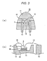
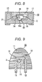
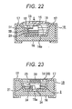
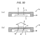
- a container for a semiconductor light-emitting device (such as a cup described later, hereinafter referred to as "container of semiconductor light-emitting device” as appropriate) is usually formed of a ceramic or a metal.
- a hydroxyl group usually exists on the surface of a ceramic and a metal.
- the polysilaxane cured product may have a functional group capable of forming a hydrogen bond with the hydroxyl group.
- the curable polysiloxane of the invention it is preferred for the curable polysiloxane composition of the invention that, among all the substituents bound to the silicon atom of the siloxane compounds contained in the curable polysiloxane composition, 80 mol% or more, preferably 95 mol% or more, further preferably 99 mol% or more of the substituent excluding the hydride group and the silanol group are an alkyl group.
- the alkyl group is preferably methyl group.
- the molar fraction of the substituent excluding the hydride group and the silanol group can be calculated as molar percentage by (molar ratio calculated from total area of peaks of alkyl groups bound to a silicon atom of siloxane compound)/(molar ratio calculated from total area of peaks of all substituents (excluding hydride group and hydroxyl group) bound to a silicon atom of siloxane compound) from the measured spectrum using liquid H-nuclear magnetic resonance spectrum, solid H-nuclear magnetic resonance spectrum, solid Si-nuclear magnetic resonance spectrum, or a complementary combination thereof.
- substituents R 1 to R 20 of the above general formulae (1), (2), and (3) it is preferable that 80 mol% or more, preferably 95 mol% or more, further preferably 99 mol% of the substituents excluding the hydride group and the hydroxyl group are an alkyl group, so that the content of the functional group capable of forming a hydrogen bond with that hydroxyl group preferably falls within the range.
- Examples of the functional group capable of forming a hydrogen bond with the hydroxyl group, which is possessed by the polysiloxane cured product of the invention include, for example, a silanol group, an alkoxy group, an amino group, an amino group, a methacryl group, an acryl group, a thiol group, an epoxy group, an ether group, a carbonyl group, a carboxyl group, a sulfonate group and the like.
- a silanol group and an alkoxy group are preferable from the viewpoint of heat resistance.
- one type of the functional group or two or more types of the functional groups may be used.
- the polysiloxane cured product of the invention has any functional group capable of forming a hydrogen bond with the hydroxyl group, as described above, can be checked by a spectroscopic technique such as solid Si-NMR, solid 1 H-NMR, infrared resonance spectrum (IR), Raman spectrum or the like.
- a spectroscopic technique such as solid Si-NMR, solid 1 H-NMR, infrared resonance spectrum (IR), Raman spectrum or the like.
- the polysiloxane cured product of the invention is excellent in heat resistance. That is, the polysiloxane cured product has a property that transmittance thereof with respect to light having a predetermined wavelength hardly varies even when left under a high temperature condition. More specifically, the maintenance rate of transmittance of the polysiloxane cured product of the invention with respect to the light having a wavelength of 400 nm before and after being kept for 500 hours at temperature of 200°C is usually 80% or more, preferably 90% or more and more preferably 95% or more, and usually 110% or less, preferably 105% or less and more preferably 100% less.
- the above ratio of variation can be measured in the same way as the method of measuring the UV transmittance, described earlier in [2-3-2], by means of measuring transmittance using an ultraviolet/visible spectrophotometer.
- the polysiloxane cured product of the invention is excellentr in light resistance. That is, the polysiloxane cured product of the invention has a property that transmittance thereof with respect to the light having a predetermined wavelength hardly varies even when irradiated with UV (ultraviolet light). More specifically, the maintenance rate of transmittance of the polysiloxane cured product of the invention with respect to the light having a wavelength of 400 nm before and after being irradiated with light whose central wavelength is 380 nm and radiant intensity is 0.4 kW/m 2 for 72 hours is usually 80% or more, preferably 90% or more and more preferably 95% or more, and usually 110% or less, preferably 105% or less and more preferably 100% or less.
- the above ratio of variation can be measured in the same way as the method of measuring the UV transmittance, described earlier in [2-3-2], by means of measuring transmittance using an ultraviolet/visible spectrophotometer.
- the polysiloxane cured product of the invention is usually produced using curing catalysts. Therefore, usually in the polysiloxane cured product of the invention, these catalysts are retained.
- the polysiloxane cured product of the invention comprises the above-mentioned curing catalysts in an amount of usually 0.001% by weight or more, preferably 0.01% by weight or more and more preferably 0.02% by weight or more, and usually 0.3% by weight or less, preferably 0.2% by weight or less and more preferably 0.1% by weight or less, in terms of a metal element.
- the above-mentioned content of the curing catalyst can be measured by ICP analysis.
- the integrated area of chromatogram, in TG-mass (pyrolytic MS chromatogram), of the gas generated by heating at the range of 40°C tat 210°C is small.
- TG-mass detects low-boiling components in the polysiloxane cured product by heating the polysiloxane cured product
- a large integrated area of chromatogram in the range of 40°C to 210°C indicates that low-boiling components such as water, solvent and three-membered to five-membered cyclic siloxanes are present in the component.
- the large amount of low-boiling components induces occurrence or bleed-out of air bubbles in the process of using the cured product, thereby lowering the adhesion to the container of semiconductor light-emitting device, and (ii) a heat generated during use induces occurrence or bleed-out of air bubbles.
- the polysiloxane cured product of the invention it is preferable for the polysiloxane cured product of the invention to comprise less low-boiling components.
- the polysiloxane cured product of the invention is preferably a member presenting elastomer properties.
- An optical member of a semiconductor light-emitting device or the like generally uses a plurality of members whose thermal expansion coefficients are different in many cases but the elastomer properties presented by the polysiloxane cured product of the invention can relieve stress caused by expansion and shrinkage of the members to be used in the optical member. Therefore, a semiconductor device that is resistant to a peeling, crack, and breaking of wire while in use and superior in reflow resistance and temperature cycling resistance can be provided.
- the measurement value of hardness (Shore A) by durometer type A, of the polysiloxane cured product is usually 5 or larger, preferably, 7 or larger, and still preferably 10 or larger, and usually 90 or smaller, preferably 80 or smaller, and still preferably 70 or smaller.
- the optical member of the invention can obtain such advantages as being more resistant to cracks and being superior in reflow resistance and temperature cycling resistance.
- the above measurement value of hardness can be measured according to a method described in JIS K6253. More specifically, the measurement can be made using an A-type rubber hardness tester manufactured by Kori Seiki MFG. Co., Ltd.
- the polysiloxane cured product of the invention may be used as an encapsulant singly.
- a phosphor that is liable to deteriorate by oxygen or moisture, or a semiconductor light-emitting device retention of the phosphor, encapsulating the semiconductor light-emitting element or extracting light is carried out with the polysiloxane cured product of the invention and further, an air-tight encapsulating with a highly air-tight material such as a glass plate or an epoxy resin may be carried out in the outer side of them, or vacuum encapsulating may be performed.
- the shape is not specially limited and it is enough that the encapsulated body, coating or coated surface by the polysiloxane cured product of the invention is substantially protected and blocked from outside by an air-tight material such as a metal, glass or highly air-light resin, so as to allow no passage of oxygen and moisture.
- an air-tight material such as a metal, glass or highly air-light resin
- the polysiloxane cured product of the invention may be used as an adhesive agent for a semiconductor light-emitting device because it is excellent in adhesion as described above. More specifically, for example, the polysiloxane cured product of the invention can be used in the cases of bonding a semiconductor element and a package, a semiconductor element and a sub mount, package constituents each other, a semiconductor light-emitting device and an external optical element, by means of application, printing or potting the polysiloxane cured product.
- the polysiloxane cured product of the invention is excellent particularly in light resistance and heat resistance, it provides a semiconductor light-emitting device with high reliability enough to stand a long-time use, when it is used as an adhesive for a high-power semiconductor light-emitting device that is exposed to high temperature or ultraviolet rays for a long time,
- the polysiloxane cured product of the invention can achieve sufficient adhesion just by itself, however, for the purpose of securing more sufficient adhesion, surface treatments for improving adhesion may be performed on the surface that will come directly in contact with the polysiloxane cured product.
- surface treatments for improving adhesion include, for example: a formation of an adhesion-improving layer using a primer or a silane coupling agent, a chemical surface treatment using a chemical agent such as an acid or an alkali, a physical surface treatment using plasma irradiation, ion irradiation or electron beam irradiation, a surface-roughening treatment by sandblasting, etching, microparticles coating or the like.
- the shape and the dimension of the polysiloxane cured product of the invention can be decided arbitrarily.
- the shape and the dimension of the polysiloxane cured product of the invention are decided according to the shape and the dimension of the container of the semiconductor light-emitting device.
- the polysiloxane cured product is formed on the surface of a certain substrate, it is often formed into a film shape, and the dimension thereof is set arbitrarily depending on its use.
- any shape can be used arbitrarily according to the site to be applied.
- one of the advantageous effects of the polysiloxane cured product of the invention is that it can be formed into a thick film when it is formed into a film shape.
- Optical members hitherto used are difficult in forming them into thick films, due to occurrence of cracks or the like caused by an internal stress or the like but, there are no such problems in the polysiloxane cured product of the invention and it can be formed into a thick film steadily.
- the upper limit thereof is usually 10 mm or smaller, preferably 5 mm or smaller and more preferably I mm or smaller.
- the "thickness of the film” indicates the thickness of the film at its thickest portion.
- the polysiloxane cured product of the invention can usually encapsulate a semiconductor light-emitting device for a longer period of time than conventional ones without generating cracks or peelings. More specifically, when a semiconductor light-emitting device is encapsulated with the polysiloxane cured product of the invention and the semiconductor light-emitting device is illuminated in a continuous manner at temperature of 85°C and relative humidity of 85% with usually 20 mA or more, preferably 350 mA or more of driving current, the luminance after usually 500 hours or longer, preferably 1000 hours or longer, more preferably 2000 hours or longer is not decreased as compared with that of just after switched on.
- the polysiloxane cured product may comprise other components, depending on its use.
- the polysiloxane cured product of the invention when used as a constituent member of a semiconductor light-emitting device or the like, it may comprise a phosphor, inorganic particles or the like. Explanation will be given on this point later, together with an explanation on the use.
- the other components may be used as only a single kind thereof or two or more kinds thereof may be used in any combination and in any ratio.
- the curable polysiloxane composition of the invention is obtained by mixing the above-mentioned hydrosilyl group-containing polysiloxane compound represented by the general formula (1), the above-mentioned polysiloxane compound represented by the general formula (2) and comprising two or more silanol groups in one molecule and the above-mentioned curing catalyst and, if necessary, the other additive(s).
- the mixing method is not particularly limited.
- the curable polysiloxane composition of the invention is obtained by mixing the above-mentioned hydrosilyl group-containing polysiloxane compound represented by the general formula (1), the above-mentioned polysiloxane compound represented by the general formula (2) and comprising two or more silanol groups in one molecule, the above-mentioned polysiloxane compound represented by the general formula (3) and comprising two or more alkenyl groups in one molecule, and the dehydrogenative condensation reaction catalyst and the addition condensation catalyst and, if necessary, the other additive(s).
- the mixing method is not particularly limited.
- the dehydrogenative condensation reaction of (1) and (2) and the addition polymerization reaction of (I) and (3) simultaneously proceed.
- the total amount of the silanol group in the composition is larger than the sum of the alkenyl group and the hydrosilyl group, the resulting cured product is a polysiloxane comprising a silanol group and excellent in adhesion.
- the dehydrogenative condensation reaction catalyst and the addition polymerization catalyst may be used separately but a catalyst possessing functions of a dehydrogenative condensation reaction catalyst and a addition polymerization catalyst, such as a platinum-based catalyst, may be used as a single kind.
- the method for producing the polysiloxane cured product of the invention is not limited as far as it has a process of curing the curable polysiloxane composition of the invention.
- the solvent may be removed by distillation in advance before drying.
- the polysiloxane cured product of the invention is usually cured under air at the temperature of 150°C within 6 hours. In carrying out the invention, the following will describe preferable curing conditions in detail.
- the curing treatment is performed in the range of usually 15°C or higher, preferably 50°C or higher, and more preferably 100°C or higher, and usually 300°C or lower, preferably 200°C or lower, and more preferably 170°C or lower in the case of performing under normal pressure. By maintaining a liquid phase under an elevated pressure, it is also possible to perform the treatment at a higher temperature.
- the curing time varies depending on the reaction temperature but is performed in the range of usually 0.1 hour or longer, preferably 0.5 hour or longer, and further preferably 0.8 hour or longer, and usually 100 hours or shorter, more preferably 20 hours or shorter, and further preferably 15 hours or shorter.
- the curable polysiloxane composition comprising no solvent (liquid semipolycondensate) can be obtained, which can be subjected to the polymerization as it is.
- a method of removing the solvent by distillation is arbitrary unless the advantages of the invention are remarkably impaired. However, it is suitable to avoid removing the solvent by distillation at a temperature equal to or higher than the decomposition start temperature of the curable polysiloxane composition.
- Specific range of the temperature condition at the removal of the solvent by distillation is usually 60°C or higher, preferably 80°C or higher, and more preferably 100°C or higher, and usually 450°C or lower, preferably 300°C or lower, and more preferably 200°C or lower.
- the temperature is lower then the lower limit of the range, there is a possibility that the removal of the solvent by distillation becomes insufficient and when the temperature is higher than the upper limit, there is a possibility that the curable polysiloxane composition is gelled.
- the pressure condition at the removal of the solvent by distillation is usually normal pressure. Further, if necessary, the pressure is reduced so that the boiling point of the reaction solution at the removal of the solvent by distillation does not reach the decomposition start temperature. Also, the lower limit of the pressure is around a pressure at which a main component of the curable polysiloxane composition is not removed by distillation.
- curing is preferably performed usually at a temperature equal to or lower than the heat-resistant temperature of the components of the semiconductor light-emitting device, preferably at a temperature of 200°C or lower.
- curing is possible at such a relatively low temperature as about 150°C or lower, so that curing is preferably performed at 150°C or lower in the case where stabilisation of the components of the semiconductor light-emitting device, particularly a semiconductor light-emitting element and a phosphor is intended.
- post-treatments may be performed on the resultant polysiloxane cured product, if necessary.
- the post-treatment include a surface treatment for improving the adhesion to the mold parts, preparation of antireflection film, preparation of a fine uneven surface for improving the efficiency of extracting light, and the like,
- the polysiloxane cured product of the invention is not particularly limited in its use and can be suitable used for various optical members owing to its excellency in various properties such as light transmittance (transparency), light resistance, heat resistance, hydrothermal resistance, UV resistance, and little-foaming property.
- Specific examples of the use of the optical members comprising the polysiloxane cured product of the invention include semiconductor light-emitting devices, optical guide plates, members for aerospace industry, and the like.
- the optical member comprising the polysiloxane cured product of the invention may be used with appropriately determining its shape, degree of transparency, and the like, depending on the use of the optical member, or the other compound such as a phosphor or an inorganic particle may be used in combination.
- these other compounds may be mixed into the curable polysiloxane composition and the resultant mixture may be used, for example.
- the optical member of the invention when used as a member (encapsulant) for encapsulating a semiconductor light-emitting element or the like of a semiconductor light-emitting device, the optical member can be more suitably used for specific use by using a phosphor particle and/or an inorganic particle in combination. In the following, such combined uses of a phosphor particle and an inorganic particle will be described.
- the polysiloxane cured product of the invention can be used as a member for wavelengths conversion by dispersing a phosphor in the polysiloxane cured product of the invention, which is molded inside a cup of a semiconductor light-emitting device as described below or applied as a thin film on an appropriate transparent support.
- a phosphor may be used singly or two or more kinds thereof may be used in any combination and in any ratio.
- composition of the phosphor there is no special limitation on the composition of the phosphor.
- a host crystal such as a metal oxide represented by Y 2 O 3 , Zn 2 SiO 4 or the like, a phosphate represented by Ca 5 (PO 4 ) 3 Cl or the like, and a sulfide represented by ZnS, SrS, CaS or the like is combined with an ion of a rare earth metal such as Ce, Pr, Nd, Pm, Sm, Eu, Tb, Dy, Ho, Er, Tm or Yb, or an ion of a metal such as Ag, Cu, Au, Al, Mn or Sb as an activator or coactivator.
- the host crystal include, for example, sulfides such as (Zn,Cd)S, SrGa 2 S 4 , SrS and ZnS; oxysulfides such as Y 2 O 2 S; aluminate such as (Y,Gd) 3 Al 5 O 12 , YAlO 3 , BaMgAl 10 O 17 , (Ba,Sr)(Mg,Mn)Al 10 O 17 , (Ba,Sr,Ca)(Mg,Zn,Mn)Al 10 O 17 , BaAl 12 O 19 , CeMgAl 11 O 19 , (Ba,Sr,Mg)O ⁇ Al 2 O 3 , BaAl 2 SiO 8 , SrAl 2 O 4 , Sr 4 Al 14 O 25 and Y 3 Al 5 O 12 ; silicate such as Y 2 SiO 5 and Zn 2 SiO 4 ; oxides such as SnO 2 and Y 2 O 3 ; borate
- red phosphor An example of the specific wavelength range of fluorescence emitted by a phosphor which emits red fluorescence (hereinafter referred to as "red phosphor" when appropriate) is preferably such that the peak wavelength thereof is usually 570 nm or longer, preferably 580 nm or longer, and usually 700 nm or shorter, preferably 680 nm or shorter.
- red phosphor examples include, for example, europium-activated alkaline earth silicon nitride phosphors represented by (Mg,Ca,Sr,Ba) 2 Si 5 N 8 :Eu, which are constituted by fractured particles having red fractured surfaces and emit light in the red region, europium-activated rare earth oxychalcogenide phosphors represented by (Y,La,Gd,Lu) 2 O 2 S:Eu, which are constituted by growing particles having nearly spherical shapes typical of regular crystal growth and emit light in the red region, and the like.
- phosphors which are described in JP-A-2004-300247 , comprising an oxynitride and/or an oxysulfide comprising at least one element selected from the group consisting of Ti, Zr, Hf, Nb, Ta, W and Mo, and also comprising an oxynitride having an ⁇ -sialon structure in which all or part of Al element is replaced by Ga element.
- phosphors comprising oxynitride and/or oxysulfide.
- red phosphor other than the above are: Eu-activated oxysulfide phosphors such as (LaY) 2 O 2 S:Eu; Eu-activated oxide phosphors such as Y(V,P)O 4 ;Eu and Y 2 O 3 :Eu; Eu,Mn-activated silicate phosphors such as (Ba,Sr,Ca,Mg) 2 SiO 4 :Eu,Mn and (Ba,M g ) 2 SiO 4 :Eu,Mn; Eu-activated sulfide phosphors such as (Ca,Sr)S:Eu; Eu-activated aluminate phosphors such as YAlO 3 :Eu; Eu-activated silicate phosphors such as LiY 9 (SiO 4 ) 6 O 2 :Eu, Ca 2 Y 8 (SiO 4 ) 6 O 2 :Eu, (Sr,Ba,Ca) 3 SiO
- red organic phosphors comprising rare earth element ion complexes comprising anions such as ⁇ -diketonates, ⁇ -diketones, aromatic carboxylic acids or Broensted acids as ligands, perylene pigments (for example, dibenzo ⁇ [f,f]-4,4',7,7'-tetraphenyl ⁇ diindeno[1,2,3-cd:1',2',3'-1m]perylene), anthraquinone pigments, lake pigments, azo pigments, quinacridone pigments, anthracene pigments, isoindoline pigments, isoindolinone pigments, phthalocyanine pigments, triphenylmethane-based basic dyes, indanthrone pigments, indophenol pigments, cyanine pigments and dioxazine pigments.
- perylene pigments for example, dibenzo ⁇ [f,f]-4,4',7,7'-t
- red phosphors those whose peak wavelength is 580 nm or longer, preferably 590 nm or longer, and 620 nm or shorter, preferable 610 nm or shorter can be suitably used as an orange phosphor.
- orange phosphors include: (Sr,Ba) 3 SiO 5 :Eu, (Sr,Mg) 3 (PO 4 ) 2 :Sn 2+ , SrCaAlSiN 3 :Eu, Eu-activated oxynitride phosphors such as Eu-activated ⁇ -sialon, and the like.
- Green phosphor An example of the specific wavelength range of fluorescence emitted by a phosphor which emits green fluorescence (hereinafter referred to as "green phosphor" when appropriate) is preferably such that the peak wavelength thereof is usually 490 nm or longer, preferably 500 nm or longer, and usually 570 nm or shorter, preferably 550 nm or shorter.
- Examples of such a green phosphors include, for example, europium-activated alkaline earth silicon oxynitride phosphors represented by (Mg,Ca,Sr,Ba)Si 2 O 2 N 2 :Eu, which are constituted by fractured particles having fractured surfaces and emit light in the green region, europium-activated alkaline earth silicate phosphors represented by (Ba,Ca,Sr,Mg) 2 SiO 4 :Eu, which are constituted by fractured particles having fractured surfaces and emit light in the green region, and the like.
- Eu-activated aluminate phosphors such as Sr 4 Al 14 O 25 ;Eu and (Ba,Sr,Ca)Al 2 O 4 :Eu
- Eu-activated silicate phosphors such as (Sr,Ba)Al 2 Si 2 O 8 :Eu, (Ba,Mg) 2 SiO 4 :Eu, (Ba,SrCa,Mg) 2 SiO 4 :Eu and (Ba,Sr,Ca) 2 (Mg,Zn)Si 2 O 7 :Eu
- Ce,Tb-activated silicate phosphors such as Y 2 SiO 5: Ce,Tb
- Eu-activated borophosphate phosphors such as Sr 2 P 2 O 7 -Sr 2 B 2 O 5 :Eu
- Eu-activated halosilicate phosphors such as Sr 2 Si 3 O 8 -2SrCl 2 :Eu
- green phosphor Also applicable as the green phosphor are: fluorescent dyes such as pyridinephthalimide condensation derivatives, benzoxadinone-based one, quinazoline-based one, coumarine-based one, quinophthalone-based one and nalthalimide-based one; and organic phosphors such as terbium complexes having hexyl salicylate as its ligand.
- fluorescent dyes such as pyridinephthalimide condensation derivatives, benzoxadinone-based one, quinazoline-based one, coumarine-based one, quinophthalone-based one and nalthalimide-based one
- organic phosphors such as terbium complexes having hexyl salicylate as its ligand.
- An example of the specific wavelength range of fluorescence emitted by a phosphor which emits blue fluorescence is such that the peak wavelength thereof is usually 420 nm or longer, preferably 440 nm or longer, and usually 480 nm or shorter, preferably 470 nm or shorter.
- Examples of such a blue phosphor include europium-activated barium magnesium aluminate phosphors represented by BaMgAl 10 O 17 :Eu, which are constituted by growing particles having nearly hexagonal shapes typical of regular crystal growth and emit light in the blue region, europium-activated calcium halphosphate phosphors represented by (Ca,Sr,Ba) 5 (PO 4 ) 3 Cl:Eu, which are constituted by growing particles having nearly spherical shapes typical of regular crystal growth and emit light in the blue region, europium-activated alkaline earth chloroborate phosphors represented by (Ca,Sr,Ba) 2 B 5 O 9 Cl:Eu, which are constituted by growing particles having nearly cubic shapes typical of regular crystal growth and emit light in the blue region, and europium-activated alkaline earth aluminate phosphors represented by (Sr,Ca,Ba)Al 2 O 4 :Eu or (SrCa,Ba) 4 Al 14 O
- blue phosphor other than the above Sn-activated phosphate phosphors such as Sr 2 P 2 O 7 :Sn; Eu-activated aluminate phosphors such as Sr 4 Al 14 O 25 :Eu, BaMgAl 10 O 17 :Eu and BaAl 8 O 13 :Eu; Ce-activated thiogallate phosphors such as SrGa 2 S 4 :Ce and CaGa 2 S 4 :Ce; Eu-activated aluminate phosphors such as (Ba,Sr,Ca)MgAl 10 O 17 :Eu and BaMgAl 10 O 17 :Eu,Tb,Sm; Eu,Mn-activated aluminate phosphors such as (Ba,Sr,Ca)MgAl 10 O 17 :Eu,Mn; Eu-activated halophosphate phosphors such as (Sr,Ca,Ba,
- blue phosphor are, for example: fluorescent dyes such as naphthalimide-based one, benzoxazole-based one, styryl-based one, coumarine-based one, pyrazoline-based one and triazole-based one; organic phosphors such as thulium complexes; and the like.
- yellow phosphor An example of the specific wavelength range of fluorescence emitted by a phosphor which emits yellow fluorescence (hereinafter referred to as "yellow phosphor" when appropriate) is usually 530 nm or longer, preferably 540 nm or longer, more preferably 550 nm or longer, and usually 620 nm or shorter, preferably 600 nm or shorter, more preferably 580 nm or shorter, If the emission peak wavelength of the yellow phosphor is too short, there is a possibility that yellow components may be decreased and the semiconductor light-emitting device may be inferior in color rendering. If it is too long, there is a possibility that the luminance of the semiconductor light-emitting device may be lowered.
- Examples of the yellow phosphor include, for example, various phosphors such as oxide, nitride, oxynitride, sulfide and oxysulfide phosphors. Particularly, examples include: garnet phosphors represented by RE 3 M 5 O 12 :Ce (where RE represents at least one element selected from Y, Tb, Gd, Lu and Sm, and M represents at least one element selected from Al, Ga and Sc), M 2 3 M 3 2 M 4 3 O 12 :Ce (where M 2 is a divalent metal element, M 3 is a trivalent metal element and M 4 is a tetravalent metal element) and the like, and having garnet structures; orthosilicate phosphors represented by AE 2 M 5 O 4 :Eu (where AE represents at least one element selected from Ba, Sr, Ca, Mg and Zn, and M 5 represents at least one element selected from Si and Ge) and the like; oxynitride phosphors in which a part of oxygen
- Eu-activated phosphors such as sulfide phosphors such as CaGa 2 S 4 :Eu, (Ca,Sr)Ga 2 S 4 :Eu and (Ca,Sr)(Ga,Al)S 4 :Eu; and oxynitride phosphors having SiAlON structures such as Cax(Si,Al) 12 (O,N) 16 :Eu.
- the polysiloxane cured product of the invention may comprise phosphors other than those cited above.
- the polysiloxane cured product or the invention may be a fluorescent glass in which an ionic phosphor material or an organic/inorganic phosphor component is dissolved or dispersed uniformly and transparently.
- the median particle diameter (D 50 ) thereof is usually 0.1 ⁇ m or larger, preferably 2 ⁇ m or larger, more preferably 5 ⁇ m or larger, and usually 100 ⁇ m or smaller preferably 50 ⁇ m or smaller, more preferably 20 ⁇ m or smaller.
- the median particle diameter (D 50 ) of the phosphors is within the above range, the light emitted from the semiconductor light-emitting element can be scattered sufficiently, in the semiconductor light-emitting device to be described later.
- the light emitted from the semiconductor light-emitting element is absorbed in the phosphor particles sufficiently, and therefore, not only the wavelength conversion is performed highly efficiently but also the light emitted from the phosphors is radiated in all directions.
- a white light can be obtained by mixing primary lights from the several kinds of phosphors and also a uniform whiteness can be obtained, so that a uniform white light and illumination intensity can be obtained in the synthesized light emitted from the semiconductor light-emitting device.
- the median particle diameter (D 50 ) of the phosphors is larger than the above range, the phosphors can not fill the space of the light-emitting part sufficiently, and therefore, there is a possibility that the light emitted from the semiconductor light-emitting element may not be absorbed in the phosphors sufficiently, in the semiconductor light-emitting device to be described later.
- the median particle diameter (D 50 ) of the phosphors is smaller than the above range, emission efficiency of the phosphors will be reduced, and therefore, there is a possibility that illumination intensity of the semiconductor light-emitting device may be reduced.
- the particle size distribution (QD) of the phosphor particles is smaller for the purpose of equalizing the dispersion state of the particles in the polysiloxane cured product.
- the smaller the particle size distribution is the lower the classification efficiency will be and therefore the higher the cost will be. For that reason, it is usually 0.03 or larger, preferably 0.05 or larger, more preferably 0.07 or larger, and usually 0.4 or smaller, preferably 0.3 or smaller, more preferably 0.2 or smaller.
- the median particle diameter (D 50 ) and particle size distribution (QD) can be obtained from a weight-standard particle size distribution curve.
- the weight-standard particle size distribution curve is obtained from the measurement of particle size distribution by laser diffraction/scattering method, and concretely, the measurement can be performed as follows.
- the shape of the phosphor particles is not particularly limited as far as the formation of the polysiloxane cured product is not affected.
- it is not limited as far as the fluidity or the like of the phosphor part formation liquid (namely, mixed liquid of the phosphor and the polysiloxane cured product) is not affected.
- a surface treatment may be performed to the phosphor used in the invention, for the purpose of enhancing the water resistance or preventing unnecessary aggregation of the phosphor in the polysiloxane cured product.
- a surface treatment include a surface treatment using an organic material, an inorganic material, a glass material, or the like as described in JP-A-2002-223008 , a coating treatment with a metal phosphate as described in JP-A-2000-96045 and the like, a coating treatment with a metal oxide, known surface treatments such as silica coating, and the like.
- the following surface treatment (i) to (iii) is performed.
- surface treatment examples include, as silica coating, a method in which SiO 2 is deposited by neutralizing a liquid glass, a method of surface treatment with a hydrolyzed alkoxysilane (for example, JP-A-3-231987 ) and the like.
- a hydrolyzed alkoxysilane for example, JP-A-3-231987
- the method of surface treatment with a hydrolyzed alkoxysilane is preferable from the standpoint of enhancing the dispersibility.
- the method of adding phosphor particles is not particularly limited. If phosphor particles are in a good dispersion state, it is sufficient only to post-mix phosphor particles into the above-mentioned curable polysiloxane composition. That is, it is sufficient to prepare a phosphor part formation liquid by mixing the curable polysiloxane composition of the invention and the phosphor, and to form a polysiloxane composition by using this phosphor part formation liquid.
- Some kinds of phosphors are hydrolyzable. However, in the polysiloxane cured product of the invention, almost no liberated water exists in a liquid state (curable polysiloxane composition) before coating, and therefore such phosphors can also be used without being hydrolyzed.
- phosphor particles or inorganic particles are dispersed in the polysiloxane cured product of the invention, it is possible to modify the surface of the particles with organic ligands in order to improve dispersibility.
- An addition type silicone resin which has previously been used as a semiconductor light-emitting device member, was liable to undergo cursing inhibition by these organic ligands and could not be mixed/cured with particles which had been subjected to such a surface treatment. This is because platinum-based catalyst used in the addition reaction type silicone resin interacts strongly with the organic ligands and loses capability of hydrosilylation, resulting in poor curing.
- the polysiloxane cured product of the invention is related to a condensing-type curing mechanism, which is less liable to undergo curing inhibition by these poisoning substances. Therefore, the polysiloxane cured product of the invention can be used more freely in combination with phosphor particles or inorganic particles, whose surfaces are modified with organic ligands, and further, with phosphor components such as complex phosphors. Thus, the polysiloxane cured product possesses an excellent property as a phosphor binder and a transparent material for introducing nano particles with high refractive index.
- the content of the phosphor in the polysiloxane cured product of the invention can be selected arbitrary insofar as the advantage of the invention is not significantly impaired. Actually, it can be selected freely depending on its form of applications.
- a semiconductor light-emitting device emitting white light which is used for white LED, white-light illuminating device or the like
- the total content of the phosphor is usually 0.1% by weight or more, preferably 1 % by weight or more, more preferably 5% by weight or more, and usually 35% by weight or less, preferably 30% by weight or less, more preferably 28% by weight or less.
- the total content is usually 5% by weight or more, preferably 7% by weight or more, more preferably 10% by weight or more, and usually 90% by weight or less, preferably 80% by weight or less, more preferably 70% by weight or less.
- the concentration of the phosphor tends to be as low as close to the lower limit of the above-mentioned range.
- the concentration of the phosphor is high. Therefore, in such a case, the concentration of the phosphor tends to be as high as close to the upper limit of the above-mentioned range.
- the content of the phosphor is more than this range, coating performance may be lowered, or low efficiency of phosphor utilization due to an optical interference, and therefore, there is a possibility that luminance of the semiconductor light-emitting device may be reduces. If the content of the phosphor is less than the range, there is a possibility that the wavelength conversion by the phosphor will be insufficient and therefore the intended emission color may not be obtained.
- the concrete content of the phosphor is not limited thereto and varies widely depending on the intended color, emission efficiency of the phosphors, color mixing method, specific gravity of the phosphors, film thickness of coating, shape of the semiconductor light-emitting device or the like.
- the curable polysiloxane composition of the invention has advantages such as low viscosity, good compatibility with phosphors or inorganic particles and good coating properties that can be maintained even when high concentration of phosphors or inorganic particles are dispersed therein, in comparison with the conventional material for optical members such as epoxy resins and silicone resins.
- the composition can be of high viscosity as needed by such a method of adjusting the degree of polymerization, and adding thixotropic agent such as aerosil.
- the composition is very flexible in adjustment of viscosity according to the intended content of phosphors. Therefore, it is possible to provide a coating liquid that can correspond flexibly to not only the kinds or shapes of coated objects but also various coating methods such as potting, spin coating and printing.
- the content of the phosphor in the polysiloxane cured product can be determined by the following procedure, if the composition of the phosphor can be identified.
- a phosphor-containing sample is prebaked after being pulverized so as to remove carbon components, followed by removing silicon components as hydrofluorosilicic acid by hydrofluoric acid treatment.
- the metal elements which are the main components, are converted into an aqueous solution and the quantity of the main component metal element is determined by known elemental analyses such as ICP, flame analysis or fluorescent X-ray analysis. Then, the content of the phosphor can be determined by calculation.
- the content of phosphor can be determined by a simplified method in which the number of the particles per unit area is obtained by image analysis of the cross section of the coating and then is converted into the content of phosphor.
- the phosphor content in the phosphor part formation liquid can be set so that the phosphor content in the polysiloxane cured product falls within the above range.
- the phosphor content in the phosphor part formation liquid will be equal to the phosphor, content in the polysiloxane cured product.
- the phosphor content in the phosphor part formation liquid other than the solvent or the like may be set so as to be the same as the phosphor content in the polysiloxane cured product.
- inorganic particles may be further contained for the purpose of improving the optical properties and workability, or obtaining any of effects ⁇ 1> to ⁇ 5> shown below.
- the inorganic particle When a fractured silica or spherical silica whose particle diameter is about several ⁇ m is used as the inorganic particle, it functions mainly as the aggregate for the polysiloxane cured product and increase in thixotropy is just a little, so that the effects of the above ⁇ 2> and ⁇ 4> are noticeable. Also, when inorganic particles having a diameter of about 1 ⁇ m, whose refractive index is different from that of the polysiloxane cured product, are used, the effect of the above ⁇ 1> is noticeable because the light scattering at the interface between the polysiloxane cured product and the inorganic particles increases.
- the kind of inorganic particles to be mixed may be selected according to the purposes. Only one kind thereof may be selected or a plurality kinds thereof may be combined. Also, in order to improve the dispersibility, a surface treatment may be applied with a surface treatment agent such as a silane coupling agent.
- Exemplified kinds of inorganic particles to be used include: inorganic oxide particles such as silica, barium titanate, titanium oxide, zirconium oxide, niobium oxide, aluminum oxide, cerium oxide and yttrium oxide; and diamond particles.
- inorganic oxide particles such as silica, barium titanate, titanium oxide, zirconium oxide, niobium oxide, aluminum oxide, cerium oxide and yttrium oxide
- diamond particles are examples of inorganic particles to be used.
- other materials can be also selected depending on the purposes and thus the inorganic particles are not limited thereto.
- Inorganic particles may be in any form, depending on the purposes, such as a powder and a slurry. However, when the transparency must be maintained, it is preferable to equalize the refractive indexes of the inorganic particles and the polysiloxane cured product of the invention or to add the particles as aqueous or solvent-based transparent sol to the curable polysiloxane composition.
- the median particle diameter of these inorganic particles There is no special limitation on the median particle diameter of these inorganic particles (primary particles). Usually, it is about 1/10 or less that of phosphor particles. More specifically, the following median particle diameter is adopted depending on the purpose. For example, when the inorganic particle is used as a light scattering agent, the median particle diameter thereof preferably falls within 0.1 ⁇ m to 10 ⁇ m. For example, when the inorganic particle is used as an aggregate, the median particle diameter thereof preferably falls within 1 nm to 10 ⁇ m. For example, when the inorganic particle is used as a thickener (thixotropic agent), the median particle diameter thereof preferably falls within 10 nm to 100 nm. For example, when the inorganic particle is used as a refractive index adjusting agent, the median particle diameter thereof preferably falls within 1 nm to 10 nm.
- the content of the inorganic particle in the polysiloxane cured product of the invention can be selected arbitrary insofar as the advantage of the invention is not significantly impaired. Actually, it can be selected freely depending on its form of applications.
- the content thereof preferably falls within 0.01 to 10% by weight
- the content thereof preferably falls within 1 to 50% by weight.
- the inorganic particle is used as a thickener (thixotropic agent)
- the content thereof preferably falls within 0.1 to 20% by weight.
- the inorganic particle is used as a refractive index adjusting agent
- the content thereof preferably falls within 10 to 80% by weight.
- the amount of inorganic particle is too small, there is a possibility that the desired advantageous effects may be unobtainable.
- the amount is too large, there is a possibility that various properties such as adhesion, transparency and hardness of the cured product may be affected adversely.
- the curable polysiloxane composition of the invention has advantages such as low viscosity, high compatibility with phosphors or inorganic particles and good coating properties that can be maintained even when high concentration of inorganic particles are dispersed therein, in comparison with the conventional materials for optical members, such as epoxy resins and silicone resins. Moreover, it can be of high viscosity as needed by such a method of adjusting the degree of polymerization and adding a thixotropic agent such as aerosil. Namely, the composition is very flexible in adjustment of viscosity according to the intended content of inorganic particles. Therefore, the composition can provide a coating liquid that can correspond very flexibly to not only the kinds or shapes of coated objects but also the various coating methods such as potting, spin coating and printing.
- the content of the inorganic particles in the polysiloxane cured product can be measured in the same manner as in the case of the above-described content of phosphor.
- the inorganic particle content in the curable polysiloxane composition can be set so that the inorganic particle content in the polysiloxane cured product falls within the above range.
- the inorganic particle content in the curable polysiloxane composition will be equal to the inorganic particle content in the polysiloxane cured product.
- the inorganic particle content in the curable polysiloxane composition other than the solvent or the like may be set so as to be the same as the inorganic particle content in the polysiloxane cured product.
- a conductive filler may be also contained, for example when the optical member comprising at least the polysiloxane cured product of the invention is used for a semiconductor light-emitting device, for the purpose of imparting electric conductivity and forming an electric circuit at a lower temperature than the temperature used at soldering using a technique such as printing or potting.
- Examples of conductive filler to be used include precious metal powders such as silver powder, gold powder, platinum powder and palladium powder, base/precious metal powders such as copper powder, nickel powder, aluminum powders, brass powder and stainless steel powder, base/precious metal powders plated or alloyed with a precious metal such as silver, organic resin powders or silica powders coated with a precious metal or a base metal, and carbon-based fillers such as carbon black or graphite powder.
- precious metal powders such as silver powder, gold powder, platinum powder and palladium powder
- base/precious metal powders such as copper powder, nickel powder, aluminum powders, brass powder and stainless steel powder
- base/precious metal powders plated or alloyed with a precious metal such as silver, organic resin powders or silica powders coated with a precious metal or a base metal
- carbon-based fillers such as carbon black or graphite powder.
- the conductive filler may be used either as a single kind, or two or more kinds thereof
- the conductive filler may be supplied in any form such as powder or scurry, depending on the purpose.
- it is preferably added to the curable polysiloxane composition as aqueous or solvent-based transparent sol with no aggregation or as nano particle powder with its surface modified to allow easy redispersion.
- these metal powders include flake (scale), sphere, grain, dendrite, and three-dimensional aggregation of spherical primary particles.
- the use of silver powder as main component is preferable from the standpoint of conductivity, cost and reliability. In terms of conductivity, combined use of silver powder and a small amount of carbon black and/or graphite powder is more preferable.
- the use of silver powder in the form of flake or sphere is preferable, and the combined use of flake and sphere silver powders is most preferable.
- an inorganic filler such as silica, talc, mica, barium sulfate or indium oxide may be added in a small amount, if needed.
- Preferable proportion (mass ratio) of silver powder and carbon black and/or graphite fine powder is as follows. On the supposition that the total amount of silver powder and carbon black and/or graphite fine, powder is 100 mass ratio, the upper limit of silver powder is preferably 99.5 mass ratio or less, more preferably 99 mass ratio or less, and the lower limit thereof is 85 mass ratio or more, preferably 90 mass ratio or more.
- the median particle diameter of the conductive filler is 0.1 ⁇ m or larger, preferably 0.5 ⁇ m or larger, and more preferably 1 ⁇ m or larger, and usually 50 ⁇ m or smaller, preferably 20 ⁇ m or smaller, and more preferably 10 ⁇ m or smaller.
- it is usually 3 nm or larger, preferably 10 nm or larger, and usually 150 mn or smaller, preferably 100 nm or smaller.
- the content of the conductive filler is usually 50% by weight or more, preferably 75% by weight or more, and more preferably 80% by weight or more, assuming that the total amount of the conductive filler and the binder resin is 100% by weight. From the viewpoint of adhesion and ink viscosity, it is usually 95% by weight or less, preferably 93% by weight or less, and more preferably 90% by weight or less.
- the amount of the conductive filler is too small, there is a possibility that the desired advantageous effects may be unobtainable.
- the amount is too large, there is a possibility that various properties such as adhesion, transparency and hardness of the cured product may be affected adversely.
- a heat conductive filler may be also contained, for example, when the optical member comprising at least the polysiloxane cured product of the invention is used in the semiconductor light-emitting device, for the purpose of imparting heat conductivity and providing a die-bonding layer using a technology such as printing or potting.
- the heat conductive filler to be used examples include precious metal powders such as silver powder, gold powder, platinum powder and palladium powder, base/precious metal powders such as copper powder, nickel powder, aluminum powder, brass powder and stainless steel powder, base/precious metal powders plated or alloyed with a precious metal such as silver, carbon-based fillers such as carbon black or graphite powder, ceramics powders such as SiC and SiN, diamond powder, and the like.
- carbon-based fillers such as carbon black or graphite powder
- ceramics powders such as SiC and SiN, diamond powder, and the like.
- the heat conductive filler may be used either as a single kind, or two or more kinds thereof may be used in any combination and in any ratio.
- the used amount and particle diameter of the heat conductive filler are preferably the same as those of the above-mentioned conductive filler.
- the curable polysiloxane composition of the invention has advantages such as low viscosity, high compatibility with phosphors or inorganic particles and sufficient coating properties that can be maintained even when high concentration of inorganic particles are dispersed therein, in comparison with the conventional materials for optical members, such as epoxy resins and silicone resins. Moreover, it can be of high viscosity as needed by such a method of adjusting the degree of polymerization and adding a thixotropic agent such as aerosil. Namely, the composition is very flexible in adjustment of viscosity according to the intended content of inorganic particles. Therefore, the composition can provide a coating liquid that can correspond very flexibly to not only the kinds or shapes of coated objects but also the various coating methods such as potting, spin coating and printing.
- the content of the inorganic particles in the curable polysiloxane composition can be measured in the same manner as in the case of the above-described content of phosphor.
- the curable polysiloxane composition of the invention may be used as an encapsulant singly.
- retention of the phosphor, encapsulating the semiconductor element or extracting light is carried out with the member of the invention and further, an air-tight encapsulating with a highly air-tight material such as a glass plate or an epoxy resin may be carried out in the outer side of them, or vacuum encapsulating may be performed.
- the shape of the semiconductor light-emitting device is not specially limited and it is enough that the encapsulated body, coating or coated surface by the curable polysiloxane composition of the invention is substantially protected and blocked from outside by an air-tight material such as a metal, glass or highly air-tight resin, so as to allow no passage of oxygen and moisture.
- an air-tight material such as a metal, glass or highly air-tight resin
- the curable polysiloxane composition of the invention may be used as an adhesive for a semiconductor light-emitting device because it is excellent in adhesion as described above.
- the polysiloxane cured product of the invention can be used in the cases of bonding a semiconductor element and a package, a semiconductor element and a sub mount, package constituents each other, a semiconductor light-emitting device and an external optical element, by means of application, printing or potting the polysiloxane cured product.
- the polysiloxane cured product of the invention is excellent particularly in light resistance and heat resistance, it provides a semiconductor light-emitting device with high reliability enough to stand a long-time use, when the polysiloxane cured product is used as an adhesive for a high-power semiconductor light-emitting device that is exposed to high temperature or ultraviolet rays for a long time.
- the polysiloxane cured product of the invention can achieve sufficient adhesion just by itself.
- surface treatments for improving adhesion may be performed on the surface that will come directly in contact with the polysiloxane cured product.
- Examples of such surface treatment include, for example: a formation of an adhesion-improving layer using a primer or a silane coupling agent, a chemical surface treatment using a chemical agent such as an acid or an alkali, a physical surface treatment using plasma irradiation, ion irradiation or electron beam irradiation, a surface-roughening treatment by sandblasting, etching, fine particles coating and the like.
- the semiconductor light-emitting device comprising at least the optical member of the invention (hereinafter referred to as a "semiconductor light-emitting device of the invention" when appropriate) will be explained with reference to embodiments thereof.
- the semiconductor light-emitting device of the invention is abbreviated as a "light-emitting device” when appropriate.
- the optical member of the invention to be used for the semiconductor light-emitting device of the invention is referred to as a semiconductor light-emitting device member.
- a site at which the optical member of the invention is used will be described all at once after the description of all the embodiments. However, these embodiments are used only for convenience of description, and therefore, the examples of the semiconductor light-emitting device comprising at least the optical member of the invention are not limited to these embodiments.
- the semiconductor light-emitting devices of the invention using the semiconductor light-emitting device member of the invention includes the following application examples A) and B).
- the semiconductor light-emitting device member of the invention shows excellent light resistance and heat resistance, less frequent crack generation and peeling, as well as less decrease in luminance, as compared to conventional optical members for semiconductor light-emitting devices. Therefore, a member exhibiting high reliability over a long period of time can be provided, by the semiconductor light-emitting device member of the invention.
- the semiconductor light-emitting device member of the invention can demonstrate superior capabilities similar to those in the above-mentioned application example A).
- it makes possible to form a phosphor part that is highly durable and can extract light with high efficiency, by retaining a phosphor or phosphor components.
- the semiconductor light-emitting device member of the invention retains a transparent and highly refractive component in addition to the phosphor or phosphor components, the interface reflection can be reduced and thus it becomes possible to obtain higher efficiency of extracting light, by adjusting the refractive index of the semiconductor light-emitting device member of the invention to be close to that of the light-emitting element or the phosphor.
- FIG. 50(a) and Fig. 50(b) are explanatory drawings of the basic concept of each embodiment.
- Fig. 50(a) corresponds to the above application example A)
- Fig. 50(b) corresponds to the above application example B).
- the light emitting devices (semiconductor light-emitting devices) 1A, 1B of each embodiment comprises a light-emitting element 2 comprised of an LED chip and a semiconductor light-emitting device member 3A, 3B of the invention, disposed close to the light-emitting element 2.
- light emitting device 1A does not comprise any phosphor or phosphor component in semiconductor light-emitting device member 3A.
- semiconductor light-emitting device member 3A performs various functions such as encapsulating of light-emitting element 2, extracting light and retaining functional components.
- semiconductor light-emitting device member 3A comprising no phosphor or phosphor component will be called a "Transparent member" when appropriate.
- light emitting device 1B comprise a phosphor or phosphor component in semiconductor light-emitting device member 3B.
- semiconductor light-emitting device member 38 can perform a function of wavelength conversion, in addition to the functions that can be performed by semiconductor light-emitting device member 3A in Fig, 50(a) .
- semiconductor light-emitting device member 3B comprising a phosphor or phosphor component will be called a "phosphor part" when appropriate.
- the phosphor part may be shown by numerals 33 and 34 according to its shape or functions when appropriate.
- Light-emitting element 2 is comprised of an LED chip emitting blue light or ultraviolet light, but it may be an LED chip of other emission color.
- Transparent member 3A performs functions of a highly durable encapsulant for light-emitting element 2, light extracting film, various-functions adding film and the like. Transparent member 3A may be used alone, Otherwise, it can comprise any additives, excluding the phosphor and phosphor components, as far as the advantage of the invention is not significantly impaired.
- Phosphor part 3B can perform not only functions of a highly durable encapsulant for light-emitting element 2, light extracting film, various-functions adding film and the like, but also a function of wavelength conversion, that is, a function to emit light of the desired wavelength after the excitation by the light from light-emitting element 2.
- Phosphor part 3B has to comprise at least a phosphor material that emits light of the desired wavelength after being excited by the light from light-emitting element 2. Examples of such a phosphor material include various phosphors exemplified above.
- Emission colors of the light that can be emitted by phosphor part 3B include white of a fluorescent lamp and yellow of a light bulb, as well as three primary colors red (R), green (G) and blue (B).
- phosphor part 3B has a wavelength conversion function for emitting light of the desired wavelength that is different from that of the excitation light.
- light 4 emitted from light-emitting element 2 passes through transparent member 3A to be emitted out of light emitting device 1A. Therefor, in light emitting device 1A, light 4 emitted from light-emitting element 2 will be used unchanged in emission color of the light emitted from light-emitting element 2.
- light 4a a part of the light emitted from light-emitting element 2 passes through phosphor part 3B unchanged to be emitted out of light emitting device 1B
- light 4b another part of the light emitted from light-emitting element 2 is absorbed by phosphor part 3B, resulting in that phosphor part 3B is excited and light 5 having wavelengths specific to phosphor components contained in phosphor part 3B, such as phosphor particles, fluorescent ions and fluorescent dyes, is emitted out of light emitting device 1B.
- synthesized light 6 synthesized from light 4a which has passed through phosphor part 3B after being emitted from light-emitting element 2, and light 5, which is emitted from phosphor part 3B, will be emitted from light emitting device 1B as light with converted wavelength.
- the emission color of the whole light emitted from light emitting device 1B will be determined by the emission color of light-emitting element 2 and that of phosphor part 3B.
- light 4a, which passes through phosphor part 3B after being emitted from light-emitting element 2 is not always necessary.
- light-emitting element 2 is surface-mounted on an insulating substrate 16 on which printed wiring 17 is provided.
- a p-type semiconductor layer (not shown) and an n-type semiconductor layer (not shown) in light-emitting layer part 21 are each connected electrically to printed wirings 17 and 17 via conductive wires 15 and 15, respectively.
- Conductive wires 15 and 15 have a small cross sectional area so that the light emitted from light-emitting element 2 may not be interfered.
- light-emitting element 2 one that emits light of any wavelengths, from ultraviolet to infrared regions, may be used.
- a gallium nitride-based LED chip is assumed to be used.
- an n-type semiconductor layer (not shown) is formed on the lower side in Fig. 1 and a p-type semiconductor layer (not shown) is formed on the upper side in Fig. 1 .
- the upper side of Fig. 1 is assumed to be the front side in the following description because light output is extracted from the side of the p-type semiconductor layer.
- a frame-shaped frame 18 surrounding light-emitting element 2 is fixed on the insulating substrate 16.
- a encapsulating part 19 for encapsulating and protecting light-emitting element 2 is provided inside the frame 18.
- This encapsulating part 19 is formed of transparent member 3A, which is the semiconductor light-emitting device member of the invention, and the formation thereof can be performed by potting with the raw material of the above polysiloxane cured product.
- light emitting device 1A of the present embodiment comprises light-emitting element 2 and transparent member 3A, the light resistance and heat resistance of light emitting device 1A can be improved.
- crack generation and peeling are less likely to occur in encapsulating part 3A, the transparency in encapsulating part 3A can be increased.
- the color blurring and color unevenness can be reduced and also the efficiency of extracting light to the outside can be enhanced, in comparison with conventional devices.
- encapsulating part 3A can be allowed to have high transparent without causing blurring and turbidity.
- light emitting device 1A is superior in uniformity in color appearance with little color unevenness among the light emitting devices 1A, and also can enhance the efficiency of extracting light from light-emitting element 2 to the outside, as compared with conventional devices.
- the weather resistance of the light-emitting material can be enhanced and thus the lifetime of light emitting device I A can be prolonged in comparison with conventional devices.
- Light emitting device 1A of the present embodiment is constituted, as shown in Fig. 2 , in the same manner as the above embodiment A-1, except that the front side of light-emitting element 2 is covered with transparent member 3A and the encapsulating part 19, formed on the transparent members, is formed of a material different from that of transparent member 3A.
- Transparent member 3A on the surface of light-emitting element 2 is a transparent thin film, functioning as a light extracting film and encapsulating film.
- Transparent member 3A can be formed, for example, by coating the above raw material of the polysiloxane cured product, by a method of spin coating or the like, during the formation of a chip of light-emitting element 2. Meanwhile, the same components as in the embodiment A-1 are designated by the same reference numerals to omit redundant explanations.
- light emitting device 1A of the present embodiment also comprises light-emitting element 2 and transparent member 3(a), like the embodiment A-1, the light resistance and heat resistance of light emitting device 1A, can be improved. Moreover, since crack generation and peeling are also less likely to occur in encapsulating part 3A, the transparency in encapsulating part 3A can be increased. Further, advantages, like those of embodiment A-1, can be also obtained.
- Light emitting device 1B of the present embodiment comprises, as shown in Fig. 3 (a) , light-emitting element 2 comprised of an LED chip and a mold part 11 obtained by forming a light-transmissible and transparent material into a shell type shape. Mold part 11 covers light-emitting element 2.
- Light-emitting element 2 is electrically connected to lead terminals 12 and 13, formed of a conductive material. Lead terminals 12 and 13 are formed of a lead frame.
- Light-emitting element 2 is comprised of a gallium nitride-based LED chip.
- an n-type semiconductor layer (not shows) is formed on the lower side in Fig. 3 (a) and a p-type semiconductor layer (not shown) is formed on the upper side in Fig. 3(a) .
- the upper sides of Fig. 3 are assumed to be the front sides in the following description because light output is extracted from the side of the p-type semiconductor layer.
- the rear surface of light-emitting element 2 is joined to a mirror (cup part) 14, which is attached to the front end part of lead terminal 13 by die bonding.
- Light-emitting element 2 in which the above p-type semiconductor layer and n-type semiconductor layer are connected to conductive wires (for example, gold wires) 15 and 15 by bonding, respectively, is electrically connected to lead terminals 12 and 13 via conductive wires 15 and 15, Conductive wires 15 and 15 have a small cross sectional area so that the light emitted from light-emitting element 2 may not be interfered.
- conductive wires for example, gold wires
- Mirror 14 has a function to reflect light emitted from both lateral sides and the rear surface of light-emitting element 2 forward.
- the light emitted from the LED chip and light reflected by mirror 14 in the front direction are emitted forward via the front end part of mold part 11, which functions as a lens.
- the mold part 11 covers light-emitting element 2 along with mirror 14, conductive wires 15 and 15, and a part of lead terminals 12 and 13, so that the degradation of properties of liglit-emitting element 2, due to a reaction with moisture in the air or the like, is prevented.
- the rear ends of each lead terminals 12 and 13 project from the rear surface of mold part 11.
- light-emitting layer part 21 composed of a gallium nitride-based semiconductor, is formed on phosphor part 3B by means of a semiconductor process.
- a reflective layer 23 is formed on the rear surface of phosphor part 3B.
- Light emitted from light-emitting layer part 21 is emitted in all directions, but a part of that light, which is absorbed by phosphor part 3B, excites phosphor part 3B to emit light having wavelength specific to the above-mentioned phosphor components.
- This light, emitted from phosphors part 3B is reflected by reflective layer 3 to be emitted forward. Therefore, light, synthesized from the light emitted from light-emitting layer part 21. and light emitted from phosphor part 3B, is obtained in light emitting device 1B.
- light emitting device 1B of the present embodiment comprises light-emitting element 2 and phosphor part 3B which emits light of the desired wavelength after being excited by the light from light-emitting element 2.
- phosphor part 3B is superior in light-transmission, a part of the light emitted from light-emitting element 2 is emitted unchanged to the outside, and the phosphor components, which play the role of emission center, are excited by another part of the light emitted from light-emitting element 2 and emits light, which is specific to the phosphor components, to the outside,
- light emitting device 1B is superior in uniformity in color appearance with little color unevenness among light-emitting devices 1B, and also can enhance the efficiency of extracting light from light-emitting element 2 to the outside, as compared with conventional devices. Also, the weather resistance of the light-emitting material can be enhanced and thus the lifetime of light emitting device 1B can be prolonged in comparison with conventional devices.
- phosphor part 3B serves also as a substrate for forming light-emitting element 2, and therefore the phosphor in the phosphor part, which play the role of emission center, can efficiently be excited by a part of the light from light-emitting element 2, leading to the enhancement in luminance of the emitted light specific to the phosphor components.
- light-emitting element 2 is surface-mounted on an insulating substrate 16 on which printed wiring 17 is provided.
- light-emitting element 2 is constituted in the same manner as in embodiment B-1, in which light-emitting layer part 21, composed of a gallium nitride-based semiconductor, is formed on phosphor part 3B and reflective layer 23 is formed on the rear surface of phosphor part 3B.
- a p-type semiconductor layer (not shown) and an n-type semiconductor layer (not shown) in light-emitting layer part 21 are connected electrically to printed wirings 17 and 17 via conductive wires 15 and 15, respectively.
- a frame-shaped frame 18 surrounding light-emitting element 2 is fixed on the insulating substrate 16.
- An encapsulating part 19 for encapsulating and protecting light-emitting element 2 is provided inside frame 18.
- light emitting device 1B in the present embodiment also comprises light-emitting element 2 and phosphor part 3B, which emits light of the desired wavelength after being excited by the light from light-emitting element 2, similarly to Embodiment B-1, light, synthesized from the light from light-emitting element 2 and light from the phosphor, can be obtained. Also, like Embodiment B-1, it becomes possible to reduce the color blurring and color unevenness, enhance the efficiency of extracting light to the outside, and as well as prolong the lifetime, in comparison with conventional devices.
- Light emitting device 1B of the present embodiment has a basic structure that is about the same as that in Embodiment B-2.
- frame 18 (see Fig. 4 ) described in Embodiment B-2 is not used and, as shown in Fig. 5 , the shape of encapsulating part 19 is different, Meanwhile, the same components as in embodiment B-2 are designated by the same reference numerals to omit redundant explanations.
- Encapsulating part 19 in the present embodiment comprises encapsulating function part 19a in a truncated cone shape for encapsulating light-emitting element 2 and a lens function part 19b in a lens shape to function as a lens at the front end part of encapsulating part 19.
- light emitting device 1B of the present embodiment can reduce the number of components, compared with Embodiment B-2, allowing the miniaturization and weight reduction.
- lens function part 19b functioning as a lens at one part of encapsulating part 19 distribution of light that is superior in directivity can be obtained.
- Light emitting device 1B of the present embodiment has a basic structure that is about the same as that in Embodiment B-2. As shown in Fig. 6 , it is characterized in that a hollow 16a for accommodating light-emitting element 2 is provided on one surface (upper surface in Fig. 6 ) of insulating substrate 15, light-emitting element 2 is mounted at the bottom of hollow 16a, and encapsulating part 19 is provided inside hallow 16a.
- printed wirings 17 and 17, formed on insulating substrate 16 are extended to the bottom of hollow 16a, and connected electrically to light-emitting layer part 21, composed of a gallium nitride-based semiconductor, in light-emiting element 2 via conductive wires 15 and 15.
- the same components as in embodiment B-2 are designated by the same reference numerals to omit redundant explanations.
- encapsulating part 19 of light emitting device 1B of the present embodiment is formed by filling hollow 16a, formed on the upper surface of insulating substrate 16, and therefore encapsulating part 19 can be formed without using frame 18 (see Fig. 5 ) described in Embodiment B-2 or the molding die described in Embodiment B-3. This advantageously simplifies the encapsulating process of light-emitting element 2, compared with Embodiments B-2 and B-3.
- Light emitting device 1B of the present embodiment has a basic structure that is about the same as that in Embodiment B-4. As shown in Fig. 7 , it is characterized in that light-emitting element 2 is so-called flip-chip-mounted on insulating substrate 16. That is, light-emitting element 2 is provided with bumps 24 and 24, made of conductive material, on the respective surface side of the p-type semiconductor layer (not shown) and n-type semiconductor layer (not shown) in light-emitting layer part 21, and light-emitting layer part 21 is electrically connected to printed wiring 17 and 17 of insulating substrate 16, with its face down, via bumps 24 and 24.
- light-emitting layer part 21 is disposed on the side nearest to insulating substrate 16
- reflective layer 23 is disposed on the side farthest from insulating substrate 16
- phosphor part 3B is sandwiched by light-emitting layer part 21 and reflective layer 23.
- the same components as in embodiment B-4 are designated by the same reference numerals to omit redundant explanations.
- the light reflected by reflective layer 23 in the downward (back) direction in Fig. 7 is then reflected by the inner circumferential surface of hollow 16a to be emitted in the upward (front) direction in Fig. 7 .
- light emitting device 1B of the present embodiment does not required conductive wires 15 and 15 like those in Embodiment B-4 for connecting printed wirings 17 and 17 provided on insulating substrate 16 and light-emitting element 2, This enables improvement in mechanical strength and reliability, compared with Embodiment B-4.
- Light emitting device 1B of the present embodiment has a basic structure that is about the same as that in Embodiment B-5. However, as shown in Fig. 8 , it is different in that reflective layer 23, described in Embodiment B-5, is not provided. In other words, in light emitting device 1B of the present embodiment, the light emitted from light-emitting layer part 21 and light emitted from phosphor part 3B are emitted in the front directions directly after passing through encapsulating part 19. Meanwhile, the same components as in embodiment B-5 are designated by the same reference numerals to omit redundant explanations.
- light emitting device 1B of the present embodiment can reduce the number of components, compared with Embodiment B-5, which results in facilitating the manufacture thereof.
- Light emitting device 1B of the present embodiment has a basic structure that is about the same as that in Embodiment B-1, As shown in Fig. 9 , it is characterized in that mold part 11, covering light-emitting element 2, is provided and mold part 11 is formed integrally with the phosphor part, Meanwhile, the same components as in Embodiment B-1 are designated by the same reference numerals to omit redundant explanations.
- mold part 11 is formed by a method, for example, in which a product in progress without mold part 11 is immersed in a molding die storing a phosphor part formation liquid and the phosphor part formation liquid (polycondensation product) is cured. Since mold part 11 and the phosphor part are integrally formed in the present embodiment, it becomes possible to enhance encapsulating properties, transparency, light resistance and heat resistance of mold part 11 and to inhibit crack generation and peeling accompanying a long-term use, by means of using the semiconductor light-emitting device member of the invention as phosphor part, as described later.
- Light emitting device 1B of the present embodiment has a basic structure that is about the same as that in Embodiment B-1. As shown in Fig. 10 , it is characterized in that a cup-shaped phosphor part 3B whose rear surface is open is mounted on the outer surface of mold part 11. That is, in the present embodiment instead of providing phosphor part 3B in light-emitting element 2 like Embodiment B-1, phosphor part 3B in a shape along an outer circumference of mold part 11 is provided. Meanwhile, the same components as in Embodiment B-1 are designated by the same reference numerals to omit redundant explanations.
- Phosphor part 3B in the present embodiment may be formed as a thin film by the method of curing the phosphor part formation liquid (polycondensation product) as described in Embodiment B-7. Otherwise, it may be formed by mounting a member, in which a solid phosphor part is molded in a cup-shape in advance, on mold part 11.
- the amount of the material used for the phosphor part can be reduced, compared with the case of light emitting device 1B of Embodiment B-7, in which the whole mold part 11 is formed integrally with the phosphors part, as well as cost reduction is achieved.
- Light emitting device 1B of the present embodiment has a basic structure that is about the same as that in Embodiment B-2. As shown in Fig. 11 , it is characterized in that frame-shaped frame 18, surrounding light-emitting element 2 on one surface (upper surface in Fig. 11 ) of insulating substrate 16, is provided and encapsulating part 19 inside frame 18 is formed of a phosphor part same as that of phosphor part 3B described in Embodiment B-2. Meanwhile, the same components as in embodiment B-2 are designated by the same reference numerals to omit redundant explanations.
- encapsulating part 19 is formed of the phosphor part in the present embodiment, it becomes possible to enhance encapsulating properties, transparency, light resistance, heat resistance and the like of encapsulating part 19 and to inhibit crack generation and peeling accompanying a long-term use, by means of using the semiconductor light-emitting device member of the invention as phosphor part, as described later.
- Light emitting device 1B of the present embodiment has a basic structure that is about the same as that in Embodiment B-2. As shown in Fig. 12 , it is characterized in that a frame-shaped frame 18, surrounding light-emitting element 2 on one surface (upper surface in Fig. 12 ) of insulating substrate 16, is provided and encapsulating part 19 inside frame 18 is formed of a phosphors part same as that of phosphors part 3B described in Embodiment B-2. Meanwhile, the same components as in embodiment B-2 are designated by the same reference numerals to omit redundant explanations.
- encapsulating part 19 is formed of the phosphor part in the present embodiment, it becomes possible to enhance encapsulating properties, transparency, light resistance, heat resistance and the like of encapsulating part is and to inhibit crack generation and peeling accompanying a long-term use, by means of using the semiconductor light-emitting device member of the invention as phosphor part, as described later, Furthermore, in the present embodiment, phosphor part 3B is formed on the rear surface of light-emitting layer part 21 in light-emitting element 2, and encapsulating part 19 covering light-emitting element 2 is formed of a phosphor part. This results in that the phosphor parts are present in all directions from light-emitting layer part 21 of light-emitting element 2. This structure leads to the advantageous effect that excitation and emission of the phosphor parts can be performed more efficiently than Embodiment B-9.
- Light emitting device 1B of the present embodiment has a basic structure that is about the same as that in Embodiment B-2. As shown in Fig. 13 , it is characterized in that phosphors part 33 formed in advance in a lens shape is disposed on the upper surface of encapsulating part 19, which is made of light-transmissible material.
- phosphor part 33 is made of the same material as that of phosphor part 3B described in Embodiment B-2 and is used to emit light of the desired wavelength after being excited by the light from light-emitting element 2.
- the same components as in embodiment B-2 are designated by the same reference numerals to omit redundant explanations.
- phosphor part 33 perform not only function of wavelength conversion, but also of a lens. This lens effect enables the directivity control of the emission.
- Light emitting device 1B of the present embodiment has a basic structure that is about the same as that in Embodiment B-2. As shown in Fig. 14 , it is characterized in that phosphor part 33 formed in advance in a lens shape is disposed on the upper surface of encapsulating part 19, which is made of light-transmissible material.
- phosphor part 33 is made of the same material as that of phosphors part 3B described in Embodiment B-2 and is used to emit light of the desired wavelengths after being excited by the light from light-emitting element 2.
- the same components as in embodiment B-2 are designated by the same reference numerals to omit redundant explanations.
- phosphor part 33 performs not only function of wavelength conversion, but also of a lens, This lens effect enables the directivity control of the emission. Furthermore, in the present embodiment, phosphor part 3B is formed on the rear surface of light-emitting layer part 21 in light-emitting element 2. This structure leads to the advantageous effect that excitation and emission of the phosphor parts can be performed more efficiently than Embodiment B-11.
- Light emitting device 1B of the present embodiment has a basic structure that is about the same as that in Embodiment B-3. However, as shown in Fig. 15 , it is characterized in that encapsulating part 19, covering light-emitting element 2, is provided on the upper surfaces side of insulating substrate 1 6, and is formed of the phosphor part.
- encapsulating part 19 of the present embodiment comprises, like Embodiment B-3, encapsulating function part 19a in a truncated cone shape for encapsulating light-emitting element 2 and a lens function part 19b in a lens shape to function as a lens at the front end part of encapsulating part 19. Meanwhile, the same components as in Embodiment B-3 are designated by the same reference numerals to omit redundant explanations.
- encapsulating part 19 has functions of, not only encapsulating/protecting light-emitting element 2, but also converting the wavelength of the light from light-emitting element 2 and being a lens to control the directivity of emission. Also the weather resistance of encapsulating part 19 can be enhanced and thus the lifetime can be prolonged. Furthermore, in the present embodiments, phosphor part 3B is formed on the rear surface of light-emitting layer part 21 in light-emitting element 2, and encapsulating part 19, covering light-emitting element 2, is formed of a phosphors part. This results in that the phosphor parts are present in all directions from light-emitting layer part 21 of light-emitting element 2, This structure leads to the advantageous effect that excitation and emission of the phosphor parts can be performed more efficiently than Embodiment B-12.
- Light emitting device 1B of the present embodiment has a basic structure that is about the same as that in Embodiment B-3. However, as shown in Fig. 16 , it is characterized in that encapsulating part 19, covering light-emitting element 2 is provided on one surface (the upper surface in Fig. 16 ) side of insulating substrate 16, and is formed of phosphor part 3B.
- encapsulating part 19 of the present embodiment comprises, like Embodiment B-3, encapsulating function part 19a in a truncated cone shape for encapsulating light-emitting element 2 and a lens function part 19b in a lens shape to function as a lens at the front end part of encapsulating part 19. Meanwhile, the same components as in Embodiment B-3 are designated by the same reference numerals to omit redundant explanations.
- encapsulating part 19 has functions of, not only encapsulating/protecting light-emitting element 2, but also converting the wavelength of the light from light-emitting element 2 and being a lens to control the directivity of emission. Also, the weather resistance of encapsulating part 19 can be enhanced and thus the lifetime can be prolonged.
- Light emitting device 1B of the present embodiment has a basic structure that is about the same as that in Embodiment B-3. As shown in Fig. 17 , it is characterized in that dome-shaped phosphor part 34 covering light-emitting element 2 is disposed on the upper surface side of insulating substrate 16 and encapsulating part 19, made of light-transmissible resin, is formed on the outer surface side of phosphor part 34.
- encapsulating part 19 of the present embodiment comprises, like Embodiment B-3, encapsulating function part 19a for encapsulating light-emitting element 2 and a lens function part 19b in a lens shape to function as a lens at the front end part of encapsulating part 19. Meanwhile, the same components as in Embodiment B-3 are designated by the same reference numerals to omit redundant explanation.
- the amount of the materials used for phosphor part 34 can be reduced, compared with Embodiments B-13 and B-14.
- dome-shaped phosphor part 34 covering light-emitting element 2 is disposed in the present embodiment, the degradation of light-emitting element 2, due to moisture from outside or the like, can be prevented more reliably, by means of using the semiconductor light-emitting device member of the invention as phosphor part, as described later. This enables the lifetime to be prolonged.
- Light emitting device 1B of the present embodiment has a basic structure that is about the same as that in Embodiment B-3. As shown in Fig. 18 , it is characterized in that dome-shaped phosphors part 34 covering light-emitting element 2 is disposed on the upper surface side of insulating substrate 16 and encapsulating part 19 is formed on the outer surface side of phosphor part 34.
- encapsulating part 19 of the present embodiment comprises, like Embodiment B-3, encapsulating function part for encapsulating light-emitting element 2 and a lens function part 19b in a lens shape to function as a lens at the front end part of encapsulating part 19, Meanwhile, the same components as in Embodiment. B-3 are designated by the same reference numerals to omit redundant explanation.
- the amount of the material used for phosphor part 34 can be reduced, compared with Embodiments B-13 and B-14.
- dome-shaped phosphor part 34 covering light-emitting element 2 is disposed in the present embodiment, the degradation of light-emitting element 2, due to moisture from outside or the like, can be prevented more reliably, by means of using the semiconductor light-emitting device member of the invention as phosphor part, as described later. This enables the lifetime to be prolonged.
- phosphor part 3B is formed on the rear surface of light-emitting layer part 21 in light-emitting element 2, and encapsulating part 19, covering light-emitting element 2, is formed of a phosphor part. This results in that the phosphor parts are present in all directions from light-emitting layer part 21 of light-emitting element 2. This structure leads to the advantageous effect that excitation and emission of the phosphor parts can be performed more efficiently than Embodiment B-15.
- Light emitting device 1B of the present embodiment has a basic structure that is about the same as that in Embodiment B-4. As shown in Fig. 19 , it is characterized in that encapsulating part 19 for encapsulating light-emitting element 2, disposed at the bottom of hollow 16a formed on one surface (upper surface in Fig. 19 ) of insulating substrate 16, is provided and that encapsulating part 19 is formed of the phosphor part.
- the phosphor, part is used to emit light of the desired wavelength after being excited by the light from light-emitting element 2, just like phosphor part 3B described in Embodiment B-1.
- the same components as in embodiment B-4 are designated by the same reference numerals to omit redundant explanations.
- encapsulating part 19 is formed of the phosphor part in light emitting device 1B of the present embodiment, it becomes possible to enhance encapsulating properties, transparency, light resistance, heat resistance and the like or encapsulating part 19 and to inhibit crack generation and peeling accompanying a long-term use, by means of using the semiconductor light-emitting device member of the invention as phosphor part, as described later. Furthermore, in the present embodiment, phosphor part 3B is formed on the rear surface of light-emitting layer part 21 in light-emitting element 2, and encapsulating part 19, covering light-emitting element 2, is formed of phosphor part 3B. This results in that the phosphor parts are present in all directions from light-emitting layer part 21 of light-emitting element 2. This structure leads to the advantageous effect that excitation and emission of the phosphors parts can be performed more efficiently than Embodiment B-15.
- Light emitting device 1B of the present embodiment has a basic structure that is about the same as that in Embodiment B-4. As shown in Fig. 20 , it is characterized in that encapsulating part 19 for encapsulating light-emitting element 2, disposed at the bottom of hollow 16a formed on one surface (upper surface in Fig. 20 ) of insulating substrate 16, is provided and that encapsulating part 19 is formed of phosphor part 3B.
- phosphor part 3B is used to emit light of the desired wavelength after being excited by the light from light-emitting element 2, just like phosphor part 3B described in Embodiment B-1.
- the same components as in embodiment B-4 are designated by the same reference numerals to omit redundant explanations.
- encapsulating part 19 is formed of the phosphor part in light emitting device 1B of the present embodiment, it becomes possible to enhance encapsulating properties, transparency, light resistance, heat resistance and the like of encapsulating part 19 and to inhibit crack generation and peeling accompanying a long-term use, by means of using the semiconductor light-emitting device member of the invention as phosphors part 3B, as described later.
- Light emitting device 1B of the present embodiment has a basic structure that is about the same as that in Embodiment B-4. As shown in Fig. 21 , it is characterized in that phosphor part 33 formed in a lens shape in advance is disposed on the upper surface (which is, the light extraction surface) of encapsulating part 19. Here, that phosphor part 33 is used to emit light of the desired wavelength after being excited by the light from light-emitting element 2, just like phosphor part 3B described in Embodiment B-1. Meanwhile, the same components as in embodiment B-4 are designated by the same reference numerals to omit redundant explanations.
- phosphor part 33 performs not only function of wavelength conversion, but also of a lens. This lens effect enables the directivity control of the emission.
- Light emitting device 1B of the present embodiment has a basic structure that is about the same as that in Embodiment B-4. As shown in Fig. 22 , it is characterized in that phosphor part 33 formed in a lens shape in advance is disposed on the upper surface (which is, the light extraction surface) of encapsulating part 19. Here, that phosphor part 33 is used to emit light of the desired wavelength after being excited by the light from light-emitting element 2, just like phosphor part 3B described in Embodiment B-1. Meanwhile, the same components as in embodiment B-4 are designated by the same reference numerals to omit redundant explanations.
- phosphor part 33 performs not only function of wavelength conversion, but also of a lens. This lens effect enables the directivity control of the emission. Furthermore, in the present embodiment, since phosphor part 3B is formed also on the rear surface of light-emitting layer part 21 in light-emitting element 2, the excitation and emission of the phosphor part is performed more efficiently than Embodiment B-19.
- Light emitting device 1B of the present embodiment has a basic structure that is about the same as that in Embodiment B-5. As shown in Fig. 23 , it is characterized in that encapsulating part 19 for encapsulating light-emitting element 2 disposed at the bottom of hollow 16a formed on one surface (upper surface in Fig. 23 ) of insulating substrate 16 is provided and that encapsulating part 19 is formed of phosphor part 3B. Encapsulating part 19 is, as shown in Fig.
- encapsulating part 19 is formed of the phosphor part in light emitting device 1B of the present embodiment, it becomes possible to enhance encapsulating properties, transparency, light resistance, heat resistance and the like of encapsulating part 19 and to inhibit crack generation and peeling accompanying a long-term use, by means of using the semiconductor light-emitting device member of the invention as phosphor part 3B, as described later.
- light emitted in the front direction from light-emitting layer part 21 of light-emitting element 2 is once reflected by reflective layer 23 toward the inner bottom surface of hollow 16a.
- Light emitting device 1B of the present embodiment has a basic structure that is about the same as that in Embodiment B-5. As shown in Fig. 25 , it is characterized in that encapsulating part 19 for encapsulating light-emitting element 2 disposed at the bottom of hollow 16a formed on one surface (upper surface in Fig. 25 ) of insulating substrate 16 is provided and that encapsulating part 19 is formed of phosphor part 3B. Encapsulating part 19 is, as shown in Fig.
- encapsulating part 19 is formed of phosphor part 3B in light emitting device 1B of the present embodiments, it becomes possible to enhance encapsulating properties, transparency, light resistance, heat resistance and the like of encapsulating part 19 and to inhibit crack generation and peeling accompanying a long-term use, by means of using the semiconductor light-emitting device member of the invention as phosphor part 3B, as described later.
- Light emitting device 1B of the present embodiment has a basic structure that is about the same as that in Embodiment B-6. As shown in Fig. 27 , it is characterized in that phosphor part 3B that is processed in a rod-shape in advance is disposed on the upper surface of light-emitting element 2. Around light-emitting element 2 and phosphor part 3B, encapsulating part 19, made of light-transmissible material, is formed. As regards phosphor part 3B, one end surface (lower end surface in Fig. 27 ) thereof is in close contact with light-emitting layer part 21 of light-emitting element 2, and another end surface (upper end surface in Fig. 27 ) thereof is exposed. Meanwhile, the same components as in Embodiment B-6 are designated by the same reference numerals to omit redundant explanations.
- phosphor part 3B since phosphor part 3B, whose one end surface is in close contact with light-emitting layer part 27 of light-emitting element 2, is formed in a rod-shape, the light emitted from light-emitting layer part 21 can be absorbed efficiently into phosphor part 3B through the one end surface of phosphor part 3B. Then, phosphor part 3B emits light, when excited by the absorbed light, to the outside efficiently through the above another end surface, of phosphor part 3B. In the present embodiment, only one phosphor part 3B, formed to be in a rod-shape having a relatively large diameter, is used.
- a plurality of phosphor parts 3B formed to be like a bundle of fibers having relatively small diameters respectively, can be disposed, as shown in Fig. 28 .
- the sectional shape of phosphor part 3B is not limited to a round shape, but may be, for example, a quadrangular shape, or other, as a matter of course.
- Light emitting device 1B of the present embodiment has a basic structure that is about the same as that in Embodiment B-23. As shown in Fig. 29 , it is characterized in that the encapsulating part 19, provided inside hollow 16a of insulating substrate 16, is provided and that encapsulating part 19 is formed of phosphor part 3B. Encapsulating part 19 is, as shown in Fig. 30 , inserted into hollow 16a of insulating substrate 16 on which light-emitting element 2 is mounted, after it is processed in advance to have outer circumferential, the shape of which corresponds to hollow 16a, and a through-hole 19d at a position corresponding to light-emitting element 2 for accommodating light-emitting element 2.
- phosphor part 3B constituting encapsulating part 19, is used to emit light of the desired wavelength after being excited by the light from light-emitting element 2, just like phosphor part 3B described in Embodiment B-1.
- the same components as in Embodiment B-23 are designated by the same reference numerals to omit redundant explanations.
- encapsulating part 19 is also formed of phosphor part 3B, it becomes possible to prolong the lifetime and enhance in efficiency of the emission.
- a plurality of phosphor parts 3B formed to be like a bundle of fibers having relatively small diameters, can be disposed, as shown in Fig. 31 .
- the sectional shape of phosphor part 3B is not limited to a round shape, but may be, for example, a quadrangular shape, or other, as a matter of course.
- Light emitting device 1B of the present embodiment has a basic structure that is about the same as that in Embodiment B-2. As shown in Fig. 32 , it is characterized in that frame 18 is disposed on one surface (the upper surface in Fig. 32 ) of insulating substrate 16, light-emitting layer part 21 in light-emitting element 2 is based on AlGaN and emits near ultraviolet light, and phosphor powder (for example, powder of a YAG:Ce 3+ phosphor emitting yellow light after being excited by near ultraviolet light) is dispersed in a light-transmissible material which is used as encapsulating part 19 disposed inside frame 18.
- phosphor powder for example, powder of a YAG:Ce 3+ phosphor emitting yellow light after being excited by near ultraviolet light
- fluorophosphates-based glass for example, P 2 O 5 -AlF 3 +MgF-CaF 2 -SrF 2 -BaCl 2 :Eu 2+ emitting blue light after being excited by near ultraviolet light
- phosphor part 3B the same components as in embodiment B-2 are designated by the same reference numerals to omit redundant explanations.
- light emitting device 1B of the present embodiment since a phosphor powder that emits light after being excited by the light from light-emitting element 2 is dispersed in encapsulating part 19, light output of light synthesized from the light emitted from light-emitting element 2, light emitted from phosphor part 3B and light emitted from the phosphor powder is obtained. Consequently, by selecting material that emits near ultraviolet light as material of light-emitting layer part Il in light-emitting element 2, both phosphor part 3B and the phosphor powder in encapsulating part 19 will be excited by the light emitted from light-emitting element 2 and emit lights intrinsic to each of them. Thus, the light synthesized from those lights can be obtained. In the present embodiment, blue light is emitted from phosphor part 3B and yellow light is emitted from the phosphor powder, so as to obtain white light, which is different from both emission colors.
- Light-emitting materials for existing phosphor particles in the phosphor part or for existing phosphor powders are limited, and therefore sometimes the desired light color may not be obtainable by using either the phosphor powder or phosphor part.
- the present embodiment is very effective in such a case. That is, even if the desired properties of light appearance cannot be obtained from phosphor part 3B alone, light emitting device 1B of the desired properties of light appearance can be realized just by using a phosphor powder having suitable, complementary light-appearance properties, which lacks in phosphor pars 3B.
- the emission color of the phosphor powder is set different from that of phosphor part 3B in the present embodiment, but the emission color of the phosphors powder can be set identical to that of phosphor part 3B. With that configuration, it becomes possible to increase the light output and enhance the emission efficiency because the light emitted from the phosphor powder is superimposed on the light emitted from phosphor part 3B.
- the emission colors of phosphor part 3B and the phosphor powder are set to be approximately identical, for example, by using P 2 O 5 ⁇ SrF 2 ⁇ BaF 2 :Eu 3+ emitting red light, as phosphor particles of phosphor part 3B, and Y 2 O 2 S:Eu 3+ emitting red light, as phosphor particles of phosphor part 3B as the phosphor powder, an efficient red emission light can be obtained.
- This combination of phosphor part 3B and the phosphor powder is only an example, and any other combination may naturally be adapted.
- Light emitting device 1B of the present embodiment has a basic structure that is about the same as that in Embodiment B-3. As shown in Fig. 33 , it is characterized in that encapsulating part 19 for encapsulating light-emitting element 2 is provided at one side (the upper side in Fig. 33 ) of Insulating substrate 16, light-emitting layer part 21 in light-emitting element 2 is based on AlGaN and emits near ultraviolet light, and phosphor powder (for example, powder of a YAG:Ce 3+ phosphor emitting yellow light after being excited by near ultraviolet light) is dispersed in a light-transmissible material which is used as encapsulating part 19, and encapsulating part 19 functions as a phosphor part.
- encapsulating part 19 for encapsulating light-emitting element 2 is provided at one side (the upper side in Fig. 33 ) of Insulating substrate 16, light-emitting layer part 21 in light-emitting element 2 is based on AlGa
- fluorophosphates-based glass for example, P 2 O 5 ⁇ AlF 3 ⁇ MgF ⁇ CaF 2 ⁇ SrF ⁇ 2 ⁇ BaCl 2 :Eu 2+ , emitting blue light after being excited by near ultraviolet light
- P 2 O 5 ⁇ AlF 3 ⁇ MgF ⁇ CaF 2 ⁇ SrF ⁇ 2 ⁇ BaCl 2 :Eu 2+ emitting blue light after being excited by near ultraviolet light
- the same components as in Embodiment B-3 are designated by the same reference numerals to omit redundant explanations.
- both phosphor part 3B and the phosphor powder in encapsulating part 19 will be excited by the light emitted from light-emitting element 2 and emit lights intrinsic to each of them. And the light synthesized from those lights can be obtained.
- the emission color of the phosphor powder is set different from that of phosphor part 3B also in the present embodiment, but the emission color of the phosphor powder can be set identical to that of phosphor part 3H. With that configuration, it becomes possible to increase the light output and enhance the emission efficiency because the light emitted from the phosphor powder is superimposed on the light emitted from phosphor part 3B.
- Light emitting device 1B of the present embodiment has a basic structure that is about the same as that in Embodiment B-4. As shown in Fig. 34 , it is characterized in that encapsulating part 19 for encapsulating light-emitting element 2, which fills up hollow 16a formed on the upper surface of insulating substrate 16, is provided, light-emitting layer part 21 in light-emitting element 2 is based on AlGaN and emits near ultraviolet light, and phosphor powder (for example, powder of a YAG:Ce 3+ phosphor emitting yellow light after being excited by near ultraviolet light) is dispersed in a light-transmissible material which is used as encapsulating part 19, and encapsulating part 19 functions as a phosphor part.
- encapsulating part 19 for encapsulating light-emitting element 2 which fills up hollow 16a formed on the upper surface of insulating substrate 16, is provided
- light-emitting layer part 21 in light-emitting element 2 is based on AlG
- fluorophosphates-based glass for example, P 2 O 5 ⁇ AlF 3 ⁇ MgF ⁇ CaF 2 ⁇ SrF 2 ⁇ BaCl 2 :Eu 2+ emitting blue light after being excited by near ultraviolet light
- fluorophosphates-based glass for example, P 2 O 5 ⁇ AlF 3 ⁇ MgF ⁇ CaF 2 ⁇ SrF 2 ⁇ BaCl 2 :Eu 2+ emitting blue light after being excited by near ultraviolet light
- both phosphor part 3B and the phosphor powder in encapsulating part 19 will be excited by the light emitted from light-emitting element 2 and emit lights intrinsic to each of them.
- the emission color of the phosphor powder is set different from that of phosphor part 3B also in the present embodiment, but the emission color of the phosphor powder can be set identical to that of phosphor part 3H. With that configuration, it becomes possible to increase the light output and enhance the emission efficiency because the light emitted from the phosphor powders is superimposed on the light emitted from phosphor part 3B.
- Light emitting device 1B of the present embodiment has a basic structure that is about the same as that in Embodiment B-5. As shown in Fig. 35 , it is characterized in that encapsulating part 19 for encapsulating light-emitting element 2, which fills up hollow 16a formed on one surface (the upper surface in Fig.
- light-emitting layer part 21 in light-emitting element 2 is based on AlGaN and emits near ultraviolet light
- phosphor powder for example, powder of a YAG:Ce 3+ phosphor emitting yellow light after being excited by near ultraviolet light
- Encapsulating part 19 functions as a phosphor part.
- fluorophosphates-based glass for example, P 2 O 5 ⁇ AlF 3 ⁇ MgF ⁇ CaF 2 SrF 2 ⁇ BaCl 2 :Eu 2+ emitting blue light after being excited by near ultraviolet light
- fluorophosphates-based glass for example, P 2 O 5 ⁇ AlF 3 ⁇ MgF ⁇ CaF 2 SrF 2 ⁇ BaCl 2 :Eu 2+ emitting blue light after being excited by near ultraviolet light
- both phosphor part 3B and the phosphor powder in encapsulating part 19 will be excited by the light emitted from light-emitting element 2 and emit lights intrinsic to each of them. And the light synthesized from those lights can be obtained.
- the emission color of the phosphors powder is set different from that of phosphor part 3B also in the present embodiment, but the emission color of the phosphor powder can be set identical to that of phosphor part 3B. With that configuration, it becomes possible to increase the light output and enhance the emission efficiency because the light emitted from the phosphor powder is superimposed on the light emitted from phosphor part 3B.
- Light emitting device 1B of the present embodiment has a basic structure that is about the same as that in Embodiment B-6. As shown in Fig. 36 , it is characterized in that encapsulating part 19 for encapsulating light-emitting element 2, which fills up hollow 16a formed on one surface (the upper surface in Fig.
- light-emitting layer part 21 in light-emitting element 2 is based on AlGaN and emits near ultraviolet light
- phosphor powder for example, powder of a YAG:Ce 3+ phosphor emitting yellow light after being excited by near ultraviolet light
- encapsulating part 19 functions as a phosphor part.
- fluorophosphates-based glass for example, P 2 O 5 ⁇ AlF 3 ⁇ MgF ⁇ CaF 2 ⁇ SrF 2 ⁇ BaCl 2 :Eu 2+ emitting blue light after being excited by near ultraviolet light
- P 2 O 5 ⁇ AlF 3 ⁇ MgF ⁇ CaF 2 ⁇ SrF 2 ⁇ BaCl 2 :Eu 2+ emitting blue light after being excited by near ultraviolet light is used as phosphor particles in phosphor part 3B.
- the same components as in Embodiment B-6 are designated by the same reference numerals to omit redundant explanations.
- the emission color of the phosphor powder is set different from that of phosphor part 3B also in the present embodiment, but the emission color of the phosphor powder can be set identical to that of phosphor part 3B. With that configuration, it becomes possible to increase the light output and enhance the emission efficiency because the light emitted from the phosphor powder is superimposed on the light emitted from phosphor part 3B.
- Light emitting device 1B of the present embodiment has a basic structure that is about the same as that in Embodiment B-1. As shown in Fig. 37(a) and Fig. 37(b) , it is characterized in that the shell type shape mold part 11 is provided, light-emitting layer part 21 in light-emitting element 2 is based on AlGaN and emits near ultraviolet light, and phosphor powder (for example, powder of a YAG:Ce 3+ phosphor emitting yellow light after being excited by near ultraviolet light) is dispersed in a light-transmissible material which is used as mold part 11, and mold part 11 functions as a phosphor part.
- phosphor powder for example, powder of a YAG:Ce 3+ phosphor emitting yellow light after being excited by near ultraviolet light
- fluorophosphates-based glass for example, P 2 O 5 ⁇ AlF 3 ⁇ MgF ⁇ CaF 2 ⁇ SrF 2 ⁇ BaCl 2 :Eu 2+ emitting blue light after being excited by near ultraviolet light
- P 2 O 5 ⁇ AlF 3 ⁇ MgF ⁇ CaF 2 ⁇ SrF 2 ⁇ BaCl 2 :Eu 2+ emitting blue light after being excited by near ultraviolet light is used as phosphor particles in phosphor part 3B.
- the same components as in Embodiment B-1 are designated by the same reference numerals to omit redundant explanations.
- the emission color of the phosphor powder is set different from that of phosphor part 3B also in the present embodiment, but the emission color of the phosphor powder can be set identical to that of phosphor part 3B. With that configuration, it becomes possible to increase the light output and enhance the emission efficiency because the light emitted from the phosphor powder is superimposed on the light emitted from phosphor part 3B.
- Light emitting device 1B of the present embodiment has a basic structure that is about the same as that in Embodiment B-8. As shown in Fig. 38 , it is characterized in that the shell type shape mold part 11 is provided, light-emitting layer part 21 (not shown in Fig. 38 ) in light-emitting element 2 is based on AlGaN and emits near ultraviolet light, and phosphor powder (for example, powder of a YAG:Ce 3+ phosphor emitting yellow light after being excited by near ultraviolet light) is dispersed in a light-transmissible material which is used as mold part 11, and mold part 11 functions as a phosphor part.
- phosphor powder for example, powder of a YAG:Ce 3+ phosphor emitting yellow light after being excited by near ultraviolet light
- fluorophosphates-based glass for example, P 2 O 5 ⁇ AlF 3 ⁇ M g F ⁇ CaF 2 ⁇ SrF 2 ⁇ BaCl 2 :Eu 2+ emitting blue light after being excited by near ultraviolet light
- P 2 O 5 ⁇ AlF 3 ⁇ M g F ⁇ CaF 2 ⁇ SrF 2 ⁇ BaCl 2 :Eu 2+ emitting blue light after being excited by near ultraviolet light is used as phosphor particles in phosphor part 3B
- the same components as in Embodiment B-8 are designated by the same reference numerals to omit redundant explanations.
- the emission color of the phosphor powder is set different from that of phosphor part 3B also in the present embodiment, but the emission color of the phosphors powder can be set identical to that of phosphor part 3B. With that configuration, it becomes possible to increase the light output and enhance the emission efficiency because the light emitted from the phosphor powder is superimposed on the light emitted from phosphor part 3B.
- Light emitting device 1B of the present embodiment has a basic structure that is about the same as that in Embodiment B-11. As shown in Fig. 39 , it is characterized in that encapsulating part 19 for encapsulating light-emitting element 2 is provided at one side (the upper side in Fig. 39 ) of insulating substrate 16, light-emitting layer part 21 in light-emitting element 2 is based on AlGaN and emits near ultraviolet light, and phosphor powder (for example, powder of a YAG:Ce 3+ phosphor emitting yellow light after being excited by near ultraviolet light) is dispersed in a light-transmissible material which is used as encapsulating part 19, and encapsulating part 19 functions as a phosphor part.
- encapsulating part 19 for encapsulating light-emitting element 2 is provided at one side (the upper side in Fig. 39 ) of insulating substrate 16, light-emitting layer part 21 in light-emitting element 2 is based on Al
- fluorophosphates-based glass for example, P 2 O 5 ⁇ AlF 3 ⁇ MgF ⁇ CaF 2 ⁇ SrF 2 ⁇ BaCl 2 :Eu 2+ emitting blue light after being excited by near ultraviolet light
- P 2 O 5 ⁇ AlF 3 ⁇ MgF ⁇ CaF 2 ⁇ SrF 2 ⁇ BaCl 2 :Eu 2+ emitting blue light after being excited by near ultraviolet light is used as phosphor particles in phosphor part 33.
- the same components as in Embodiment. B-11 are designated by the same reference numerals to omit redundant explanations.
- the emission color of the phosphor powder is set different from that of phosphor part 33 also in the present embodiment, but the emission color of the phosphor powder can be set identical to that of phosphor part 33. With that configuration, it becomes possible to increase the light output and enhance the emission efficiency because the light emitted from the phosphor powder is superimposed on the light emitted from phosphor part 33.
- Light emitting device 1B of the present embodiment has a basic structure that is about the same as that in Embodiment B-15. As shown in Fig. 40 , it is characterized in that encapsulating part 19 for encapsulating light-emitting element 2 is provided at one side (the upper side in Fig. 40 ) of insulating substrate 16, light-emitting layer part 21 in light-emitting element 2 is based on AlGaN and emits near ultraviolet light, and phosphor powder (for example, powder of a YAG:Ce 3+ phosphor emitting yellow light after being excited by near ultraviolet light) is dispersed in a light-transmissible material which is used as encapsulating part 19, and encapsulating part 19 functions as a phosphor part.
- encapsulating part 19 for encapsulating light-emitting element 2 is provided at one side (the upper side in Fig. 40 ) of insulating substrate 16, light-emitting layer part 21 in light-emitting element 2 is based on Al
- fluorophosphates-based glass for example, P 2 O 5 ⁇ AlF 3 ⁇ MgF ⁇ CaF 2 ⁇ SrF 2 ⁇ BaCl 2 :Eu 2+ emitting blue light after being excited by near ultraviolet light
- fluorophosphates-based glass for example, P 2 O 5 ⁇ AlF 3 ⁇ MgF ⁇ CaF 2 ⁇ SrF 2 ⁇ BaCl 2 :Eu 2+ emitting blue light after being excited by near ultraviolet light
- P 2 O 5 ⁇ AlF 3 ⁇ MgF ⁇ CaF 2 ⁇ SrF 2 ⁇ BaCl 2 :Eu 2+ emitting blue light after being excited by near ultraviolet light is used as phosphor particles in phosphor part 34.
- the same components as in embodiment B-15 are designated by the same reference numerals to omit redundant explanations.
- the emission color of the phosphor powder is set different from that of phosphor part 34 also in the present embodiment, but the emission color of the phosphor powder can be set identical to that of phosphor part 34. With that configuration, it becomes possible to increase the light output and enhance the emission efficiency because the light emitted from the phosphor powder is superimposed on the light emitted from Phosphor part 34,
- Light emitting device 1B of the present embodiment has a basic structure that is about the same as that in Embodiment B-19. As shown in Fig. 41 , it is characterized in that encapsulating part 19 for encapsulating light-emitting element 2, which fills up hollow 16a formed on one surface (the upper surface in Fig.
- light-emitting layer part 21 in light-emitting element 2 is based on AlGaN and emits near ultraviolet light
- phosphor powder for example, powder of a YAG:Ce 3+ phosphor emitting yellow light after being excited by near ultraviolet light
- encapsulating part 19 functions as a phosphor part.
- fluorophosphates-based glass for example, P 2 O 5 ⁇ AlF 3 ⁇ MgF ⁇ CaF 2 ⁇ BaCl 2 :Eu 2+ emitting blue light after being excited by near ultraviolet light
- fluorophosphates-based glass for example, P 2 O 5 ⁇ AlF 3 ⁇ MgF ⁇ CaF 2 ⁇ BaCl 2 :Eu 2+ emitting blue light after being excited by near ultraviolet light
- the emission color of the phosphor powder is set different from that of phosphor part 33 also in the present embodiment, but the emission color of the phosphor powder can be set identical to that of phosphor part 33. With that configuration, it becomes possible to increase the light output and enhance the emission efficiency because the light emitted from the phosphor powder is superimposed on the light emitted from phosphor part 33.
- Light emitting device 1B of the present embodiment has a basic structure that is about the same as that in Embodiments B-12 and B-22. As shown in Fig. 42 , it is characterized in that encapsulating part 19 for encapsulating light-emitting element 2, which fills up hollow 16a formed on one surface (the upper surface in Fig.
- light-emitting layer part 21 in light-emitting element 2 is based on AlGaN and emits near ultraviolet light
- phosphor powder for example, powder of a YAG:Ce 3+ phosphor emitting yellow light after being excited by near ultraviolet light
- encapsulating part 19 functions as a phosphor part.
- fluorophosphates-based glass for example, P 2 O 5 ⁇ AlF 3 ⁇ MgF ⁇ CaF 2 ⁇ SrF 2 ⁇ BaCl 2 :Eu 2+ emitting blue light after being excited by near ultraviolet light
- P 2 O 5 ⁇ AlF 3 ⁇ MgF ⁇ CaF 2 ⁇ SrF 2 ⁇ BaCl 2 :Eu 2+ emitting blue light after being excited by near ultraviolet light is used as phosphor particles in phosphor part 33.
- the same components as in Embodiments B-12 and B-22 are designated by the same reference numerals to omit redundant explanations.
- the emission color of the phosphor powder is set different from that of phosphor part 33 also in the present embodiment, but the emission color of the phosphor powder can be set identical to that of phosphor part 33. With that configuration, it becomes possible to increase the light output and enhance the emission efficiency because the light emitted from the phosphor powder is superimposed on the light emitted from phosphor part 33.
- Light emitting device 1B of the present embodiment has a basic structure that is about the same as that in Embodiment B-12. As shown in Fig. 43 , it is characterized in that encapsulating part 19 for encapsulating light-emitting element 2 is provided at the upper side of insulating substrate 16, light-emitting layer part 21 in light-emitting element 2 is based on AlGaN and emits near ultraviolet light, and phosphor powder (for example, powder of a YAG:Ce 3+ phosphor emitting yellow light after being excited by near ultraviolet light) is dispersed in a light-transmissible material which is used as encapsulating part 19, and encapsulating part 19 functions as a phosphor part.
- phosphor powder for example, powder of a YAG:Ce 3+ phosphor emitting yellow light after being excited by near ultraviolet light
- fluorophosphates-based glass for example, P 2 O 5 ⁇ AlF 3 ⁇ MgF ⁇ CaF 2 ⁇ SrF 2 ⁇ BaCl 2 :Eu 2+ emitting blue light after being excited by near ultraviolet light
- fluorophosphates-based glass for example, P 2 O 5 ⁇ AlF 3 ⁇ MgF ⁇ CaF 2 ⁇ SrF 2 ⁇ BaCl 2 :Eu 2+ emitting blue light after being excited by near ultraviolet light
- both phosphor part 3B and the phosphor powder in encapsulating part 19 will be excited by the light emitted from light-emitting element 2 and emit lights intrinsic to each of them. And the light synthesized from those lights can be obtained.
- the emission color of the phosphor powder is set different from that of phosphor part 3B also in the present embodiment, but the emission color of the phosphor powder can be set identical to that of phosphor part 3B. With that configuration, it becomes possible to increase the light output and enhance the emission efficiency because the light emitted from the phosphor powder is superimposed on the light emitted from phosphor part 3B.
- Light emitting device 1B of the present embodiment has a basic structure that is about the same as that in Embodiment B-16. As shown in Fig. 44 , it is characterized in that encapsulating part 19 for encapsulating light-emitting element 2 is provided at one side (the upper side in Fig. 44 ) of insulating substrate 16, light-emitting layer part 21 in light-emitting element 2 is based on AlGaN and emits near ultraviolet light, and phosphor powder (for example, powder of a YAG:Ce 3+ phosphor emitting yellow light after being excited by near ultraviolet light) is dispersed in a light-transmissible material which is used as encapsulating part 19, and encapsulating part 19 functions as a phosphor part.
- encapsulating part 19 for encapsulating light-emitting element 2 is provided at one side (the upper side in Fig. 44 ) of insulating substrate 16, light-emitting layer part 21 in light-emitting element 2 is based on Al
- fluorophosphates-based glass for example, P 2 O 5 ⁇ AlF 3 ⁇ MgF ⁇ CaF 2 ⁇ SrF 2 ⁇ BaCl 2 :Eu 2+ emitting blue light after being excited by near ultraviolet light
- P 2 O 5 ⁇ AlF 3 ⁇ MgF ⁇ CaF 2 ⁇ SrF 2 ⁇ BaCl 2 :Eu 2+ emitting blue light after being excited by near ultraviolet light is used as phosphor particles in phosphor part 34.
- the same components as in Embodiment B-16 are designated by the same reference numerals to omit redundant explanations.
- the emission color of the phosphor powder is set different from that of phosphor part 34 Also in the present embodiment, but the emission color of the phosphor powder can be set identical to that of phosphor part 34. With that configuration, it becomes possible to increase the light output and enhance the emission efficiency because the light emitted from the phosphor powder is superimposed on the light emitted from phosphor part 34.
- Light emitting device 1B of the present embodiment has a basic structure that is about the same as that in Embodiment B-20. As shown in Fig. 45 , it is characterized in that encapsulating part 19 for encapsulating light-emitting element 2, which fills up hollow 16a formed on one surface (the upper surface in Fig.
- light-emitting layer part 21 in light-emitting element 2 is based on AlGaN and emits near ultraviolet light
- phosphor powder for example, powder of a YAG:CE 3+ phosphor emitting yellow light after being excited by near ultraviolet light
- encapsulating part 19 functions as a phosphor part.
- fluorophosphates-based glass for example, P 2 O 5 ⁇ AlF 3 ⁇ MgF ⁇ CaF ⁇ SrF 2 ⁇ BaCl 2 :Eu 2+ emitting blue light after being excited by near ultraviolet light
- P 2 O 5 ⁇ AlF 3 ⁇ MgF ⁇ CaF ⁇ SrF 2 ⁇ BaCl 2 :Eu 2+ emitting blue light after being excited by near ultraviolet light is used as phosphor particles in phosphor part 3B.
- the same components as in Embodiment B-20 are designated by the same reference numerals to omit redundant explanations.
- the emission color of the phosphor powder is set different from that of phosphor part 3B also in the present embodiment, but the emission color of the phosphor powder can be set identical to that of phosphor part 3B. With that configuration, it becomes possible to increase the light output and enhance the emission efficiency because the light emitted from the phosphor powder is superimposed on the light emitted from phosphor part 3B.
- Light emitting device 1B of the present embodiment has a basic structure that is about the same as that in Embodiments B-5 and B-12. As shown in Fig. 46 , it is characterized in that encapsulating part 19 for encapsulating light-emitting element 2, which fills up hollow 16a formed on one surface (the upper surface in Fig.
- light-emitting layer part 21 in light-emitting element 2 is based on AlGaN and emits near ultraviolet light
- phosphor powder for example, powder of a YAG:Ce 3+ phosphor emitting yellow light after being excited by near ultraviolet light
- encapsulating part 19 functions as a phosphor part.
- fluorophosphates-based glass for example, P 2 O 5 ⁇ AlF ⁇ MgF ⁇ CaF 2 ⁇ SrF 2 ⁇ BaCl 2 :Eu 2+ emitting blue light after being excited by near ultraviolet light
- P 2 O 5 ⁇ AlF ⁇ MgF ⁇ CaF 2 ⁇ SrF 2 ⁇ BaCl 2 :Eu 2+ emitting blue light after being excited by near ultraviolet light is used as phosphor particles in phosphor part 3B.
- the same components as in Embodiments B-5 and B- 12 are designated by the same reference numerals to omit redundant explanations.
- the emission color of the phosphor powder is set different from that of phosphor part 3B also in the present embodiment, but the emission color of the phosphor powder can be set identical to that of phosphor part 3B, With that configuration, it becomes possible to increase the light output and enhance the emission efficiency because the light emitted from the phosphor powder is superimposed on the light emitted from phosphor part 3B.
- Light emitting device 1B of the present embodiment has a basic structure that is about the same as that in Embodiments B-20 and B-21. As shown in Fig. 47 , it is characterized in that encapsulating part 19 for encapsulating light-emitting element 2, which fills up hollow 16a formed on one surface (the upper surface in Fig.
- light-emitting layer part 21 in light-emitting element 2 is based on AlGaN and emits near ultraviolet light
- phosphor powder for example, powder of a YAG:Ce 3+ phosphor emitting yellow light after being excited by near ultraviolet light
- fluorophosphates-based glass for example, P 2 O 5 ⁇ AlF 3 ⁇ MgF ⁇ CaF 2 ⁇ SrF 2 ⁇ BaCl 2 :Eu 2+ emitting blue light after being excited by near ultraviolet light
- phosphor particles in phosphor part 3B is used as phosphor particles in phosphor part 3B.
- the same components as in Embodiments B-20 and B-21 are designated by the same reference numerals to omit redundant explanation.
- both phosphor part 3B and the phosphor powder in encapsulating part 19 will be excited by the light emitted from light-emitting element 2 and emit lights intrinsic to each of them. And the light synthesized from those lights can be obtained.
- the emission color of the phosphor powder is set different from that of phosphor part 3B also in the present embodiment, but the emission color of the phosphor powder can be set identical to that of phosphor part 3B. With that configuration, it becomes possible to increase the light output and enhance the emission efficiency because the light emitted from the phosphor powder is superimposed on the light emitted from phosphor part 3B.
- Light emitting device 1B of the present embodiment has a basic structure that is about the same as that in Embodiment B-2. As shown in Fig. 48 , it is characterized in that a frame-shaped frame 18, surrounding light-emitting element 2 on one surface (upper surface in Fig. 48 ) of insulating substrate 16, is provided and encapsulating part 19 inside frame 18 is formed of a phosphor part that is the same as that of phosphor part 3B described in Embodiment B-2. The upper surface side of light-emitting element 2 and encapsulating part 19 is cut off from oxygen or moisture of outside by a transparent lid 36 formed of glass, ra highly air-tight resin.
- Lid 36 and encapsulating part 19 may be in direct contact with each other or have a gap between them. However, when there is no gap, a semiconductor light-emitting device that is high in efficiency of extracting light and luminance can be achieved. When they have a gap between them, it is preferable to be encapsulated with vacuum or inert gas.
- encapsulating part 19 is formed of the phosphor part in the present embodiment, it becomes possible to enhance encapsulating properties, transparency, light resistance and heat resistance of encapsulating part 19 and to inhibit crack generation and peeling accompanying a long-term use, by means of using the semiconductor light-emitting device member of the invention as phosphor part, as described later.
- lid 36 can inhibit an intrusion of externalfactor such as moisture or oxygen, which accelerates deterioration of the phosphor and encapsulating resin, and volatilization of gas generated by thermal or photolytic degradation of the Encapsulating resin. This leads to another advantageous effect of reducing luminance decrease and peeling induced by shrinkage of the encapsulating part.
- phosphor part 3B is processed into a respective desired form or is formed by means of the sol-gel method, but phosphor part 3B may be used instead of the phosphor parts in each of the above Embodiments by Forming spherical with a diameter a little larger than the visible wavelength and disposing a large number of such phosphor parts 3B in a solid medium 35 that is made of light-transmissible material, as shown in Fig. 49 .
- the amount of the material used for the phosphor part can be reduced while maintaining transparency of the phosphor part with respect to the visible wavelength range, which can lead to cost reduction.
- Each light-emitting device 1B comprises only one light-emitting element 2 in each of the above embodiments, but as a matter of course, a plurality of light-emitting elements 2 may constitute one unit of module and a phosphor part as an emission material may be disposed close to at least a part of the module.
- a plurality of light-emitting devices may be mounted on the same printed board so as to constitute one unit of module.
- a plurality of light-emitting elements 2 may be mounted on the same insulating substrate 16 so as to constitute one unit of module.
- the part to which the semiconductor light-emitting device member of the invention is applied in the light-emitting device (semiconductor light-emitting device) 1A, 1B, of each Embodiments of A-1, A-2 and B-1 to B-41 described above, is not particularly limited.
- the semiconductor light-emitting device member of the invention is applied, as an example, as a member which constitutes transparent member 3A, or as phosphor parts 3B, 33, 34, and the like.
- the semiconductor light-emitting device member of the invention can also be suitably used as members that constitutes the above-mentioned mold part 11, frame 18, encapsulating part 19 and the like, By using the semiconductor light-emitting device member of the invention as these members, it becomes possible to obtain the above-mentioned various advantageous effects such as superior encapsulating properties, transparency, light resistance, heat resistance, film-formation capability and inhibition of crack generation and peeling accompanying a long-term use.
- the semiconductor light-emitting device member of the invention it is preferable to make a modification thereto as appropriate, depending on the part to which the present invention is applied.
- the above-mentioned phosphor components such as phosphor particles, phosphor ions or fluorescent dyes may be mixed into the semiconductor light-emitting device member of the invention.
- Such a modification brings about an advantageous effect of enhancing retention capacity of the phosphor, in addition to the above-mentioned various advantageous effects.
- the semiconductor light-emitting device member of the invention is excellent in durability, it can encapsulate a light-emitting element (such as an LED chip) as an encapsulating material (a use as inorganic adhesive) superior in light durability (UV resistance) and heat durability, even when it is used alone without including a phosphor, If the above-mentioned inorganic particles are mixed into the semiconductor light-emitting device member of the invention, it becomes possible to obtain the advantageous effects mentioned above in the explanation for the combined use of inorganic particles, in addition to the above-mentioned various advantageous effects. Particularly, a semiconductor light-emitting device member of the invention that is adjusted to have a refractive index close to that of the light-emitting element by the combined use of the inorganic particles can act as a suitable light extracting film.
- a light-emitting element such as an LED chip
- a use as inorganic adhesive a use as inorganic adhesive
- the semiconductor light-emitting device can be used, for example, for a light-emitting device.
- a phosphor-containing layer comprising a mixture of red phosphor, blue phosphor and green phosphor, over a light source.
- red, blue and green phosphors it is not always necessary for the red, blue and green phosphors to be mixed in the same layer, but, for example, a layer comprising the red phosphor may be stacked on the top of a layer comprising the blue and green phosphors.
- a phosphor-containing layer can be provided over the light source.
- the phosphor-containing layer can be provided as a contact layer located between the light source and the encapsulating resin part, as a coating layer located outside the encapsulating resin part, or as a coating layer located inside an outside cap. Also, it is possible to be a form where a phosphor is contained in the encapsulating resin.
- the encapsulating resin to be used the curable polysiloxane composition of the invention can be used. Alternatively, other kinds of resins can also be used. Such kinds of resins usually include thermoplastic resins, thermosetting resins, photo-curable resins and the like.
- More specific examples include, for example: methacrylic resins such as methyl polymethacrylate; styrene resins such as polystyrene and styrene-acrylonitrile copolymer; polycarbonate resins; polyester resins; phenoxy resin; butyral resin; polyvinyl alcohol; cellulose-based resins such as ethyl cellulose, cellulose acetate and cellulose acetate butyrate; epoxy resins; phenol resins; silicone resins; and the like.
- methacrylic resins such as methyl polymethacrylate
- styrene resins such as polystyrene and styrene-acrylonitrile copolymer
- polycarbonate resins polyester resins
- phenoxy resin butyral resin
- polyvinyl alcohol cellulose-based resins such as ethyl cellulose, cellulose acetate and cellulose acetate butyrate
- epoxy resins phenol resins
- silicone resins and
- inorganic materials for example, solutions obtained by hydrolytic polymerization of a metal alkoxide, a ceramic precursor polymer or a solution comprising a metal alkoxide by the sol-gel method, or inorganic materials obtained by solidifying a combination them such as inorganic materials comprising siloxane bond, may be used.
- the encapsulating resin may be used either as a single kind or two or more kinds thereof may be used in any combination and in any ratio.
- the amount of phosphor to be used, relative to that of the encapsulating resin, is not particularly limited. However, it is usually 0.01 part by weight or more, preferably 0.1 part by weight or more and more preferably 1 part by weight or more, and usually 100 parts by weight or less, preferably 80 parts by weight or less and more preferably 60 parts by weight or less, based on 100 parts by weight of the encapsulating resin.
- the encapsulating resin may comprise substances other than phosphors or inorganic particles.
- it can comprise a dye used for correcting color tone, an antioxidant, a stabilizer for processing, oxidation and heat such as a phosphorus processing stabilizer, a light-resistant stabilizer such as a UV absorbent and a silane coupling agent. These components can be used either as a single kind or two or more kinds thereof may be used in any combination and in any ratio.
- the one having peak wavelength in the range of 350 nm to 500 nm is preferable.
- Concrete examples thereof include a light-emitting diode (LED), a laser diode (LD) and the like.
- a GaN-based LED and a GaN-based LD which utilize GaN-based compound semiconductors, are preferable. This is because a GaN-based LED and a GaN-based LD have emission output and external quantum efficiency far greater than those of an SiC-based LED and the like that emit light in the same range and therefore they can give very bright emission with very low electric power when used in combination with the above-mentioned phosphor.
- a GaN-based LED and a GaN-based LD when applying current load of 20 mA, usually have emission intensity 100 times or higher than that of an SiC-based ones.
- GaN-based LEDs and GaN-based LDs the one having an Al X Ga Y N light-emitting layer, GaN light-emitting layer or In X Ga Y N light-emitting layer is preferable.
- GaN-based LEDs in particular the one having an In X Ga Y N light-emitting layer is particularly preferable because emission intensity thereof is very high.
- GaN-based LDs the one having a multiple quantum well structure of In X Ga Y N layer and GaN layer is particularly preferable because emission intensity thereof is very high.
- the value X+Y usually takes a value in the range of 0.8 to 1.2.
- a GaN-based LED having the above-mentioned kind of light-emitting layer that is doped with Zn or Si or without any dopant is preferable for the purpose of adjusting the emission properties.
- a GaN-based LED comprises such kind of light-emitting layer, p-layer, n-layer, electrode and substrate, as its basic components.
- the one having a heterostructure in which a light-emitting layer is sandwiched by n-type and p-type layers of Al X Ga Y N layer, GaN layer or In X Ga Y N layer is preferable because it can have high emission efficiency.
- the one whose heterostructure is replaced by a quantum well structure is more preferable because it can have higher emission efficiency.
- the light-emitting device emits white light.
- the emission efficiency of the light emitting device is 20 lm/W or more, preferably 22 lm/W or more, more preferably 25 lm/W or more, and particularly preferably 28 lm/W or more.
- the general color rendering index Ra thereof is 80 or more, preferably 85 or more, and more preferably 88 or more.
- the light-emitting device can be used, for example, as various kinds of illuminating devices and image display devices such as a lamp for an illuminating device, a backlight for a liquid crystal panel and the like, and an ultra-thin-type illuminating device, by using it alone or a plurality of them in combination.
- the optical member of the invention is useful for encapsulating an LED element, particularly a blue or ultraviolet LED element, also, it can be preferably used for retaining a phosphor for a light source of a high-power illuminating device, such as a white LED or a warm-white LED, in which the light from an excitation light source of blue light-emitting element or ultraviolet light-emitting element is converted in its wavelength by the phosphors. It can also be used in uses such as various display materials shown below, owing to its excellent properties such as heat resistance, UV resistance and transparency.
- the display materials include, for example: peripheral materials of liquid crystal displays such as substrate materials, optical guide plates, prism sheets, polarizing plates, retardation plates (films), viewing angle-correction films, adhesives and polarizer-protective films of liquid crystal displays; encapsulants, antireflection films, optical correction films, protective films for housing materials or front glass, substitution materials for front glass, adhesives and the like of color plasma display panels (PDP), which are one of next-generation flat-panel displays; substrate materials, optical guide plates, prism sheets, polarizing plates, retardation plates (films), viewing angle-correction films, adhesives, polarizer-protective films and the like of plasma address liquid crystal (PALC) displays; protective films for front glass, substitution materials for front glass, adhesives and the like of organic EL (electroluminescence) displays; and various film substrates, protective films for front glass, substitution materials for front glass, adhesives, and the like of field emission displays (FED).
- peripheral materials of liquid crystal displays such as substrate materials, optical guide plates, pris
- the optical member of the invention is superior in adhesion and it can be laminated by means of recoating, which has been difficult. Utilizing this properties, a laminar structure having different refractive indexes can be formed by such a method that, for example, an optical member of the invention that mainly comprises a methyl group is used as a low-refractive-index layer and is laminated with a high-refractive-index layer into which zirconia nano particles or a high-refractive-index organic group such as phenyl group has been introduced.
- a light guiding layer that is highly durable and excellent in adhesion and flexibility can be easily formed.
- optical guide plate of the invention As an example of the optical member of the invention comprising at least the polysiloxane cured product of the invention, the following will explain the optical guide plate comprising at least the optical member of the invention (hereinafter referred to as an "optical guide plate of the invention" when appropriate).
- the curable polysiloxane composition or polysiloxane cured product of the invention can be used in an optical communication system, particularly optical transmitter and receiver modules, as an optical member.
- the optical waveguide for transmitting optical signals there are required not only a high productivity and a low cost but also various properties such as light transmittance (transparency), light resistance, heat resistance, hydrothermal resistance, and UV resistance.
- the curable polysiloxane composition and polysiloxane cured product of the invention can achieve particularly a high refractive index, they are suitable for an optical guide plate, and a so-called core layer (core part) of an optical waveguide as an optical member.
- the optical member of the invention comprising at least the polysiloxane cured product of the invention
- the member for aerospace industry comprising at least the optical member of the invention
- the curable polysiloxane composition, or polysiloxane cured product of the invention is used as an optical member, it is high in various properties such as light transmittance (transparency), light resistance, heat resistance, hydrothermal resistance, and UV resistance and thus can be used in materials for aerospace industry for which these properties are required.
- the materials for aerospace industry for examples, it can be used as a static electricity eliminating material, a conductive adhesive, a gasket material, a flash defense material, an electromagnetic shield material, a tank materials, a rocket external material, or the like, by making a composite material with a carbon-based nano material.
- reaction solution 2 g was placed in a polytetrafluoroethylene-made petri dish having a diameter of 5 cm and the petri dish was covered with an aluminum foil on which small holes had been opened and kept in a constant-temperature oven at 150°C for 3 hours to obtain a colorless transparent elastomeric film (polysiloxane cured product) having a thickness of 1.08 mm. Only one foam having a diameter of about 0.5 mm was observed and Shore A hardness was 20.
- a colorless transparent elastomeric film having a thickness of 1.10 mm was obtained according to the method of Example 1 except that tin 2-ethylhexanoate manufactured by STREM was used instead of NEO STANN U-810 (dioctyltin laurate) manufactured by Nitto Chem. Co., Ltd. Only three foams having a diameter of about 0.5 mm were observed and Shore A hardness was 24.
- a colorless transparent elastomeric film having a thickness of 1.12 mm was obtained according to the method of Example 1 except that 0.012 g of diethylhydroxylamine manufactured by Tokyo Chemical Industry Co., Ltd. was used instead of NEO STANN U-810 (dioctyltin laurate) manufactured by Nitto Chem. Co., Ltd. and no hole was opened on the aluminum foil at curing. No foam was observed and Shore A hardness was 20.
- a colorless transparent elastomeric film having a thickness of 1.11 mm was obtained according to the method of Example 1 except that 0.0004 g of trispentafluorophenylborane manufactured by Aldrich was used instead of NEO STANN U-810 (dioctyltin laurate) manufactured by Nitto Chem. Co., Ltd. No foam was observed and Shore A hardness was 18.
- the refractive index of the polysiloxane cured product was measured at 20°C using a smooth-surface single/independent cured product film formed into a film thickness of about 1 mm or more as a sample and using an Abbe refractometer (using sodium D line (589 nm)).
- the transmittance of the polysiloxane cured product was measured by transmittance measurement at 200 nm to 800 nm using a smooth-surface single/independent cured product film formed into a film thickness of about 1 mm as a sample and using an ultraviolet spectrophotometer (UV-3100 manufactured by Shimadzu Corporation as an examples).
- UV irradiation was performed using a smooth-surface single/independent cured product film formed into a film thickness of about 1 mm or more as a sample and using a UV irradiation apparatus (Aicure ANUP5204) manufactured by Panasonic Electric Works Machine & Vision Co., Ltd.
- the irradiation and measurement were carried out with cutting off the light of 250 nm or shorter by a filter and keeping the distance from the sample to the optical fiber at 2 mm including the thickness of the filter.
- a smooth-surface single/independent cured product film formed into a film thickness of about 1 mm or more as a sample was stored for 500 hours either at 200°C under normal humidity for heat resistance or at 85°C under 85%RH for hydrothermal resistance. Evaluation was performed by a weight reduction rate before and after the storage.
- the polysiloxane cured products of Examples 1 to 6 all showed 99% or more of the weight maintenance rate under 200°C and 99% or more of the weight maintenance rate under 85°C and 85% RH after storage for 500 hours, and discoloration or crack generation, remarkable hardness change, and the like did not occur at all.
- the uses of the curable polysiloxane composition and polysiloxane cured product of the invention are not particularly limited but can be suitably used as an encapsulant in the semiconductor fields, particularly semiconductor light-emitting device fields.
- they can be suitably used in wide variety of fields of light sources for liquid crystal backlight of illuminating devices, image display devices, thin TV sets, and the like.
- industrial applicability thereof is extremely high in respective fields of semiconductor light-emitting devices emitting near ultraviolet/ultraviolet rays for which no suitable encapsulant is hitherto present, and illuminating devices and image display devices to which the devices may be applied.
- Such a white light source derived from red/green/blue phosphors to be excited by ultraviolet rays has high color rendering and excellent in color reproducibility.
- the curable polysiloxane composition of the invention and the cured product thereof in backlighting for liquid crystal displays, illumination for houses and stores, lighting for photographic development for physics and chemistry, medical use, and process inspection, there can be provided high quality illuminating devices which hardly induce eyestrain and physical disorder even when they are looked on for a long period of time.
- the curable polysiloxane composition and polysiloxane cured product of the invention are highly applicable to not only the above-mentioned semiconductor light-emitting device fields but also materials for aerospace industry and the other materials for which various properties such as light transmittance (transparency), light resistance, heat resistance, hydrothermal resistance, and UV resistance are required, for example, heat conductive sheets, heat conductive adhesive materials, insulating heat conductive materials, under filling materials, encapsulants, optical waveguide structural materials, optical guide plates, optical guide sheets, reflection light regulation materials, microfluid materials for diagnosis, microorganism culture media, and materials for nonoimprint, so that the industrial applicability is extremely high in aerospace fields, optics fields, electrics/electronics fields, biochemistry fields, and the like.
Landscapes
- Chemical & Material Sciences (AREA)
- Health & Medical Sciences (AREA)
- Chemical Kinetics & Catalysis (AREA)
- Medicinal Chemistry (AREA)
- Polymers & Plastics (AREA)
- Organic Chemistry (AREA)
- Compositions Of Macromolecular Compounds (AREA)
- Led Device Packages (AREA)
- Silicon Polymers (AREA)
Applications Claiming Priority (2)
| Application Number | Priority Date | Filing Date | Title |
|---|---|---|---|
| JP2008088316 | 2008-03-28 | ||
| PCT/JP2009/056379 WO2009119841A1 (ja) | 2008-03-28 | 2009-03-27 | 硬化性ポリシロキサン組成物、並びに、それを用いたポリシロキサン硬化物、光学部材、航空宇宙産業用部材、半導体発光装置、照明装置、及び画像表示装置 |
Publications (2)
| Publication Number | Publication Date |
|---|---|
| EP2270100A1 true EP2270100A1 (de) | 2011-01-05 |
| EP2270100A4 EP2270100A4 (de) | 2012-07-25 |
Family
ID=41114026
Family Applications (1)
| Application Number | Title | Priority Date | Filing Date |
|---|---|---|---|
| EP09726172A Withdrawn EP2270100A4 (de) | 2008-03-28 | 2009-03-27 | Härtbare polysiloxanzusammensetzung und gehärtetes polysiloxanprodukt, optisches element, element für die luft- und raumfahrtindustrie, lichtemittierende halbleitervorrichtung, beleuchtungssystem und bildanzeigevorrichtung unter verwendung der härtbaren polysiloxanzusammensetzung |
Country Status (4)
| Country | Link |
|---|---|
| US (1) | US8629222B2 (de) |
| EP (1) | EP2270100A4 (de) |
| JP (1) | JP5552748B2 (de) |
| WO (1) | WO2009119841A1 (de) |
Cited By (6)
| Publication number | Priority date | Publication date | Assignee | Title |
|---|---|---|---|---|
| WO2012158436A1 (en) * | 2011-05-16 | 2012-11-22 | Cree, Inc. | Uv stable optical element and led lamp using same |
| WO2014150892A1 (en) * | 2013-03-15 | 2014-09-25 | Cree, Inc. | Electrically insulative coatings for led lamp and elements |
| US9570661B2 (en) | 2013-01-10 | 2017-02-14 | Cree, Inc. | Protective coating for LED lamp |
| EP3511611A4 (de) * | 2016-09-07 | 2020-03-25 | Sumitomo Chemical Co., Ltd. | Wellenlängenumwandlungsfolie, laminat, lichtemittierende vorrichtung und verfahren zur herstellung einer wellenlängenumwandlungsfolie |
| EP3979309A4 (de) * | 2019-05-31 | 2023-06-07 | Dow Toray Co., Ltd. | Härtbare organopolysiloxanzusammensetzung und daraus hergestelltes optisches element |
| EP3978550A4 (de) * | 2019-05-31 | 2023-06-14 | Dow Toray Co., Ltd. | Härtbare organopolysiloxanzusammensetzung und daraus hergestelltes optisches element |
Families Citing this family (74)
| Publication number | Priority date | Publication date | Assignee | Title |
|---|---|---|---|---|
| US8698184B2 (en) | 2011-01-21 | 2014-04-15 | Cree, Inc. | Light emitting diodes with low junction temperature and solid state backlight components including light emitting diodes with low junction temperature |
| US9443903B2 (en) | 2006-06-30 | 2016-09-13 | Cree, Inc. | Low temperature high strength metal stack for die attachment |
| CN102020851B (zh) * | 2009-09-16 | 2013-10-16 | 大连路明发光科技股份有限公司 | 一种光转换柔性高分子材料及其用途 |
| WO2011065322A1 (ja) * | 2009-11-30 | 2011-06-03 | コニカミノルタオプト株式会社 | 発光ダイオードユニットの製造方法 |
| WO2011065321A1 (ja) * | 2009-11-30 | 2011-06-03 | コニカミノルタオプト株式会社 | 発光ダイオードユニットの製造方法 |
| JP5545246B2 (ja) * | 2010-03-30 | 2014-07-09 | 信越化学工業株式会社 | 樹脂組成物及び発光半導体素子用リフレクター、及び発光半導体装置 |
| JPWO2011136302A1 (ja) * | 2010-04-28 | 2013-07-22 | 三菱化学株式会社 | 半導体発光装置用パッケージ及び発光装置 |
| JP2011238811A (ja) * | 2010-05-12 | 2011-11-24 | Konica Minolta Opto Inc | 波長変換素子および発光装置 |
| JP2012021131A (ja) * | 2010-06-18 | 2012-02-02 | Mitsubishi Chemicals Corp | 半導体発光デバイス部材用2液型硬化性ポリオルガノシロキサン組成物、該組成物を硬化させてなるポリオルガノシロキサン硬化物及びその製造方法 |
| CN102339925B (zh) * | 2010-07-22 | 2015-11-18 | 赛恩倍吉科技顾问(深圳)有限公司 | 发光元件封装方法 |
| US8835199B2 (en) * | 2010-07-28 | 2014-09-16 | GE Lighting Solutions, LLC | Phosphor suspended in silicone, molded/formed and used in a remote phosphor configuration |
| JP5682257B2 (ja) * | 2010-07-30 | 2015-03-11 | 三菱化学株式会社 | 半導体発光装置用樹脂組成物 |
| EP2608284A1 (de) | 2010-08-17 | 2013-06-26 | Konica Minolta Opto, Inc. | Verfahren zur herstellung einer lichtemittierenden vorrichtung |
| JP2012089750A (ja) * | 2010-10-21 | 2012-05-10 | Hitachi Chem Co Ltd | 半導体封止充てん用熱硬化性樹脂組成物及び半導体装置 |
| KR20140024244A (ko) * | 2010-11-02 | 2014-02-28 | 헨켈 차이나 컴퍼니 리미티드 | 히드로실리콘 수지 및 이의 제조 방법 |
| KR101719636B1 (ko) | 2011-01-28 | 2017-04-05 | 삼성전자 주식회사 | 반도체 장치 및 그 제조 방법 |
| US8754440B2 (en) * | 2011-03-22 | 2014-06-17 | Tsmc Solid State Lighting Ltd. | Light-emitting diode (LED) package systems and methods of making the same |
| KR101738602B1 (ko) * | 2011-10-17 | 2017-06-08 | 신에쓰 가가꾸 고교 가부시끼가이샤 | 축합반응 경화형 실리콘 박리 코팅 조성물 |
| CN104066509B (zh) | 2011-11-10 | 2016-12-21 | 莫门蒂夫性能材料股份有限公司 | 可湿气固化的有机聚硅氧烷组合物 |
| WO2013070227A1 (en) | 2011-11-10 | 2013-05-16 | Momentive Performance Materials Inc. | Moisture curable composition of a polymer having silyl groups |
| CN104114598B (zh) | 2011-12-15 | 2017-03-01 | 莫门蒂夫性能材料股份有限公司 | 湿固化的有机聚硅氧烷组合物 |
| US9523002B2 (en) | 2011-12-15 | 2016-12-20 | Momentive Performance Materials Inc. | Moisture curable organopolysiloxane compositions |
| KR20140116885A (ko) | 2011-12-29 | 2014-10-06 | 모멘티브 퍼포먼스 머티리얼즈 인크. | 수분 경화성 오가노폴리실록산 조성물 |
| US9035008B2 (en) * | 2011-12-29 | 2015-05-19 | 3M Innovative Properties Company | Curable-on-demand polysiloxane coating composition |
| WO2013106193A1 (en) * | 2011-12-29 | 2013-07-18 | 3M Innovative Properties Company | Curable polysiloxane composition |
| WO2013116086A1 (en) * | 2012-01-30 | 2013-08-08 | Cree, Inc. | Low temperature high strength metal stack for die attachment |
| JP5583710B2 (ja) | 2012-03-22 | 2014-09-03 | 信越化学工業株式会社 | 新規オルガノポリシロキサン、これを含む化粧料及びオルガノポリシロキサンの製造方法 |
| KR20130109759A (ko) * | 2012-03-28 | 2013-10-08 | 삼성전자주식회사 | 발광소자 패키지 |
| JP5859421B2 (ja) * | 2012-06-05 | 2016-02-10 | 信越化学工業株式会社 | 光半導体封止用硬化性組成物及びこれを用いた光半導体装置 |
| CN103582921B (zh) * | 2012-06-05 | 2016-06-22 | 道康宁公司 | 用于电源转换器中的发粘软凝胶 |
| US8822593B2 (en) * | 2012-06-22 | 2014-09-02 | Shin-Etsu Chemical Co., Ltd. | Curable resin composition, hardened material thereof, and optical semiconductor apparatus |
| JP6003402B2 (ja) * | 2012-08-28 | 2016-10-05 | 住友大阪セメント株式会社 | 光半導体発光装置、照明器具、及び表示装置 |
| TWI460265B (zh) * | 2012-11-12 | 2014-11-11 | 錸鑽科技股份有限公司 | 導熱複合材料及其衍生之發光二極體 |
| TW201434882A (zh) | 2013-03-13 | 2014-09-16 | Momentive Performance Mat Inc | 可濕氣固化之有機聚矽氧烷組成物 |
| EP2981567A4 (de) | 2013-04-01 | 2017-01-18 | Rensselaer Polytechnic Institute | Organische phosphorfunktionalisierte nanopartikel und zusammensetzungen damit |
| EP2994501A2 (de) | 2013-05-10 | 2016-03-16 | Momentive Performance Materials Inc. | Nichtmetallische, katalysierte, bei raumtemperatur feuchtigkeitshärtbare organopolysiloxanzusammensetzungen |
| JP6608359B2 (ja) * | 2013-07-19 | 2019-11-20 | ルミレッズ ホールディング ベーフェー | 基板キャリアを有さず光学素子を有するpcled |
| US10174169B2 (en) | 2013-11-26 | 2019-01-08 | Momentive Performance Materials Inc. | Moisture curable compound with metal-arene complexes |
| WO2015102979A1 (en) | 2013-12-31 | 2015-07-09 | 3M Innovative Properties Company | Curable organosiloxane oligomer compositions |
| US10227493B2 (en) | 2014-03-10 | 2019-03-12 | Kyoto University | Method for producing surface-modified base material, method for producing joined body, new hydrosilane compound, surface treatment agent, surface treatment agent kit, and surface-modified base material |
| US10011720B2 (en) * | 2014-07-28 | 2018-07-03 | Sumitomo Chemical Company, Limited | Silicone-based encapsulating material composition and semiconductor light-emitting device |
| US9856361B2 (en) * | 2014-10-16 | 2018-01-02 | Sumitomo Osaka Cement Co., Ltd. | Surface-modified metal oxide particle dispersion liquid, method for producing same, surface-modified metal oxide particle-silicone resin composite composition, surface-modified metal oxide particle-silicone resin composite body, optical member and light emitting device |
| WO2016120953A1 (ja) | 2015-01-26 | 2016-08-04 | セントラル硝子株式会社 | 半導体封止用硬化性樹脂組成物およびその硬化物、並びにこれらを用いた半導体装置 |
| WO2016137881A1 (en) | 2015-02-23 | 2016-09-01 | King Industries | Curable coating compositions of silane functional polymers |
| KR102411541B1 (ko) * | 2015-08-07 | 2022-06-22 | 삼성디스플레이 주식회사 | 고분자 필름 형성용 조성물, 이로부터 제조된 고분자 필름 및 상기 고분자 필름을 포함한 전자 소자 |
| FI129889B (en) * | 2015-10-09 | 2022-10-31 | Inkron Ltd | Dielectric siloxane particle films and devices containing them |
| TWI552412B (zh) * | 2015-12-28 | 2016-10-01 | 財團法人工業技術研究院 | 有機發光裝置 |
| DE112017002058B4 (de) * | 2016-04-18 | 2023-10-05 | OSRAM Opto Semiconductors Gesellschaft mit beschränkter Haftung | Verfahren zur Herstellung eines optoelektronischen Bauelements und optoelektronisches Bauelement |
| JP6672991B2 (ja) * | 2016-04-25 | 2020-03-25 | 信越化学工業株式会社 | 縮合硬化性樹脂組成物及び半導体装置 |
| DE102016115907A1 (de) * | 2016-08-26 | 2018-03-01 | Osram Opto Semiconductors Gmbh | Optoelektronisches Bauelement und Verfahren zur Herstellung eines optoelektronischen Bauelements |
| JP6873654B2 (ja) * | 2016-10-19 | 2021-05-19 | Mcppイノベーション合同会社 | 硬化性ポリシロキサン組成物、該硬化性ポリシロキサン組成物を含む半導体発光装置用封止材及び、該封止材の硬化物を備えた半導体発光装置 |
| JP6775429B2 (ja) * | 2017-01-16 | 2020-10-28 | 日本特殊陶業株式会社 | 波長変換部材の製造方法 |
| JP6378379B2 (ja) * | 2017-02-24 | 2018-08-22 | ダウ シリコーンズ コーポレーション | 電力変換装置で使用するための軟質粘着性ゲル |
| KR102780240B1 (ko) | 2017-04-26 | 2025-03-14 | 오티아이 루미오닉스 인크. | 표면의 코팅을 패턴화하는 방법 및 패턴화된 코팅을 포함하는 장치 |
| US10875813B2 (en) | 2017-07-17 | 2020-12-29 | Northrop Grumman Innovation Systems, Inc. | Preceramic resin formulations, impregnated fibers comprising the preceramic resin formulations, and related methods |
| US10731036B2 (en) * | 2017-07-17 | 2020-08-04 | Northrop Grumman Innovation Systems, Inc. | Preceramic resin formulations, ceramic materials comprising the preceramic resin formulations,and related articles and methods |
| JP2019176023A (ja) * | 2018-03-28 | 2019-10-10 | 京セラ株式会社 | 半導体封止用樹脂組成物及び半導体装置 |
| CN112041376B (zh) * | 2018-04-16 | 2023-04-04 | 信越化学工业株式会社 | 有机el用透明干燥剂及其使用方法 |
| US10662310B2 (en) * | 2018-04-24 | 2020-05-26 | Osram Opto Semiconductors Gmbh | Optoelectronic component having a conversation element with a high refractive index |
| US10870757B2 (en) | 2018-07-25 | 2020-12-22 | Northrop Grumman Innovation Systems, Inc. | Insulation, insulation precursors, and rocket motors, and related methods |
| US11472750B2 (en) | 2018-08-27 | 2022-10-18 | Northrop Grumman Systems Corporation | Barrier coating resin formulations, and related methods |
| WO2020164004A1 (en) | 2019-02-13 | 2020-08-20 | Dow Global Technologies Llc | Moisture-curable polyolefin formulation |
| US11840587B2 (en) | 2019-02-13 | 2023-12-12 | Dow Global Technologies Llc | Moisture-curable polyolefin formulation |
| CN114072705A (zh) | 2019-05-08 | 2022-02-18 | Oti照明公司 | 用于形成成核抑制涂层的材料和结合所述成核抑制涂层的装置 |
| KR20220016902A (ko) | 2019-06-04 | 2022-02-10 | 다우 실리콘즈 코포레이션 | Si-H와 Si-OR의 반응을 위한 열 트리거로서의 가교된 불완전 루이스 쌍 |
| CN113924344B (zh) * | 2019-06-04 | 2023-07-14 | 美国陶氏有机硅公司 | 作为用于Si-H和Si-O-Si之间的反应的热触发剂的桥联受阻路易斯对 |
| JP7772596B2 (ja) | 2019-06-04 | 2025-11-18 | ダウ シリコーンズ コーポレーション | シリルヒドリドとシリルエーテル及び/又はシラノールとの熱開始酸触媒反応 |
| WO2020247338A1 (en) | 2019-06-04 | 2020-12-10 | Dow Silicones Corporation | BRIDGED FRUSTRATED LEWIS PAIRS AS THERMAL TRIGGER FOR REACTIONS BETWEEN Si-H AND EPOXIDE |
| EP3980428B1 (de) | 2019-06-04 | 2023-04-26 | Dow Silicones Corporation | Thermisch initiierte säurekatalysierte reaktion zwischen silylhydrid und alpha-beta-ungesättigten estern |
| JP7560489B2 (ja) | 2019-06-04 | 2024-10-02 | ダウ シリコーンズ コーポレーション | Si-Hとアルファ-ベータ不飽和エステルとの反応のための熱トリガとしての架橋型フラストレイテッドルイスペア |
| US12152148B2 (en) | 2019-06-04 | 2024-11-26 | Dow Silicones Corporation | Thermally initiated acid catalyzed reaction between silyl hydride and siloxane |
| WO2021247210A1 (en) | 2020-06-04 | 2021-12-09 | Dow Silicones Corporation | Epoxy-curable silicone release coating composition and methods for its preparation and use |
| US11985841B2 (en) | 2020-12-07 | 2024-05-14 | Oti Lumionics Inc. | Patterning a conductive deposited layer using a nucleation inhibiting coating and an underlying metallic coating |
| TWI815191B (zh) | 2021-09-30 | 2023-09-11 | 新應材股份有限公司 | 樹脂組成物以及硬化膜 |
Family Cites Families (41)
| Publication number | Priority date | Publication date | Assignee | Title |
|---|---|---|---|---|
| US3923705A (en) * | 1974-10-30 | 1975-12-02 | Dow Corning | Method of preparing fire retardant siloxane foams and foams prepared therefrom |
| GB2065661B (en) * | 1979-12-17 | 1984-02-15 | Gen Electric | Silicone foam compositions with burn resistant properties |
| JP2884702B2 (ja) | 1989-12-26 | 1999-04-19 | 化成オプトニクス株式会社 | 螢光体及びその製造方法 |
| JP3117485B2 (ja) | 1991-07-22 | 2000-12-11 | 積水化学工業株式会社 | 表面が改質されたプラスチック微粒子及びその製造方法 |
| JP2549956B2 (ja) | 1991-08-09 | 1996-10-30 | 信越化学工業株式会社 | 表面特性を改良したシール |
| JPH0586188A (ja) | 1991-09-30 | 1993-04-06 | Kanegafuchi Chem Ind Co Ltd | ケイ素系ハイブリツド材料 |
| JPH06200163A (ja) | 1992-12-28 | 1994-07-19 | Toray Dow Corning Silicone Co Ltd | 室温硬化性オルガノポリシロキサン組成物 |
| JP3255501B2 (ja) * | 1993-08-06 | 2002-02-12 | ジーイー東芝シリコーン株式会社 | 表面処理用組成物及びゴムの表面処理方法 |
| JPH0764944A (ja) | 1993-08-30 | 1995-03-10 | Fuji Xerox Co Ltd | ニューラルネットワークの学習方法 |
| JP3104567B2 (ja) | 1995-03-24 | 2000-10-30 | 信越化学工業株式会社 | オルガノポリシロキサン組成物及びゴム部品 |
| US5506302A (en) | 1993-09-10 | 1996-04-09 | Shin-Etsu Chemical Co., Inc. | Organopolysiloxane composition and rubber substrate having a coating thereof |
| JP3104545B2 (ja) | 1993-09-10 | 2000-10-30 | 信越化学工業株式会社 | オルガノポリシロキサン組成物及びゴム部品 |
| JP3277749B2 (ja) * | 1995-04-03 | 2002-04-22 | 信越化学工業株式会社 | シリコーンゲル組成物及びポッティング材 |
| JP3201940B2 (ja) | 1995-09-12 | 2001-08-27 | 信越化学工業株式会社 | 硬化性シリコーンエラストマー組成物及びその製造方法 |
| US6140446A (en) | 1997-11-18 | 2000-10-31 | Shin-Etsu Chemical Co., Ltd. | Hydrosilylation catalysts and silicone compositions using the same |
| JPH11222524A (ja) | 1997-11-18 | 1999-08-17 | Shin Etsu Chem Co Ltd | ヒドロシリル化反応触媒及びこれを用いたシリコーン組成物 |
| JP3476368B2 (ja) | 1998-07-10 | 2003-12-10 | 信越化学工業株式会社 | 室温硬化性オルガノポリシロキサン組成物 |
| JP2000096045A (ja) | 1998-09-18 | 2000-04-04 | Kasei Optonix Co Ltd | 電界放出型ディスプレイ用蛍光膜及びこれを用いた電界 放出型ディスプレイ装置 |
| DE10051242A1 (de) | 2000-10-17 | 2002-04-25 | Philips Corp Intellectual Pty | Lichtemittierende Vorrichtung mit beschichtetem Leuchtstoff |
| JP3909826B2 (ja) | 2001-02-23 | 2007-04-25 | 株式会社カネカ | 発光ダイオード |
| JP3910080B2 (ja) | 2001-02-23 | 2007-04-25 | 株式会社カネカ | 発光ダイオード |
| JP5127100B2 (ja) | 2001-04-26 | 2013-01-23 | 東レ・ダウコーニング株式会社 | 硬化性シリコーン組成物の水性エマルジョンの製造方法、その製造装置および硬化シリコーン粒状物の懸濁液の製造方法 |
| JP4040858B2 (ja) | 2001-10-19 | 2008-01-30 | 東レ・ダウコーニング株式会社 | 硬化性オルガノポリシロキサン組成物および半導体装置 |
| EP1501890A1 (de) | 2002-04-18 | 2005-02-02 | Rhodia Chimie | Isilikonhärtbare zusammensetzung durch dehydrogenierung-kondensation und anwesenheit eines metallkatalysatoren |
| JP2004186168A (ja) | 2002-11-29 | 2004-07-02 | Shin Etsu Chem Co Ltd | 発光ダイオード素子用シリコーン樹脂組成物 |
| JP4071639B2 (ja) | 2003-01-15 | 2008-04-02 | 信越化学工業株式会社 | 発光ダイオード素子用シリコーン樹脂組成物 |
| JP2004300247A (ja) | 2003-03-31 | 2004-10-28 | Mitsubishi Chemicals Corp | 蛍光体及びそれを用いた発光装置、並びに照明装置 |
| FR2853321B1 (fr) * | 2003-04-03 | 2005-05-06 | Rhodia Chimie Sa | Composition reticulable pour electrolyte de batterie |
| FR2856690B1 (fr) | 2003-06-30 | 2005-09-16 | Rhodia Chimie Sa | Composition silicone reticulable par desydrogenocondensation en presence d'un catalyseur metallique |
| JP4803339B2 (ja) * | 2003-11-20 | 2011-10-26 | 信越化学工業株式会社 | エポキシ・シリコーン混成樹脂組成物及び発光半導体装置 |
| JP4801320B2 (ja) * | 2003-12-19 | 2011-10-26 | 東レ・ダウコーニング株式会社 | 付加反応硬化型オルガノポリシロキサン樹脂組成物 |
| US20060035092A1 (en) * | 2004-08-10 | 2006-02-16 | Shin-Etsu Chemical Co., Ltd. | Resin composition for sealing LED elements and cured product generated by curing the composition |
| JP2006077234A (ja) | 2004-08-10 | 2006-03-23 | Shin Etsu Chem Co Ltd | Led素子封止用樹脂組成物および該組成物を硬化してなる硬化物 |
| WO2006090804A1 (ja) | 2005-02-23 | 2006-08-31 | Mitsubishi Chemical Corporation | 半導体発光デバイス用部材及びその製造方法、並びにそれを用いた半導体発光デバイス |
| JP2006291018A (ja) | 2005-04-08 | 2006-10-26 | Shin Etsu Chem Co Ltd | Led素子封止用硬化性樹脂組成物 |
| JP4876426B2 (ja) | 2005-04-08 | 2012-02-15 | 日亜化学工業株式会社 | 耐熱性及び耐光性に優れる発光装置 |
| JP5034301B2 (ja) | 2005-04-15 | 2012-09-26 | Jsr株式会社 | 高屈折材料形成用組成物およびその硬化体、ならびに高屈折材料形成用組成物の製造方法 |
| JP2006336010A (ja) | 2005-05-02 | 2006-12-14 | Jsr Corp | シロキサン系縮合物およびその製造方法、ポリシロキサン組成物 |
| JP2006348284A (ja) | 2005-05-20 | 2006-12-28 | Jsr Corp | シロキサン系縮合物およびその製造方法 |
| EP1820824B1 (de) * | 2006-02-20 | 2008-08-13 | Shin-Etsu Chemical Co., Ltd. | Hitzeerhärtbare Silikonzusammensetzung |
| JP2008088316A (ja) | 2006-10-03 | 2008-04-17 | Kyoto Univ | Ta酸化物を主体とする蛍光体及びその製造方法 |
-
2009
- 2009-03-27 US US12/935,116 patent/US8629222B2/en not_active Expired - Fee Related
- 2009-03-27 EP EP09726172A patent/EP2270100A4/de not_active Withdrawn
- 2009-03-27 JP JP2009079948A patent/JP5552748B2/ja not_active Expired - Fee Related
- 2009-03-27 WO PCT/JP2009/056379 patent/WO2009119841A1/ja not_active Ceased
Cited By (8)
| Publication number | Priority date | Publication date | Assignee | Title |
|---|---|---|---|---|
| WO2012158436A1 (en) * | 2011-05-16 | 2012-11-22 | Cree, Inc. | Uv stable optical element and led lamp using same |
| US8604684B2 (en) | 2011-05-16 | 2013-12-10 | Cree, Inc. | UV stable optical element and LED lamp using same |
| US9570661B2 (en) | 2013-01-10 | 2017-02-14 | Cree, Inc. | Protective coating for LED lamp |
| WO2014150892A1 (en) * | 2013-03-15 | 2014-09-25 | Cree, Inc. | Electrically insulative coatings for led lamp and elements |
| US9657922B2 (en) | 2013-03-15 | 2017-05-23 | Cree, Inc. | Electrically insulative coatings for LED lamp and elements |
| EP3511611A4 (de) * | 2016-09-07 | 2020-03-25 | Sumitomo Chemical Co., Ltd. | Wellenlängenumwandlungsfolie, laminat, lichtemittierende vorrichtung und verfahren zur herstellung einer wellenlängenumwandlungsfolie |
| EP3979309A4 (de) * | 2019-05-31 | 2023-06-07 | Dow Toray Co., Ltd. | Härtbare organopolysiloxanzusammensetzung und daraus hergestelltes optisches element |
| EP3978550A4 (de) * | 2019-05-31 | 2023-06-14 | Dow Toray Co., Ltd. | Härtbare organopolysiloxanzusammensetzung und daraus hergestelltes optisches element |
Also Published As
| Publication number | Publication date |
|---|---|
| EP2270100A4 (de) | 2012-07-25 |
| WO2009119841A1 (ja) | 2009-10-01 |
| JP5552748B2 (ja) | 2014-07-16 |
| US20110098420A1 (en) | 2011-04-28 |
| JP2009256670A (ja) | 2009-11-05 |
| US8629222B2 (en) | 2014-01-14 |
Similar Documents
| Publication | Publication Date | Title |
|---|---|---|
| US8629222B2 (en) | Curable polysiloxane composition, and polysiloxane cured product, optical member, member for aerospace industry, semiconductor light-emitting device, illuminating device and image display device using the same | |
| JP6213585B2 (ja) | 半導体デバイス用部材、及び半導体発光デバイス | |
| KR101086650B1 (ko) | 반도체 발광 디바이스용 부재 및 그 제조 방법, 및 그것을이용한 반도체 발광 디바이스 | |
| JP5761397B2 (ja) | 半導体発光デバイス用部材形成液、半導体発光デバイス用部材、航空宇宙産業用部材、半導体発光デバイス、及び蛍光体組成物 | |
| JP6223358B2 (ja) | 硬化性シリコーン組成物および光半導体装置 | |
| JP2010100743A (ja) | 蛍光体含有組成物の製造方法 | |
| JP2007116139A (ja) | 半導体発光デバイス用部材及びその製造方法、並びにそれを用いた半導体発光デバイス | |
| JP5446078B2 (ja) | 半導体デバイス用部材、並びに半導体デバイス用部材形成液及び半導体デバイス用部材の製造方法、並びに、それを用いた半導体発光デバイス、半導体デバイス用部材形成液、及び蛍光体組成物 | |
| JP2012021131A (ja) | 半導体発光デバイス部材用2液型硬化性ポリオルガノシロキサン組成物、該組成物を硬化させてなるポリオルガノシロキサン硬化物及びその製造方法 | |
| EP3103842A1 (de) | Härtbare silikonzusammensetzung, gehärtetes produkt daraus und optisches halbleiterbauelement | |
| JP2009224754A (ja) | 半導体発光装置、照明装置、及び画像表示装置 | |
| JP2010100733A (ja) | 蛍光体含有組成物の製造方法 | |
| JP2009179677A (ja) | 硬化性ポリシロキサン化合物、及びその製造方法、並びに、それを用いたポリシロキサン硬化物、光学部材、半導体発光装置、導光板、及び航空宇宙産業用部材 | |
| JP2015209491A (ja) | 光半導体装置用封止剤及び光半導体装置 |
Legal Events
| Date | Code | Title | Description |
|---|---|---|---|
| PUAI | Public reference made under article 153(3) epc to a published international application that has entered the european phase |
Free format text: ORIGINAL CODE: 0009012 |
|
| 17P | Request for examination filed |
Effective date: 20101028 |
|
| AK | Designated contracting states |
Kind code of ref document: A1 Designated state(s): AT BE BG CH CY CZ DE DK EE ES FI FR GB GR HR HU IE IS IT LI LT LU LV MC MK MT NL NO PL PT RO SE SI SK TR |
|
| AX | Request for extension of the european patent |
Extension state: AL BA RS |
|
| DAX | Request for extension of the european patent (deleted) | ||
| RAP1 | Party data changed (applicant data changed or rights of an application transferred) |
Owner name: MITSUBISHI CHEMICAL CORPORATION |
|
| A4 | Supplementary search report drawn up and despatched |
Effective date: 20120626 |
|
| RIC1 | Information provided on ipc code assigned before grant |
Ipc: C08L 83/05 20060101ALI20120620BHEP Ipc: C08L 83/04 20060101ALI20120620BHEP Ipc: H01L 23/29 20060101ALI20120620BHEP Ipc: C08G 77/04 20060101ALI20120620BHEP Ipc: C08L 83/06 20060101AFI20120620BHEP |
|
| RAP1 | Party data changed (applicant data changed or rights of an application transferred) |
Owner name: MITSUBISHI CHEMICAL CORPORATION |
|
| RAP1 | Party data changed (applicant data changed or rights of an application transferred) |
Owner name: MITSUBISHI CHEMICAL CORPORATION |
|
| STAA | Information on the status of an ep patent application or granted ep patent |
Free format text: STATUS: THE APPLICATION HAS BEEN WITHDRAWN |
|
| 18W | Application withdrawn |
Effective date: 20180523 |